EP3955117B1 - Memory storage device and electronic device including nonvolatile memory - Google Patents
Memory storage device and electronic device including nonvolatile memory Download PDFInfo
- Publication number
- EP3955117B1 EP3955117B1 EP21186527.4A EP21186527A EP3955117B1 EP 3955117 B1 EP3955117 B1 EP 3955117B1 EP 21186527 A EP21186527 A EP 21186527A EP 3955117 B1 EP3955117 B1 EP 3955117B1
- Authority
- EP
- European Patent Office
- Prior art keywords
- garbage collection
- nonvolatile memory
- memory
- write
- host
- Prior art date
- Legal status (The legal status is an assumption and is not a legal conclusion. Google has not performed a legal analysis and makes no representation as to the accuracy of the status listed.)
- Active
Links
Images










Classifications
-
- G—PHYSICS
- G06—COMPUTING OR CALCULATING; COUNTING
- G06F—ELECTRIC DIGITAL DATA PROCESSING
- G06F12/00—Accessing, addressing or allocating within memory systems or architectures
- G06F12/02—Addressing or allocation; Relocation
- G06F12/0223—User address space allocation, e.g. contiguous or non contiguous base addressing
- G06F12/023—Free address space management
- G06F12/0253—Garbage collection, i.e. reclamation of unreferenced memory
-
- G—PHYSICS
- G06—COMPUTING OR CALCULATING; COUNTING
- G06F—ELECTRIC DIGITAL DATA PROCESSING
- G06F3/00—Input arrangements for transferring data to be processed into a form capable of being handled by the computer; Output arrangements for transferring data from processing unit to output unit, e.g. interface arrangements
- G06F3/06—Digital input from, or digital output to, record carriers, e.g. RAID, emulated record carriers or networked record carriers
- G06F3/0601—Interfaces specially adapted for storage systems
- G06F3/0602—Interfaces specially adapted for storage systems specifically adapted to achieve a particular effect
- G06F3/0604—Improving or facilitating administration, e.g. storage management
-
- G—PHYSICS
- G06—COMPUTING OR CALCULATING; COUNTING
- G06F—ELECTRIC DIGITAL DATA PROCESSING
- G06F12/00—Accessing, addressing or allocating within memory systems or architectures
- G06F12/02—Addressing or allocation; Relocation
- G06F12/0223—User address space allocation, e.g. contiguous or non contiguous base addressing
- G06F12/023—Free address space management
- G06F12/0238—Memory management in non-volatile memory, e.g. resistive RAM or ferroelectric memory
- G06F12/0246—Memory management in non-volatile memory, e.g. resistive RAM or ferroelectric memory in block erasable memory, e.g. flash memory
-
- G—PHYSICS
- G06—COMPUTING OR CALCULATING; COUNTING
- G06F—ELECTRIC DIGITAL DATA PROCESSING
- G06F3/00—Input arrangements for transferring data to be processed into a form capable of being handled by the computer; Output arrangements for transferring data from processing unit to output unit, e.g. interface arrangements
- G06F3/06—Digital input from, or digital output to, record carriers, e.g. RAID, emulated record carriers or networked record carriers
- G06F3/0601—Interfaces specially adapted for storage systems
- G06F3/0628—Interfaces specially adapted for storage systems making use of a particular technique
- G06F3/0646—Horizontal data movement in storage systems, i.e. moving data in between storage devices or systems
- G06F3/0652—Erasing, e.g. deleting, data cleaning, moving of data to a wastebasket
-
- G—PHYSICS
- G06—COMPUTING OR CALCULATING; COUNTING
- G06F—ELECTRIC DIGITAL DATA PROCESSING
- G06F3/00—Input arrangements for transferring data to be processed into a form capable of being handled by the computer; Output arrangements for transferring data from processing unit to output unit, e.g. interface arrangements
- G06F3/06—Digital input from, or digital output to, record carriers, e.g. RAID, emulated record carriers or networked record carriers
- G06F3/0601—Interfaces specially adapted for storage systems
- G06F3/0628—Interfaces specially adapted for storage systems making use of a particular technique
- G06F3/0655—Vertical data movement, i.e. input-output transfer; data movement between one or more hosts and one or more storage devices
-
- G—PHYSICS
- G06—COMPUTING OR CALCULATING; COUNTING
- G06F—ELECTRIC DIGITAL DATA PROCESSING
- G06F3/00—Input arrangements for transferring data to be processed into a form capable of being handled by the computer; Output arrangements for transferring data from processing unit to output unit, e.g. interface arrangements
- G06F3/06—Digital input from, or digital output to, record carriers, e.g. RAID, emulated record carriers or networked record carriers
- G06F3/0601—Interfaces specially adapted for storage systems
- G06F3/0628—Interfaces specially adapted for storage systems making use of a particular technique
- G06F3/0655—Vertical data movement, i.e. input-output transfer; data movement between one or more hosts and one or more storage devices
- G06F3/0658—Controller construction arrangements
-
- G—PHYSICS
- G06—COMPUTING OR CALCULATING; COUNTING
- G06F—ELECTRIC DIGITAL DATA PROCESSING
- G06F3/00—Input arrangements for transferring data to be processed into a form capable of being handled by the computer; Output arrangements for transferring data from processing unit to output unit, e.g. interface arrangements
- G06F3/06—Digital input from, or digital output to, record carriers, e.g. RAID, emulated record carriers or networked record carriers
- G06F3/0601—Interfaces specially adapted for storage systems
- G06F3/0668—Interfaces specially adapted for storage systems adopting a particular infrastructure
- G06F3/0671—In-line storage system
- G06F3/0673—Single storage device
- G06F3/0679—Non-volatile semiconductor memory device, e.g. flash memory, one time programmable memory [OTP]
-
- G—PHYSICS
- G06—COMPUTING OR CALCULATING; COUNTING
- G06N—COMPUTING ARRANGEMENTS BASED ON SPECIFIC COMPUTATIONAL MODELS
- G06N3/00—Computing arrangements based on biological models
- G06N3/02—Neural networks
- G06N3/04—Architecture, e.g. interconnection topology
- G06N3/0464—Convolutional networks [CNN, ConvNet]
-
- G—PHYSICS
- G06—COMPUTING OR CALCULATING; COUNTING
- G06N—COMPUTING ARRANGEMENTS BASED ON SPECIFIC COMPUTATIONAL MODELS
- G06N3/00—Computing arrangements based on biological models
- G06N3/02—Neural networks
- G06N3/08—Learning methods
-
- G—PHYSICS
- G06—COMPUTING OR CALCULATING; COUNTING
- G06N—COMPUTING ARRANGEMENTS BASED ON SPECIFIC COMPUTATIONAL MODELS
- G06N3/00—Computing arrangements based on biological models
- G06N3/02—Neural networks
- G06N3/08—Learning methods
- G06N3/09—Supervised learning
-
- G—PHYSICS
- G11—INFORMATION STORAGE
- G11C—STATIC STORES
- G11C16/00—Erasable programmable read-only memories
- G11C16/02—Erasable programmable read-only memories electrically programmable
- G11C16/06—Auxiliary circuits, e.g. for writing into memory
- G11C16/08—Address circuits; Decoders; Word-line control circuits
-
- G—PHYSICS
- G11—INFORMATION STORAGE
- G11C—STATIC STORES
- G11C16/00—Erasable programmable read-only memories
- G11C16/02—Erasable programmable read-only memories electrically programmable
- G11C16/06—Auxiliary circuits, e.g. for writing into memory
- G11C16/10—Programming or data input circuits
-
- G—PHYSICS
- G06—COMPUTING OR CALCULATING; COUNTING
- G06F—ELECTRIC DIGITAL DATA PROCESSING
- G06F2212/00—Indexing scheme relating to accessing, addressing or allocation within memory systems or architectures
- G06F2212/72—Details relating to flash memory management
- G06F2212/7205—Cleaning, compaction, garbage collection, erase control
Definitions
- the present disclosure relates to a memory storage device and an electronic device including a nonvolatile memory. More particularly, the present disclosure relates to a memory storage device and an electronic device that perform garbage collection.
- Semiconductor memory devices include volatile memory devices and nonvolatile memory devices.
- the volatile memory devices may lose their stored contents when powered off, while they have high read and write speeds. Conversely, since the nonvolatile memory devices retain their stored contents even when powered off, the nonvolatile memory devices are used to store contents that need to be maintained regardless of whether power is supplied or not.
- the volatile memory device includes a static RAM (SRAM), a dynamic RAM (DRAM), a synchronous DRAM (SDRAM), or the like.
- SRAM static RAM
- DRAM dynamic RAM
- SDRAM synchronous DRAM
- the nonvolatile memory devices retain their stored contents even when powered off.
- the nonvolatile memory devices include a read only memory (ROM), a programmable ROM (PROM), an electrically programmable ROM (EPROM), an electrically erasable and programmable ROM (EEPROM), a flash memory, a phase change RAM (PRAM), a magnetic RAM (MRAM), a resistive RAM (RRAM), a ferroelectric RAM (FRAM), and the like. Flash memories may be classified into NOR flash memory and NAND flash memory.
- a flash memory device has an advantage of being able to be implemented as, for example, a highly integrated auxiliary mass storage device when compared to a general EEPROM.
- the memory systems may store data into or read data from the flash memory through a protocol.
- the flash memory may perform garbage collection to secure a free block. Depending on the timing of performing such garbage collection, the performance of the flash memory may rapidly deteriorate, so a method of controlling this phenomenon is required.
- EP-A-3644189 discloses a method of operating a storage device including a memory controller and a non-volatile memory device storing data in memory blocks.
- aspects of the present disclosure provide an electronic device capable of improving the performance of a nonvolatile memory by predicting a time period when garbage collection is performed. In other words, predicting when the conditions or thresholds will be met for performing garbage collection.
- aspects of the present disclosure also provide a memory storage device capable of improving the performance of a nonvolatile memory by predicting a time period when garbage collection is performed.
- an electronic device 1 including a host 100, a memory controller 200, and a nonvolatile memory 300 will be described with reference to FIGS. 1 to 3 .
- FIG. 1 is a perspective view illustrating an electronic device according to some embodiments.
- FIG. 2 is a block diagram illustrating a memory controller of FIG. 1 .
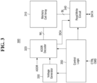
- FIG. 3 is a block diagram illustrating a nonvolatile memory of FIG. 1 .
- the electronic device 1 may include the host 100 and a memory storage device 10.
- the host 100 and the memory storage device 10 may be electrically connected.
- the host 100 may provide a logical block address LBA and a request signal REQ to the memory storage device 10, and exchange data DATA with the memory storage device 10.
- the host 100 may be connected to the memory controller 200.
- the host 100 may include, for example, a personal computer (PC), a laptop, a mobile phone, a smart phone, a tablet PC, or the like.
- PC personal computer
- laptop a mobile phone
- smart phone a tablet PC
- the memory storage device 10 may include the memory controller 200 and the nonvolatile memory 300.
- the memory storage device 10 may be integrated into one semiconductor device.
- the memory storage device 10 may include an embedded universal flash storage (UFS) memory device, an embedded multi-media card (eMMC), a solid state drive (SSD), or the like.
- the memory storage device 10 may include a removable UFS memory card, a compact flash (CF) card, a secure digital (SD) card, a micro-SD card, a mini-SD card, an extreme digital (xD) card, a memory stick, or the like.
- the nonvolatile memory 300 may include a NAND flash memory. However, embodiments of the present disclosure are not limited thereto, and the nonvolatile memory 300 may include a NOR flash memory, or a phase-change RAM (PRAM), a magneto resistive RAM (MRAM), a resistive memory such as a ferroelectric RAM (FeRAM) and a resistive RAM (RRAM).
- PRAM phase-change RAM
- MRAM magneto resistive RAM
- RRAM resistive RAM
- the memory controller 200 may be connected to the nonvolatile memory 300 to control the nonvolatile memory 300. For example, in response to the logical block address LBA, the request signal REQ, and the like received from the host 100, the memory controller 200 may provide an address ADDR, a command CMD, a control signal CTRL, and the like to the nonvolatile memory 300. The memory controller 200 may provide signals to the nonvolatile memory 300 to control writing or reading of data to or from the nonvolatile memory 300. In addition, the memory controller 200 and the nonvolatile memory 300 may exchange data DATA.
- the memory controller 200 may include a processor 210, a memory 211, a host interface 212, a memory interface 213, and a working memory 220.
- the processor 210 may include a central processing unit (CPU), a controller, an application specific integrated circuit (ASIC), or the like.
- the processor 210 may control the overall operation of the memory controller 200.
- the processor 210 may control the memory controller 200 by driving firmware loaded in the working memory 220.
- the memory 211 may store code data required for initial booting of the memory storage device 10.
- the memory controller 200 and the host 100 may be connected through the host interface 212.
- the data DATA may be transmitted and received through the host interface 212.
- the host interface 212 may include an advanced technology attachment (ATA), a serial ATA (SATA), an external SATA (e-SATA), a universal serial bus (USB), or the like.
- the memory controller 200 and the nonvolatile memory 300 may be connected through the memory interface 213.
- the data DATA, the control signal CTRL, the address ADDR, the command CMD, and the like may be transmitted and received through the memory interface 213.
- the working memory 220 may be implemented as a cache memory, a DRAM, a SRAM, a flash memory, or the like.
- the working memory 220 may include a flash translation layer (FTL).
- FTL flash translation layer
- the FTL may include system software that manages write, read, and erase operations and the like of the nonvolatile memory 300. For example, the process of converting the logical address into the physical address may be performed in the FTL.
- the FTL may include firmware.
- the FTL may be loaded into the working memory 220.
- the firmware of the FTL may be executed by the processor 210.
- the working memory 220 may include a garbage collection trigger module 222, a garbage collection manager module 224, a memory information collection module 226, and an address mapping table 228.
- a “module” may be implemented as a hardware circuit comprising custom VLSI circuits or gate arrays, off-the-shelf semiconductors such as logic chips, transistors, or other discrete components.
- a module may also be implemented in programmable hardware devices such as field programmable gate arrays, programmable array logic, programmable logic devices or the like. Modules may also be implemented in software for execution by various types of processors.
- the working memory 220 may convert the logical block address LBA into the address ADDR using the address mapping table 228 and provide it to the nonvolatile memory 300.
- the working memory 220 may perform management on memory cells of the nonvolatile memory 300.
- the working memory 220 may perform garbage collection and bad block management operations on blocks of a memory cell array 310 of the nonvolatile memory 300.
- a block may correspond to the minimum unit of erase (e.g., a region of memory whose memory cells may be erased together in the same erase operation, where portions of such region are not erased separately).
- the memory controller 200 may control garbage collection of the nonvolatile memory 300 using the garbage collection trigger module 222, the garbage collection manager module 224, and the like.
- the garbage collection trigger module 222 may provide a garbage collection trigger signal to the garbage collection manager module 224 in response to a garbage collection request.
- the garbage collection manager module 224 may control the garbage collection of the nonvolatile memory 300 using metadata or the like.
- Free blocks are blocks of the nonvolatile memory 300 that have no device valid data.
- a free block count represents the quantitative value of free blocks (e.g., the number of free blocks) of the nonvolatile memory 300.
- Garbage collection is a process for securing a free block in the nonvolatile memory 300. Since the unit of writing data is a page, and the unit of erasing data is a block, a method for adjusting the same is required. Therefore, through the garbage collection, a valid page is written to another block and a block including the valid page is erased, thereby securing a free block. The garbage collection may improve the performance of the memory storage device 10.
- the nonvolatile memory 300 may include a memory cell array 310, an address decoder 320, a voltage generator 330, a read/write circuit 340, a control logic 350, and the like.
- the memory cell array 310 may be connected to the address decoder 320 through word lines WL.
- the memory cell array 310 may be connected to the read/write circuit 340 through bit lines BL.
- the memory cell array 310 may include a plurality of memory cells. For example, the memory cells arranged in a row direction may be connected to the word line WL. For example, the memory cells arranged in a column direction may be connected to the bit line BL.
- the address decoder 320 may be connected to the memory cell array 310 through the word lines WL.
- the address decoder 320 may operate under the control of the control logic 350.
- the address decoder 320 may receive the address ADDR from the memory controller 200.
- the address decoder 320 may receive from the voltage generator 330 a voltage required for an operation such as program or read.
- the address decoder 320 may decode a row address among the received addresses ADDR.
- the address decoder 320 may select the word line WL using the decoded row address.
- a decoded column address DCA may be provided to the read/write circuit 340.
- the address decoder 320 may include a row decoder, a column decoder, an address buffer, and the like.
- the voltage generator 330 may generate a voltage required for an access operation under the control of the control logic 350.
- the voltage generator 330 may generate a program voltage and a program verification voltage which are required to perform a program operation.
- the voltage generator 330 may generate read voltages required to perform a read operation, and generate an erase voltage and an erase verification voltage required to perform an erase operation.
- the voltage generator 330 may provide a voltage required to perform each operation to the address decoder 320.
- the read/write circuit 340 may be connected to the memory cell array 310 through the bit lines BL.
- the read/write circuit 340 may exchange the data DATA with the memory controller 200.
- the read/write circuit 340 may operate under the control of the control logic 350.
- the read/write circuit 340 may receive the decoded column address DCA from the address decoder 320.
- the read/write circuit 340 may select the bit line BL using the decoded column address DCA.
- the read/write circuit 340 may program the received data DATA into the memory cell array 310.
- the read/write circuit 340 may read data from the memory cell array 310 and provide the read data to the outside (e.g., the memory controller 200).
- the read/write circuit 340 may include components such as a sense amplifier, a write driver, a column select circuit, a page buffer, and the like.
- the control logic 350 may be connected to the address decoder 320, the voltage generator 330, and the read/write circuit 340.
- the control logic 350 may control the operation of the nonvolatile memory 300.
- the control logic 350 may operate in response to the control signal CRTL and the command CMD (e.g., write command and read command) provided from the memory controller 200.
- the control logic 350 may perform the garbage collection for the memory cell array 310 under the control of the memory controller 200.
- FIG. 4 is an block diagram illustrating a nonvolatile memory device according to some embodiments.
- the nonvolatile memory 300 may include a plurality of semiconductor layers LA1 to LAn.
- Each of the plurality of semiconductor layers LA1 to LAn may be a memory chip (e.g., DRAM memory chip).
- some of the plurality of semiconductor layers LA1 to LAn may be master chips that perform interfacing with an external device (e.g., the host 100 of FIG. 1 ), and the rest of them may be slave chips that store data.
- an n th layer LAn and a first layer LA1 of the nonvolatile memory 300 may be semiconductor chips including the memory cell array 310.
- the plurality of semiconductor layers LA1 to LAn may transmit and receive signals to and from each other through a through silicon via Tab Separated Values (TSV).
- TSV Tab Separated Values
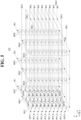
- FIG. 5 is an circuit diagram illustrating a memory cell array according to some embodiments.
- a plurality of cell strings NS11, NS21, NS31, NS12, NS22, NS32, NS13, NS23, and NS33 may be arranged in a first direction x and a second direction y on a substrate (not shown).
- the plurality of cell strings NS11, NS21, NS31, NS12, NS22, NS32, NS13, NS23, and NS33 may have a shape extending in a third direction z.
- the plurality of cell strings NS11, NS21, NS31, NS12, NS22, NS32, NS13, NS23, and NS33 may be connected in common to a common source line CSL formed on or in the substrate (not shown).
- the common source line CSL is shown as being connected to the lowermost end of the plurality of cell strings NS11, NS21, NS31, NS12, NS22, NS32, NS13, NS23, and NS33 in the third direction z.
- the common source line CSL is electrically connected to the lowermost end of the plurality of cell strings NS11, NS21, NS31, NS12, NS22, NS32, NS13, NS23, and NS33 in the third direction z, and the common source line CSL is not limited to being physically located at the lower end of the plurality of cell strings NS11, NS21, NS31, NS12, NS22, NS32, NS13, NS23, and NS33.
- the plurality of cell strings NS11, NS21, NS31, NS12, NS22, NS32, NS13, NS23, and NS33 are shown to be arranged in a 3 x 3 array in this drawing, but the arrangement shape and the number of the plurality of cell strings arranged in the memory cell array 310 of the nonvolatile memory are not limited thereto.
- Cell strings NS11, NS12, and NS13 may be connected to a first ground select line GSL1.
- Cell strings NS21, NS22, and NS23 may be connected to a second ground select line GSL2.
- Cell strings NS31, NS32, and NS33 may be connected to a third ground select line GSL3.
- cell strings NS11, NS12, and NS13 may be connected to a first string select line SSL1.
- Cell strings NS21, NS22, and NS23 may be connected to a second string select line SSL2.
- Cell strings NS31, NS32, and NS33 may be connected to a third string select line SSL3.
- Each of the plurality of cell strings NS11, NS21, NS31, NS12, NS22, NS32, NS13, NS23, and NS33 may include a string select transistor SST connected to each of the string select lines.
- each of the plurality of cell strings NS11, NS21, NS31, NS 12, NS22, NS32, NS13, NS23, and NS33 may include a ground select transistor GST connected to each of the ground select lines.
- each of the plurality of cell strings NS 11, NS21, NS31, NS12, NS22, NS32, NS13, NS23, and NS33 may be connected to the common source line CSL.
- each of the plurality of cell strings NS11, NS21, NS31, NS12, NS22, NS32, NS13, NS23, and NS33 may have a plurality of memory cells sequentially stacked in the third direction z between the ground select transistor and the string select transistor.
- each of the plurality of cell strings NS11, NS21, NS31, NS12, NS22, NS32, NS13, NS23, and NS33 may include dummy cells between the ground select transistor and the string select transistor.
- the number of the string select transistors included in each string is not limited to this drawing.
- the cell string NS11 may include a ground select transistor GST11 disposed at the lowermost end in the third direction z, a plurality of memory cells M11_1 to M11_8 sequentially stacked on the ground select transistor GST11 in the third direction z, and a string select transistor SST11 stacked on the uppermost memory cell M11_8 in the third direction z.
- the cell string NS21 may include a ground select transistor GST21 disposed at the lowermost end in the third direction z, a plurality of memory cells M21_1 to M21_8 sequentially stacked on the ground select transistor GST21 in the third direction z, and a string select transistor SST21 stacked on the uppermost memory cell M21_8 in the third direction z.
- the cell string NS31 may include a ground select transistor GST31 disposed at the lowermost end in the third direction z, a plurality of memory cells M31_1 to M31_8 sequentially stacked on the ground select transistor GST31 in the third direction z, and a string select transistor SST31 stacked on the uppermost memory cell M31_8 in the third direction z.
- the configuration of the other strings may also be similar thereto.
- the memory cells positioned at the same height in the third direction z from the substrate (not shown) or the ground select transistor may be electrically connected in common through each word line.
- the memory cells formed at the same height as the memory cells M11_1, M21_1, and M31_1 may be connected to a first word line WL1.
- the memory cells formed at the same height as the memory cells M11_2, M21_2, and M31_2 may be connected to a second word line WL2.
- a description thereof will be omitted.
- each string select transistor of the plurality of cell strings NS11, NS21, NS31, NS12, NS22, NS32, NS13, NS23, and NS33 may be connected to a bit line BL1, BL2, or BL3.
- the string select transistors SST11, SST21, and SST31 may be connected to the bit line BL1 extending in the second direction y.
- a description of the other string select transistors connected to the bit lines BL2 or BL3 is also similar to the above, and thus a description thereof will be omitted.
- the memory cells corresponding to one string (or ground) select line and one word line may form one page.
- a write operation and a read operation may be performed on a page basis.
- Each of the memory cells in each page may store two or more bits. Bits written to the memory cells of each page may form logical pages.
- the memory cell array 310 may be provided as a three-dimensional memory array.
- the three-dimensional memory array may be monolithically formed on one or more physical levels of arrays of the memory cells having an active area disposed on a substrate (not shown) and a circuit involved in the operation of the memory cells.
- the circuit involved in the operation of the memory cells may be located within or on the substrate. Being monolithically formed means that layers of each level of the three-dimensional array may be deposited directly on the lower level layers of the three-dimensional array. Alternatively, the circuit involved in the operation of the memory cells may be connected to a contact portion of the uppermost end in the third direction z. This will be described in detail with reference to FIG. 6 .
- FIG. 6 is an diagram schematically illustrating an inside of a nonvolatile memory according to some embodiments.
- the nonvolatile memory 300 may have a chip to chip (C2C) structure.
- a cell region CELL of the nonvolatile memory 300 may correspond to the memory cell array 310 of FIG. 5 .
- the C2C structure may include a structure obtained by manufacturing an upper chip including a cell region CELL on a first wafer, manufacturing a lower chip including a peripheral circuit region PERI on a second wafer different from the first wafer, and connecting the upper chip and the lower chip to each other by a bonding method.
- the bonding method may include a method of electrically connecting a bonding metal formed on an uppermost metal layer of the upper chip to a bonding metal formed on an uppermost metal layer of the lower chip.
- the bonding metal is formed of copper (Cu)
- the bonding method may be a Cu-Cu bonding method, and the bonding metal may also be formed of aluminum or tungsten.
- the peripheral circuit region PERI and the cell region CELL of the nonvolatile memory 300 may each include an external pad bonding area PA, a word line bonding area WLBA, and a bit line bonding area BLBA.
- the peripheral circuit region PERI may include a first substrate 1210, an interlayer insulating layer 1215, a plurality of circuit elements 1220a, 1220b, and 1220c formed on the first substrate 1210, a first metal layer 1230a, 1230b, and 1230c connected to each of the plurality of circuit elements 1220a, 1220b, and 1220c, and a second metal layer 1240a, 1240b, and 1240c formed on the first metal layer 1230a, 1230b, and 1230c.
- the first metal layer 1230a, 1230b, and 1230c may be formed of tungsten having a relatively high resistance
- the second metal layer 1240a, 1240b, and 1240c may be formed of copper having a relatively low resistance.
- first metal layer 1230a, 1230b, and 1230c and the second metal layer 1240a, 1240b, and 1240c are illustrated and described, but the present disclosure is not limited thereto, and one or more metal layers may be further formed on the second metal layer 1240a, 1240b, and 1240c. At least some of the one or more metal layers formed on the second metal layer 1240a, 1240b, and 1240c may be formed of aluminum or the like having a lower resistance than copper forming the second metal layer 1240a, 1240b, and 1240c.
- the interlayer insulating layer 1215 may be disposed on the first substrate 1210 to cover the plurality of circuit elements 1220a, 1220b, and 1220c, the first metal layer 1230a, 1230b, and 1230c, and the second metal layer 1240a, 1240b, and 1240c, and may include an insulating material such as silicon oxide or silicon nitride.
- Lower bonding metals 1271b and 1272b may be formed on the second metal layer 1240b in the word line bonding area WLBA.
- the lower bonding metals 1271b and 1272b of the peripheral circuit region PERI may be electrically connected to upper bonding metals 1371b and 1372b of the cell region CELL by a bonding method.
- the lower bonding metals 1271b and 1272b and the upper bonding metals 1371b and 1372b may be formed of aluminum, copper, tungsten, or the like.
- the cell region CELL may provide at least one memory block.
- the cell region CELL may include a second substrate 1310 and a common source line 1320 (corresponding to CSL of FIG. 5 ).
- a plurality of word lines 1330 (1331 to 1338, corresponding to WL1 to WL8 of FIG. 5 ) may be stacked along the third direction z perpendicular to the top surface of the second substrate 1310.
- String select lines and a ground select line may be disposed above and below the word lines 1330, respectively, and the plurality of word lines 1330 may be disposed between the string select lines and the ground select line.
- a channel structure CH may extend in a direction perpendicular to the top surface of the second substrate 1310 to penetrate the word lines 1330, the string select lines, and the ground select line.
- the channel structure CH may include a data storage layer, a channel layer, a buried insulating layer, and the like.
- the channel layer may be electrically connected to a first metal layer 1350c and a second metal layer 1360c.
- the first metal layer 1350c may be a bit line contact
- the second metal layer 1360c may be a bit line (corresponding to BL1 to BL3 of FIG. 5 ).
- the bit line 1360c may extend along the second direction y parallel to the top surface of the second substrate 1310.
- an area in which the channel structure CH and the bit line 1360c are disposed may be defined as the bit line bonding area BLBA.
- the bit line 1360c may be electrically connected to the circuit elements 1220c that provide a page buffer 1393 in the peripheral circuit region PERI.
- the bit line 1360c may be connected to an upper bonding metal 1371c and 1372c in the peripheral circuit region PERI, and the upper bonding metal 1371c and 1372c may be connected to a lower bonding metal 1271c and 1272c connected to the circuit elements 1220c of the page buffer 1393.
- the word lines 1330 may extend along the first direction x parallel to the top surface of the second substrate 1310, and may be connected to a plurality of cell contact plugs 1340 (1341 to 1347).
- the word lines 1330 and the cell contact plugs 1340 may be connected to each other in pads provided by at least some of the word lines 1330 extending with different lengths along the first direction x.
- a first metal layer 1350b and a second metal layer 1360b may be sequentially connected to the top portions of the cell contact plugs 1340 connected to the word lines 1330.
- the cell contact plugs 1340 may be connected to the peripheral circuit region PERI through the upper bonding metals 1371b and 1372b of the cell region CELL and the lower bonding metals 1271b and 1272b of the peripheral circuit region PERI.
- the cell contact plugs 1340 may be electrically connected to the circuit elements 1220b that provide a row decoder 1394 in the peripheral circuit region PERI.
- the operating voltage of the circuit elements 1220b providing the row decoder 1394 may be different from the operating voltage of the circuit elements 1220c providing the page buffer 1393.
- the operating voltage of the circuit elements 1220c providing the page buffer 1393 may be greater than the operating voltage of the circuit elements 1220b providing the row decoder 1394.
- a common source line contact plug 1380 may be disposed in the external pad bonding area PA.
- the common source line contact plug 1380 may be formed of a conductive material such as a metal, a metal compound, or polysilicon, and may be electrically connected to the common source line 1320.
- a first metal layer 1350a and a second metal layer 1360a may be sequentially stacked on the common source line contact plug 1380.
- an area in which the common source line contact plug 1380, the first metal layer 1350a, and the second metal layer 1360a are disposed may be defined as the external pad bonding area PA.
- input/output pads 1205 and 1305 may be disposed in the external pad bonding area PA.
- a lower insulating layer 1201 may be formed to cover the bottom surface of the first substrate 1210, and a first input/output pad 1205 may be formed on the lower insulating layer 1201.
- the first input/output pad 1205 may be connected to at least one of the plurality of circuit elements 1220a, 1220b, and 1220c disposed in the peripheral circuit region PERI through a first input/output contact plug 1203, and may be separated from the first substrate 1210 by the lower insulating layer 1201.
- a side insulating layer may be disposed between the first input/output contact plug 1203 and the first substrate 1210 to electrically separate the first input/output contact plug 1203 from the first substrate 1210.
- an upper insulating layer 1301 may be formed on the second substrate 1310 to cover the top surface of the second substrate 1310, and a second input/output pad 1305 may be disposed on the upper insulating layer 1301.
- the second input/output pad 1305 may be connected to at least one of the plurality of circuit elements 1220a, 1220b, and 1220c disposed in the peripheral circuit region PERI through a second input/output contact plug 1303.
- the second substrate 1310, the common source line 1320, and the like may not be disposed in an area where the second input/output contact plug 1303 is disposed.
- the second input/output pad 1305 may not overlap the word lines 1330 in the third direction z.
- the second input/output contact plug 1303 may be separated from the second substrate 1310 in a direction parallel to the top surface of the second substrate 1310, and may penetrate an interlayer insulating layer 1315 of the cell region CELL to be connected to the second input/output pad 1305.
- the first input/output pad 1205 and the second input/output pad 1305 may be selectively formed.
- the nonvolatile memory 300 may include only the first input/output pad 1205 disposed below the first substrate 1210, or only the second input/output pad 1305 disposed above the second substrate 1310.
- the nonvolatile memory 300 may include both the first input/output pad 1205 and the second input/output pad 1305.
- an uppermost metal layer may have a metal pattern existing as a dummy pattern, or may be empty.
- a lower metal pattern 1273a having the same shape as the upper metal pattern 1372a of the cell region CELL may be formed in an uppermost metal layer of the peripheral circuit region PERI.
- the lower metal pattern 1273a formed on the uppermost metal layer of the peripheral circuit region PERI may not be connected to a separate contact in the peripheral circuit region PERI.
- the upper metal pattern 1372a may be electrically connected to upper bonding metal 1371a by a bonding method.
- the upper bonding metal 1371a may be electrically connected to second metal layer 1360a.
- the upper metal pattern 1373a having the same shape as the lower metal pattern 1273a of the peripheral circuit region PERI may be formed in the upper metal layer of the cell region CELL.
- the upper metal pattern 1373a may be electrically connected to second input/output contact plug 1303.
- Lower bonding metal 1271a may be electrically connected to the lower metal pattern 1272a by a bonding method.
- the lower bonding metal 1271a may be electrically connected to the first metal layer in the external pad bonding area PA.
- the lower bonding metals 1271b and 1272b may be formed on the second metal layer 1240b in the word line bonding area WLBA.
- the lower bonding metals 1271b and 1272b of the peripheral circuit region PERI may be electrically connected to the upper bonding metals 1371b and 1372b of the cell region CELL by a bonding method.
- an upper metal pattern 1392 having the same shape as the lower metal pattern 1252 of the peripheral circuit region PERI may be formed in the uppermost metal layer of the cell region CELL.
- a contact may not be formed on the upper metal pattern 1392 formed in the uppermost metal layer of the cell region CELL.
- the electronic device 1 including a garbage collection prediction module 130 will be described with reference to FIGS. 7 and 8 .
- FIG. 7 is a block diagram illustrating an electronic device according to some embodiments.
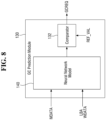
- FIG. 8 is a block diagram illustrating a garbage collection prediction module of FIG. 7 .
- the host 100 may include an application processor 110, a memory 120, and the garbage collection prediction module 130.
- an application processor 110 may include an application processor 110, a memory 120, and the garbage collection prediction module 130.
- embodiments according to the present disclosure are not limited thereto, and some configurations may be omitted.
- the application processor 110 may control the overall operation of the host 100. For example, the application processor 110 may receive the logical block address LBA and write data WDATA stored in the memory 120. The application processor 110 may transmit the logical block address LBA and the write data WDATA to the memory controller 200 together with a write request signal WREQ. This operation may be calculated and performed by the application processor 110.
- the memory 120 may store data to be used in the application processor 110 and the garbage collection prediction module 130.
- the memory 120 may receive data to temporarily store it, and transmit the data to the application processor 110 and the garbage collection prediction module 130 when the data is required.
- the memory 120 may receive and store data from the application processor 110 and the garbage collection prediction module 130.
- the garbage collection prediction module 130 may receive the logical block address LBA and the write data WDATA from the memory 120 or the application processor 110. In addition, the garbage collection prediction module 130 may receive metadata MDATA from the memory controller 200.
- the garbage collection prediction module 130 may train a neural network model 140 using at least one of the received logical block address LBA, write data WDATA, and metadata MDATA.
- the garbage collection prediction module 130 may provide a garbage collection request signal GCREQ, the logical block address LBA, and the like to the memory controller 200 based on the trained neural network model 140. A more detailed description of the garbage collection prediction module 130 will be described later.
- the memory controller 200 may include a data write module 230, the garbage collection trigger module 222, the garbage collection manager module 224, and the memory information collection module 226.
- the data write module 230 may include the address mapping table 228.
- the data write module 230 may receive the logical block address LBA, the write data WDATA, and the write request signal WREQ from the application processor 110. In response to the write request signal WREQ, the data write module 230 may control the nonvolatile memory 300 to write the write data WDATA to the nonvolatile memory 300.
- the data write module 230 may convert the logical block address LBA into the address ADDR based on the address mapping table 228.
- the address ADDR may be a physical block address.
- the address mapping table 228 may be changed under the control of the memory controller 200.
- the data write module 230 may provide the address ADDR, a write command WCMD, and the write data WDATA to the nonvolatile memory 300.
- the nonvolatile memory 300 may write the write data WDATA to a block of the memory cell array 310 corresponding to the address ADDR.
- embodiments according to the present disclosure are not limited thereto, and the nonvolatile memory 300 may perform a read operation or an erase operation.
- the garbage collection trigger module 222 may receive the garbage collection request signal GCREQ from the host 100 and control the memory controller 200 so that the garbage collection is performed. For example, the garbage collection trigger module 222 may receive the garbage collection request signal GCREQ and the logical block address LBA from the garbage collection prediction module 130.
- the garbage collection trigger module 222 may provide a garbage collection trigger signal GCTS and the logical block address LBA to the garbage collection manager module 224.
- the garbage collection may be performed by the operation of the garbage collection trigger module 222. If the garbage collection trigger module 222 does not transmit the garbage collection trigger signal GCTS to the garbage collection manager module 224, the garbage collection of the memory storage device 10 may not be performed.
- the garbage collection manager module 224 may receive the garbage collection trigger signal GCTS from the garbage collection trigger module 222 and in response thereto, may control the nonvolatile memory 300 to perform the garbage collection.
- the garbage collection manager module 224 may transmit the address ADDR corresponding to the logical block address LBA to the nonvolatile memory 300 and transmit a garbage collection signal GCS.
- the garbage collection signal GCS may include a write command and an erase command, but embodiments according to the present disclosure are not limited thereto.
- the nonvolatile memory 300 may perform the garbage collection by the garbage collection manager module 224. For example, a valid page of a block corresponding to the address ADDR may be copied to another block. In addition, the block corresponding to the address ADDR may be erased. The block corresponding to the address ADDR may become a free block, and accordingly, the performance of the memory storage device 10 may be improved.
- the garbage collection manager module 224 may receive the metadata MDATA from the memory information collection module 226.
- the garbage collection manager module 224 may allow the garbage collection to be performed with a small garbage collection cost using the provided metadata MDATA.
- the memory information collection module 226 may receive and collect the metadata MDATA from the nonvolatile memory 300.
- the metadata MDATA may include FTL metadata.
- the metadata MDATA may indicate the number of free blocks in the nonvolatile memory 300, writable page information of an update block, the number of valid pages, the number of erases of all blocks, the number of valid pages of blocks that manage page mapping, and the like.
- the metadata MDATA may further include information on the nonvolatile memory 300 after a write operation is performed.
- the metadata MDATA may include information on the nonvolatile memory 300 after the write operation is performed in the nonvolatile memory 300 by the write command WCMD. For example, assuming that the number of free blocks included in the nonvolatile memory 300 before the write operation is performed is 100 and the number of free blocks included in the nonvolatile memory 300 after the write operation is performed is 50, the metadata MDATA may include data recording that the number of free blocks has been changed from 100 to 50.
- the memory information collection module 226 may provide the metadata MDATA to the garbage collection manager module 224 and the host 100.
- the metadata MDATA may be processed by the memory controller 200 and then provided to the host 100.
- the memory information collection module 226 may provide the metadata MDATA to the garbage collection prediction module 130. Then, the garbage collection prediction module 130 may receive the metadata MDATA that is data for the nonvolatile memory 300 and train the neural network model 140 to predict when the garbage collection should be performed.
- the garbage collection prediction module 130 may include the neural network model 140 and a comparator 132.
- embodiments according to the present disclosure are not limited thereto, and may include other configurations.
- the neural network model 140 may receive the metadata MDATA, the logical block address LBA, the write data WDATA, and the like.
- the neural network model 140 may be trained based on the received metadata MDATA, logical block address LBA, write data WDATA, and the like.
- the training method of the neural network model 140 may include deep learning, machine learning, or the like.
- the garbage collection prediction module 130 may output a garbage collection prediction value using the trained neural network model 140.
- the comparator 132 may receive the garbage collection prediction value and compare it with a reference value REF_VAL.
- the comparator 132 may output the garbage collection request signal GCREQ based on the comparison result. For example, when the comparison result does not satisfy a criterion, the comparator 132 may not output the garbage collection request signal GCREQ.
- FIG. 9 is a flowchart illustrating a garbage collection prediction operation of an electronic device according to some embodiments.
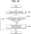
- FIG. 10 is a flowchart illustrating the garbage collection prediction operation of FIG. 9 in more detail.
- the memory storage device 10 may perform a write operation (step S400).
- the address ADDR, the write command WCMD, and the write data WDATA may be transmitted from the memory controller 200 to the nonvolatile memory 300, and the write data WDATA may be written to the nonvolatile memory 300.
- the write operation of the memory storage device 10 may be performed multiple times instead of once.
- the write operation of the memory storage device 10 is not limited to one time and may be performed multiple times for the same address ADDR.
- the memory 120 of the host 100 may store host data (step S401). For example, the memory 120 of the host 100 may receive and store the logical block address LBA, the write data WDATA, and the like from the application processor 110. Further, the memory 120 may provide the stored logical block address LBA, write data WDATA, and the like to the garbage collection prediction module 130. For example, the garbage collection prediction module 130 may receive the logical block address LBA, write data WDATA, and the like that have been used in the write operation.
- the memory information collection module 226 of the memory controller 200 may receive the metadata MDATA from the nonvolatile memory 300 (step S402).
- the garbage collection prediction module 130 of the host 100 will receive and store the metadata MDATA from the memory information collection module 226 (step S403).
- the garbage collection prediction module 130 will perform a garbage collection prediction using the neural network model 140 trained with the stored data (step S404).
- the garbage collection prediction module 130 will train the neural network model 140 using the received logical block address LBA, write data WDATA, metadata MDATA, and the like.
- the garbage collection prediction module 130 may train the neural network model 140 using the metadata MDATA for the nonvolatile memory 300 after each of a plurality of write operations is performed.
- the garbage collection prediction module 130 will determine whether the garbage collection is predicted using the trained neural network model 140 (step S405). If the garbage collection is not predicted (NO in step S405), the steps S400 to S405 may be repeated. If the garbage collection is predicted (YES in step S405), the garbage collection may be performed (step S406). For example, the garbage collection prediction module 130 will transmit the garbage collection request signal GCREQ to the garbage collection trigger module 222, so that the garbage collection is performed.
- FIG. 10 for a more detailed garbage collection prediction operation of the garbage collection prediction module 130.
- FIG. 10 it is assumed that only a free block count FBC of the information included in the metadata MDATA is used.
- FBC free block count
- the garbage collection prediction module 130 may predict the free block count of the nonvolatile memory 300 (step S407). For example, the garbage collection prediction module 130 may predict, at a current time period t n , the free block count of the nonvolatile memory at a future time period t n+1 in which a write operation is performed/executed with respect to the nonvolatile memory 300. The current time period t n occurs subsequent to a past time period t n-1 in which one or more write operations have been performed/executed with respect to the nonvolatile memory 300. Specifically, the garbage collection prediction module 130 may train the neural network model using the free block count resulting from previous write operations, and predict the free block count after a subsequent write operation using the trained neural network model. For example, the garbage collection prediction module 130 may output the predicted free block count.
- the garbage collection prediction module 130 may determine whether the predicted free block count is smaller than the reference value REF_VAL (step S408).
- the garbage collection prediction operation may be terminated.
- the garbage collection prediction module 130 may not provide the garbage collection request signal GCREQ to the memory controller 200.
- the garbage collection prediction module 130 may provide the garbage collection request signal GCREQ to the memory controller 200. Accordingly, the memory storage device 10 may perform the garbage collection. For example, even if a garbage collection condition is not yet satisfied, when a predicted garbage collection condition is satisfied, the garbage collection of the memory storage device 10 may be performed. Accordingly, a load caused by the garbage collection of the memory storage device 10 may be reduced, and the performance of the memory storage device 10 may be improved.
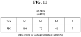
- FIGS. 11 to 14 are diagrams illustrating a garbage collection prediction operation using a neural network, according to some embodiments.
- the garbage collection prediction module 130 uses the free block count FBC of the nonvolatile memory 300 among the metadata MDATA.
- the free block count FBC of the nonvolatile memory 300 may change over time. For example, after the write operation is performed at time t-3, the free block count FBC of the nonvolatile memory 300 may be 100. For example, after the write operation is performed at time t-2, the free block count FBC of the nonvolatile memory 300 may be 70. For example, after the write operation is performed at time t-1, the free block count FBC of the nonvolatile memory 300 may be 40.
- the free block count FBC of the nonvolatile memory 300 in each time period may be, or may be included in, metadata MDATA provided from the nonvolatile memory 300.
- a criterion of the free block count FBC for performing the garbage collection may be smaller than 20. For example, when the free block count FBC of the nonvolatile memory 300 is 20 or more, the garbage collection is not performed, and when the free block count FBC of the nonvolatile memory 300 is smaller than 20, the garbage collection may be performed.
- the neural network model 140 may include an input layer 141, hidden layers 142 and 143, and an output layer 144.
- the neural network model 140 may perform computation based on received input data I1 and I2 and generate output data O1 and O2 based on the computation result.
- the neural network model 140 may be trained by performing computation based on the input data I1 and I2.
- the input data I1 and I2 used for training the neural network model 140 may be training data.
- the neural network model 140 may be a deep neural network including two or more hidden layers.
- the neural network model 140 may include convolutional neural networks (CNN), recurrent neural networks (RNN), deep belief networks, restricted boltzman machines, or the like.
- Each of the layers 141, 142, 143, and 144 included in the neural network model 140 may include a plurality of neurons.
- the neurons may correspond to multiple artificial nodes.
- the input layer 141 may include two neurons, and each of the hidden layers 142 and 143 may include three neurons.
- embodiments according to the present disclosure are not limited thereto, and each of the layers included in the neural network model 140 may include various numbers of neurons.
- the neurons included in the neural network model 140 may be connected to each other and exchange data.
- One neuron may receive and compute data from other neurons, and output the computation result to still other neurons.
- each neuron may be input activation and output activation.
- the activation may be a parameter that corresponds to not only the output of one neuron but also the input of neurons included in the next layer.
- each neuron may determine its own activation based on activations and weights received from neurons included in the previous layer.
- the weight is a parameter used to calculate the output activation in each neuron, and may be a value assigned to a connection relationship between neurons.
- the neural network model 140 In the neural network model 140, numerous data sets are exchanged between a plurality of interconnected neurons, and undergo numerous computational processes while passing through layers. Meanwhile, the neural network model 140 is trained through such computational processes, and weights and biases may be optimized based thereon.
- the free block count FBC of the nonvolatile memory 300 in each time period may be an input of the neural network model 140.
- the free block count FBC of the nonvolatile memory 300 at times t-3, t-2, and t-1 may be inputted to the neural network model 140.
- the neural network model 140 may be trained using the corresponding inputs, and accordingly, the garbage collection prediction module 130 may output a result that the free block count FBC of the nonvolatile memory 300 is predicted to be 10.
- the free block count FBC of the nonvolatile memory 300 was 100 at time t-3, 70 at time t-2, and 40 at time t-1.
- the neural network model 140 is trained using such data, and as a result, the garbage collection prediction module 130 may output a result that the free block count FBC of the nonvolatile memory 300 is 10 at time t.
- a predicted value of the free block count FBC of the nonvolatile memory 300 when the next write operation is performed may be 10. Accordingly, the garbage collection prediction module 130 may compare the reference value REF_VAL of 20 with the predicted value of 10 through the comparator 132. Since the predicted value is smaller than the reference value REF_VAL, the garbage collection prediction module 130 may provide the garbage collection request signal GCREQ to the memory controller 200 so that the garbage collection is performed.
- the garbage collection may be performed at a time period when the garbage collection performance criterion is not satisfied. For example, by predicting a time period when the garbage collection is performed, a load caused by the garbage collection may be reduced, and the performance of the memory storage device 10 may be further improved.
- FIG. 15 is a ladder diagram illustrating a garbage collection operation in an electronic device according to some embodiments.
- the host 100 may provide the logical block address LBA, the write request signal WREQ, and first write data WDATA1 to the memory controller 200 (step S410).
- the memory controller 200 may execute a program in response to the write request signal WREQ (step S411).
- the memory controller 200 may provide the address ADDR, the write command WCMD, and the first write data WDATA1 to the nonvolatile memory 300 (step S412).
- the nonvolatile memory 300 may write the first write data WDATA1 in response to the write command WCMD provided from the memory controller 200 (step S413).
- the nonvolatile memory 300 may provide first metadata MDATA1 to the host 100 (step S414).
- the nonvolatile memory 300 may provide the first metadata MDATA1 to the memory information collection module 226 of the memory controller 200.
- the memory information collection module 226 of the memory controller 200 may provide the received first metadata MDATA1 to the host 100.
- the host 100 may store at least one of the logical block address LBA, the first write data WDATA1, or the first metadata MDATA1 (step S415).
- the host 100 may perform garbage collection prediction using the neural network model 140 (step S416).
- the neural network model 140 may be trained using at least one of the logical block address LBA, the first write data WDATA1, or the first metadata MDATA1.
- the garbage collection prediction module 130 of the host 100 may output a predicted value using the trained neural network model 140.
- the garbage collection prediction module 130 may compare the predicted value with the reference value and, if the criterion is satisfied, provide the garbage collection request signal GCREQ and the logical block address LBA to the memory controller 200 (step S417).
- the memory controller 200 may perform the garbage collection in response to the garbage collection request signal GCREQ (step S418).
- the garbage collection manager module 224 may perform the garbage collection for the nonvolatile memory 300 by the garbage collection trigger module 222.
- the memory controller 200 may provide the address ADDR, the write command WCMD, and an erase command ECMD to the nonvolatile memory 300 (step S419).
- the nonvolatile memory 300 may copy and erase a valid page of a block corresponding to the address ADDR, thereby performing the garbage collection (step S420).
- the host 100 may provide the logical block address LBA, the write request signal WREQ, and second write data WDATA2 to the memory controller 200 (step S421).
- the certain time period corresponds to a time period after the garbage collection is performed, and does not necessarily have to be a regular time period.
- the second write data WDATA2 may be different from the first write data WDATA1.
- the memory controller 200 may execute a program in response to the received write request signal WREQ (step S422). Accordingly, the memory controller 200 may provide the address ADDR, the write command WCMD, and the second write data WDATA2 to the nonvolatile memory 300 (step S423).
- the nonvolatile memory 300 may write the second write data WDATA2 in response to the write command WCMD (step S424).
- the garbage collection is performed to generate a free block, and the second write data WDATA2 may be written to a newly generated free block. Accordingly, a load generated when the garbage collection is performed after the second write data WDATA2 is written may be reduced, and thus the overall performance of the memory storage device 10 may be improved.
- FIGS. 16 to 18 are diagrams illustrating a garbage collection prediction operation using a neural network, according to some embodiments.
- the garbage collection prediction module 130 uses the logical block address cumulative count LBA_AC.
- the logical block address cumulative count LBA_AC provided by the host 100 may change over time. For example, after the write operation is performed, the logical block address cumulative count LBA_AC may be 0 at time t-3. For example, after the write operation is performed, the logical block address cumulative count LBA_AC may be 30 at time t-2. For example, after the write operation is performed, the logical block address cumulative count LBA_AC may be 60 at time t-1.
- the logical block address cumulative count LBA_AC in each time period may be data derived from the logical block address LBA and the write data WDATA.
- a criterion of the logical block address cumulative count LBA_AC for performing the garbage collection may be greater than 80. For example, when the logical block address cumulative count LBA_AC is 80 or less, the garbage collection may not be performed, and when the logical block address cumulative count LBA_AC is greater than 80, the garbage collection may be performed.
- the logical block address cumulative count LBA_AC in each time period may be an input of the neural network model 140.
- the logical block address cumulative count LBA_AC at times t-3, t-2, and t-1 may be inputted to the neural network model 140.
- the neural network model 140 may be trained using the corresponding inputs, and accordingly, the garbage collection prediction module 130 may output a result that the logical block addresses cumulative count LBA_AC of the nonvolatile memory 300 is predicted to be 90.
- the logical block address cumulative count LBA_AC was 0 at time t-3, 30 at time t-2, and 60 at time t-1.
- the neural network model 140 is trained using such data, and as a result, the garbage collection prediction module 130 may output a result that the logical block address cumulative count LBA_AC is 90 at time t.
- a predicted value of the logical block address cumulative count LBA_AC may be 90. Accordingly, the garbage collection prediction module 130 may compare the reference value REF_VAL of 80 with the predicted value of 90 through the comparator 132. Accordingly, since the predicted value is greater than the reference value REF_VAL, the garbage collection predicting module 130 may provide the garbage collection request signal GCREQ to the memory controller 200 so that the garbage collection is performed.
- the garbage collection may be performed at a time period when the garbage collection performance criterion is not satisfied. For example, by predicting a time period when the garbage collection is performed, a load caused by the garbage collection may be reduced, and the performance of the memory storage device 10 may be further improved.
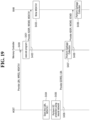
- FIG. 19 is a ladder diagram illustrating a garbage collection operation in an electronic device according to some embodiments.
- the host 100 may provide the logical block address LBA, the write request signal WREQ, and the first write data WDATA1 to the memory controller 200 (step S430).
- the memory controller 200 may execute a program in response to the write request signal WREQ (step S431).
- the memory controller 200 may provide the address ADDR, the write command WCMD, and the first write data WDATA1 to the nonvolatile memory 300 (step S432).
- the nonvolatile memory 300 may write the first write data WDATA1 in response to the write command WCMD provided from the memory controller 200 (step S433).
- the host 100 may store at least one of the logical block address LBA or the first write data WDATA1 (step S434). Then, the host 100 may perform garbage collection prediction using the neural network model 140 (step S435). For example, the neural network model 140 may be trained using at least one of the logical block address LBA or the first write data WDATA1.
- the garbage collection prediction module 130 of the host 100 may output a predicted value using the trained neural network model 140.
- the garbage collection prediction module 130 may compare the predicted value with the reference value and, if the criterion is satisfied, provide the garbage collection request signal GCREQ and the logical block address LBA to the memory controller 200 (step S436).
- the memory controller 200 may perform the garbage collection in response to the garbage collection request signal GCREQ (step S437).
- the garbage collection manager module 224 may perform the garbage collection for the nonvolatile memory 300 by the garbage collection trigger module 222.
- the memory controller 200 may provide the address ADDR, the write command WCMD, and the erase command ECMD to the nonvolatile memory 300 (step S438).
- the nonvolatile memory 300 may copy and erase a valid page of a block corresponding to the address ADDR, thereby performing the garbage collection (step S439).
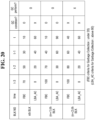
- FIGS. 20 and 21 are diagrams illustrating a garbage collection prediction operation using a neural network, according to some embodiments.
- the condition for the free block count FBC of the nonvolatile memory 300 may be satisfied, but the condition for the logical block address cumulative count LBA_AC may not be satisfied.
- both the condition for the free block count FBC of the nonvolatile memory 300 and the condition for the logical block address cumulative count LBA_AC may be satisfied.
- both the condition for the logical block address cumulative count LBA_AC and the condition for the free block count FBC of the nonvolatile memory 300 may not be satisfied.
- the garbage collection for the nonvolatile memory 300 may be performed.
- the garbage collection for the n th block and the (n+1) th block may be performed.
- the garbage collection for the (n+2) th block may not be performed since the condition is not satisfied.
- the garbage collection prediction module 130 may include the neural network model 140 and a determiner 131.
- the neural network model 140 may include a first neural network model 145 and a second neural network model 146.
- the first neural network model 145 may be trained using the free block count FBC of the nonvolatile memory 300.
- the second neural network model 146 may be trained using the logical block address cumulative count LBA_AC.
- the determiner 131 may receive a result from the first neural network model 145 and the second neural network model 146 and, if at least one condition is satisfied, transmit the garbage collection request signal GCREQ to the memory controller 200. For example, the determiner 131 may output a result according to a table of FIG. 20 .
- the neural network model 140 is described as being trained using only one of the metadata MDATA and the logical block address LBA, but embodiments according to the present disclosure are not limited thereto.
- the neural network model 140 may be trained using all of the metadata MDATA, the write data WDATA, and the logical block address LBA.
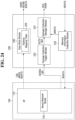
- the electronic device 1 including the memory controller 200 having a garbage collection prediction module 240 will be described with reference to FIGS. 22 and 23 .
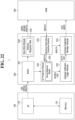
- FIG. 22 is a block diagram illustrating an electronic device according to some embodiments.
- FIG. 23 is a ladder diagram illustrating a garbage collection operation in the electronic device of FIG. 22 .
- a description overlapping with the description with reference to FIGS. 1 to 21 will be briefly given or omitted.
- the host 100 may include the application processor 110 and the memory 120.
- the memory controller 200 may include a buffer 231, the data write module 230, the garbage collection trigger module 222, the garbage collection manager module 224, the memory information collection module 226, and the garbage collection prediction module 240.
- the host 100 may not include the garbage collection prediction module 240, but the memory controller 200 may include the garbage collection prediction module 240.
- the application processor 110 may provide the logical block address LBA, the write request signal WREQ, and the write data WDATA to the buffer 231.
- the buffer 231 may temporarily store the received logical block address LBA, write request signal WREQ, and write data WDATA.
- the buffer 231 may provide the stored logical block address LBA, write request signal WREQ, and write data WDATA to the data write module 230. Further, the buffer 231 may provide the stored logical block address LBA and write data WDATA to the garbage collection prediction module 240.
- the garbage collection prediction module 240 included in the memory controller 200 may be the same as the garbage collection prediction module 130 described above.
- the garbage collection prediction module 240 may predict a time period when the garbage collection is performed using a trained neural network model 250.
- the garbage collection prediction module 240 may receive the logical block address LBA, the write data WDATA, and the metadata MDATA, and train the neural network model 250 using at least one of the logical block address LBA, the write data WDATA, or the metadata MDATA.
- the garbage collection prediction module 240 may provide the garbage collection request signal GEREQ and the logical block address LBA to the garbage collection trigger module 222. Accordingly, the memory controller 200 may perform the garbage collection for the nonvolatile memory 300.
- the host 100 may provide the logical block address LBA, the write request signal WREQ, and the first write data WDATA1 to the memory controller 200 (step S440).
- the memory controller 200 may execute a program in response to the write request signal WREQ (step S441).
- the memory controller 200 may provide the address ADDR, the write command WCMD, and the first write data WDATA1 to the nonvolatile memory 300 (step S442).
- the nonvolatile memory 300 may write the first write data WDATA1 in response to the write command WCMD provided from the memory controller 200 (step S443).
- the nonvolatile memory 300 may provide the first metadata MDATA1 to the host 100 (step S444).
- the nonvolatile memory 300 may provide the first metadata MDATA1 to the memory information collection module 226 of the memory controller 200.
- the memory information collection module 226 of the memory controller 200 may provide the received first metadata MDATA1 to the garbage collection prediction module 240 of the memory controller 200.
- the garbage collection prediction module 240 may store the logical block address LBA, the first write data WDATA1, and the first metadata MDATA1 (step S445).
- the garbage collection prediction module 240 may perform garbage collection prediction by using the neural network model 250 trained using at least one of the logical block address LBA, the first write data WDATA1, or the first metadata MDATA1 (step S446).
- the garbage collection prediction module 240 may output a predicted value using the trained neural network model 250.
- the garbage collection prediction module 240 may compare the predicted value with the reference value and, if the criterion is satisfied, provide the address ADDR, the write command WCMD, and the erase command ECMD to the nonvolatile memory 300 (step S447).
- the nonvolatile memory 300 may receive the address ADDR, the write command WCMD, and the erase command ECMD to perform the garbage collection for the memory cell array 310 (step S448).
- the memory controller 200 may include the garbage collection prediction module 240.
- the garbage collection prediction may be performed by the memory controller 200 itself.
- the electronic device 1 including the host 100 having the application processor 110 will be described with reference to FIG. 24 .
- FIG. 24 is a block diagram illustrating an electronic device according to some embodiments. For simplicity of description, a description overlapping with the description with reference to FIGS. 1 to 21 will be briefly given or omitted.
- the host 100 may include the application processor 110.
- the application processor 110 may include the neural network model 140.
- the host 100 may not include the memory 120 and the garbage collection prediction module 130.
- the application processor 110 may perform the function of the garbage collection prediction module 130 instead.
- the functions of the memory 120 and the garbage collection prediction module 130 may be implemented only by the application processor 110.
- the application processor 110 may provide the logical block address LBA, the write request signal WREQ, and the write data WDATA to the memory controller 200.
- the application processor 110 may receive the metadata MDATA from the memory controller 200 to train the neural network model 140.
- the application processor 110 may provide the garbage collection request signal GCREQ and the logical block address LBA to the memory controller 200, using the trained neural network model 140.
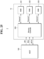
- an electronic device 2 including a plurality of nonvolatile memories 301, 302, and 303 will be described with reference to FIG. 25 .
- FIG. 25 is a block diagram illustrating an electronic device according to some embodiments. For simplicity of description, a description overlapping with the description with reference to FIGS. 1 to 24 will be briefly given or omitted.
- the memory storage device 10 may include the plurality of nonvolatile memories 301, 302, and 303 connected to the memory controller 200.
- Each of the nonvolatile memories 301, 302, and 303 may be substantially the same as the nonvolatile memory 300 described with reference to FIG. 3 .
- each of the nonvolatile memories 301, 302, and 303 may include the memory cell array 310, the address decoder 320, the voltage generator 330, the read/write circuit 340, the control logic 350, and the like.
- the memory controller 200 and the nonvolatile memory 301 may be connected through a first channel 1.
- the memory controller 200 and the nonvolatile memory 302 may be connected through a second channel 2.
- the memory controller 200 and the nonvolatile memory 303 may be connected through a third channel 3.
- the garbage collection prediction module 130 described with reference to FIGS. 1 to 21 may be included in the host 100.
- the garbage collection prediction module 130 included in the host 100 may train the neural network model 140 using the metadata MDATA transmitted from each of the nonvolatile memories 301, 302, and 303.
- the trained neural network model 140 may be used to predict a time period when the garbage collection is performed for each of the nonvolatile memories 301, 302, and 303.
- the garbage collection prediction module 240 described with reference to FIGS. 22 and 23 may be included in the memory controller 200.
- the garbage collection prediction module 240 included in the memory controller 200 may train the neural network model 250 using the metadata MDATA transmitted from each of the nonvolatile memories 301, 302, and 303.
- the trained neural network model 250 may be used to predict a time period when the garbage collection is performed for each of the nonvolatile memories 301, 302, and 303.
Landscapes
- Engineering & Computer Science (AREA)
- Theoretical Computer Science (AREA)
- Physics & Mathematics (AREA)
- General Physics & Mathematics (AREA)
- General Engineering & Computer Science (AREA)
- Human Computer Interaction (AREA)
- General Health & Medical Sciences (AREA)
- Biomedical Technology (AREA)
- Data Mining & Analysis (AREA)
- Evolutionary Computation (AREA)
- Biophysics (AREA)
- Molecular Biology (AREA)
- Computing Systems (AREA)
- Computational Linguistics (AREA)
- Artificial Intelligence (AREA)
- Mathematical Physics (AREA)
- Software Systems (AREA)
- Life Sciences & Earth Sciences (AREA)
- Health & Medical Sciences (AREA)
- Read Only Memory (AREA)
- Semiconductor Memories (AREA)
Description
- The present disclosure relates to a memory storage device and an electronic device including a nonvolatile memory. More particularly, the present disclosure relates to a memory storage device and an electronic device that perform garbage collection.
- Semiconductor memory devices include volatile memory devices and nonvolatile memory devices. The volatile memory devices may lose their stored contents when powered off, while they have high read and write speeds. Conversely, since the nonvolatile memory devices retain their stored contents even when powered off, the nonvolatile memory devices are used to store contents that need to be maintained regardless of whether power is supplied or not.
- For example, the volatile memory device includes a static RAM (SRAM), a dynamic RAM (DRAM), a synchronous DRAM (SDRAM), or the like. The nonvolatile memory devices retain their stored contents even when powered off. For example, the nonvolatile memory devices include a read only memory (ROM), a programmable ROM (PROM), an electrically programmable ROM (EPROM), an electrically erasable and programmable ROM (EEPROM), a flash memory, a phase change RAM (PRAM), a magnetic RAM (MRAM), a resistive RAM (RRAM), a ferroelectric RAM (FRAM), and the like. Flash memories may be classified into NOR flash memory and NAND flash memory.
- In particular, a flash memory device has an advantage of being able to be implemented as, for example, a highly integrated auxiliary mass storage device when compared to a general EEPROM.
- Various memory systems are being produced using the flash memory. The memory systems may store data into or read data from the flash memory through a protocol.
- The flash memory may perform garbage collection to secure a free block. Depending on the timing of performing such garbage collection, the performance of the flash memory may rapidly deteriorate, so a method of controlling this phenomenon is required.
-
EP-A-3644189 discloses a method of operating a storage device including a memory controller and a non-volatile memory device storing data in memory blocks. - Aspects of the present disclosure provide an electronic device capable of improving the performance of a nonvolatile memory by predicting a time period when garbage collection is performed. In other words, predicting when the conditions or thresholds will be met for performing garbage collection.
- Aspects of the present disclosure also provide a memory storage device capable of improving the performance of a nonvolatile memory by predicting a time period when garbage collection is performed.
- However, aspects of the present disclosure are not restricted to those set forth herein. The above and other aspects of the present disclosure will become more apparent to one of ordinary skill in the art to which the present disclosure pertains by referencing the detailed description of the present disclosure given below.
- Specific details of other embodiments are included in the detailed description and drawings.
- The invention is set out in the appended set of claims.
- The dependent claims set out particular embodiments.
- The above and other aspects and features of the present disclosure will become more apparent by describing in detail embodiments thereof with reference to the attached drawings, in which:
-
FIG. 1 is a perspective view illustrating an electronic device according to some embodiments. -
FIG. 2 is a block diagram illustrating a memory controller ofFIG. 1 . -
FIG. 3 is a block diagram illustrating a nonvolatile memory ofFIG. 1 . -
FIG. 4 is an block diagram illustrating a nonvolatile memory device according to some embodiments. -
FIG. 5 is an circuit diagram illustrating a memory cell array according to some embodiments. -
FIG. 6 is an diagram schematically illustrating an inside of a nonvolatile memory according to some embodiments. -
FIG. 7 is a block diagram illustrating an electronic device according to some embodiments. -
FIG. 8 is a block diagram illustrating a garbage collection prediction module ofFIG. 7 . -
FIG. 9 is a flowchart illustrating a garbage collection prediction operation of an electronic device according to some embodiments. -
FIG. 10 is a flowchart illustrating the garbage collection prediction operation ofFIG. 9 in more detail. -
FIGS. 11 to 14 are diagrams illustrating a garbage collection prediction operation using a neural network, according to some embodiments. -
FIG. 15 is a ladder diagram illustrating a garbage collection operation in an electronic device according to some embodiments. -
FIGS. 16 to 18 are diagrams illustrating a garbage collection prediction operation using a neural network, according to some embodiments. -
FIG. 19 is a ladder diagram illustrating a garbage collection operation in an electronic device according to some embodiments. -
FIGS. 20 and21 are diagrams illustrating a garbage collection prediction operation using a neural network, according to some embodiments. -
FIG. 22 is a block diagram illustrating an electronic device according to some embodiments. -
FIG. 23 is a ladder diagram illustrating a garbage collection operation in the electronic device ofFIG. 22 . -
FIG. 24 is a block diagram illustrating an electronic device according to some embodiments. -
FIG. 25 is a block diagram illustrating an electronic device according to some embodiments. - Hereinafter, embodiments of the present disclosure will be described with reference to the accompanying drawings.
- Hereinafter, an
electronic device 1 including ahost 100, amemory controller 200, and anonvolatile memory 300 will be described with reference toFIGS. 1 to 3 . -
FIG. 1 is a perspective view illustrating an electronic device according to some embodiments.FIG. 2 is a block diagram illustrating a memory controller ofFIG. 1 .FIG. 3 is a block diagram illustrating a nonvolatile memory ofFIG. 1 . - Referring to
FIG. 1 , theelectronic device 1 may include thehost 100 and amemory storage device 10. Thehost 100 and thememory storage device 10 may be electrically connected. Thehost 100 may provide a logical block address LBA and a request signal REQ to thememory storage device 10, and exchange data DATA with thememory storage device 10. For example, thehost 100 may be connected to thememory controller 200. - The
host 100 may include, for example, a personal computer (PC), a laptop, a mobile phone, a smart phone, a tablet PC, or the like. - The
memory storage device 10 may include thememory controller 200 and thenonvolatile memory 300. Thememory storage device 10 may be integrated into one semiconductor device. For example, thememory storage device 10 may include an embedded universal flash storage (UFS) memory device, an embedded multi-media card (eMMC), a solid state drive (SSD), or the like. In addition, for example, thememory storage device 10 may include a removable UFS memory card, a compact flash (CF) card, a secure digital (SD) card, a micro-SD card, a mini-SD card, an extreme digital (xD) card, a memory stick, or the like. - The
nonvolatile memory 300 may include a NAND flash memory. However, embodiments of the present disclosure are not limited thereto, and thenonvolatile memory 300 may include a NOR flash memory, or a phase-change RAM (PRAM), a magneto resistive RAM (MRAM), a resistive memory such as a ferroelectric RAM (FeRAM) and a resistive RAM (RRAM). - The
memory controller 200 may be connected to thenonvolatile memory 300 to control thenonvolatile memory 300. For example, in response to the logical block address LBA, the request signal REQ, and the like received from thehost 100, thememory controller 200 may provide an address ADDR, a command CMD, a control signal CTRL, and the like to thenonvolatile memory 300. Thememory controller 200 may provide signals to thenonvolatile memory 300 to control writing or reading of data to or from thenonvolatile memory 300. In addition, thememory controller 200 and thenonvolatile memory 300 may exchange data DATA. - Referring to
FIG. 2 , thememory controller 200 may include aprocessor 210, amemory 211, ahost interface 212, amemory interface 213, and a workingmemory 220. - The
processor 210 may include a central processing unit (CPU), a controller, an application specific integrated circuit (ASIC), or the like. Theprocessor 210 may control the overall operation of thememory controller 200. Theprocessor 210 may control thememory controller 200 by driving firmware loaded in the workingmemory 220. - The
memory 211 may store code data required for initial booting of thememory storage device 10. - The
memory controller 200 and thehost 100 may be connected through thehost interface 212. For example, the data DATA may be transmitted and received through thehost interface 212. Thehost interface 212 may include an advanced technology attachment (ATA), a serial ATA (SATA), an external SATA (e-SATA), a universal serial bus (USB), or the like. - The
memory controller 200 and thenonvolatile memory 300 may be connected through thememory interface 213. For example, the data DATA, the control signal CTRL, the address ADDR, the command CMD, and the like may be transmitted and received through thememory interface 213. The workingmemory 220 may be implemented as a cache memory, a DRAM, a SRAM, a flash memory, or the like. - The working
memory 220 may include a flash translation layer (FTL). The FTL may include system software that manages write, read, and erase operations and the like of thenonvolatile memory 300. For example, the process of converting the logical address into the physical address may be performed in the FTL. The FTL may include firmware. The FTL may be loaded into the workingmemory 220. The firmware of the FTL may be executed by theprocessor 210. - The working
memory 220 may include a garbagecollection trigger module 222, a garbagecollection manager module 224, a memoryinformation collection module 226, and an address mapping table 228. A "module" may be implemented as a hardware circuit comprising custom VLSI circuits or gate arrays, off-the-shelf semiconductors such as logic chips, transistors, or other discrete components. A module may also be implemented in programmable hardware devices such as field programmable gate arrays, programmable array logic, programmable logic devices or the like. Modules may also be implemented in software for execution by various types of processors. - The working
memory 220 may convert the logical block address LBA into the address ADDR using the address mapping table 228 and provide it to thenonvolatile memory 300. The workingmemory 220 may perform management on memory cells of thenonvolatile memory 300. For example, the workingmemory 220 may perform garbage collection and bad block management operations on blocks of amemory cell array 310 of thenonvolatile memory 300. A block may correspond to the minimum unit of erase (e.g., a region of memory whose memory cells may be erased together in the same erase operation, where portions of such region are not erased separately). - The
memory controller 200 may control garbage collection of thenonvolatile memory 300 using the garbagecollection trigger module 222, the garbagecollection manager module 224, and the like. For example, the garbagecollection trigger module 222 may provide a garbage collection trigger signal to the garbagecollection manager module 224 in response to a garbage collection request. For example, the garbagecollection manager module 224 may control the garbage collection of thenonvolatile memory 300 using metadata or the like. - As data is continuously written to flash memory, valid data may be scattered throughout the
nonvolatile memory 300. Free blocks are blocks of thenonvolatile memory 300 that have no device valid data. A free block count represents the quantitative value of free blocks (e.g., the number of free blocks) of thenonvolatile memory 300. Garbage collection is a process for securing a free block in thenonvolatile memory 300. Since the unit of writing data is a page, and the unit of erasing data is a block, a method for adjusting the same is required. Therefore, through the garbage collection, a valid page is written to another block and a block including the valid page is erased, thereby securing a free block. The garbage collection may improve the performance of thememory storage device 10. - Referring to
FIG. 3 , thenonvolatile memory 300 may include amemory cell array 310, anaddress decoder 320, avoltage generator 330, a read/write circuit 340, acontrol logic 350, and the like. - The
memory cell array 310 may be connected to theaddress decoder 320 through word lines WL. Thememory cell array 310 may be connected to the read/write circuit 340 through bit lines BL. Thememory cell array 310 may include a plurality of memory cells. For example, the memory cells arranged in a row direction may be connected to the word line WL. For example, the memory cells arranged in a column direction may be connected to the bit line BL. - The
address decoder 320 may be connected to thememory cell array 310 through the word lines WL. Theaddress decoder 320 may operate under the control of thecontrol logic 350. Theaddress decoder 320 may receive the address ADDR from thememory controller 200. Theaddress decoder 320 may receive from the voltage generator 330 a voltage required for an operation such as program or read. - The
address decoder 320 may decode a row address among the received addresses ADDR. Theaddress decoder 320 may select the word line WL using the decoded row address. A decoded column address DCA may be provided to the read/write circuit 340. For example, theaddress decoder 320 may include a row decoder, a column decoder, an address buffer, and the like. - The
voltage generator 330 may generate a voltage required for an access operation under the control of thecontrol logic 350. For example, thevoltage generator 330 may generate a program voltage and a program verification voltage which are required to perform a program operation. For example, thevoltage generator 330 may generate read voltages required to perform a read operation, and generate an erase voltage and an erase verification voltage required to perform an erase operation. In addition, thevoltage generator 330 may provide a voltage required to perform each operation to theaddress decoder 320. - The read/
write circuit 340 may be connected to thememory cell array 310 through the bit lines BL. The read/write circuit 340 may exchange the data DATA with thememory controller 200. The read/write circuit 340 may operate under the control of thecontrol logic 350. The read/write circuit 340 may receive the decoded column address DCA from theaddress decoder 320. The read/write circuit 340 may select the bit line BL using the decoded column address DCA. - For example, the read/
write circuit 340 may program the received data DATA into thememory cell array 310. The read/write circuit 340 may read data from thememory cell array 310 and provide the read data to the outside (e.g., the memory controller 200). For example, the read/write circuit 340 may include components such as a sense amplifier, a write driver, a column select circuit, a page buffer, and the like. - The
control logic 350 may be connected to theaddress decoder 320, thevoltage generator 330, and the read/write circuit 340. Thecontrol logic 350 may control the operation of thenonvolatile memory 300. Thecontrol logic 350 may operate in response to the control signal CRTL and the command CMD (e.g., write command and read command) provided from thememory controller 200. Thecontrol logic 350 may perform the garbage collection for thememory cell array 310 under the control of thememory controller 200. -
FIG. 4 is an block diagram illustrating a nonvolatile memory device according to some embodiments. - Referring to
FIGS. 3 and4 , thenonvolatile memory 300 according to some embodiments may include a plurality of semiconductor layers LA1 to LAn. Each of the plurality of semiconductor layers LA1 to LAn may be a memory chip (e.g., DRAM memory chip). Alternatively, some of the plurality of semiconductor layers LA1 to LAn may be master chips that perform interfacing with an external device (e.g., thehost 100 ofFIG. 1 ), and the rest of them may be slave chips that store data. - For example, an nth layer LAn and a first layer LA1 of the
nonvolatile memory 300 may be semiconductor chips including thememory cell array 310. The plurality of semiconductor layers LA1 to LAn may transmit and receive signals to and from each other through a through silicon via Tab Separated Values (TSV). The configuration and arrangement of thenonvolatile memory 300 according to some embodiments are not limited thereto. -
FIG. 5 is an circuit diagram illustrating a memory cell array according to some embodiments. - Referring to
FIG. 5 , a plurality of cell strings NS11, NS21, NS31, NS12, NS22, NS32, NS13, NS23, and NS33 may be arranged in a first direction x and a second direction y on a substrate (not shown). The plurality of cell strings NS11, NS21, NS31, NS12, NS22, NS32, NS13, NS23, and NS33 may have a shape extending in a third direction z. The plurality of cell strings NS11, NS21, NS31, NS12, NS22, NS32, NS13, NS23, and NS33 may be connected in common to a common source line CSL formed on or in the substrate (not shown). The common source line CSL is shown as being connected to the lowermost end of the plurality of cell strings NS11, NS21, NS31, NS12, NS22, NS32, NS13, NS23, and NS33 in the third direction z. However, it is sufficient that the common source line CSL is electrically connected to the lowermost end of the plurality of cell strings NS11, NS21, NS31, NS12, NS22, NS32, NS13, NS23, and NS33 in the third direction z, and the common source line CSL is not limited to being physically located at the lower end of the plurality of cell strings NS11, NS21, NS31, NS12, NS22, NS32, NS13, NS23, and NS33. In addition, the plurality of cell strings NS11, NS21, NS31, NS12, NS22, NS32, NS13, NS23, and NS33 are shown to be arranged in a 3 x 3 array in this drawing, but the arrangement shape and the number of the plurality of cell strings arranged in thememory cell array 310 of the nonvolatile memory are not limited thereto. - Cell strings NS11, NS12, and NS13 may be connected to a first ground select line GSL1. Cell strings NS21, NS22, and NS23 may be connected to a second ground select line GSL2. Cell strings NS31, NS32, and NS33 may be connected to a third ground select line GSL3.
- In addition, cell strings NS11, NS12, and NS13 may be connected to a first string select line SSL1. Cell strings NS21, NS22, and NS23 may be connected to a second string select line SSL2. Cell strings NS31, NS32, and NS33 may be connected to a third string select line SSL3.
- Each of the plurality of cell strings NS11, NS21, NS31, NS12, NS22, NS32, NS13, NS23, and NS33 may include a string select transistor SST connected to each of the string select lines. In addition, each of the plurality of cell strings NS11, NS21, NS31,
NS 12, NS22, NS32, NS13, NS23, and NS33 may include a ground select transistor GST connected to each of the ground select lines. - One end of the ground select transistor in each of the plurality of
cell strings NS 11, NS21, NS31, NS12, NS22, NS32, NS13, NS23, and NS33 may be connected to the common source line CSL. In addition, each of the plurality of cell strings NS11, NS21, NS31, NS12, NS22, NS32, NS13, NS23, and NS33 may have a plurality of memory cells sequentially stacked in the third direction z between the ground select transistor and the string select transistor. Although not shown in the drawing, each of the plurality of cell strings NS11, NS21, NS31, NS12, NS22, NS32, NS13, NS23, and NS33 may include dummy cells between the ground select transistor and the string select transistor. In addition, the number of the string select transistors included in each string is not limited to this drawing. - For example, the cell string NS11 may include a ground select transistor GST11 disposed at the lowermost end in the third direction z, a plurality of memory cells M11_1 to M11_8 sequentially stacked on the ground select transistor GST11 in the third direction z, and a string select transistor SST11 stacked on the uppermost memory cell M11_8 in the third direction z. In addition, the cell string NS21 may include a ground select transistor GST21 disposed at the lowermost end in the third direction z, a plurality of memory cells M21_1 to M21_8 sequentially stacked on the ground select transistor GST21 in the third direction z, and a string select transistor SST21 stacked on the uppermost memory cell M21_8 in the third direction z. In addition, the cell string NS31 may include a ground select transistor GST31 disposed at the lowermost end in the third direction z, a plurality of memory cells M31_1 to M31_8 sequentially stacked on the ground select transistor GST31 in the third direction z, and a string select transistor SST31 stacked on the uppermost memory cell M31_8 in the third direction z. The configuration of the other strings may also be similar thereto.
- The memory cells positioned at the same height in the third direction z from the substrate (not shown) or the ground select transistor may be electrically connected in common through each word line. For example, the memory cells formed at the same height as the memory cells M11_1, M21_1, and M31_1 may be connected to a first word line WL1. In addition, the memory cells formed at the same height as the memory cells M11_2, M21_2, and M31_2 may be connected to a second word line WL2. Hereinafter, since the arrangement and structure of the memory cells connected to a third word line WL3 to an eighth word line WL8 are similar to the above, a description thereof will be omitted.
- One end of each string select transistor of the plurality of cell strings NS11, NS21, NS31, NS12, NS22, NS32, NS13, NS23, and NS33 may be connected to a bit line BL1, BL2, or BL3. For example, the string select transistors SST11, SST21, and SST31 may be connected to the bit line BL1 extending in the second direction y. A description of the other string select transistors connected to the bit lines BL2 or BL3 is also similar to the above, and thus a description thereof will be omitted.
- The memory cells corresponding to one string (or ground) select line and one word line may form one page. A write operation and a read operation may be performed on a page basis. Each of the memory cells in each page may store two or more bits. Bits written to the memory cells of each page may form logical pages.
- The
memory cell array 310 may be provided as a three-dimensional memory array. The three-dimensional memory array may be monolithically formed on one or more physical levels of arrays of the memory cells having an active area disposed on a substrate (not shown) and a circuit involved in the operation of the memory cells. The circuit involved in the operation of the memory cells may be located within or on the substrate. Being monolithically formed means that layers of each level of the three-dimensional array may be deposited directly on the lower level layers of the three-dimensional array. Alternatively, the circuit involved in the operation of the memory cells may be connected to a contact portion of the uppermost end in the third direction z. This will be described in detail with reference toFIG. 6 . -
FIG. 6 is an diagram schematically illustrating an inside of a nonvolatile memory according to some embodiments. - Referring to
FIG. 6 , thenonvolatile memory 300 according to some embodiments may have a chip to chip (C2C) structure. In this drawing, a cell region CELL of thenonvolatile memory 300 may correspond to thememory cell array 310 ofFIG. 5 . - The C2C structure may include a structure obtained by manufacturing an upper chip including a cell region CELL on a first wafer, manufacturing a lower chip including a peripheral circuit region PERI on a second wafer different from the first wafer, and connecting the upper chip and the lower chip to each other by a bonding method. In one example, the bonding method may include a method of electrically connecting a bonding metal formed on an uppermost metal layer of the upper chip to a bonding metal formed on an uppermost metal layer of the lower chip. For example, when the bonding metal is formed of copper (Cu), the bonding method may be a Cu-Cu bonding method, and the bonding metal may also be formed of aluminum or tungsten.
- The peripheral circuit region PERI and the cell region CELL of the
nonvolatile memory 300 according to some embodiments may each include an external pad bonding area PA, a word line bonding area WLBA, and a bit line bonding area BLBA. - The peripheral circuit region PERI may include a
first substrate 1210, aninterlayer insulating layer 1215, a plurality ofcircuit elements first substrate 1210, afirst metal layer circuit elements second metal layer first metal layer first metal layer second metal layer - In the present disclosure, only the
first metal layer second metal layer second metal layer second metal layer second metal layer - The interlayer insulating
layer 1215 may be disposed on thefirst substrate 1210 to cover the plurality ofcircuit elements first metal layer second metal layer -
Lower bonding metals second metal layer 1240b in the word line bonding area WLBA. In the word line bonding area WLBA, thelower bonding metals upper bonding metals lower bonding metals upper bonding metals - The cell region CELL may provide at least one memory block. The cell region CELL may include a
second substrate 1310 and a common source line 1320 (corresponding to CSL ofFIG. 5 ). On thesecond substrate 1310, a plurality of word lines 1330 (1331 to 1338, corresponding to WL1 to WL8 ofFIG. 5 ) may be stacked along the third direction z perpendicular to the top surface of thesecond substrate 1310. String select lines and a ground select line may be disposed above and below theword lines 1330, respectively, and the plurality ofword lines 1330 may be disposed between the string select lines and the ground select line. - In the bit line bonding area BLBA, a channel structure CH may extend in a direction perpendicular to the top surface of the
second substrate 1310 to penetrate theword lines 1330, the string select lines, and the ground select line. The channel structure CH may include a data storage layer, a channel layer, a buried insulating layer, and the like. The channel layer may be electrically connected to afirst metal layer 1350c and asecond metal layer 1360c. For example, thefirst metal layer 1350c may be a bit line contact, and thesecond metal layer 1360c may be a bit line (corresponding to BL1 to BL3 ofFIG. 5 ). In one embodiment, thebit line 1360c may extend along the second direction y parallel to the top surface of thesecond substrate 1310. - In one embodiment illustrated in
FIG. 6 , an area in which the channel structure CH and thebit line 1360c are disposed may be defined as the bit line bonding area BLBA. In the bit line bonding area BLBA, thebit line 1360c may be electrically connected to thecircuit elements 1220c that provide apage buffer 1393 in the peripheral circuit region PERI. As one example, thebit line 1360c may be connected to anupper bonding metal upper bonding metal lower bonding metal circuit elements 1220c of thepage buffer 1393. - In the word line bonding area WLBA, the
word lines 1330 may extend along the first direction x parallel to the top surface of thesecond substrate 1310, and may be connected to a plurality of cell contact plugs 1340 (1341 to 1347). The word lines 1330 and the cell contact plugs 1340 may be connected to each other in pads provided by at least some of theword lines 1330 extending with different lengths along the first direction x. Afirst metal layer 1350b and asecond metal layer 1360b may be sequentially connected to the top portions of the cell contact plugs 1340 connected to the word lines 1330. In the word line bonding area WLBA, the cell contact plugs 1340 may be connected to the peripheral circuit region PERI through theupper bonding metals lower bonding metals - The cell contact plugs 1340 may be electrically connected to the
circuit elements 1220b that provide arow decoder 1394 in the peripheral circuit region PERI. In one embodiment, the operating voltage of thecircuit elements 1220b providing therow decoder 1394 may be different from the operating voltage of thecircuit elements 1220c providing thepage buffer 1393. As one example, the operating voltage of thecircuit elements 1220c providing thepage buffer 1393 may be greater than the operating voltage of thecircuit elements 1220b providing therow decoder 1394. - A common source
line contact plug 1380 may be disposed in the external pad bonding area PA. The common sourceline contact plug 1380 may be formed of a conductive material such as a metal, a metal compound, or polysilicon, and may be electrically connected to thecommon source line 1320. Afirst metal layer 1350a and asecond metal layer 1360a may be sequentially stacked on the common sourceline contact plug 1380. As one example, an area in which the common sourceline contact plug 1380, thefirst metal layer 1350a, and thesecond metal layer 1360a are disposed may be defined as the external pad bonding area PA. - Meanwhile, input/
output pads FIG. 6 , below thefirst substrate 1210, a lower insulatinglayer 1201 may be formed to cover the bottom surface of thefirst substrate 1210, and a first input/output pad 1205 may be formed on the lower insulatinglayer 1201. The first input/output pad 1205 may be connected to at least one of the plurality ofcircuit elements output contact plug 1203, and may be separated from thefirst substrate 1210 by the lower insulatinglayer 1201. In addition, a side insulating layer may be disposed between the first input/output contact plug 1203 and thefirst substrate 1210 to electrically separate the first input/output contact plug 1203 from thefirst substrate 1210. - With continued reference to
FIG. 6 , an upper insulatinglayer 1301 may be formed on thesecond substrate 1310 to cover the top surface of thesecond substrate 1310, and a second input/output pad 1305 may be disposed on the upper insulatinglayer 1301. The second input/output pad 1305 may be connected to at least one of the plurality ofcircuit elements output contact plug 1303. - According to embodiments, the
second substrate 1310, thecommon source line 1320, and the like may not be disposed in an area where the second input/output contact plug 1303 is disposed. In addition, the second input/output pad 1305 may not overlap theword lines 1330 in the third direction z. Referring toFIG. 6 , the second input/output contact plug 1303 may be separated from thesecond substrate 1310 in a direction parallel to the top surface of thesecond substrate 1310, and may penetrate an interlayer insulatinglayer 1315 of the cell region CELL to be connected to the second input/output pad 1305. - According to embodiments, the first input/
output pad 1205 and the second input/output pad 1305 may be selectively formed. For example, thenonvolatile memory 300 according to some embodiments may include only the first input/output pad 1205 disposed below thefirst substrate 1210, or only the second input/output pad 1305 disposed above thesecond substrate 1310. Alternatively, thenonvolatile memory 300 may include both the first input/output pad 1205 and the second input/output pad 1305. - In each of the external pad bonding area PA and the bit line bonding area BLBA included in each of the cell region CELL and the peripheral circuit region PERI, an uppermost metal layer may have a metal pattern existing as a dummy pattern, or may be empty.
- In the external pad bonding area PA of the
nonvolatile memory 300 according to some embodiments, corresponding to anupper metal pattern 1372a formed on an uppermost metal layer of the cell region CELL, alower metal pattern 1273a having the same shape as theupper metal pattern 1372a of the cell region CELL may be formed in an uppermost metal layer of the peripheral circuit region PERI. Thelower metal pattern 1273a formed on the uppermost metal layer of the peripheral circuit region PERI may not be connected to a separate contact in the peripheral circuit region PERI. Theupper metal pattern 1372a may be electrically connected toupper bonding metal 1371a by a bonding method. Theupper bonding metal 1371a may be electrically connected tosecond metal layer 1360a. - Similarly, in the external pad bonding area PA, corresponding to the
lower metal pattern 1272a formed on the uppermost metal layer of the peripheral circuit region PERI, theupper metal pattern 1373a having the same shape as thelower metal pattern 1273a of the peripheral circuit region PERI may be formed in the upper metal layer of the cell region CELL. Theupper metal pattern 1373a may be electrically connected to second input/output contact plug 1303.Lower bonding metal 1271a may be electrically connected to thelower metal pattern 1272a by a bonding method. Thelower bonding metal 1271a may be electrically connected to the first metal layer in the external pad bonding area PA. - The
lower bonding metals second metal layer 1240b in the word line bonding area WLBA. In the word line bonding area WLBA, thelower bonding metals upper bonding metals - In addition, in the bit line bonding area BLBA, corresponding to a
lower metal pattern 1252 formed in the uppermost metal layer of the peripheral circuit region PERI, anupper metal pattern 1392 having the same shape as thelower metal pattern 1252 of the peripheral circuit region PERI may be formed in the uppermost metal layer of the cell region CELL. A contact may not be formed on theupper metal pattern 1392 formed in the uppermost metal layer of the cell region CELL. - Hereinafter, the
electronic device 1 including a garbagecollection prediction module 130 will be described with reference toFIGS. 7 and8 . -
FIG. 7 is a block diagram illustrating an electronic device according to some embodiments.FIG. 8 is a block diagram illustrating a garbage collection prediction module ofFIG. 7 . - Referring to
FIG. 7 , thehost 100 may include anapplication processor 110, amemory 120, and the garbagecollection prediction module 130. However, embodiments according to the present disclosure are not limited thereto, and some configurations may be omitted. - The
application processor 110 may control the overall operation of thehost 100. For example, theapplication processor 110 may receive the logical block address LBA and write data WDATA stored in thememory 120. Theapplication processor 110 may transmit the logical block address LBA and the write data WDATA to thememory controller 200 together with a write request signal WREQ. This operation may be calculated and performed by theapplication processor 110. - The
memory 120 may store data to be used in theapplication processor 110 and the garbagecollection prediction module 130. Thememory 120 may receive data to temporarily store it, and transmit the data to theapplication processor 110 and the garbagecollection prediction module 130 when the data is required. In addition, thememory 120 may receive and store data from theapplication processor 110 and the garbagecollection prediction module 130. - The garbage
collection prediction module 130 may receive the logical block address LBA and the write data WDATA from thememory 120 or theapplication processor 110. In addition, the garbagecollection prediction module 130 may receive metadata MDATA from thememory controller 200. - The garbage
collection prediction module 130 may train aneural network model 140 using at least one of the received logical block address LBA, write data WDATA, and metadata MDATA. The garbagecollection prediction module 130 may provide a garbage collection request signal GCREQ, the logical block address LBA, and the like to thememory controller 200 based on the trainedneural network model 140. A more detailed description of the garbagecollection prediction module 130 will be described later. - The
memory controller 200 may include adata write module 230, the garbagecollection trigger module 222, the garbagecollection manager module 224, and the memoryinformation collection module 226. - The data write
module 230 may include the address mapping table 228. The data writemodule 230 may receive the logical block address LBA, the write data WDATA, and the write request signal WREQ from theapplication processor 110. In response to the write request signal WREQ, the data writemodule 230 may control thenonvolatile memory 300 to write the write data WDATA to thenonvolatile memory 300. - For example, the data write
module 230 may convert the logical block address LBA into the address ADDR based on the address mapping table 228. Here, the address ADDR may be a physical block address. The address mapping table 228 may be changed under the control of thememory controller 200. - The data write
module 230 may provide the address ADDR, a write command WCMD, and the write data WDATA to thenonvolatile memory 300. In response to the write command WCMD, thenonvolatile memory 300 may write the write data WDATA to a block of thememory cell array 310 corresponding to the address ADDR. However, embodiments according to the present disclosure are not limited thereto, and thenonvolatile memory 300 may perform a read operation or an erase operation. - The garbage
collection trigger module 222 may receive the garbage collection request signal GCREQ from thehost 100 and control thememory controller 200 so that the garbage collection is performed. For example, the garbagecollection trigger module 222 may receive the garbage collection request signal GCREQ and the logical block address LBA from the garbagecollection prediction module 130. - In response to the garbage collection request signal GCREQ, the garbage
collection trigger module 222 may provide a garbage collection trigger signal GCTS and the logical block address LBA to the garbagecollection manager module 224. For example, the garbage collection may be performed by the operation of the garbagecollection trigger module 222. If the garbagecollection trigger module 222 does not transmit the garbage collection trigger signal GCTS to the garbagecollection manager module 224, the garbage collection of thememory storage device 10 may not be performed. - The garbage
collection manager module 224 may receive the garbage collection trigger signal GCTS from the garbagecollection trigger module 222 and in response thereto, may control thenonvolatile memory 300 to perform the garbage collection. - For example, the garbage
collection manager module 224 may transmit the address ADDR corresponding to the logical block address LBA to thenonvolatile memory 300 and transmit a garbage collection signal GCS. Here, the garbage collection signal GCS may include a write command and an erase command, but embodiments according to the present disclosure are not limited thereto. - The
nonvolatile memory 300 may perform the garbage collection by the garbagecollection manager module 224. For example, a valid page of a block corresponding to the address ADDR may be copied to another block. In addition, the block corresponding to the address ADDR may be erased. The block corresponding to the address ADDR may become a free block, and accordingly, the performance of thememory storage device 10 may be improved. - Here, the garbage
collection manager module 224 may receive the metadata MDATA from the memoryinformation collection module 226. The garbagecollection manager module 224 may allow the garbage collection to be performed with a small garbage collection cost using the provided metadata MDATA. - The memory
information collection module 226 may receive and collect the metadata MDATA from thenonvolatile memory 300. Here, the metadata MDATA may include FTL metadata. - In more detail, the metadata MDATA may indicate the number of free blocks in the
nonvolatile memory 300, writable page information of an update block, the number of valid pages, the number of erases of all blocks, the number of valid pages of blocks that manage page mapping, and the like. However, embodiments of the present disclosure are not limited thereto, and the metadata MDATA may further include information on thenonvolatile memory 300 after a write operation is performed. - The metadata MDATA may include information on the
nonvolatile memory 300 after the write operation is performed in thenonvolatile memory 300 by the write command WCMD. For example, assuming that the number of free blocks included in thenonvolatile memory 300 before the write operation is performed is 100 and the number of free blocks included in thenonvolatile memory 300 after the write operation is performed is 50, the metadata MDATA may include data recording that the number of free blocks has been changed from 100 to 50. - The memory
information collection module 226 may provide the metadata MDATA to the garbagecollection manager module 224 and thehost 100. Here, the metadata MDATA may be processed by thememory controller 200 and then provided to thehost 100. - The memory
information collection module 226 may provide the metadata MDATA to the garbagecollection prediction module 130. Then, the garbagecollection prediction module 130 may receive the metadata MDATA that is data for thenonvolatile memory 300 and train theneural network model 140 to predict when the garbage collection should be performed. - Referring to
FIG. 8 , the garbagecollection prediction module 130 may include theneural network model 140 and acomparator 132. However, embodiments according to the present disclosure are not limited thereto, and may include other configurations. - The
neural network model 140 may receive the metadata MDATA, the logical block address LBA, the write data WDATA, and the like. Theneural network model 140 may be trained based on the received metadata MDATA, logical block address LBA, write data WDATA, and the like. Here, the training method of theneural network model 140 may include deep learning, machine learning, or the like. - The garbage
collection prediction module 130 may output a garbage collection prediction value using the trainedneural network model 140. Thecomparator 132 may receive the garbage collection prediction value and compare it with a reference value REF_VAL. Thecomparator 132 may output the garbage collection request signal GCREQ based on the comparison result. For example, when the comparison result does not satisfy a criterion, thecomparator 132 may not output the garbage collection request signal GCREQ. - Hereinafter, a garbage collection prediction operation will be described with reference to
FIGS. 7 to 10 . -
FIG. 9 is a flowchart illustrating a garbage collection prediction operation of an electronic device according to some embodiments.FIG. 10 is a flowchart illustrating the garbage collection prediction operation ofFIG. 9 in more detail. - Referring to
FIGS. 7 and9 , thememory storage device 10 may perform a write operation (step S400). For example, the address ADDR, the write command WCMD, and the write data WDATA may be transmitted from thememory controller 200 to thenonvolatile memory 300, and the write data WDATA may be written to thenonvolatile memory 300. - Here, the write operation of the
memory storage device 10 may be performed multiple times instead of once. For example, the write operation of thememory storage device 10 is not limited to one time and may be performed multiple times for the same address ADDR. - The
memory 120 of thehost 100 may store host data (step S401). For example, thememory 120 of thehost 100 may receive and store the logical block address LBA, the write data WDATA, and the like from theapplication processor 110. Further, thememory 120 may provide the stored logical block address LBA, write data WDATA, and the like to the garbagecollection prediction module 130. For example, the garbagecollection prediction module 130 may receive the logical block address LBA, write data WDATA, and the like that have been used in the write operation. - The memory
information collection module 226 of thememory controller 200 may receive the metadata MDATA from the nonvolatile memory 300 (step S402). In addition, the garbagecollection prediction module 130 of thehost 100 will receive and store the metadata MDATA from the memory information collection module 226 (step S403). - The garbage
collection prediction module 130 will perform a garbage collection prediction using theneural network model 140 trained with the stored data (step S404). The garbagecollection prediction module 130 will train theneural network model 140 using the received logical block address LBA, write data WDATA, metadata MDATA, and the like. For example, the garbagecollection prediction module 130 may train theneural network model 140 using the metadata MDATA for thenonvolatile memory 300 after each of a plurality of write operations is performed. - The garbage
collection prediction module 130 will determine whether the garbage collection is predicted using the trained neural network model 140 (step S405). If the garbage collection is not predicted (NO in step S405), the steps S400 to S405 may be repeated. If the garbage collection is predicted (YES in step S405), the garbage collection may be performed (step S406). For example, the garbagecollection prediction module 130 will transmit the garbage collection request signal GCREQ to the garbagecollection trigger module 222, so that the garbage collection is performed. - Refer to
FIG. 10 for a more detailed garbage collection prediction operation of the garbagecollection prediction module 130. InFIG. 10 , it is assumed that only a free block count FBC of the information included in the metadata MDATA is used. However, embodiments according to the present disclosure are not limited thereto. - Referring to
FIG. 10 , the garbagecollection prediction module 130 may predict the free block count of the nonvolatile memory 300 (step S407). For example, the garbagecollection prediction module 130 may predict, at a current time period tn, the free block count of the nonvolatile memory at a future time period tn+1 in which a write operation is performed/executed with respect to thenonvolatile memory 300. The current time period tn occurs subsequent to a past time period tn-1 in which one or more write operations have been performed/executed with respect to thenonvolatile memory 300. Specifically, the garbagecollection prediction module 130 may train the neural network model using the free block count resulting from previous write operations, and predict the free block count after a subsequent write operation using the trained neural network model. For example, the garbagecollection prediction module 130 may output the predicted free block count. - The garbage
collection prediction module 130 may determine whether the predicted free block count is smaller than the reference value REF_VAL (step S408). - For example, if the predicted free block count is not smaller than the reference value REF_VAL (NO in step S408), the garbage collection prediction operation may be terminated. The garbage
collection prediction module 130 may not provide the garbage collection request signal GCREQ to thememory controller 200. - For example, if the predicted free block count is smaller than the reference value REF_VAL (YES in step S408), the garbage
collection prediction module 130 may provide the garbage collection request signal GCREQ to thememory controller 200. Accordingly, thememory storage device 10 may perform the garbage collection. For example, even if a garbage collection condition is not yet satisfied, when a predicted garbage collection condition is satisfied, the garbage collection of thememory storage device 10 may be performed. Accordingly, a load caused by the garbage collection of thememory storage device 10 may be reduced, and the performance of thememory storage device 10 may be improved. -
FIGS. 11 to 14 are diagrams illustrating a garbage collection prediction operation using a neural network, according to some embodiments. Here, it is assumed that the garbagecollection prediction module 130 uses the free block count FBC of thenonvolatile memory 300 among the metadata MDATA. - Referring to
FIG. 11 , the free block count FBC of thenonvolatile memory 300 may change over time. For example, after the write operation is performed at time t-3, the free block count FBC of thenonvolatile memory 300 may be 100. For example, after the write operation is performed at time t-2, the free block count FBC of thenonvolatile memory 300 may be 70. For example, after the write operation is performed at time t-1, the free block count FBC of thenonvolatile memory 300 may be 40. - The free block count FBC of the
nonvolatile memory 300 in each time period may be, or may be included in, metadata MDATA provided from thenonvolatile memory 300. In addition, a criterion of the free block count FBC for performing the garbage collection may be smaller than 20. For example, when the free block count FBC of thenonvolatile memory 300 is 20 or more, the garbage collection is not performed, and when the free block count FBC of thenonvolatile memory 300 is smaller than 20, the garbage collection may be performed. - Referring to
FIG. 12 , theneural network model 140 may include aninput layer 141, hiddenlayers output layer 144. Theneural network model 140 may perform computation based on received input data I1 and I2 and generate output data O1 and O2 based on the computation result. - The
neural network model 140 may be trained by performing computation based on the input data I1 and I2. In this case, the input data I1 and I2 used for training theneural network model 140 may be training data. - The
neural network model 140 may be a deep neural network including two or more hidden layers. Theneural network model 140 may include convolutional neural networks (CNN), recurrent neural networks (RNN), deep belief networks, restricted boltzman machines, or the like. - Each of the
layers neural network model 140 may include a plurality of neurons. The neurons may correspond to multiple artificial nodes. For example, theinput layer 141 may include two neurons, and each of thehidden layers neural network model 140 may include various numbers of neurons. - The neurons included in the
neural network model 140 may be connected to each other and exchange data. One neuron may receive and compute data from other neurons, and output the computation result to still other neurons. - The input and output of each neuron may be input activation and output activation. For example, the activation may be a parameter that corresponds to not only the output of one neuron but also the input of neurons included in the next layer. Meanwhile, each neuron may determine its own activation based on activations and weights received from neurons included in the previous layer. The weight is a parameter used to calculate the output activation in each neuron, and may be a value assigned to a connection relationship between neurons.
- In the
neural network model 140, numerous data sets are exchanged between a plurality of interconnected neurons, and undergo numerous computational processes while passing through layers. Meanwhile, theneural network model 140 is trained through such computational processes, and weights and biases may be optimized based thereon. - Referring to
FIGS. 11 to 14 again, the free block count FBC of thenonvolatile memory 300 in each time period may be an input of theneural network model 140. Referring toFIG. 13 , the free block count FBC of thenonvolatile memory 300 at times t-3, t-2, and t-1 may be inputted to theneural network model 140. Theneural network model 140 may be trained using the corresponding inputs, and accordingly, the garbagecollection prediction module 130 may output a result that the free block count FBC of thenonvolatile memory 300 is predicted to be 10. - Referring to
FIG. 14 , the free block count FBC of thenonvolatile memory 300 was 100 at time t-3, 70 at time t-2, and 40 at time t-1. - The
neural network model 140 is trained using such data, and as a result, the garbagecollection prediction module 130 may output a result that the free block count FBC of thenonvolatile memory 300 is 10 at time t. - For example, a predicted value of the free block count FBC of the
nonvolatile memory 300 when the next write operation is performed may be 10. Accordingly, the garbagecollection prediction module 130 may compare the reference value REF_VAL of 20 with the predicted value of 10 through thecomparator 132. Since the predicted value is smaller than the reference value REF_VAL, the garbagecollection prediction module 130 may provide the garbage collection request signal GCREQ to thememory controller 200 so that the garbage collection is performed. - In the above, embodiments according to the present disclosure have been described using the free block count FBC of the
nonvolatile memory 300, but the embodiments are not limited thereto. - By the trained
neural network model 140 of the garbagecollection prediction module 130, the garbage collection may be performed at a time period when the garbage collection performance criterion is not satisfied. For example, by predicting a time period when the garbage collection is performed, a load caused by the garbage collection may be reduced, and the performance of thememory storage device 10 may be further improved. -
FIG. 15 is a ladder diagram illustrating a garbage collection operation in an electronic device according to some embodiments. - Referring to
FIG. 15 , thehost 100 may provide the logical block address LBA, the write request signal WREQ, and first write data WDATA1 to the memory controller 200 (step S410). Thememory controller 200 may execute a program in response to the write request signal WREQ (step S411). Thememory controller 200 may provide the address ADDR, the write command WCMD, and the first write data WDATA1 to the nonvolatile memory 300 (step S412). Thenonvolatile memory 300 may write the first write data WDATA1 in response to the write command WCMD provided from the memory controller 200 (step S413). - After the first write data WDATA1 is written to the
memory cell array 310 of thenonvolatile memory 300, thenonvolatile memory 300 may provide first metadata MDATA1 to the host 100 (step S414). For example, thenonvolatile memory 300 may provide the first metadata MDATA1 to the memoryinformation collection module 226 of thememory controller 200. The memoryinformation collection module 226 of thememory controller 200 may provide the received first metadata MDATA1 to thehost 100. - The
host 100 may store at least one of the logical block address LBA, the first write data WDATA1, or the first metadata MDATA1 (step S415). In addition, thehost 100 may perform garbage collection prediction using the neural network model 140 (step S416). For example, theneural network model 140 may be trained using at least one of the logical block address LBA, the first write data WDATA1, or the first metadata MDATA1. The garbagecollection prediction module 130 of thehost 100 may output a predicted value using the trainedneural network model 140. The garbagecollection prediction module 130 may compare the predicted value with the reference value and, if the criterion is satisfied, provide the garbage collection request signal GCREQ and the logical block address LBA to the memory controller 200 (step S417). - The
memory controller 200 may perform the garbage collection in response to the garbage collection request signal GCREQ (step S418). For example, the garbagecollection manager module 224 may perform the garbage collection for thenonvolatile memory 300 by the garbagecollection trigger module 222. Accordingly, thememory controller 200 may provide the address ADDR, the write command WCMD, and an erase command ECMD to the nonvolatile memory 300 (step S419). - In response to the received write command WCMD and erase command ECMD, the
nonvolatile memory 300 may copy and erase a valid page of a block corresponding to the address ADDR, thereby performing the garbage collection (step S420). - After the garbage collection of the
nonvolatile memory 300 is performed and a certain period of time elapses, thehost 100 may provide the logical block address LBA, the write request signal WREQ, and second write data WDATA2 to the memory controller 200 (step S421). Here, the certain time period corresponds to a time period after the garbage collection is performed, and does not necessarily have to be a regular time period. In addition, the second write data WDATA2 may be different from the first write data WDATA1. - The
memory controller 200 may execute a program in response to the received write request signal WREQ (step S422). Accordingly, thememory controller 200 may provide the address ADDR, the write command WCMD, and the second write data WDATA2 to the nonvolatile memory 300 (step S423). - The
nonvolatile memory 300 may write the second write data WDATA2 in response to the write command WCMD (step S424). - Here, after the first write data WDATA1 is written to the
nonvolatile memory 300, the garbage collection is performed to generate a free block, and the second write data WDATA2 may be written to a newly generated free block. Accordingly, a load generated when the garbage collection is performed after the second write data WDATA2 is written may be reduced, and thus the overall performance of thememory storage device 10 may be improved. - Hereinafter, a garbage collection prediction operation using the
neural network model 140 trained using a logical block address cumulative count LBA_AC will be described with reference toFIGS. 16 to 18 . -
FIGS. 16 to 18 are diagrams illustrating a garbage collection prediction operation using a neural network, according to some embodiments. Here, it is assumed that the garbagecollection prediction module 130 uses the logical block address cumulative count LBA_AC. - Referring to
FIG. 16 , the logical block address cumulative count LBA_AC provided by thehost 100 may change over time. For example, after the write operation is performed, the logical block address cumulative count LBA_AC may be 0 at time t-3. For example, after the write operation is performed, the logical block address cumulative count LBA_AC may be 30 at time t-2. For example, after the write operation is performed, the logical block address cumulative count LBA_AC may be 60 at time t-1. - The logical block address cumulative count LBA_AC in each time period may be data derived from the logical block address LBA and the write data WDATA. In addition, a criterion of the logical block address cumulative count LBA_AC for performing the garbage collection may be greater than 80. For example, when the logical block address cumulative count LBA_AC is 80 or less, the garbage collection may not be performed, and when the logical block address cumulative count LBA_AC is greater than 80, the garbage collection may be performed.
- The logical block address cumulative count LBA_AC in each time period may be an input of the
neural network model 140. Referring toFIG. 17 , the logical block address cumulative count LBA_AC at times t-3, t-2, and t-1 may be inputted to theneural network model 140. Theneural network model 140 may be trained using the corresponding inputs, and accordingly, the garbagecollection prediction module 130 may output a result that the logical block addresses cumulative count LBA_AC of thenonvolatile memory 300 is predicted to be 90. - Referring to
FIG. 18 , the logical block address cumulative count LBA_AC was 0 at time t-3, 30 at time t-2, and 60 at time t-1. - The
neural network model 140 is trained using such data, and as a result, the garbagecollection prediction module 130 may output a result that the logical block address cumulative count LBA_AC is 90 at time t. - For example, when the next write operation is performed, a predicted value of the logical block address cumulative count LBA_AC may be 90. Accordingly, the garbage
collection prediction module 130 may compare the reference value REF_VAL of 80 with the predicted value of 90 through thecomparator 132. Accordingly, since the predicted value is greater than the reference value REF_VAL, the garbagecollection predicting module 130 may provide the garbage collection request signal GCREQ to thememory controller 200 so that the garbage collection is performed. - In the above, embodiments according to the present disclosure have been described using the logical block address cumulative count LBA_AC, but the embodiments are not limited thereto.
- By the trained
neural network model 140 of the garbagecollection prediction module 130, the garbage collection may be performed at a time period when the garbage collection performance criterion is not satisfied. For example, by predicting a time period when the garbage collection is performed, a load caused by the garbage collection may be reduced, and the performance of thememory storage device 10 may be further improved. -
FIG. 19 is a ladder diagram illustrating a garbage collection operation in an electronic device according to some embodiments. - Referring to
FIG. 19 , thehost 100 may provide the logical block address LBA, the write request signal WREQ, and the first write data WDATA1 to the memory controller 200 (step S430). Thememory controller 200 may execute a program in response to the write request signal WREQ (step S431). Thememory controller 200 may provide the address ADDR, the write command WCMD, and the first write data WDATA1 to the nonvolatile memory 300 (step S432). Thenonvolatile memory 300 may write the first write data WDATA1 in response to the write command WCMD provided from the memory controller 200 (step S433). - The
host 100 may store at least one of the logical block address LBA or the first write data WDATA1 (step S434). Then, thehost 100 may perform garbage collection prediction using the neural network model 140 (step S435). For example, theneural network model 140 may be trained using at least one of the logical block address LBA or the first write data WDATA1. The garbagecollection prediction module 130 of thehost 100 may output a predicted value using the trainedneural network model 140. The garbagecollection prediction module 130 may compare the predicted value with the reference value and, if the criterion is satisfied, provide the garbage collection request signal GCREQ and the logical block address LBA to the memory controller 200 (step S436). - The
memory controller 200 may perform the garbage collection in response to the garbage collection request signal GCREQ (step S437). For example, the garbagecollection manager module 224 may perform the garbage collection for thenonvolatile memory 300 by the garbagecollection trigger module 222. Accordingly, thememory controller 200 may provide the address ADDR, the write command WCMD, and the erase command ECMD to the nonvolatile memory 300 (step S438). - In response to the received write command WCMD and erase command ECMD, the
nonvolatile memory 300 may copy and erase a valid page of a block corresponding to the address ADDR, thereby performing the garbage collection (step S439). -
FIGS. 20 and21 are diagrams illustrating a garbage collection prediction operation using a neural network, according to some embodiments. - Referring to
FIG. 20 , in the case of the nth block, the condition for the free block count FBC of thenonvolatile memory 300 may be satisfied, but the condition for the logical block address cumulative count LBA_AC may not be satisfied. - In the case of the (n+1)th block, both the condition for the free block count FBC of the
nonvolatile memory 300 and the condition for the logical block address cumulative count LBA_AC may be satisfied. - In the case of the (n+2)th block, both the condition for the logical block address cumulative count LBA_AC and the condition for the free block count FBC of the
nonvolatile memory 300 may not be satisfied. - In this case, if even one condition is satisfied, the garbage collection for the
nonvolatile memory 300 may be performed. For example, the garbage collection for the nth block and the (n+1)th block may be performed. However, the garbage collection for the (n+2)th block may not be performed since the condition is not satisfied. - Referring to
FIG. 21 , the garbagecollection prediction module 130 may include theneural network model 140 and adeterminer 131. Here, theneural network model 140 may include a firstneural network model 145 and a secondneural network model 146. - The first
neural network model 145 may be trained using the free block count FBC of thenonvolatile memory 300. The secondneural network model 146 may be trained using the logical block address cumulative count LBA_AC. - The
determiner 131 may receive a result from the firstneural network model 145 and the secondneural network model 146 and, if at least one condition is satisfied, transmit the garbage collection request signal GCREQ to thememory controller 200. For example, thedeterminer 131 may output a result according to a table ofFIG. 20 . - In the present embodiment, the
neural network model 140 is described as being trained using only one of the metadata MDATA and the logical block address LBA, but embodiments according to the present disclosure are not limited thereto. For example, theneural network model 140 may be trained using all of the metadata MDATA, the write data WDATA, and the logical block address LBA. - Hereinafter, the
electronic device 1 including thememory controller 200 having a garbagecollection prediction module 240 will be described with reference toFIGS. 22 and23 . -
FIG. 22 is a block diagram illustrating an electronic device according to some embodiments.FIG. 23 is a ladder diagram illustrating a garbage collection operation in the electronic device ofFIG. 22 . For simplicity of description, a description overlapping with the description with reference toFIGS. 1 to 21 will be briefly given or omitted. - Referring to
FIG. 22 , thehost 100 may include theapplication processor 110 and thememory 120. Thememory controller 200 may include abuffer 231, the data writemodule 230, the garbagecollection trigger module 222, the garbagecollection manager module 224, the memoryinformation collection module 226, and the garbagecollection prediction module 240. For example, in the present embodiment, thehost 100 may not include the garbagecollection prediction module 240, but thememory controller 200 may include the garbagecollection prediction module 240. - The
application processor 110 may provide the logical block address LBA, the write request signal WREQ, and the write data WDATA to thebuffer 231. Thebuffer 231 may temporarily store the received logical block address LBA, write request signal WREQ, and write data WDATA. Thebuffer 231 may provide the stored logical block address LBA, write request signal WREQ, and write data WDATA to the data writemodule 230. Further, thebuffer 231 may provide the stored logical block address LBA and write data WDATA to the garbagecollection prediction module 240. - The garbage
collection prediction module 240 included in thememory controller 200 may be the same as the garbagecollection prediction module 130 described above. For example, the garbagecollection prediction module 240 may predict a time period when the garbage collection is performed using a trainedneural network model 250. - The garbage
collection prediction module 240 may receive the logical block address LBA, the write data WDATA, and the metadata MDATA, and train theneural network model 250 using at least one of the logical block address LBA, the write data WDATA, or the metadata MDATA. - If a result value predicted by the trained
neural network model 250 satisfies a specific condition, the garbagecollection prediction module 240 may provide the garbage collection request signal GEREQ and the logical block address LBA to the garbagecollection trigger module 222. Accordingly, thememory controller 200 may perform the garbage collection for thenonvolatile memory 300. - Referring to
FIG. 23 , thehost 100 may provide the logical block address LBA, the write request signal WREQ, and the first write data WDATA1 to the memory controller 200 (step S440). Thememory controller 200 may execute a program in response to the write request signal WREQ (step S441). Thememory controller 200 may provide the address ADDR, the write command WCMD, and the first write data WDATA1 to the nonvolatile memory 300 (step S442). Thenonvolatile memory 300 may write the first write data WDATA1 in response to the write command WCMD provided from the memory controller 200 (step S443). - After the first write data WDATA1 is written to the
memory cell array 310 of thenonvolatile memory 300, thenonvolatile memory 300 may provide the first metadata MDATA1 to the host 100 (step S444). For example, thenonvolatile memory 300 may provide the first metadata MDATA1 to the memoryinformation collection module 226 of thememory controller 200. The memoryinformation collection module 226 of thememory controller 200 may provide the received first metadata MDATA1 to the garbagecollection prediction module 240 of thememory controller 200. - The garbage
collection prediction module 240 may store the logical block address LBA, the first write data WDATA1, and the first metadata MDATA1 (step S445). The garbagecollection prediction module 240 may perform garbage collection prediction by using theneural network model 250 trained using at least one of the logical block address LBA, the first write data WDATA1, or the first metadata MDATA1 (step S446). - The garbage
collection prediction module 240 may output a predicted value using the trainedneural network model 250. The garbagecollection prediction module 240 may compare the predicted value with the reference value and, if the criterion is satisfied, provide the address ADDR, the write command WCMD, and the erase command ECMD to the nonvolatile memory 300 (step S447). - The
nonvolatile memory 300 may receive the address ADDR, the write command WCMD, and the erase command ECMD to perform the garbage collection for the memory cell array 310 (step S448). - In the present embodiment, unlike the
host 100 including the garbagecollection prediction module 130 in the other embodiments described above, thememory controller 200 may include the garbagecollection prediction module 240. For example, even if a signal such as the metadata MDATA is not transmitted to thehost 100, the garbage collection prediction may be performed by thememory controller 200 itself. - Hereinafter, the
electronic device 1 including thehost 100 having theapplication processor 110 will be described with reference toFIG. 24 . -
FIG. 24 is a block diagram illustrating an electronic device according to some embodiments. For simplicity of description, a description overlapping with the description with reference toFIGS. 1 to 21 will be briefly given or omitted. - Referring to
FIG. 24 , thehost 100 may include theapplication processor 110. Theapplication processor 110 may include theneural network model 140. For example, unlike theelectronic device 1 described with reference toFIGS. 1 to 21 , thehost 100 may not include thememory 120 and the garbagecollection prediction module 130. - For example, the
application processor 110 may perform the function of the garbagecollection prediction module 130 instead. In addition, the functions of thememory 120 and the garbagecollection prediction module 130 may be implemented only by theapplication processor 110. - The
application processor 110 may provide the logical block address LBA, the write request signal WREQ, and the write data WDATA to thememory controller 200. Theapplication processor 110 may receive the metadata MDATA from thememory controller 200 to train theneural network model 140. When a specific garbage collection execution condition is satisfied, theapplication processor 110 may provide the garbage collection request signal GCREQ and the logical block address LBA to thememory controller 200, using the trainedneural network model 140. - Hereinafter, an
electronic device 2 including a plurality ofnonvolatile memories FIG. 25 . -
FIG. 25 is a block diagram illustrating an electronic device according to some embodiments. For simplicity of description, a description overlapping with the description with reference toFIGS. 1 to 24 will be briefly given or omitted. - Referring to
FIG. 25 , thememory storage device 10 may include the plurality ofnonvolatile memories memory controller 200. - Each of the
nonvolatile memories nonvolatile memory 300 described with reference toFIG. 3 . For example, each of thenonvolatile memories memory cell array 310, theaddress decoder 320, thevoltage generator 330, the read/write circuit 340, thecontrol logic 350, and the like. - The
memory controller 200 and thenonvolatile memory 301 may be connected through afirst channel 1. Thememory controller 200 and thenonvolatile memory 302 may be connected through asecond channel 2. Thememory controller 200 and thenonvolatile memory 303 may be connected through athird channel 3. - The garbage
collection prediction module 130 described with reference toFIGS. 1 to 21 may be included in thehost 100. For example, the garbagecollection prediction module 130 included in thehost 100 may train theneural network model 140 using the metadata MDATA transmitted from each of thenonvolatile memories neural network model 140 may be used to predict a time period when the garbage collection is performed for each of thenonvolatile memories - The garbage
collection prediction module 240 described with reference toFIGS. 22 and23 may be included in thememory controller 200. For example, the garbagecollection prediction module 240 included in thememory controller 200 may train theneural network model 250 using the metadata MDATA transmitted from each of thenonvolatile memories neural network model 250 may be used to predict a time period when the garbage collection is performed for each of thenonvolatile memories - Therefore, the disclosed disclosed embodiments of the invention are used in a generic and descriptive sense only and not for purposes of limitation.
Claims (11)
- An electronic device comprising:a nonvolatile memory (300);a memory controller (200) configured to control the nonvolatile memory (300); anda host (100) connected to the memory controller (200),wherein in response to a first write signal received from the host (100), the memory controller (200) is configured to provide the first write signal to the nonvolatile memory (300),the nonvolatile memory (300) is configured to perform a first write operation based on the provided first write signal, generate first metadata based on a result of performing the first write operation, and provide the generated first metadata to the host (100),the host (100) is configured to determine whether to perform garbage collection for the nonvolatile memory (300) using a neural network model (140) trained based on the generated first metadata from the nonvolatile memory (300), andthe host (100) is configured to provide a garbage collection request signal to the memory controller (200) in response to determining to perform garbage collection.
- The electronic device of claim 1, wherein the determining of whether to perform garbage collection for the nonvolatile memory (300) using the neural network model comprises predicting, based on the number of free blocks of the nonvolatile memory (300) indicated by the first metadata, the number of free blocks of the nonvolatile memory (300) subsequent to performing a second write operation and determining whether to perform garbage collection based on the predicted number of free blocks.
- The electronic device of claim 1 or 2, wherein the first metadata indicates the number of free blocks of the nonvolatile memory (300) subsequent to performing the first write operation.
- The electronic device of claim 3, wherein in response to a second write signal received from the host and following the first write signal, the memory controller (200) is configured to provide the second write signal to the nonvolatile memory (300),the nonvolatile memory (300) is configured to perform a second write operation based on the provided second write signal, generate second metadata based on a result of performing the second write operation, and provide the generated second metadata to the host (100), andthe second metadata indicates the number of free blocks of the nonvolatile memory (300) subsequent to performing the second write operation.
- The electronic device of claim 4, wherein the host (100) is configured to predict, using a neural network model trained based on the number of free blocks of the nonvolatile memory (300) indicated by the provided first metadata and the number of free blocks of the nonvolatile memory (300) indicated by the provided second metadata, the number of free blocks of the nonvolatile memory (300) subsequent to performing a third write operation based on a third write signal following the second write signal.
- The electronic device of claim 5, wherein the host (100) is configured to determine to perform the garbage collection when the predicted number of free blocks of the nonvolatile memory (300) is smaller than a reference value.
- The electronic device of claim any one of claims 1 to 6, wherein the determining of whether to perform garbage collection for the nonvolatile memory (300) using the neural network model comprises predicting, based on a logical block address and write data included in the first write signal, a cumulative count of logical block addresses of the nonvolatile memory (300) subsequent to performing a second write operation and determining whether to perform garbage collection based on the predicted cumulative count of logical block addresses.
- The electronic device of claim 7, wherein the determining of whether to perform garbage collection based on the predicted cumulative count of logical block addresses comprises providing the garbage collection request signal to the memory controller (200) when the predicted cumulative count of logical block addresses is greater than a reference value.
- The electronic device of any one of claims 1 to 8, wherein the garbage collection request signal is provided between a plurality of write signals provided from the host (100) to the memory controller (200).
- The electronic device of claim any one of claims 1 to 9, wherein the memory controller (200) includes a garbage collection trigger module (222) and a garbage collection manager module (224), and
the garbage collection trigger module (222) provides a garbage collection trigger signal to the garbage collection manager module (224) in response to the garbage collection request signal provided from the host (100). - The electronic device of claim 10, wherein the garbage collection manager module (224) provides a write command and an erase command for performing the garbage collection for the nonvolatile memory (300) to the nonvolatile memory (300) in response to the provided garbage collection trigger signal.
Applications Claiming Priority (1)
| Application Number | Priority Date | Filing Date | Title |
|---|---|---|---|
| KR1020200100407A KR20220020008A (en) | 2020-08-11 | 2020-08-11 | Memory storage device and electronic device including an nonvolative memory |
Publications (2)
| Publication Number | Publication Date |
|---|---|
| EP3955117A1 EP3955117A1 (en) | 2022-02-16 |
| EP3955117B1 true EP3955117B1 (en) | 2023-05-03 |
Family
ID=76971799
Family Applications (1)
| Application Number | Title | Priority Date | Filing Date |
|---|---|---|---|
| EP21186527.4A Active EP3955117B1 (en) | 2020-08-11 | 2021-07-19 | Memory storage device and electronic device including nonvolatile memory |
Country Status (4)
| Country | Link |
|---|---|
| US (1) | US11592982B2 (en) |
| EP (1) | EP3955117B1 (en) |
| KR (1) | KR20220020008A (en) |
| CN (1) | CN114077548A (en) |
Families Citing this family (10)
| Publication number | Priority date | Publication date | Assignee | Title |
|---|---|---|---|---|
| US12061971B2 (en) | 2019-08-12 | 2024-08-13 | Micron Technology, Inc. | Predictive maintenance of automotive engines |
| US12249189B2 (en) | 2019-08-12 | 2025-03-11 | Micron Technology, Inc. | Predictive maintenance of automotive lighting |
| US12497055B2 (en) | 2019-08-21 | 2025-12-16 | Micron Technology, Inc. | Monitoring controller area network bus for vehicle control |
| US11042350B2 (en) | 2019-08-21 | 2021-06-22 | Micron Technology, Inc. | Intelligent audio control in vehicles |
| US12210401B2 (en) | 2019-09-05 | 2025-01-28 | Micron Technology, Inc. | Temperature based optimization of data storage operations |
| US11250648B2 (en) | 2019-12-18 | 2022-02-15 | Micron Technology, Inc. | Predictive maintenance of automotive transmission |
| US12066947B2 (en) * | 2020-02-14 | 2024-08-20 | Micron Technology, Inc. | Optimization of quality of service of data storage devices |
| JP7628188B2 (en) * | 2021-09-28 | 2025-02-07 | 株式会社Nttドコモ | Garbage Collection System |
| US12353709B2 (en) | 2023-03-10 | 2025-07-08 | Sandisk, Inc. | Protocol for solid state drive with high quality of service |
| US12411630B2 (en) * | 2023-05-16 | 2025-09-09 | Samsung Electronics Co., Ltd. | System and method for managing tasks in a storage device |
Family Cites Families (15)
| Publication number | Priority date | Publication date | Assignee | Title |
|---|---|---|---|---|
| KR100965051B1 (en) | 2008-10-01 | 2010-06-21 | 서울시립대학교 산학협력단 | Variable space page mapping method for flash memory device and device therefor |
| KR101247388B1 (en) | 2010-09-30 | 2013-03-25 | 한양대학교 산학협력단 | Method and apparatus for processing trim command in hybrid-mapping flash translation layer |
| US9355022B2 (en) | 2012-12-07 | 2016-05-31 | Sandisk Technologies Inc. | Systems and methods for intelligent flash management |
| KR102053865B1 (en) | 2013-03-15 | 2019-12-09 | 삼성전자주식회사 | Host-driven garbage collection method and system performing the method |
| US9690655B2 (en) | 2014-09-30 | 2017-06-27 | EMC IP Holding Company LLC | Method and system for improving flash storage utilization by predicting bad m-pages |
| US9740437B2 (en) | 2015-03-27 | 2017-08-22 | Intel Corporation | Mechanism to adapt garbage collection resource allocation in a solid state drive |
| KR102467032B1 (en) | 2015-10-08 | 2022-11-14 | 삼성전자주식회사 | Memory scheduling method and Memory system operating method |
| KR20180088180A (en) * | 2017-01-26 | 2018-08-03 | 에스케이하이닉스 주식회사 | Controller and operating method of controller |
| US11132293B2 (en) | 2018-04-10 | 2021-09-28 | Red Hat Israel, Ltd. | Intelligent garbage collector for containers |
| KR20190134034A (en) | 2018-05-24 | 2019-12-04 | 에스케이하이닉스 주식회사 | Data Storage Device and Operation Method Optimized for Recovery Performance, Storage System Having the Same |
| US11030094B2 (en) | 2018-07-31 | 2021-06-08 | SK Hynix Inc. | Apparatus and method for performing garbage collection by predicting required time |
| KR102620731B1 (en) | 2018-09-27 | 2024-01-05 | 에스케이하이닉스 주식회사 | Memory system and operating method thereof |
| KR102645142B1 (en) | 2018-10-25 | 2024-03-07 | 삼성전자주식회사 | Storage devices, methods and non-volatile memory devices for performing garbage collection using estimated valid pages |
| KR102809051B1 (en) * | 2019-03-27 | 2025-05-19 | 에스케이하이닉스 주식회사 | Memory controller and operating method thereof |
| US11693562B2 (en) * | 2019-09-05 | 2023-07-04 | Micron Technology, Inc. | Bandwidth optimization for different types of operations scheduled in a data storage device |
-
2020
- 2020-08-11 KR KR1020200100407A patent/KR20220020008A/en active Pending
-
2021
- 2021-03-16 US US17/202,817 patent/US11592982B2/en active Active
- 2021-07-15 CN CN202110802446.6A patent/CN114077548A/en active Pending
- 2021-07-19 EP EP21186527.4A patent/EP3955117B1/en active Active
Also Published As
| Publication number | Publication date |
|---|---|
| KR20220020008A (en) | 2022-02-18 |
| CN114077548A (en) | 2022-02-22 |
| US20220050593A1 (en) | 2022-02-17 |
| EP3955117A1 (en) | 2022-02-16 |
| US11592982B2 (en) | 2023-02-28 |
Similar Documents
| Publication | Publication Date | Title |
|---|---|---|
| EP3955117A1 (en) | Memory storage device and electronic device including nonvolatile memory | |
| US10896126B2 (en) | Storage device, method and non-volatile memory device performing garbage collection using estimated number of valid pages | |
| CN112783437A (en) | Storage device and operation method thereof | |
| KR102928103B1 (en) | Non-volatile memory device, storage device having the same, and reading method threfof | |
| CN112099730A (en) | Memory device and access method thereof | |
| KR102851494B1 (en) | Storage device and the read operating method thereof | |
| US20260093406A1 (en) | Non-volatile memory device and storage device | |
| US12119063B2 (en) | Memory device and operation method thereof | |
| US11966608B2 (en) | Memory controller with improved data reliability and memory system including the same | |
| KR20220055717A (en) | Memory system and operating method of memory system | |
| CN116805503A (en) | Memory devices and methods of operating the same | |
| US20250244914A1 (en) | Memory controller for controlling allocation ratio of buffer memory, memory system including the same, and method of operating memory controller | |
| EP4597497A1 (en) | Non-volatile memory and storage device including the same | |
| JP2024031843A (en) | Memory controller, storage device and its operating method | |
| EP3863017B1 (en) | Storage device and operating method of storage device | |
| US11508451B2 (en) | Storage device that determines write area of read reclaim operation based on estimated read count of reclaim area and operating method of the storage device | |
| KR20230094262A (en) | Memory storage device and electronic device including an nonvolative memory | |
| US12164806B2 (en) | Semiconductor memory device and method of operating the semiconductor memory device | |
| US20250384931A1 (en) | Memory device and operating method thereof | |
| US20250291488A1 (en) | Storage device, storage device operating method, and storage system | |
| US20260045305A1 (en) | Semiconductor memory device | |
| KR102959563B1 (en) | Non-volatile memory device improving data reliability and Operating method thereof | |
| KR102961067B1 (en) | Memory device and operation method thereof | |
| US20250181272A1 (en) | Memory controller, storage device, and host-storage system | |
| KR20260021961A (en) | Memory controller, storage device including the same, and operating method thereof |
Legal Events
| Date | Code | Title | Description |
|---|---|---|---|
| PUAI | Public reference made under article 153(3) epc to a published international application that has entered the european phase |
Free format text: ORIGINAL CODE: 0009012 |
|
| STAA | Information on the status of an ep patent application or granted ep patent |
Free format text: STATUS: EXAMINATION IS IN PROGRESS |
|
| 17P | Request for examination filed |
Effective date: 20210719 |
|
| AK | Designated contracting states |
Kind code of ref document: A1 Designated state(s): AL AT BE BG CH CY CZ DE DK EE ES FI FR GB GR HR HU IE IS IT LI LT LU LV MC MK MT NL NO PL PT RO RS SE SI SK SM TR |
|
| GRAP | Despatch of communication of intention to grant a patent |
Free format text: ORIGINAL CODE: EPIDOSNIGR1 |
|
| STAA | Information on the status of an ep patent application or granted ep patent |
Free format text: STATUS: GRANT OF PATENT IS INTENDED |
|
| INTG | Intention to grant announced |
Effective date: 20221124 |
|
| GRAS | Grant fee paid |
Free format text: ORIGINAL CODE: EPIDOSNIGR3 |
|
| GRAA | (expected) grant |
Free format text: ORIGINAL CODE: 0009210 |
|
| STAA | Information on the status of an ep patent application or granted ep patent |
Free format text: STATUS: THE PATENT HAS BEEN GRANTED |
|
| AK | Designated contracting states |
Kind code of ref document: B1 Designated state(s): AL AT BE BG CH CY CZ DE DK EE ES FI FR GB GR HR HU IE IS IT LI LT LU LV MC MK MT NL NO PL PT RO RS SE SI SK SM TR |
|
| REG | Reference to a national code |
Ref country code: GB Ref legal event code: FG4D |
|
| REG | Reference to a national code |
Ref country code: AT Ref legal event code: REF Ref document number: 1565249 Country of ref document: AT Kind code of ref document: T Effective date: 20230515 Ref country code: CH Ref legal event code: EP |
|
| REG | Reference to a national code |
Ref country code: DE Ref legal event code: R096 Ref document number: 602021002159 Country of ref document: DE |
|
| REG | Reference to a national code |
Ref country code: IE Ref legal event code: FG4D |
|
| P01 | Opt-out of the competence of the unified patent court (upc) registered |
Effective date: 20230519 |
|
| REG | Reference to a national code |
Ref country code: NL Ref legal event code: FP |
|
| REG | Reference to a national code |
Ref country code: LT Ref legal event code: MG9D |
|
| REG | Reference to a national code |
Ref country code: AT Ref legal event code: MK05 Ref document number: 1565249 Country of ref document: AT Kind code of ref document: T Effective date: 20230503 |
|
| PG25 | Lapsed in a contracting state [announced via postgrant information from national office to epo] |
Ref country code: SE Free format text: LAPSE BECAUSE OF FAILURE TO SUBMIT A TRANSLATION OF THE DESCRIPTION OR TO PAY THE FEE WITHIN THE PRESCRIBED TIME-LIMIT Effective date: 20230503 Ref country code: PT Free format text: LAPSE BECAUSE OF FAILURE TO SUBMIT A TRANSLATION OF THE DESCRIPTION OR TO PAY THE FEE WITHIN THE PRESCRIBED TIME-LIMIT Effective date: 20230904 Ref country code: NO Free format text: LAPSE BECAUSE OF FAILURE TO SUBMIT A TRANSLATION OF THE DESCRIPTION OR TO PAY THE FEE WITHIN THE PRESCRIBED TIME-LIMIT Effective date: 20230803 Ref country code: ES Free format text: LAPSE BECAUSE OF FAILURE TO SUBMIT A TRANSLATION OF THE DESCRIPTION OR TO PAY THE FEE WITHIN THE PRESCRIBED TIME-LIMIT Effective date: 20230503 Ref country code: AT Free format text: LAPSE BECAUSE OF FAILURE TO SUBMIT A TRANSLATION OF THE DESCRIPTION OR TO PAY THE FEE WITHIN THE PRESCRIBED TIME-LIMIT Effective date: 20230503 |
|
| PG25 | Lapsed in a contracting state [announced via postgrant information from national office to epo] |
Ref country code: RS Free format text: LAPSE BECAUSE OF FAILURE TO SUBMIT A TRANSLATION OF THE DESCRIPTION OR TO PAY THE FEE WITHIN THE PRESCRIBED TIME-LIMIT Effective date: 20230503 Ref country code: PL Free format text: LAPSE BECAUSE OF FAILURE TO SUBMIT A TRANSLATION OF THE DESCRIPTION OR TO PAY THE FEE WITHIN THE PRESCRIBED TIME-LIMIT Effective date: 20230503 Ref country code: LV Free format text: LAPSE BECAUSE OF FAILURE TO SUBMIT A TRANSLATION OF THE DESCRIPTION OR TO PAY THE FEE WITHIN THE PRESCRIBED TIME-LIMIT Effective date: 20230503 Ref country code: LT Free format text: LAPSE BECAUSE OF FAILURE TO SUBMIT A TRANSLATION OF THE DESCRIPTION OR TO PAY THE FEE WITHIN THE PRESCRIBED TIME-LIMIT Effective date: 20230503 Ref country code: IS Free format text: LAPSE BECAUSE OF FAILURE TO SUBMIT A TRANSLATION OF THE DESCRIPTION OR TO PAY THE FEE WITHIN THE PRESCRIBED TIME-LIMIT Effective date: 20230903 Ref country code: HR Free format text: LAPSE BECAUSE OF FAILURE TO SUBMIT A TRANSLATION OF THE DESCRIPTION OR TO PAY THE FEE WITHIN THE PRESCRIBED TIME-LIMIT Effective date: 20230503 Ref country code: GR Free format text: LAPSE BECAUSE OF FAILURE TO SUBMIT A TRANSLATION OF THE DESCRIPTION OR TO PAY THE FEE WITHIN THE PRESCRIBED TIME-LIMIT Effective date: 20230804 |
|
| PG25 | Lapsed in a contracting state [announced via postgrant information from national office to epo] |
Ref country code: FI Free format text: LAPSE BECAUSE OF FAILURE TO SUBMIT A TRANSLATION OF THE DESCRIPTION OR TO PAY THE FEE WITHIN THE PRESCRIBED TIME-LIMIT Effective date: 20230503 |
|
| PG25 | Lapsed in a contracting state [announced via postgrant information from national office to epo] |
Ref country code: SK Free format text: LAPSE BECAUSE OF FAILURE TO SUBMIT A TRANSLATION OF THE DESCRIPTION OR TO PAY THE FEE WITHIN THE PRESCRIBED TIME-LIMIT Effective date: 20230503 |
|
| PG25 | Lapsed in a contracting state [announced via postgrant information from national office to epo] |
Ref country code: SM Free format text: LAPSE BECAUSE OF FAILURE TO SUBMIT A TRANSLATION OF THE DESCRIPTION OR TO PAY THE FEE WITHIN THE PRESCRIBED TIME-LIMIT Effective date: 20230503 Ref country code: SK Free format text: LAPSE BECAUSE OF FAILURE TO SUBMIT A TRANSLATION OF THE DESCRIPTION OR TO PAY THE FEE WITHIN THE PRESCRIBED TIME-LIMIT Effective date: 20230503 Ref country code: RO Free format text: LAPSE BECAUSE OF FAILURE TO SUBMIT A TRANSLATION OF THE DESCRIPTION OR TO PAY THE FEE WITHIN THE PRESCRIBED TIME-LIMIT Effective date: 20230503 Ref country code: EE Free format text: LAPSE BECAUSE OF FAILURE TO SUBMIT A TRANSLATION OF THE DESCRIPTION OR TO PAY THE FEE WITHIN THE PRESCRIBED TIME-LIMIT Effective date: 20230503 Ref country code: DK Free format text: LAPSE BECAUSE OF FAILURE TO SUBMIT A TRANSLATION OF THE DESCRIPTION OR TO PAY THE FEE WITHIN THE PRESCRIBED TIME-LIMIT Effective date: 20230503 Ref country code: CZ Free format text: LAPSE BECAUSE OF FAILURE TO SUBMIT A TRANSLATION OF THE DESCRIPTION OR TO PAY THE FEE WITHIN THE PRESCRIBED TIME-LIMIT Effective date: 20230503 |
|
| REG | Reference to a national code |
Ref country code: DE Ref legal event code: R097 Ref document number: 602021002159 Country of ref document: DE |
|
| PG25 | Lapsed in a contracting state [announced via postgrant information from national office to epo] |
Ref country code: MC Free format text: LAPSE BECAUSE OF FAILURE TO SUBMIT A TRANSLATION OF THE DESCRIPTION OR TO PAY THE FEE WITHIN THE PRESCRIBED TIME-LIMIT Effective date: 20230503 |
|
| PG25 | Lapsed in a contracting state [announced via postgrant information from national office to epo] |
Ref country code: MC Free format text: LAPSE BECAUSE OF FAILURE TO SUBMIT A TRANSLATION OF THE DESCRIPTION OR TO PAY THE FEE WITHIN THE PRESCRIBED TIME-LIMIT Effective date: 20230503 |
|
| PLBE | No opposition filed within time limit |
Free format text: ORIGINAL CODE: 0009261 |
|
| STAA | Information on the status of an ep patent application or granted ep patent |
Free format text: STATUS: NO OPPOSITION FILED WITHIN TIME LIMIT |
|
| REG | Reference to a national code |
Ref country code: BE Ref legal event code: MM Effective date: 20230731 |
|
| PG25 | Lapsed in a contracting state [announced via postgrant information from national office to epo] |
Ref country code: LU Free format text: LAPSE BECAUSE OF NON-PAYMENT OF DUE FEES Effective date: 20230719 |
|
| PG25 | Lapsed in a contracting state [announced via postgrant information from national office to epo] |
Ref country code: LU Free format text: LAPSE BECAUSE OF NON-PAYMENT OF DUE FEES Effective date: 20230719 |
|
| 26N | No opposition filed |
Effective date: 20240206 |
|
| REG | Reference to a national code |
Ref country code: IE Ref legal event code: MM4A |
|
| PG25 | Lapsed in a contracting state [announced via postgrant information from national office to epo] |
Ref country code: SI Free format text: LAPSE BECAUSE OF FAILURE TO SUBMIT A TRANSLATION OF THE DESCRIPTION OR TO PAY THE FEE WITHIN THE PRESCRIBED TIME-LIMIT Effective date: 20230503 |
|
| PG25 | Lapsed in a contracting state [announced via postgrant information from national office to epo] |
Ref country code: SI Free format text: LAPSE BECAUSE OF FAILURE TO SUBMIT A TRANSLATION OF THE DESCRIPTION OR TO PAY THE FEE WITHIN THE PRESCRIBED TIME-LIMIT Effective date: 20230503 Ref country code: IT Free format text: LAPSE BECAUSE OF FAILURE TO SUBMIT A TRANSLATION OF THE DESCRIPTION OR TO PAY THE FEE WITHIN THE PRESCRIBED TIME-LIMIT Effective date: 20230503 Ref country code: FR Free format text: LAPSE BECAUSE OF NON-PAYMENT OF DUE FEES Effective date: 20230731 Ref country code: BE Free format text: LAPSE BECAUSE OF NON-PAYMENT OF DUE FEES Effective date: 20230731 |
|
| PG25 | Lapsed in a contracting state [announced via postgrant information from national office to epo] |
Ref country code: IE Free format text: LAPSE BECAUSE OF NON-PAYMENT OF DUE FEES Effective date: 20230719 |
|
| PG25 | Lapsed in a contracting state [announced via postgrant information from national office to epo] |
Ref country code: IE Free format text: LAPSE BECAUSE OF NON-PAYMENT OF DUE FEES Effective date: 20230719 |
|
| PG25 | Lapsed in a contracting state [announced via postgrant information from national office to epo] |
Ref country code: BG Free format text: LAPSE BECAUSE OF FAILURE TO SUBMIT A TRANSLATION OF THE DESCRIPTION OR TO PAY THE FEE WITHIN THE PRESCRIBED TIME-LIMIT Effective date: 20230503 |
|
| PG25 | Lapsed in a contracting state [announced via postgrant information from national office to epo] |
Ref country code: BG Free format text: LAPSE BECAUSE OF FAILURE TO SUBMIT A TRANSLATION OF THE DESCRIPTION OR TO PAY THE FEE WITHIN THE PRESCRIBED TIME-LIMIT Effective date: 20230503 |
|
| REG | Reference to a national code |
Ref country code: CH Ref legal event code: PL |
|
| PG25 | Lapsed in a contracting state [announced via postgrant information from national office to epo] |
Ref country code: CH Free format text: LAPSE BECAUSE OF NON-PAYMENT OF DUE FEES Effective date: 20240731 |
|
| PGFP | Annual fee paid to national office [announced via postgrant information from national office to epo] |
Ref country code: GB Payment date: 20250529 Year of fee payment: 5 |
|
| PGFP | Annual fee paid to national office [announced via postgrant information from national office to epo] |
Ref country code: NL Payment date: 20250613 Year of fee payment: 5 |
|
| PG25 | Lapsed in a contracting state [announced via postgrant information from national office to epo] |
Ref country code: CY Free format text: LAPSE BECAUSE OF FAILURE TO SUBMIT A TRANSLATION OF THE DESCRIPTION OR TO PAY THE FEE WITHIN THE PRESCRIBED TIME-LIMIT; INVALID AB INITIO Effective date: 20210719 |
|
| PG25 | Lapsed in a contracting state [announced via postgrant information from national office to epo] |
Ref country code: HU Free format text: LAPSE BECAUSE OF FAILURE TO SUBMIT A TRANSLATION OF THE DESCRIPTION OR TO PAY THE FEE WITHIN THE PRESCRIBED TIME-LIMIT; INVALID AB INITIO Effective date: 20210719 |
|
| PGFP | Annual fee paid to national office [announced via postgrant information from national office to epo] |
Ref country code: DE Payment date: 20250528 Year of fee payment: 5 |
|
| PG25 | Lapsed in a contracting state [announced via postgrant information from national office to epo] |
Ref country code: TR Free format text: LAPSE BECAUSE OF FAILURE TO SUBMIT A TRANSLATION OF THE DESCRIPTION OR TO PAY THE FEE WITHIN THE PRESCRIBED TIME-LIMIT Effective date: 20230503 |