EP3955013A1 - Power device monitoring system and monitoring method - Google Patents
Power device monitoring system and monitoring method Download PDFInfo
- Publication number
- EP3955013A1 EP3955013A1 EP20786853.0A EP20786853A EP3955013A1 EP 3955013 A1 EP3955013 A1 EP 3955013A1 EP 20786853 A EP20786853 A EP 20786853A EP 3955013 A1 EP3955013 A1 EP 3955013A1
- Authority
- EP
- European Patent Office
- Prior art keywords
- current
- power device
- sensor
- temperature
- state
- Prior art date
- Legal status (The legal status is an assumption and is not a legal conclusion. Google has not performed a legal analysis and makes no representation as to the accuracy of the status listed.)
- Granted
Links
Images


Classifications
-
- G—PHYSICS
- G01—MEASURING; TESTING
- G01R—MEASURING ELECTRIC VARIABLES; MEASURING MAGNETIC VARIABLES
- G01R31/00—Arrangements for testing electric properties; Arrangements for locating electric faults; Arrangements for electrical testing characterised by what is being tested not provided for elsewhere
- G01R31/26—Testing of individual semiconductor devices
- G01R31/2607—Circuits therefor
- G01R31/2608—Circuits therefor for testing bipolar transistors
-
- G—PHYSICS
- G01—MEASURING; TESTING
- G01R—MEASURING ELECTRIC VARIABLES; MEASURING MAGNETIC VARIABLES
- G01R19/00—Arrangements for measuring currents or voltages or for indicating presence or sign thereof
- G01R19/32—Compensating for temperature change
-
- G—PHYSICS
- G01—MEASURING; TESTING
- G01R—MEASURING ELECTRIC VARIABLES; MEASURING MAGNETIC VARIABLES
- G01R19/00—Arrangements for measuring currents or voltages or for indicating presence or sign thereof
- G01R19/165—Indicating that current or voltage is either above or below a predetermined value or within or outside a predetermined range of values
- G01R19/16504—Indicating that current or voltage is either above or below a predetermined value or within or outside a predetermined range of values characterised by the components employed
-
- G—PHYSICS
- G01—MEASURING; TESTING
- G01R—MEASURING ELECTRIC VARIABLES; MEASURING MAGNETIC VARIABLES
- G01R19/00—Arrangements for measuring currents or voltages or for indicating presence or sign thereof
- G01R19/165—Indicating that current or voltage is either above or below a predetermined value or within or outside a predetermined range of values
- G01R19/16533—Indicating that current or voltage is either above or below a predetermined value or within or outside a predetermined range of values characterised by the application
- G01R19/16538—Indicating that current or voltage is either above or below a predetermined value or within or outside a predetermined range of values characterised by the application in AC or DC supplies
- G01R19/16552—Indicating that current or voltage is either above or below a predetermined value or within or outside a predetermined range of values characterised by the application in AC or DC supplies in I.C. power supplies
-
- G—PHYSICS
- G01—MEASURING; TESTING
- G01R—MEASURING ELECTRIC VARIABLES; MEASURING MAGNETIC VARIABLES
- G01R19/00—Arrangements for measuring currents or voltages or for indicating presence or sign thereof
- G01R19/165—Indicating that current or voltage is either above or below a predetermined value or within or outside a predetermined range of values
- G01R19/16566—Circuits and arrangements for comparing voltage or current with one or several thresholds and for indicating the result not covered by subgroups G01R19/16504, G01R19/16528, G01R19/16533
- G01R19/16571—Circuits and arrangements for comparing voltage or current with one or several thresholds and for indicating the result not covered by subgroups G01R19/16504, G01R19/16528, G01R19/16533 comparing AC or DC current with one threshold, e.g. load current, over-current, surge current or fault current
-
- G—PHYSICS
- G01—MEASURING; TESTING
- G01R—MEASURING ELECTRIC VARIABLES; MEASURING MAGNETIC VARIABLES
- G01R31/00—Arrangements for testing electric properties; Arrangements for locating electric faults; Arrangements for electrical testing characterised by what is being tested not provided for elsewhere
- G01R31/26—Testing of individual semiconductor devices
- G01R31/2607—Circuits therefor
- G01R31/2621—Circuits therefor for testing field effect transistors, i.e. FET's
- G01R31/2628—Circuits therefor for testing field effect transistors, i.e. FET's for measuring thermal properties thereof
-
- G—PHYSICS
- G01—MEASURING; TESTING
- G01R—MEASURING ELECTRIC VARIABLES; MEASURING MAGNETIC VARIABLES
- G01R19/00—Arrangements for measuring currents or voltages or for indicating presence or sign thereof
- G01R19/0092—Measuring current only
-
- G—PHYSICS
- G01—MEASURING; TESTING
- G01R—MEASURING ELECTRIC VARIABLES; MEASURING MAGNETIC VARIABLES
- G01R31/00—Arrangements for testing electric properties; Arrangements for locating electric faults; Arrangements for electrical testing characterised by what is being tested not provided for elsewhere
- G01R31/327—Testing of circuit interrupters, switches or circuit-breakers
- G01R31/3271—Testing of circuit interrupters, switches or circuit-breakers of high voltage or medium voltage devices
- G01R31/3275—Fault detection or status indication
Definitions
- the present disclosure relates to a monitoring system for a plurality of power devices serially connected in a main circuit of a current transmission path.
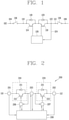
- FIG. 1 illustrates an example of a configuration of a power switching system in which a plurality of power devices are connected in series.
- a typical power switching system may include a first terminal 110, a second terminal 112, a first semiconductor element 114, a second semiconductor element 116, diodes 118 and 120 connected to the first semiconductor element 114 and the second semiconductor element 116, and a control unit 126.
- the first semiconductor element 114 and the second semiconductor element 116 may be respectively connected to the first diode 118 and the second diode 120 to constitute different power devices.
- the first semiconductor element 114 and the second semiconductor element 116 may control a flow of current from the first terminal 110 to the second terminal 112 or from the second terminal 112 to the first terminal 110.
- the control unit 126 may apply a voltage signal to each of the first semiconductor element 114 and the second semiconductor element 116, to turn on or off the first power device constituted by the first sem iconductor element 114 and the second power device 220 constituted by the second semiconductor element 116.
- the power switching system 108 may include a first disconnector 136 electrically connected between the first terminal 110 and a first bus section 104, and a second disconnector 138 electrically connected between the second terminal 112 and a second bus section 106.
- the disconnectors 136 and 138 may be closed in a normal operation, thereby providing an electrical connection between the individual bus sections and terminals.
- the disconnectors 136 and 138 may be opened for the purpose of maintenance and the like, and in this case, the power switching system 108 may be disconnected from a power distribution bus 102.
- the power switching system 108 may include a current sensor 122 provided between the first disconnector 136 and the first semiconductor element 114 or between the second disconnector 138 and the second semiconductor element 116. Accordingly, the control unit 126 may monitor currents flowing along the first power device and the second power device based on current values measured by the current sensor 122.
- the present disclosure is directed to solving aforementioned problems and other drawbacks, and one aspect of the present disclosure is to provide a monitoring system and method, capable of determining a fault for each power device that constitutes a power switching system.
- Another aspect of the present disclosure is to provide a monitoring system and method, capable of detecting whether a fault state has occurred due to an introduction of an external current or due to a defect of a power device constituting a power switching system when the fault state is detected in the power switching system.
- a power device monitoring system may include a first power device and a second power device each including a semiconductor element, a first sensor and a second sensor connected to the first and second power devices, respectively, the first sensor sensing information related to a first current flowing through the first power device and the second sensor sensing information related to a second current flowing through the second power device, a third sensor to sense information related to a third current flowing between the first power device and the second power device, and a control unit to compare the first current and the second current with the third current, and determine a fault state for each power device according to a difference between the first and second currents and the third current.
- the first sensor and the second sensor each may further include a temperature sensor.
- the temperature sensor may measure a temperature of the first power device or the second power device, and current related information regarding a current flowing through the first power device or the second power device and information related to the measured temperature may be transmitted to the control unit.
- control unit may correct the current-related information based on the temperature information.
- control unit may perform the correction for each power device based on a table modeling a relationship between temperature and current according to a characteristic of each power device, and detect the first current or the second current.
- control unit may perform the correction for each power device based on a table modeling a relationship between temperature and voltage according to a characteristic of each power device, and detect the first current or the second current.
- the first power device and the second power device each may be configured as an insulated gate bipolar transistor (IGBT).
- the first current may be a current flowing between a drain terminal and a source terminal of the first power device
- the second current may be a current between a drain terminal and a source terminal of the second power device.
- any one of the first sensor and the second sensor may be a sensor having higher accuracy and reliability than another one.
- a power device monitoring method in a power switching system may include a first power device and a second power device each including a semiconductor element.
- the method may include a first step of sensing current-related information regarding a first current flowing through the first power device, a second current flowing through the second power device, and a third current flowing between the first power device and the second power device, a second step of detecting the first current, the second current, and the third current based on the current-related information, a third step of setting the third current as a reference current, a fourth step of comparing the reference current with the first current and the second current, and a fifth step of determining a state of the first power device and a state of the second power device according to a result of the comparison.
- the information related to the first current and the information related to the second current may further include a temperature of the first power device and a temperature of the second power device, respectively.
- the second step may further include a 2-1th step of correcting the information related to the first current according to the temperature of the first power device and the information related to the second current according to the temperature of the second power device.
- the 2-1th step may be configured to perform the correction for each power device based on a table modeling a relationship between temperature and current or a table modeling a relationship between temperature and voltage according to a characteristic of each power device.
- the fifth step may further include a 5-1th step of determining whether differences between the reference current and the first and second currents are within a preset allowable error range, and a 5-2th step of differently determining, when the differences from the reference current exceed the allowable error range, the state of the first power device corresponding to the first current and the state of the second power device corresponding to the second current, according to whether the first and second currents are greater or smaller than the reference current.
- the 5-2th step may be configured to determine, when any one of the first current or the second current is greater than the reference current, that an external current has been introduced into the first power device or the second power device corresponding to the one current.
- the fifth step may further include a 5-3th step of determining, when any one of the first current or the second current is smaller than the reference current, that a damage or failure has occurred in the first power device or the second power device corresponding to the one current.
- the method may further include a sixth step of determining whether a preset period has expired, and a seventh step of repetitively performing the first step to the fifth step according to whether the preset period has expired.
- the first power device and the second power device each may be configured as an insulated gate bipolar transistor (IGBT).
- the first current may be a current flowing between a drain terminal and a source terminal of the first power device
- the second current may be a current between a drain terminal and a source terminal of the second power device.
- a current can be measured for each power device constituting a power switching system, thereby determining presence or absence of a fault for each power device.
- a current flowing through each power device can be compared with a current flowing between the power devices, thereby determining presence or absence of a fault for each power device.
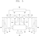
- FIG. 2 is a diagram illustrating a configuration of a monitoring system for monitoring a state of each power device 200 in accordance with an implementation of the present disclosure, in a power switching system.
- a power device monitoring system 200 may include a first power device 210, a second power device 220, a first sensor 201 for sensing a current flowing through the first power device 210, a second sensor 202 for sensing a current flowing through the second power device 220, a third sensor 203 for sensing a current flowing between the first power device 210 and the second power device 220, a first driving unit 206 for controlling ON or OFF of the first power device 210, a second driving unit 207 for controlling ON or OFF of the second power device 220, and a control unit 208 for controlling the operations of the first driving unit 206 and the second driving unit 207.
- the first power device 210 may include a first semiconductor element 212 and a first diode 211.
- the first semiconductor element 212 may be configured as an insulated gate bipolar transistor (IGBT).
- the first power device 210 may be turned on (ON state) when a preset voltage is applied by the first driving unit 206. In the ON state, a current may flow through the first semiconductor element 212. On the other hand, the first power device 210 may be turned off when the preset voltage is not applied by the first driving unit 206. In the OFF state, a current may flow through the first diode 211.
- the second power device 220 may include a second semiconductor element 222 and a second diode 221.
- the second semiconductor element 222 may be configured as an insulated gate bipolar transistor (IGBT).
- the second power device 220 may be turned on (ON state) when a preset voltage is applied by the second driving unit 207. In the ON state, a current may flow through the second semiconductor element 222. On the other hand, the second power device 210 may be turned off when the preset voltage is not applied by the second driving unit 207. In the OFF state, a current may flow through the second diode 221.
- the first sensor 201 may be a sensor for directly or indirectly measuring a current flowing through the first power device 210.
- the first sensor 201 may be a sensor (e.g., a hall sensor) that is directly connected to the first power device 210 to directly measure a first current flowing through the first power device 210.
- the first sensor may be a voltage sensor that includes a preset resistance for indirectly measuring the first current.
- a voltage measured by the first sensor 201 may be a voltage (i.e., Voltage drain to source (VDS)) between a drain terminal and a source terminal in the first semiconductor element 212 of the first power device 210.
- the first current may be a current that flows between the drain terminal and the source terminal in the first semiconductor element 212.
- the second sensor 202 may be a sensor for directly or indirectly measuring a current flowing through the second power device 220.
- the second sensor 202 may be a current sensor that directly measure a second current flowing through the second power device 220, or a voltage sensor that includes a preset resistance for indirectly measuring the first current.
- a voltage measured by the second sensor 202 may be a voltage (i.e., Voltage drain to source (VDS)) between a drain terminal and a source terminal in the second semiconductor element 222 of the second power device 220.
- the second current may be a current that flows between the drain terminal and the source terminal in the second semiconductor element 222.
- the third sensor 203 may be a sensor for directly or indirectly measuring a current flowing between the first power device 210 and the second power device 220.
- the third sensor 203 may be disposed on a connection wire for connecting the first power device 210 and the second power device 220, and may be a sensor for directly measuring a current flowing through the connection wire or a voltage sensor including a preset resistance.
- the first driving unit 206 and the second driving unit 207 may apply a preset driving voltage to at least one of the first power device 210 and the second power device 220 under the control of the control unit 208. In this case, a different driving voltage may be applied to the first power device 210 or the second power device 220.
- the control unit 208 may measure the first current flowing through the first power device 210 and the second current flowing through the second power device 220 based on measurement results of the first sensor 201 and the second sensor 202.
- the control unit 208 may determine the first current flowing through the first power device 210 and the second current flowing through the second power device 220 based the measurement result of the first sensor 201 and the measurement result of the second sensor 202.
- the control unit 208 may detect the first current and the second current based on a current-voltage table modeling a current-voltage relationship according to a characteristic of each power device.
- control unit 208 may measure a third current flowing between the first power device 210 and the second power device 220 based on a measurement value of the third sensor 203.
- the control unit 208 may directly detect the third current flowing between the first power device 210 and the second power device 220 based on the current value measured by the third sensor 203.
- the third sensor 203 is a voltage sensor
- the third current may be detected based on a table modeling a voltage-current relationship according to a preset resistance.
- control unit 208 may set the third current as a reference current.
- the set reference current may be compared with the first and second currents.
- the control unit 208 may determine that a fault has occurred. In this case, the control unit 208 may detect a power device with the fault based on the current out of the allowable error range.
- the control unit 208 may detect that a fault has occurred in the first power device 210.
- the control unit 208 may detect that a fault has occurred in the second power device 220.
- the control unit 208 may determine that there is another current flowing into the first power device or the second power device 220. That is, the control unit 208 may determine that an external current such as a leakage current flows into the first power device 210 or the second power device 220.
- control unit 208 may determine that a defect or damage has occurred in the first power device or the second power device 220.
- first sensor 201 and the second sensor 202 are respectively connected to the power devices, errors may occur due to heat generated by the connected power devices.
- the control unit 208 may correct (compensate for) the error based on a preset temperature-current table or a temperature-voltage table.
- the first sensor 201 and the second sensor 202 each may further include a temperature sensor, and may transmit current values or voltage values measured from the respective power devices and temperature values measured by the temperature sensors to the control unit 208 when the first current and the second current are sensed.
- control unit 208 may include a table modeling a relationship between temperature and current according to a characteristic of each power device or a table modeling a relationship between temperature and voltage according to a characteristic of each power device. Further, the control unit may correct information (current value or voltage value) measured by the first sensor 201 and information (current value or voltage value) measured by the second sensor 202 based on the provided modeling table.
- first sensor 201 and the second sensor 202 may be connected to the first power device 210 and the second power device 220, respectively, while the third sensor 203 may be provided on the connection wire connecting the first power device 210 and the second power device 220.
- heat generated from the first power device 210 and the second power device 220 may be directly transferred to the first sensor 201 and the second sensor 202 and errors caused due to the heat may be included in the measured results of the first sensor 201 and the second sensor 202.
- heat of each power device may not be transferred to the third sensor 203 and thus an error caused due to the heat (i.e., temperature error) may be smaller than those in the first sensor 201 and the second sensor 202.
- the third sensor 203 can measure a more accurate current than the first sensor 201 and the second sensor 202. Therefore, the control unit 208 can set the third current measured by the third sensor 203 as a reference current value.
- FIG. 3 is a flowchart illustrating processes of determining a state of each power device according to a measurement result of each sensor in a power monitoring system in accordance with a first implementation of the present disclosure.
- the control unit 208 of the power monitoring system may first receive measurement results from the first sensor 201, the second sensor 202, and the third sensor 203, respectively (S300).
- the first sensor 201 to the third sensor 203 may be voltage sensors each including a preset voltage, or current sensors that directly sense current values.
- the control unit 208 may measure a first current flowing through the first power device 210 and a second current flowing through the second power device based on the measurement results of the first sensor 201 and the second sensor 202 (S302).
- the first sensor 201 and the second sensor 202 are voltage sensors
- the first current and the second current may be measured by a voltage-current table modeling a voltage change with respect to a current according to a characteristic of each power device.
- the first sensor 201 and the second sensor 202 are temperature sensors
- the first current and the second current may be measured by a temperature-current table modeling a temperature change with respect to a current according to the characteristic of each power device.
- each of the first sensor 201 and the second sensor 202 may further include a temperature sensor.
- the first sensor 201 and the second sensor 202 may further transmit temperature values sensed through the temperature sensors when the current values or voltage values of the first power device 210 and the second power device 220 are sensed.
- the control unit 208 may then compensate for (correct) information (current value or voltage value) sensed by the first sensor 201 and information (current value or voltage value) sensed by the second sensor 202, based on the transmitted temperature values of the first power device 210 and the second power device 220.
- the control unit 208 may measure a third current flowing between the first power device 210 and the second power device 220 based on a measurement result of the third sensor 203 (S304).
- the third sensor 203 is a current sensor
- the third current may be directly measured based on the measured value.
- the third sensor 203 is a voltage sensor
- the third current may be detected based on a voltage-current table according to a preset voltage.
- the control unit 208 may compare the first current and the second current with the detected third current (S306). In the step S306, the control unit 208 may determine whether the first current or the second current is large or small than a reference current, that is, the third current, and detect whether a difference between the third current and the first current or the second current is within a preset allowable error range.
- the control unit 208 may determine states of the first power device 210 and the second power device 220, respectively, according to a result of the comparison of the step S306 (S308).
- the control unit 208 may determine that an external current has been introduced into the first power device 210.
- the control unit 208 may determine that the first power device 210 has been deteriorated due to damage or failure.
- control unit 208 may determine that an external current has been introduced into the second power device 220.
- the control unit 208 may determine that the second power device 220 has been deteriorated due to damage or failure.
- control unit 208 may determine the states of the first power device and the second power device differently according to whether the first current or the second current is smaller or larger than the reference current. Also, the control unit 208 may determine the states of the first power device and the second power device individually.
- each power device when the same current continuously flows, the two power devices may exhibit characteristics according to a flowing direction of the current.
- Each power device may have a specific characteristic value depending on a current flowing in a forward or reverse direction.
- the characteristic of the power device over a specific range may be expressed as a ratio of V/I, and if a current flowing even in any one of the forward direction and the reverse direction exceeds the range or ratio of the characteristic value, it may be determined that the power device has been damaged.
- control unit 208 may immediately notify it to an upper system and stop the operation of each power device. In this case, in order to stop the operation, the control unit 208 may set the order of stopping the operation of each component (e.g., each power device) in consideration of system stability.
- control unit 208 may monitor (check) the states of the power devices through a continuous operation check repetitively at a preset period during the operation of the system, and determine the states of the respective power devices. Accordingly, reliability of the system can be improved.
- FIG. 4 (a) and (b) are diagrams illustrating configurations of a power device monitoring system in accordance with a second implementation of the present disclosure.
- a power device 400 may be an integrated power device that can perform bidirectional control of currents according to a flow of current, namely, can control a current flowing in a forward direction and a current flowing in a reverse direction.
- the power device 400 may be turned on or off by a single driving unit 440.
- the driving unit 440 may apply voltages to a first semiconductor element 405 and a second semiconductor element 406, respectively, to operate the first semiconductor element 405 and the second semiconductor element 406 under the control of the control unit 450.
- the power device 400 may include two semiconductor elements 405 and 406 and two diodes 401 and 402.
- a first sensor 410 and a second sensor 420 may sense information (current value or voltage value) related to a first current flowing through the first semiconductor element 405 and information (current value or voltage value) related to a second current flowing through the second semiconductor element 406.
- the first sensor 410 may sense information related to a current (first current) flowing between a drain terminal and a source terminal of the first semiconductor element 405
- the second sensor 420 may sense information related to a current (second current) flowing between a drain terminal and a source terminal of the second semiconductor element 406.
- the power device monitoring system may further include a third sensor 430 that is disposed between the first semiconductor element 405 and the second semiconductor element 406 to sense information (voltage value or current value) related to a current flowing between the first semiconductor element 405 and the second semiconductor element 406.
- a third sensor 430 that is disposed between the first semiconductor element 405 and the second semiconductor element 406 to sense information (voltage value or current value) related to a current flowing between the first semiconductor element 405 and the second semiconductor element 406.
- information measured by the first sensor 410 and the second sensor 420 may be transmitted to the control unit 450.
- information measured by the third sensor 430 may be transmitted to the control unit 450 through the driving unit 440.
- the control unit 450 may detect the first current, the second current, and the third current based on the information measured by each of the first sensor 410 to the third sensor 430, and determine whether or not a fault has occurred in the power device 400 based on a comparison result between the third current as a reference current and the first and second currents.
- control unit 450 may also detect a semiconductor element, in which a fault has occurred of the semiconductor elements constituting the power device 400, according to a result of the comparison between the third current and the first and second currents.
- any one of the first sensor 410 and the second sensor 420 may be implemented as a more precise and more reliable sensor than the other.
- a current or voltage flowing through the power device 400 may be measured and a direction of the current may be predicted through the more precise and more reliable sensor, and the measured and predicted results may be compared with a measurement result of the other sensor, thereby monitoring stability of the power device 400.
- FIG. 5 is a diagram illustrating a configuration of a power device monitoring system in accordance with a third implementation of the present disclosure.
- the present disclosure may further include overvoltage protection units 500 for protecting power devices 210 and 220 from overvoltage.
- the overvoltage protection units 500 each may include at least one of a metal oxide varistor (MOV) and a snubber.
- MOV metal oxide varistor
- the overvoltage protection unit 500 may be disposed at both ends with respect to the power devices 210 and 220.
- resistors 510 and voltage sensors 521 and 522 may be connected in series at the both ends with respect to the power devices 210 and 220.
- the serially-connected resistors and voltage sensors 521 and 522 may measure voltages of currents input to the respective power devices 210 and 220.
- Each of the voltage sensors 521 and 522 may include an insulating interface and an analog digital converter (ADC) for measuring an analog voltage as a digital value.
- ADC analog digital converter
- the insulating interface may prevent the voltages measured by the voltage sensors 521 and 522 from being applied to the control unit 280.
- a communication interface 530 may be further provided, and an external input may be applied to the control unit 208 through the communication interface 530. Also, the control unit 208 may exchange information with other external devices through the communication interface 530.
- each power device includes a diode
- a diode may not be included depending on type and characteristic of a power device.
- each power device has a configuration including a semiconductor element implemented as an insulated gate bipolar transistor (IGBT), but the present disclosure may, of course, be applied even to a case including other types of semiconductor elements.
- the present disclosure can also be applied to other power semiconductor devices or power devices such as SiC or GaN devices.
- the present disclosure can be implemented as computer-readable codes in a program-recorded medium.
- the computer-readable medium may include all types of recording devices each storing data readable by a computer system. Examples of such computer-readable media may include hard disk drive (HDD), solid state disk (SSD), silicon disk drive (SDD), ROM, RAM, CD-ROM, magnetic tape, floppy disk, optical data storage element and the like. Also, the computer-readable medium may also be implemented as a format of carrier wave (e.g., transmission via an Internet).
- the computer may include the control unit 208. Therefore, the detailed description should not be limitedly construed in all of the aspects, and should be understood to be illustrative. Therefore, all changes and modifications that fall within the metes and bounds of the claims, or equivalents of such metes and bounds are therefore intended to be embraced by the appended claims.
Landscapes
- Physics & Mathematics (AREA)
- General Physics & Mathematics (AREA)
- Engineering & Computer Science (AREA)
- Power Engineering (AREA)
- Microelectronics & Electronic Packaging (AREA)
- Power Conversion In General (AREA)
- Electronic Switches (AREA)
- Inverter Devices (AREA)
Abstract
Description
- The present disclosure relates to a monitoring system for a plurality of power devices serially connected in a main circuit of a current transmission path.
- In general, in an inverter and a semiconductor-based circuit breaker, power in a power distribution bus is switched through a power switching system in which power devices including semiconductor elements are connected in series in a main circuit of a current transmission path.
-
FIG. 1 illustrates an example of a configuration of a power switching system in which a plurality of power devices are connected in series. - Referring to
FIG. 1 , a typical power switching system may include afirst terminal 110, asecond terminal 112, afirst semiconductor element 114, asecond semiconductor element 116,diodes first semiconductor element 114 and thesecond semiconductor element 116, and acontrol unit 126. Here, thefirst semiconductor element 114 and thesecond semiconductor element 116 may be respectively connected to thefirst diode 118 and thesecond diode 120 to constitute different power devices. - The
first semiconductor element 114 and thesecond semiconductor element 116 may control a flow of current from thefirst terminal 110 to thesecond terminal 112 or from thesecond terminal 112 to thefirst terminal 110. - The
control unit 126 may apply a voltage signal to each of thefirst semiconductor element 114 and thesecond semiconductor element 116, to turn on or off the first power device constituted by the firstsem iconductor element 114 and thesecond power device 220 constituted by thesecond semiconductor element 116. - Meanwhile, the power switching system 108 may include a
first disconnector 136 electrically connected between thefirst terminal 110 and afirst bus section 104, and asecond disconnector 138 electrically connected between thesecond terminal 112 and asecond bus section 106. Thedisconnectors disconnectors power distribution bus 102. - The power switching system 108 may include a
current sensor 122 provided between thefirst disconnector 136 and thefirst semiconductor element 114 or between thesecond disconnector 138 and thesecond semiconductor element 116. Accordingly, thecontrol unit 126 may monitor currents flowing along the first power device and the second power device based on current values measured by thecurrent sensor 122. - On the other hand, in this power switching system, when a fault (abnormal) state is detected from a current measurement result of the
current sensor 122, there is not any method to determine whether the detected fault state is caused due to an introduction of an external current or due to damage to a power semiconductor or circuit inside the power switching system. As a result, there is a problem in that it is impossible to accurately determine whether such fault has occurred in the power semiconductor constituting the power device or in an internal circuit of the power switching system. - The present disclosure is directed to solving aforementioned problems and other drawbacks, and one aspect of the present disclosure is to provide a monitoring system and method, capable of determining a fault for each power device that constitutes a power switching system.
- Another aspect of the present disclosure is to provide a monitoring system and method, capable of detecting whether a fault state has occurred due to an introduction of an external current or due to a defect of a power device constituting a power switching system when the fault state is detected in the power switching system.
- In order to achieve these and other advantages and in accordance with the purpose of this specification, as embodied and broadly described herein, there is provided a power device monitoring system that may include a first power device and a second power device each including a semiconductor element, a first sensor and a second sensor connected to the first and second power devices, respectively, the first sensor sensing information related to a first current flowing through the first power device and the second sensor sensing information related to a second current flowing through the second power device, a third sensor to sense information related to a third current flowing between the first power device and the second power device, and a control unit to compare the first current and the second current with the third current, and determine a fault state for each power device according to a difference between the first and second currents and the third current.
- In one implementation, the first sensor and the second sensor each may further include a temperature sensor. The temperature sensor may measure a temperature of the first power device or the second power device, and current related information regarding a current flowing through the first power device or the second power device and information related to the measured temperature may be transmitted to the control unit.
- In one implementation, when the current-related information and the temperature information are received from at least one of the first sensor and the second sensor, the control unit may correct the current-related information based on the temperature information.
- In one implementation, the control unit may perform the correction for each power device based on a table modeling a relationship between temperature and current according to a characteristic of each power device, and detect the first current or the second current.
- In one implementation, the control unit may perform the correction for each power device based on a table modeling a relationship between temperature and voltage according to a characteristic of each power device, and detect the first current or the second current.
- In one implementation, the first power device and the second power device each may be configured as an insulated gate bipolar transistor (IGBT). The first current may be a current flowing between a drain terminal and a source terminal of the first power device, and the second current may be a current between a drain terminal and a source terminal of the second power device.
- In one implementation, any one of the first sensor and the second sensor may be a sensor having higher accuracy and reliability than another one.
- In order to achieve these and other advantages and in accordance with the purpose of this specification, as embodied and broadly described herein, there is provided a power device monitoring method in a power switching system that may include a first power device and a second power device each including a semiconductor element. The method may include a first step of sensing current-related information regarding a first current flowing through the first power device, a second current flowing through the second power device, and a third current flowing between the first power device and the second power device, a second step of detecting the first current, the second current, and the third current based on the current-related information, a third step of setting the third current as a reference current, a fourth step of comparing the reference current with the first current and the second current, and a fifth step of determining a state of the first power device and a state of the second power device according to a result of the comparison.
- In one implementation, the information related to the first current and the information related to the second current may further include a temperature of the first power device and a temperature of the second power device, respectively. The second step may further include a 2-1th step of correcting the information related to the first current according to the temperature of the first power device and the information related to the second current according to the temperature of the second power device.
- In one implementation, the 2-1th step may be configured to perform the correction for each power device based on a table modeling a relationship between temperature and current or a table modeling a relationship between temperature and voltage according to a characteristic of each power device.
- In one implementation, the fifth step may further include a 5-1th step of determining whether differences between the reference current and the first and second currents are within a preset allowable error range, and a 5-2th step of differently determining, when the differences from the reference current exceed the allowable error range, the state of the first power device corresponding to the first current and the state of the second power device corresponding to the second current, according to whether the first and second currents are greater or smaller than the reference current.
- In one implementation, the 5-2th step may be configured to determine, when any one of the first current or the second current is greater than the reference current, that an external current has been introduced into the first power device or the second power device corresponding to the one current.
- In one implementation, the fifth step may further include a 5-3th step of determining, when any one of the first current or the second current is smaller than the reference current, that a damage or failure has occurred in the first power device or the second power device corresponding to the one current.
- In one implementation, the method may further include a sixth step of determining whether a preset period has expired, and a seventh step of repetitively performing the first step to the fifth step according to whether the preset period has expired.
- In one implementation, the first power device and the second power device each may be configured as an insulated gate bipolar transistor (IGBT). The first current may be a current flowing between a drain terminal and a source terminal of the first power device, and the second current may be a current between a drain terminal and a source terminal of the second power device.
- According to at least one of implementations of the present disclosure, a current can be measured for each power device constituting a power switching system, thereby determining presence or absence of a fault for each power device.
- According to at least one of the implementations of the present disclosure, a current flowing through each power device can be compared with a current flowing between the power devices, thereby determining presence or absence of a fault for each power device.
-
-
FIG. 1 is an exemplarily view illustrating a configuration of a typical power switching system in which a plurality of power devices are connected in series. -
FIG. 2 is a diagram illustrating a configuration of a monitoring system for monitoring a state of each power device in accordance with an implementation of the present disclosure, in a power switching system. -
FIG. 3 is a flowchart illustrating processes of determining a state of each power device according to a measurement result of each sensor in a power monitoring system in accordance with a first implementation of the present disclosure. -
FIG. 4 (a) and (b) are diagrams illustrating configurations of a power device monitoring system in accordance with a second implementation of the present disclosure. -
FIG. 5 is a diagram illustrating a configuration of a power device monitoring system in accordance with a third implementation of the present disclosure. - It is noted that the technical terms used herein are used only to describe specific implementations and are not intended to limit the invention. A singular representation used herein may include a plural representation unless it represents a definitely different meaning from the context. In this specification, the terms "comprising" and "including" should not be construed to necessarily include all of the elements or steps disclosed herein, and should be construed not to include some of the elements or steps thereof, or should be construed to further include additional elements or steps.
- In describing the technology disclosed in this specification, if a detailed explanation for a related known function or construction is considered to unnecessarily divert the gist of the present disclosure, such explanation has been omitted but would be understood by those skilled in the art.
- Hereinafter, implementations disclosed herein will be described in detail with reference to the accompanying drawings.
-
FIG. 2 is a diagram illustrating a configuration of a monitoring system for monitoring a state of eachpower device 200 in accordance with an implementation of the present disclosure, in a power switching system. - Referring to
FIG. 2 , a powerdevice monitoring system 200 according to an implementation of the present disclosure may include afirst power device 210, asecond power device 220, afirst sensor 201 for sensing a current flowing through thefirst power device 210, asecond sensor 202 for sensing a current flowing through thesecond power device 220, athird sensor 203 for sensing a current flowing between thefirst power device 210 and thesecond power device 220, afirst driving unit 206 for controlling ON or OFF of thefirst power device 210, asecond driving unit 207 for controlling ON or OFF of thesecond power device 220, and acontrol unit 208 for controlling the operations of thefirst driving unit 206 and thesecond driving unit 207. - First, the
first power device 210 may include afirst semiconductor element 212 and afirst diode 211. Here, thefirst semiconductor element 212 may be configured as an insulated gate bipolar transistor (IGBT). - The
first power device 210 may be turned on (ON state) when a preset voltage is applied by thefirst driving unit 206. In the ON state, a current may flow through thefirst semiconductor element 212. On the other hand, thefirst power device 210 may be turned off when the preset voltage is not applied by thefirst driving unit 206. In the OFF state, a current may flow through thefirst diode 211. - Similarly, the
second power device 220 may include asecond semiconductor element 222 and asecond diode 221. Here, thesecond semiconductor element 222 may be configured as an insulated gate bipolar transistor (IGBT). - The
second power device 220 may be turned on (ON state) when a preset voltage is applied by thesecond driving unit 207. In the ON state, a current may flow through thesecond semiconductor element 222. On the other hand, thesecond power device 210 may be turned off when the preset voltage is not applied by thesecond driving unit 207. In the OFF state, a current may flow through thesecond diode 221. - Meanwhile, the
first sensor 201 may be a sensor for directly or indirectly measuring a current flowing through thefirst power device 210. For example, thefirst sensor 201 may be a sensor (e.g., a hall sensor) that is directly connected to thefirst power device 210 to directly measure a first current flowing through thefirst power device 210. Alternatively, the first sensor may be a voltage sensor that includes a preset resistance for indirectly measuring the first current. - Here, a voltage measured by the
first sensor 201 may be a voltage (i.e., Voltage drain to source (VDS)) between a drain terminal and a source terminal in thefirst semiconductor element 212 of thefirst power device 210. In this case, the first current may be a current that flows between the drain terminal and the source terminal in thefirst semiconductor element 212. - Similarly, the
second sensor 202 may be a sensor for directly or indirectly measuring a current flowing through thesecond power device 220. For example, thesecond sensor 202 may be a current sensor that directly measure a second current flowing through thesecond power device 220, or a voltage sensor that includes a preset resistance for indirectly measuring the first current. - Here, a voltage measured by the
second sensor 202 may be a voltage (i.e., Voltage drain to source (VDS)) between a drain terminal and a source terminal in thesecond semiconductor element 222 of thesecond power device 220. In this case, the second current may be a current that flows between the drain terminal and the source terminal in thesecond semiconductor element 222. - The
third sensor 203 may be a sensor for directly or indirectly measuring a current flowing between thefirst power device 210 and thesecond power device 220. For example, thethird sensor 203 may be disposed on a connection wire for connecting thefirst power device 210 and thesecond power device 220, and may be a sensor for directly measuring a current flowing through the connection wire or a voltage sensor including a preset resistance. - Meanwhile, the
first driving unit 206 and thesecond driving unit 207 may apply a preset driving voltage to at least one of thefirst power device 210 and thesecond power device 220 under the control of thecontrol unit 208. In this case, a different driving voltage may be applied to thefirst power device 210 or thesecond power device 220. - The
control unit 208 may measure the first current flowing through thefirst power device 210 and the second current flowing through thesecond power device 220 based on measurement results of thefirst sensor 201 and thesecond sensor 202. - For example, when the
first sensor 201 and thesecond sensor 202 are current sensors, thecontrol unit 208 may determine the first current flowing through thefirst power device 210 and the second current flowing through thesecond power device 220 based the measurement result of thefirst sensor 201 and the measurement result of thesecond sensor 202. - However, when the
first sensor 201 and thesecond sensor 202 are voltage sensors, thecontrol unit 208 may detect the first current and the second current based on a current-voltage table modeling a current-voltage relationship according to a characteristic of each power device. - In addition, the
control unit 208 may measure a third current flowing between thefirst power device 210 and thesecond power device 220 based on a measurement value of thethird sensor 203. In this case, when thethird sensor 203 is a current sensor, thecontrol unit 208 may directly detect the third current flowing between thefirst power device 210 and thesecond power device 220 based on the current value measured by thethird sensor 203. However, when thethird sensor 203 is a voltage sensor, the third current may be detected based on a table modeling a voltage-current relationship according to a preset resistance. - Then, the
control unit 208 may set the third current as a reference current. In addition, the set reference current may be compared with the first and second currents. As a result of the comparison, when there is a current, of the first current or the second current, having a difference from the third current which is out of a preset allowable error range, thecontrol unit 208 may determine that a fault has occurred. In this case, thecontrol unit 208 may detect a power device with the fault based on the current out of the allowable error range. - In this case, when a difference between the first current and the reference current exceeds the allowable error range, the
control unit 208 may detect that a fault has occurred in thefirst power device 210. On the other hand, when a difference between the second current and the reference current exceeds the allowable error range, thecontrol unit 208 may detect that a fault has occurred in thesecond power device 220. - In more detail, when the first current or the second current is greater than the reference current (third current) and the difference from the reference current exceeds the allowable error range, the
control unit 208 may determine that there is another current flowing into the first power device or thesecond power device 220. That is, thecontrol unit 208 may determine that an external current such as a leakage current flows into thefirst power device 210 or thesecond power device 220. - On the other hand, when the first current or the second current is smaller than the reference current (third current) and the difference from the reference current exceeds the allowable error range, the
control unit 208 may determine that a defect or damage has occurred in the first power device or thesecond power device 220. - Meanwhile, since the
first sensor 201 and thesecond sensor 202 are respectively connected to the power devices, errors may occur due to heat generated by the connected power devices. - In order to prevent such error caused by a temperature difference, the
control unit 208 may correct (compensate for) the error based on a preset temperature-current table or a temperature-voltage table. To this end, thefirst sensor 201 and thesecond sensor 202 each may further include a temperature sensor, and may transmit current values or voltage values measured from the respective power devices and temperature values measured by the temperature sensors to thecontrol unit 208 when the first current and the second current are sensed. - Also, for each power device, the
control unit 208 may include a table modeling a relationship between temperature and current according to a characteristic of each power device or a table modeling a relationship between temperature and voltage according to a characteristic of each power device. Further, the control unit may correct information (current value or voltage value) measured by thefirst sensor 201 and information (current value or voltage value) measured by thesecond sensor 202 based on the provided modeling table. - On the other hand, the
first sensor 201 and thesecond sensor 202 may be connected to thefirst power device 210 and thesecond power device 220, respectively, while thethird sensor 203 may be provided on the connection wire connecting thefirst power device 210 and thesecond power device 220. - Accordingly, heat generated from the
first power device 210 and thesecond power device 220 may be directly transferred to thefirst sensor 201 and thesecond sensor 202 and errors caused due to the heat may be included in the measured results of thefirst sensor 201 and thesecond sensor 202. On the other hand, heat of each power device may not be transferred to thethird sensor 203 and thus an error caused due to the heat (i.e., temperature error) may be smaller than those in thefirst sensor 201 and thesecond sensor 202. - Accordingly, the
third sensor 203 can measure a more accurate current than thefirst sensor 201 and thesecond sensor 202. Therefore, thecontrol unit 208 can set the third current measured by thethird sensor 203 as a reference current value. -
FIG. 3 is a flowchart illustrating processes of determining a state of each power device according to a measurement result of each sensor in a power monitoring system in accordance with a first implementation of the present disclosure. - Referring to
FIG. 3 , thecontrol unit 208 of the power monitoring system according to an implementation of the present disclosure may first receive measurement results from thefirst sensor 201, thesecond sensor 202, and thethird sensor 203, respectively (S300). Here, thefirst sensor 201 to thethird sensor 203 may be voltage sensors each including a preset voltage, or current sensors that directly sense current values. - When measurement results of the respective sensors are obtained, the
control unit 208 may measure a first current flowing through thefirst power device 210 and a second current flowing through the second power device based on the measurement results of thefirst sensor 201 and the second sensor 202 (S302). In this case, when thefirst sensor 201 and thesecond sensor 202 are voltage sensors, the first current and the second current may be measured by a voltage-current table modeling a voltage change with respect to a current according to a characteristic of each power device. On the other hand, when thefirst sensor 201 and thesecond sensor 202 are temperature sensors, the first current and the second current may be measured by a temperature-current table modeling a temperature change with respect to a current according to the characteristic of each power device. - Meanwhile, each of the
first sensor 201 and thesecond sensor 202 may further include a temperature sensor. In this case, thefirst sensor 201 and thesecond sensor 202 may further transmit temperature values sensed through the temperature sensors when the current values or voltage values of thefirst power device 210 and thesecond power device 220 are sensed. Thecontrol unit 208 may then compensate for (correct) information (current value or voltage value) sensed by thefirst sensor 201 and information (current value or voltage value) sensed by thesecond sensor 202, based on the transmitted temperature values of thefirst power device 210 and thesecond power device 220. - The
control unit 208 may measure a third current flowing between thefirst power device 210 and thesecond power device 220 based on a measurement result of the third sensor 203 (S304). In this case, when thethird sensor 203 is a current sensor, the third current may be directly measured based on the measured value. However, when thethird sensor 203 is a voltage sensor, the third current may be detected based on a voltage-current table according to a preset voltage. - When the third current is detected, the
control unit 208 may compare the first current and the second current with the detected third current (S306). In the step S306, thecontrol unit 208 may determine whether the first current or the second current is large or small than a reference current, that is, the third current, and detect whether a difference between the third current and the first current or the second current is within a preset allowable error range. - The
control unit 208 may determine states of thefirst power device 210 and thesecond power device 220, respectively, according to a result of the comparison of the step S306 (S308). - For example, when the first current is greater than the third current and a difference between the currents exceeds the preset allowable error range, the
control unit 208 may determine that an external current has been introduced into thefirst power device 210. Alternatively, when the first current is smaller than the third current and a difference between the currents exceeds the preset allowable error range, thecontrol unit 208 may determine that thefirst power device 210 has been deteriorated due to damage or failure. - Also, when the second current is greater than the third current and a difference between the currents exceeds the preset allowable error range, the
control unit 208 may determine that an external current has been introduced into thesecond power device 220. Alternatively, when the second current is smaller than the third current and a difference between the currents exceeds the preset allowable error range, thecontrol unit 208 may determine that thesecond power device 220 has been deteriorated due to damage or failure. - That is, when the difference between the reference current (third current) and the first current or the second current exceeds the allowable error range, the
control unit 208 may determine the states of the first power device and the second power device differently according to whether the first current or the second current is smaller or larger than the reference current. Also, thecontrol unit 208 may determine the states of the first power device and the second power device individually. - On the other hand, assuming that each power device has the same performance, when the same current continuously flows, the two power devices may exhibit characteristics according to a flowing direction of the current. Each power device may have a specific characteristic value depending on a current flowing in a forward or reverse direction. In this case, the characteristic of the power device over a specific range may be expressed as a ratio of V/I, and if a current flowing even in any one of the forward direction and the reverse direction exceeds the range or ratio of the characteristic value, it may be determined that the power device has been damaged.
- In addition, when it is determined that the power device has been damaged, the
control unit 208 may immediately notify it to an upper system and stop the operation of each power device. In this case, in order to stop the operation, thecontrol unit 208 may set the order of stopping the operation of each component (e.g., each power device) in consideration of system stability. - Meanwhile, the steps of
FIG. 3 may be performed during an initial check process for an initial system operation. In addition, thecontrol unit 208 may monitor (check) the states of the power devices through a continuous operation check repetitively at a preset period during the operation of the system, and determine the states of the respective power devices. Accordingly, reliability of the system can be improved. - On the other hand,
FIG. 4 (a) and (b) are diagrams illustrating configurations of a power device monitoring system in accordance with a second implementation of the present disclosure. - First, referring to
FIG. 4 (a) , apower device 400 may be an integrated power device that can perform bidirectional control of currents according to a flow of current, namely, can control a current flowing in a forward direction and a current flowing in a reverse direction. In this case, thepower device 400 may be turned on or off by asingle driving unit 440. The drivingunit 440 may apply voltages to afirst semiconductor element 405 and asecond semiconductor element 406, respectively, to operate thefirst semiconductor element 405 and thesecond semiconductor element 406 under the control of thecontrol unit 450. - Meanwhile, the
power device 400, as illustrated inFIG. 4 (b) , may include twosemiconductor elements diodes - In this case, a
first sensor 410 and asecond sensor 420 may sense information (current value or voltage value) related to a first current flowing through thefirst semiconductor element 405 and information (current value or voltage value) related to a second current flowing through thesecond semiconductor element 406. In more detail, thefirst sensor 410 may sense information related to a current (first current) flowing between a drain terminal and a source terminal of thefirst semiconductor element 405, and thesecond sensor 420 may sense information related to a current (second current) flowing between a drain terminal and a source terminal of thesecond semiconductor element 406. - In addition, the power device monitoring system may further include a
third sensor 430 that is disposed between thefirst semiconductor element 405 and thesecond semiconductor element 406 to sense information (voltage value or current value) related to a current flowing between thefirst semiconductor element 405 and thesecond semiconductor element 406. - Meanwhile, information measured by the
first sensor 410 and thesecond sensor 420 may be transmitted to thecontrol unit 450. In addition, information measured by thethird sensor 430 may be transmitted to thecontrol unit 450 through the drivingunit 440. Then, thecontrol unit 450 may detect the first current, the second current, and the third current based on the information measured by each of thefirst sensor 410 to thethird sensor 430, and determine whether or not a fault has occurred in thepower device 400 based on a comparison result between the third current as a reference current and the first and second currents. - In more detail, the
control unit 450 may also detect a semiconductor element, in which a fault has occurred of the semiconductor elements constituting thepower device 400, according to a result of the comparison between the third current and the first and second currents. - Meanwhile, any one of the
first sensor 410 and thesecond sensor 420 may be implemented as a more precise and more reliable sensor than the other. In this case, a current or voltage flowing through thepower device 400 may be measured and a direction of the current may be predicted through the more precise and more reliable sensor, and the measured and predicted results may be compared with a measurement result of the other sensor, thereby monitoring stability of thepower device 400. - Meanwhile, the power device monitoring system according to the implementation of the present disclosure may further include at least one overvoltage protection unit.
FIG. 5 is a diagram illustrating a configuration of a power device monitoring system in accordance with a third implementation of the present disclosure. - Referring to
FIG. 5 , the present disclosure may further includeovervoltage protection units 500 for protectingpower devices overvoltage protection units 500 each may include at least one of a metal oxide varistor (MOV) and a snubber. - Meanwhile, the
overvoltage protection unit 500 may be disposed at both ends with respect to thepower devices resistors 510 andvoltage sensors power devices - In this case, the serially-connected resistors and
voltage sensors respective power devices voltage sensors voltage sensors - A
communication interface 530 may be further provided, and an external input may be applied to thecontrol unit 208 through thecommunication interface 530. Also, thecontrol unit 208 may exchange information with other external devices through thecommunication interface 530. - Meanwhile, the foregoing description of the present disclosure has been given of the detailed implementations, but various modifications may be made without departing from the scope of the present disclosure. In particular, although the configuration in which each power device includes a diode has been described in the foregoing implementations, it goes without saying that a diode may not be included depending on type and characteristic of a power device.
- In addition, the present disclosure described above can be applied to a semiconductor circuit breaker for power. The foregoing description has been given of an example in which each power device has a configuration including a semiconductor element implemented as an insulated gate bipolar transistor (IGBT), but the present disclosure may, of course, be applied even to a case including other types of semiconductor elements. As an example, the present disclosure can also be applied to other power semiconductor devices or power devices such as SiC or GaN devices.
- The present disclosure can be implemented as computer-readable codes in a program-recorded medium. The computer-readable medium may include all types of recording devices each storing data readable by a computer system. Examples of such computer-readable media may include hard disk drive (HDD), solid state disk (SSD), silicon disk drive (SDD), ROM, RAM, CD-ROM, magnetic tape, floppy disk, optical data storage element and the like. Also, the computer-readable medium may also be implemented as a format of carrier wave (e.g., transmission via an Internet). The computer may include the
control unit 208. Therefore, the detailed description should not be limitedly construed in all of the aspects, and should be understood to be illustrative. Therefore, all changes and modifications that fall within the metes and bounds of the claims, or equivalents of such metes and bounds are therefore intended to be embraced by the appended claims.
Claims (14)
- A power device monitoring system comprising:a first power device and a second power device each including a semiconductor element;a first sensor and a second sensor connected to the first and second power devices, respectively, the first sensor sensing information related to a first current flowing through the first power device and the second sensor sensing information related to a second current flowing through the second power device;a third sensor to sense information related to a third current flowing between the first power device and the second power device; anda control unit to compare the first current and the second current with the third current, and determine a fault state for each power device according to a difference between the first and second currents and the third current.
- The system of claim 1, wherein the first sensor and the second sensor each further comprises a temperature sensor, and
wherein the temperature sensor measures a temperature of the first power device or the second power device, and current related information regarding a current flowing through the first power device or the second power device and information related to the measured temperature are transmitted to the control unit. - The system of claim 2, wherein the control unit, when the current-related information and the temperature information are received from at least one of the first sensor and the second sensor, corrects the current-related information based on the temperature information.
- The system of claim 3, wherein the control unit performs the correction for each power device based on a table modeling a relationship between temperature and current according to a characteristic of each power device, and detects the first current or the second current.
- The system of claim 3, wherein the control unit performs the correction for each power device based on a table modeling a relationship between temperature and voltage according to a characteristic of each power device, and detects the first current or the second current.
- The system of claim 1, wherein the first power device and the second power device are each configured as an insulated gate bipolar transistor (IGBT),wherein the first current is a current flowing between a drain terminal and a source terminal of the first power device, andwherein the second current is a current between a drain terminal and a source terminal of the second power device.
- A power device monitoring method in a power switching system comprising a first power device and a second power device each including a semiconductor element, the method comprising:sensing current-related information regarding a first current flowing through the first power device, a second current flowing through the second power device, and a third current flowing between the first power device and the second power device;detecting the first current, the second current, and the third current based on the current-related information;setting the third current as a reference current;comparing the reference current with the first current and the second current; anddetermining a state of the first power device and a state of the second power device according to a result of the comparison.
- The method of claim 7, wherein the information related to the first current and the information related to the second current further include a temperature of the first power device and a temperature of the second power device, respectively,
wherein the detecting the first current, the second current, and the third current further comprises correcting the information related to the first current according to the temperature of the first power device and the information related to the second current according to the temperature of the second power device. - The method of claim 8, wherein the correcting the information related to the first current and the information related to the second current is configured to perform the correction for each power device based on a table modeling a relationship between temperature and current or a table modeling a relationship between temperature and voltage according to a characteristic of each power device.
- The method of claim 7, wherein the determining the state of the first power device and the state of the second power device further comprises:determining whether differences between the reference current and the first and second currents are within a preset allowable error range; anddifferently determining, when the differences from the reference current exceed the allowable error range, the state of the first power device corresponding to the first current and the state of the second power device corresponding to the second current according to whether the first and second currents are greater or smaller than the reference current.
- The method of claim 10, wherein the differently determining the state of the first power device and the state of the second power device is configured to determine, when any one of the first current or the second current is greater than the reference current, that an external current has been introduced into the first power device or the second power device corresponding to the one current.
- The method of claim 10, wherein the determining the state of the first power device and the state of the second power device further comprises determining, when any one of the first current or the second current is smaller than the reference current, that a damage or failure has occurred in the first power device or the second power device corresponding to the one current.
- The method of claim 7, further comprising:determining whether a preset period has expired; andrepetitively performing the step of sensing the current related information to the step of determining the state of the first power device and the state of the second power device, according to whether the preset period has expired.
- The method of claim 7, wherein the first power device and the second power device are each configured as an insulated gate bipolar transistor (IGBT),wherein the first current is a current flowing between a drain terminal and a source terminal of the first power device, andwherein the second current is a current between a drain terminal and a source terminal of the second power device.
Applications Claiming Priority (2)
| Application Number | Priority Date | Filing Date | Title |
|---|---|---|---|
| KR1020190042103A KR102722106B1 (en) | 2019-04-10 | 2019-04-10 | Power device monitoring system and and method for monitoring thereof |
| PCT/KR2020/004038 WO2020209526A1 (en) | 2019-04-10 | 2020-03-25 | Power device monitoring system and monitoring method |
Publications (3)
| Publication Number | Publication Date |
|---|---|
| EP3955013A1 true EP3955013A1 (en) | 2022-02-16 |
| EP3955013A4 EP3955013A4 (en) | 2022-12-28 |
| EP3955013B1 EP3955013B1 (en) | 2023-11-01 |
Family
ID=72750714
Family Applications (1)
| Application Number | Title | Priority Date | Filing Date |
|---|---|---|---|
| EP20786853.0A Active EP3955013B1 (en) | 2019-04-10 | 2020-03-25 | Power device monitoring system and monitoring method |
Country Status (6)
| Country | Link |
|---|---|
| US (1) | US11977103B2 (en) |
| EP (1) | EP3955013B1 (en) |
| JP (1) | JP7422300B2 (en) |
| KR (1) | KR102722106B1 (en) |
| CN (1) | CN113711063B (en) |
| WO (1) | WO2020209526A1 (en) |
Families Citing this family (2)
| Publication number | Priority date | Publication date | Assignee | Title |
|---|---|---|---|---|
| CN119726570A (en) * | 2023-09-27 | 2025-03-28 | 施耐德电气(中国)有限公司 | Solid-state circuit breaker and self-test method thereof |
| KR102890337B1 (en) | 2023-10-24 | 2025-11-24 | 에이치디현대일렉트릭 주식회사 | System for monitoring semiconductor circuit breaker |
Family Cites Families (28)
| Publication number | Priority date | Publication date | Assignee | Title |
|---|---|---|---|---|
| FR2656932B1 (en) * | 1990-01-09 | 1992-05-07 | Sgs Thomson Microelectronics | CURRENT MEASUREMENT CIRCUIT IN A POWER MOS TRANSISTOR. |
| JPH0526912A (en) * | 1991-03-14 | 1993-02-05 | Fuji Electric Co Ltd | Overcurrent detection circuit |
| KR19990085232A (en) * | 1998-05-15 | 1999-12-06 | 김덕중 | Apparatus and method for measuring power MOSFET characteristics |
| DE19906276A1 (en) | 1999-02-15 | 2000-09-21 | Heusler Isabellenhuette | Method and current measuring module for current monitoring in a power supply system |
| DE19948903C2 (en) * | 1999-10-11 | 2002-07-18 | Infineon Technologies Ag | Clocked power supply |
| US6765372B2 (en) | 2001-12-14 | 2004-07-20 | Intersil Americas Inc. | Programmable current-sensing circuit providing continuous temperature compensation for DC-DC Converter |
| JP2006271098A (en) | 2005-03-24 | 2006-10-05 | Hitachi Ltd | Power converter |
| US7839201B2 (en) * | 2005-04-01 | 2010-11-23 | Raytheon Company | Integrated smart power switch |
| DE102006001874B4 (en) * | 2006-01-13 | 2012-05-24 | Infineon Technologies Ag | Method and device for current and temperature measurement in a power electronic circuit |
| KR100796023B1 (en) * | 2006-06-02 | 2008-01-21 | 한국단자공업 주식회사 | Switching element test method and test system |
| JP2007336620A (en) | 2006-06-12 | 2007-12-27 | Denso Corp | Power input circuit |
| US7960997B2 (en) | 2007-08-08 | 2011-06-14 | Advanced Analogic Technologies, Inc. | Cascode current sensor for discrete power semiconductor devices |
| JP2010251104A (en) * | 2009-04-15 | 2010-11-04 | Sanyo Electric Co Ltd | Battery pack |
| JP5448706B2 (en) | 2009-10-15 | 2014-03-19 | 古河電気工業株式会社 | Current detection device and current detection method |
| JP6067705B2 (en) | 2011-08-17 | 2017-01-25 | ラム リサーチ コーポレーションLam Research Corporation | System and method for temperature monitoring and control of multiple heater arrays |
| US9030054B2 (en) | 2012-03-27 | 2015-05-12 | Raytheon Company | Adaptive gate drive control method and circuit for composite power switch |
| US9046560B2 (en) * | 2012-06-04 | 2015-06-02 | Eaton Corporation | System and method for high resistance ground fault detection and protection in power distribution systems |
| EP2730931B1 (en) | 2012-11-12 | 2015-08-26 | ST-Ericsson SA | Absolute value current-sensing circuit for step-down DC-to-DC converters with integrated power stage |
| CN103528714B (en) * | 2013-09-27 | 2016-11-02 | 上海贝岭股份有限公司 | The temperature calibration instrument of integrated CMOS temperature sensor and method |
| KR101531018B1 (en) | 2014-07-14 | 2015-06-24 | 한국전기연구원 | Failure prediction method of power semiconductor device |
| KR101601516B1 (en) | 2014-10-28 | 2016-03-08 | 현대자동차주식회사 | Current sensing device |
| US9263877B1 (en) | 2014-12-30 | 2016-02-16 | Api Technologies Corp. | Temperature-compensated current monitoring |
| KR101673825B1 (en) | 2015-12-09 | 2016-11-08 | 현대자동차주식회사 | Over current detecting system of switch module |
| JP6688648B2 (en) * | 2016-03-25 | 2020-04-28 | エイブリック株式会社 | Current detection circuit |
| ES2875448T3 (en) * | 2016-08-11 | 2021-11-10 | Siemens Energy AS | Power distribution system and method |
| EP3382378B1 (en) | 2017-03-29 | 2022-10-26 | Mitsubishi Electric R&D Centre Europe B.V. | Optical monitoring |
| US10587146B2 (en) | 2017-11-21 | 2020-03-10 | Hamilton Sundstrand Corporation | Power dissipation monitoring and load management |
| JP2019193126A (en) | 2018-04-26 | 2019-10-31 | 株式会社フジクラ | Power supply device |
-
2019
- 2019-04-10 KR KR1020190042103A patent/KR102722106B1/en active Active
-
2020
- 2020-03-25 EP EP20786853.0A patent/EP3955013B1/en active Active
- 2020-03-25 CN CN202080027586.4A patent/CN113711063B/en active Active
- 2020-03-25 WO PCT/KR2020/004038 patent/WO2020209526A1/en not_active Ceased
- 2020-03-25 JP JP2021559928A patent/JP7422300B2/en active Active
- 2020-03-25 US US17/602,601 patent/US11977103B2/en active Active
Also Published As
| Publication number | Publication date |
|---|---|
| KR20200119641A (en) | 2020-10-20 |
| JP2022528438A (en) | 2022-06-10 |
| KR102722106B1 (en) | 2024-10-28 |
| US20220206046A1 (en) | 2022-06-30 |
| JP7422300B2 (en) | 2024-01-26 |
| US11977103B2 (en) | 2024-05-07 |
| EP3955013A4 (en) | 2022-12-28 |
| WO2020209526A1 (en) | 2020-10-15 |
| CN113711063A (en) | 2021-11-26 |
| CN113711063B (en) | 2024-09-03 |
| EP3955013B1 (en) | 2023-11-01 |
Similar Documents
| Publication | Publication Date | Title |
|---|---|---|
| US8089742B2 (en) | Overcurrent protection apparatus for load circuit | |
| US7705605B2 (en) | Voltage detecting apparatus | |
| EP2867985B1 (en) | System for measuring soft starter current and method of making same | |
| EP2933646B1 (en) | Precision measurement of voltage drop across a semiconductor switching element | |
| US20210013709A1 (en) | Circuit breaker control module | |
| KR102007074B1 (en) | Transient protection for multi-terminal hvdc grid | |
| US10468972B2 (en) | Power converter including a plurality of converter cells connected in multiple series | |
| US8717032B2 (en) | Electronic circuit breaker and a method of providing protection switching | |
| US20170282720A1 (en) | Power Converting Device | |
| US11217412B2 (en) | Low-voltage circuit breaker device | |
| EP3955013B1 (en) | Power device monitoring system and monitoring method | |
| US9035658B2 (en) | Method for detecting a breakdown in a switching current source and corresponding power source | |
| CN115932703B (en) | Verify the meter's measurement accuracy | |
| US11635466B2 (en) | System and method for diagnosing relay fault | |
| US10554120B2 (en) | Power conversion device | |
| CN120569866A (en) | Electronic fuse circuit, control method thereof, vehicle and power utilization device | |
| CN221124697U (en) | Sampling circuit with overvoltage and overcurrent protection, sampling device and control system thereof | |
| CN113589024A (en) | Method and device for rapidly detecting single set of abnormal alternating voltage measurement of redundant system | |
| US7116110B1 (en) | Sensorless protection for electronic device | |
| CN112054683B (en) | Power conversion device | |
| KR20230006299A (en) | Sscb(solid state circuit breaker) and method for controlling the sscb | |
| US20260058459A1 (en) | Method and system for checking the ability of an electronic fuse to switch off | |
| US20250383393A1 (en) | Dc power system and insulation resistance monitor device thereof | |
| US20260106464A1 (en) | Switch mode pre-charge circuit | |
| JP2019146392A (en) | Overvoltage protection circuit |
Legal Events
| Date | Code | Title | Description |
|---|---|---|---|
| STAA | Information on the status of an ep patent application or granted ep patent |
Free format text: STATUS: THE INTERNATIONAL PUBLICATION HAS BEEN MADE |
|
| PUAI | Public reference made under article 153(3) epc to a published international application that has entered the european phase |
Free format text: ORIGINAL CODE: 0009012 |
|
| STAA | Information on the status of an ep patent application or granted ep patent |
Free format text: STATUS: REQUEST FOR EXAMINATION WAS MADE |
|
| 17P | Request for examination filed |
Effective date: 20211015 |
|
| AK | Designated contracting states |
Kind code of ref document: A1 Designated state(s): AL AT BE BG CH CY CZ DE DK EE ES FI FR GB GR HR HU IE IS IT LI LT LU LV MC MK MT NL NO PL PT RO RS SE SI SK SM TR |
|
| DAV | Request for validation of the european patent (deleted) | ||
| DAX | Request for extension of the european patent (deleted) | ||
| A4 | Supplementary search report drawn up and despatched |
Effective date: 20221128 |
|
| RIC1 | Information provided on ipc code assigned before grant |
Ipc: G01R 19/32 20060101ALI20221122BHEP Ipc: G01R 19/165 20060101ALI20221122BHEP Ipc: G01R 31/26 20200101AFI20221122BHEP |
|
| GRAP | Despatch of communication of intention to grant a patent |
Free format text: ORIGINAL CODE: EPIDOSNIGR1 |
|
| STAA | Information on the status of an ep patent application or granted ep patent |
Free format text: STATUS: GRANT OF PATENT IS INTENDED |
|
| INTG | Intention to grant announced |
Effective date: 20230712 |
|
| GRAS | Grant fee paid |
Free format text: ORIGINAL CODE: EPIDOSNIGR3 |
|
| GRAA | (expected) grant |
Free format text: ORIGINAL CODE: 0009210 |
|
| STAA | Information on the status of an ep patent application or granted ep patent |
Free format text: STATUS: THE PATENT HAS BEEN GRANTED |
|
| AK | Designated contracting states |
Kind code of ref document: B1 Designated state(s): AL AT BE BG CH CY CZ DE DK EE ES FI FR GB GR HR HU IE IS IT LI LT LU LV MC MK MT NL NO PL PT RO RS SE SI SK SM TR |
|
| REG | Reference to a national code |
Ref country code: GB Ref legal event code: FG4D |
|
| REG | Reference to a national code |
Ref country code: CH Ref legal event code: EP |
|
| REG | Reference to a national code |
Ref country code: IE Ref legal event code: FG4D |
|
| REG | Reference to a national code |
Ref country code: DE Ref legal event code: R096 Ref document number: 602020020373 Country of ref document: DE |
|
| REG | Reference to a national code |
Ref country code: LT Ref legal event code: MG9D |
|
| REG | Reference to a national code |
Ref country code: NL Ref legal event code: MP Effective date: 20231101 |
|
| PG25 | Lapsed in a contracting state [announced via postgrant information from national office to epo] |
Ref country code: GR Free format text: LAPSE BECAUSE OF FAILURE TO SUBMIT A TRANSLATION OF THE DESCRIPTION OR TO PAY THE FEE WITHIN THE PRESCRIBED TIME-LIMIT Effective date: 20240202 |
|
| PG25 | Lapsed in a contracting state [announced via postgrant information from national office to epo] |
Ref country code: IS Free format text: LAPSE BECAUSE OF FAILURE TO SUBMIT A TRANSLATION OF THE DESCRIPTION OR TO PAY THE FEE WITHIN THE PRESCRIBED TIME-LIMIT Effective date: 20240301 |
|
| PG25 | Lapsed in a contracting state [announced via postgrant information from national office to epo] |
Ref country code: LT Free format text: LAPSE BECAUSE OF FAILURE TO SUBMIT A TRANSLATION OF THE DESCRIPTION OR TO PAY THE FEE WITHIN THE PRESCRIBED TIME-LIMIT Effective date: 20231101 |
|
| REG | Reference to a national code |
Ref country code: AT Ref legal event code: MK05 Ref document number: 1627801 Country of ref document: AT Kind code of ref document: T Effective date: 20231101 |
|
| PG25 | Lapsed in a contracting state [announced via postgrant information from national office to epo] |
Ref country code: NL Free format text: LAPSE BECAUSE OF FAILURE TO SUBMIT A TRANSLATION OF THE DESCRIPTION OR TO PAY THE FEE WITHIN THE PRESCRIBED TIME-LIMIT Effective date: 20231101 |
|
| PG25 | Lapsed in a contracting state [announced via postgrant information from national office to epo] |
Ref country code: AT Free format text: LAPSE BECAUSE OF FAILURE TO SUBMIT A TRANSLATION OF THE DESCRIPTION OR TO PAY THE FEE WITHIN THE PRESCRIBED TIME-LIMIT Effective date: 20231101 |
|
| PG25 | Lapsed in a contracting state [announced via postgrant information from national office to epo] |
Ref country code: ES Free format text: LAPSE BECAUSE OF FAILURE TO SUBMIT A TRANSLATION OF THE DESCRIPTION OR TO PAY THE FEE WITHIN THE PRESCRIBED TIME-LIMIT Effective date: 20231101 |
|
| PG25 | Lapsed in a contracting state [announced via postgrant information from national office to epo] |
Ref country code: NL Free format text: LAPSE BECAUSE OF FAILURE TO SUBMIT A TRANSLATION OF THE DESCRIPTION OR TO PAY THE FEE WITHIN THE PRESCRIBED TIME-LIMIT Effective date: 20231101 Ref country code: LT Free format text: LAPSE BECAUSE OF FAILURE TO SUBMIT A TRANSLATION OF THE DESCRIPTION OR TO PAY THE FEE WITHIN THE PRESCRIBED TIME-LIMIT Effective date: 20231101 Ref country code: IS Free format text: LAPSE BECAUSE OF FAILURE TO SUBMIT A TRANSLATION OF THE DESCRIPTION OR TO PAY THE FEE WITHIN THE PRESCRIBED TIME-LIMIT Effective date: 20240301 Ref country code: GR Free format text: LAPSE BECAUSE OF FAILURE TO SUBMIT A TRANSLATION OF THE DESCRIPTION OR TO PAY THE FEE WITHIN THE PRESCRIBED TIME-LIMIT Effective date: 20240202 Ref country code: ES Free format text: LAPSE BECAUSE OF FAILURE TO SUBMIT A TRANSLATION OF THE DESCRIPTION OR TO PAY THE FEE WITHIN THE PRESCRIBED TIME-LIMIT Effective date: 20231101 Ref country code: BG Free format text: LAPSE BECAUSE OF FAILURE TO SUBMIT A TRANSLATION OF THE DESCRIPTION OR TO PAY THE FEE WITHIN THE PRESCRIBED TIME-LIMIT Effective date: 20240201 Ref country code: AT Free format text: LAPSE BECAUSE OF FAILURE TO SUBMIT A TRANSLATION OF THE DESCRIPTION OR TO PAY THE FEE WITHIN THE PRESCRIBED TIME-LIMIT Effective date: 20231101 Ref country code: PT Free format text: LAPSE BECAUSE OF FAILURE TO SUBMIT A TRANSLATION OF THE DESCRIPTION OR TO PAY THE FEE WITHIN THE PRESCRIBED TIME-LIMIT Effective date: 20240301 |
|
| PG25 | Lapsed in a contracting state [announced via postgrant information from national office to epo] |
Ref country code: SE Free format text: LAPSE BECAUSE OF FAILURE TO SUBMIT A TRANSLATION OF THE DESCRIPTION OR TO PAY THE FEE WITHIN THE PRESCRIBED TIME-LIMIT Effective date: 20231101 Ref country code: RS Free format text: LAPSE BECAUSE OF FAILURE TO SUBMIT A TRANSLATION OF THE DESCRIPTION OR TO PAY THE FEE WITHIN THE PRESCRIBED TIME-LIMIT Effective date: 20231101 Ref country code: PL Free format text: LAPSE BECAUSE OF FAILURE TO SUBMIT A TRANSLATION OF THE DESCRIPTION OR TO PAY THE FEE WITHIN THE PRESCRIBED TIME-LIMIT Effective date: 20231101 Ref country code: NO Free format text: LAPSE BECAUSE OF FAILURE TO SUBMIT A TRANSLATION OF THE DESCRIPTION OR TO PAY THE FEE WITHIN THE PRESCRIBED TIME-LIMIT Effective date: 20240201 Ref country code: LV Free format text: LAPSE BECAUSE OF FAILURE TO SUBMIT A TRANSLATION OF THE DESCRIPTION OR TO PAY THE FEE WITHIN THE PRESCRIBED TIME-LIMIT Effective date: 20231101 Ref country code: HR Free format text: LAPSE BECAUSE OF FAILURE TO SUBMIT A TRANSLATION OF THE DESCRIPTION OR TO PAY THE FEE WITHIN THE PRESCRIBED TIME-LIMIT Effective date: 20231101 |
|
| P01 | Opt-out of the competence of the unified patent court (upc) registered |
Effective date: 20240525 |
|
| PG25 | Lapsed in a contracting state [announced via postgrant information from national office to epo] |
Ref country code: DK Free format text: LAPSE BECAUSE OF FAILURE TO SUBMIT A TRANSLATION OF THE DESCRIPTION OR TO PAY THE FEE WITHIN THE PRESCRIBED TIME-LIMIT Effective date: 20231101 |
|
| PG25 | Lapsed in a contracting state [announced via postgrant information from national office to epo] |
Ref country code: CZ Free format text: LAPSE BECAUSE OF FAILURE TO SUBMIT A TRANSLATION OF THE DESCRIPTION OR TO PAY THE FEE WITHIN THE PRESCRIBED TIME-LIMIT Effective date: 20231101 |
|
| PG25 | Lapsed in a contracting state [announced via postgrant information from national office to epo] |
Ref country code: SK Free format text: LAPSE BECAUSE OF FAILURE TO SUBMIT A TRANSLATION OF THE DESCRIPTION OR TO PAY THE FEE WITHIN THE PRESCRIBED TIME-LIMIT Effective date: 20231101 |
|
| PG25 | Lapsed in a contracting state [announced via postgrant information from national office to epo] |
Ref country code: SM Free format text: LAPSE BECAUSE OF FAILURE TO SUBMIT A TRANSLATION OF THE DESCRIPTION OR TO PAY THE FEE WITHIN THE PRESCRIBED TIME-LIMIT Effective date: 20231101 Ref country code: SK Free format text: LAPSE BECAUSE OF FAILURE TO SUBMIT A TRANSLATION OF THE DESCRIPTION OR TO PAY THE FEE WITHIN THE PRESCRIBED TIME-LIMIT Effective date: 20231101 Ref country code: IT Free format text: LAPSE BECAUSE OF FAILURE TO SUBMIT A TRANSLATION OF THE DESCRIPTION OR TO PAY THE FEE WITHIN THE PRESCRIBED TIME-LIMIT Effective date: 20231101 Ref country code: EE Free format text: LAPSE BECAUSE OF FAILURE TO SUBMIT A TRANSLATION OF THE DESCRIPTION OR TO PAY THE FEE WITHIN THE PRESCRIBED TIME-LIMIT Effective date: 20231101 Ref country code: DK Free format text: LAPSE BECAUSE OF FAILURE TO SUBMIT A TRANSLATION OF THE DESCRIPTION OR TO PAY THE FEE WITHIN THE PRESCRIBED TIME-LIMIT Effective date: 20231101 Ref country code: CZ Free format text: LAPSE BECAUSE OF FAILURE TO SUBMIT A TRANSLATION OF THE DESCRIPTION OR TO PAY THE FEE WITHIN THE PRESCRIBED TIME-LIMIT Effective date: 20231101 |
|
| REG | Reference to a national code |
Ref country code: DE Ref legal event code: R097 Ref document number: 602020020373 Country of ref document: DE |
|
| PLBE | No opposition filed within time limit |
Free format text: ORIGINAL CODE: 0009261 |
|
| STAA | Information on the status of an ep patent application or granted ep patent |
Free format text: STATUS: NO OPPOSITION FILED WITHIN TIME LIMIT |
|
| 26N | No opposition filed |
Effective date: 20240802 |
|
| PG25 | Lapsed in a contracting state [announced via postgrant information from national office to epo] |
Ref country code: SI Free format text: LAPSE BECAUSE OF FAILURE TO SUBMIT A TRANSLATION OF THE DESCRIPTION OR TO PAY THE FEE WITHIN THE PRESCRIBED TIME-LIMIT Effective date: 20231101 |
|
| PG25 | Lapsed in a contracting state [announced via postgrant information from national office to epo] |
Ref country code: SI Free format text: LAPSE BECAUSE OF FAILURE TO SUBMIT A TRANSLATION OF THE DESCRIPTION OR TO PAY THE FEE WITHIN THE PRESCRIBED TIME-LIMIT Effective date: 20231101 |
|
| REG | Reference to a national code |
Ref country code: CH Ref legal event code: PL |
|
| PG25 | Lapsed in a contracting state [announced via postgrant information from national office to epo] |
Ref country code: LU Free format text: LAPSE BECAUSE OF NON-PAYMENT OF DUE FEES Effective date: 20240325 |
|
| PG25 | Lapsed in a contracting state [announced via postgrant information from national office to epo] |
Ref country code: MC Free format text: LAPSE BECAUSE OF FAILURE TO SUBMIT A TRANSLATION OF THE DESCRIPTION OR TO PAY THE FEE WITHIN THE PRESCRIBED TIME-LIMIT Effective date: 20231101 |
|
| PG25 | Lapsed in a contracting state [announced via postgrant information from national office to epo] |
Ref country code: MC Free format text: LAPSE BECAUSE OF FAILURE TO SUBMIT A TRANSLATION OF THE DESCRIPTION OR TO PAY THE FEE WITHIN THE PRESCRIBED TIME-LIMIT Effective date: 20231101 Ref country code: LU Free format text: LAPSE BECAUSE OF NON-PAYMENT OF DUE FEES Effective date: 20240325 |
|
| REG | Reference to a national code |
Ref country code: BE Ref legal event code: MM Effective date: 20240331 |
|
| PG25 | Lapsed in a contracting state [announced via postgrant information from national office to epo] |
Ref country code: BE Free format text: LAPSE BECAUSE OF NON-PAYMENT OF DUE FEES Effective date: 20240331 |
|
| PG25 | Lapsed in a contracting state [announced via postgrant information from national office to epo] |
Ref country code: IE Free format text: LAPSE BECAUSE OF NON-PAYMENT OF DUE FEES Effective date: 20240325 |
|
| PG25 | Lapsed in a contracting state [announced via postgrant information from national office to epo] |
Ref country code: IE Free format text: LAPSE BECAUSE OF NON-PAYMENT OF DUE FEES Effective date: 20240325 Ref country code: BE Free format text: LAPSE BECAUSE OF NON-PAYMENT OF DUE FEES Effective date: 20240331 Ref country code: CH Free format text: LAPSE BECAUSE OF NON-PAYMENT OF DUE FEES Effective date: 20240331 |
|
| PG25 | Lapsed in a contracting state [announced via postgrant information from national office to epo] |
Ref country code: RO Free format text: LAPSE BECAUSE OF FAILURE TO SUBMIT A TRANSLATION OF THE DESCRIPTION OR TO PAY THE FEE WITHIN THE PRESCRIBED TIME-LIMIT Effective date: 20231101 |
|
| PG25 | Lapsed in a contracting state [announced via postgrant information from national office to epo] |
Ref country code: CY Free format text: LAPSE BECAUSE OF FAILURE TO SUBMIT A TRANSLATION OF THE DESCRIPTION OR TO PAY THE FEE WITHIN THE PRESCRIBED TIME-LIMIT; INVALID AB INITIO Effective date: 20200325 |
|
| PG25 | Lapsed in a contracting state [announced via postgrant information from national office to epo] |
Ref country code: HU Free format text: LAPSE BECAUSE OF FAILURE TO SUBMIT A TRANSLATION OF THE DESCRIPTION OR TO PAY THE FEE WITHIN THE PRESCRIBED TIME-LIMIT; INVALID AB INITIO Effective date: 20200325 |
|
| PG25 | Lapsed in a contracting state [announced via postgrant information from national office to epo] |
Ref country code: FI Free format text: LAPSE BECAUSE OF FAILURE TO SUBMIT A TRANSLATION OF THE DESCRIPTION OR TO PAY THE FEE WITHIN THE PRESCRIBED TIME-LIMIT Effective date: 20231101 |
|
| PG25 | Lapsed in a contracting state [announced via postgrant information from national office to epo] |
Ref country code: TR Free format text: LAPSE BECAUSE OF FAILURE TO SUBMIT A TRANSLATION OF THE DESCRIPTION OR TO PAY THE FEE WITHIN THE PRESCRIBED TIME-LIMIT Effective date: 20231101 |
|
| PGFP | Annual fee paid to national office [announced via postgrant information from national office to epo] |
Ref country code: FR Payment date: 20251209 Year of fee payment: 7 |
|
| PGFP | Annual fee paid to national office [announced via postgrant information from national office to epo] |
Ref country code: GB Payment date: 20260108 Year of fee payment: 7 |
|
| PGFP | Annual fee paid to national office [announced via postgrant information from national office to epo] |
Ref country code: DE Payment date: 20251208 Year of fee payment: 7 |