EP3952108A1 - Monolithic microwave integrated circuit (mmic) cascode connected transistor circuit - Google Patents
Monolithic microwave integrated circuit (mmic) cascode connected transistor circuit Download PDFInfo
- Publication number
- EP3952108A1 EP3952108A1 EP21181366.2A EP21181366A EP3952108A1 EP 3952108 A1 EP3952108 A1 EP 3952108A1 EP 21181366 A EP21181366 A EP 21181366A EP 3952108 A1 EP3952108 A1 EP 3952108A1
- Authority
- EP
- European Patent Office
- Prior art keywords
- gate
- substrate
- disposed
- drain
- transmission line
- Prior art date
- Legal status (The legal status is an assumption and is not a legal conclusion. Google has not performed a legal analysis and makes no representation as to the accuracy of the status listed.)
- Withdrawn
Links
Images





Classifications
-
- H—ELECTRICITY
- H10—SEMICONDUCTOR DEVICES; ELECTRIC SOLID-STATE DEVICES NOT OTHERWISE PROVIDED FOR
- H10W—GENERIC PACKAGES, INTERCONNECTIONS, CONNECTORS OR OTHER CONSTRUCTIONAL DETAILS OF DEVICES COVERED BY CLASS H10
- H10W44/00—Electrical arrangements for controlling or matching impedance
- H10W44/20—Electrical arrangements for controlling or matching impedance at high-frequency [HF] or radio frequency [RF]
-
- H—ELECTRICITY
- H10—SEMICONDUCTOR DEVICES; ELECTRIC SOLID-STATE DEVICES NOT OTHERWISE PROVIDED FOR
- H10D—INORGANIC ELECTRIC SEMICONDUCTOR DEVICES
- H10D89/00—Aspects of integrated devices not covered by groups H10D84/00 - H10D88/00
- H10D89/60—Integrated devices comprising arrangements for electrical or thermal protection, e.g. protection circuits against electrostatic discharge [ESD]
- H10D89/601—Integrated devices comprising arrangements for electrical or thermal protection, e.g. protection circuits against electrostatic discharge [ESD] for devices having insulated gate electrodes, e.g. for IGFETs or IGBTs
- H10D89/811—Integrated devices comprising arrangements for electrical or thermal protection, e.g. protection circuits against electrostatic discharge [ESD] for devices having insulated gate electrodes, e.g. for IGFETs or IGBTs using FETs as protective elements
-
- H—ELECTRICITY
- H03—ELECTRONIC CIRCUITRY
- H03F—AMPLIFIERS
- H03F1/00—Details of amplifiers with only discharge tubes, only semiconductor devices or only unspecified devices as amplifying elements
- H03F1/08—Modifications of amplifiers to reduce detrimental influences of internal impedances of amplifying elements
- H03F1/22—Modifications of amplifiers to reduce detrimental influences of internal impedances of amplifying elements by use of cascode coupling, i.e. earthed cathode or emitter stage followed by earthed grid or base stage respectively
- H03F1/223—Modifications of amplifiers to reduce detrimental influences of internal impedances of amplifying elements by use of cascode coupling, i.e. earthed cathode or emitter stage followed by earthed grid or base stage respectively with MOSFET's
-
- H—ELECTRICITY
- H03—ELECTRONIC CIRCUITRY
- H03F—AMPLIFIERS
- H03F3/00—Amplifiers with only discharge tubes or only semiconductor devices as amplifying elements
- H03F3/189—High-frequency amplifiers, e.g. radio frequency amplifiers
- H03F3/19—High-frequency amplifiers, e.g. radio frequency amplifiers with semiconductor devices only
- H03F3/195—High-frequency amplifiers, e.g. radio frequency amplifiers with semiconductor devices only in integrated circuits
-
- H—ELECTRICITY
- H03—ELECTRONIC CIRCUITRY
- H03F—AMPLIFIERS
- H03F3/00—Amplifiers with only discharge tubes or only semiconductor devices as amplifying elements
- H03F3/20—Power amplifiers, e.g. Class B amplifiers, Class C amplifiers
- H03F3/21—Power amplifiers, e.g. Class B amplifiers, Class C amplifiers with semiconductor devices only
- H03F3/211—Power amplifiers, e.g. Class B amplifiers, Class C amplifiers with semiconductor devices only using a combination of several amplifiers
-
- H—ELECTRICITY
- H10—SEMICONDUCTOR DEVICES; ELECTRIC SOLID-STATE DEVICES NOT OTHERWISE PROVIDED FOR
- H10D—INORGANIC ELECTRIC SEMICONDUCTOR DEVICES
- H10D64/00—Electrodes of devices having potential barriers
- H10D64/20—Electrodes characterised by their shapes, relative sizes or dispositions
- H10D64/23—Electrodes carrying the current to be rectified, amplified, oscillated or switched, e.g. sources, drains, anodes or cathodes
- H10D64/251—Source or drain electrodes for field-effect devices
-
- H—ELECTRICITY
- H10—SEMICONDUCTOR DEVICES; ELECTRIC SOLID-STATE DEVICES NOT OTHERWISE PROVIDED FOR
- H10D—INORGANIC ELECTRIC SEMICONDUCTOR DEVICES
- H10D84/00—Integrated devices formed in or on semiconductor substrates that comprise only semiconducting layers, e.g. on Si wafers or on GaAs-on-Si wafers
- H10D84/80—Integrated devices formed in or on semiconductor substrates that comprise only semiconducting layers, e.g. on Si wafers or on GaAs-on-Si wafers characterised by the integration of at least one component covered by groups H10D12/00 or H10D30/00, e.g. integration of IGFETs
- H10D84/811—Combinations of field-effect devices and one or more diodes, capacitors or resistors
- H10D84/813—Combinations of field-effect devices and capacitor only
-
- H—ELECTRICITY
- H10—SEMICONDUCTOR DEVICES; ELECTRIC SOLID-STATE DEVICES NOT OTHERWISE PROVIDED FOR
- H10D—INORGANIC ELECTRIC SEMICONDUCTOR DEVICES
- H10D89/00—Aspects of integrated devices not covered by groups H10D84/00 - H10D88/00
- H10D89/60—Integrated devices comprising arrangements for electrical or thermal protection, e.g. protection circuits against electrostatic discharge [ESD]
- H10D89/601—Integrated devices comprising arrangements for electrical or thermal protection, e.g. protection circuits against electrostatic discharge [ESD] for devices having insulated gate electrodes, e.g. for IGFETs or IGBTs
- H10D89/911—Integrated devices comprising arrangements for electrical or thermal protection, e.g. protection circuits against electrostatic discharge [ESD] for devices having insulated gate electrodes, e.g. for IGFETs or IGBTs using passive elements as protective elements
-
- H—ELECTRICITY
- H10—SEMICONDUCTOR DEVICES; ELECTRIC SOLID-STATE DEVICES NOT OTHERWISE PROVIDED FOR
- H10D—INORGANIC ELECTRIC SEMICONDUCTOR DEVICES
- H10D89/00—Aspects of integrated devices not covered by groups H10D84/00 - H10D88/00
- H10D89/60—Integrated devices comprising arrangements for electrical or thermal protection, e.g. protection circuits against electrostatic discharge [ESD]
- H10D89/601—Integrated devices comprising arrangements for electrical or thermal protection, e.g. protection circuits against electrostatic discharge [ESD] for devices having insulated gate electrodes, e.g. for IGFETs or IGBTs
- H10D89/931—Integrated devices comprising arrangements for electrical or thermal protection, e.g. protection circuits against electrostatic discharge [ESD] for devices having insulated gate electrodes, e.g. for IGFETs or IGBTs characterised by the dispositions of the protective arrangements
-
- H—ELECTRICITY
- H03—ELECTRONIC CIRCUITRY
- H03F—AMPLIFIERS
- H03F2200/00—Indexing scheme relating to amplifiers
- H03F2200/174—Floating gate implemented in MOS technology
-
- H—ELECTRICITY
- H03—ELECTRONIC CIRCUITRY
- H03F—AMPLIFIERS
- H03F2200/00—Indexing scheme relating to amplifiers
- H03F2200/315—Indexing scheme relating to amplifiers the loading circuit of an amplifying stage comprising a transmission line
-
- H—ELECTRICITY
- H03—ELECTRONIC CIRCUITRY
- H03F—AMPLIFIERS
- H03F2200/00—Indexing scheme relating to amplifiers
- H03F2200/451—Indexing scheme relating to amplifiers the amplifier being a radio frequency amplifier
-
- H—ELECTRICITY
- H03—ELECTRONIC CIRCUITRY
- H03F—AMPLIFIERS
- H03F2200/00—Indexing scheme relating to amplifiers
- H03F2200/75—Indexing scheme relating to amplifiers the amplifier stage being a common source configuration MOSFET
-
- H—ELECTRICITY
- H10—SEMICONDUCTOR DEVICES; ELECTRIC SOLID-STATE DEVICES NOT OTHERWISE PROVIDED FOR
- H10D—INORGANIC ELECTRIC SEMICONDUCTOR DEVICES
- H10D64/00—Electrodes of devices having potential barriers
- H10D64/20—Electrodes characterised by their shapes, relative sizes or dispositions
- H10D64/23—Electrodes carrying the current to be rectified, amplified, oscillated or switched, e.g. sources, drains, anodes or cathodes
- H10D64/251—Source or drain electrodes for field-effect devices
- H10D64/257—Source or drain electrodes for field-effect devices for lateral devices wherein the source or drain electrodes are characterised by top-view geometrical layouts, e.g. interdigitated, semi-circular, annular or L-shaped electrodes
Definitions
- This disclosure relates generally to microwave monolithic integrated circuits (MMICs) and more particularly to MMICs having cascode connected transistors.
- cascode connected transistor circuit ( FIG. 1A ) includes a pair of transistors Q1, Q2 arranged as a two-stage amplifier; a common-source transconductance amplifier section formed by one of the transistors Q1 and followed by a common-gate current buffer amplifier section formed by the one of the second transistors Q2.
- the cascode is a dual gate device or circuit.
- FIG. 1A A schematic diagram of one such arrangement is shown in FIG. 1A .
- the transistors Q1, Q2 are Field Effect Transistors (FETs).
- FETs Field Effect Transistors
- the transconductance amplifier section includes a common (grounded) source (S) FET Q1 having its gate electrode (GATE1) fed by an input signal.
- the current buffer amplifier section includes a common (grounded) gate (GATE2) FET Q2 having its gate connected to ground through a capacitor (C).
- the source (S) of the common (grounded) gate (S) FET Q2 and the drain (D) of the common source FET Q1 are connected together to provide a floating source/drain (S/D), as indicated.
- the amplified input signal is produced as an output signal at the drain (D) of FET Q2.
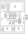
- FIG. 1B a plan view layout of the cascode circuit in an MMIC structure is shown.
- the source (S) of Q1, the gate GATE 1 of Q1, the floating source/drain (S/D), the gate GATE 2 of Q2 and the drain D of Q2 are all on an active region, where a semiconductor mesa region is formed on the upper surface of the substrate.
- the gate GATE 1 of Q1 controls the flow of carriers passing through the active region between the source/drain (S/D) and the source (S) of FET Q1
- the gate of Q2 (GATE 2) controls the flow of carriers passing through the active region between the drain (D) of FET Q2 and the source/drain (S/D).
- the gate of FET Q1 (GATE 1) is fed by an input microwave transmission line, where, for example, a coplanar waveguide (CPW) transmission line having a center conductor disposed between a pair of ground plane conductors is disposed on an upper surface of a substrate.
- the center conductor is connected to a gate pad (GATE PAD 1) for GATE 1 of FET Q1. It is noted that the gate pad (GATE PAD 1) is off of (laterally displaced from) the active region.
- the gate GATE 2 of FET Q2 is connected to a gate pad (GATE PAD 2).
- both GATE PAD 1 and GATE PAD 2 are on the same side of the active region (here, in this layout, both GATE 1 and GATE 2 are on the left side of the active region).
- the drain (D) of the FET Q2 is connected to an output microwave transmission line, here also a CPW transmission line having a center conductor disposed between a pair of ground plane conductors. More particularly, the drain (D) is connected to the center conductor of the output CPW transmission line.
- the gate GATE 2 of FET Q2 is connected to a capacitor disposed on the upper surface of the substrate through the gate pad (GATE PAD 2), and air bridge conductor disposed over the GATE PAD 1 onto the upper plate of the capacitor.
- the lower plate of the capacitor is separated from the upper plate by a dielectric.
- the bottom plate is connected to a ground plane conductor of the output CPW transmission line. It is noted that the ground plane conductor of the input CPW and the output CPW may be connected to a ground plane (not shown) on the bottom surface of the substrate with conductive vias, not shown, passing vertically through the substrate.
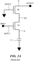
- FIG. 2A Another cascode connected transistor circuit is shown in FIG. 2A and a plan view layout of the cascode circuit in an MMIC structure of FIG. 2A is shown in FIG. 2B .
- the GATE PAD 2 is connected directly to ground and the source (S) is connected to ground through a capacitor.
- the inventors have recognized that a long electrical path exits between the GATE 2 of FET Q2 and ground in both the layout of FIG. 1B and 2B thereby increasing parasitic resistance and inductance on the gate's path to ground decreasing the circuits stability factor and thus effectively lowering Maximum Stable Gain (MSG).
- the inventors have recognized that this long electrical path exists because both gate pads (GATE PAD 1 and GATE PAD 2) are on the same side of the active region and thus a relatively long air bridge is required to "jump-over" or bridge the first gate pad (GATE PAD 1). This effect is particularly important in small, on the order of 50-nm gate length G-band FETs with both gates having the same lengths and a mesa 20um in width.
- a cascode transistor circuit having an active region, the active region having a source, a drain, a floating source/drain, a first gate disposed between the source and the floating source/drain and a second gate disposed between the floating source/drain and the drain.
- a first gate pad is displaced from the active region and is electrically connected to the first gate and a second gate pad is displaced from the active region and is electrically connected to the second gate.
- the first and the second gate pads are on opposite sides of the active region.
- a cascode transistor circuit having: an input transmission line having a conductor disposed on an upper surface of a substrate; an output transmission line having a conductor disposed on the upper surface of the substrate; a first transistor having a gate electrode disposed on the upper surface of the substrate and connected to the conductor of the input transmission line, for controlling a flow of carriers, in a first portion of an active region of the substrate, between a source region of the substrate and a floating source/drain region of the substrate; a second transistor having a gate electrode disposed on the upper surface of the substrate for controlling a flow of carriers in an active region of the substrate between the floating source/drain region of the substrate and a drain region of the substrate, the drain region being connected to the conductor of the output transmission line; a first gate contact pad, laterally displaced from the active region, and connected to one end of the gate electrode of the first transistor; a second gate contact pad, laterally displaced from the active region, and connected to one end of the gate electrode of the second transistor.
- the first gate pad and the second gate pad are disposed on opposite sides of the active region.
- a capacitor is provided having: a lower plate disposed on the upper surface of the substrate; a dielectric disposed on the lower plate; and an upper plate disposed on the dielectric.
- One of the upper and lower plates is connected to either the source or second gate pad and the other one of the upper plate and lower plates is connected to the ground plane conductor portions of at least one of the input transmission line or the output transmission line.
- the lower plate is connected to either the source or second gate pad and the upper plate is connected is connected to the ground plane conductor portions of at least one of the input transmission line or the output transmission line.
- a cascode transistor circuit arrangement having: a pair of laterally spaced cascode transistor circuits, each one having a corresponding one of a pair of active regions, each one of the pair of active regions being disposed on different portion of a surface of a substrate, each one of the active regions having a source, a drain, a floating source/drain, a first gate disposed between the source and the floating source/drain and a second gate disposed between the floating source/drain and the drain; a common gate pad connected to the first gate of both the cascode transistor circuits and displaced from the active region and between the pair of laterally spaced active regions; a first, second gate pad displaced from a first one of the active regions and electrically connected to the second gate of a first one of the pair of cascode connected transistors; a second, second gate pad displaced from a second one of the active regions and electrically connected to the second gate of a second one of the pair of cascode connected transistors.
- the common gate pad and the first, second gate pad is
- a common drain pad is connected to the drain of each one of the pair of cascode transistor circuits.
- the inventors have recognized that placing the gate pads on opposite sides of the active region simplifies the interconnect complexity. Further such an arrangement allows for parallel cascode devices to share a gate (RF input gate) connection and common drain (RF output) connection.
- the common connected gate (the ac grounded gate in the cascode) directly connects to the bottom plate of a capacitor that acts as AC ground. This is a major reduction in series inductance to ground versus the previous state-of-the-art which used a long air-bridge connection. A reduction in inductance to ground should increase maximum available gain of the dual gate at the desired frequency and contribute to greater device stability.
- a cascode transistor circuit 10 having an active region 12, the active region 12 having a source (S), a drain (D), a floating source/drain (S/D), a first gate (G1) disposed between the source (S) and the floating source/drain (S/D) and a second gate (G2) disposed between the floating source drain (S/D) and the drain (D).
- a first gate pad (GP1) is displaced from the active region 12 and is electrically connected to the first gate (G1) and a second gate pad (GP2) is displaced from the active region 12 and is electrically connected to the second gate (G2).
- the first pad (GP1) and the second gate pad (GP2) are disposed on opposite sides of the active region 12, as shown.
- the circuit has a 50-nm gate length (the distance along a direction from the source to the drain) for G-band operation with both gates (G1) and (G2) having the same lengths and wherein the active region 12 is a mesa having a width (a distance along a direction perpendicular to the gate length) of 20um.
- the cascode transistor circuit 10 includes a substrate 14; an input transmission line 16 having a conductor 18 disposed on an upper surface of the substrate 14; an output transmission line 20 having a conductor 22 disposed on the upper surface of the substrate 14; a first transistor Q1 having the gate electrode (G1) disposed on the upper surface of the active region 12 and connected to the conductor 18 of the input transmission line 16, for controlling a flow of carriers, in a first portion of an active region 12 between a source region (S) of the active region 12 and a floating source/drain region (S/D) of the active region 12; a second transistor Q2 having the gate electrode (G2) disposed on the upper surface of the active region 12 for controlling a flow of carriers in the active region 12 between the floating source/drain region (S/D) of the active region 12 and a drain region (D) of the active region 12, the drain region (D) being connected to the conductor 22 of the output transmission line 20; the first gate contact pad (GP1), laterally displaced from the active region 12 (off of
- the first gate pad (GP1) and the second gate pad (GP2) are disposed on opposite sides of the active region mesa 12; here the first gate pad GP1 being shown in FIG. 3 below the mesa active region 12 and the second gate pad (GP2) being on the top side of the active region mesa 12.
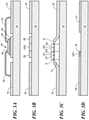
- a capacitor 24 is included having: a lower plate 26 disposed on the upper surface of the substrate 14; a dielectric 28 disposed on the lower plate 26; and an upper plate 30 disposed on the dielectric 28, as shown more clearly in FIG. 3A .
- the mesa or active region 12 is a III-V semiconductor, such as, Gallium Nitride (GaN).
- the input transmission line 16 in this example, is a coplanar waveguide (CPW) transmission line having a center conductor, here conductor 18 disposed between a pair of ground plane conductor portions 19, 21 disposed on the upper surface of the substrate 14.
- the output transmission line, 20, in this example, is also a coplanar waveguide (CPW) transmission line having a center conductor, here conductor 22, disposed between a pair of ground plane conductor portions 21, 23, as shown, output CPW transmission line 20 being disposed on the upper surface of the substrate 14, as shown.
- CPW coplanar waveguide
- the first transistor Q1 has the gate electrode (G1) thereof connected to the center conductor 18 of the input CPW transmission line 16 through the first gate pad (GP1) and the second transistor Q2 has the drain electrode (D) thereof connected to the center conductor 22 of the output CPW transmission line 20 through the drain pad (D), as shown.
- the second gate pad (GP2) is connected to the bottom plate 26 of the capacitor 24 and the top plate 30 of the capacitor 24 is connected to the ground plates 19 and 23 with air-bridges 34, 32, as shown.
- the gate electrode (G1) of the first transistor (Q1) extends laterally from the first gate contact pad (GP1) over the active region 12 along a first direction (in FIG.
- the gate electrode (G2) of the second transistor (Q2) extends laterally from the second gate contact pad (GP2) over the active region 12 parallel to the first direction;
- FIGS. 4 and 5 a schematic diagram of a pair of cascode circuits 10a, 10b and an MMIC plan view layout of the circuit arrangement are shown, respectively.
- the cascode transistor circuit arrangement is shown having: a pair of laterally spaced cascode transistor circuits 10a, 10b ( FIG. 5 ), each circuit 10a, 10b having a pair of transistors Q1a, Q2a, and Qlb, Q2b, respectively as indicated in FIG. 4 , each one of the circuits 10a, 10b having a corresponding one of a pair of active regions 12a, 12b ( FIG. 5 ), each one of the pair of active regions 12a, 12b, being disposed on different portion of a surface of a substrate 14 as shown in FIG.
- Each one of the active regions 12a, 12b has a source (S1a for Q1a and S1b for Q1b), a drain (D1a for Q2a and D1b for Q2b), a floating source/drain (S/D), a first gate (G1a for Q1a and G1b for Q1b) disposed between the source (Sla of Q1a and S1b for Q1b) and the floating source/drain (S/D) and a second gate (G2a for Q2a and G2b for Q2b) disposed between the floating source/drain (S/D) and the drain (D1a for Q2a and D1b for Q2b); a common gate pad (CGP) connected to the first gates (G1a and G1b) of both the cascode transistor circuits 10a, 10b and displaced from the active regions 12a, 12b and between the pair of laterally spaced active regions 12a, 12b; a first, second gate pad (GP2a)
- the common gate pad (CGP) and the first, second gate pad (GP2a) are on opposite sides of the first one of the active regions 12a and the common gate pad (CGP) and the second, second gate pad (GP2b) are on opposite sides of the second one of the active regions 12b.
- a common drain pad (CDP) connected to the drains (D1a, D1b) of each one of the pair of cascode connected transistors Q2a, Q2b in circuits 10a, 10b.
- a pair of capacitors 24a, 24b is provided; a bottom plate of capacitor 24a is connected to the first, second gate (GP2a) of gate (G2a) the transistor circuit 10a and the bottom plate of capacitor 24b is connected to the second, second gate pad (GP2b) for the gate (G2b) of transistor circuit 10b.
- the top plate of capacitor 24a is connected to ground plane conductors 19a and 23a of the input and output CPW transmission lines 16, 20 by air bridges AB1, and AB2 and the top plate of capacitor 24b is connected to ground plane conductors 19b, 23b of the input and output CPW transmission lines 16, 20 by air bridges AB3 and AB4. It is noted that the ground plane 21 ( FIG. 3 ) is separated into two portions 19a and 23a.
- FIG. 2B is a plan view of a top view Monolithic Microwave Integrated Circuit (MMIC) layout of a cascode transistor circuit of FIG. 2A according to the PRIOR ART
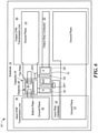
- FIG. 6 is a plan view of a top view Monolithic Microwave Integrated Circuit (MMIC) 10'layout of a cascode transistor circuit of FIG. 2A according to the disclosure.
- MMIC Monolithic Microwave Integrated Circuit
- a cascode transistor circuit may include: an active region having a source, a drain, a floating source/drain; a first gate disposed between the drain and the floating source/drain; a second gate disposed between the floating source drain and the drain; a first gate pad displaced from the active region and electrically connected to the first gate; a second gate pad displaced from the active region and electrically connected to the second gate; and wherein the first and the second gate pads are disposed on opposite sides of the active region.
- the cascode transistor may also include the feature of including a capacitor connected between one of the source or the second gate pad and ground.
- a cascode transistor circuit may include: a substrate; an input transmission line having a conductor disposed on an upper surface of the substrate; an output transmission line having a conductor disposed on the upper surface of the substrate; a first transistor having a gate electrode disposed on the upper surface of the substrate and connected to the conductor of the input transmission line, for controlling a flow of carriers, in a first portion of an active region of the substrate, between a source region of the substrate and a floating source/drain region of the substrate; a second transistor having a gate electrode disposed on the upper surface of the substrate for controlling a flow of carriers in an active region of the substrate between the floating source/drain region of the substrate and a drain region of the substrate, the drain region being connected to the conductor of the output transmission line; a first gate contact pad, laterally displaced from the active region, and connected to one end of the gate electrode of the first transistor; a second gate contact pad, laterally displaced from the active region, and connected to one end of the gate electrode
- a cascode transistor circuit may include: a substrate; an input coplanar waveguide (CPW) transmission line having a center conductor disposed between a pair of ground plane conductor portions, the input CPW transmission line being disposed on a surface of the substrate; an output coplanar waveguide (CPW) transmission line having a center conductor disposed between a pair of ground plane conductor portions, the output CPW transmission line being disposed on the surface of the substrate; a first transistor having a gate electrode disposed on the surface of the substrate and connected to the center conductor of the input CPW transmission line, for controlling a flow of carriers, in a first portion of an active region of the substrate, between a source region of the substrate and a floating source/drain region of the substrate; a second transistor having a gate electrode disposed on a surface of the substrate for controlling a flow of carriers in an active region of the substrate between the floating source/drain region of the substrate and a drain region of the substrate, the drain region being connected to
- the cascode transistor circuit may also include the features wherein the gate electrode of the first transistor extending laterally from the first gate contact pad over the active region portion along a first direction; the gate electrode of the second transistor extending laterally from the second gate contact pad over the active region portion parallel to the first direction; including a conductor for connecting the upper plate to the ground plane conductor portions of at least one of the input CPW transmission line or the output CPW transmission line, the conductor extending along a direction perpendicular to the first direction. Still further, the cascode transistor circuit may also include the feature wherein the conductor is an air-bridge conductor.
- a cascode transistor circuit arrangement may include: a pair of laterally spaced cascode transistor circuits, each one having a corresponding one of a pair of active regions, each one of the pair of active regions being disposed on different portion of a surface of a substrate, each one of the active regions having a source, a drain, a floating source/drain, a first gate disposed between the source and the floating source/drain and a second gate disposed between the floating source drain and the drain; a common gate pad connected to the first gate of both the cascode transistor circuits and displaced from the active region and between the pair of laterally spaced active regions; a first, second gate pad displaced from a first one of the active regions and electrically connected to the second gate of a first one of the pair of cascode connected transforms; a second, second gate pad displaced from a second one of the active regions and electrically connected to the second gate of a second one of the pair of cascode connected transistors; wherein the common gate pad and the
- the dielectric of the capacitor may extend over the bottom conductor eliminating the need for an air bridge type conductor.
- other transmission lines than CPW may be used such as microstrip transmission line wherein the ground plane is on the bottom surface of the substrate.
- a ground plane may be formed on the bottom surface of the substrate and may be connected to the CPW transmission line ground planes with conductive vias passing vertically though the substrate.
- semiconductor materials may be used in place of GaN.
- the active region need not be a mesa but merely a semiconductor region wherein carriers pass and are controlled by the gate. Accordingly, other embodiments are within the scope of the following claims.
- a cascode transistor circuit comprising:
- Embodiment 2 The cascode transistor circuit recited in embodiment 1 including a capacitor connected between one of the source or the second gate pad and ground.
- a cascode transistor circuit comprising:
- Embodiment 4 The cascode transistor circuit recited in embodiment 3 wherein the lower plate is connected to one of the source or the second gate pad and the upper plate is connected to the ground plane conductor portions of at least one of the input transmission line or the output transmission line.
- a cascode transistor circuit comprising:
- Embodiment 6 The cascode transistor circuit recited in embodiment 5 wherein:
- Embodiment 7 The cascode transistor circuit recited in embodiment 6 wherein the conductor is an air-bridge conductor.
- Embodiment 8 A cascode transistor circuit arrangement, comprising:
- Embodiment 9 The cascode transistor circuit arrangement recited in embodiment 8 including a common drain pad connected to the drain of each one of the pair of cascode transistor circuits.
Landscapes
- Engineering & Computer Science (AREA)
- Power Engineering (AREA)
- Microelectronics & Electronic Packaging (AREA)
- Junction Field-Effect Transistors (AREA)
Abstract
Description
- This disclosure relates generally to microwave monolithic integrated circuits (MMICs) and more particularly to MMICs having cascode connected transistors.
- As is known in the art, cascode connected transistor circuit (
FIG. 1A ) includes a pair of transistors Q1, Q2 arranged as a two-stage amplifier; a common-source transconductance amplifier section formed by one of the transistors Q1 and followed by a common-gate current buffer amplifier section formed by the one of the second transistors Q2. Thus, the cascode is a dual gate device or circuit. A schematic diagram of one such arrangement is shown inFIG. 1A . Here, the transistors Q1, Q2 are Field Effect Transistors (FETs). It is noted that the transconductance amplifier section includes a common (grounded) source (S) FET Q1 having its gate electrode (GATE1) fed by an input signal. The current buffer amplifier section includes a common (grounded) gate (GATE2) FET Q2 having its gate connected to ground through a capacitor (C). The source (S) of the common (grounded) gate (S) FET Q2 and the drain (D) of the common source FET Q1 are connected together to provide a floating source/drain (S/D), as indicated. The amplified input signal is produced as an output signal at the drain (D) of FET Q2. - It is noted it that, in referring to
FIG. 1B , a plan view layout of the cascode circuit in an MMIC structure is shown. It is first noted that the source (S) of Q1, thegate GATE 1 of Q1, the floating source/drain (S/D), thegate GATE 2 of Q2 and the drain D of Q2 are all on an active region, where a semiconductor mesa region is formed on the upper surface of the substrate. Thus, thegate GATE 1 of Q1 controls the flow of carriers passing through the active region between the source/drain (S/D) and the source (S) of FET Q1 and the gate of Q2 (GATE 2) controls the flow of carriers passing through the active region between the drain (D) of FET Q2 and the source/drain (S/D). The gate of FET Q1 (GATE 1) is fed by an input microwave transmission line, where, for example, a coplanar waveguide (CPW) transmission line having a center conductor disposed between a pair of ground plane conductors is disposed on an upper surface of a substrate. The center conductor is connected to a gate pad (GATE PAD 1) forGATE 1 of FET Q1. It is noted that the gate pad (GATE PAD 1) is off of (laterally displaced from) the active region. Thegate GATE 2 of FET Q2 is connected to a gate pad (GATE PAD 2). It is noted is also noted that: (1) the gate pad (GATE PAD 2) is also off of (laterally displaced from) the active region and (2) bothGATE PAD 1 andGATE PAD 2 are on the same side of the active region (here, in this layout, bothGATE 1 andGATE 2 are on the left side of the active region). The drain (D) of the FET Q2 is connected to an output microwave transmission line, here also a CPW transmission line having a center conductor disposed between a pair of ground plane conductors. More particularly, the drain (D) is connected to the center conductor of the output CPW transmission line. Thegate GATE 2 of FET Q2 is connected to a capacitor disposed on the upper surface of the substrate through the gate pad (GATE PAD 2), and air bridge conductor disposed over theGATE PAD 1 onto the upper plate of the capacitor. The lower plate of the capacitor is separated from the upper plate by a dielectric. The bottom plate is connected to a ground plane conductor of the output CPW transmission line. It is noted that the ground plane conductor of the input CPW and the output CPW may be connected to a ground plane (not shown) on the bottom surface of the substrate with conductive vias, not shown, passing vertically through the substrate. - Another cascode connected transistor circuit is shown in
FIG. 2A and a plan view layout of the cascode circuit in an MMIC structure ofFIG. 2A is shown inFIG. 2B . Here, the GATE PAD 2 is connected directly to ground and the source (S) is connected to ground through a capacitor. - The inventors have recognized that a long electrical path exits between the
GATE 2 of FET Q2 and ground in both the layout ofFIG. 1B and2B thereby increasing parasitic resistance and inductance on the gate's path to ground decreasing the circuits stability factor and thus effectively lowering Maximum Stable Gain (MSG). The inventors have recognized that this long electrical path exists because both gate pads (GATE PAD 1 and GATE PAD 2) are on the same side of the active region and thus a relatively long air bridge is required to "jump-over" or bridge the first gate pad (GATE PAD 1). This effect is particularly important in small, on the order of 50-nm gate length G-band FETs with both gates having the same lengths and a mesa 20um in width. - In accordance with the present disclosure, a cascode transistor circuit is provided having an active region, the active region having a source, a drain, a floating source/drain, a first gate disposed between the source and the floating source/drain and a second gate disposed between the floating source/drain and the drain. A first gate pad is displaced from the active region and is electrically connected to the first gate and a second gate pad is displaced from the active region and is electrically connected to the second gate. The first and the second gate pads are on opposite sides of the active region.
- In one embodiment, a cascode transistor circuit is provided having: an input transmission line having a conductor disposed on an upper surface of a substrate; an output transmission line having a conductor disposed on the upper surface of the substrate; a first transistor having a gate electrode disposed on the upper surface of the substrate and connected to the conductor of the input transmission line, for controlling a flow of carriers, in a first portion of an active region of the substrate, between a source region of the substrate and a floating source/drain region of the substrate; a second transistor having a gate electrode disposed on the upper surface of the substrate for controlling a flow of carriers in an active region of the substrate between the floating source/drain region of the substrate and a drain region of the substrate, the drain region being connected to the conductor of the output transmission line; a first gate contact pad, laterally displaced from the active region, and connected to one end of the gate electrode of the first transistor; a second gate contact pad, laterally displaced from the active region, and connected to one end of the gate electrode of the second transistor. The first gate pad and the second gate pad are disposed on opposite sides of the active region. A capacitor is provided having: a lower plate disposed on the upper surface of the substrate; a dielectric disposed on the lower plate; and an upper plate disposed on the dielectric. One of the upper and lower plates is connected to either the source or second gate pad and the other one of the upper plate and lower plates is connected to the ground plane conductor portions of at least one of the input transmission line or the output transmission line.
- In one embodiment, the lower plate is connected to either the source or second gate pad and the upper plate is connected is connected to the ground plane conductor portions of at least one of the input transmission line or the output transmission line.
- In one embodiment, a cascode transistor circuit arrangement is provided having: a pair of laterally spaced cascode transistor circuits, each one having a corresponding one of a pair of active regions, each one of the pair of active regions being disposed on different portion of a surface of a substrate, each one of the active regions having a source, a drain, a floating source/drain, a first gate disposed between the source and the floating source/drain and a second gate disposed between the floating source/drain and the drain; a common gate pad connected to the first gate of both the cascode transistor circuits and displaced from the active region and between the pair of laterally spaced active regions; a first, second gate pad displaced from a first one of the active regions and electrically connected to the second gate of a first one of the pair of cascode connected transistors; a second, second gate pad displaced from a second one of the active regions and electrically connected to the second gate of a second one of the pair of cascode connected transistors. The common gate pad and the first, second gate pad are on opposite sides of the first one of the active regions and the common gate pad and the second, second gate pad are on opposite sides of the second one of the active regions.
- In one embodiment, a common drain pad is connected to the drain of each one of the pair of cascode transistor circuits.
- Thus the inventors have recognized that placing the gate pads on opposite sides of the active region simplifies the interconnect complexity. Further such an arrangement allows for parallel cascode devices to share a gate (RF input gate) connection and common drain (RF output) connection. The common connected gate (the ac grounded gate in the cascode) directly connects to the bottom plate of a capacitor that acts as AC ground. This is a major reduction in series inductance to ground versus the previous state-of-the-art which used a long air-bridge connection. A reduction in inductance to ground should increase maximum available gain of the dual gate at the desired frequency and contribute to greater device stability.
- The details of one or more embodiments of the disclosure are set forth in the accompanying drawings and the description below. Other features, objects, and advantages of the disclosure will be apparent from the description and drawings, and from the claims.
-
-
FIGS. 1A and1B are a schematic diagram of a cascode transistor circuit and a plan view Monolithic Microwave Integrated Circuit (MMIC) layout of the cascode transistor circuit ofFIG. 1A , respectively, according to the PRIOR ART; -
FIGS. 2A and2B area schematic diagram of another cascode transistor circuit and is a plan view of a top view Monolithic Microwave Integrated Circuit (MMIC) layout of the cascode transistor circuit ofFIG. 2A , respectively, according to the PRIOR ART; -
FIG. 3 is a plan view of a top view Monolithic Microwave Integrated Circuit (MMIC) layout of the cascode transistor circuit ofFIG. 1 according to the disclosure; -
FIGS. 3A through 3D are cross sectional views of the Monolithic Microwave Integrated Circuit (MMIC) layout of the cascode transistor circuit ofFIG. 3 taken alonglines 3A-3A through 3D-3D, respectively; -
FIG. 4 is a is a schematic diagram of a pair of cascode transistor circuits according to the PRIOR ART; -
FIG. 5 is a plan view of a top view Monolithic Microwave Integrated Circuit (MMIC) layout of a pair of cascode transistor circuits ofFIG. 4 according to another embodiment of the disclosure; and -
FIG. 6 is a plan view of a top view Monolithic Microwave Integrated Circuit (MMIC) layout of a cascode transistor circuit ofFIG. 2A according to still another embodiment of the disclosure. - Like reference symbols in the various drawings indicate like elements.
- Referring now to
FIG. 3 , acascode transistor circuit 10 is shown having anactive region 12, theactive region 12 having a source (S), a drain (D), a floating source/drain (S/D), a first gate (G1) disposed between the source (S) and the floating source/drain (S/D) and a second gate (G2) disposed between the floating source drain (S/D) and the drain (D). A first gate pad (GP1) is displaced from theactive region 12 and is electrically connected to the first gate (G1) and a second gate pad (GP2) is displaced from theactive region 12 and is electrically connected to the second gate (G2). The first pad (GP1) and the second gate pad (GP2) are disposed on opposite sides of theactive region 12, as shown. Here, in this example, the circuit has a 50-nm gate length (the distance along a direction from the source to the drain) for G-band operation with both gates (G1) and (G2) having the same lengths and wherein theactive region 12 is a mesa having a width (a distance along a direction perpendicular to the gate length) of 20um. - More particularly, the cascode transistor circuit 10 includes a substrate 14; an input transmission line 16 having a conductor 18 disposed on an upper surface of the substrate 14; an output transmission line 20 having a conductor 22 disposed on the upper surface of the substrate 14; a first transistor Q1 having the gate electrode (G1) disposed on the upper surface of the active region 12 and connected to the conductor 18 of the input transmission line 16, for controlling a flow of carriers, in a first portion of an active region 12 between a source region (S) of the active region 12 and a floating source/drain region (S/D) of the active region 12; a second transistor Q2 having the gate electrode (G2) disposed on the upper surface of the active region 12 for controlling a flow of carriers in the active region 12 between the floating source/drain region (S/D) of the active region 12 and a drain region (D) of the active region 12, the drain region (D) being connected to the conductor 22 of the output transmission line 20; the first gate contact pad (GP1), laterally displaced from the active region 12 (off of the mesa), and connected to one end of the gate electrode (G1) of the first transistor (Q1); the second gate contact pad (GP2), laterally displaced from the active region 12 (off of the mesa), and connected to one end of the gate electrode (G2) of the second transistor (Q2). As noted above, the first gate pad (GP1) and the second gate pad (GP2) are disposed on opposite sides of the
active region mesa 12; here the first gate pad GP1 being shown inFIG. 3 below the mesaactive region 12 and the second gate pad (GP2) being on the top side of theactive region mesa 12. Acapacitor 24 is included having: alower plate 26 disposed on the upper surface of thesubstrate 14; a dielectric 28 disposed on thelower plate 26; and anupper plate 30 disposed on the dielectric 28, as shown more clearly inFIG. 3A . Here, for example, the mesa oractive region 12 is a III-V semiconductor, such as, Gallium Nitride (GaN). - More particularly, the
input transmission line 16, in this example, is a coplanar waveguide (CPW) transmission line having a center conductor, hereconductor 18 disposed between a pair of groundplane conductor portions substrate 14. The output transmission line, 20, in this example, is also a coplanar waveguide (CPW) transmission line having a center conductor, hereconductor 22, disposed between a pair of groundplane conductor portions CPW transmission line 20 being disposed on the upper surface of thesubstrate 14, as shown. - It is noted that the first transistor Q1 has the gate electrode (G1) thereof connected to the
center conductor 18 of the inputCPW transmission line 16 through the first gate pad (GP1) and the second transistor Q2 has the drain electrode (D) thereof connected to thecenter conductor 22 of the outputCPW transmission line 20 through the drain pad (D), as shown. - It is also noted that the second gate pad (GP2) is connected to the
bottom plate 26 of thecapacitor 24 and thetop plate 30 of thecapacitor 24 is connected to theground plates bridges active region 12 along a first direction (inFIG. 3 an up-down direction); the gate electrode (G2) of the second transistor (Q2) extends laterally from the second gate contact pad (GP2) over theactive region 12 parallel to the first direction; theconductors upper plate 30 to the groundplane conductor portions CPW transmission line 16 and the outputCPW transmission line 20, respectively, extend along a direction perpendicular to the first direction (the right to left direction inFIG. 3 ). - It is noted that the electrical path between the second gate pad (GP2) and ground in
FIG. 3 is shorter compared with the layout ofFIG. 1B because both gate pads (GATE PAD 1 and GATE PAD 2) are on the opposing sides of the active region and thus the relatively long air bridge ofFIG. 1B is no longer required to "jump-over" or bridge the first gate pad (GATE PAD 1). - Referring now to
FIGS. 4 and5 , a schematic diagram of a pair ofcascode circuits cascode transistor circuits FIG. 5 ), eachcircuit FIG. 4 , each one of thecircuits active regions FIG. 5 ), each one of the pair ofactive regions substrate 14 as shown inFIG. 5 . Each one of the active regions 12a, 12b, has a source (S1a for Q1a and S1b for Q1b), a drain (D1a for Q2a and D1b for Q2b), a floating source/drain (S/D), a first gate (G1a for Q1a and G1b for Q1b) disposed between the source (Sla of Q1a and S1b for Q1b) and the floating source/drain (S/D) and a second gate (G2a for Q2a and G2b for Q2b) disposed between the floating source/drain (S/D) and the drain (D1a for Q2a and D1b for Q2b); a common gate pad (CGP) connected to the first gates (G1a and G1b) of both the cascode transistor circuits 10a, 10b and displaced from the active regions 12a, 12b and between the pair of laterally spaced active regions 12a, 12b; a first, second gate pad (GP2a) displaced from a first one of the active regions 12a and electrically connected to the second gate (G2a) of a first one of the pair of cascode connected transistors Q2a); a second, second gate pad (GP2b) displaced from a second one of the active regions 12b and electrically connected to the second gate (G2b) of a second one of the pair of cascode connected transistors Q2b. The common gate pad (CGP) and the first, second gate pad (GP2a) are on opposite sides of the first one of theactive regions 12a and the common gate pad (CGP) and the second, second gate pad (GP2b) are on opposite sides of the second one of theactive regions 12b. Also included is a common drain pad (CDP) connected to the drains (D1a, D1b) of each one of the pair of cascode connected transistors Q2a, Q2b incircuits - A pair of
capacitors capacitor 24a is connected to the first, second gate (GP2a) of gate (G2a) thetransistor circuit 10a and the bottom plate ofcapacitor 24b is connected to the second, second gate pad (GP2b) for the gate (G2b) oftransistor circuit 10b. The top plate ofcapacitor 24a is connected to groundplane conductors CPW transmission lines capacitor 24b is connected to groundplane conductors CPW transmission lines FIG. 3 ) is separated into twoportions -
FIG. 2B is a plan view of a top view Monolithic Microwave Integrated Circuit (MMIC) layout of a cascode transistor circuit ofFIG. 2A according to the PRIOR ART andFIG. 6 is a plan view of a top view Monolithic Microwave Integrated Circuit (MMIC) 10'layout of a cascode transistor circuit ofFIG. 2A according to the disclosure. Here again it is noted that the electrical path between the second gate pad (GP2) and ground is shorter compared with the layout ofFIG. 2B , because both gate pads (GATE PAD 1 and GATE PAD 2) are on opposing sides of the active region and thus the relatively long air bridge ofFIG. 2B is no longer required to "jump-over" or bridge the first gate pad (GATE PAD 1). - It should now be appreciated a cascode transistor circuit according to the disclosure may include: an active region having a source, a drain, a floating source/drain; a first gate disposed between the drain and the floating source/drain; a second gate disposed between the floating source drain and the drain; a first gate pad displaced from the active region and electrically connected to the first gate; a second gate pad displaced from the active region and electrically connected to the second gate; and wherein the first and the second gate pads are disposed on opposite sides of the active region. The cascode transistor may also include the feature of including a capacitor connected between one of the source or the second gate pad and ground.
- It should now also be appreciated a cascode transistor circuit according to the disclosure may include: a substrate; an input transmission line having a conductor disposed on an upper surface of the substrate; an output transmission line having a conductor disposed on the upper surface of the substrate; a first transistor having a gate electrode disposed on the upper surface of the substrate and connected to the conductor of the input transmission line, for controlling a flow of carriers, in a first portion of an active region of the substrate, between a source region of the substrate and a floating source/drain region of the substrate; a second transistor having a gate electrode disposed on the upper surface of the substrate for controlling a flow of carriers in an active region of the substrate between the floating source/drain region of the substrate and a drain region of the substrate, the drain region being connected to the conductor of the output transmission line; a first gate contact pad, laterally displaced from the active region, and connected to one end of the gate electrode of the first transistor; a second gate contact pad, laterally displaced from the active region, and connected to one end of the gate electrode of the second transistor; and wherein the first gate pad and the second gate pad are disposed on opposite sides of the active region; a capacitor, comprising: a lower plate disposed on the upper surface of the substrate; a dielectric disposed on the lower plate; and an upper plate disposed on the dielectric; and wherein one of the upper and lower plates is connected to one of the source or second gate pad and the other one of the upper plate and lower plates is connected to the ground plane conductor portions of at least one of the input transmission line or the output transmission line. The cascode transistor may also include the feature wherein the lower plate is connected to one of the source or the second gate pad and the upper plate is connected to the ground plane conductor portions of at least one of the input transmission line or the output transmission line.
- It should now also be appreciated a cascode transistor circuit according to the disclosure may include: a substrate; an input coplanar waveguide (CPW) transmission line having a center conductor disposed between a pair of ground plane conductor portions, the input CPW transmission line being disposed on a surface of the substrate; an output coplanar waveguide (CPW) transmission line having a center conductor disposed between a pair of ground plane conductor portions, the output CPW transmission line being disposed on the surface of the substrate; a first transistor having a gate electrode disposed on the surface of the substrate and connected to the center conductor of the input CPW transmission line, for controlling a flow of carriers, in a first portion of an active region of the substrate, between a source region of the substrate and a floating source/drain region of the substrate; a second transistor having a gate electrode disposed on a surface of the substrate for controlling a flow of carriers in an active region of the substrate between the floating source/drain region of the substrate and a drain region of the substrate, the drain region being connected to the center conductor of the output CPW transmission line; a first gate contact pad, laterally displaced from the active region, and connected to one end of the gate electrode of the first transistor; a second gate contact pad, laterally displaced from the active region, and connected to one end of the gate electrode of the second transistor; and wherein the first gate pad and the second gate pad are disposed on opposite sides of the active region; a capacitor comprising: a lower plate disposed on the surface of the substrate; a dielectric disposed on the lower plate; and an upper plate disposed on the dielectric; and wherein the lower plate is connected to one of the source or the second gate pad and the upper plate is connected to the ground plane conductor portions of at least one of the input CPW transmission line or the output CPW transmission line. The cascode transistor circuit may also include the features wherein the gate electrode of the first transistor extending laterally from the first gate contact pad over the active region portion along a first direction; the gate electrode of the second transistor extending laterally from the second gate contact pad over the active region portion parallel to the first direction; including a conductor for connecting the upper plate to the ground plane conductor portions of at least one of the input CPW transmission line or the output CPW transmission line, the conductor extending along a direction perpendicular to the first direction. Still further, the cascode transistor circuit may also include the feature wherein the conductor is an air-bridge conductor.
- It should now also be appreciated a cascode transistor circuit arrangement according to the disclosure may include: a pair of laterally spaced cascode transistor circuits, each one having a corresponding one of a pair of active regions, each one of the pair of active regions being disposed on different portion of a surface of a substrate, each one of the active regions having a source, a drain, a floating source/drain, a first gate disposed between the source and the floating source/drain and a second gate disposed between the floating source drain and the drain; a common gate pad connected to the first gate of both the cascode transistor circuits and displaced from the active region and between the pair of laterally spaced active regions; a first, second gate pad displaced from a first one of the active regions and electrically connected to the second gate of a first one of the pair of cascode connected transforms; a second, second gate pad displaced from a second one of the active regions and electrically connected to the second gate of a second one of the pair of cascode connected transistors; wherein the common gate pad and the first, second gate pad are on opposite sides of the first one of the active regions and the common gate pad and the second, second gate pad are on opposite sides of the second one of the active regions. The cascode transistor circuit arrangement may also include the feature including a common drain pad connected to the drain of each one of the pair of cascode transistor circuits.
- A number of embodiments of the disclosure have been described. Nevertheless, it will be understood that various modifications may be made without departing from the spirit and scope of the disclosure. For example, the dielectric of the capacitor may extend over the bottom conductor eliminating the need for an air bridge type conductor. Also, other transmission lines than CPW may be used such as microstrip transmission line wherein the ground plane is on the bottom surface of the substrate. Further, with the CPW transmission lines, a ground plane may be formed on the bottom surface of the substrate and may be connected to the CPW transmission line ground planes with conductive vias passing vertically though the substrate. Still further other semiconductor materials may be used in place of GaN. Still further, the active region need not be a mesa but merely a semiconductor region wherein carriers pass and are controlled by the gate. Accordingly, other embodiments are within the scope of the following claims.
- The following non-exhaustive list of embodiments also forms part of the present disclosure.
-
Embodiment 1. A cascode transistor circuit, comprising: - an active region having a source, a drain, a floating source/drain;
- a first gate disposed between the drain and the floating source/drain;
- a second gate disposed between the floating source drain and the drain;
- a first gate pad displaced from the active region and electrically connected to the first gate;
- a second gate pad displaced from the active region and electrically connected to the second gate; and
- wherein the first and the second gate pads are disposed on opposite sides of the active region.
-
Embodiment 2. The cascode transistor circuit recited inembodiment 1 including a capacitor connected between one of the source or the second gate pad and ground. - Embodiment 3. A cascode transistor circuit, comprising:
- a substrate;
- an input transmission line having a conductor disposed on an upper surface of the substrate;
- an output transmission line having a conductor disposed on the upper surface of the substrate;
- a first transistor having a gate electrode disposed on the upper surface of the substrate and connected to the conductor of the input transmission line, for controlling a flow of carriers, in a first portion of an active region of the substrate, between a source region of the substrate and a floating source/drain region of the substrate;
- a second transistor having a gate electrode disposed on the upper surface of the substrate for controlling a flow of carriers in an active region of the substrate between the floating source/drain region of the substrate and a drain region of the substrate, the drain region being connected to the conductor of the output transmission line;
- a first gate contact pad, laterally displaced from the active region, and connected to one end of the gate electrode of the first transistor;
- a second gate contact pad, laterally displaced from the active region, and connected to one end of the gate electrode of the second transistor; and
wherein the first gate pad and the second gate pad are disposed on opposite sides of the active region; - a capacitor, comprising:
- a lower plate disposed on the upper surface of the substrate;
- a dielectric disposed on the lower plate; and
- an upper plate disposed on the dielectric; and
- wherein one of the upper and lower plates is connected to one of the source or second gate pad and the other one of the upper plate and lower plates is connected to the ground plane conductor portions of at least one of the input transmission line or the output transmission line.
- Embodiment 4. The cascode transistor circuit recited in embodiment 3 wherein the lower plate is connected to one of the source or the second gate pad and the upper plate is connected to the ground plane conductor portions of at least one of the input transmission line or the output transmission line.
- Embodiment 5. A cascode transistor circuit, comprising:
- a substrate;
- an input coplanar waveguide (CPW) transmission line having a center conductor disposed between a pair of ground plane conductor portions, the input CPW transmission line being disposed on a surface of the substrate;
- an output coplanar waveguide (CPW) transmission line having a center conductor disposed between a pair of ground plane conductor portions, the output CPW transmission line being disposed on the surface of the substrate;
- a first transistor having a gate electrode disposed on the surface of the substrate and connected to the center conductor of the input CPW transmission line, for controlling a flow of carriers, in a first portion of an active region of the substrate, between a source region of the substrate and a floating source/drain region of the substrate;
- a second transistor having a gate electrode disposed on a surface of the substrate for controlling a flow of carriers in an active region of the substrate between the floating source/drain region of the substrate and a drain region of the substrate, the drain region being connected to the center conductor of the output CPW transmission line;
- a first gate contact pad, laterally displaced from the active region, and connected to one end of the gate electrode of the first transistor;
- a second gate contact pad, laterally displaced from the active region, and connected to one end of the gate electrode of the second transistor; and
wherein the first gate pad and the second gate pad are disposed on opposite sides of the active region; - a capacitor comprising:
- a lower plate disposed on the surface of the substrate;
- a dielectric disposed on the lower plate; and
- an upper plate disposed on the dielectric; and
- wherein the lower plate is connected to one of the source or the second gate pad and the upper plate is connected to the ground plane conductor portions of at least one of the input CPW transmission line or the output CPW transmission line.
- Embodiment 6. The cascode transistor circuit recited in embodiment 5 wherein:
- the gate electrode of the first transistor extending laterally from the first gate contact pad over the active region portion along a first direction;
- the gate electrode of the second transistor extending laterally from the second gate contact pad over the active region portion parallel to the first direction;
- including a conductor for connecting the upper plate to the ground plane conductor portions of at least one of the input CPW transmission line or the output CPW transmission line, the conductor extending along a direction perpendicular to the first direction.
- Embodiment 7. The cascode transistor circuit recited in embodiment 6 wherein the conductor is an air-bridge conductor.
-
Embodiment 8. A cascode transistor circuit arrangement, comprising: - a pair of laterally spaced cascode transistor circuits, each one having a corresponding one of a pair of active regions, each one of the pair of active regions being disposed on different portion of a surface of a substrate, each one of the active regions having a source, a drain, a floating source/drain, a first gate disposed between the source and the floating source/drain and a second gate disposed between the floating source drain and the drain;
- a common gate pad connected to the first gate of both the cascode transistor circuits and displaced from the active region and between the pair of laterally spaced active regions;
- a first, second gate pad displaced from a first one of the active regions and electrically connected to the second gate of a first one of the pair of cascode connected transforms;
- a second, second gate pad displaced from a second one of the active regions and electrically connected to the second gate of a second one of the pair of cascode connected transistors;
- wherein the common gate pad and the first, second gate pad are on opposite sides of the first one of the active regions and the common gate pad and the second, second gate pad are on opposite sides of the second one of the active regions.
- Embodiment 9. The cascode transistor circuit arrangement recited in
embodiment 8 including a common drain pad connected to the drain of each one of the pair of cascode transistor circuits.
Claims (12)
- A cascode transistor circuit, comprising:an active region having a source, a drain, a floating source/drain;a first gate disposed between the drain and the floating source/drain;a second gate disposed between the floating source drain and the drain;a first gate pad displaced from the active region and electrically connected to the first gate;a second gate pad displaced from the active region and electrically connected to the second gate; andwherein the first and the second gate pads are disposed on opposite sides of the active region.
- The cascode transistor circuit recited in claim 1 including a capacitor connected between one of the source or the second gate pad and ground.
- The cascode transistor circuit recited in claim 1, comprising:a substrate;an input transmission line having a conductor disposed on an upper surface of the substrate;an output transmission line having a conductor disposed on the upper surface of the substrate;a first transistor having the first gate comprising a gate electrode disposed on the upper surface of the substrate and connected to the conductor of the input transmission line, for controlling a flow of carriers, in a first portion of the active region of the substrate, between the source comprising a source region of the substrate and the floating source/drain comprising a floating source/drain region of the substrate;a second transistor having the second gate comprising a gate electrode disposed on the upper surface of the substrate for controlling a flow of carriers in the active region of the substrate between the floating source/drain region of the substrate and the drain comprising a drain region of the substrate, the drain region being connected to the conductor of the output transmission line;the first gate pad comprising a first gate contact pad, laterally displaced from the active region, and connected to one end of the gate electrode of the first transistor;the second gate pad comprising a second gate contact pad, laterally displaced from the active region, and connected to one end of the gate electrode of the second transistor; and
wherein the first gate pad and the second gate pad are disposed on opposite sides of the active region;a capacitor, comprising:a lower plate disposed on the upper surface of the substrate;a dielectric disposed on the lower plate; andan upper plate disposed on the dielectric; andwherein one of the upper and lower plates is connected to one of the source or second gate pad and the other one of the upper plate and lower plates is connected to the ground plane conductor portions of at least one of the input transmission line or the output transmission line. - The cascode transistor circuit recited in claim 3 wherein the lower plate is connected to one of the source or the second gate pad and the upper plate is connected to the ground plane conductor portions of at least one of the input transmission line or the output transmission line.
- The cascode transistor circuit recited in claim 1, comprising:a substrate;an input coplanar waveguide (CPW) transmission line having a center conductor disposed between a pair of ground plane conductor portions, the input CPW transmission line being disposed on a surface of the substrate;an output coplanar waveguide (CPW) transmission line having a center conductor disposed between a pair of ground plane conductor portions, the output CPW transmission line being disposed on the surface of the substrate;a first transistor having the first gate comprising a gate electrode disposed on the surface of the substrate and connected to the center conductor of the input CPW transmission line, for controlling a flow of carriers, in a first portion of the active region of the substrate, between the source comprising a source region of the substrate and the floating source/drain comprising a floating source/drain region of the substrate;a second transistor having the second gate comprising a gate electrode disposed on a surface of the substrate for controlling a flow of carriers in the active region of the substrate between the floating source/drain region of the substrate and the drain comprising a drain region of the substrate, the drain region being connected to the center conductor of the output CPW transmission line;the first gate pad comprising a first gate contact pad, laterally displaced from the active region, and connected to one end of the gate electrode of the first transistor;the second gate pad comprising a second gate contact pad, laterally displaced from the active region, and connected to one end of the gate electrode of the second transistor; and
wherein the first gate pad and the second gate pad are disposed on opposite sides of the active region;a capacitor comprising:a lower plate disposed on the surface of the substrate;a dielectric disposed on the lower plate; andan upper plate disposed on the dielectric; andwherein the lower plate is connected to one of the source or the second gate pad and the upper plate is connected to the ground plane conductor portions of at least one of the input CPW transmission line or the output CPW transmission line. - The cascode transistor circuit recited in claim 5, wherein the lower plate is connected to the second gate pad, and wherein the upper plate is connected to the ground plane conductor portion of the input CPW transmission line and the ground plane conductor portion of the output transmission line via air-bridges.
- The cascode transistor circuit recited in claim 5 wherein:the gate electrode of the first transistor extending laterally from the first gate contact pad over the active region portion along a first direction;the gate electrode of the second transistor extending laterally from the second gate contact pad over the active region portion parallel to the first direction;including a conductor for connecting the upper plate to the ground plane conductor portions of at least one of the input CPW transmission line or the output CPW transmission line, the conductor extending along a direction perpendicular to the first direction.
- The cascode transistor circuit recited in claim 7 wherein the conductor is an air-bridge conductor.
- The cascode transistor circuit of any preceding claim, wherein the first gate and second gate have a 50-nm gate length.
- The cascode transistor circuit of any preceding claim, wherein the active region is a mesa having a width of 20um.
- A cascode transistor circuit arrangement, comprising:a pair of cascode transistor circuits comprising a first cascode transistor circuit of claim 1 laterally spaced from a second cascode transistor circuit of claim 1,
wherein each one of the active regions of the pair of cascode transistor circuits is disposed on a different portion of a surface of a substrate,wherein the first gate pad of each one of the cascode transistor circuits comprises a common gate pad connected to the first gate of both of the cascode transistor circuits, wherein the common gate pad is displaced from the laterally spaced active regions and is between the pair of laterally spaced active regions. - The cascode transistor circuit arrangement recited in claim 11 including a common drain pad connected to the drain of each one of the pair of cascode transistor circuits.
Applications Claiming Priority (3)
| Application Number | Priority Date | Filing Date | Title |
|---|---|---|---|
| US14/663,974 US9613947B2 (en) | 2015-03-20 | 2015-03-20 | Monolithic microwave integrated circuit (MMIC) cascode connected transistor circuit |
| EP16716974.7A EP3272006A1 (en) | 2015-03-20 | 2016-03-18 | Monolithic microwave integrated circuit (mmic) cascode connected transistor circuit |
| PCT/US2016/023045 WO2016153970A1 (en) | 2015-03-20 | 2016-03-18 | Monolithic microwave integrated circuit (mmic) cascode connected transistor circuit |
Related Parent Applications (1)
| Application Number | Title | Priority Date | Filing Date |
|---|---|---|---|
| EP16716974.7A Division EP3272006A1 (en) | 2015-03-20 | 2016-03-18 | Monolithic microwave integrated circuit (mmic) cascode connected transistor circuit |
Publications (1)
| Publication Number | Publication Date |
|---|---|
| EP3952108A1 true EP3952108A1 (en) | 2022-02-09 |
Family
ID=55755685
Family Applications (2)
| Application Number | Title | Priority Date | Filing Date |
|---|---|---|---|
| EP21181366.2A Withdrawn EP3952108A1 (en) | 2015-03-20 | 2016-03-18 | Monolithic microwave integrated circuit (mmic) cascode connected transistor circuit |
| EP16716974.7A Ceased EP3272006A1 (en) | 2015-03-20 | 2016-03-18 | Monolithic microwave integrated circuit (mmic) cascode connected transistor circuit |
Family Applications After (1)
| Application Number | Title | Priority Date | Filing Date |
|---|---|---|---|
| EP16716974.7A Ceased EP3272006A1 (en) | 2015-03-20 | 2016-03-18 | Monolithic microwave integrated circuit (mmic) cascode connected transistor circuit |
Country Status (3)
| Country | Link |
|---|---|
| US (1) | US9613947B2 (en) |
| EP (2) | EP3952108A1 (en) |
| WO (1) | WO2016153970A1 (en) |
Families Citing this family (4)
| Publication number | Priority date | Publication date | Assignee | Title |
|---|---|---|---|---|
| CN106744661B (en) * | 2016-12-27 | 2018-07-06 | 成都海威华芯科技有限公司 | A kind of passive device high quality factor inductance production method |
| EP3650974B1 (en) * | 2018-11-07 | 2024-07-17 | Rohde & Schwarz GmbH & Co. KG | Method as well as system for predictive maintenance of an amplifier module |
| US11889770B2 (en) | 2020-04-16 | 2024-01-30 | International Business Machines Corporation | Low loss conductive line using bridged conductor |
| US11158624B1 (en) * | 2020-04-24 | 2021-10-26 | Globalfoundries U.S. Inc. | Cascode cell |
Citations (2)
| Publication number | Priority date | Publication date | Assignee | Title |
|---|---|---|---|---|
| US20030011008A1 (en) * | 2001-07-16 | 2003-01-16 | Nanowave, Inc. | Small area cascode FET structure operating at mm-wave frequencies |
| US20050007200A1 (en) * | 2003-07-09 | 2005-01-13 | Mitsubishi Denki Kabushiki Kaisha | Cascode circuit and integrated circuit having it |
Family Cites Families (5)
| Publication number | Priority date | Publication date | Assignee | Title |
|---|---|---|---|---|
| US4315272A (en) | 1979-05-21 | 1982-02-09 | Raytheon Company | Field effect transistor |
| US5519358A (en) * | 1994-08-15 | 1996-05-21 | Texas Instruments Incorporated | Reactively compensated power transistors |
| US8067287B2 (en) * | 2008-02-25 | 2011-11-29 | Infineon Technologies Ag | Asymmetric segmented channel transistors |
| JP5608322B2 (en) * | 2008-10-21 | 2014-10-15 | パナソニック株式会社 | Bidirectional switch |
| US9647310B2 (en) * | 2014-03-04 | 2017-05-09 | Raytheon Company | Coplanar waveguide transmission line structure configured into non-linear paths to define inductors which inhibit unwanted signals and pass desired signals |
-
2015
- 2015-03-20 US US14/663,974 patent/US9613947B2/en active Active
-
2016
- 2016-03-18 WO PCT/US2016/023045 patent/WO2016153970A1/en not_active Ceased
- 2016-03-18 EP EP21181366.2A patent/EP3952108A1/en not_active Withdrawn
- 2016-03-18 EP EP16716974.7A patent/EP3272006A1/en not_active Ceased
Patent Citations (2)
| Publication number | Priority date | Publication date | Assignee | Title |
|---|---|---|---|---|
| US20030011008A1 (en) * | 2001-07-16 | 2003-01-16 | Nanowave, Inc. | Small area cascode FET structure operating at mm-wave frequencies |
| US20050007200A1 (en) * | 2003-07-09 | 2005-01-13 | Mitsubishi Denki Kabushiki Kaisha | Cascode circuit and integrated circuit having it |
Non-Patent Citations (1)
| Title |
|---|
| LI JIANKANG ET AL: "A X-Band 28 dBm Fully Integrated Power Amplifier with 23 dB Gain", 2013 IEEE COMPOUND SEMICONDUCTOR INTEGRATED CIRCUIT SYMPOSIUM (CSICS), IEEE, 13 October 2013 (2013-10-13), pages 1 - 4, XP032525015, DOI: 10.1109/CSICS.2013.6659209 * |
Also Published As
| Publication number | Publication date |
|---|---|
| US20160276337A1 (en) | 2016-09-22 |
| EP3272006A1 (en) | 2018-01-24 |
| WO2016153970A1 (en) | 2016-09-29 |
| US9613947B2 (en) | 2017-04-04 |
Similar Documents
| Publication | Publication Date | Title |
|---|---|---|
| US10284146B2 (en) | Amplifier die with elongated side pads, and amplifier modules that incorporate such amplifier die | |
| US6900482B2 (en) | Semiconductor device having divided active regions with comb-teeth electrodes thereon | |
| US10593800B2 (en) | RF switches, integrated circuits, and devices with multi-gate field effect transistors and voltage leveling circuits, and methods of their fabrication | |
| EP3952108A1 (en) | Monolithic microwave integrated circuit (mmic) cascode connected transistor circuit | |
| US5283452A (en) | Distributed cell monolithic mircowave integrated circuit (MMIC) field-effect transistor (FET) amplifier | |
| JP2012227342A (en) | Power amplifier | |
| JP2005183770A (en) | High frequency semiconductor devices | |
| JP2643662B2 (en) | High power field effect transistor amplifier | |
| JP4130323B2 (en) | High frequency filter and high frequency integrated circuit | |
| US20210044261A1 (en) | High-frequency power amplifier | |
| KR100381685B1 (en) | Reactive Compensation Power Transistor Circuit | |
| US6285269B1 (en) | High-frequency semiconductor device having microwave transmission line being formed by a gate electrode source electrode and a dielectric layer in between | |
| US8963658B2 (en) | Micropstrip transmission line/coplanar waveguide (CPW) transistor structure | |
| CN116420217B (en) | transistor | |
| JPH11283994A (en) | Multi-finger field effect transistor | |
| US6201283B1 (en) | Field effect transistor with double sided airbridge | |
| US11842996B2 (en) | Transistor with odd-mode oscillation stabilization circuit | |
| JP2022010090A (en) | Semiconductor amplifiers and semiconductor amplifiers | |
| WO2021193535A1 (en) | Semiconductor device | |
| JP2002222893A (en) | High frequency amplifier | |
| US20240387416A1 (en) | Semiconductor device | |
| JP5328234B2 (en) | Integrated circuit | |
| JP7768086B2 (en) | Semiconductor Devices | |
| KR102752888B1 (en) | Semiconductor devices including multiple power combining amplifiers having selectable input-output ports | |
| US20060131620A1 (en) | Monolithic microwave integrated circuit compatible FET structure |
Legal Events
| Date | Code | Title | Description |
|---|---|---|---|
| PUAI | Public reference made under article 153(3) epc to a published international application that has entered the european phase |
Free format text: ORIGINAL CODE: 0009012 |
|
| STAA | Information on the status of an ep patent application or granted ep patent |
Free format text: STATUS: THE APPLICATION HAS BEEN PUBLISHED |
|
| AC | Divisional application: reference to earlier application |
Ref document number: 3272006 Country of ref document: EP Kind code of ref document: P |
|
| AK | Designated contracting states |
Kind code of ref document: A1 Designated state(s): AL AT BE BG CH CY CZ DE DK EE ES FI FR GB GR HR HU IE IS IT LI LT LU LV MC MK MT NL NO PL PT RO RS SE SI SK SM TR |
|
| STAA | Information on the status of an ep patent application or granted ep patent |
Free format text: STATUS: REQUEST FOR EXAMINATION WAS MADE |
|
| 17P | Request for examination filed |
Effective date: 20220204 |
|
| RBV | Designated contracting states (corrected) |
Designated state(s): AL AT BE BG CH CY CZ DE DK EE ES FI FR GB GR HR HU IE IS IT LI LT LU LV MC MK MT NL NO PL PT RO RS SE SI SK SM TR |
|
| STAA | Information on the status of an ep patent application or granted ep patent |
Free format text: STATUS: EXAMINATION IS IN PROGRESS |
|
| 17Q | First examination report despatched |
Effective date: 20230314 |
|
| STAA | Information on the status of an ep patent application or granted ep patent |
Free format text: STATUS: THE APPLICATION HAS BEEN WITHDRAWN |
|
| 18W | Application withdrawn |
Effective date: 20230613 |