EP3951813A1 - Transformer and transformer machining process - Google Patents
Transformer and transformer machining process Download PDFInfo
- Publication number
- EP3951813A1 EP3951813A1 EP20890627.1A EP20890627A EP3951813A1 EP 3951813 A1 EP3951813 A1 EP 3951813A1 EP 20890627 A EP20890627 A EP 20890627A EP 3951813 A1 EP3951813 A1 EP 3951813A1
- Authority
- EP
- European Patent Office
- Prior art keywords
- coil
- conductive layer
- semi
- transformer
- insulating layer
- Prior art date
- Legal status (The legal status is an assumption and is not a legal conclusion. Google has not performed a legal analysis and makes no representation as to the accuracy of the status listed.)
- Granted
Links
Images






Classifications
-
- H—ELECTRICITY
- H01—ELECTRIC ELEMENTS
- H01F—MAGNETS; INDUCTANCES; TRANSFORMERS; SELECTION OF MATERIALS FOR THEIR MAGNETIC PROPERTIES
- H01F27/00—Details of transformers or inductances, in general
- H01F27/28—Coils; Windings; Conductive connections
- H01F27/32—Insulating of coils, windings, or parts thereof
-
- H—ELECTRICITY
- H01—ELECTRIC ELEMENTS
- H01F—MAGNETS; INDUCTANCES; TRANSFORMERS; SELECTION OF MATERIALS FOR THEIR MAGNETIC PROPERTIES
- H01F27/00—Details of transformers or inductances, in general
- H01F27/28—Coils; Windings; Conductive connections
- H01F27/32—Insulating of coils, windings, or parts thereof
- H01F27/327—Encapsulating or impregnating
-
- H—ELECTRICITY
- H01—ELECTRIC ELEMENTS
- H01F—MAGNETS; INDUCTANCES; TRANSFORMERS; SELECTION OF MATERIALS FOR THEIR MAGNETIC PROPERTIES
- H01F27/00—Details of transformers or inductances, in general
- H01F27/24—Magnetic cores
-
- H—ELECTRICITY
- H01—ELECTRIC ELEMENTS
- H01F—MAGNETS; INDUCTANCES; TRANSFORMERS; SELECTION OF MATERIALS FOR THEIR MAGNETIC PROPERTIES
- H01F27/00—Details of transformers or inductances, in general
- H01F27/28—Coils; Windings; Conductive connections
- H01F27/2876—Cooling
-
- H—ELECTRICITY
- H01—ELECTRIC ELEMENTS
- H01F—MAGNETS; INDUCTANCES; TRANSFORMERS; SELECTION OF MATERIALS FOR THEIR MAGNETIC PROPERTIES
- H01F41/00—Apparatus or processes specially adapted for manufacturing or assembling magnets, inductances or transformers; Apparatus or processes specially adapted for manufacturing materials characterised by their magnetic properties
- H01F41/02—Apparatus or processes specially adapted for manufacturing or assembling magnets, inductances or transformers; Apparatus or processes specially adapted for manufacturing materials characterised by their magnetic properties for manufacturing cores, coils, or magnets
- H01F41/04—Apparatus or processes specially adapted for manufacturing or assembling magnets, inductances or transformers; Apparatus or processes specially adapted for manufacturing materials characterised by their magnetic properties for manufacturing cores, coils, or magnets for manufacturing coils
- H01F41/12—Insulating of windings
- H01F41/125—Other insulating structures; Insulating between coil and core, between different winding sections, around the coil
-
- H—ELECTRICITY
- H01—ELECTRIC ELEMENTS
- H01F—MAGNETS; INDUCTANCES; TRANSFORMERS; SELECTION OF MATERIALS FOR THEIR MAGNETIC PROPERTIES
- H01F41/00—Apparatus or processes specially adapted for manufacturing or assembling magnets, inductances or transformers; Apparatus or processes specially adapted for manufacturing materials characterised by their magnetic properties
- H01F41/02—Apparatus or processes specially adapted for manufacturing or assembling magnets, inductances or transformers; Apparatus or processes specially adapted for manufacturing materials characterised by their magnetic properties for manufacturing cores, coils, or magnets
- H01F41/04—Apparatus or processes specially adapted for manufacturing or assembling magnets, inductances or transformers; Apparatus or processes specially adapted for manufacturing materials characterised by their magnetic properties for manufacturing cores, coils, or magnets for manufacturing coils
- H01F41/12—Insulating of windings
- H01F41/127—Encapsulating or impregnating
-
- H—ELECTRICITY
- H01—ELECTRIC ELEMENTS
- H01F—MAGNETS; INDUCTANCES; TRANSFORMERS; SELECTION OF MATERIALS FOR THEIR MAGNETIC PROPERTIES
- H01F27/00—Details of transformers or inductances, in general
- H01F27/28—Coils; Windings; Conductive connections
- H01F27/32—Insulating of coils, windings, or parts thereof
- H01F27/327—Encapsulating or impregnating
- H01F2027/328—Dry-type transformer with encapsulated foil winding, e.g. windings coaxially arranged on core legs with spacers for cooling and with three phases
-
- H—ELECTRICITY
- H01—ELECTRIC ELEMENTS
- H01F—MAGNETS; INDUCTANCES; TRANSFORMERS; SELECTION OF MATERIALS FOR THEIR MAGNETIC PROPERTIES
- H01F27/00—Details of transformers or inductances, in general
- H01F27/28—Coils; Windings; Conductive connections
- H01F27/32—Insulating of coils, windings, or parts thereof
- H01F2027/329—Insulation with semiconducting layer, e.g. to reduce corona effect
Definitions
- the present disclosure relates to the technical field of electric equipment processing, and in particular to an epoxy-cast transformer and a transformer machining process.
- an iron core, a winding, and an insulating pad all need to be built into a casting material. Due to a large difference in thermal expansion coefficients of various materials, the casting material may crack due to thermal shock during an application process, which further leads to insulation failure. Moreover, the iron core generally has a rigid structure, which is difficult to solidify reliably with the casting material, and may also cause the casting material to crack in the application.
- An object of the present disclosure is to provide a transformer with improved application safety. Another object of the present disclosure is to provide a transformer machining process.
- a transformer which includes two coil units arranged side by side.
- Each of the two coil units includes an inner coil and an outer coil sleeved outside the inner coil.
- the outer coil is wrapped with an outer coil semi-conductive layer
- the inner coil is wrapped with an inner coil semi-conductive layer.
- Each of the two coil units is integrally cast with an insulating layer.
- an outer surface semi-conductive layer is laid on the outside of the insulating layer; an end of the outer surface semi-conductive layer is pre-embedded inside the insulating layer, and is provided with an equipotential body located inside the insulating layer.
- the equipotential body is a bell mouth structure or a circular curvature structure.
- the transformer further includes an iron core; the inner coil semi-conductive layer and the iron core are spaced to form an air flow channel.
- the transformer further includes an equipotential cavity fixedly connected to the insulating layer; an inner surface semi-conductive layer is provided inside the equipotential cavity.
- the equipotential cavity, the equipotential cavity and the insulating layer are integrally formed.
- the transformer is a solid-state transformer.
- the insulating layer includes a first insulating layer cast inside the outer surface semi-conductive layer, a second insulating layer cast inside the outer surface semi-conductive layer, and a third insulating layer cast on an outer surface of the outer surface semi-conductive layer and an outer surface of the outer surface semi-conductive layer.
- the insulating layer is a casting structure formed integrally.
- a transformer machining process includes the following steps:
- the step A3 includes:
- the transformer provided by the present disclosure includes two coil units arranged side by side.
- Each of the two coil units includes an inner coil and an outer coil sleeved outside the inner coil.
- the outer coil is wrapped with an outer coil semi-conductive layer
- the inner coil is wrapped with an inner coil semi-conductive layer.
- Each of the two coil units is integrally cast with an insulating layer.
- FIGS. 1 to 13 Reference numerals in FIGS. 1 to 13 are listed as follows: 1 outer surface semi-conductive layer, 2 insulating layer, 3 outer coil semi-conductive layer, 4 outer coil, 5 inner coil semi-conductive layer, 6 inner coil, 7 air flow channel, 8 iron core, 9 inner surface semi-conductive layer, 10 equipotential cavity, 11 equipotential body.
- a core of the present disclosure is to provide a transformer with improved application safety.
- Another core of the present disclosure is to provide a transformer machining process.
- FIGS. 1 to 13 Reference is made to FIGS. 1 to 13 .
- the transformer provided by the specific embodiment of the present disclosure includes an iron core 8 and two coil units arranged side by side.
- Each of the two coil units includes an inner coil 6 and an outer coil 4 sleeved outside the inner coil 6.
- the outer coil 4 is wrapped with an outer coil semi-conductive layer 3.
- the inner coil 6 is wrapped with an inner coil semi-conductive layer 5, which can effectively solve the problem of excessive local field strength caused by the irregular structure of the inner coil 6.
- one side of the outer semi-conductive layer 3 is tangent to an outer surface of an insulating layer 2 to facilitate positioning and fixing of workpieces during an overall casting process.
- Each of the two coil units is integrally cast with the insulating layer 2.
- High electric field strength of the transformer is coupled in the cast insulating layer 2.
- the insulating layer 2 is an integral casting structure, that is, the inner coil, the outer coil, the outer coil semi-conductive layer 3 and the inner coil semi-conductive layer 5 are insulation cast at the same time.
- the insulating layer 2 includes a first insulating layer cast inside an outer surface semi-conductive layer 1, a second insulating layer cast inside the outer surface semi-conductive layer 1, and a third insulating layer cast on an outer surface of the outer surface semi-conductive layer 1 and an outer surface of the outer surface semi-conductive layer 1. That is, a wire package of the inner coil, a wire package of the outer coil and an external insulation structure are respectively cast.
- the materials of the first insulating layer, the second insulating layer and the third insulating layer are the same.
- the breakdown field strength of a general casting material is greater than 20kV/mm, which can effectively reduce a distance between the primary and secondary sides, improve the power density and reduce the magnetic leakage.
- the transformer provided in the present disclosure may specifically be a solid-state transformer.
- the outer coil 4 may be sleeved outside the inner coil 6.
- the inner coil 6 and the outer coil 4 may arranged as an up and down structure, and the inner coil 6 and the outer coil 4 of the upper and down structure may be cast integrally or separately.
- the illustrated embodiment is an example of separate casting.
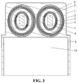
- two outer coil semi-conductive layers 3 are arranged side by side, as shown in FIG. 3 , to facilitate positioning and fixing of workpieces during an overall casting process.
- a side of the inner coil semi-conductive layer 5, close to the outer coil 4, and the upper and lower ends of the inner coil semi-conductive layer 5 are all cast with the insulating layer 2.
- an outer surface semi-conductive layer 1 is laid on the outside of the insulating layer 2.
- the inner coil 6, the inner coil semi-conductive layer 5, the outer coil 4 and the outer coil semi-conductive layer 3 are integrally cast to form a whole, and the integral casting material fills the periphery of these materials.
- the integrally cast insulating layer 2 may be formed by casting for one time or multiple times.
- the inner coil semi-conductive layer 5 and the outer surface semi-conductive layer 1 can be reliably connected to an integrally cast coil by means of spray coating, impregnation, pre-embedding, integrally casting, etc.
- the iron core 8 is installed after the inner coil 6 and the outer coil 4 have been manufactured.
- winding units are made of a relatively soft material.
- the inner coil semi-conductive layer 5 and the outer coil semi-conductive layer 3 may be semi-conductive tape made of high polymer materials, and the inner coil 6 and the outer coil 4 may be copper wires or the like which have desirable wettability with the casting material, and will not cause excessive mechanical stress concentration due to thermal expansion during the heating process. Cracking of the product is further avoided. A problem of cracking caused by excessive mechanical stress in the application process of conventional product, which is cast directly, is better solved.
- the coil and the semi-conductive material are integrally cast, and the iron core 8 is installed onto the insulating layer 2, which solves the problem of wire package cracking caused by the heating of the rigid material in a casting body.
- the windings are cast integrally, which has a relatively small mechanical stress, and the anti-cracking performance is greatly improved. Therefore, the safety of the transformer provided by the present disclosure is improved.
- an end of the outer surface semi-conductive layer 1 is pre-embedded inside the insulating layer 2, and is provided with an equipotential body 11 located inside the insulating layer 2.
- An end structure of the semi-conductive layer is pre-embedded to improve the distribution of electric field intensity at the end.
- the integrally cast wire package and transformer structure with an end grounding cut-off point structure, specifically, the equipotential body 11 is a bell mouth structure or a circular curvature structure to avoid local field strength concentration.
- the inner coil semi-conductive layer 5 and the iron core 8 are spaced to form an air flow channel 7.
- the air flow channel 7 around the iron core 8 passes through the inside of the transformer, which can better dissipate heat from the whole of the coil units and the iron core 8. Moreover, due to the presence of the inner coil semi-conductive layer 5, this part of the air flow channel 7 does not bear high field strength.
- the transformer further includes an equipotential cavity 10 fixedly connected to the insulating layer 2.
- the equipotential cavity 10 and the insulating layer 2 are formed integrally, and the equipotential cavity 10 and the insulating layer 2 are integrally cast.
- a structure of the equipotential cavity 10 is integrally formed.
- An inner surface semi-conductive layer 9 is provided inside the equipotential cavity 10.
- the iron core 8, the gap 7, the inner coil 6, the inner coil semi-conductive layer 5, and the outer surface semi-conductive layer 1 are located on one side of the insulating layer 2; and the outer coil 4, the outer coil semi-conductive layer 3, the inner surface semi-conductive layer 9 and the equipotential cavity 10 are on another side of the insulating layer 2.
- a transformer machining process is provided according to the present disclosure, which includes the following steps:
- the outer coil semi-conductive layer 3 and the inner coil semi-conductive layer 5 By providing the outer coil semi-conductive layer 3 and the inner coil semi-conductive layer 5, the problem of local excessive field strength caused by irregular coil structure is effectively solved, and the problem of wire package cracking caused by the heating of the rigid material in a casting body is solved. The safety of the transformer is improved.
- A3 arranging two coil units side by side, and casting an insulating medium on the two coil units to form an insulating layer 2.
- the insulating medium is uniformly cast on the inner coil 6, the outer coil 4, the outer coil semi-conductive layer 3 and the inner coil semi-conductive layer 5.
- the step A3 includes:
- one side of the outer semi-conductive layer 3 is tangent to an outer surface of an insulating layer 2 to facilitate positioning and fixing of workpieces during an overall casting process.
- A4 installing an iron core 8 onto the two coil units, and spacing the iron core 8 apart from the inner coil semi-conductive layer 5 to form an air flow channel 7.
- the air flow channel 7 around the iron core 8 passes through the inside of the transformer, which can better dissipate heat from the whole of the coil units and the iron core 8. Moreover, due to the presence of the inner coil semi-conductive layer 5, this part of the air flow channel 7 does not bear high field strength.
- an outer surface semi-conductive layer 1 is laid on the outside of the insulating layer 2.
- an end of the outer surface semi-conductive layer 1 is pre-embedded inside the insulating layer 2, and is provided with an equipotential body 11 located inside the insulating layer 2.
- An end structure of the semi-conductive layer is pre-embedded to improve the distribution of electric field intensity at the end.
- the integrally cast wire package and transformer structure with an end grounding cut-off point structure, specifically, the equipotential body 11 is a bell mouth structure or a circular curvature structure to avoid local field strength concentration.
- the transformer further includes an equipotential cavity 10 fixedly connected to the insulating layer 2.
- the equipotential cavity 10 and the insulating layer 2 are formed integrally, and the equipotential cavity 10 and the insulating layer 2 are integrally cast.
- a structure of the equipotential cavity 10 is integrally formed.
- An inner surface semi-conductive layer 9 is provided inside the equipotential cavity 10.
- the iron core 8, the gap 7, the inner coil 6, the inner coil semi-conductive layer 5, and the outer surface semi-conductive layer 1 are located on one side of the insulating layer 2; and the outer coil 4, the outer coil semi-conductive layer 3, the inner surface semi-conductive layer 9 and the equipotential cavity 10 are on another side of the insulating layer 2.
- winding units are made of a relatively soft material.
- the inner coil semi-conductive layer 5 and the outer coil semi-conductive layer 3 may be semi-conductive tape made of high polymer materials, and the inner coil 6 and the outer coil 4 may be copper wires or the like which have desirable wettability with the casting material, and will not cause excessive mechanical stress concentration due to thermal expansion during the heating process. Cracking of the product is further avoided. A problem of cracking caused by excessive mechanical stress in the application process of conventional product, which is cast directly, is better solved.
Landscapes
- Engineering & Computer Science (AREA)
- Power Engineering (AREA)
- Manufacturing & Machinery (AREA)
- Insulating Of Coils (AREA)
Abstract
Description
- This disclosure claims priority to
Chinese Patent Application No. 201911149325.5, titled "TRANSFORMER AND TRANSFORMER MACHINING PROCESS", filed with the China National Intellectual Property Administration on November 21, 2019 - The present disclosure relates to the technical field of electric equipment processing, and in particular to an epoxy-cast transformer and a transformer machining process.
- In an existing power distribution network, high-voltage electricity is provided to various loads after being stepped down by a power distribution transformer, which is a very important part of the power distribution network. Conventional power distribution transformer has many disadvantages, such as large size, heavy weight, large no-load loss, inability to automatically isolate faults, and output susceptible to interference from the power grid, etc.
- In a process of transformer machining, an iron core, a winding, and an insulating pad all need to be built into a casting material. Due to a large difference in thermal expansion coefficients of various materials, the casting material may crack due to thermal shock during an application process, which further leads to insulation failure. Moreover, the iron core generally has a rigid structure, which is difficult to solidify reliably with the casting material, and may also cause the casting material to crack in the application.
- Moreover, in the transformer, in order to ensure that a primary side and a secondary side can bear high voltage, field strength in the air must be less than a breakdown voltage of the transformer, which further leads to a larger distance between the primary and secondary sides, which affects a power density of the system to a certain extent. Excessive distance between the primary and secondary sides will cause excessive magnetic leakage, which increases the loss. An irregular coil structure will cause excessive local field strength, resulting in lower application safety of the transformer.
- Therefore, how to improve the application safety of the transformer is a technical issue to be solved urgently by those skilled in the art.
- An object of the present disclosure is to provide a transformer with improved application safety. Another object of the present disclosure is to provide a transformer machining process.
- In order to achieve the above objects, a transformer is provided according to the present disclosure, which includes two coil units arranged side by side. Each of the two coil units includes an inner coil and an outer coil sleeved outside the inner coil. The outer coil is wrapped with an outer coil semi-conductive layer, and the inner coil is wrapped with an inner coil semi-conductive layer. Each of the two coil units is integrally cast with an insulating layer.
- Preferably, an outer surface semi-conductive layer is laid on the outside of the insulating layer; an end of the outer surface semi-conductive layer is pre-embedded inside the insulating layer, and is provided with an equipotential body located inside the insulating layer.
- Preferably, the equipotential body is a bell mouth structure or a circular curvature structure.
- Preferably, the transformer further includes an iron core; the inner coil semi-conductive layer and the iron core are spaced to form an air flow channel.
- Preferably, the transformer further includes an equipotential cavity fixedly connected to the insulating layer; an inner surface semi-conductive layer is provided inside the equipotential cavity.
- Preferably, the equipotential cavity, the equipotential cavity and the insulating layer are integrally formed.
- Preferably, the transformer is a solid-state transformer.
- Preferably, the insulating layer includes a first insulating layer cast inside the outer surface semi-conductive layer, a second insulating layer cast inside the outer surface semi-conductive layer, and a third insulating layer cast on an outer surface of the outer surface semi-conductive layer and an outer surface of the outer surface semi-conductive layer.
- Preferably, the insulating layer is a casting structure formed integrally.
- A transformer machining process includes the following steps:
- A1: wrapping an inner coil semi-conductive layer outside an inner coil;
- A2: wrapping an outer coil semi-conductive layer outside an outer coil, and sleeving the outer coil outside the inner coil semi-conductive layer to form a coil unit;
- A3: arranging two coil units side by side, and casting an insulating medium on the two coil units to form an insulating layer; and
- A4: installing an iron core onto the two coil units, and spacing the iron core apart from the inner coil semi-conductive layer to form an air flow channel.
- Preferably, the step A3 includes:
- A31: casting a first insulating medium at a position of the inner coil wrapped with the inner coil semi-conductive layer; and casting a second insulating medium at a position of the outer coil wrapped with the outer coil semi-conductive layer; and
- A32: casting a third insulating medium on an outer surface of the inner coil semi-conductive layer and an outer surface of the outer coil semi-conductive layer, wherein the first insulating medium, the second insulating medium and the third insulating medium form the insulating layer.
- In the above technical solution, the transformer provided by the present disclosure includes two coil units arranged side by side. Each of the two coil units includes an inner coil and an outer coil sleeved outside the inner coil. The outer coil is wrapped with an outer coil semi-conductive layer, and the inner coil is wrapped with an inner coil semi-conductive layer. Each of the two coil units is integrally cast with an insulating layer.
- It can be seen from the above description that, in the transformer provided by the present disclosure, by providing the outer coil semi-conductive layer and the inner coil semi-conductive layer, a problem of excessive local field strength caused by an irregular coil structure can be effectively solved. Therefore, the safety of the transformer provided by the present disclosure is improved.
- For more clearly illustrating embodiments of the present disclosure or the technical solutions in the conventional technology, drawings referred to for describing the embodiments or the conventional technology will be briefly described hereinafter. Apparently, drawings in the following description are only examples of the present disclosure, and for the person skilled in the art, other drawings may be obtained based on the provided drawings without any creative efforts.
-
FIG. 1 is a schematic structural view of a transformer provided by an embodiment of the present disclosure; -
FIG. 2 is a front view of the transformer shown inFIG. 1 ; -
FIG. 3 is a top view of the transformer shown inFIG. 2 ; -
FIG. 4 is a side view of the transformer shown inFIG. 2 ; -
FIG. 5 is a schematic structural view of another transformer provided by an embodiment of the present disclosure; -
FIG. 6 is a front view of the transformer shown inFIG. 5 ; -
FIG. 7 is a top view of the transformer shown inFIG. 6 ; -
FIG. 8 is a side view of the transformer shown inFIG. 6 ; -
FIG. 9 is a schematic structural view of yet another transformer provided by an embodiment of the present disclosure; -
FIG. 10 is a front view of the transformer shown inFIG. 9 ; -
FIG. 11 is an enlarged view of part A shown inFIG. 10 ; -
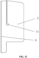
FIG. 12 is a view showing an installation position of an equipotential body provided by an embodiment of the present disclosure; and -
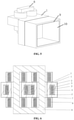
FIG. 13 is a view showing the mounting position of another equipotential body provided by an embodiment of the present disclosure. - Reference numerals in
FIGS. 1 to 13 are listed as follows:1 outer surface semi-conductive layer, 2 insulating layer, 3 outer coil semi-conductive layer, 4 outer coil, 5 inner coil semi-conductive layer, 6 inner coil, 7 air flow channel, 8 iron core, 9 inner surface semi-conductive layer, 10 equipotential cavity, 11 equipotential body. - A core of the present disclosure is to provide a transformer with improved application safety. Another core of the present disclosure is to provide a transformer machining process.
- In order to enable those skilled in the art to better understand the technical solutions of the present disclosure, the present disclosure will be further described in detail below with reference to the accompanying drawings and embodiments.
- Reference is made to
FIGS. 1 to 13 . - In a specific embodiment, the transformer provided by the specific embodiment of the present disclosure includes an
iron core 8 and two coil units arranged side by side. Each of the two coil units includes aninner coil 6 and anouter coil 4 sleeved outside theinner coil 6. Theouter coil 4 is wrapped with an outercoil semi-conductive layer 3. Theinner coil 6 is wrapped with an innercoil semi-conductive layer 5, which can effectively solve the problem of excessive local field strength caused by the irregular structure of theinner coil 6. Preferably, one side of theouter semi-conductive layer 3 is tangent to an outer surface of an insulatinglayer 2 to facilitate positioning and fixing of workpieces during an overall casting process. - Each of the two coil units is integrally cast with the insulating
layer 2. High electric field strength of the transformer is coupled in thecast insulating layer 2. Specifically, the insulatinglayer 2 is an integral casting structure, that is, the inner coil, the outer coil, the outercoil semi-conductive layer 3 and the innercoil semi-conductive layer 5 are insulation cast at the same time. - The insulating
layer 2 includes a first insulating layer cast inside an outersurface semi-conductive layer 1, a second insulating layer cast inside the outersurface semi-conductive layer 1, and a third insulating layer cast on an outer surface of the outersurface semi-conductive layer 1 and an outer surface of the outersurface semi-conductive layer 1. That is, a wire package of the inner coil, a wire package of the outer coil and an external insulation structure are respectively cast. Preferably, the materials of the first insulating layer, the second insulating layer and the third insulating layer are the same. - Since a semi-conductive material has desirable wettability with an insulation casting material of the insulating layer, the field strength can be concentrated inside the insulating
layer 2. The breakdown field strength of a general casting material is greater than 20kV/mm, which can effectively reduce a distance between the primary and secondary sides, improve the power density and reduce the magnetic leakage. - Specifically, the transformer provided in the present disclosure may specifically be a solid-state transformer.
- Specifically, as shown in
FIG. 3 andFIG. 4 , theouter coil 4 may be sleeved outside theinner coil 6. In another way, as shown inFIG. 5 to FIG. 8 , theinner coil 6 and theouter coil 4 may arranged as an up and down structure, and theinner coil 6 and theouter coil 4 of the upper and down structure may be cast integrally or separately. The illustrated embodiment is an example of separate casting. - In a specific embodiment, two outer
coil semi-conductive layers 3 are arranged side by side, as shown inFIG. 3 , to facilitate positioning and fixing of workpieces during an overall casting process. - Specifically, as shown in
FIG. 2 , a side of the innercoil semi-conductive layer 5, close to theouter coil 4, and the upper and lower ends of the innercoil semi-conductive layer 5 are all cast with the insulatinglayer 2. In a specific embodiment, an outersurface semi-conductive layer 1 is laid on the outside of the insulatinglayer 2. - The
inner coil 6, the innercoil semi-conductive layer 5, theouter coil 4 and the outercoil semi-conductive layer 3 are integrally cast to form a whole, and the integral casting material fills the periphery of these materials. The integrally cast insulatinglayer 2 may be formed by casting for one time or multiple times. The innercoil semi-conductive layer 5 and the outersurface semi-conductive layer 1 can be reliably connected to an integrally cast coil by means of spray coating, impregnation, pre-embedding, integrally casting, etc. - Specifically, the
iron core 8 is installed after theinner coil 6 and theouter coil 4 have been manufactured. - Preferably, winding units are made of a relatively soft material. Specifically, the inner
coil semi-conductive layer 5 and the outercoil semi-conductive layer 3 may be semi-conductive tape made of high polymer materials, and theinner coil 6 and theouter coil 4 may be copper wires or the like which have desirable wettability with the casting material, and will not cause excessive mechanical stress concentration due to thermal expansion during the heating process. Cracking of the product is further avoided. A problem of cracking caused by excessive mechanical stress in the application process of conventional product, which is cast directly, is better solved. - It can be seen from the above description that, in the transformer provided by the specific embodiment of the present disclosure, the coil and the semi-conductive material are integrally cast, and the
iron core 8 is installed onto the insulatinglayer 2, which solves the problem of wire package cracking caused by the heating of the rigid material in a casting body. The windings are cast integrally, which has a relatively small mechanical stress, and the anti-cracking performance is greatly improved. Therefore, the safety of the transformer provided by the present disclosure is improved. - In a specific embodiment, an end of the outer
surface semi-conductive layer 1 is pre-embedded inside the insulatinglayer 2, and is provided with anequipotential body 11 located inside the insulatinglayer 2. An end structure of the semi-conductive layer is pre-embedded to improve the distribution of electric field intensity at the end. The integrally cast wire package and transformer structure with an end grounding cut-off point structure, specifically, theequipotential body 11 is a bell mouth structure or a circular curvature structure to avoid local field strength concentration. - In a specific embodiment, the inner
coil semi-conductive layer 5 and theiron core 8 are spaced to form anair flow channel 7. Theair flow channel 7 around theiron core 8 passes through the inside of the transformer, which can better dissipate heat from the whole of the coil units and theiron core 8. Moreover, due to the presence of the innercoil semi-conductive layer 5, this part of theair flow channel 7 does not bear high field strength. - On the basis of the above solutions, preferably, the transformer further includes an
equipotential cavity 10 fixedly connected to the insulatinglayer 2. Preferably, theequipotential cavity 10 and the insulatinglayer 2 are formed integrally, and theequipotential cavity 10 and the insulatinglayer 2 are integrally cast. A structure of theequipotential cavity 10 is integrally formed. An innersurface semi-conductive layer 9 is provided inside theequipotential cavity 10. By providing theequipotential cavity 10, the space utilization rate is effectively improved, and the power density is improved. By providing theequipotential cavity 10, requirement of the conventional transformer adopts high-voltage lead-out terminal to achieve the insulation distance is changed. No other objects are allowed to be placed in the space. However, with the present solution, related electronic components on the same side may be placed inside theequipotential cavity 10, so as to avoid the insulation failure of the device due to excessive field strength. - In a specific embodiment, the
iron core 8, thegap 7, theinner coil 6, the innercoil semi-conductive layer 5, and the outersurface semi-conductive layer 1 are located on one side of the insulatinglayer 2; and theouter coil 4, the outercoil semi-conductive layer 3, the innersurface semi-conductive layer 9 and theequipotential cavity 10 are on another side of the insulatinglayer 2. - A transformer machining process is provided according to the present disclosure, which includes the following steps:
- A1: wrapping an inner
coil semi-conductive layer 5 outside aninner coil 6; - A2: wrapping an outer
coil semi-conductive layer 3 outside anouter coil 4, and sleeving theouter coil 4 outside the innercoil semi-conductive layer 5 to form a coil unit; - By providing the outer
coil semi-conductive layer 3 and the innercoil semi-conductive layer 5, the problem of local excessive field strength caused by irregular coil structure is effectively solved, and the problem of wire package cracking caused by the heating of the rigid material in a casting body is solved. The safety of the transformer is improved. - A3: arranging two coil units side by side, and casting an insulating medium on the two coil units to form an insulating
layer 2. The insulating medium is uniformly cast on theinner coil 6, theouter coil 4, the outercoil semi-conductive layer 3 and the innercoil semi-conductive layer 5. - Specifically, the step A3 includes:
- A31: casting a first insulating medium at a position of the
inner coil 6 wrapped with the innercoil semi-conductive layer 5; and casting a second insulating medium at a position of theouter coil 4 wrapped with the outercoil semi-conductive layer 3. That is, theinner coil 6 and theouter coil 4 are separately cast. - A32: casting a third insulating medium on an outer surface of the inner
coil semi-conductive layer 5 and an outer surface of the outercoil semi-conductive layer 3, wherein the first insulating medium, the second insulating medium and the third insulating medium form the insulating layer. Preferably, the first insulating medium, the second insulating medium and the third insulating medium are the same insulating medium. - Preferably, one side of the
outer semi-conductive layer 3 is tangent to an outer surface of an insulatinglayer 2 to facilitate positioning and fixing of workpieces during an overall casting process. - A4: installing an
iron core 8 onto the two coil units, and spacing theiron core 8 apart from the innercoil semi-conductive layer 5 to form anair flow channel 7. Theair flow channel 7 around theiron core 8 passes through the inside of the transformer, which can better dissipate heat from the whole of the coil units and theiron core 8. Moreover, due to the presence of the innercoil semi-conductive layer 5, this part of theair flow channel 7 does not bear high field strength. - In a specific embodiment, an outer
surface semi-conductive layer 1 is laid on the outside of the insulatinglayer 2. In a specific embodiment, an end of the outersurface semi-conductive layer 1 is pre-embedded inside the insulatinglayer 2, and is provided with anequipotential body 11 located inside the insulatinglayer 2. An end structure of the semi-conductive layer is pre-embedded to improve the distribution of electric field intensity at the end. The integrally cast wire package and transformer structure with an end grounding cut-off point structure, specifically, theequipotential body 11 is a bell mouth structure or a circular curvature structure to avoid local field strength concentration. - On the basis of the above solutions, preferably, the transformer further includes an
equipotential cavity 10 fixedly connected to the insulatinglayer 2. Preferably, theequipotential cavity 10 and the insulatinglayer 2 are formed integrally, and theequipotential cavity 10 and the insulatinglayer 2 are integrally cast. A structure of theequipotential cavity 10 is integrally formed. An innersurface semi-conductive layer 9 is provided inside theequipotential cavity 10. By providing theequipotential cavity 10, the space utilization rate is effectively improved, and the power density is improved. By providing theequipotential cavity 10, requirement of the conventional transformer adopts high-voltage lead-out terminal to achieve the insulation distance is changed. No other objects are allowed to be placed in the space. However, with the present solution, related electronic components on the same side may be placed inside theequipotential cavity 10, so as to avoid the insulation failure of the device due to excessive field strength. - In a specific embodiment, the
iron core 8, thegap 7, theinner coil 6, the innercoil semi-conductive layer 5, and the outersurface semi-conductive layer 1 are located on one side of the insulatinglayer 2; and theouter coil 4, the outercoil semi-conductive layer 3, the innersurface semi-conductive layer 9 and theequipotential cavity 10 are on another side of the insulatinglayer 2. - Preferably, winding units are made of a relatively soft material. Specifically, the inner
coil semi-conductive layer 5 and the outercoil semi-conductive layer 3 may be semi-conductive tape made of high polymer materials, and theinner coil 6 and theouter coil 4 may be copper wires or the like which have desirable wettability with the casting material, and will not cause excessive mechanical stress concentration due to thermal expansion during the heating process. Cracking of the product is further avoided. A problem of cracking caused by excessive mechanical stress in the application process of conventional product, which is cast directly, is better solved. - The embodiments of the present disclosure are described in a progressive manner, with an emphasis placed on explaining the difference between each embodiment and other embodiments. The same or similar parts among the embodiments can be referred to each other.
- Based on the above description of the disclosed embodiments, those skilled in the art can implement or deploy the present application. Various modifications to these embodiments are obvious to a person skilled in the art, the general principle defined herein may be implemented in other embodiments without departing from the spirit and scope of the present application. Hence, the present application is not limited to the embodiments disclosed herein, but is to conform to the widest scope in accordance with the principle and novel features disclosed herein.
Claims (11)
- A transformer, comprising two coil units arranged side by side, wherein each of the two coil units comprises an inner coil (6) and an outer coil (4) sleeved outside the inner coil (6), the outer coil (4) is wrapped with an outer coil semi-conductive layer (3), the inner coil (6) is wrapped with an inner coil semi-conductive layer (5), and each of the two coil units is integrally cast with an insulating layer (2).
- The transformer according to claim 1, wherein an outer surface semi-conductive layer (1) is laid on an outside of the insulating layer (1); an end of the outer surface semi-conductive layer (1) is pre-embedded inside the insulating layer (2), and is provided with an equipotential body (11) located inside the insulating layer (2).
- The transformer according to claim 2, wherein the equipotential body (11) is a bell mouth structure or a circular curvature structure.
- The transformer according to claim 1, further comprising an iron core (8), wherein the inner coil semi-conductive layer (5) and the iron core (8) are spaced to form an air flow channel (7).
- The transformer according to claim 1, further comprising an equipotential cavity (10) fixedly connected to the insulating layer (2), wherein an inner surface semi-conductive layer (9) is provided inside the equipotential cavity (10).
- The transformer according to claim 5, wherein the equipotential cavity (10), the equipotential cavity (10) and the insulating layer (2) are integrally formed.
- The transformer according to claim 1, wherein the transformer is a solid-state transformer.
- The transformer according to claim 2 or 3, wherein the insulating layer (2) comprises a first insulating layer cast inside the outer surface semi-conductive layer (1), a second insulating layer cast inside the outer surface semi-conductive layer (1), and a third insulating layer cast on an outer surface of the outer surface semi-conductive layer (1) and an outer surface of the outer surface semi-conductive layer (1).
- The transformer according to any one of claims 1 to 7, wherein the insulating layer (2) is a casting structure formed integrally.
- A transformer machining process, comprising the following steps:A1: wrapping an inner coil semi-conductive layer (5) outside an inner coil (6);A2: wrapping an outer coil semi-conductive layer (3) outside an outer coil (4), and sleeving the outer coil (4) outside the inner coil semi-conductive layer (5) to form a coil unit;A3: arranging two coil units side by side, and casting an insulating medium on the two coil units to form an insulating layer (2); andA4: installing an iron core (8) onto the two coil units, and spacing the iron core (8) apart from the inner coil semi-conductive layer (5) to form an air flow channel (7).
- The transformer machining process according to claim 10, wherein the step A3 comprises:A31: casting a first insulating medium at a position of the inner coil wrapped with the inner coil semi-conductive layer; and casting a second insulating medium at a position of the outer coil wrapped with the outer coil semi-conductive layer; andA32: casting a third insulating medium on an outer surface of the inner coil semi-conductive layer and an outer surface of the outer coil semi-conductive layer, wherein the first insulating medium, the second insulating medium and the third insulating medium form the insulating layer.
Applications Claiming Priority (2)
| Application Number | Priority Date | Filing Date | Title |
|---|---|---|---|
| CN201911149325.5A CN110853898A (en) | 2019-11-21 | 2019-11-21 | Transformer and Transformer Processing Technology |
| PCT/CN2020/093090 WO2021098181A1 (en) | 2019-11-21 | 2020-05-29 | Transformer and transformer machining process |
Publications (4)
| Publication Number | Publication Date |
|---|---|
| EP3951813A1 true EP3951813A1 (en) | 2022-02-09 |
| EP3951813A4 EP3951813A4 (en) | 2023-01-18 |
| EP3951813B1 EP3951813B1 (en) | 2025-04-02 |
| EP3951813C0 EP3951813C0 (en) | 2025-04-02 |
Family
ID=69603422
Family Applications (1)
| Application Number | Title | Priority Date | Filing Date |
|---|---|---|---|
| EP20890627.1A Active EP3951813B1 (en) | 2019-11-21 | 2020-05-29 | Transformer and transformer machining process |
Country Status (5)
| Country | Link |
|---|---|
| US (1) | US12381034B2 (en) |
| EP (1) | EP3951813B1 (en) |
| JP (1) | JP7263549B2 (en) |
| CN (1) | CN110853898A (en) |
| WO (1) | WO2021098181A1 (en) |
Cited By (1)
| Publication number | Priority date | Publication date | Assignee | Title |
|---|---|---|---|---|
| EP4345854A1 (en) * | 2022-09-30 | 2024-04-03 | ABB Schweiz AG | Transformer coil |
Families Citing this family (4)
| Publication number | Priority date | Publication date | Assignee | Title |
|---|---|---|---|---|
| CN110853898A (en) | 2019-11-21 | 2020-02-28 | 阳光电源股份有限公司 | Transformer and Transformer Processing Technology |
| CN111986883B (en) * | 2020-06-19 | 2022-11-15 | 阳光电源股份有限公司 | Solid-state transformer and preparation method thereof |
| CN112652470B (en) * | 2020-12-07 | 2022-11-15 | 阳光电源股份有限公司 | a transformer |
| CN115020087A (en) * | 2021-03-04 | 2022-09-06 | 南京南瑞继保电气有限公司 | Dry-type high-frequency transformer and processing technology |
Family Cites Families (19)
| Publication number | Priority date | Publication date | Assignee | Title |
|---|---|---|---|---|
| JPS5268918A (en) * | 1975-12-05 | 1977-06-08 | Hitachi Ltd | Insulated transformer |
| JPH06314626A (en) * | 1993-04-30 | 1994-11-08 | Hirai Denkeiki Kk | Winding type current transformer |
| JP3533252B2 (en) * | 1995-02-09 | 2004-05-31 | 株式会社東芝 | Transformer |
| AU718707B2 (en) * | 1996-05-29 | 2000-04-20 | Abb Ab | Insulated conductor for high-voltage windings and a method of manufacturing the same |
| SE9704423D0 (en) * | 1997-02-03 | 1997-11-28 | Asea Brown Boveri | Rotary electric machine with flushing support |
| SE512060C2 (en) | 1997-02-03 | 2000-01-17 | Abb Ab | Winding, process for making such and power transformer or reactor |
| JP3969492B2 (en) * | 2003-07-08 | 2007-09-05 | 株式会社アイキューフォー | High voltage transformer and conductive coating single mold coil for the high voltage transformer |
| DE102005015785A1 (en) * | 2005-04-01 | 2006-11-16 | Siemens Ag | Transformer with electrical shielding |
| DE102007006005B3 (en) * | 2007-02-07 | 2008-07-31 | Volker Werner Hanser | High-voltage transformer, has high- and low-voltage coils, between which high-voltage insulation is provided, and electrically conductive layers placed on defined potentials, which are same or close to high and low-voltages, respectively |
| KR100927685B1 (en) * | 2008-09-01 | 2009-11-20 | 제룡산업 주식회사 | Manufacturing method of underground buried solid isolation transformer |
| KR101028054B1 (en) * | 2009-04-10 | 2011-04-08 | 제룡산업 주식회사 | Fully solid insulated mold transformer and manufacturing method thereof |
| US20150109090A1 (en) * | 2013-10-21 | 2015-04-23 | Hammond Power Solutions, Inc. | Electrical transformer with a shielded cast coil assembly |
| EP3364430A1 (en) * | 2017-02-17 | 2018-08-22 | ABB Schweiz AG | Medium-frequency transformer with dry core |
| WO2019232763A1 (en) * | 2018-06-07 | 2019-12-12 | Siemens Aktiengesellschaft | Shielded coil assemblies and methods for dry-type transformers |
| CN108831721B (en) * | 2018-06-27 | 2020-03-24 | 阳光电源股份有限公司 | Transformer insulation components and transformers |
| CN109524220B (en) * | 2018-12-27 | 2020-08-28 | 阳光电源股份有限公司 | Transformer and Transformer Processing Method |
| EP3770931B1 (en) * | 2019-07-23 | 2024-12-18 | Solaredge Technologies Ltd. | Transformer apparatus |
| CN211376390U (en) * | 2019-11-21 | 2020-08-28 | 阳光电源股份有限公司 | transformer |
| CN110853898A (en) * | 2019-11-21 | 2020-02-28 | 阳光电源股份有限公司 | Transformer and Transformer Processing Technology |
-
2019
- 2019-11-21 CN CN201911149325.5A patent/CN110853898A/en active Pending
-
2020
- 2020-05-29 EP EP20890627.1A patent/EP3951813B1/en active Active
- 2020-05-29 US US17/601,920 patent/US12381034B2/en active Active
- 2020-05-29 WO PCT/CN2020/093090 patent/WO2021098181A1/en not_active Ceased
- 2020-05-29 JP JP2021559672A patent/JP7263549B2/en active Active
Cited By (1)
| Publication number | Priority date | Publication date | Assignee | Title |
|---|---|---|---|---|
| EP4345854A1 (en) * | 2022-09-30 | 2024-04-03 | ABB Schweiz AG | Transformer coil |
Also Published As
| Publication number | Publication date |
|---|---|
| US20220148797A1 (en) | 2022-05-12 |
| US12381034B2 (en) | 2025-08-05 |
| JP7263549B2 (en) | 2023-04-24 |
| EP3951813A4 (en) | 2023-01-18 |
| JP2022527119A (en) | 2022-05-30 |
| EP3951813B1 (en) | 2025-04-02 |
| WO2021098181A1 (en) | 2021-05-27 |
| EP3951813C0 (en) | 2025-04-02 |
| CN110853898A (en) | 2020-02-28 |
Similar Documents
| Publication | Publication Date | Title |
|---|---|---|
| US12381034B2 (en) | Transformer and transformer machining process | |
| CN201134338Y (en) | High voltage transformer with shielding ring and shielding ring | |
| CN103069515B (en) | In winding, there is the transformer of shading ring | |
| EP3109873B1 (en) | Inductor coil and electromagnetic component | |
| US10700564B2 (en) | Manufacturing method for a conductor disposed within an insulator | |
| CN211376390U (en) | transformer | |
| CN116936243A (en) | High-voltage winding and dry-type transformer | |
| JP4794999B2 (en) | Lightning proof type low voltage insulation transformer | |
| CN105047381B (en) | A kind of 35kV dry-type air-core reactors | |
| US11610716B2 (en) | Transformer | |
| JP5849617B2 (en) | Mold current transformer | |
| CN109524220B (en) | Transformer and Transformer Processing Method | |
| EP4197012B1 (en) | Transformer comprising winding | |
| EP4099348A2 (en) | Dry-type transformer and winding method thereof | |
| WO2016070393A1 (en) | Cooling method and apparatus for forced-directed cooling mixing type transformer winding | |
| CN103595166B (en) | A kind of low center height large-size machine | |
| CN112164562B (en) | Insulation tool and insulation method for satellite-borne miniaturized high-voltage transformer | |
| CN203607956U (en) | Low-center high-capacity motor | |
| JP5317930B2 (en) | Static induction machine | |
| JP2001223125A (en) | Electrostatic shield and electrostatic shield device for induction equipment | |
| CN120600487A (en) | Semi-potted grounded Litz wire shielded high voltage and high frequency transformer structure | |
| CN202285191U (en) | High-voltage coil of dry type transformer for photovoltaic generation | |
| KR20110081192A (en) | Transformers | |
| CN120108898A (en) | A high-frequency high-voltage transformer and its control method, and electric energy conversion structure | |
| CN118780021A (en) | A reactor coil design method and ±800kV dry-type bridge arm reactor |
Legal Events
| Date | Code | Title | Description |
|---|---|---|---|
| STAA | Information on the status of an ep patent application or granted ep patent |
Free format text: STATUS: THE INTERNATIONAL PUBLICATION HAS BEEN MADE |
|
| PUAI | Public reference made under article 153(3) epc to a published international application that has entered the european phase |
Free format text: ORIGINAL CODE: 0009012 |
|
| STAA | Information on the status of an ep patent application or granted ep patent |
Free format text: STATUS: REQUEST FOR EXAMINATION WAS MADE |
|
| 17P | Request for examination filed |
Effective date: 20211129 |
|
| AK | Designated contracting states |
Kind code of ref document: A1 Designated state(s): AL AT BE BG CH CY CZ DE DK EE ES FI FR GB GR HR HU IE IS IT LI LT LU LV MC MK MT NL NO PL PT RO RS SE SI SK SM TR |
|
| A4 | Supplementary search report drawn up and despatched |
Effective date: 20221216 |
|
| RIC1 | Information provided on ipc code assigned before grant |
Ipc: H01F 41/12 20060101ALI20221212BHEP Ipc: H01F 27/32 20060101AFI20221212BHEP |
|
| DAV | Request for validation of the european patent (deleted) | ||
| DAX | Request for extension of the european patent (deleted) | ||
| GRAP | Despatch of communication of intention to grant a patent |
Free format text: ORIGINAL CODE: EPIDOSNIGR1 |
|
| STAA | Information on the status of an ep patent application or granted ep patent |
Free format text: STATUS: GRANT OF PATENT IS INTENDED |
|
| INTG | Intention to grant announced |
Effective date: 20241028 |
|
| GRAS | Grant fee paid |
Free format text: ORIGINAL CODE: EPIDOSNIGR3 |
|
| GRAA | (expected) grant |
Free format text: ORIGINAL CODE: 0009210 |
|
| STAA | Information on the status of an ep patent application or granted ep patent |
Free format text: STATUS: THE PATENT HAS BEEN GRANTED |
|
| AK | Designated contracting states |
Kind code of ref document: B1 Designated state(s): AL AT BE BG CH CY CZ DE DK EE ES FI FR GB GR HR HU IE IS IT LI LT LU LV MC MK MT NL NO PL PT RO RS SE SI SK SM TR |
|
| REG | Reference to a national code |
Ref country code: GB Ref legal event code: FG4D |
|
| REG | Reference to a national code |
Ref country code: CH Ref legal event code: EP |
|
| REG | Reference to a national code |
Ref country code: IE Ref legal event code: FG4D |
|
| REG | Reference to a national code |
Ref country code: DE Ref legal event code: R096 Ref document number: 602020048900 Country of ref document: DE |
|
| U01 | Request for unitary effect filed |
Effective date: 20250416 |
|
| U07 | Unitary effect registered |
Designated state(s): AT BE BG DE DK EE FI FR IT LT LU LV MT NL PT RO SE SI Effective date: 20250424 |
|
| U20 | Renewal fee for the european patent with unitary effect paid |
Year of fee payment: 6 Effective date: 20250506 |
|
| PG25 | Lapsed in a contracting state [announced via postgrant information from national office to epo] |
Ref country code: ES Free format text: LAPSE BECAUSE OF FAILURE TO SUBMIT A TRANSLATION OF THE DESCRIPTION OR TO PAY THE FEE WITHIN THE PRESCRIBED TIME-LIMIT Effective date: 20250402 |
|
| PG25 | Lapsed in a contracting state [announced via postgrant information from national office to epo] |
Ref country code: NO Free format text: LAPSE BECAUSE OF FAILURE TO SUBMIT A TRANSLATION OF THE DESCRIPTION OR TO PAY THE FEE WITHIN THE PRESCRIBED TIME-LIMIT Effective date: 20250702 Ref country code: GR Free format text: LAPSE BECAUSE OF FAILURE TO SUBMIT A TRANSLATION OF THE DESCRIPTION OR TO PAY THE FEE WITHIN THE PRESCRIBED TIME-LIMIT Effective date: 20250703 |
|
| PG25 | Lapsed in a contracting state [announced via postgrant information from national office to epo] |
Ref country code: PL Free format text: LAPSE BECAUSE OF FAILURE TO SUBMIT A TRANSLATION OF THE DESCRIPTION OR TO PAY THE FEE WITHIN THE PRESCRIBED TIME-LIMIT Effective date: 20250402 |
|
| PG25 | Lapsed in a contracting state [announced via postgrant information from national office to epo] |
Ref country code: HR Free format text: LAPSE BECAUSE OF FAILURE TO SUBMIT A TRANSLATION OF THE DESCRIPTION OR TO PAY THE FEE WITHIN THE PRESCRIBED TIME-LIMIT Effective date: 20250402 |
|
| PG25 | Lapsed in a contracting state [announced via postgrant information from national office to epo] |
Ref country code: RS Free format text: LAPSE BECAUSE OF FAILURE TO SUBMIT A TRANSLATION OF THE DESCRIPTION OR TO PAY THE FEE WITHIN THE PRESCRIBED TIME-LIMIT Effective date: 20250702 |
|
| PG25 | Lapsed in a contracting state [announced via postgrant information from national office to epo] |
Ref country code: IS Free format text: LAPSE BECAUSE OF FAILURE TO SUBMIT A TRANSLATION OF THE DESCRIPTION OR TO PAY THE FEE WITHIN THE PRESCRIBED TIME-LIMIT Effective date: 20250802 |
|
| REG | Reference to a national code |
Ref country code: CH Ref legal event code: H13 Free format text: ST27 STATUS EVENT CODE: U-0-0-H10-H13 (AS PROVIDED BY THE NATIONAL OFFICE) Effective date: 20251223 |
|
| PG25 | Lapsed in a contracting state [announced via postgrant information from national office to epo] |
Ref country code: SM Free format text: LAPSE BECAUSE OF FAILURE TO SUBMIT A TRANSLATION OF THE DESCRIPTION OR TO PAY THE FEE WITHIN THE PRESCRIBED TIME-LIMIT Effective date: 20250402 |
|
| PG25 | Lapsed in a contracting state [announced via postgrant information from national office to epo] |
Ref country code: CH Free format text: LAPSE BECAUSE OF NON-PAYMENT OF DUE FEES Effective date: 20250531 |
|
| PG25 | Lapsed in a contracting state [announced via postgrant information from national office to epo] |
Ref country code: CZ Free format text: LAPSE BECAUSE OF FAILURE TO SUBMIT A TRANSLATION OF THE DESCRIPTION OR TO PAY THE FEE WITHIN THE PRESCRIBED TIME-LIMIT Effective date: 20250402 |
|
| PG25 | Lapsed in a contracting state [announced via postgrant information from national office to epo] |
Ref country code: SK Free format text: LAPSE BECAUSE OF FAILURE TO SUBMIT A TRANSLATION OF THE DESCRIPTION OR TO PAY THE FEE WITHIN THE PRESCRIBED TIME-LIMIT Effective date: 20250402 |
|
| PG25 | Lapsed in a contracting state [announced via postgrant information from national office to epo] |
Ref country code: MC Free format text: LAPSE BECAUSE OF FAILURE TO SUBMIT A TRANSLATION OF THE DESCRIPTION OR TO PAY THE FEE WITHIN THE PRESCRIBED TIME-LIMIT Effective date: 20250402 |
|
| PLBE | No opposition filed within time limit |
Free format text: ORIGINAL CODE: 0009261 |
|
| STAA | Information on the status of an ep patent application or granted ep patent |
Free format text: STATUS: NO OPPOSITION FILED WITHIN TIME LIMIT |
|
| REG | Reference to a national code |
Ref country code: CH Ref legal event code: L10 Free format text: ST27 STATUS EVENT CODE: U-0-0-L10-L00 (AS PROVIDED BY THE NATIONAL OFFICE) Effective date: 20260211 |
|
| 26N | No opposition filed |
Effective date: 20260105 |
|
| GBPC | Gb: european patent ceased through non-payment of renewal fee |
Effective date: 20250702 |
|
| PG25 | Lapsed in a contracting state [announced via postgrant information from national office to epo] |
Ref country code: GB Free format text: LAPSE BECAUSE OF NON-PAYMENT OF DUE FEES Effective date: 20250702 |
|
| PG25 | Lapsed in a contracting state [announced via postgrant information from national office to epo] |
Ref country code: IE Free format text: LAPSE BECAUSE OF NON-PAYMENT OF DUE FEES Effective date: 20250529 |