EP3951550A1 - Voltage regulator with hybrid control for fast transient response - Google Patents
Voltage regulator with hybrid control for fast transient response Download PDFInfo
- Publication number
- EP3951550A1 EP3951550A1 EP21189705.3A EP21189705A EP3951550A1 EP 3951550 A1 EP3951550 A1 EP 3951550A1 EP 21189705 A EP21189705 A EP 21189705A EP 3951550 A1 EP3951550 A1 EP 3951550A1
- Authority
- EP
- European Patent Office
- Prior art keywords
- current
- voltage
- output
- control circuit
- voltage regulator
- Prior art date
- Legal status (The legal status is an assumption and is not a legal conclusion. Google has not performed a legal analysis and makes no representation as to the accuracy of the status listed.)
- Granted
Links
Images


Classifications
-
- G—PHYSICS
- G05—CONTROLLING; REGULATING
- G05F—SYSTEMS FOR REGULATING ELECTRIC OR MAGNETIC VARIABLES
- G05F1/00—Automatic systems in which deviations of an electric quantity from one or more predetermined values are detected at the output of the system and fed back to a device within the system to restore the detected quantity to its predetermined value or values, i.e. retroactive systems
- G05F1/10—Regulating voltage or current
- G05F1/46—Regulating voltage or current wherein the variable actually regulated by the final control device is DC
- G05F1/56—Regulating voltage or current wherein the variable actually regulated by the final control device is DC using semiconductor devices in series with the load as final control devices
- G05F1/565—Regulating voltage or current wherein the variable actually regulated by the final control device is DC using semiconductor devices in series with the load as final control devices sensing a condition of the system or its load in addition to means responsive to deviations in the output of the system, e.g. current, voltage, power factor
-
- H—ELECTRICITY
- H02—GENERATION; CONVERSION OR DISTRIBUTION OF ELECTRIC POWER
- H02M—APPARATUS FOR CONVERSION BETWEEN AC AND AC, BETWEEN AC AND DC, OR BETWEEN DC AND DC, AND FOR USE WITH MAINS OR SIMILAR POWER SUPPLY SYSTEMS; CONVERSION OF DC OR AC INPUT POWER INTO SURGE OUTPUT POWER; CONTROL OR REGULATION THEREOF
- H02M3/00—Conversion of DC power input into DC power output
- H02M3/02—Conversion of DC power input into DC power output without intermediate conversion into AC
- H02M3/04—Conversion of DC power input into DC power output without intermediate conversion into AC by static converters
- H02M3/10—Conversion of DC power input into DC power output without intermediate conversion into AC by static converters using discharge tubes with control electrode or semiconductor devices with control electrode
- H02M3/145—Conversion of DC power input into DC power output without intermediate conversion into AC by static converters using discharge tubes with control electrode or semiconductor devices with control electrode using devices of a triode or transistor type requiring continuous application of a control signal
- H02M3/155—Conversion of DC power input into DC power output without intermediate conversion into AC by static converters using discharge tubes with control electrode or semiconductor devices with control electrode using devices of a triode or transistor type requiring continuous application of a control signal using semiconductor devices only
- H02M3/156—Conversion of DC power input into DC power output without intermediate conversion into AC by static converters using discharge tubes with control electrode or semiconductor devices with control electrode using devices of a triode or transistor type requiring continuous application of a control signal using semiconductor devices only with automatic control of output voltage or current, e.g. switching regulators
- H02M3/158—Conversion of DC power input into DC power output without intermediate conversion into AC by static converters using discharge tubes with control electrode or semiconductor devices with control electrode using devices of a triode or transistor type requiring continuous application of a control signal using semiconductor devices only with automatic control of output voltage or current, e.g. switching regulators including plural semiconductor devices as final control devices for a single load
-
- G—PHYSICS
- G05—CONTROLLING; REGULATING
- G05F—SYSTEMS FOR REGULATING ELECTRIC OR MAGNETIC VARIABLES
- G05F1/00—Automatic systems in which deviations of an electric quantity from one or more predetermined values are detected at the output of the system and fed back to a device within the system to restore the detected quantity to its predetermined value or values, i.e. retroactive systems
- G05F1/10—Regulating voltage or current
- G05F1/46—Regulating voltage or current wherein the variable actually regulated by the final control device is DC
- G05F1/56—Regulating voltage or current wherein the variable actually regulated by the final control device is DC using semiconductor devices in series with the load as final control devices
- G05F1/561—Voltage to current converters
-
- G—PHYSICS
- G05—CONTROLLING; REGULATING
- G05F—SYSTEMS FOR REGULATING ELECTRIC OR MAGNETIC VARIABLES
- G05F1/00—Automatic systems in which deviations of an electric quantity from one or more predetermined values are detected at the output of the system and fed back to a device within the system to restore the detected quantity to its predetermined value or values, i.e. retroactive systems
- G05F1/10—Regulating voltage or current
- G05F1/46—Regulating voltage or current wherein the variable actually regulated by the final control device is DC
- G05F1/56—Regulating voltage or current wherein the variable actually regulated by the final control device is DC using semiconductor devices in series with the load as final control devices
- G05F1/575—Regulating voltage or current wherein the variable actually regulated by the final control device is DC using semiconductor devices in series with the load as final control devices characterised by the feedback circuit
-
- H—ELECTRICITY
- H03—ELECTRONIC CIRCUITRY
- H03F—AMPLIFIERS
- H03F1/00—Details of amplifiers with only discharge tubes, only semiconductor devices or only unspecified devices as amplifying elements
- H03F1/02—Modifications of amplifiers to raise the efficiency, e.g. gliding Class A stages, use of an auxiliary oscillation
- H03F1/0205—Modifications of amplifiers to raise the efficiency, e.g. gliding Class A stages, use of an auxiliary oscillation in transistor amplifiers
- H03F1/0211—Modifications of amplifiers to raise the efficiency, e.g. gliding Class A stages, use of an auxiliary oscillation in transistor amplifiers with control of the supply voltage or current
-
- H—ELECTRICITY
- H02—GENERATION; CONVERSION OR DISTRIBUTION OF ELECTRIC POWER
- H02M—APPARATUS FOR CONVERSION BETWEEN AC AND AC, BETWEEN AC AND DC, OR BETWEEN DC AND DC, AND FOR USE WITH MAINS OR SIMILAR POWER SUPPLY SYSTEMS; CONVERSION OF DC OR AC INPUT POWER INTO SURGE OUTPUT POWER; CONTROL OR REGULATION THEREOF
- H02M1/00—Details of apparatus for conversion
- H02M1/14—Arrangements for reducing ripples from DC input or output
- H02M1/15—Arrangements for reducing ripples from DC input or output using active elements
-
- H—ELECTRICITY
- H02—GENERATION; CONVERSION OR DISTRIBUTION OF ELECTRIC POWER
- H02M—APPARATUS FOR CONVERSION BETWEEN AC AND AC, BETWEEN AC AND DC, OR BETWEEN DC AND DC, AND FOR USE WITH MAINS OR SIMILAR POWER SUPPLY SYSTEMS; CONVERSION OF DC OR AC INPUT POWER INTO SURGE OUTPUT POWER; CONTROL OR REGULATION THEREOF
- H02M3/00—Conversion of DC power input into DC power output
- H02M3/02—Conversion of DC power input into DC power output without intermediate conversion into AC
- H02M3/04—Conversion of DC power input into DC power output without intermediate conversion into AC by static converters
- H02M3/10—Conversion of DC power input into DC power output without intermediate conversion into AC by static converters using discharge tubes with control electrode or semiconductor devices with control electrode
- H02M3/145—Conversion of DC power input into DC power output without intermediate conversion into AC by static converters using discharge tubes with control electrode or semiconductor devices with control electrode using devices of a triode or transistor type requiring continuous application of a control signal
- H02M3/155—Conversion of DC power input into DC power output without intermediate conversion into AC by static converters using discharge tubes with control electrode or semiconductor devices with control electrode using devices of a triode or transistor type requiring continuous application of a control signal using semiconductor devices only
- H02M3/156—Conversion of DC power input into DC power output without intermediate conversion into AC by static converters using discharge tubes with control electrode or semiconductor devices with control electrode using devices of a triode or transistor type requiring continuous application of a control signal using semiconductor devices only with automatic control of output voltage or current, e.g. switching regulators
- H02M3/1566—Conversion of DC power input into DC power output without intermediate conversion into AC by static converters using discharge tubes with control electrode or semiconductor devices with control electrode using devices of a triode or transistor type requiring continuous application of a control signal using semiconductor devices only with automatic control of output voltage or current, e.g. switching regulators with means for compensating against rapid load changes, e.g. with auxiliary current source, with dual mode control or with inductance variation
-
- H—ELECTRICITY
- H03—ELECTRONIC CIRCUITRY
- H03F—AMPLIFIERS
- H03F2200/00—Indexing scheme relating to amplifiers
- H03F2200/432—Two or more amplifiers of different type are coupled in parallel at the input or output, e.g. a class D and a linear amplifier, a class B and a class A amplifier
-
- Y—GENERAL TAGGING OF NEW TECHNOLOGICAL DEVELOPMENTS; GENERAL TAGGING OF CROSS-SECTIONAL TECHNOLOGIES SPANNING OVER SEVERAL SECTIONS OF THE IPC; TECHNICAL SUBJECTS COVERED BY FORMER USPC CROSS-REFERENCE ART COLLECTIONS [XRACs] AND DIGESTS
- Y02—TECHNOLOGIES OR APPLICATIONS FOR MITIGATION OR ADAPTATION AGAINST CLIMATE CHANGE
- Y02B—CLIMATE CHANGE MITIGATION TECHNOLOGIES RELATED TO BUILDINGS, e.g. HOUSING, HOUSE APPLIANCES OR RELATED END-USER APPLICATIONS
- Y02B70/00—Technologies for an efficient end-user side electric power management and consumption
- Y02B70/10—Technologies improving the efficiency by using switched-mode power supplies [SMPS], i.e. efficient power electronics conversion e.g. power factor correction or reduction of losses in power supplies or efficient standby modes
Definitions
- a voltage regulator is a system designed to automatically maintain a constant output voltage.
- an error amplifier designed in the voltage regulator is configured to compare output voltage with a reference voltage to generate a control signal to charge or discharge an output terminal.
- this control mechanism using the output voltage as a feedback signal has a slower response, that is the voltage regulator will charge or discharge the output terminal only after the voltage is away from the desired level for a period of time.
- the voltage regulator may be designed to have higher quiescent current or to have large output capacitor.
- higher quiescent current means higher power consumption; and designing large output capacitor will increase the manufacturing cost.
- a voltage regulator comprising a voltage control circuit and a current control circuit.
- the voltage control circuit is configured to receive an output voltage of the voltage regulator to generate a first current to an output terminal of the voltage regulator; and the current control circuit is configured to generate a second current to the output terminal of the voltage regulator according to an output current of the voltage regulator, wherein the output current is generated according to the first current and the second current.
- FIG. 1 is a diagram illustrating a voltage regulator 100 according to one embodiment of the present invention.
- the voltage regulator 100 is coupled to a device 102, the voltage regulator 100 is configured to provide a stable output voltage Vout to the device 102, and the device 102 draws an output current IL from the voltage regulator 100.
- the voltage regulator 100 comprises a voltage control circuit 110, a current control circuit 120 and an output capacitor CL, wherein the voltage control circuit 110 is configured to provide a first current I1 to an output terminal Nout of the voltage regulator 100, the current control circuit 120 is configured to provide a second current 12 to the output terminal Nout, and the first current I1 and the second current 12 are combined to serve as the output current IL.
- the voltage control circuit 110 is configured to receive the output voltage Vout to generate the first current I1, so that the output voltage Vout maintains a constant voltage. Specifically, if the output voltage Vout drops, the voltage control circuit 110 can determine that the output voltage Vout is lower than a desired level, and the voltage control circuit 110 outputs higher first current I1 to increase the output voltage Vout. If the output voltage Vout is above the desired level, the voltage control circuit 110 outputs lower first current I1 to decrease the output voltage Vout.
- the current control circuit 120 is configured to receive the output current IL to generate the second current 12, so that the voltage regulator 100 has a faster response when the output voltage Vout is away from the desired level. Specifically, if the device 102 draws more output current IL and the output voltage Vout drops, the current control circuit 110 can immediately provide higher second current 12 to increase the output voltage Vout.
- the voltage regulator 100 has fast response when the output voltage Vout is away from the desired level.
- each of the voltage control circuit 110 and the current control circuit 120 has its own feedback loop, the second current 12 provided by the current control circuit 120 does not exceed the required output current IL, and the voltage control circuit 110 is configured to provide the first current I1 to supplement the insufficient current, so the loops of the voltage control circuit 110 and the current control circuit 120 do not conflict.
- the current control circuit 120 provides a portion of the output current IL, the voltage control circuit 110 with lower transient response does not need to provide large current to the output terminal Nout, and the output capacitor CL can be designed smaller, that is the voltage control circuit 110 has easier loop compensation design and the manufacturing cost can be reduced.
- N is greater than M, for example, N is equal to 90% while M is equal to 10%.
- FIG. 2 is a diagram illustrating a voltage regulator 200 according to one embodiment of the present invention.
- the voltage regulator 200 is within a package, and the voltage regulator 200 is configured to receive an input voltage VIN to provide a stable output voltage Vout to a device 202 via the output capacitor CL and a resistor R, and the device 202 draws an output current IL from the voltage regulator 200.
- the voltage regulator 200 comprises a voltage control circuit 210 and a current control circuit 220, wherein the voltage control circuit 210 comprises an error amplifier 212, a current generator (a transistor M1 serves as the current generator) and two resistors R1 and R2, and the current control circuit 220 is implemented by a transconductance amplifier.
- the voltage control circuit 210 is configured to provide a first current I1 to an output terminal Nout of the voltage regulator 200, the current control circuit 220 is configured to provide a second current 12 to the output terminal Nout, and the first current I1 and the second current 12 are combined to serve as the output current IL.
- the voltage control circuit 210 is configured to receive the output voltage Vout to generate the first current I1, so that the output voltage Vout maintains a constant voltage.
- the resistors R1 and R2 serve as a voltage divider to divides the output voltage Vout to generate a divided voltage Vdiv
- the error amplifier 212 compares the divided voltage Vdiv with a reference voltage VREF to generate a control signal to control the transistor M1 to provide the first current I1.
- the output current IL flows through the resistor R and forms a cross voltage
- the current control circuit 220 receives the voltages at the terminals of the resistor R to generate the second current 12 (i.e., the transconductance amplifier converts a voltage difference between the terminals of the resistor R to generate the second current 12).
- the resistor R may be a parasitic resistor of a routing (e.g. PCB routing). In another embodiment, the resistor R may be intended position for the voltage regulator 200 (i.e., not parasitic resistor).
- the voltage regulator 200 has fast response when the output voltage Vout is away from the desired level.
- each of the voltage control circuit 210 and the current control circuit 220 has its own feedback loop, the second current 12 provided by the current control circuit 220 does not exceed the required output current IL, and the voltage control circuit 210 is configured to provide the first current I1 to supplement the insufficient current, so the loops of the voltage control circuit 210 and the current control circuit 220 do not conflict.
- the current control circuit 220 provides a portion of the output current IL, the voltage control circuit 210 with lower transient response does not need to provide large current to the output terminal Nout, and the output capacitor CL can be designed smaller, that is the voltage control circuit 210 has easier loop compensation design and the manufacturing cost can be reduced.
- N is greater than M.
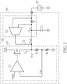
- FIG. 3 is a diagram illustrating a voltage regulator 300 according to one embodiment of the present invention.
- the voltage regulator 300 is within a package, and the voltage regulator 300 is configured to receive an input voltage VIN to provide a stable output voltage Vout to a device 302, and the device 302 draws an output current IL from the voltage regulator 300.
- the voltage regulator 300 comprises a voltage control circuit 310, a current control circuit 320 and an output capacitor CL, wherein the voltage control circuit 310 comprises an error amplifier 312, a current generator (a transistor M1 serves as the current generator) and two resistors R1 and R2, and the current control circuit 320 comprises a transconductance amplifier 322 and a resistor R.
- the voltage control circuit 310 is configured to provide a first current I1 to an output terminal Nout of the voltage regulator 300, the current control circuit 320 is configured to provide a second current 12 to the output terminal Nout, and the first current I1 and the second current 12 are combined to serve as the output current IL.
- the voltage control circuit 310 is configured to receive the output voltage Vout to generate the first current I1, so that the output voltage Vout maintains a constant voltage.
- the resistors R1 and R2 serve as a voltage divider to divides the output voltage Vout to generate a divided voltage Vdiv
- the error amplifier 312 compares the divided voltage Vdiv with a reference voltage VREF to generate a control signal to control the transistor M1 to provide the first current I1.
- the output current IL flows through the resistor R and forms a cross voltage
- the transconductance amplifier 322 converts a voltage difference between the terminals of the resistor R to generate the second current 12.
- the resistor R may be a parasitic resistor of a routing (e.g. PCB routing). In another embodiment, the resistor R may be intended position for the voltage regulator 300 (i.e., not parasitic resistor).
- the voltage regulator 300 has fast response when the output voltage Vout is away from the desired level.
- each of the voltage control circuit 310 and the current control circuit 320 has its own feedback loop, the second current 12 provided by the current control circuit 320 does not exceed the required output current IL, and the voltage control circuit 310 is configured to provide the first current I1 to supplement the insufficient current, so the loops of the voltage control circuit 310 and the current control circuit 320 do not conflict.
- the voltage control circuit 310 provides a portion of the output current IL, the voltage control circuit 310 with lower transient response does not need to provide large current to the output terminal Nout, therefore the voltage control circuit 310 has easier loop compensation design.
- the output capacitor CL can be designed smaller due to the design of the current control circuit 320, the output capacitor CL can be designed within the package without being positioned on a printed circuit board, therefore the manufacturing cost can be reduced.
- N is greater than M.
- a buffer can be positioned at an output terminal of the current control circuit 220 shown in FIG. 2 or the transconductance amplifier 322 shown in FIG. 3 .
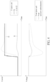
- FIG. 4 is a simulation result of the voltage regulator 100/200/300 according to one embodiment of the present invention.
- the current control circuit 120/220/320 can immediately provide the second current 12 to compensate the output voltage Vout, so that the output voltage Vout returns to the desired level in a short time.
- FIG. 4 also shows the conventional voltage regulator that does not include the current control circuit 120/220/320. Compared with the conventional voltage regulator, the embodiments shown in FIGs. 1 - 3 do have a faster response time.
Landscapes
- Engineering & Computer Science (AREA)
- Physics & Mathematics (AREA)
- Electromagnetism (AREA)
- General Physics & Mathematics (AREA)
- Radar, Positioning & Navigation (AREA)
- Automation & Control Theory (AREA)
- Power Engineering (AREA)
- Continuous-Control Power Sources That Use Transistors (AREA)
- Control Of Eletrric Generators (AREA)
- Oscillators With Electromechanical Resonators (AREA)
Abstract
Description
- This application claims the priority of
US Provisional Application No. 63/061,821 (filed on August 6th, 2020 - A voltage regulator is a system designed to automatically maintain a constant output voltage. In order to have the constant output voltage, an error amplifier designed in the voltage regulator is configured to compare output voltage with a reference voltage to generate a control signal to charge or discharge an output terminal. However, this control mechanism using the output voltage as a feedback signal has a slower response, that is the voltage regulator will charge or discharge the output terminal only after the voltage is away from the desired level for a period of time.
- In order to improve the transient response of the voltage regulator, the voltage regulator may be designed to have higher quiescent current or to have large output capacitor. However, higher quiescent current means higher power consumption; and designing large output capacitor will increase the manufacturing cost.
- It is therefore an objective of the present invention to providing a voltage regulator with hybrid control, which has fast transient response with lower manufacturing cost, to solve the above-mentioned problems.
- According to one embodiment of the present invention, a voltage regulator comprising a voltage control circuit and a current control circuit is disclosed. The voltage control circuit is configured to receive an output voltage of the voltage regulator to generate a first current to an output terminal of the voltage regulator; and the current control circuit is configured to generate a second current to the output terminal of the voltage regulator according to an output current of the voltage regulator, wherein the output current is generated according to the first current and the second current.
- These and other objectives of the present invention will no doubt become obvious to those of ordinary skill in the art after reading the following detailed description of the preferred embodiment that is illustrated in the various figures and drawings.
-
-
FIG. 1 is a diagram illustrating a voltage regulator according to one embodiment of the present invention. -
FIG. 2 is a diagram illustrating a voltage regulator according to another embodiment of the present invention. -
FIG. 3 is a diagram illustrating a voltage regulator according to another embodiment of the present invention. -
FIG. 4 is a simulation result of the voltage regulator according to one embodiment of the present invention. - Certain terms are used throughout the following description and claims to refer to particular system components. As one skilled in the art will appreciate, manufacturers may refer to a component by different names. This document does not intend to distinguish between components that differ in name but not function. In the following discussion and in the claims, the terms "including" and "comprising" are used in an open-ended fashion, and thus should be interpreted to mean "including, but not limited to ...". The terms "couple" and "couples" are intended to mean either an indirect or a direct electrical connection. Thus, if a first device couples to a second device, that connection may be through a direct electrical connection, or through an indirect electrical connection via other devices and connections.
-
FIG. 1 is a diagram illustrating avoltage regulator 100 according to one embodiment of the present invention. As shown inFIG. 1 , thevoltage regulator 100 is coupled to adevice 102, thevoltage regulator 100 is configured to provide a stable output voltage Vout to thedevice 102, and thedevice 102 draws an output current IL from thevoltage regulator 100. Thevoltage regulator 100 comprises avoltage control circuit 110, acurrent control circuit 120 and an output capacitor CL, wherein thevoltage control circuit 110 is configured to provide a first current I1 to an output terminal Nout of thevoltage regulator 100, thecurrent control circuit 120 is configured to provide asecond current 12 to the output terminal Nout, and the first current I1 and thesecond current 12 are combined to serve as the output current IL. - In this embodiment, the
voltage control circuit 110 is configured to receive the output voltage Vout to generate the first current I1, so that the output voltage Vout maintains a constant voltage. Specifically, if the output voltage Vout drops, thevoltage control circuit 110 can determine that the output voltage Vout is lower than a desired level, and thevoltage control circuit 110 outputs higher first current I1 to increase the output voltage Vout. If the output voltage Vout is above the desired level, thevoltage control circuit 110 outputs lower first current I1 to decrease the output voltage Vout. Thecurrent control circuit 120 is configured to receive the output current IL to generate thesecond current 12, so that thevoltage regulator 100 has a faster response when the output voltage Vout is away from the desired level. Specifically, if thedevice 102 draws more output current IL and the output voltage Vout drops, thecurrent control circuit 110 can immediately provide highersecond current 12 to increase the output voltage Vout. - In the embodiment shown in
FIG. 1 , by designing thecurrent control circuit 120 to use the output current IL to generate thesecond current 12, the output voltage Vout can be compensated to make the output voltage Vout return to the desired level in a short time. Therefore, thevoltage regulator 100 has fast response when the output voltage Vout is away from the desired level. In addition, each of thevoltage control circuit 110 and thecurrent control circuit 120 has its own feedback loop, thesecond current 12 provided by thecurrent control circuit 120 does not exceed the required output current IL, and thevoltage control circuit 110 is configured to provide the first current I1 to supplement the insufficient current, so the loops of thevoltage control circuit 110 and thecurrent control circuit 120 do not conflict. Furthermore, because thecurrent control circuit 120 provides a portion of the output current IL, thevoltage control circuit 110 with lower transient response does not need to provide large current to the output terminal Nout, and the output capacitor CL can be designed smaller, that is thevoltage control circuit 110 has easier loop compensation design and the manufacturing cost can be reduced. - In one embodiment, the second current 12 provided by the
current control circuit 120 has a fixed proportional relationship with the output current IL, that is I2=N*IL, wherein N can be any suitable value such as 80% or 90%. In addition, because the IL=I1+I2, the first current I1 provided by thevoltage control circuit 110 is also has a fixed proportional relationship with the output current IL, that is I1=M*IL, wherein M+N=100%. In one embodiment, in order to have fast transient response, N is greater than M, for example, N is equal to 90% while M is equal to 10%. -
FIG. 2 is a diagram illustrating avoltage regulator 200 according to one embodiment of the present invention. As shown inFIG. 2 , thevoltage regulator 200 is within a package, and thevoltage regulator 200 is configured to receive an input voltage VIN to provide a stable output voltage Vout to adevice 202 via the output capacitor CL and a resistor R, and thedevice 202 draws an output current IL from thevoltage regulator 200. Thevoltage regulator 200 comprises avoltage control circuit 210 and acurrent control circuit 220, wherein thevoltage control circuit 210 comprises anerror amplifier 212, a current generator (a transistor M1 serves as the current generator) and two resistors R1 and R2, and thecurrent control circuit 220 is implemented by a transconductance amplifier. Thevoltage control circuit 210 is configured to provide a first current I1 to an output terminal Nout of thevoltage regulator 200, thecurrent control circuit 220 is configured to provide asecond current 12 to the output terminal Nout, and the first current I1 and thesecond current 12 are combined to serve as the output current IL. - In this embodiment, the
voltage control circuit 210 is configured to receive the output voltage Vout to generate the first current I1, so that the output voltage Vout maintains a constant voltage. Specifically, the resistors R1 and R2 serve as a voltage divider to divides the output voltage Vout to generate a divided voltage Vdiv, theerror amplifier 212 compares the divided voltage Vdiv with a reference voltage VREF to generate a control signal to control the transistor M1 to provide the first current I1. In addition, the output current IL flows through the resistor R and forms a cross voltage, and thecurrent control circuit 220 receives the voltages at the terminals of the resistor R to generate the second current 12 (i.e., the transconductance amplifier converts a voltage difference between the terminals of the resistor R to generate the second current 12). - In one embodiment, the resistor R may be a parasitic resistor of a routing (e.g. PCB routing). In another embodiment, the resistor R may be intended position for the voltage regulator 200 (i.e., not parasitic resistor).
- In the embodiment shown in
FIG. 2 , by designing thecurrent control circuit 220 to use the output current IL to generate thesecond current 12, the output voltage Vout can be compensated to make the output voltage Vout return to the desired level in a short time. Therefore, thevoltage regulator 200 has fast response when the output voltage Vout is away from the desired level. In addition, each of thevoltage control circuit 210 and thecurrent control circuit 220 has its own feedback loop, thesecond current 12 provided by thecurrent control circuit 220 does not exceed the required output current IL, and thevoltage control circuit 210 is configured to provide the first current I1 to supplement the insufficient current, so the loops of thevoltage control circuit 210 and thecurrent control circuit 220 do not conflict. Furthermore, because thecurrent control circuit 220 provides a portion of the output current IL, thevoltage control circuit 210 with lower transient response does not need to provide large current to the output terminal Nout, and the output capacitor CL can be designed smaller, that is thevoltage control circuit 210 has easier loop compensation design and the manufacturing cost can be reduced. - In one embodiment, the second current 12 provided by the
current control circuit 220 has a fixed proportional relationship with the output current IL, that is I2=N*IL, wherein N can be any suitable value such as 80% or 90%. In addition, because the IL=I1+I2, the first current I1 provided by thevoltage control circuit 210 is also has a fixed proportional relationship with the output current IL, that is I1=M*IL, wherein M+N=100%. In one embodiment, in order to have fast transient response, N is greater than M. -
FIG. 3 is a diagram illustrating avoltage regulator 300 according to one embodiment of the present invention. As shown inFIG. 3 , thevoltage regulator 300 is within a package, and thevoltage regulator 300 is configured to receive an input voltage VIN to provide a stable output voltage Vout to adevice 302, and thedevice 302 draws an output current IL from thevoltage regulator 300. Thevoltage regulator 300 comprises avoltage control circuit 310, acurrent control circuit 320 and an output capacitor CL, wherein thevoltage control circuit 310 comprises anerror amplifier 312, a current generator (a transistor M1 serves as the current generator) and two resistors R1 and R2, and thecurrent control circuit 320 comprises atransconductance amplifier 322 and a resistor R. Thevoltage control circuit 310 is configured to provide a first current I1 to an output terminal Nout of thevoltage regulator 300, thecurrent control circuit 320 is configured to provide asecond current 12 to the output terminal Nout, and the first current I1 and thesecond current 12 are combined to serve as the output current IL. - In this embodiment, the
voltage control circuit 310 is configured to receive the output voltage Vout to generate the first current I1, so that the output voltage Vout maintains a constant voltage. Specifically, the resistors R1 and R2 serve as a voltage divider to divides the output voltage Vout to generate a divided voltage Vdiv, theerror amplifier 312 compares the divided voltage Vdiv with a reference voltage VREF to generate a control signal to control the transistor M1 to provide the first current I1. In addition, the output current IL flows through the resistor R and forms a cross voltage, and thetransconductance amplifier 322 converts a voltage difference between the terminals of the resistor R to generate thesecond current 12. - In one embodiment, the resistor R may be a parasitic resistor of a routing (e.g. PCB routing). In another embodiment, the resistor R may be intended position for the voltage regulator 300 (i.e., not parasitic resistor).
- In the embodiment shown in
FIG. 3 , by designing thecurrent control circuit 320 to use the output current IL to generate thesecond current 12, the output voltage Vout can be compensated to make the output voltage Vout return to the desired level in a short time. Therefore, thevoltage regulator 300 has fast response when the output voltage Vout is away from the desired level. In addition, each of thevoltage control circuit 310 and thecurrent control circuit 320 has its own feedback loop, the second current 12 provided by thecurrent control circuit 320 does not exceed the required output current IL, and thevoltage control circuit 310 is configured to provide the first current I1 to supplement the insufficient current, so the loops of thevoltage control circuit 310 and thecurrent control circuit 320 do not conflict. Furthermore, because thecurrent control circuit 320 provides a portion of the output current IL, thevoltage control circuit 310 with lower transient response does not need to provide large current to the output terminal Nout, therefore thevoltage control circuit 310 has easier loop compensation design. In addition, because the output capacitor CL can be designed smaller due to the design of thecurrent control circuit 320, the output capacitor CL can be designed within the package without being positioned on a printed circuit board, therefore the manufacturing cost can be reduced. - In one embodiment, the second current 12 provided by the
current control circuit 320 has a fixed proportional relationship with the output current IL, that is I2=N*IL, wherein N can be any suitable value such as 80% or 90%. In addition, because the IL=I1+I2, the first current I1 provided by thevoltage control circuit 310 is also has a fixed proportional relationship with the output current IL, that is I1=M*IL, wherein M+N=100%. In one embodiment, in order to have fast transient response, N is greater than M. - In another embodiment of the present invention, a buffer can be positioned at an output terminal of the
current control circuit 220 shown inFIG. 2 or thetransconductance amplifier 322 shown inFIG. 3 . -
FIG. 4 is a simulation result of thevoltage regulator 100/200/300 according to one embodiment of the present invention. As shown inFIG. 4 , when thedevice 102/202/302 suddenly draws a large amount of current, that is the output current IL increases rapidly, thecurrent control circuit 120/220/320 can immediately provide the second current 12 to compensate the output voltage Vout, so that the output voltage Vout returns to the desired level in a short time.FIG. 4 also shows the conventional voltage regulator that does not include thecurrent control circuit 120/220/320. Compared with the conventional voltage regulator, the embodiments shown inFIGs. 1 - 3 do have a faster response time. - Those skilled in the art will readily observe that numerous modifications and alterations of the device and method may be made while retaining the teachings of the invention. Accordingly, the above disclosure should be construed as limited only by the metes and bounds of the appended claims.
Claims (10)
- A voltage regulator (100, 200, 300), comprising:a voltage control circuit (110, 210, 310), configured to receive an output voltage of the voltage regulator (100, 200, 300) to generate a first current to an output terminal of the voltage regulator (100, 200, 300); anda current control circuit (120, 220, 320), configured to generate a second current to the output terminal of the voltage regulator (100, 200, 300) according to an output current of the voltage regulator (100, 200, 300), wherein the output current is generated according to the first current and the second current.
- The voltage regulator (100, 200, 300) of claim 1, wherein the second current has a fixed ratio to the output current.
- The voltage regulator (100, 200, 300) of claim 2, wherein the second current is equal to N times the output current, and the first second current is equal to M times the output current.
- The voltage regulator (100, 200, 300) of claim 3, wherein a summation of M and N is equal to 100%.
- The voltage regulator (100, 200, 300) of claim 3, wherein N is greater than M.
- The voltage regulator (100, 200, 300) of claim 1, wherein a loop of the voltage control circuit (110, 210, 310) and a loop of the current control circuit (120, 220, 320) are independent of each other.
- The voltage regulator (100, 200, 300) of claim 6, wherein the voltage control circuit (110, 210, 310) comprises:an error amplifier (212, 312), configured to compare a single derived from the output voltage with a reference voltage to generate a control signal; anda current generator (M1), configured to generate the first current according to the control signal.
- The voltage regulator (100, 200, 300) of claim 6, wherein the current control circuit (120, 220, 320) comprises a transconductance amplifier configured to receive a voltage signal generated according to the output current to generate the second current.
- The voltage regulator (100, 200, 300) of claim 6, wherein the current control circuit (120, 220, 320) comprises:a resistor (R1, R2), coupled to the output terminal of the voltage regulator (100, 200, 300), wherein the output current flows through the resistor (R1, R2); anda transconductance amplifier (332), configured to receive voltage signals at two terminals of the resistor (R1, R2) to generate the second current.
- The voltage regulator (100, 200, 300) of claim 9, further comprising:an output capacitor (CL), coupled between the output terminal of the voltage regulator (100, 200, 300) and a reference voltage;wherein the output capacitor (CL) and the voltage regulator (100, 200, 300) are within a single package.
Applications Claiming Priority (2)
| Application Number | Priority Date | Filing Date | Title |
|---|---|---|---|
| US202063061821P | 2020-08-06 | 2020-08-06 | |
| US17/368,853 US11791725B2 (en) | 2020-08-06 | 2021-07-07 | Voltage regulator with hybrid control for fast transient response |
Publications (2)
| Publication Number | Publication Date |
|---|---|
| EP3951550A1 true EP3951550A1 (en) | 2022-02-09 |
| EP3951550B1 EP3951550B1 (en) | 2023-10-04 |
Family
ID=77226607
Family Applications (1)
| Application Number | Title | Priority Date | Filing Date |
|---|---|---|---|
| EP21189705.3A Active EP3951550B1 (en) | 2020-08-06 | 2021-08-04 | Voltage regulator with hybrid control for fast transient response |
Country Status (4)
| Country | Link |
|---|---|
| US (1) | US11791725B2 (en) |
| EP (1) | EP3951550B1 (en) |
| CN (1) | CN114063692B (en) |
| TW (1) | TWI786741B (en) |
Families Citing this family (2)
| Publication number | Priority date | Publication date | Assignee | Title |
|---|---|---|---|---|
| US11960311B2 (en) | 2020-07-28 | 2024-04-16 | Medtronic Minimed, Inc. | Linear voltage regulator with isolated supply current |
| US12242291B2 (en) | 2022-09-16 | 2025-03-04 | Infineon Technologies Ag | Current controlled voltage regulator testing |
Citations (3)
| Publication number | Priority date | Publication date | Assignee | Title |
|---|---|---|---|---|
| US20120146597A1 (en) * | 2010-12-09 | 2012-06-14 | Advantest Corporation | Power supply apparatus |
| US20130234687A1 (en) * | 2012-03-08 | 2013-09-12 | Seiko Instruments Inc. | Voltage regulator |
| US9473027B2 (en) * | 2014-07-25 | 2016-10-18 | Monolithic Power Systems, Inc. | Voltage regulator with hybrid adaptive voltage position and control method thereof |
Family Cites Families (21)
| Publication number | Priority date | Publication date | Assignee | Title |
|---|---|---|---|---|
| US5747976A (en) | 1996-03-26 | 1998-05-05 | Raytheon Company | Constant on-time architecture for switching regulators |
| US5889392A (en) | 1997-03-06 | 1999-03-30 | Maxim Integrated Products, Inc. | Switch-mode regulators and methods providing transient response speed-up |
| EP0892332B1 (en) | 1997-07-14 | 2005-03-09 | STMicroelectronics S.r.l. | Low power consumption linear voltage regulator having a fast response with respect to the load transients |
| DE69732699D1 (en) | 1997-08-29 | 2005-04-14 | St Microelectronics Srl | Linear voltage regulator with low consumption and high supply voltage suppression |
| US7248531B2 (en) | 2005-08-03 | 2007-07-24 | Mosaid Technologies Incorporated | Voltage down converter for high speed memory |
| US8754622B2 (en) | 2009-10-30 | 2014-06-17 | Linear Technology Corporation | Voltage regulator compensating for voltage drop along conductors between regulator output and load |
| TWI503644B (en) | 2012-10-05 | 2015-10-11 | Faraday Tech Corp | Calibration circuit for a voltage regulator |
| KR20150031054A (en) * | 2013-09-13 | 2015-03-23 | 에스케이하이닉스 주식회사 | Constant voltage generating apparatus |
| US9405309B2 (en) | 2014-11-29 | 2016-08-02 | Infineon Technologies Ag | Dual mode low-dropout linear regulator |
| DE102015205359B4 (en) * | 2015-03-24 | 2018-01-25 | Dialog Semiconductor (Uk) Limited | RESTRAIN LIMIT FOR A LOW DROPOUT CONTROLLER IN A DROPOUT CONDITION |
| US10014772B2 (en) * | 2016-08-03 | 2018-07-03 | Nxp B.V. | Voltage regulator |
| US9791874B1 (en) * | 2016-11-04 | 2017-10-17 | Nxp B.V. | NMOS-based voltage regulator |
| EP3367202B1 (en) | 2017-02-27 | 2020-05-27 | ams International AG | Low-dropout regulator having sourcing and sinking capabilities |
| RU2764604C2 (en) | 2017-10-05 | 2022-01-18 | Филип Моррис Продактс С.А. | Electrically controlled aerosol-generating apparatus with continuous power supply adjustment |
| CN110058631B (en) | 2018-01-18 | 2022-07-29 | 恩智浦美国有限公司 | Voltage regulator with feed forward circuit |
| CN108710399B (en) | 2018-04-25 | 2019-10-22 | 电子科技大学 | A LDO Circuit with High Transient Response |
| US10541608B1 (en) * | 2018-06-29 | 2020-01-21 | Linear Technology Holding, LLC | Differential controller with regulators |
| CN110874110B (en) * | 2018-08-29 | 2021-05-18 | 华邦电子股份有限公司 | Voltage regulator and dynamic bleeder circuit |
| US12032399B2 (en) * | 2021-04-15 | 2024-07-09 | Samsung Electronics Co., Ltd. | Integrated circuit and electronic device including the same |
| US11720128B2 (en) * | 2021-06-29 | 2023-08-08 | Stmicroelectronics S.R.L. | Voltage regulator |
| US11594961B2 (en) * | 2021-07-19 | 2023-02-28 | Infineon Technologies Austria Ag | Power supply system and control in a dynamic load configuration |
-
2021
- 2021-07-07 US US17/368,853 patent/US11791725B2/en active Active
- 2021-07-22 TW TW110126987A patent/TWI786741B/en active
- 2021-07-23 CN CN202110839318.9A patent/CN114063692B/en active Active
- 2021-08-04 EP EP21189705.3A patent/EP3951550B1/en active Active
Patent Citations (3)
| Publication number | Priority date | Publication date | Assignee | Title |
|---|---|---|---|---|
| US20120146597A1 (en) * | 2010-12-09 | 2012-06-14 | Advantest Corporation | Power supply apparatus |
| US20130234687A1 (en) * | 2012-03-08 | 2013-09-12 | Seiko Instruments Inc. | Voltage regulator |
| US9473027B2 (en) * | 2014-07-25 | 2016-10-18 | Monolithic Power Systems, Inc. | Voltage regulator with hybrid adaptive voltage position and control method thereof |
Non-Patent Citations (2)
| Title |
|---|
| PETER HARRINGTON ET AL: "A low noise, high power efficiency supply regulator for near-field power delivery", ANALOG INTEGRATED CIRCUITS AND SIGNAL PROCESSING, KLUWER ACADEMIC PUBLISHERS, BO, vol. 66, no. 2, 8 August 2010 (2010-08-08), pages 177 - 187, XP019879654, ISSN: 1573-1979, DOI: 10.1007/S10470-010-9511-7 * |
| SHIRMOHAMMADLI VAHIDEH ET AL: "An efficient CMOS LDO-assisted DC/DC buck regulator", 2016 CONFERENCE ON DESIGN OF CIRCUITS AND INTEGRATED SYSTEMS (DCIS), 1 November 2016 (2016-11-01), pages 1 - 4, XP055869706, ISBN: 978-1-5090-4565-5, Retrieved from the Internet <URL:https://upcommons.upc.edu/bitstream/2117/116204/1/3A_4.pdf> DOI: 10.1109/DCIS.2016.7845356 * |
Also Published As
| Publication number | Publication date |
|---|---|
| US20220045606A1 (en) | 2022-02-10 |
| CN114063692A (en) | 2022-02-18 |
| US11791725B2 (en) | 2023-10-17 |
| CN114063692B (en) | 2023-08-25 |
| TWI786741B (en) | 2022-12-11 |
| EP3951550B1 (en) | 2023-10-04 |
| TW202206961A (en) | 2022-02-16 |
Similar Documents
| Publication | Publication Date | Title |
|---|---|---|
| EP1378808B1 (en) | LDO regulator with wide output load range and fast internal loop | |
| US7893671B2 (en) | Regulator with improved load regulation | |
| KR100967261B1 (en) | Voltage regulator | |
| CN1661509A (en) | Efficient frequency compensation for linear voltage regulators | |
| EP2328056B1 (en) | Low-dropout linear regulator (LDO), method for providing an LDO and method for operating an LDO | |
| US7863873B2 (en) | Power management circuit and method of frequency compensation thereof | |
| US8878510B2 (en) | Reducing power consumption in a voltage regulator | |
| US9891643B2 (en) | Circuit to improve load transient behavior of voltage regulators and load switches | |
| US20040120169A1 (en) | Hysteretic DC-DC converters | |
| JP2005276190A (en) | Low dropout voltage regulator | |
| US11791725B2 (en) | Voltage regulator with hybrid control for fast transient response | |
| CN111596715B (en) | Voltage adjusting device, chip, power supply and electronic equipment | |
| US20080218133A1 (en) | Signal generating apparatus and method thereof | |
| US20140176096A1 (en) | Semiconductor device and power supply system including the same | |
| US6850118B2 (en) | Amplifier circuit and power supply provided therewith | |
| US8253401B2 (en) | Voltage conversion apparatus | |
| CN112363558A (en) | Voltage regulating circuit | |
| KR20110131113A (en) | Voltage Regulator | |
| US6812778B1 (en) | Compensating capacitive multiplier | |
| US7282902B2 (en) | Voltage regulator apparatus | |
| US7007178B2 (en) | Voltage adaptor card for motherboard | |
| TWI833291B (en) | Voltage regulating circuit | |
| US11695332B2 (en) | Voltage regulator for series-connected loads | |
| KR20160012858A (en) | Low dropout regulator | |
| US10663997B2 (en) | Electronic device circuit board |
Legal Events
| Date | Code | Title | Description |
|---|---|---|---|
| PUAI | Public reference made under article 153(3) epc to a published international application that has entered the european phase |
Free format text: ORIGINAL CODE: 0009012 |
|
| STAA | Information on the status of an ep patent application or granted ep patent |
Free format text: STATUS: THE APPLICATION HAS BEEN PUBLISHED |
|
| AK | Designated contracting states |
Kind code of ref document: A1 Designated state(s): AL AT BE BG CH CY CZ DE DK EE ES FI FR GB GR HR HU IE IS IT LI LT LU LV MC MK MT NL NO PL PT RO RS SE SI SK SM TR |
|
| STAA | Information on the status of an ep patent application or granted ep patent |
Free format text: STATUS: REQUEST FOR EXAMINATION WAS MADE |
|
| 17P | Request for examination filed |
Effective date: 20220808 |
|
| RBV | Designated contracting states (corrected) |
Designated state(s): AL AT BE BG CH CY CZ DE DK EE ES FI FR GB GR HR HU IE IS IT LI LT LU LV MC MK MT NL NO PL PT RO RS SE SI SK SM TR |
|
| GRAP | Despatch of communication of intention to grant a patent |
Free format text: ORIGINAL CODE: EPIDOSNIGR1 |
|
| STAA | Information on the status of an ep patent application or granted ep patent |
Free format text: STATUS: GRANT OF PATENT IS INTENDED |
|
| INTG | Intention to grant announced |
Effective date: 20230421 |
|
| P01 | Opt-out of the competence of the unified patent court (upc) registered |
Effective date: 20230607 |
|
| GRAS | Grant fee paid |
Free format text: ORIGINAL CODE: EPIDOSNIGR3 |
|
| GRAA | (expected) grant |
Free format text: ORIGINAL CODE: 0009210 |
|
| STAA | Information on the status of an ep patent application or granted ep patent |
Free format text: STATUS: THE PATENT HAS BEEN GRANTED |
|
| AK | Designated contracting states |
Kind code of ref document: B1 Designated state(s): AL AT BE BG CH CY CZ DE DK EE ES FI FR GB GR HR HU IE IS IT LI LT LU LV MC MK MT NL NO PL PT RO RS SE SI SK SM TR |
|
| REG | Reference to a national code |
Ref country code: GB Ref legal event code: FG4D |
|
| REG | Reference to a national code |
Ref country code: CH Ref legal event code: EP |
|
| REG | Reference to a national code |
Ref country code: IE Ref legal event code: FG4D |
|
| REG | Reference to a national code |
Ref country code: DE Ref legal event code: R096 Ref document number: 602021005574 Country of ref document: DE |
|
| REG | Reference to a national code |
Ref country code: LT Ref legal event code: MG9D |
|
| REG | Reference to a national code |
Ref country code: NL Ref legal event code: MP Effective date: 20231004 |
|
| REG | Reference to a national code |
Ref country code: AT Ref legal event code: MK05 Ref document number: 1618383 Country of ref document: AT Kind code of ref document: T Effective date: 20231004 |
|
| PG25 | Lapsed in a contracting state [announced via postgrant information from national office to epo] |
Ref country code: NL Free format text: LAPSE BECAUSE OF FAILURE TO SUBMIT A TRANSLATION OF THE DESCRIPTION OR TO PAY THE FEE WITHIN THE PRESCRIBED TIME-LIMIT Effective date: 20231004 |
|
| PG25 | Lapsed in a contracting state [announced via postgrant information from national office to epo] |
Ref country code: GR Free format text: LAPSE BECAUSE OF FAILURE TO SUBMIT A TRANSLATION OF THE DESCRIPTION OR TO PAY THE FEE WITHIN THE PRESCRIBED TIME-LIMIT Effective date: 20240105 |
|
| PG25 | Lapsed in a contracting state [announced via postgrant information from national office to epo] |
Ref country code: IS Free format text: LAPSE BECAUSE OF FAILURE TO SUBMIT A TRANSLATION OF THE DESCRIPTION OR TO PAY THE FEE WITHIN THE PRESCRIBED TIME-LIMIT Effective date: 20240204 |
|
| PG25 | Lapsed in a contracting state [announced via postgrant information from national office to epo] |
Ref country code: LT Free format text: LAPSE BECAUSE OF FAILURE TO SUBMIT A TRANSLATION OF THE DESCRIPTION OR TO PAY THE FEE WITHIN THE PRESCRIBED TIME-LIMIT Effective date: 20231004 |
|
| PG25 | Lapsed in a contracting state [announced via postgrant information from national office to epo] |
Ref country code: AT Free format text: LAPSE BECAUSE OF FAILURE TO SUBMIT A TRANSLATION OF THE DESCRIPTION OR TO PAY THE FEE WITHIN THE PRESCRIBED TIME-LIMIT Effective date: 20231004 |
|
| PG25 | Lapsed in a contracting state [announced via postgrant information from national office to epo] |
Ref country code: ES Free format text: LAPSE BECAUSE OF FAILURE TO SUBMIT A TRANSLATION OF THE DESCRIPTION OR TO PAY THE FEE WITHIN THE PRESCRIBED TIME-LIMIT Effective date: 20231004 |
|
| PG25 | Lapsed in a contracting state [announced via postgrant information from national office to epo] |
Ref country code: LT Free format text: LAPSE BECAUSE OF FAILURE TO SUBMIT A TRANSLATION OF THE DESCRIPTION OR TO PAY THE FEE WITHIN THE PRESCRIBED TIME-LIMIT Effective date: 20231004 Ref country code: IS Free format text: LAPSE BECAUSE OF FAILURE TO SUBMIT A TRANSLATION OF THE DESCRIPTION OR TO PAY THE FEE WITHIN THE PRESCRIBED TIME-LIMIT Effective date: 20240204 Ref country code: GR Free format text: LAPSE BECAUSE OF FAILURE TO SUBMIT A TRANSLATION OF THE DESCRIPTION OR TO PAY THE FEE WITHIN THE PRESCRIBED TIME-LIMIT Effective date: 20240105 Ref country code: ES Free format text: LAPSE BECAUSE OF FAILURE TO SUBMIT A TRANSLATION OF THE DESCRIPTION OR TO PAY THE FEE WITHIN THE PRESCRIBED TIME-LIMIT Effective date: 20231004 Ref country code: BG Free format text: LAPSE BECAUSE OF FAILURE TO SUBMIT A TRANSLATION OF THE DESCRIPTION OR TO PAY THE FEE WITHIN THE PRESCRIBED TIME-LIMIT Effective date: 20240104 Ref country code: AT Free format text: LAPSE BECAUSE OF FAILURE TO SUBMIT A TRANSLATION OF THE DESCRIPTION OR TO PAY THE FEE WITHIN THE PRESCRIBED TIME-LIMIT Effective date: 20231004 Ref country code: PT Free format text: LAPSE BECAUSE OF FAILURE TO SUBMIT A TRANSLATION OF THE DESCRIPTION OR TO PAY THE FEE WITHIN THE PRESCRIBED TIME-LIMIT Effective date: 20240205 |
|
| PG25 | Lapsed in a contracting state [announced via postgrant information from national office to epo] |
Ref country code: SE Free format text: LAPSE BECAUSE OF FAILURE TO SUBMIT A TRANSLATION OF THE DESCRIPTION OR TO PAY THE FEE WITHIN THE PRESCRIBED TIME-LIMIT Effective date: 20231004 Ref country code: RS Free format text: LAPSE BECAUSE OF FAILURE TO SUBMIT A TRANSLATION OF THE DESCRIPTION OR TO PAY THE FEE WITHIN THE PRESCRIBED TIME-LIMIT Effective date: 20231004 Ref country code: PL Free format text: LAPSE BECAUSE OF FAILURE TO SUBMIT A TRANSLATION OF THE DESCRIPTION OR TO PAY THE FEE WITHIN THE PRESCRIBED TIME-LIMIT Effective date: 20231004 Ref country code: NO Free format text: LAPSE BECAUSE OF FAILURE TO SUBMIT A TRANSLATION OF THE DESCRIPTION OR TO PAY THE FEE WITHIN THE PRESCRIBED TIME-LIMIT Effective date: 20240104 Ref country code: LV Free format text: LAPSE BECAUSE OF FAILURE TO SUBMIT A TRANSLATION OF THE DESCRIPTION OR TO PAY THE FEE WITHIN THE PRESCRIBED TIME-LIMIT Effective date: 20231004 Ref country code: HR Free format text: LAPSE BECAUSE OF FAILURE TO SUBMIT A TRANSLATION OF THE DESCRIPTION OR TO PAY THE FEE WITHIN THE PRESCRIBED TIME-LIMIT Effective date: 20231004 |
|
| REG | Reference to a national code |
Ref country code: DE Ref legal event code: R097 Ref document number: 602021005574 Country of ref document: DE |
|
| PG25 | Lapsed in a contracting state [announced via postgrant information from national office to epo] |
Ref country code: DK Free format text: LAPSE BECAUSE OF FAILURE TO SUBMIT A TRANSLATION OF THE DESCRIPTION OR TO PAY THE FEE WITHIN THE PRESCRIBED TIME-LIMIT Effective date: 20231004 |
|
| PG25 | Lapsed in a contracting state [announced via postgrant information from national office to epo] |
Ref country code: CZ Free format text: LAPSE BECAUSE OF FAILURE TO SUBMIT A TRANSLATION OF THE DESCRIPTION OR TO PAY THE FEE WITHIN THE PRESCRIBED TIME-LIMIT Effective date: 20231004 |
|
| PG25 | Lapsed in a contracting state [announced via postgrant information from national office to epo] |
Ref country code: SK Free format text: LAPSE BECAUSE OF FAILURE TO SUBMIT A TRANSLATION OF THE DESCRIPTION OR TO PAY THE FEE WITHIN THE PRESCRIBED TIME-LIMIT Effective date: 20231004 |
|
| PG25 | Lapsed in a contracting state [announced via postgrant information from national office to epo] |
Ref country code: SM Free format text: LAPSE BECAUSE OF FAILURE TO SUBMIT A TRANSLATION OF THE DESCRIPTION OR TO PAY THE FEE WITHIN THE PRESCRIBED TIME-LIMIT Effective date: 20231004 Ref country code: SK Free format text: LAPSE BECAUSE OF FAILURE TO SUBMIT A TRANSLATION OF THE DESCRIPTION OR TO PAY THE FEE WITHIN THE PRESCRIBED TIME-LIMIT Effective date: 20231004 Ref country code: RO Free format text: LAPSE BECAUSE OF FAILURE TO SUBMIT A TRANSLATION OF THE DESCRIPTION OR TO PAY THE FEE WITHIN THE PRESCRIBED TIME-LIMIT Effective date: 20231004 Ref country code: IT Free format text: LAPSE BECAUSE OF FAILURE TO SUBMIT A TRANSLATION OF THE DESCRIPTION OR TO PAY THE FEE WITHIN THE PRESCRIBED TIME-LIMIT Effective date: 20231004 Ref country code: EE Free format text: LAPSE BECAUSE OF FAILURE TO SUBMIT A TRANSLATION OF THE DESCRIPTION OR TO PAY THE FEE WITHIN THE PRESCRIBED TIME-LIMIT Effective date: 20231004 Ref country code: DK Free format text: LAPSE BECAUSE OF FAILURE TO SUBMIT A TRANSLATION OF THE DESCRIPTION OR TO PAY THE FEE WITHIN THE PRESCRIBED TIME-LIMIT Effective date: 20231004 Ref country code: CZ Free format text: LAPSE BECAUSE OF FAILURE TO SUBMIT A TRANSLATION OF THE DESCRIPTION OR TO PAY THE FEE WITHIN THE PRESCRIBED TIME-LIMIT Effective date: 20231004 |
|
| PLBE | No opposition filed within time limit |
Free format text: ORIGINAL CODE: 0009261 |
|
| STAA | Information on the status of an ep patent application or granted ep patent |
Free format text: STATUS: NO OPPOSITION FILED WITHIN TIME LIMIT |
|
| 26N | No opposition filed |
Effective date: 20240705 |
|
| PG25 | Lapsed in a contracting state [announced via postgrant information from national office to epo] |
Ref country code: SI Free format text: LAPSE BECAUSE OF FAILURE TO SUBMIT A TRANSLATION OF THE DESCRIPTION OR TO PAY THE FEE WITHIN THE PRESCRIBED TIME-LIMIT Effective date: 20231004 |
|
| PG25 | Lapsed in a contracting state [announced via postgrant information from national office to epo] |
Ref country code: SI Free format text: LAPSE BECAUSE OF FAILURE TO SUBMIT A TRANSLATION OF THE DESCRIPTION OR TO PAY THE FEE WITHIN THE PRESCRIBED TIME-LIMIT Effective date: 20231004 |
|
| REG | Reference to a national code |
Ref country code: CH Ref legal event code: PL |
|
| PG25 | Lapsed in a contracting state [announced via postgrant information from national office to epo] |
Ref country code: LU Free format text: LAPSE BECAUSE OF NON-PAYMENT OF DUE FEES Effective date: 20240804 |
|
| PG25 | Lapsed in a contracting state [announced via postgrant information from national office to epo] |
Ref country code: CH Free format text: LAPSE BECAUSE OF NON-PAYMENT OF DUE FEES Effective date: 20240831 Ref country code: MC Free format text: LAPSE BECAUSE OF FAILURE TO SUBMIT A TRANSLATION OF THE DESCRIPTION OR TO PAY THE FEE WITHIN THE PRESCRIBED TIME-LIMIT Effective date: 20231004 |
|
| REG | Reference to a national code |
Ref country code: BE Ref legal event code: MM Effective date: 20240831 |
|
| PGFP | Annual fee paid to national office [announced via postgrant information from national office to epo] |
Ref country code: GB Payment date: 20250612 Year of fee payment: 5 |
|
| PG25 | Lapsed in a contracting state [announced via postgrant information from national office to epo] |
Ref country code: BE Free format text: LAPSE BECAUSE OF NON-PAYMENT OF DUE FEES Effective date: 20240831 |
|
| PGFP | Annual fee paid to national office [announced via postgrant information from national office to epo] |
Ref country code: FR Payment date: 20250610 Year of fee payment: 5 |
|
| PG25 | Lapsed in a contracting state [announced via postgrant information from national office to epo] |
Ref country code: IE Free format text: LAPSE BECAUSE OF NON-PAYMENT OF DUE FEES Effective date: 20240804 |
|
| PG25 | Lapsed in a contracting state [announced via postgrant information from national office to epo] |
Ref country code: FI Free format text: LAPSE BECAUSE OF FAILURE TO SUBMIT A TRANSLATION OF THE DESCRIPTION OR TO PAY THE FEE WITHIN THE PRESCRIBED TIME-LIMIT Effective date: 20231004 |
|
| PGFP | Annual fee paid to national office [announced via postgrant information from national office to epo] |
Ref country code: DE Payment date: 20250611 Year of fee payment: 5 |
|
| PG25 | Lapsed in a contracting state [announced via postgrant information from national office to epo] |
Ref country code: CY Free format text: LAPSE BECAUSE OF FAILURE TO SUBMIT A TRANSLATION OF THE DESCRIPTION OR TO PAY THE FEE WITHIN THE PRESCRIBED TIME-LIMIT; INVALID AB INITIO Effective date: 20210804 |
|
| PG25 | Lapsed in a contracting state [announced via postgrant information from national office to epo] |
Ref country code: HU Free format text: LAPSE BECAUSE OF FAILURE TO SUBMIT A TRANSLATION OF THE DESCRIPTION OR TO PAY THE FEE WITHIN THE PRESCRIBED TIME-LIMIT; INVALID AB INITIO Effective date: 20210804 |