EP3948308B1 - Partial insulation with diagnostic pickup coils - Google Patents
Partial insulation with diagnostic pickup coils Download PDFInfo
- Publication number
- EP3948308B1 EP3948308B1 EP20717131.5A EP20717131A EP3948308B1 EP 3948308 B1 EP3948308 B1 EP 3948308B1 EP 20717131 A EP20717131 A EP 20717131A EP 3948308 B1 EP3948308 B1 EP 3948308B1
- Authority
- EP
- European Patent Office
- Prior art keywords
- hts
- insulating layer
- track
- pickup
- partially insulating
- Prior art date
- Legal status (The legal status is an assumption and is not a legal conclusion. Google has not performed a legal analysis and makes no representation as to the accuracy of the status listed.)
- Active
Links
Images


Classifications
-
- H—ELECTRICITY
- H01—ELECTRIC ELEMENTS
- H01F—MAGNETS; INDUCTANCES; TRANSFORMERS; SELECTION OF MATERIALS FOR THEIR MAGNETIC PROPERTIES
- H01F6/00—Superconducting magnets; Superconducting coils
- H01F6/06—Coils, e.g. winding, insulating, terminating or casing arrangements therefor
-
- A—HUMAN NECESSITIES
- A61—MEDICAL OR VETERINARY SCIENCE; HYGIENE
- A61N—ELECTROTHERAPY; MAGNETOTHERAPY; RADIATION THERAPY; ULTRASOUND THERAPY
- A61N5/00—Radiation therapy
- A61N5/10—X-ray therapy; Gamma-ray therapy; Particle-irradiation therapy
- A61N5/1077—Beam delivery systems
-
- G—PHYSICS
- G21—NUCLEAR PHYSICS; NUCLEAR ENGINEERING
- G21K—HANDLING OF PARTICLES OR IONISING RADIATION NOT OTHERWISE PROVIDED FOR; IRRADIATION DEVICES; GAMMA RAY OR X-RAY MICROSCOPES
- G21K1/00—Arrangements for handling particles or ionising radiation, e.g. focusing or moderating
- G21K1/08—Deviation, concentration or focusing of the beam by electric or magnetic means
- G21K1/093—Deviation, concentration or focusing of the beam by electric or magnetic means by magnetic means
-
- G—PHYSICS
- G21—NUCLEAR PHYSICS; NUCLEAR ENGINEERING
- G21K—HANDLING OF PARTICLES OR IONISING RADIATION NOT OTHERWISE PROVIDED FOR; IRRADIATION DEVICES; GAMMA RAY OR X-RAY MICROSCOPES
- G21K5/00—Irradiation devices
- G21K5/04—Irradiation devices with beam-forming means
-
- H—ELECTRICITY
- H01—ELECTRIC ELEMENTS
- H01F—MAGNETS; INDUCTANCES; TRANSFORMERS; SELECTION OF MATERIALS FOR THEIR MAGNETIC PROPERTIES
- H01F6/00—Superconducting magnets; Superconducting coils
- H01F6/02—Quenching; Protection arrangements during quenching
-
- H—ELECTRICITY
- H05—ELECTRIC TECHNIQUES NOT OTHERWISE PROVIDED FOR
- H05H—PLASMA TECHNIQUE; PRODUCTION OF ACCELERATED ELECTRICALLY-CHARGED PARTICLES OR OF NEUTRONS; PRODUCTION OR ACCELERATION OF NEUTRAL MOLECULAR OR ATOMIC BEAMS
- H05H7/00—Details of devices of the types covered by groups H05H9/00, H05H11/00, H05H13/00
- H05H7/04—Magnet systems, e.g. undulators, wigglers; Energisation thereof
-
- H—ELECTRICITY
- H05—ELECTRIC TECHNIQUES NOT OTHERWISE PROVIDED FOR
- H05K—PRINTED CIRCUITS; CASINGS OR CONSTRUCTIONAL DETAILS OF ELECTRIC APPARATUS; MANUFACTURE OF ASSEMBLAGES OF ELECTRICAL COMPONENTS
- H05K1/00—Printed circuits
- H05K1/16—Printed circuits incorporating printed electric components, e.g. printed resistors, capacitors or inductors
- H05K1/165—Printed circuits incorporating printed electric components, e.g. printed resistors, capacitors or inductors incorporating printed inductors
-
- H—ELECTRICITY
- H05—ELECTRIC TECHNIQUES NOT OTHERWISE PROVIDED FOR
- H05K—PRINTED CIRCUITS; CASINGS OR CONSTRUCTIONAL DETAILS OF ELECTRIC APPARATUS; MANUFACTURE OF ASSEMBLAGES OF ELECTRICAL COMPONENTS
- H05K3/00—Apparatus or processes for manufacturing printed circuits
- H05K3/40—Forming printed elements for providing electric connections to or between printed circuits
- H05K3/42—Plated through-holes or plated via connections
- H05K3/429—Plated through-holes specially for multilayer circuits, e.g. having connections to inner circuit layers
-
- A—HUMAN NECESSITIES
- A61—MEDICAL OR VETERINARY SCIENCE; HYGIENE
- A61N—ELECTROTHERAPY; MAGNETOTHERAPY; RADIATION THERAPY; ULTRASOUND THERAPY
- A61N5/00—Radiation therapy
- A61N5/10—X-ray therapy; Gamma-ray therapy; Particle-irradiation therapy
- A61N2005/1085—X-ray therapy; Gamma-ray therapy; Particle-irradiation therapy characterised by the type of particles applied to the patient
- A61N2005/1087—Ions; Protons
-
- H—ELECTRICITY
- H05—ELECTRIC TECHNIQUES NOT OTHERWISE PROVIDED FOR
- H05H—PLASMA TECHNIQUE; PRODUCTION OF ACCELERATED ELECTRICALLY-CHARGED PARTICLES OR OF NEUTRONS; PRODUCTION OR ACCELERATION OF NEUTRAL MOLECULAR OR ATOMIC BEAMS
- H05H2277/00—Applications of particle accelerators
- H05H2277/10—Medical devices
- H05H2277/11—Radiotherapy
-
- H—ELECTRICITY
- H05—ELECTRIC TECHNIQUES NOT OTHERWISE PROVIDED FOR
- H05K—PRINTED CIRCUITS; CASINGS OR CONSTRUCTIONAL DETAILS OF ELECTRIC APPARATUS; MANUFACTURE OF ASSEMBLAGES OF ELECTRICAL COMPONENTS
- H05K2201/00—Indexing scheme relating to printed circuits covered by H05K1/00
- H05K2201/09—Shape and layout
- H05K2201/09209—Shape and layout details of conductors
- H05K2201/09654—Shape and layout details of conductors covering at least two types of conductors provided for in H05K2201/09218 - H05K2201/095
- H05K2201/09672—Superposed layout, i.e. in different planes
-
- H—ELECTRICITY
- H05—ELECTRIC TECHNIQUES NOT OTHERWISE PROVIDED FOR
- H05K—PRINTED CIRCUITS; CASINGS OR CONSTRUCTIONAL DETAILS OF ELECTRIC APPARATUS; MANUFACTURE OF ASSEMBLAGES OF ELECTRICAL COMPONENTS
- H05K2201/00—Indexing scheme relating to printed circuits covered by H05K1/00
- H05K2201/10—Details of components or other objects attached to or integrated in a printed circuit board
- H05K2201/10007—Types of components
- H05K2201/10151—Sensor
-
- Y—GENERAL TAGGING OF NEW TECHNOLOGICAL DEVELOPMENTS; GENERAL TAGGING OF CROSS-SECTIONAL TECHNOLOGIES SPANNING OVER SEVERAL SECTIONS OF THE IPC; TECHNICAL SUBJECTS COVERED BY FORMER USPC CROSS-REFERENCE ART COLLECTIONS [XRACs] AND DIGESTS
- Y02—TECHNOLOGIES OR APPLICATIONS FOR MITIGATION OR ADAPTATION AGAINST CLIMATE CHANGE
- Y02E—REDUCTION OF GREENHOUSE GAS [GHG] EMISSIONS, RELATED TO ENERGY GENERATION, TRANSMISSION OR DISTRIBUTION
- Y02E30/00—Energy generation of nuclear origin
- Y02E30/10—Nuclear fusion reactors
Definitions
- the present invention relates to high temperature superconducting (HTS) magnets.
- the invention relates to a partially insulating layer for use in a partially insulated HTS magnet.
- High temperature superconductors HTS
- low temperature superconductors LTS materials
- BCS theory All low temperature superconductors have a critical temperature (the temperature above which the material cannot be superconducting even in zero magnetic field) below about 30K.
- critical temperature the temperature above which the material cannot be superconducting even in zero magnetic field
- BCS theory The behaviour of HTS material is not described by BCS theory, and such materials may have critical temperatures above about 30K (though it should be noted that it is the physical differences in composition and superconducting operation, rather than the critical temperature, which define HTS and LTS material).
- HTS cuprate superconductors
- cuprate superconductors ceramics based on cuprates (compounds containing a copper oxide group), such as BSCCO, or ReBCO (where Re is a rare earth element, commonly Y or Gd).
- BSCCO or ReBCO
- Re is a rare earth element, commonly Y or Gd.
- Other HTS materials include iron pnictides (e.g. FeAs and FeSe) and magnesium diborate (MgB 2 ).
- ReBCO is typically manufactured as tapes, with a structure as shown in Figure 1 .
- Such tape 100 is generally approximately 100 ⁇ m thick, and includes a substrate 101 (typically electropolished hastelloy approximately 50 ⁇ m thick), on which is deposited by IBAD, magnetron sputtering, or another suitable technique a series of buffer layers known as the buffer stack 102, of approximate thickness 0.2 ⁇ m
- An epitaxial ReBCO-HTS layer 103 (deposited by MOCVD or another suitable technique) overlays the buffer stack, and is typically 1 ⁇ m thick.
- a 1-2 ⁇ m silver layer 104 is deposited on the HTS layer by sputtering or another suitable technique, and a copper stabilizer layer 105 is deposited on the tape by electroplating or another suitable technique, which often completely encapsulates the tape.
- the substrate 101 provides a mechanical backbone that can be fed through the manufacturing line and permit growth of subsequent layers.
- the buffer stack 102 is required to provide a biaxially textured crystalline template upon which to grow the HTS layer, and prevents chemical diffusion of elements from the substrate to the HTS which damage its superconducting properties.
- the silver layer 104 is required to provide a low resistance interface from the ReBCO to the stabiliser layer, and the stabiliser layer 105 provides an alternative current path in the event that any part of the ReBCO ceases superconducting (enters the "normal" state).
- exfoliated HTS tape can be manufactured, which lacks a substrate and buffer stack, and instead has silver layers on both sides of the HTS layer. Tape which has a substrate will be referred to as "substrated" HTS tape.
- HTS tapes may be arranged into HTS cables.
- An HTS cable comprises one or more HTS tapes, which are connected along their length by conductive material (normally copper).
- the HTS tapes may be stacked (i.e. arranged such that the HTS layers are parallel), or they may have some other arrangement of tapes, which may vary along the length of the cable.
- Notable special cases of HTS cables are single HTS tapes, and HTS pairs.
- HTS pairs comprise a pair of HTS tapes, arranged such that the HTS layers are parallel. Where substrated tape is used, HTS pairs may be type-0 (with the HTS layers facing each other), type-1 (with the HTS layer of one tape facing the substrate of the other), or type-2 (with the substrates facing each other).
- HTS cables comprising more than 2 tapes may arrange some or all of the tapes in HTS pairs.
- Stacked HTS tapes may comprise various arrangements of HTS pairs, most commonly either a stack of type-1 pairs or a stack of type-0 pairs and (or, equivalently, type-2 pairs).
- HTS cables may comprise a mix of substrated and exfoliated tape.
- a superconducting magnet is formed by arranging HTS cables (or individual HTS tapes, which for the purpose of this description can be treated as a single-tape cable) into coils, either by winding the HTS cables or by providing sections of the coil made from HTS cables and joining them together.
- HTS coils come in three broad classes:
- Non-insulated coils could also be considered as the low-resistance case of partially insulated coils.
- the insulation can comprise another conductor for quench detection as is disclosed in " Fundamental Evaluations of Applicability of LTS Quench Detectors to REBCO Pancake Coil" by HASEGAWA SHIN ET AL (doi:10.1109/TASC.2019.2900633 ).
- Having no or partial insulation between turns slows the rate at which the temperature of a local "hotspot" (normal zone) rises.
- the rate of growth (spatial propagation) of a normal (resistive HTS) zone in an HTS magnet depends on many parameters, but is typically less than 100 mm/s in the axial direction (ie: along the cable), and roughly 2-100 times slower in the transverse direction (ie: between adjacent turns).
- the exact rate of propagation of the normal zone in each direction depends on the thermal and electrical properties of the materials and cable construction utilised. In particular, the rate of transverse propagation is affected by the thermal properties of the material between turns.
- the transverse propagation can cause the entire cross section of the coil to become normal in a zone covering a small fraction of the coil's periphery, resulting in the total current of all turns flowing only in the metal stabilizer within the normal section. Outside the normal zone the conductors are still superconducting. The resistance of this normal zone is not enough to cause the magnet's current to fall quickly but results in the stored magnetic energy of the whole magnet being dumped into this small normal (resistive) volume, which is only growing around the coil periphery slowly. Unless this situation is detected quickly so that the magnet's stored energy can be dumped into a resistance external to the coil, the temperature of the normal zone will rise very quickly, which is likely to cause significant damage to conductors within the normal zone.
- HTS magnets are used in tokamak fusion reactors and plasma chambers, particularly in spherical tokamaks.
- a tokamak has two sets of magnets - poloidal field coils, which are aligned to produce a poloidal field and are generally circular, and toroidal field coils, which comprise a central column and a plurality of return limbs, and are arranged to produce a toroidal field.
- HTS magnets can be used for either set of field coils, but are particularly useful for toroidal field coils in small tokamaks, as such field coils have tight space limitations which the improved current density and/or reduced cooling requirements of HTS can help with significantly.
- Proton beam therapy is a type of particle therapy used in the treatment of cancers (and other conditions which respond to radiotherapy).
- PBT proton beam therapy
- a beam of protons is directed towards the treatment location (e.g. the tumour).
- PBCT proton boron capture therapy
- boron-11 is introduced to the target location, and a proton beam is used to initiate the p+ 11 B ⁇ 3 ⁇ reaction.
- the same apparatus can be used to provide proton beams for either PBT or PBCT.
- the proton beams for PBT and PBCT are generated by particle accelerators such as a cyclotrons or linear accelerators. Accelerators typically used for PBT and PBCT typically produce protons with energies in the range of 60 to 250MeV, with the most powerful currently operating facility having a maximum energy of 400 MeV.
- HTS magnets may be used within the accelerator, quadrupole magnets of the steering magnets, or dipole magnets of the steering magnets.
- a partially insulating layer for use in ar HTS magnet coil.
- the partially insulating layer comprises an insulating body 401 having within it a set of linking tracks and a set of pickup tracks.
- Each linking track is electrically conductive and is electrically connected to first and second surfaces of the partially insulating layer, in order to provide an electrical path between said first and second surfaces.
- Each pickup track is electrically conductive and is inductively coupled to a respective linking track, and electrically isolated from the first and second surfaces.
- Each of the pickup tracks is configured for connection to a current measuring device in order to measure a current induced in the pickup track by a change in current flowing in the respective linking track.
- a partially insulating layer for use in an HTS magnet coil.
- the partially insulating layer comprises an insulating body 701 having within it a set of linking tracks and a set of pickup tracks.
- Each linking track is electrically conductive and is electrically connected to first and second surfaces of the partially insulating layer, in order to provide an electrical path between said first and second surfaces.
- the pickup track is electrically conductive, extends along the length of the partially insulating layer, and is electrically isolated from the first and second surfaces.
- the pickup track is configured for connection to a voltage measuring device in order to measure a voltage induced in the pickup track by a change in current in an HTS conductor of the HTS magnet coil.
- a high temperature superconducting, HTS, field coil comprising one or more HTS cables and one or more partially insulating layers, wherein the one or more HTS cables are arranged to form turns, and the one or more partially insulating layers are arranged to connect the turns radially, wherein the partially insulating layers are partially insulating layers according to the first or second aspect.
- a tokamak comprising a toroidal field coil which is an HTS field coil according to the third aspect.
- a proton beam therapy, PBT, device comprising an HTS field coil according to the third aspect, wherein the HTS field coil is one of:
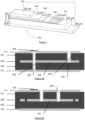
- Figures 2A to E show a partially insulating layer which may be applied between HTS cables to connect them radially.
- the partially insulating layer comprises 5 layers, which are, in order:
- Figures 2 C to E show the layout of the first metal connection layer 211, electrically conducting layer 230, and second metal connection layer 222 respectively.
- Figures 2 A and B are cross sections along the lines A and B in Figures 2 C to E .
- connection layer is present to provide better electrical connection to HTS cables (by soldering or direct contact).
- the electrically conducting layer is divided into several conductive regions. These regions come in two types.
- the square regions 231 (though they may be any shape in practice) are connected by conductive links 206 only to one of the metal connection layers. These regions do not affect the electrical properties of the partially insulating layer, but provide a thermal path through the respective insulating layer. By varying the size of these regions and the number of connections between them and the metal connection layer, the thermal properties of the partially insulating layer can be varied independently of the electrical properties.
- the other regions 232 each connect the first metal connection layer 211 to the second metal connection layer 212, via windows 201, 202 in the first insulating layer 221 and the second insulating layer 222 respectively.
- the resistance between the windows can be controlled by varying the geometry of the regions 232 - e.g. where the region 232 contains an elongated track 233 as shown in Figure 2B , increasing the width of the track would reduce the resistance between the windows, and increasing the length of the track (e.g. by providing a non-linear track, or by moving the windows) would increase the resistance between windows.
- the resistance of the entire partially insulating layer can be controlled by both varying the resistance of each connection between windows, and varying the number of such connections along the partially insulating layer.
- the windows 201 in the first insulating layer are formed by drilled holes through the first connection layer and the first insulating layer, which are then plated with metal 203 (or other electrically conductive material) to connect the first connection layer 211 and the electrically conductive layer 230.
- the windows 202 in the second insulating layer are formed by drilling a hole 202 through all of the layers, which is then plated with metal 204 (or other electrically conductive material).
- the first connection layer is etched around the window 202 to electrically isolate it, and an insulating cap 205 is placed on the end of the window 202 to ensure no bridging occurs due to soldering or contact with the HTS cable.
- the windows 202 may instead be drilled from the other side of the partially insulating layer, such that they pass through the second connection layer, second insulating layer, and electrically conducting layer, and do not pass through (or do not pass completely through) the first insulating layer.
- all the windows may be formed from holes which pass through all layers, with etching of the second connection layer and an insulating cap on the second connection layer being used for windows 201 of the first insulating layer.
- the present disclosure is focussed on detecting that current flow, and using that detection to detect when current sharing is starting to occur in the HTS magnet. Detection of this current sharing mode can be used as an advanced warning of a quench (or potential quench - as used herein, "quench detection” includes the detection of imminent quenches or conditions likely to cause a quench).
- Figure 3 is a circuit diagram representing a partially insulating layer.
- the partially insulating layer has a first track, or "linking track” 301, which connects the HTS cables 311, 312 on either side of the partially insulating layer (equivalently to the tracks 233 in Figure 2 ).
- the partially insulating layer also has a second track, or "pickup track”, 302, which is electrically insulated from the HTS cables 311, 312, and is inductively coupled to the first track (represented by the transformer 303).
- the second track 302 is connected to a current monitor 304. Note that while the resistor and transformer are shown separately in figure 3 , in the examples below the resistance and inductive coupling arise due to the length and shape of the track itself - i.e. the resistor and transformer need not be provided as separate components.
- any change in the current of the first track (e.g. due to a quench) will cause a corresponding change in the current of the second track. This can then be detected by the current monitor, and the measurements from the current monitor can be used by the controller of the magnet to detect a quench.
- the linking and pickup tracks may be shaped to provide greater inductive coupling, e.g. as coils which share a common axis.
- Multiple pickup tracks may be provided (each corresponding to a separate linking track), and connected in parallel to each other and to the current monitor, such that the current monitor measures the total current induced in all the pickup tracks.
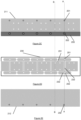
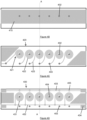
- Figures 4 A to F show an exemplary partially insulating layer implementing the circuit of Figure 3 .
- the partially insulating layer comprises eleven layers, of which there are 6 layers containing electrically conducting elements, each separated by an insulating layer 401 (which may be either an insulator on which the electrically conducting layers are printed, e.g. kapton TM tape, or an insulating adhesive).
- the layers containing electrically conducting elements are, in order:
- Figure 4A is a cross section along the line A-A in Figures 4B to F .
- the first and second metal connection layers 410, 440 are substantially the same as those for the previous example - i.e. they are in place to facilitate electrical connection with the HTS cables.
- the linking track layer contains several linking tracks 421, formed in this examples as spirals 422 having a tail 423.
- the centre of the spiral 422 connects to a conductive link 402 which extends through the insulating layer to connect the linking track 421 to the first metal connection layer, and the opposite end of the tail 423 connects to a conductive link 403 which connects the linking track 421 to the second metal connection layer.
- the conductive links may be formed as holes coated in metal, as with the previous example.
- the pickup track layer 430 contains a pickup track 431 corresponding to each of the linking tracks 421.
- Each pickup track is a spiral of the same dimensions as the corresponding linking track 421, and located directly beneath it.
- Each pickup track is connected to a rail 432 at the outside of the spiral, and to a rail 433 via the inside of the spiral, by way of a conductive link 404 which connects the inside of the spiral to a track 436 in the pickup track connection layer 435, and a conductive link 405 which connects the track 436 to the rail 433.
- connection of the pickup tracks 431 to the rails 432, 433 ensures that the pickup tracks 431 are connected in parallel. This means that, when the rails 432, 433 are connected via a current meter (not shown, but the rails have pads 434 which extend to the edge of the layer to allow connection to rails of other sections of partially insulating layer, or to the current meter), the current measured by the current meter will be the sum of the currents in the pickup tracks.
- the conductive links 403 between the linking track layer and the second metal connection layer also pass through the pickup track layer and the pickup track connection layer, but they are not electrically connected to other elements in those layers.
- the linking and pickup tracks should be arranged such that they do not significantly couple to the magnetic field of the magnet, e.g. having a negligible cross section perpendicular to the local magnetic field. This can be achieved by having them in the plane of the partially insulating layer, as shown in the above examples, but other orientations are also possible.
- Figure 5 shows an alternative arrangement for the linking tracks (which may also be applied to the pickup tracks). Instead of providing curved spiral coils as in Figure 4C , the linking tracks in the linking track layer 520 (which may be substituted for the linking track layer 420 is designs) are provided as square coils 522.
- Figures 6A and 6B show a futher alternative arrangement for the linking tracks.
- the linking track layer 420 of Figure 4A is replaced by first and second linking track layers 620, 625.
- the linking tracks are formed as "butterfly coils" in a "figure-8" pattern. Due to this pattern containing a region where the tracks would cross themselves, it should be arranged in two layers to avoid shorts - one such arrangement is shown in figures 6A and 6B , with the main part of the butterly coil 622 provided on the layer 620, and a crossing tracks 626 provided on a separate layer 625, with conductive links 627 between the crossing tracks and the main part of the butterfly coil.
- Other arrangements which avoid a short are possible, and could be easily envisioned by the skilled person.
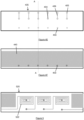
- Figure 7 shows a partially insulating layer 701 comprising:
- the layers are separated by insulating layers 701, as in the previous examples.
- the pickup track layer 710 comprises a pickup track 711 which extends along the coil, in order to couple with the spiral path of the HTS magnet, and conductive links 712 which connect the linking track layer to the outer interface layer (without connecting to the pickup track).
- the pickup track 711 has connection pads 712 at each end, which are then connected to a voltmeter.
- the pickup track 711 is in close proximity to the coil conductor and will inductively couple with it. Voltages that appear across the coil will also appear on this co-wound track, and will be detected by the voltmeter.
- Further connection pads may be provided along the length of the partially insulating layer, allowing it to be easily made in bulk and then cut to length as required for the magnet (i.e. ensuring that a connection pad can be available at the end of the partially insulating layer, whatever the size of the HTS coil).
- the partially insulating layers described above may be made using a flexible PCB manufacturing process, i.e. starting with one of the insulating layers, applying copper to its upper and lower surface, and etching the copper to form two adjacent electrically conducting layers. Further layers may be added by applying further insulating layers and copper layers to the stack (where the insulating layer may be an adhesive used to bond the next copper layer to the stack) and then etching, or by bonding together further copper-clad-and-etched insulating layers (e.g. to form a copper-insulatorcopper-adhesive-copper-insulator-copper construction). Vias can be drilled through the appropriate copper and insulating layers, and then coated with copper to provide connection between copper layers (i.e.
- a via passes through a layer which it should not be electirically connected to, then a region of that layer around the via may be etched to ensure a clear insulating space between the via and electrically conductive components of the layer. Where this occurs on an external layer (e.g. metal connection layers 410, 440), an insulating cap may be affixed to the end of the via to prevent shorts due to soldering or connection to the HTS cable.
- an external layer e.g. metal connection layers 410, 440
- the partially insulating layer may have the same width as the HTS tape.
- the method of winding the HTS pancake coils may involve drawing HTS tape from multiple spools to form a "cable" of many tapes which collect at the coil.
- the partially insulating layer would be fed in with the multi-tape cable to form part of the winding.
- the resulting coil structure would be a multi-tape cable interleaved with the partially insulating layer.
- the tapes and partially insulating layer outer faces are pre-wetted with flux then the wound pack is consolidated with by flooding with solder.
- the coil faces are cleaned afterward to ensure the partially insulating layer layers are not by-passed by solder bridges from turn-to-turn.
- connection layers on the outer surfaces of the partially insulating layers may be omitted, and connection between the linking track layer and the HTS cables made directly through the conductive links, or the partially insulating layer may have the linking and pickup tracks disposed within a solid insulating body rather than the multi-layered structure presented above.
Landscapes
- Engineering & Computer Science (AREA)
- Power Engineering (AREA)
- Physics & Mathematics (AREA)
- Microelectronics & Electronic Packaging (AREA)
- Health & Medical Sciences (AREA)
- High Energy & Nuclear Physics (AREA)
- Spectroscopy & Molecular Physics (AREA)
- General Engineering & Computer Science (AREA)
- Biomedical Technology (AREA)
- General Health & Medical Sciences (AREA)
- Veterinary Medicine (AREA)
- Radiology & Medical Imaging (AREA)
- Life Sciences & Earth Sciences (AREA)
- Animal Behavior & Ethology (AREA)
- Pathology (AREA)
- Public Health (AREA)
- Nuclear Medicine, Radiotherapy & Molecular Imaging (AREA)
- Plasma & Fusion (AREA)
- Optics & Photonics (AREA)
- Manufacturing & Machinery (AREA)
- Particle Accelerators (AREA)
- Superconductors And Manufacturing Methods Therefor (AREA)
- Transformers For Measuring Instruments (AREA)
- Measuring Instrument Details And Bridges, And Automatic Balancing Devices (AREA)
Description
- The present invention relates to high temperature superconducting (HTS) magnets. In particular, the invention relates to a partially insulating layer for use in a partially insulated HTS magnet.
- Superconducting materials are typically divided into "high temperature superconductors" (HTS) and "low temperature superconductors" (LTS). LTS materials, such as Nb and NbTi, are metals or metal alloys whose superconductivity can be described by BCS theory. All low temperature superconductors have a critical temperature (the temperature above which the material cannot be superconducting even in zero magnetic field) below about 30K. The behaviour of HTS material is not described by BCS theory, and such materials may have critical temperatures above about 30K (though it should be noted that it is the physical differences in composition and superconducting operation, rather than the critical temperature, which define HTS and LTS material). The most commonly used HTS are "cuprate superconductors" - ceramics based on cuprates (compounds containing a copper oxide group), such as BSCCO, or ReBCO (where Re is a rare earth element, commonly Y or Gd). Other HTS materials include iron pnictides (e.g. FeAs and FeSe) and magnesium diborate (MgB2).
- ReBCO is typically manufactured as tapes, with a structure as shown in
Figure 1 .Such tape 100 is generally approximately 100 µm thick, and includes a substrate 101 (typically electropolished hastelloy approximately 50 µm thick), on which is deposited by IBAD, magnetron sputtering, or another suitable technique a series of buffer layers known as thebuffer stack 102, of approximate thickness 0.2 µm An epitaxial ReBCO-HTS layer 103 (deposited by MOCVD or another suitable technique) overlays the buffer stack, and is typically 1 µm thick. A 1-2µm silver layer 104 is deposited on the HTS layer by sputtering or another suitable technique, and acopper stabilizer layer 105 is deposited on the tape by electroplating or another suitable technique, which often completely encapsulates the tape. - The
substrate 101 provides a mechanical backbone that can be fed through the manufacturing line and permit growth of subsequent layers. Thebuffer stack 102 is required to provide a biaxially textured crystalline template upon which to grow the HTS layer, and prevents chemical diffusion of elements from the substrate to the HTS which damage its superconducting properties. Thesilver layer 104 is required to provide a low resistance interface from the ReBCO to the stabiliser layer, and thestabiliser layer 105 provides an alternative current path in the event that any part of the ReBCO ceases superconducting (enters the "normal" state). - In addition, "exfoliated" HTS tape can be manufactured, which lacks a substrate and buffer stack, and instead has silver layers on both sides of the HTS layer. Tape which has a substrate will be referred to as "substrated" HTS tape.
- HTS tapes may be arranged into HTS cables. An HTS cable comprises one or more HTS tapes, which are connected along their length by conductive material (normally copper). The HTS tapes may be stacked (i.e. arranged such that the HTS layers are parallel), or they may have some other arrangement of tapes, which may vary along the length of the cable. Notable special cases of HTS cables are single HTS tapes, and HTS pairs. HTS pairs comprise a pair of HTS tapes, arranged such that the HTS layers are parallel. Where substrated tape is used, HTS pairs may be type-0 (with the HTS layers facing each other), type-1 (with the HTS layer of one tape facing the substrate of the other), or type-2 (with the substrates facing each other). Cables comprising more than 2 tapes may arrange some or all of the tapes in HTS pairs. Stacked HTS tapes may comprise various arrangements of HTS pairs, most commonly either a stack of type-1 pairs or a stack of type-0 pairs and (or, equivalently, type-2 pairs). HTS cables may comprise a mix of substrated and exfoliated tape.
- A superconducting magnet is formed by arranging HTS cables (or individual HTS tapes, which for the purpose of this description can be treated as a single-tape cable) into coils, either by winding the HTS cables or by providing sections of the coil made from HTS cables and joining them together. HTS coils come in three broad classes:
- Insulated, having electrically insulating material between the turns (so that current can only flow in the "spiral path" through the HTS cables).
- Non-insulated, where the turns are connected radially, as well as along the cables (e.g. by connecting the copper stabilising layers of the HTS cables).
- Partially insulated, where the turns are connected radially with a controlled resistance, either by the use of materials with a high resistance (e.g. compared to copper), or by providing intermittent insulation between the coils.
- Non-insulated coils could also be considered as the low-resistance case of partially insulated coils. In addition, the insulation can comprise another conductor for quench detection as is disclosed in "Fundamental Evaluations of Applicability of LTS Quench Detectors to REBCO Pancake Coil" by HASEGAWA SHIN ET AL (doi:10.1109/TASC.2019.2900633).
- Having no or partial insulation between turns slows the rate at which the temperature of a local "hotspot" (normal zone) rises. The rate of growth (spatial propagation) of a normal (resistive HTS) zone in an HTS magnet depends on many parameters, but is typically less than 100 mm/s in the axial direction (ie: along the cable), and roughly 2-100 times slower in the transverse direction (ie: between adjacent turns). The exact rate of propagation of the normal zone in each direction depends on the thermal and electrical properties of the materials and cable construction utilised. In particular, the rate of transverse propagation is affected by the thermal properties of the material between turns.
- In a large magnet (linear dimensions of metres, and where the coil cross section dimensions are small (ie ~10 times less) than the largest overall coil dimension) the transverse propagation can cause the entire cross section of the coil to become normal in a zone covering a small fraction of the coil's periphery, resulting in the total current of all turns flowing only in the metal stabilizer within the normal section. Outside the normal zone the conductors are still superconducting. The resistance of this normal zone is not enough to cause the magnet's current to fall quickly but results in the stored magnetic energy of the whole magnet being dumped into this small normal (resistive) volume, which is only growing around the coil periphery slowly. Unless this situation is detected quickly so that the magnet's stored energy can be dumped into a resistance external to the coil, the temperature of the normal zone will rise very quickly, which is likely to cause significant damage to conductors within the normal zone.
- One use of HTS magnets is in tokamak fusion reactors and plasma chambers, particularly in spherical tokamaks. A tokamak has two sets of magnets - poloidal field coils, which are aligned to produce a poloidal field and are generally circular, and toroidal field coils, which comprise a central column and a plurality of return limbs, and are arranged to produce a toroidal field. HTS magnets can be used for either set of field coils, but are particularly useful for toroidal field coils in small tokamaks, as such field coils have tight space limitations which the improved current density and/or reduced cooling requirements of HTS can help with significantly.
- Another potential use of HTS magnets is in proton beam therapy devices. Proton beam therapy (PBT, also known as proton therapy) is a type of particle therapy used in the treatment of cancers (and other conditions which respond to radiotherapy). In PBT, a beam of protons is directed towards the treatment location (e.g. the tumour).
- Another, similar therapy is proton boron capture therapy (PBCT), in which boron-11 is introduced to the target location, and a proton beam is used to initiate the p+11B → 3α reaction. The same apparatus can be used to provide proton beams for either PBT or PBCT.
- The proton beams for PBT and PBCT are generated by particle accelerators such as a cyclotrons or linear accelerators. Accelerators typically used for PBT and PBCT typically produce protons with energies in the range of 60 to 250MeV, with the most powerful currently operating facility having a maximum energy of 400 MeV.
- The design of PBT or PBCT devices requires a gantry to hold electromagnets capable of steering protons at the beam energy. This requires very high magnetic fields, and as such the use of HTS magnets can considerably reduce the mass and size of the electromagnets and the gantry needed to move them. HTS magnets may be used within the accelerator, quadrupole magnets of the steering magnets, or dipole magnets of the steering magnets.
- The invention is set out in independent claims 1 and 7.
- According to a first aspect, there is provided a partially insulating layer for use in ar HTS magnet coil. The partially insulating layer comprises an
insulating body 401 having within it a set of linking tracks and a set of pickup tracks. Each linking track is electrically conductive and is electrically connected to first and second surfaces of the partially insulating layer, in order to provide an electrical path between said first and second surfaces. Each pickup track is electrically conductive and is inductively coupled to a respective linking track, and electrically isolated from the first and second surfaces. Each of the pickup tracks is configured for connection to a current measuring device in order to measure a current induced in the pickup track by a change in current flowing in the respective linking track. - According to a second aspect, there is provided a partially insulating layer for use in an HTS magnet coil. The partially insulating layer comprises an
insulating body 701 having within it a set of linking tracks and a set of pickup tracks. Each linking track is electrically conductive and is electrically connected to first and second surfaces of the partially insulating layer, in order to provide an electrical path between said first and second surfaces. The pickup track is electrically conductive, extends along the length of the partially insulating layer, and is electrically isolated from the first and second surfaces. The pickup track is configured for connection to a voltage measuring device in order to measure a voltage induced in the pickup track by a change in current in an HTS conductor of the HTS magnet coil. - According to a third aspect, there is provided a high temperature superconducting, HTS, field coil comprising one or more HTS cables and one or more partially insulating layers, wherein the one or more HTS cables are arranged to form turns, and the one or more partially insulating layers are arranged to connect the turns radially, wherein the partially insulating layers are partially insulating layers according to the first or second aspect.
- According to a fourth aspect, there is provided a tokamak comprising a toroidal field coil which is an HTS field coil according to the third aspect.
- According to a fifth aspect, there is provided a proton beam therapy, PBT, device comprising an HTS field coil according to the third aspect, wherein the HTS field coil is one of:
- a field coil of an accelerator of the PBT device;
- a dipole or quadrupole magnet of a proton beam steering system of the PBT device.
-
-
Figure 1 is a schematic illustration of an HTS tape; -
Figures 2A to E show a partially insulating layer for an HTS coil; -
Figure 3 shows a circuit diagram illustrating the principle of an exemplary partially insulating layer; -
Figures 4A to F show an exemplary partially insulating layer; -
Figure 5 shows an alternative coil structure; -
Figures 6A and 6B show a further alternative coil structure; and -
Figures 7A and 7B show an alternative construction of a partially insulating layer. -
Figures 2A to E show a partially insulating layer which may be applied between HTS cables to connect them radially. - The partially insulating layer comprises 5 layers, which are, in order:
- a first
metal connection layer 211; - a first insulating
layer 221; - an
electrically conducting layer 230; - a second insulating
layer 222; - a second
metal connection layer 212. -
Figures 2 C to E show the layout of the firstmetal connection layer 211, electrically conductinglayer 230, and secondmetal connection layer 222 respectively.Figures 2 A and B are cross sections along the lines A and B inFigures 2 C to E . - The connection layer is present to provide better electrical connection to HTS cables (by soldering or direct contact).
- The electrically conducting layer is divided into several conductive regions. These regions come in two types. The square regions 231 (though they may be any shape in practice) are connected by
conductive links 206 only to one of the metal connection layers. These regions do not affect the electrical properties of the partially insulating layer, but provide a thermal path through the respective insulating layer. By varying the size of these regions and the number of connections between them and the metal connection layer, the thermal properties of the partially insulating layer can be varied independently of the electrical properties. - The
other regions 232 each connect the firstmetal connection layer 211 to the secondmetal connection layer 212, viawindows layer 221 and the second insulatinglayer 222 respectively. The resistance between the windows can be controlled by varying the geometry of the regions 232 - e.g. where theregion 232 contains anelongated track 233 as shown inFigure 2B , increasing the width of the track would reduce the resistance between the windows, and increasing the length of the track (e.g. by providing a non-linear track, or by moving the windows) would increase the resistance between windows. The resistance of the entire partially insulating layer can be controlled by both varying the resistance of each connection between windows, and varying the number of such connections along the partially insulating layer. - The
windows 201 in the first insulating layer are formed by drilled holes through the first connection layer and the first insulating layer, which are then plated with metal 203 (or other electrically conductive material) to connect thefirst connection layer 211 and the electricallyconductive layer 230. Thewindows 202 in the second insulating layer are formed by drilling ahole 202 through all of the layers, which is then plated with metal 204 (or other electrically conductive material). To prevent a connection being formed to the first connection layer through thewindows 202 of the second insulating layer, the first connection layer is etched around thewindow 202 to electrically isolate it, and aninsulating cap 205 is placed on the end of thewindow 202 to ensure no bridging occurs due to soldering or contact with the HTS cable. - As an alternative, the
windows 202 may instead be drilled from the other side of the partially insulating layer, such that they pass through the second connection layer, second insulating layer, and electrically conducting layer, and do not pass through (or do not pass completely through) the first insulating layer. As a further alternative, all the windows may be formed from holes which pass through all layers, with etching of the second connection layer and an insulating cap on the second connection layer being used forwindows 201 of the first insulating layer. - This implementation and related examples are further described in
EP3747033B1 . - The use of partial insulation will significantly extend the time available to detect a quench, when compared to an equivalent non-insulated coil. However, there is still a need for quench detection methods which are fast enough to detect a hotspot forming in the coil in good time so that countermeasures can be used before damage to the magnet becomes inevitable.
- When current in part of the HTS cable of the coil approaches the critical current of the HTS cable, some of the current will leave the HTS and begin to flow through the stabiliser layers of the cable. At this point current will begin to flow through the resistive and inductive links forming the partial insulation between the HTS turns. The PCB fabricated partial insulation facilitates precise layout and design of the linking tracks allowing for precise setting of the turn-to-turn resistance and linking track inductance.
- The present disclosure is focussed on detecting that current flow, and using that detection to detect when current sharing is starting to occur in the HTS magnet. Detection of this current sharing mode can be used as an advanced warning of a quench (or potential quench - as used herein, "quench detection" includes the detection of imminent quenches or conditions likely to cause a quench).
- The principle is shown schematically in
Figure 3 , which is a circuit diagram representing a partially insulating layer. The partially insulating layer has a first track, or "linking track" 301, which connects theHTS cables tracks 233 inFigure 2 ). The partially insulating layer also has a second track, or "pickup track", 302, which is electrically insulated from theHTS cables second track 302 is connected to acurrent monitor 304. Note that while the resistor and transformer are shown separately infigure 3 , in the examples below the resistance and inductive coupling arise due to the length and shape of the track itself - i.e. the resistor and transformer need not be provided as separate components. - Due to the inductive coupling between the first and second tracks, any change in the current of the first track (e.g. due to a quench) will cause a corresponding change in the current of the second track. This can then be detected by the current monitor, and the measurements from the current monitor can be used by the controller of the magnet to detect a quench.
- Various alterations may be used to improve the sensitivity of the quench detection. For example, the linking and pickup tracks may be shaped to provide greater inductive coupling, e.g. as coils which share a common axis. Multiple pickup tracks may be provided (each corresponding to a separate linking track), and connected in parallel to each other and to the current monitor, such that the current monitor measures the total current induced in all the pickup tracks.
-
Figures 4 A to F show an exemplary partially insulating layer implementing the circuit ofFigure 3 . The partially insulating layer comprises eleven layers, of which there are 6 layers containing electrically conducting elements, each separated by an insulating layer 401 (which may be either an insulator on which the electrically conducting layers are printed, e.g. kapton™ tape, or an insulating adhesive). The layers containing electrically conducting elements are, in order: - A first
metal connection layer 410, shown inFigure 4B . - A linking
track layer 420, shown inFigure 4C . - A
pickup track layer 430, shown inFigure 4D . - A pickup track connection layer, 435, shown in
Figure 4E . - A second
metal connection layer 440, shown inFigure 4F . -
Figure 4A is a cross section along the line A-A inFigures 4B to F . - The first and second metal connection layers 410, 440 are substantially the same as those for the previous example - i.e. they are in place to facilitate electrical connection with the HTS cables.
- The linking track layer contains several linking
tracks 421, formed in this examples asspirals 422 having atail 423. The centre of thespiral 422 connects to aconductive link 402 which extends through the insulating layer to connect the linkingtrack 421 to the first metal connection layer, and the opposite end of thetail 423 connects to aconductive link 403 which connects the linkingtrack 421 to the second metal connection layer. The conductive links may be formed as holes coated in metal, as with the previous example. - The
pickup track layer 430 contains apickup track 431 corresponding to each of the linking tracks 421. Each pickup track is a spiral of the same dimensions as the corresponding linkingtrack 421, and located directly beneath it. Each pickup track is connected to arail 432 at the outside of the spiral, and to arail 433 via the inside of the spiral, by way of aconductive link 404 which connects the inside of the spiral to atrack 436 in the pickuptrack connection layer 435, and aconductive link 405 which connects thetrack 436 to therail 433. - The connection of the pickup tracks 431 to the
rails rails pads 434 which extend to the edge of the layer to allow connection to rails of other sections of partially insulating layer, or to the current meter), the current measured by the current meter will be the sum of the currents in the pickup tracks. - The
conductive links 403 between the linking track layer and the second metal connection layer also pass through the pickup track layer and the pickup track connection layer, but they are not electrically connected to other elements in those layers. - To avoid interference, the linking and pickup tracks should be arranged such that they do not significantly couple to the magnetic field of the magnet, e.g. having a negligible cross section perpendicular to the local magnetic field. This can be achieved by having them in the plane of the partially insulating layer, as shown in the above examples, but other orientations are also possible.
-
Figure 5 shows an alternative arrangement for the linking tracks (which may also be applied to the pickup tracks). Instead of providing curved spiral coils as inFigure 4C , the linking tracks in the linking track layer 520 (which may be substituted for the linkingtrack layer 420 is designs) are provided as square coils 522. -
Figures 6A and 6B show a futher alternative arrangement for the linking tracks. The linkingtrack layer 420 ofFigure 4A is replaced by first and second linking track layers 620, 625. The linking tracks are formed as "butterfly coils" in a "figure-8" pattern. Due to this pattern containing a region where the tracks would cross themselves, it should be arranged in two layers to avoid shorts - one such arrangement is shown infigures 6A and 6B , with the main part of thebutterly coil 622 provided on thelayer 620, and a crossing tracks 626 provided on aseparate layer 625, withconductive links 627 between the crossing tracks and the main part of the butterfly coil. Other arrangements which avoid a short are possible, and could be easily envisioned by the skilled person. - The coil designs in
Figures 4 to 6 are by way of example only. Any arrangement which results in the pickup tracks being sensitive to changes in the current of the linking tracks (i.e. indictively coupled to the linking tracks) can be used to detect current leakage through the partially insualting layer. - An alternative design is shown in
Figure 7 A and B. Figure 7 shows a partially insulatinglayer 701 comprising: - a first metal connection layer (identical to
layer 211 infigures 2A to E ); - an linking track layer (identical to
layer 230 infigures 2A to E ); - a
pickup track layer 710; and - a second metal connection layer (identical to
layer 212 infigures 2A to E ). - The layers are separated by insulating
layers 701, as in the previous examples. - The
pickup track layer 710 comprises apickup track 711 which extends along the coil, in order to couple with the spiral path of the HTS magnet, andconductive links 712 which connect the linking track layer to the outer interface layer (without connecting to the pickup track). Thepickup track 711 hasconnection pads 712 at each end, which are then connected to a voltmeter. Thepickup track 711 is in close proximity to the coil conductor and will inductively couple with it. Voltages that appear across the coil will also appear on this co-wound track, and will be detected by the voltmeter. Further connection pads may be provided along the length of the partially insulating layer, allowing it to be easily made in bulk and then cut to length as required for the magnet (i.e. ensuring that a connection pad can be available at the end of the partially insulating layer, whatever the size of the HTS coil). - The partially insulating layers described above may be made using a flexible PCB manufacturing process, i.e. starting with one of the insulating layers, applying copper to its upper and lower surface, and etching the copper to form two adjacent electrically conducting layers. Further layers may be added by applying further insulating layers and copper layers to the stack (where the insulating layer may be an adhesive used to bond the next copper layer to the stack) and then etching, or by bonding together further copper-clad-and-etched insulating layers (e.g. to form a copper-insulatorcopper-adhesive-copper-insulator-copper construction). Vias can be drilled through the appropriate copper and insulating layers, and then coated with copper to provide connection between copper layers (i.e. the conductive links of the examples above). If a via passes through a layer which it should not be electirically connected to, then a region of that layer around the via may be etched to ensure a clear insulating space between the via and electrically conductive components of the layer. Where this occurs on an external layer (e.g. metal connection layers 410, 440), an insulating cap may be affixed to the end of the via to prevent shorts due to soldering or connection to the HTS cable.
- While the above refers to a single "partially insulating layer" for the coil, it will be appreciated that this may be made up of several sections connected end-to-end, either with connections between the pickup track layers, or with a separate current detector for each section of pickup track layer (or some combination - e.g. a current detector for every N sections).
- The partially insulating layer may have the same width as the HTS tape. The method of winding the HTS pancake coils may involve drawing HTS tape from multiple spools to form a "cable" of many tapes which collect at the coil. The partially insulating layer would be fed in with the multi-tape cable to form part of the winding. The resulting coil structure would be a multi-tape cable interleaved with the partially insulating layer. The tapes and partially insulating layer outer faces are pre-wetted with flux then the wound pack is consolidated with by flooding with solder. The coil faces are cleaned afterward to ensure the partially insulating layer layers are not by-passed by solder bridges from turn-to-turn.
- Once wound and consolidated the end of the partially insulating layer on the outer diameter of the coil is peeled back slightly so that a pair of fine wires can be attached to the contact pads at the end of the pick-up coil layer. This twisted pair of wires links to a current transducer used to detect the signal of current flowing in the leaky insulation.
- The invention is only defined by the appended claims.
- It will be appreciated that the above examples may be modified in simple ways without departing from the principle of the disclosure (i.e. the provision of pickup tracks inductively coupled to either the HTS coil, or the resistive paths through the partially insulating layer). For example, the connection layers on the outer surfaces of the partially insulating layers may be omitted, and connection between the linking track layer and the HTS cables made directly through the conductive links, or the partially insulating layer may have the linking and pickup tracks disposed within a solid insulating body rather than the multi-layered structure presented above.
Claims (15)
- A current carrying assembly for use in a high temperature superconducting, HTS magnet coil, the current carrying assembly comprising a partially insulating layer and first and second HTS cables; wherein the first and second HTS cables are on respective first and second surfaces of the partially insulating layer;the partially insulating layer comprising:
an insulating body (401) having within it:a set of linking tracks (421) wherein each linking track is electrically conductive and is electrically connected to the first and second surfaces of the partially insulating layer, in order to provide an electrical path between said first and second surfaces;a set of pickup tracks (431), wherein each pickup track is electrically conductive and is inductively coupled to a respective linking track, and electrically isolated from the first and second surfaces; andwherein each of the pickup tracks is electrically connected to electrical contacts for connection to a current measuring device; and wherein the electrial contacts are on surfaces of the partially insulating layer other than the first and second surfaces. - A current carrying assembly according to claim 1, wherein the set of pickup tracks is connected in parallel, and is configured to connect in parallel to the current measuring device.
- A current carrying assembly according to claim 2, wherein the pickup tracks are arranged such that, when the partially insulating layer is connected end-to-end to an identical further partially insulating layer, the pickup tracks on both partially insulating layers are connected in parallel with each other and with the current measuring device via the electrical contacts.
- A current carrying assembly according to any preceding claim, wherein each pickup track (431) and each linking track (421) has a section which is a spiral.
- A current carrying assembly according to any of claims 1 to 3, wherein each pickup track and each linking track has a section which is a butterfly coil (622) in the form of a figure 8 pattern.
- A current carrying assembly according to any preceding claim, wherein each linking track is electrically connected to said first and second surfaces by vias which are coated in an electrical conductor.
- A current carrying assembly for use in a high temperature superconducting, HTS, magnet coil, the current carrying assembly comprising a partially insulating layer and first and second HTS cables; wherein the first and second cables are on respective first and second surfaces of the partially insulating layer;the partially insulating layer comprising:
an insulating body (701) having within it:a set of linking tracks (231) wherein each linking track is electrically conductive and is electrically connected to the first and second surfaces of the partially insulating layer, in order to provide an electrical path between said first and second surfaces;a pickup track (711) wherein the pickup track is electrically conductive, extends along a length of the partially insulating layer, and is electrically isolated from the first and second surfaces; andwherein the pickup track has electrical contacts for connection to a voltage measuring device; wherein the electrical contacts are on surfaces of the partially insulating layer other than the first and second surfaces. - A current carrying assembly according to claim 7, wherein the pickup track is arranged such that, when the partially insulating layer is connected end-to-end to an identical further partially insulating layer, the pickup tracks on both partially insulating layers are connected in series with each other and with the voltage measuring device via the electrical contacts.
- A current carrying assembly according to any preceding claim, wherein the partially insulating layer is formed as a plurality of layers, each layer being separated by insulating material, the layers comprising:a linking track layer having within it the linking tracks; anda pickup track layer having within it the pickup tracks;wherein electrical connection between the linking tracks and the first and second surface is achieved by vias through the insulating material, said vias containing electrically conductive material.
- A current carrying assembly according to any preceding claim, and comprising on each of the first and second surface, an electrically conductive connection layer electrically connected on one side to the linking tracks and on the other side to the respective HTS cable.
- An high temperature superconducting, HTS, field coil comprising one or more current carrying assemblies according to any preceding claim, wherein the HTS cables are arranged to form turns, and the partially insulating layers are arranged to connect the turns radially.
- An HTS field coil according to claim 11, wherein the first and the second HTS cables and the partially insulating layer are continuously wound to form the turns.
- An HTS field coil according to claim 11, wherein the first and the second HTS cables and the partially insulating layer are arranged in a plurality of sections connected by joints.
- A tokamak comprising a toroidal field coil which is an HTS field coil according to any of claims 11 to 13.
- A proton beam therapy, PBT, device comprising an HTS field coil according to any of claims 11 to 13, wherein the HTS field coil is one of:a field coil of an accelerator of the PBT device;a dipole or quadrupole magnet of a proton beam steering system of the PBT device.
Applications Claiming Priority (2)
| Application Number | Priority Date | Filing Date | Title |
|---|---|---|---|
| GBGB1904528.5A GB201904528D0 (en) | 2019-04-01 | 2019-04-01 | Partial insulation with diagnostic pickup coils |
| PCT/EP2020/059184 WO2020201316A1 (en) | 2019-04-01 | 2020-03-31 | Partial insulation with diagnostic pickup coils |
Publications (2)
| Publication Number | Publication Date |
|---|---|
| EP3948308A1 EP3948308A1 (en) | 2022-02-09 |
| EP3948308B1 true EP3948308B1 (en) | 2023-05-31 |
Family
ID=66443043
Family Applications (1)
| Application Number | Title | Priority Date | Filing Date |
|---|---|---|---|
| EP20717131.5A Active EP3948308B1 (en) | 2019-04-01 | 2020-03-31 | Partial insulation with diagnostic pickup coils |
Country Status (17)
| Country | Link |
|---|---|
| US (1) | US11398329B2 (en) |
| EP (1) | EP3948308B1 (en) |
| JP (1) | JP7161070B2 (en) |
| KR (1) | KR102471164B1 (en) |
| CN (1) | CN113994218B (en) |
| AR (1) | AR118535A1 (en) |
| AU (1) | AU2020250877B2 (en) |
| BR (1) | BR112021019662A2 (en) |
| CA (1) | CA3135813C (en) |
| EA (1) | EA202192674A1 (en) |
| GB (1) | GB201904528D0 (en) |
| IL (1) | IL286707A (en) |
| MX (1) | MX2021011888A (en) |
| PH (1) | PH12021552481A1 (en) |
| SG (1) | SG11202110797YA (en) |
| TW (1) | TW202042257A (en) |
| WO (1) | WO2020201316A1 (en) |
Families Citing this family (4)
| Publication number | Priority date | Publication date | Assignee | Title |
|---|---|---|---|---|
| EP4128290B1 (en) * | 2020-03-26 | 2025-10-22 | Massachusetts Institute of Technology | Demountable solder joints for coupling superconducting current paths |
| WO2022087323A1 (en) * | 2020-10-21 | 2022-04-28 | The Texas A&M University System | Conformal winding and current-sharing in a dipole magnet using superconducting tape conductor |
| US11887752B2 (en) * | 2020-10-26 | 2024-01-30 | The Texas A&M University System | Blocks-in-conduit cable using high-temperature superconducting tape |
| US12527233B2 (en) | 2022-08-19 | 2026-01-13 | Corning Incorporated | Ceramic sheets and methods of cutting ceramic sheets |
Family Cites Families (21)
| Publication number | Priority date | Publication date | Assignee | Title |
|---|---|---|---|---|
| DE1439487A1 (en) | 1951-01-28 | 1968-11-07 | Siemens Ag | Superconducting magnet coil |
| US5026682A (en) * | 1987-04-13 | 1991-06-25 | International Business Machines Corporation | Devices using high Tc superconductors |
| US5187859A (en) * | 1990-08-23 | 1993-02-23 | The United States Of America As Represented By The United States Department Of Energy | Method of preloading superconducting coils by using materials with different thermal expansion coefficients |
| JPH06112042A (en) * | 1992-09-29 | 1994-04-22 | Toshiba Corp | Quench detector for superconducting coil |
| JP3329127B2 (en) * | 1995-03-24 | 2002-09-30 | 松下電器産業株式会社 | Superconducting oscillator |
| JP2000511338A (en) * | 1996-05-29 | 2000-08-29 | アセア ブラウン ボヴェリ エービー | A rotating electric machine including a high-voltage winding conductor and a winding including the conductor |
| AU718707B2 (en) * | 1996-05-29 | 2000-04-20 | Abb Ab | Insulated conductor for high-voltage windings and a method of manufacturing the same |
| SE9704413D0 (en) * | 1997-02-03 | 1997-11-28 | Asea Brown Boveri | A power transformer / reactor |
| EP1876609A4 (en) | 2005-04-19 | 2014-08-20 | Toshiba Kk | Superconducting coil quench detection method and device, and superconducting power storage unit |
| EP2131407A1 (en) * | 2008-06-05 | 2009-12-09 | Nexans | Superconducting wire with low AC losses |
| KR101118749B1 (en) | 2010-03-02 | 2012-03-13 | 한국전기연구원 | superconducting wire |
| FR2979790B1 (en) * | 2011-09-07 | 2013-10-11 | Commissariat Energie Atomique | CURRENT SENSOR |
| JP5924836B2 (en) * | 2011-10-24 | 2016-05-25 | 国立研究開発法人理化学研究所 | High temperature superconducting coated wire and high temperature superconducting coil having the same |
| CN102645597A (en) * | 2012-04-24 | 2012-08-22 | 中国科学院电工研究所 | Quench propagation velocity measuring device for high-temperature superconducting tapes |
| JP2015225871A (en) * | 2014-05-26 | 2015-12-14 | 住友重機械工業株式会社 | Superconducting electromagnet and charged particle beam medical treatment device |
| US10656185B2 (en) | 2015-07-17 | 2020-05-19 | Mediatek Inc. | Planar differential current pickup for wireless power transmission |
| GB201515978D0 (en) * | 2015-09-09 | 2015-10-21 | Tokamak Energy Ltd | HTS magnet sections |
| JP2018026222A (en) | 2016-08-09 | 2018-02-15 | 古河電気工業株式会社 | Tape type high temperature superconducting wire |
| JP7280274B2 (en) | 2018-02-01 | 2023-05-23 | トカマク エナジー リミテッド | Partially insulated HTS coil |
| US10411321B2 (en) * | 2018-02-15 | 2019-09-10 | International Business Machines Corporation | Circulator for use in superconducting quantum technology |
| GB2582342A (en) * | 2019-03-20 | 2020-09-23 | Siemans Healthcare Ltd | Superconductor current leads |
-
2019
- 2019-04-01 GB GBGB1904528.5A patent/GB201904528D0/en not_active Ceased
-
2020
- 2020-03-30 AR ARP200100885A patent/AR118535A1/en unknown
- 2020-03-31 SG SG11202110797YA patent/SG11202110797YA/en unknown
- 2020-03-31 JP JP2021558552A patent/JP7161070B2/en active Active
- 2020-03-31 MX MX2021011888A patent/MX2021011888A/en unknown
- 2020-03-31 EA EA202192674A patent/EA202192674A1/en unknown
- 2020-03-31 WO PCT/EP2020/059184 patent/WO2020201316A1/en not_active Ceased
- 2020-03-31 CA CA3135813A patent/CA3135813C/en active Active
- 2020-03-31 EP EP20717131.5A patent/EP3948308B1/en active Active
- 2020-03-31 PH PH1/2021/552481A patent/PH12021552481A1/en unknown
- 2020-03-31 KR KR1020217035654A patent/KR102471164B1/en active Active
- 2020-03-31 BR BR112021019662A patent/BR112021019662A2/en not_active Application Discontinuation
- 2020-03-31 AU AU2020250877A patent/AU2020250877B2/en active Active
- 2020-03-31 CN CN202080040569.4A patent/CN113994218B/en active Active
- 2020-03-31 US US17/594,073 patent/US11398329B2/en active Active
- 2020-04-01 TW TW109111259A patent/TW202042257A/en unknown
-
2021
- 2021-09-26 IL IL286707A patent/IL286707A/en unknown
Also Published As
| Publication number | Publication date |
|---|---|
| GB201904528D0 (en) | 2019-05-15 |
| AR118535A1 (en) | 2021-10-20 |
| CN113994218A (en) | 2022-01-28 |
| CA3135813A1 (en) | 2020-10-08 |
| PH12021552481A1 (en) | 2022-06-13 |
| TW202042257A (en) | 2020-11-16 |
| WO2020201316A1 (en) | 2020-10-08 |
| BR112021019662A2 (en) | 2021-12-07 |
| EP3948308A1 (en) | 2022-02-09 |
| JP7161070B2 (en) | 2022-10-25 |
| KR20210144877A (en) | 2021-11-30 |
| SG11202110797YA (en) | 2021-10-28 |
| KR102471164B1 (en) | 2022-11-25 |
| EA202192674A1 (en) | 2021-12-07 |
| MX2021011888A (en) | 2022-10-17 |
| CA3135813C (en) | 2023-01-03 |
| AU2020250877A1 (en) | 2021-11-04 |
| AU2020250877B2 (en) | 2022-11-17 |
| JP2022526797A (en) | 2022-05-26 |
| US11398329B2 (en) | 2022-07-26 |
| US20220148778A1 (en) | 2022-05-12 |
| IL286707A (en) | 2021-10-31 |
| CN113994218B (en) | 2025-01-24 |
Similar Documents
| Publication | Publication Date | Title |
|---|---|---|
| US11101060B2 (en) | Partially-insulated HTS coils | |
| AU2020250877B2 (en) | Partial insulation with diagnostic pickup coils | |
| KR102715485B1 (en) | Fast dump of partially insulated superconducting magnet | |
| US12592332B2 (en) | HTS linked partial insulation for HTS field coils | |
| KR20200128670A (en) | Cryogenic system monitor device | |
| EA040480B1 (en) | CURRENT-CARRYING ASSEMBLY FOR USE IN A MAGNET COIL WITH A HIGH-TEMPERATURE SUPERCONDUCTOR (HTSC) | |
| RU2818160C1 (en) | Hts-related partial insulation for hts excitation coils | |
| CA3090059C (en) | Partially-insulated hts coils | |
| HK40034340B (en) | Partially-insulated hts coils | |
| Sumiyoshi et al. | Sweep-rate dependences of losses in aluminum-stabilized superconducting conductors for the Large Helical Device |
Legal Events
| Date | Code | Title | Description |
|---|---|---|---|
| STAA | Information on the status of an ep patent application or granted ep patent |
Free format text: STATUS: UNKNOWN |
|
| STAA | Information on the status of an ep patent application or granted ep patent |
Free format text: STATUS: THE INTERNATIONAL PUBLICATION HAS BEEN MADE |
|
| PUAI | Public reference made under article 153(3) epc to a published international application that has entered the european phase |
Free format text: ORIGINAL CODE: 0009012 |
|
| STAA | Information on the status of an ep patent application or granted ep patent |
Free format text: STATUS: REQUEST FOR EXAMINATION WAS MADE |
|
| 17P | Request for examination filed |
Effective date: 20210901 |
|
| AK | Designated contracting states |
Kind code of ref document: A1 Designated state(s): AL AT BE BG CH CY CZ DE DK EE ES FI FR GB GR HR HU IE IS IT LI LT LU LV MC MK MT NL NO PL PT RO RS SE SI SK SM TR |
|
| DAV | Request for validation of the european patent (deleted) | ||
| DAX | Request for extension of the european patent (deleted) | ||
| REG | Reference to a national code |
Ref country code: HK Ref legal event code: DE Ref document number: 40070294 Country of ref document: HK |
|
| GRAP | Despatch of communication of intention to grant a patent |
Free format text: ORIGINAL CODE: EPIDOSNIGR1 |
|
| STAA | Information on the status of an ep patent application or granted ep patent |
Free format text: STATUS: GRANT OF PATENT IS INTENDED |
|
| INTG | Intention to grant announced |
Effective date: 20221208 |
|
| GRAS | Grant fee paid |
Free format text: ORIGINAL CODE: EPIDOSNIGR3 |
|
| GRAA | (expected) grant |
Free format text: ORIGINAL CODE: 0009210 |
|
| STAA | Information on the status of an ep patent application or granted ep patent |
Free format text: STATUS: THE PATENT HAS BEEN GRANTED |
|
| AK | Designated contracting states |
Kind code of ref document: B1 Designated state(s): AL AT BE BG CH CY CZ DE DK EE ES FI FR GB GR HR HU IE IS IT LI LT LU LV MC MK MT NL NO PL PT RO RS SE SI SK SM TR |
|
| REG | Reference to a national code |
Ref country code: GB Ref legal event code: FG4D Ref country code: CH Ref legal event code: EP |
|
| REG | Reference to a national code |
Ref country code: DE Ref legal event code: R096 Ref document number: 602020011322 Country of ref document: DE |
|
| REG | Reference to a national code |
Ref country code: AT Ref legal event code: REF Ref document number: 1571220 Country of ref document: AT Kind code of ref document: T Effective date: 20230615 |
|
| P01 | Opt-out of the competence of the unified patent court (upc) registered |
Effective date: 20230512 |
|
| REG | Reference to a national code |
Ref country code: IE Ref legal event code: FG4D |
|
| REG | Reference to a national code |
Ref country code: LT Ref legal event code: MG9D |
|
| REG | Reference to a national code |
Ref country code: NL Ref legal event code: MP Effective date: 20230531 |
|
| REG | Reference to a national code |
Ref country code: AT Ref legal event code: MK05 Ref document number: 1571220 Country of ref document: AT Kind code of ref document: T Effective date: 20230531 |
|
| PG25 | Lapsed in a contracting state [announced via postgrant information from national office to epo] |
Ref country code: SE Free format text: LAPSE BECAUSE OF FAILURE TO SUBMIT A TRANSLATION OF THE DESCRIPTION OR TO PAY THE FEE WITHIN THE PRESCRIBED TIME-LIMIT Effective date: 20230531 Ref country code: NO Free format text: LAPSE BECAUSE OF FAILURE TO SUBMIT A TRANSLATION OF THE DESCRIPTION OR TO PAY THE FEE WITHIN THE PRESCRIBED TIME-LIMIT Effective date: 20230831 Ref country code: ES Free format text: LAPSE BECAUSE OF FAILURE TO SUBMIT A TRANSLATION OF THE DESCRIPTION OR TO PAY THE FEE WITHIN THE PRESCRIBED TIME-LIMIT Effective date: 20230531 Ref country code: AT Free format text: LAPSE BECAUSE OF FAILURE TO SUBMIT A TRANSLATION OF THE DESCRIPTION OR TO PAY THE FEE WITHIN THE PRESCRIBED TIME-LIMIT Effective date: 20230531 |
|
| PG25 | Lapsed in a contracting state [announced via postgrant information from national office to epo] |
Ref country code: RS Free format text: LAPSE BECAUSE OF FAILURE TO SUBMIT A TRANSLATION OF THE DESCRIPTION OR TO PAY THE FEE WITHIN THE PRESCRIBED TIME-LIMIT Effective date: 20230531 Ref country code: PL Free format text: LAPSE BECAUSE OF FAILURE TO SUBMIT A TRANSLATION OF THE DESCRIPTION OR TO PAY THE FEE WITHIN THE PRESCRIBED TIME-LIMIT Effective date: 20230531 Ref country code: NL Free format text: LAPSE BECAUSE OF FAILURE TO SUBMIT A TRANSLATION OF THE DESCRIPTION OR TO PAY THE FEE WITHIN THE PRESCRIBED TIME-LIMIT Effective date: 20230531 Ref country code: LV Free format text: LAPSE BECAUSE OF FAILURE TO SUBMIT A TRANSLATION OF THE DESCRIPTION OR TO PAY THE FEE WITHIN THE PRESCRIBED TIME-LIMIT Effective date: 20230531 Ref country code: LT Free format text: LAPSE BECAUSE OF FAILURE TO SUBMIT A TRANSLATION OF THE DESCRIPTION OR TO PAY THE FEE WITHIN THE PRESCRIBED TIME-LIMIT Effective date: 20230531 Ref country code: IS Free format text: LAPSE BECAUSE OF FAILURE TO SUBMIT A TRANSLATION OF THE DESCRIPTION OR TO PAY THE FEE WITHIN THE PRESCRIBED TIME-LIMIT Effective date: 20230930 Ref country code: HR Free format text: LAPSE BECAUSE OF FAILURE TO SUBMIT A TRANSLATION OF THE DESCRIPTION OR TO PAY THE FEE WITHIN THE PRESCRIBED TIME-LIMIT Effective date: 20230531 Ref country code: GR Free format text: LAPSE BECAUSE OF FAILURE TO SUBMIT A TRANSLATION OF THE DESCRIPTION OR TO PAY THE FEE WITHIN THE PRESCRIBED TIME-LIMIT Effective date: 20230901 |
|
| PG25 | Lapsed in a contracting state [announced via postgrant information from national office to epo] |
Ref country code: FI Free format text: LAPSE BECAUSE OF FAILURE TO SUBMIT A TRANSLATION OF THE DESCRIPTION OR TO PAY THE FEE WITHIN THE PRESCRIBED TIME-LIMIT Effective date: 20230531 |
|
| PG25 | Lapsed in a contracting state [announced via postgrant information from national office to epo] |
Ref country code: SK Free format text: LAPSE BECAUSE OF FAILURE TO SUBMIT A TRANSLATION OF THE DESCRIPTION OR TO PAY THE FEE WITHIN THE PRESCRIBED TIME-LIMIT Effective date: 20230531 |
|
| PG25 | Lapsed in a contracting state [announced via postgrant information from national office to epo] |
Ref country code: SM Free format text: LAPSE BECAUSE OF FAILURE TO SUBMIT A TRANSLATION OF THE DESCRIPTION OR TO PAY THE FEE WITHIN THE PRESCRIBED TIME-LIMIT Effective date: 20230531 Ref country code: SK Free format text: LAPSE BECAUSE OF FAILURE TO SUBMIT A TRANSLATION OF THE DESCRIPTION OR TO PAY THE FEE WITHIN THE PRESCRIBED TIME-LIMIT Effective date: 20230531 Ref country code: RO Free format text: LAPSE BECAUSE OF FAILURE TO SUBMIT A TRANSLATION OF THE DESCRIPTION OR TO PAY THE FEE WITHIN THE PRESCRIBED TIME-LIMIT Effective date: 20230531 Ref country code: PT Free format text: LAPSE BECAUSE OF FAILURE TO SUBMIT A TRANSLATION OF THE DESCRIPTION OR TO PAY THE FEE WITHIN THE PRESCRIBED TIME-LIMIT Effective date: 20231002 Ref country code: EE Free format text: LAPSE BECAUSE OF FAILURE TO SUBMIT A TRANSLATION OF THE DESCRIPTION OR TO PAY THE FEE WITHIN THE PRESCRIBED TIME-LIMIT Effective date: 20230531 Ref country code: DK Free format text: LAPSE BECAUSE OF FAILURE TO SUBMIT A TRANSLATION OF THE DESCRIPTION OR TO PAY THE FEE WITHIN THE PRESCRIBED TIME-LIMIT Effective date: 20230531 Ref country code: CZ Free format text: LAPSE BECAUSE OF FAILURE TO SUBMIT A TRANSLATION OF THE DESCRIPTION OR TO PAY THE FEE WITHIN THE PRESCRIBED TIME-LIMIT Effective date: 20230531 |
|
| REG | Reference to a national code |
Ref country code: DE Ref legal event code: R097 Ref document number: 602020011322 Country of ref document: DE |
|
| PLBE | No opposition filed within time limit |
Free format text: ORIGINAL CODE: 0009261 |
|
| STAA | Information on the status of an ep patent application or granted ep patent |
Free format text: STATUS: NO OPPOSITION FILED WITHIN TIME LIMIT |
|
| PG25 | Lapsed in a contracting state [announced via postgrant information from national office to epo] |
Ref country code: SI Free format text: LAPSE BECAUSE OF FAILURE TO SUBMIT A TRANSLATION OF THE DESCRIPTION OR TO PAY THE FEE WITHIN THE PRESCRIBED TIME-LIMIT Effective date: 20230531 |
|
| 26N | No opposition filed |
Effective date: 20240301 |
|
| PG25 | Lapsed in a contracting state [announced via postgrant information from national office to epo] |
Ref country code: SI Free format text: LAPSE BECAUSE OF FAILURE TO SUBMIT A TRANSLATION OF THE DESCRIPTION OR TO PAY THE FEE WITHIN THE PRESCRIBED TIME-LIMIT Effective date: 20230531 |
|
| REG | Reference to a national code |
Ref country code: CH Ref legal event code: PL |
|
| PG25 | Lapsed in a contracting state [announced via postgrant information from national office to epo] |
Ref country code: BG Free format text: LAPSE BECAUSE OF FAILURE TO SUBMIT A TRANSLATION OF THE DESCRIPTION OR TO PAY THE FEE WITHIN THE PRESCRIBED TIME-LIMIT Effective date: 20230531 |
|
| PG25 | Lapsed in a contracting state [announced via postgrant information from national office to epo] |
Ref country code: LU Free format text: LAPSE BECAUSE OF NON-PAYMENT OF DUE FEES Effective date: 20240331 |
|
| PG25 | Lapsed in a contracting state [announced via postgrant information from national office to epo] |
Ref country code: MC Free format text: LAPSE BECAUSE OF FAILURE TO SUBMIT A TRANSLATION OF THE DESCRIPTION OR TO PAY THE FEE WITHIN THE PRESCRIBED TIME-LIMIT Effective date: 20230531 |
|
| PG25 | Lapsed in a contracting state [announced via postgrant information from national office to epo] |
Ref country code: MC Free format text: LAPSE BECAUSE OF FAILURE TO SUBMIT A TRANSLATION OF THE DESCRIPTION OR TO PAY THE FEE WITHIN THE PRESCRIBED TIME-LIMIT Effective date: 20230531 Ref country code: LU Free format text: LAPSE BECAUSE OF NON-PAYMENT OF DUE FEES Effective date: 20240331 Ref country code: BG Free format text: LAPSE BECAUSE OF FAILURE TO SUBMIT A TRANSLATION OF THE DESCRIPTION OR TO PAY THE FEE WITHIN THE PRESCRIBED TIME-LIMIT Effective date: 20230531 |
|
| REG | Reference to a national code |
Ref country code: BE Ref legal event code: MM Effective date: 20240331 |
|
| PG25 | Lapsed in a contracting state [announced via postgrant information from national office to epo] |
Ref country code: BE Free format text: LAPSE BECAUSE OF NON-PAYMENT OF DUE FEES Effective date: 20240331 |
|
| PG25 | Lapsed in a contracting state [announced via postgrant information from national office to epo] |
Ref country code: IE Free format text: LAPSE BECAUSE OF NON-PAYMENT OF DUE FEES Effective date: 20240331 |
|
| PG25 | Lapsed in a contracting state [announced via postgrant information from national office to epo] |
Ref country code: IE Free format text: LAPSE BECAUSE OF NON-PAYMENT OF DUE FEES Effective date: 20240331 Ref country code: BE Free format text: LAPSE BECAUSE OF NON-PAYMENT OF DUE FEES Effective date: 20240331 Ref country code: CH Free format text: LAPSE BECAUSE OF NON-PAYMENT OF DUE FEES Effective date: 20240331 |
|
| PG25 | Lapsed in a contracting state [announced via postgrant information from national office to epo] |
Ref country code: CY Free format text: LAPSE BECAUSE OF FAILURE TO SUBMIT A TRANSLATION OF THE DESCRIPTION OR TO PAY THE FEE WITHIN THE PRESCRIBED TIME-LIMIT; INVALID AB INITIO Effective date: 20200331 |
|
| PG25 | Lapsed in a contracting state [announced via postgrant information from national office to epo] |
Ref country code: HU Free format text: LAPSE BECAUSE OF FAILURE TO SUBMIT A TRANSLATION OF THE DESCRIPTION OR TO PAY THE FEE WITHIN THE PRESCRIBED TIME-LIMIT; INVALID AB INITIO Effective date: 20200331 |
|
| PG25 | Lapsed in a contracting state [announced via postgrant information from national office to epo] |
Ref country code: TR Free format text: LAPSE BECAUSE OF FAILURE TO SUBMIT A TRANSLATION OF THE DESCRIPTION OR TO PAY THE FEE WITHIN THE PRESCRIBED TIME-LIMIT Effective date: 20230531 |
|
| PGFP | Annual fee paid to national office [announced via postgrant information from national office to epo] |
Ref country code: GB Payment date: 20260324 Year of fee payment: 7 |
|
| PGFP | Annual fee paid to national office [announced via postgrant information from national office to epo] |
Ref country code: DE Payment date: 20260319 Year of fee payment: 7 |
|
| PGFP | Annual fee paid to national office [announced via postgrant information from national office to epo] |
Ref country code: IT Payment date: 20260324 Year of fee payment: 7 |
|
| PGFP | Annual fee paid to national office [announced via postgrant information from national office to epo] |
Ref country code: FR Payment date: 20260323 Year of fee payment: 7 |