EP3945606A1 - Scalable mps device based on sic, mps device manufacturing method and electronic apparatus comprising the mps device - Google Patents
Scalable mps device based on sic, mps device manufacturing method and electronic apparatus comprising the mps device Download PDFInfo
- Publication number
- EP3945606A1 EP3945606A1 EP21187913.5A EP21187913A EP3945606A1 EP 3945606 A1 EP3945606 A1 EP 3945606A1 EP 21187913 A EP21187913 A EP 21187913A EP 3945606 A1 EP3945606 A1 EP 3945606A1
- Authority
- EP
- European Patent Office
- Prior art keywords
- drift layer
- axis
- diode
- implanted region
- mps
- Prior art date
- Legal status (The legal status is an assumption and is not a legal conclusion. Google has not performed a legal analysis and makes no representation as to the accuracy of the status listed.)
- Pending
Links
Images



Classifications
-
- H—ELECTRICITY
- H10—SEMICONDUCTOR DEVICES; ELECTRIC SOLID-STATE DEVICES NOT OTHERWISE PROVIDED FOR
- H10D—INORGANIC ELECTRIC SEMICONDUCTOR DEVICES
- H10D62/00—Semiconductor bodies, or regions thereof, of devices having potential barriers
- H10D62/10—Shapes, relative sizes or dispositions of the regions of the semiconductor bodies; Shapes of the semiconductor bodies
- H10D62/102—Constructional design considerations for preventing surface leakage or controlling electric field concentration
- H10D62/103—Constructional design considerations for preventing surface leakage or controlling electric field concentration for increasing or controlling the breakdown voltage of reverse-biased devices
- H10D62/105—Constructional design considerations for preventing surface leakage or controlling electric field concentration for increasing or controlling the breakdown voltage of reverse-biased devices by having particular doping profiles, shapes or arrangements of PN junctions; by having supplementary regions, e.g. junction termination extension [JTE]
- H10D62/106—Constructional design considerations for preventing surface leakage or controlling electric field concentration for increasing or controlling the breakdown voltage of reverse-biased devices by having particular doping profiles, shapes or arrangements of PN junctions; by having supplementary regions, e.g. junction termination extension [JTE] having supplementary regions doped oppositely to or in rectifying contact with regions of the semiconductor bodies, e.g. guard rings with PN or Schottky junctions
-
- H—ELECTRICITY
- H10—SEMICONDUCTOR DEVICES; ELECTRIC SOLID-STATE DEVICES NOT OTHERWISE PROVIDED FOR
- H10D—INORGANIC ELECTRIC SEMICONDUCTOR DEVICES
- H10D62/00—Semiconductor bodies, or regions thereof, of devices having potential barriers
- H10D62/10—Shapes, relative sizes or dispositions of the regions of the semiconductor bodies; Shapes of the semiconductor bodies
- H10D62/124—Shapes, relative sizes or dispositions of the regions of semiconductor bodies or of junctions between the regions
- H10D62/126—Top-view geometrical layouts of the regions or the junctions
-
- H—ELECTRICITY
- H10—SEMICONDUCTOR DEVICES; ELECTRIC SOLID-STATE DEVICES NOT OTHERWISE PROVIDED FOR
- H10D—INORGANIC ELECTRIC SEMICONDUCTOR DEVICES
- H10D62/00—Semiconductor bodies, or regions thereof, of devices having potential barriers
- H10D62/80—Semiconductor bodies, or regions thereof, of devices having potential barriers characterised by the materials
- H10D62/83—Semiconductor bodies, or regions thereof, of devices having potential barriers characterised by the materials being Group IV materials, e.g. B-doped Si or undoped Ge
- H10D62/832—Semiconductor bodies, or regions thereof, of devices having potential barriers characterised by the materials being Group IV materials, e.g. B-doped Si or undoped Ge being Group IV materials comprising two or more elements, e.g. SiGe
- H10D62/8325—Silicon carbide
-
- H—ELECTRICITY
- H10—SEMICONDUCTOR DEVICES; ELECTRIC SOLID-STATE DEVICES NOT OTHERWISE PROVIDED FOR
- H10D—INORGANIC ELECTRIC SEMICONDUCTOR DEVICES
- H10D64/00—Electrodes of devices having potential barriers
- H10D64/60—Electrodes characterised by their materials
- H10D64/62—Electrodes ohmically coupled to a semiconductor
-
- H—ELECTRICITY
- H10—SEMICONDUCTOR DEVICES; ELECTRIC SOLID-STATE DEVICES NOT OTHERWISE PROVIDED FOR
- H10D—INORGANIC ELECTRIC SEMICONDUCTOR DEVICES
- H10D8/00—Diodes
- H10D8/01—Manufacture or treatment
- H10D8/045—Manufacture or treatment of PN junction diodes
-
- H—ELECTRICITY
- H10—SEMICONDUCTOR DEVICES; ELECTRIC SOLID-STATE DEVICES NOT OTHERWISE PROVIDED FOR
- H10D—INORGANIC ELECTRIC SEMICONDUCTOR DEVICES
- H10D8/00—Diodes
- H10D8/01—Manufacture or treatment
- H10D8/051—Manufacture or treatment of Schottky diodes
-
- H—ELECTRICITY
- H10—SEMICONDUCTOR DEVICES; ELECTRIC SOLID-STATE DEVICES NOT OTHERWISE PROVIDED FOR
- H10D—INORGANIC ELECTRIC SEMICONDUCTOR DEVICES
- H10D8/00—Diodes
- H10D8/60—Schottky-barrier diodes
Definitions
- the present invention relates to a scalable electronic device based on silicon carbide, an electronic device manufacturing method and an electronic apparatus comprising the electronic device.
- the present invention relates to a miniaturizable merged-PiN-Schottky device with reduced current leakages.
- semiconductor materials which have a wide band gap (e.g., which have an energy value Eg of the band gap greater than 1.1 eV), low on-state resistance (R ON ), high thermal conductivity, high operating frequency and high charge carrier saturation velocity, are ideal for producing electronic components, such as diodes or transistors, in particular for power applications.
- a material having said features, and designed to be used for manufacturing electronic components is silicon carbide (SiC).
- SiC silicon carbide
- silicon carbide in its different polytypes (e.g., 3C-SiC, 4H-SiC, 6H-SiC), is preferable to silicon as regards the properties listed previously.
- Electronic devices provided on a silicon-carbide substrate with respect to similar devices provided on a silicon substrate, have numerous advantages, such as low on-state output resistance, low leakage current, high working temperature, and high working frequencies.
- SiC Schottky diodes have demonstrated higher switching performance, making SiC electronic devices especially favorable for high frequency applications.
- the MPS device has at least one Schottky diode and at least one PN diode (i.e. junction and semiconductors) arranged so to be in parallel to each other.
- the MPS device During use in the forward state, due to a lower Schottky diode forward voltage (approximately 0.7 V) with respect to the PN diode forward voltage (approximately 2.5 V), the MPS device operates as a Schottky diode with lower current density (low leakages in on-state, for applied voltages comprised between approximately 0.7 V and approximately 3 V) and assumes the feature of a PN diode, with sufficiently higher current density (e.g., for applied voltages greater than 3 V).
- the MPS device has the high switching speed and the high efficiency typical of Schottky diodes but is also capable of operating at high voltages and currents such as PN diodes (e.g., reaches currents equal to approximately 100 A when biased to approximately 7 V).
- MPS devices In order for the MPS device to work efficiently in the on-state, known MPS devices are designed such that the Schottky diodes have a total junction area greater than a total junction area of the PN diodes. This criterion on the junction areas is also met during the MPS device miniaturization, necessary to optimize the current concentration, the electrical performance and the integration in electronic apparatuses.
- Document JP 2011 142355 A relates to a rectifying element, and more particularly to a rectifying element applied to a power device.
- the aim of the present invention is to provide a scalable MPS device based on SiC, an MPS device manufacturing method and an electronic apparatus comprising the MPS device, such as to overcome the drawbacks of the prior art.
- a scalable MPS device based on SiC, an MPS device manufacturing method and an electronic apparatus comprising the MPS device are provided, as defined in the accompanying claims.
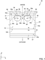
- Figure 1 shows, in lateral-sectional view in a Cartesian (tri-axial) reference system of axes X, Y, Z, a Merged-PiN-Schottky (MPS) device 50 according to an aspect of the present invention.
- the MPS device 50 is shown in Figure 1 in an XZ-plane defined by axes X and Y, and is comprised in an electronic apparatus (not shown, such as notebook, mobile phone, server, TV, automobile, automobile charging station or conversion system for photovoltaic panels).
- the MPS device 50 includes: a substrate 53, of N-type SiC, having a first dopant concentration, provided with a surface 53a opposite to a surface 53b, and thickness between the surfaces 53a and 53b comprised between 50 ⁇ m and 350 ⁇ m, more in particular between 160 ⁇ m and 200 ⁇ m, for example equal to 180 pm; a drift layer (grown in an epitaxial manner) 52, of N-type SiC, having a second dopant concentration smaller than the first dopant concentration and having a top surface 52a and a bottom surface 52b opposite to each other, the drift layer 52 extending on the surface 53a of the substrate 53 (in detail, the surfaces 53a and 52b are in contact to each other) and having a thickness between the surfaces 52a and 53b comprised between 5 and 15 pm; an ohmic contact region, or layer, 56 (e.g.
- a cathode metallization 57 e.g. of Ti/NiV/Ag or Ti/NiV/Au, extending on the ohmic contact region 56; an anode metallization 58, e.g.
- each implanted region 59' of P-type in the drift layer 52 facing the top surface 52a of the drift layer 52 and, for each implanted region 59', a respective ohmic contact 59" such that each implanted region 59' forms a respective junction-barrier (JB) element 59 with the substrate 53; an edge termination region, or protection ring, 60 (optional), in particular a P-type implanted region, completely surrounding the junction-barrier (JB) elements 59; and an insulating layer 61 (optional) extending on the top surface 52a of the drift layer 52 so as to completely surround the JB elements 59, is at least partially superimposed to the protection ring 60 and laterally delimits the anode metallization 58.
- One or more Schottky diodes 62 are formed at the interface between the drift layer 52 and the anode metallization 58, laterally to the implanted regions 59'.
- Schottky (semiconductor-metal) junctions are formed by portions of the drift layer 52 in direct electrical contact with respective portions of the anode metallization 58.
- Figure 1 shows two implanted regions 59' which, with the substrate 53, form respective JB elements 59.
- the JB elements 59 are P-i-N diodes formed by the implanted regions 59', by the drift layer 52 and by the substrate 53.
- the region of the MPS device 50 including the JB elements 59 and the Schottky diodes 62 is an active area 54 of the MPS device 50.
- Each ohmic contact 59" forms an electrical connection having an electrical resistivity value lower than the electrical resistivity value of the implanted region 59' which houses it.
- the ohmic contacts 59" are formed according to prior arts.
- each ohmic contact 59" is formed by one or more carbon-rich layers, including for example graphite layers, or graphene multi-layers.
- the ohmic contacts 59" do not extend, along the Z-axis, beyond the top surface 52a; in other words, the ohmic contacts 59" have respective surfaces 59a coplanar (i.e.
- the ohmic contacts 59" are not in direct physical contact with the drift layer 52 and are physically and electrically separated from the latter through the respective implanted regions 59'.
- each ohmic contact 59" extends in the respective implanted region 59' so as to be surrounded, inferiorly and laterally, by the latter, while the respective surface 59a is in contact with the anode metallization 58. This prevents the anode metallization 58 from forming resistances with the drift layer 52 (instead of the Schottky diodes 62), and the current from flowing both in direct bias condition and in reverse bias condition.
- Figure 2A shows, in plan view from above in an XY-plane defined by the axes X and Y, the MPS device 50 according to an embodiment of the present invention, similar to that shown in Figure 1 .
- the MPS device 50 comprises a plurality of Schottky diodes 62 and JB elements 59 having respective shapes, in the XY-plane, similar to stripes.
- the Schottky diodes 62 and the JB elements 59 have respective main extensions parallel to the Y-axis and are alternated to each other along the X-axis.
- Figure 2B shows, in plan view from above in the XY-plane, the MPS device 50 according to a further embodiment of the present invention, similar to that shown in Figure 1 .
- the MPS device 50 comprises a plurality of Schottky diodes 62 having respective structures, in the XY-plane, similar to cells arranged to form a matrix (or, alternatively, an array).
- each Schottky diode 62 i.e. each cell
- each Schottky diode 62 has, in the XY-plane, a polygonal shape, such as a square shape or a hexagonal shape.
- one or more JB elements 59 surround the Schottky diodes 62 such that the Schottky diodes 62 and the JB elements 59 are alternated to each other both parallel to the X-axis and parallel to the Y-axis.
- each JB element 59 has a width which is minimum parallel to the X-axis at the respective surface 59a, and equal to a first distance (or value) d 1
- each Schottky diode 62 has a respective width which is maximum parallel to the X-axis at the top surface 52a, and equal to a second distance (or value) d 2 . Consequently, considering two Schottky diodes 62 close to each other (i.e.
- these two Schottky diodes 62 have a minimum reciprocal distance along the X-axis equal to the first distance d 1 ; and considering two JB elements 59 close to each other (i.e. facing each other, parallel to the X-axis, through the drift layer 52), these two JB elements 59 have a maximum reciprocal distance along the X-axis equal to the second distance d 2 .
- the second distance d 2 coincides with a diameter, in the XY-plane, of each Schottky diode 62 having said circular shape
- the first distance d 1 is the distance (measured parallel to the X-axis or the Y-axis) between Schottky diodes 62 close to each other in the cell matrix (i.e. immediately subsequent to each other in the cell matrix parallel to the X-axis or the Y-axis).
- each JB element 59 has a first and a second lateral surface 59b, 59c ( Figure 1 ) opposite to each other parallel to the X-axis and adjacent to the surface 59a.
- the lateral surfaces 59b, 59c of the same JB element 59 are distant from each other by the first distance d 1 .
- Two JB elements 59 close to each other have the respective first lateral surfaces 59b (or, alternatively, the respective second lateral surfaces 59c) facing each other and which are distant from each other, at the anode metallization 58, by the second distance d 2 .
- the first distance d 1 is greater than, or equal to, the second distance d 2 .
- the first distance d 1 is comprised between approximately 2 ⁇ m and approximately 3 ⁇ m
- the second distance d 2 is comprised between approximately 1.5 ⁇ m and approximately 1.8 ⁇ m.
- an overall extension area of the Schottky diodes 62 is smaller than or equal to an overall extension area of the JB elements 59.
- said second dopant concentration of the drift layer 52 is greater than the dopant concentration commonly used in the drift layer of the known MPS devices.
- the second dopant concentration is such that a breakdown voltage of the MPS device 50 is greater than, or equal to, 115% of a maximum working voltage of the MPS device 50 in an inhibition state (i.e. in reverse bias).
- the second dopant concentration is such that the breakdown voltage (i.e. the voltage, applicable to the MPS device 50 in an inhibition state, beyond which a charge carrier multiplication phenomenon occurs with consequent sharp increase, in absolute value, in the current of the device MPS 50) exceeds said maximum working voltage in inhibition state by, at most, 15% of the latter.
- the maximum working voltage is equal to a repetitive peak reverse voltage (V RRM ) of the MPS device 50, per se known.
- the breakdown voltage is inversely proportional (in detail, in a linear manner) to the second dopant concentration. For example, when the second dopant concentration is equal to approximately 2.8 ⁇ e 16 at/cm 3 , the breakdown voltage is equal to approximately 760 V; and when the second dopant concentration is equal to approximately 2 ⁇ e 16 at/cm 3 , the breakdown voltage is equal to approximately 880 V.
- the second dopant concentration varies between approximately 2 ⁇ e 16 at/cm 3 and approximately 2.8 ⁇ e 16 at/cm 3 to ensure that the breakdown voltage of the MPS device 50 is greater than, or equal to, approximately 750 V.
- the second dopant concentration is smaller than, or equal to, approximately 1.2 ⁇ e 16 at/cm 3 (e.g., it varies between approximately 5 ⁇ e 15 at/cm 3 and approximately 1.2 ⁇ e 16 at/cm 3 ) to ensure that the breakdown voltage of the MPS device 50 is greater than, or equal to, approximately 1380 V.
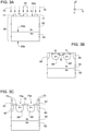
- a wafer 80 including the substrate 53 of SiC (in particular 4H-SiC, although other polytypes such as, but not limited to, 2H-SiC, 3C-SiC and 6H-SiC, may be used), is arranged.
- the substrate 53 has a N-type dopant concentration comprised between 1 ⁇ 10 19 at/cm 3 and 1 ⁇ 10 22 at/cm 3 , and has a thickness, measured along the Z-axis between the surfaces 53a and 53b, comprised between 300 ⁇ m and 450 ⁇ m, and in particular equal to approximately 360 ⁇ m.
- the drift layer 52 is formed, on the surface 53a of the substrate 53, for example through epitaxial growth, having a N-type dopant concentration such that the breakdown voltage of the MPS device 50 is greater than, or equal to, 115% of the maximum working voltage in inhibition state of the MPS device 50, as previously described.
- the drift layer 52 is of SiC, in particular 4H-SiC, but other SiC polytypes, such as 2H, 6H, 3C or 15R, may be used.
- a hard mask 71 is formed, on the surface 52a of the drift layer 52, for example through deposition of a photoresist, or TEOS, or another material suitable for the purpose.
- the hard mask 71 has a thickness between 0.5 ⁇ m and 2 ⁇ m or, in any case, a thickness such as to shield the implant described hereinbelow with reference to Figure 3B .
- the hard mask 71 extends in a region of the wafer 80 wherein, in subsequent steps, the active area 54 of the MPS device 50 will be formed.
- the hard mask 70 covers regions of the surface 52a of the drift layer 52 which will form Schottky diodes 62 and leaves exposed regions of the surface 52a of the drift layer 52 which will form the implanted regions 59'.
- a step of implanting doping species e.g., boron or aluminium
- the second type of conductivity here, P
- the hard mask 71 the implant is indicated in the figure by arrows 70.
- the protection ring 60 if any, is also formed.
- the implanting step 70 comprises one or more implants of P-type doping species, with implant energy comprised between 30 keV and 400 keV and with doses between 1 ⁇ 10 12 at/cm 2 and 1 ⁇ 10 15 at/cm 2 , to form the implanted regions 59' with a dopant concentration greater than 1 ⁇ 10 18 at/cm 3 .
- implanted regions having depth, measured from the surface 52a, comprised between 0.4 ⁇ m and 1 ⁇ m, are formed.
- FIG. 3B The implanted regions 59' and the protection ring 60 are shown in Figure 3B , wherein the hard mask 71 is removed.
- Figure 3B shows that the first distance d 1 is greater than the second distance d 2 .
- the first distance d 1 is equal to the second distance d 2 .
- a thermal annealing step is carried out at the surface 52a for the activation of the doping species implanted in the step of Figure 3A .
- the thermal annealing is, for example, carried out at a temperature higher than 1500°C (e.g., between 1700°C and 1900°C).
- the insulating layer 61 if any, is formed.
- the insulating layer 61 is, at least partially, superimposed to the protection ring 60 and defines with the latter the active area 54 of the MPS device 50.
- a deposition mask 73 of silicon oxide or TEOS is formed to cover surface regions of the drift layer 52 different from the implanted regions 59' (and of the protection ring 60, if any).
- the mask 73 has through openings 73a at portions of the implanted regions 59', which will become the ohmic contacts 59".
- a nickel deposition is carried out on the mask 73 and within the through openings 73a (metal layer 74 in Figure 3D ).
- the nickel thus deposited reaches and contacts the implanted regions 59' through the through openings 73a.
- a subsequent high temperature thermal annealing (between 900°C and 1200°C for a time interval from 1 minute to 120 minutes), allows the ohmic contacts 59" of nickel silicide to be formed, by chemical reaction, between the deposited nickel and the silicon of the drift layer 52 at the through openings 73a.
- the deposited nickel reacts where it is in contact with the surface material of the drift layer 52, forming Ni 2 Si (i.e., the ohmic contact 59").
- a step of removing the metal layer 74, which extends above the mask 73 and the ohmic contacts 59" is carried out.
- a step of grinding the substrate 53 is carried out at the surface 53b, so as to reduce the thickness of the substrate 53.
- the substrate 53 has thickness, measured along the Z-axis between the surfaces 53a and 53b, comprised between 100 ⁇ m and 250 ⁇ m, and in particular equal to approximately 180 ⁇ m.
- the ohmic contact layer 56 from the surface 53b of the substrate 53 (process similar to what described with reference to Figures 3C-3E ), and the cathode metallization 57 from the ohmic contact layer 56 are then formed in succession to each other.
- a step of removing the mask 73 is carried out. Furthermore, the anode metallization 58 is formed on the ohmic contacts 59" and on the regions previously covered by the mask 73. For example, Ti/AlSiCu or Ni/AlSiCu are deposited on the surface 52a of the drift layer 52 such that the anode metallization 58 contacts the drift layer 52 and the JB elements 59.
- the passivation layer 69 (not shown in Figure 3G ) is formed on the anode metallization 58 and on the insulating layer 61, obtaining the MPS device 50 shown in Figure 1 .
- the MPS device 50 since in the MPS device 50 the first distance d 1 is greater than, or equal to, the second distance d 2 , the MPS device 50 is less subject to the lithographic limitations of the known MPS devices related to the formation of the ohmic contacts 59", and therefore it is more scalable. Consequently, the MPS device 50 allows an optimal use of the wafer area (ensuring a higher integration density), and allows a reduction of manufacturing costs and improved electrical performance.
- the high doping species concentration of the drift layer 52 allows a high on-state current flow (i.e. a high surge peak forward current, IFSM, parameter) and prevents the higher ratio between the JB elements 59 and Schottky diodes 62 in the area from leading to degraded electrical performance.
- IFSM surge peak forward current
- the only parameter affecting the design and calculation of the second dopant concentration is the desired breakdown voltage of the MPS device 50.
- the MPS device 50 has therefore less stringent design limits with respect to the known MPS devices, wherein the dopant concentration of the drift layer affects both the breakdown voltage and, above all, the current leakages.
- the MPS device 50 allows reduced current leakages due to a higher pinching efficiency operated by the JB elements 59 on the Schottky diodes 62.
- the first distance d 1 is greater than, or equal to, the second distance d 2 , in use the voltage drops are mainly borne by the JB elements 59 and, therefore, there is a reduced electrical field at the surface 52a of the drift layer 52 and, in particular, at the Schottky diodes 62.
- the conductivities described with reference to Figure 1 may be inverted to each other with respect to what previously described.
- the drift layer 52 and the substrate 53 are of P-type
- the implanted regions 59' and, if any, the protection ring 60 are of N-type.
Landscapes
- Electrodes Of Semiconductors (AREA)
- Semiconductor Integrated Circuits (AREA)
- Apparatuses And Processes For Manufacturing Resistors (AREA)
Abstract
Description
- The present invention relates to a scalable electronic device based on silicon carbide, an electronic device manufacturing method and an electronic apparatus comprising the electronic device. In particular, the present invention relates to a miniaturizable merged-PiN-Schottky device with reduced current leakages.
- As is known, semiconductor materials, which have a wide band gap (e.g., which have an energy value Eg of the band gap greater than 1.1 eV), low on-state resistance (RON), high thermal conductivity, high operating frequency and high charge carrier saturation velocity, are ideal for producing electronic components, such as diodes or transistors, in particular for power applications. A material having said features, and designed to be used for manufacturing electronic components, is silicon carbide (SiC). In particular, silicon carbide, in its different polytypes (e.g., 3C-SiC, 4H-SiC, 6H-SiC), is preferable to silicon as regards the properties listed previously.
- Electronic devices provided on a silicon-carbide substrate, with respect to similar devices provided on a silicon substrate, have numerous advantages, such as low on-state output resistance, low leakage current, high working temperature, and high working frequencies. In particular, SiC Schottky diodes have demonstrated higher switching performance, making SiC electronic devices especially favorable for high frequency applications.
- Merged-PiN-Schottky (MPS) devices based on SiC are also known. The MPS device has at least one Schottky diode and at least one PN diode (i.e. junction and semiconductors) arranged so to be in parallel to each other.
- During use in the forward state, due to a lower Schottky diode forward voltage (approximately 0.7 V) with respect to the PN diode forward voltage (approximately 2.5 V), the MPS device operates as a Schottky diode with lower current density (low leakages in on-state, for applied voltages comprised between approximately 0.7 V and approximately 3 V) and assumes the feature of a PN diode, with sufficiently higher current density (e.g., for applied voltages greater than 3 V). In this manner, the MPS device has the high switching speed and the high efficiency typical of Schottky diodes but is also capable of operating at high voltages and currents such as PN diodes (e.g., reaches currents equal to approximately 100 A when biased to approximately 7 V).
- In order for the MPS device to work efficiently in the on-state, known MPS devices are designed such that the Schottky diodes have a total junction area greater than a total junction area of the PN diodes. This criterion on the junction areas is also met during the MPS device miniaturization, necessary to optimize the current concentration, the electrical performance and the integration in electronic apparatuses.
- However, there are technological limits, due to the lithographic processes currently used in the MPS device manufacturing, thereby arbitrarily decreasing the junction area of the PN diodes is not possible. In particular, an excessive scaling of the MPS device would cause a high risk of short circuit between ohmic contacts of the PN diodes and the Schottky diodes, which would cause damage to the MPS device.
- As a result, in the design of known MPS devices there is a tradeoff between the achievable miniaturization and the electrical performance to be obtained.
- Document
JP 2011 142355 A - The aim of the present invention is to provide a scalable MPS device based on SiC, an MPS device manufacturing method and an electronic apparatus comprising the MPS device, such as to overcome the drawbacks of the prior art.
- According to the present invention a scalable MPS device based on SiC, an MPS device manufacturing method and an electronic apparatus comprising the MPS device are provided, as defined in the accompanying claims.
- For a better understanding of the present invention, preferred embodiments thereof are now described, purely by way of non-limiting example, with reference to the accompanying drawings, wherein:
-
Figure 1 shows, in cross-sectional view, an MPS device according to an embodiment of the present invention; -
Figures 2A and 2B show, in plan view from above, the MPS device ofFigure 1 , according to respective embodiments of the present invention; -
Figure 2C is a diagram schematically illustrating the dependence of a breakdown voltage of the MPS device ofFigure 1 on a dopant concentration of a drift layer of said MPS device, according to an embodiment of the present invention; and -
Figures 3A-3G show, in cross-sectional view, respective manufacturing steps of the MPS device ofFigure 1 , according to an embodiment of the present invention. - Elements common to the different embodiments of the present invention, described hereinbelow, are indicated with the same reference numbers.
-
Figure 1 shows, in lateral-sectional view in a Cartesian (tri-axial) reference system of axes X, Y, Z, a Merged-PiN-Schottky (MPS)device 50 according to an aspect of the present invention. In particular, theMPS device 50 is shown inFigure 1 in an XZ-plane defined by axes X and Y, and is comprised in an electronic apparatus (not shown, such as notebook, mobile phone, server, TV, automobile, automobile charging station or conversion system for photovoltaic panels). - The
MPS device 50 includes: asubstrate 53, of N-type SiC, having a first dopant concentration, provided with asurface 53a opposite to asurface 53b, and thickness between thesurfaces top surface 52a and abottom surface 52b opposite to each other, thedrift layer 52 extending on thesurface 53a of the substrate 53 (in detail, thesurfaces surfaces surface 53b of thesubstrate 53; acathode metallization 57, e.g. of Ti/NiV/Ag or Ti/NiV/Au, extending on theohmic contact region 56; ananode metallization 58, e.g. of Ti/AlSiCu or Ni/AlSiCu, extending on thetop surface 52a of thedrift layer 52; apassivation layer 69 extending on theanode metallization 58, to protect the latter; at least one implanted region 59' of P-type in thedrift layer 52, facing thetop surface 52a of thedrift layer 52 and, for each implanted region 59', a respectiveohmic contact 59" such that each implanted region 59' forms a respective junction-barrier (JB)element 59 with thesubstrate 53; an edge termination region, or protection ring, 60 (optional), in particular a P-type implanted region, completely surrounding the junction-barrier (JB)elements 59; and an insulating layer 61 (optional) extending on thetop surface 52a of thedrift layer 52 so as to completely surround theJB elements 59, is at least partially superimposed to theprotection ring 60 and laterally delimits theanode metallization 58. - One or more Schottky
diodes 62 are formed at the interface between thedrift layer 52 and theanode metallization 58, laterally to the implanted regions 59'. In particular, Schottky (semiconductor-metal) junctions are formed by portions of thedrift layer 52 in direct electrical contact with respective portions of theanode metallization 58. - In particular,
Figure 1 shows two implanted regions 59' which, with thesubstrate 53, formrespective JB elements 59. In more detail, theJB elements 59 are P-i-N diodes formed by the implanted regions 59', by thedrift layer 52 and by thesubstrate 53. - The region of the
MPS device 50 including theJB elements 59 and the Schottky diodes 62 (i.e., the region contained within the protection ring 60) is anactive area 54 of theMPS device 50. - Each
ohmic contact 59" forms an electrical connection having an electrical resistivity value lower than the electrical resistivity value of the implanted region 59' which houses it. Theohmic contacts 59" are formed according to prior arts. For example, eachohmic contact 59" is formed by one or more carbon-rich layers, including for example graphite layers, or graphene multi-layers. Alternatively, as shown inFigure 1 , theohmic contacts 59" do not extend, along the Z-axis, beyond thetop surface 52a; in other words, theohmic contacts 59" haverespective surfaces 59a coplanar (i.e. aligned along the X-axis) with thetop surface 52a, and extend in depth (along the Z-axis) within the respective implanted regions 59' for a depth comprised between one nanometer and some tens of nanometers (e.g., between 1 and 20 nm) measured from thetop surface 52a. Furthermore, theohmic contacts 59" are not in direct physical contact with thedrift layer 52 and are physically and electrically separated from the latter through the respective implanted regions 59'. For example, as shown inFigure 1 , eachohmic contact 59" extends in the respective implanted region 59' so as to be surrounded, inferiorly and laterally, by the latter, while therespective surface 59a is in contact with theanode metallization 58. This prevents theanode metallization 58 from forming resistances with the drift layer 52 (instead of the Schottky diodes 62), and the current from flowing both in direct bias condition and in reverse bias condition. -
Figure 2A shows, in plan view from above in an XY-plane defined by the axes X and Y, theMPS device 50 according to an embodiment of the present invention, similar to that shown inFigure 1 . - In
Figure 2A , theMPS device 50 comprises a plurality of Schottkydiodes 62 andJB elements 59 having respective shapes, in the XY-plane, similar to stripes. In particular, in the XY-plane the Schottkydiodes 62 and theJB elements 59 have respective main extensions parallel to the Y-axis and are alternated to each other along the X-axis. -
Figure 2B shows, in plan view from above in the XY-plane, theMPS device 50 according to a further embodiment of the present invention, similar to that shown inFigure 1 . - In
Figure 2B , theMPS device 50 comprises a plurality of Schottkydiodes 62 having respective structures, in the XY-plane, similar to cells arranged to form a matrix (or, alternatively, an array). In particular, in the XY-plane each Schottky diode 62 (i.e. each cell) has a circular shape. Alternatively, each Schottkydiode 62 has, in the XY-plane, a polygonal shape, such as a square shape or a hexagonal shape. Furthermore, one ormore JB elements 59 surround the Schottkydiodes 62 such that the Schottkydiodes 62 and theJB elements 59 are alternated to each other both parallel to the X-axis and parallel to the Y-axis. - As shown in
Figures 1-2B , eachJB element 59 has a width which is minimum parallel to the X-axis at therespective surface 59a, and equal to a first distance (or value) d1, and each Schottkydiode 62 has a respective width which is maximum parallel to the X-axis at thetop surface 52a, and equal to a second distance (or value) d2. Consequently, considering two Schottkydiodes 62 close to each other (i.e. facing each other, parallel to the X-axis, through the same JB element 59), these two Schottkydiodes 62 have a minimum reciprocal distance along the X-axis equal to the first distance d1; and considering twoJB elements 59 close to each other (i.e. facing each other, parallel to the X-axis, through the drift layer 52), these twoJB elements 59 have a maximum reciprocal distance along the X-axis equal to the second distance d2. In particular, inFigure 2B , the second distance d2 coincides with a diameter, in the XY-plane, of each Schottkydiode 62 having said circular shape, and the first distance d1 is the distance (measured parallel to the X-axis or the Y-axis) between Schottkydiodes 62 close to each other in the cell matrix (i.e. immediately subsequent to each other in the cell matrix parallel to the X-axis or the Y-axis). - In more detail, each
JB element 59 has a first and a secondlateral surface Figure 1 ) opposite to each other parallel to the X-axis and adjacent to thesurface 59a. Thelateral surfaces same JB element 59 are distant from each other by the first distance d1. TwoJB elements 59 close to each other have the respective firstlateral surfaces 59b (or, alternatively, the respective secondlateral surfaces 59c) facing each other and which are distant from each other, at theanode metallization 58, by the second distance d2. - According to the present invention, the first distance d1 is greater than, or equal to, the second distance d2. For example, the first distance d1 is comprised between approximately 2 µm and approximately 3 µm, and the second distance d2 is comprised between approximately 1.5 µm and approximately 1.8 µm.
- Consequently, at the
top surface 52a, an overall extension area of the Schottkydiodes 62 is smaller than or equal to an overall extension area of theJB elements 59. - Furthermore, said second dopant concentration of the
drift layer 52 is greater than the dopant concentration commonly used in the drift layer of the known MPS devices. - According to the present invention, the second dopant concentration is such that a breakdown voltage of the
MPS device 50 is greater than, or equal to, 115% of a maximum working voltage of theMPS device 50 in an inhibition state (i.e. in reverse bias). In other words, the second dopant concentration is such that the breakdown voltage (i.e. the voltage, applicable to theMPS device 50 in an inhibition state, beyond which a charge carrier multiplication phenomenon occurs with consequent sharp increase, in absolute value, in the current of the device MPS 50) exceeds said maximum working voltage in inhibition state by, at most, 15% of the latter. In particular, the maximum working voltage is equal to a repetitive peak reverse voltage (VRRM) of theMPS device 50, per se known. - In more detail, as shown in
Figure 2C , the breakdown voltage is inversely proportional (in detail, in a linear manner) to the second dopant concentration. For example, when the second dopant concentration is equal to approximately 2.8·e16 at/cm3, the breakdown voltage is equal to approximately 760 V; and when the second dopant concentration is equal to approximately 2·e16 at/cm3, the breakdown voltage is equal to approximately 880 V. - According to one embodiment, when the maximum working voltage of the
MPS device 50 in the inhibition state is to be equal to approximately 650 V and said thickness of thedrift layer 52 is equal to approximately 5 µm, the second dopant concentration varies between approximately 2·e16 at/cm3 and approximately 2.8·e16 at/cm3 to ensure that the breakdown voltage of theMPS device 50 is greater than, or equal to, approximately 750 V. - According to a further embodiment, when the maximum working voltage of the
MPS device 50 in an inhibition state is to be equal to approximately 1200 V and said thickness of thedrift layer 52 is equal to approximately 9 µm, the second dopant concentration is smaller than, or equal to, approximately 1.2·e16 at/cm3 (e.g., it varies between approximately 5·e15 at/cm3 and approximately 1.2·e16 at/cm3) to ensure that the breakdown voltage of theMPS device 50 is greater than, or equal to, approximately 1380 V. - The manufacturing steps of the
MPS device 50 are described hereinbelow, with reference toFigures 3A-3G . - With reference to
Figure 3A , awafer 80, including thesubstrate 53 of SiC (in particular 4H-SiC, although other polytypes such as, but not limited to, 2H-SiC, 3C-SiC and 6H-SiC, may be used), is arranged. For example, thesubstrate 53 has a N-type dopant concentration comprised between 1·1019 at/cm3 and 1·1022 at/cm3, and has a thickness, measured along the Z-axis between thesurfaces - The
drift layer 52 is formed, on thesurface 53a of thesubstrate 53, for example through epitaxial growth, having a N-type dopant concentration such that the breakdown voltage of theMPS device 50 is greater than, or equal to, 115% of the maximum working voltage in inhibition state of theMPS device 50, as previously described. Thedrift layer 52 is of SiC, in particular 4H-SiC, but other SiC polytypes, such as 2H, 6H, 3C or 15R, may be used. - A
hard mask 71 is formed, on thesurface 52a of thedrift layer 52, for example through deposition of a photoresist, or TEOS, or another material suitable for the purpose. Thehard mask 71 has a thickness between 0.5 µm and 2 µm or, in any case, a thickness such as to shield the implant described hereinbelow with reference toFigure 3B . Thehard mask 71 extends in a region of thewafer 80 wherein, in subsequent steps, theactive area 54 of theMPS device 50 will be formed. In plan view, on the XY-plane, thehard mask 70 covers regions of thesurface 52a of thedrift layer 52 which will formSchottky diodes 62 and leaves exposed regions of thesurface 52a of thedrift layer 52 which will form the implanted regions 59'. - Then, a step of implanting doping species (e.g., boron or aluminium), which have the second type of conductivity (here, P), is carried out, exploiting the hard mask 71 (the implant is indicated in the figure by arrows 70). During the step of
Figure 3A , theprotection ring 60, if any, is also formed. - In an exemplary embodiment, the implanting
step 70 comprises one or more implants of P-type doping species, with implant energy comprised between 30 keV and 400 keV and with doses between 1·1012 at/cm2 and 1·1015 at/cm2, to form the implanted regions 59' with a dopant concentration greater than 1·1018 at/cm3. Thus, implanted regions having depth, measured from thesurface 52a, comprised between 0.4 µm and 1 µm, are formed. - The implanted regions 59' and the
protection ring 60 are shown inFigure 3B , wherein thehard mask 71 is removed. In particular,Figure 3B shows that the first distance d1 is greater than the second distance d2. Alternatively, the first distance d1 is equal to the second distance d2. - In
Figure 3B , a thermal annealing step is carried out at thesurface 52a for the activation of the doping species implanted in the step ofFigure 3A . The thermal annealing is, for example, carried out at a temperature higher than 1500°C (e.g., between 1700°C and 1900°C). - With reference to
Figures 3C-3E , further steps are then carried out for the formation of theohmic contacts 59". - With reference to
Figure 3C , the insulatinglayer 61, if any, is formed. The insulatinglayer 61 is, at least partially, superimposed to theprotection ring 60 and defines with the latter theactive area 54 of theMPS device 50. - Furthermore, with reference to
Figure 3C , adeposition mask 73 of silicon oxide or TEOS is formed to cover surface regions of thedrift layer 52 different from the implanted regions 59' (and of theprotection ring 60, if any). In other words, themask 73 has throughopenings 73a at portions of the implanted regions 59', which will become theohmic contacts 59". - Then,
Figure 3D , a nickel deposition is carried out on themask 73 and within the throughopenings 73a (metal layer 74 inFigure 3D ). The nickel thus deposited reaches and contacts the implanted regions 59' through the throughopenings 73a. - With reference to
Figure 3E , a subsequent high temperature thermal annealing (between 900°C and 1200°C for a time interval from 1 minute to 120 minutes), allows theohmic contacts 59" of nickel silicide to be formed, by chemical reaction, between the deposited nickel and the silicon of thedrift layer 52 at the throughopenings 73a. In fact, the deposited nickel reacts where it is in contact with the surface material of thedrift layer 52, forming Ni2Si (i.e., theohmic contact 59"). Subsequently, a step of removing themetal layer 74, which extends above themask 73 and theohmic contacts 59", is carried out. - With reference to
Figure 3F , a step of grinding thesubstrate 53 is carried out at thesurface 53b, so as to reduce the thickness of thesubstrate 53. For example, at the end of the grinding step thesubstrate 53 has thickness, measured along the Z-axis between thesurfaces ohmic contact layer 56 from thesurface 53b of the substrate 53 (process similar to what described with reference toFigures 3C-3E ), and thecathode metallization 57 from theohmic contact layer 56 are then formed in succession to each other. - With reference to
Figure 3G , a step of removing themask 73 is carried out. Furthermore, theanode metallization 58 is formed on theohmic contacts 59" and on the regions previously covered by themask 73. For example, Ti/AlSiCu or Ni/AlSiCu are deposited on thesurface 52a of thedrift layer 52 such that theanode metallization 58 contacts thedrift layer 52 and theJB elements 59. - Then, the passivation layer 69 (not shown in
Figure 3G ) is formed on theanode metallization 58 and on the insulatinglayer 61, obtaining theMPS device 50 shown inFigure 1 . - From a discussion of the features of the invention provided according to the present description, the advantages that it achieves are apparent.
- In particular, since in the
MPS device 50 the first distance d1 is greater than, or equal to, the second distance d2, theMPS device 50 is less subject to the lithographic limitations of the known MPS devices related to the formation of theohmic contacts 59", and therefore it is more scalable. Consequently, theMPS device 50 allows an optimal use of the wafer area (ensuring a higher integration density), and allows a reduction of manufacturing costs and improved electrical performance. - Furthermore, the high doping species concentration of the
drift layer 52 allows a high on-state current flow (i.e. a high surge peak forward current, IFSM, parameter) and prevents the higher ratio between theJB elements 59 andSchottky diodes 62 in the area from leading to degraded electrical performance. - In more detail, the only parameter affecting the design and calculation of the second dopant concentration is the desired breakdown voltage of the
MPS device 50. TheMPS device 50 has therefore less stringent design limits with respect to the known MPS devices, wherein the dopant concentration of the drift layer affects both the breakdown voltage and, above all, the current leakages. - The
MPS device 50 allows reduced current leakages due to a higher pinching efficiency operated by theJB elements 59 on theSchottky diodes 62. In fact, since the first distance d1 is greater than, or equal to, the second distance d2, in use the voltage drops are mainly borne by theJB elements 59 and, therefore, there is a reduced electrical field at thesurface 52a of thedrift layer 52 and, in particular, at theSchottky diodes 62. - Finally, it is clear that modifications and variations may be made to what has been described and illustrated herein, without thereby departing from the scope of protection of the present invention, as defined in the attached claims.
- For example, the conductivities described with reference to
Figure 1 may be inverted to each other with respect to what previously described. In this case, therefore, thedrift layer 52 and thesubstrate 53 are of P-type, and the implanted regions 59' and, if any, theprotection ring 60 are of N-type.
Claims (10)
- A Merged-PiN-Schottky, MPS, device (50) comprising:- a substrate (53) of silicon carbide having a first conductivity;- a drift layer (52) of silicon carbide having the first conductivity, extending on the substrate (53);- a first implanted region (59') having a second conductivity opposite to the first conductivity and extending in the drift layer (52), at a top surface (52a) of the drift layer (52), so as to form a first junction-barrier, JB, diode (59) with the substrate (53); and- a first electrical terminal (58) in ohmic contact with a first surface (59a) of the first implanted region (59'), coplanar with the top surface (52a) of the drift layer (52), and also in direct electrical contact with the top surface (52a) of the drift layer (52) laterally to the first implanted region (59'), so to form a first Schottky diode (62) with the drift layer (52),wherein the first JB diode (59) and the first Schottky diode (62) are alternated to each other, at the first electrical terminal (58), along a first axis (X) so that the first JB diode (59) has, at the first surface (59a) of the first implanted region (59'), a width parallel to the first axis (X) which is minimum and has a first value (d1), and the first Schottky diode (62) has, at the top surface (52a) of the drift layer (52), a respective width parallel to the first axis (X) which is maximum and has a second value (d2) smaller than, or equal to, the first value (d1),wherein the drift layer (52) has an own dopant concentration such that a breakdown voltage of the MPS device, beyond which a charge carrier multiplication phenomenon occurs, is greater than, or equal to, 115% of a maximum working voltage of the MPS device in an inhibition state, andwherein the maximum working voltage is a repetitive peak reverse voltage (VRRM) of the MPS device.
- The device according to claim 1, wherein the first implanted region (59') has a first lateral surface (59b) and a second lateral surface (59c) opposite to each other parallel to the first axis (X) and adjacent to the first surface (59a) of the first implanted region (59'), and
wherein the first (59b) and the second (59c) lateral surfaces are distant from each other, at the first electrical terminal (58) and parallel to the first axis (X), by the first value (d1). - The device according to claim 2, comprising a second implanted region (59') having the second conductivity and extending in the drift layer (52), at the top surface (52a) of the drift layer (52), so to form a second JB diode (59) with the substrate (53), the second implanted region (59') having a respective first surface (59a) in ohmic contact with the first electrical terminal (58), and having a respective first lateral surface (59b) and a respective second lateral surface (59c) opposite to each other parallel to the first axis (X) and adjacent to the first surface (59a) of the second implanted region (59'),
the first Schottky diode (62) being arranged, at the top surface (52a) of the drift layer (52) and parallel to the first axis (X), between the first implanted region (59') and the second implanted region (59') so that the respective first lateral surfaces (59b) or, alternatively, the respective second lateral surfaces (59c) face each other through the drift layer (52) and are distant from each other, at the top surface (52a) of the drift layer (52), by the second value (d2) parallel to the first axis (X). - The device according to anyone of claims 1-3, further comprising a first electrical contact region (59") extending in, or on, the first implanted region (59') at the respective first surface (59a),
the first electrical contact region (59") forming an ohmic contact and being physically and electrically separated from the drift layer (52) through the first implanted region (59'). - The device according to anyone of claims 1-4, wherein the dopant concentration of the drift layer (52) is smaller than, or equal to, 2.8·e16 at/cm3 for the maximum working voltage equal to 650 V.
- The device according to anyone of claims 1-4, wherein the dopant concentration of the drift layer (52) is smaller than, or equal to, 1.2·e16 at/cm3 for the maximum working voltage equal to 1200 V.
- The device according to anyone of claims 1-6, further comprising:- a second electrical contact region (56) at a back side (53b) of the substrate (53), opposite to the drift layer (52);- a second electrical terminal (57) at the second electrical contact region (56); and- a passivation layer (69) extending on the first electrical terminal (58).
- The device according to anyone of the preceding claims, comprising at least one second Schottky diode (62) and at least one third implanted region (59') forming a respective third JB diode (59),
wherein the Schottky diodes (62) and the JB diodes (59) are alternated to each other along the first axis (X) to form a diode array or, alternatively, are alternated to each other along the first axis (X) and along a second axis (Y) orthogonal to the first axis (X) to form a diode matrix. - A method for manufacturing a Merged-PiN-Schottky, MPS, device (50) comprising the steps of:- arranging a substrate (53) of silicon carbide having a first conductivity;- forming, on the substrate (53), a drift layer (52) of silicon carbide having the first conductivity;- forming, in the drift layer (52) and at a top surface (52a) of the drift layer (52), a first implanted region (59') having a second conductivity opposite to the first conductivity, so as to form a first junction-barrier, JB, diode (59) with the substrate (53); and- forming a first electrical terminal (58) in ohmic contact with a first surface (59a) of the first implanted region (59'), coplanar with the top surface (52a) of the drift layer (52), and also in direct electrical contact with the top surface (52a) of the drift layer (52) laterally to the first implanted region (59'), so to form a first Schottky diode (62) with the drift layer (52),the first JB diode (59) and the first Schottky diode (62) being alternated to each other, at the first electrical terminal (58), along a first axis (X) so that the first JB diode (59) has, at the first surface (59a) of the first implanted region (59'), a width parallel to the first axis (X) which is minimum and has a first value (d1), and the first Schottky diode (62) has, at the top surface (52a) of the drift layer (52), a respective width parallel to the first axis (X) which is maximum and has a second value (d2) smaller than, or equal to, the first value (d1),the drift layer (52) having an own dopant concentration such that a breakdown voltage of the MPS device, beyond which a charge carrier multiplication phenomenon occurs, is greater than, or equal to, 115% of a maximum working voltage of the MPS device in an inhibition state,wherein the maximum working voltage is a repetitive peak reverse voltage (VRRM) of the MPS device.
- An electronic apparatus comprising a Merged-PiN-Schottky, MPS, device (50) according to anyone of claims 1-8.
Applications Claiming Priority (1)
| Application Number | Priority Date | Filing Date | Title |
|---|---|---|---|
| IT102020000018127A IT202000018127A1 (en) | 2020-07-27 | 2020-07-27 | SCALABLE MPS DEVICE BASED ON SIC, MANUFACTURING METHOD OF MPS DEVICE AND ELECTRONIC APPARATUS INCLUDING MPS DEVICE |
Publications (1)
| Publication Number | Publication Date |
|---|---|
| EP3945606A1 true EP3945606A1 (en) | 2022-02-02 |
Family
ID=72644840
Family Applications (1)
| Application Number | Title | Priority Date | Filing Date |
|---|---|---|---|
| EP21187913.5A Pending EP3945606A1 (en) | 2020-07-27 | 2021-07-27 | Scalable mps device based on sic, mps device manufacturing method and electronic apparatus comprising the mps device |
Country Status (4)
| Country | Link |
|---|---|
| US (1) | US11869944B2 (en) |
| EP (1) | EP3945606A1 (en) |
| JP (1) | JP2022023808A (en) |
| IT (1) | IT202000018127A1 (en) |
Families Citing this family (4)
| Publication number | Priority date | Publication date | Assignee | Title |
|---|---|---|---|---|
| CN113990956B (en) * | 2020-07-27 | 2026-02-27 | 意法半导体股份有限公司 | SiC-based scalable MPS devices |
| DE102022114411A1 (en) * | 2021-07-21 | 2023-01-26 | Infineon Technologies Ag | METHOD OF FABRICATION OF OHMIC CONTACTS ON A SILICON CARBIDE (SIC) SUBSTRATE, METHOD OF FABRICATION OF A SEMICONDUCTOR DEVICE, AND SEMICONDUCTOR DEVICE |
| JP7706847B2 (en) | 2022-02-18 | 2025-07-14 | 日置電機株式会社 | Excitation circuit, current sensor and measuring device |
| US12593485B2 (en) * | 2022-03-18 | 2026-03-31 | Stmicroelectronics S.R.L. | Forming an electronic device, such as a JBS or MPS diode, based on 3C—SiC, and 3C—SiC electronic device |
Citations (6)
| Publication number | Priority date | Publication date | Assignee | Title |
|---|---|---|---|---|
| JP2011142355A (en) | 2011-04-21 | 2011-07-21 | Sumitomo Electric Ind Ltd | Rectifying element |
| US8866151B2 (en) * | 2011-03-23 | 2014-10-21 | Kabushiki Kaisha Toshiba | Semiconductor device |
| US20140327019A1 (en) * | 2012-02-15 | 2014-11-06 | Fuji Electric Co., Ltd. | Wide bandgap semiconductor device |
| US20150372093A1 (en) * | 2014-06-20 | 2015-12-24 | Stmicroelectronics S.R.L. | Wide bandgap high-density semiconductor switching device and manufacturing process thereof |
| US20180190651A1 (en) * | 2017-01-04 | 2018-07-05 | Infineon Technologies Ag | Semiconductor Device and Corresponding Manufacturing Method |
| US20180308992A1 (en) * | 2017-04-25 | 2018-10-25 | Panasonic Intellectual Property Management Co., Ltd. | Semiconductor device |
Family Cites Families (6)
| Publication number | Priority date | Publication date | Assignee | Title |
|---|---|---|---|---|
| JP4166010B2 (en) * | 2001-12-04 | 2008-10-15 | 富士電機デバイステクノロジー株式会社 | Horizontal high voltage MOSFET and semiconductor device having the same |
| JP5713546B2 (en) * | 2008-09-08 | 2015-05-07 | 三菱電機株式会社 | Semiconductor device |
| JP5306392B2 (en) * | 2011-03-03 | 2013-10-02 | 株式会社東芝 | Semiconductor rectifier |
| JP2013030618A (en) * | 2011-07-28 | 2013-02-07 | Rohm Co Ltd | Semiconductor device |
| US8716788B2 (en) * | 2011-09-30 | 2014-05-06 | Infineon Technologies Austria Ag | Semiconductor device with self-charging field electrodes |
| JP2013110388A (en) * | 2011-10-28 | 2013-06-06 | Hitachi Ltd | Semiconductor device |
-
2020
- 2020-07-27 IT IT102020000018127A patent/IT202000018127A1/en unknown
-
2021
- 2021-07-13 US US17/374,871 patent/US11869944B2/en active Active
- 2021-07-19 JP JP2021118910A patent/JP2022023808A/en active Pending
- 2021-07-27 EP EP21187913.5A patent/EP3945606A1/en active Pending
Patent Citations (6)
| Publication number | Priority date | Publication date | Assignee | Title |
|---|---|---|---|---|
| US8866151B2 (en) * | 2011-03-23 | 2014-10-21 | Kabushiki Kaisha Toshiba | Semiconductor device |
| JP2011142355A (en) | 2011-04-21 | 2011-07-21 | Sumitomo Electric Ind Ltd | Rectifying element |
| US20140327019A1 (en) * | 2012-02-15 | 2014-11-06 | Fuji Electric Co., Ltd. | Wide bandgap semiconductor device |
| US20150372093A1 (en) * | 2014-06-20 | 2015-12-24 | Stmicroelectronics S.R.L. | Wide bandgap high-density semiconductor switching device and manufacturing process thereof |
| US20180190651A1 (en) * | 2017-01-04 | 2018-07-05 | Infineon Technologies Ag | Semiconductor Device and Corresponding Manufacturing Method |
| US20180308992A1 (en) * | 2017-04-25 | 2018-10-25 | Panasonic Intellectual Property Management Co., Ltd. | Semiconductor device |
Also Published As
| Publication number | Publication date |
|---|---|
| US20220028978A1 (en) | 2022-01-27 |
| US11869944B2 (en) | 2024-01-09 |
| JP2022023808A (en) | 2022-02-08 |
| IT202000018127A1 (en) | 2022-01-27 |
Similar Documents
| Publication | Publication Date | Title |
|---|---|---|
| US11869944B2 (en) | Scalable MPS device based on SiC | |
| US11342420B2 (en) | Heterojunction devices and methods for fabricating the same | |
| US12224321B2 (en) | Scalable MPS device based on SiC | |
| KR101434687B1 (en) | Junction barrier Schottky rectifiers and method of making same | |
| CN101223647B (en) | SiC Junction Barrier Schottky Diodes with Suppressed Minority Carrier Injection | |
| EP3712962B1 (en) | Semiconductor mps diode with reduced current-crowding effect and manufacturing method thereof | |
| US10090417B2 (en) | Silicon carbide semiconductor device and fabrication method of silicon carbide semiconductor device | |
| JP5106604B2 (en) | Semiconductor device and manufacturing method thereof | |
| US20120228734A1 (en) | High breakdown voltage semiconductor rectifier | |
| US12224358B2 (en) | JBS device with improved electrical performances, and manufacturing process of the JBS device | |
| US12154991B2 (en) | Method of manufacturing wide-band gap semiconductor device | |
| WO2003073468A2 (en) | Silicon carbide bipolar junction transistor with overgrown base region | |
| CN210349845U (en) | Silicon carbide junction barrier Schottky diode | |
| CN113644117A (en) | Cell structure of silicon carbide JBS device with novel deep trench and preparation method thereof | |
| WO2024073688A2 (en) | Silicon carbide device with single metallization process for ohmic and schottky contacts | |
| CN110379863A (en) | A kind of silicon carbide junction barrier schottky diodes | |
| US12532488B2 (en) | Semiconductor device with selectively grown field oxide layer in edge termination region | |
| US20240421192A1 (en) | Silicon carbide device with single metallization process for ohmic and schottky contacts | |
| TW202512535A (en) | Wide-band-gap diode and manufacturing method thereof | |
| CN116936643A (en) | Merged PiN Schottky (MPS) diode and method of fabrication | |
| KR20120058216A (en) | Electricity Semiconductor Device |
Legal Events
| Date | Code | Title | Description |
|---|---|---|---|
| PUAI | Public reference made under article 153(3) epc to a published international application that has entered the european phase |
Free format text: ORIGINAL CODE: 0009012 |
|
| STAA | Information on the status of an ep patent application or granted ep patent |
Free format text: STATUS: THE APPLICATION HAS BEEN PUBLISHED |
|
| AK | Designated contracting states |
Kind code of ref document: A1 Designated state(s): AL AT BE BG CH CY CZ DE DK EE ES FI FR GB GR HR HU IE IS IT LI LT LU LV MC MK MT NL NO PL PT RO RS SE SI SK SM TR |
|
| STAA | Information on the status of an ep patent application or granted ep patent |
Free format text: STATUS: REQUEST FOR EXAMINATION WAS MADE |
|
| 17P | Request for examination filed |
Effective date: 20220802 |
|
| RBV | Designated contracting states (corrected) |
Designated state(s): AL AT BE BG CH CY CZ DE DK EE ES FI FR GB GR HR HU IE IS IT LI LT LU LV MC MK MT NL NO PL PT RO RS SE SI SK SM TR |
|
| STAA | Information on the status of an ep patent application or granted ep patent |
Free format text: STATUS: EXAMINATION IS IN PROGRESS |
|
| 17Q | First examination report despatched |
Effective date: 20231211 |