EP3945584A2 - Semiconductor devices and methods of manufacture - Google Patents
Semiconductor devices and methods of manufacture Download PDFInfo
- Publication number
- EP3945584A2 EP3945584A2 EP21188820.1A EP21188820A EP3945584A2 EP 3945584 A2 EP3945584 A2 EP 3945584A2 EP 21188820 A EP21188820 A EP 21188820A EP 3945584 A2 EP3945584 A2 EP 3945584A2
- Authority
- EP
- European Patent Office
- Prior art keywords
- dummy
- layer
- layers
- array
- memory
- Prior art date
- Legal status (The legal status is an assumption and is not a legal conclusion. Google has not performed a legal analysis and makes no representation as to the accuracy of the status listed.)
- Withdrawn
Links
Images










Classifications
-
- H—ELECTRICITY
- H10—SEMICONDUCTOR DEVICES; ELECTRIC SOLID-STATE DEVICES NOT OTHERWISE PROVIDED FOR
- H10B—ELECTRONIC MEMORY DEVICES
- H10B43/00—EEPROM devices comprising charge-trapping gate insulators
- H10B43/10—EEPROM devices comprising charge-trapping gate insulators characterised by the top-view layout
-
- H—ELECTRICITY
- H10—SEMICONDUCTOR DEVICES; ELECTRIC SOLID-STATE DEVICES NOT OTHERWISE PROVIDED FOR
- H10D—INORGANIC ELECTRIC SEMICONDUCTOR DEVICES
- H10D30/00—Field-effect transistors [FET]
- H10D30/60—Insulated-gate field-effect transistors [IGFET]
- H10D30/69—IGFETs having charge trapping gate insulators, e.g. MNOS transistors
-
- H—ELECTRICITY
- H10—SEMICONDUCTOR DEVICES; ELECTRIC SOLID-STATE DEVICES NOT OTHERWISE PROVIDED FOR
- H10B—ELECTRONIC MEMORY DEVICES
- H10B43/00—EEPROM devices comprising charge-trapping gate insulators
- H10B43/20—EEPROM devices comprising charge-trapping gate insulators characterised by three-dimensional [3D] arrangements, e.g. with cells on different height levels
-
- H—ELECTRICITY
- H10—SEMICONDUCTOR DEVICES; ELECTRIC SOLID-STATE DEVICES NOT OTHERWISE PROVIDED FOR
- H10B—ELECTRONIC MEMORY DEVICES
- H10B43/00—EEPROM devices comprising charge-trapping gate insulators
- H10B43/20—EEPROM devices comprising charge-trapping gate insulators characterised by three-dimensional [3D] arrangements, e.g. with cells on different height levels
- H10B43/23—EEPROM devices comprising charge-trapping gate insulators characterised by three-dimensional [3D] arrangements, e.g. with cells on different height levels with source and drain on different levels, e.g. with sloping channels
- H10B43/27—EEPROM devices comprising charge-trapping gate insulators characterised by three-dimensional [3D] arrangements, e.g. with cells on different height levels with source and drain on different levels, e.g. with sloping channels the channels comprising vertical portions, e.g. U-shaped channels
-
- H—ELECTRICITY
- H10—SEMICONDUCTOR DEVICES; ELECTRIC SOLID-STATE DEVICES NOT OTHERWISE PROVIDED FOR
- H10B—ELECTRONIC MEMORY DEVICES
- H10B43/00—EEPROM devices comprising charge-trapping gate insulators
- H10B43/30—EEPROM devices comprising charge-trapping gate insulators characterised by the memory core region
-
- H—ELECTRICITY
- H10—SEMICONDUCTOR DEVICES; ELECTRIC SOLID-STATE DEVICES NOT OTHERWISE PROVIDED FOR
- H10B—ELECTRONIC MEMORY DEVICES
- H10B51/00—Ferroelectric RAM [FeRAM] devices comprising ferroelectric memory transistors
- H10B51/10—Ferroelectric RAM [FeRAM] devices comprising ferroelectric memory transistors characterised by the top-view layout
-
- H—ELECTRICITY
- H10—SEMICONDUCTOR DEVICES; ELECTRIC SOLID-STATE DEVICES NOT OTHERWISE PROVIDED FOR
- H10B—ELECTRONIC MEMORY DEVICES
- H10B51/00—Ferroelectric RAM [FeRAM] devices comprising ferroelectric memory transistors
- H10B51/20—Ferroelectric RAM [FeRAM] devices comprising ferroelectric memory transistors characterised by the three-dimensional [3D] arrangements, e.g. with cells on different height levels
-
- H—ELECTRICITY
- H10—SEMICONDUCTOR DEVICES; ELECTRIC SOLID-STATE DEVICES NOT OTHERWISE PROVIDED FOR
- H10B—ELECTRONIC MEMORY DEVICES
- H10B51/00—Ferroelectric RAM [FeRAM] devices comprising ferroelectric memory transistors
- H10B51/30—Ferroelectric RAM [FeRAM] devices comprising ferroelectric memory transistors characterised by the memory core region
-
- H—ELECTRICITY
- H10—SEMICONDUCTOR DEVICES; ELECTRIC SOLID-STATE DEVICES NOT OTHERWISE PROVIDED FOR
- H10B—ELECTRONIC MEMORY DEVICES
- H10B99/00—Subject matter not provided for in other groups of this subclass
-
- H—ELECTRICITY
- H10—SEMICONDUCTOR DEVICES; ELECTRIC SOLID-STATE DEVICES NOT OTHERWISE PROVIDED FOR
- H10D—INORGANIC ELECTRIC SEMICONDUCTOR DEVICES
- H10D30/00—Field-effect transistors [FET]
- H10D30/60—Insulated-gate field-effect transistors [IGFET]
- H10D30/67—Thin-film transistors [TFT]
- H10D30/6729—Thin-film transistors [TFT] characterised by the electrodes
- H10D30/673—Thin-film transistors [TFT] characterised by the electrodes characterised by the shapes, relative sizes or dispositions of the gate electrodes
- H10D30/6735—Thin-film transistors [TFT] characterised by the electrodes characterised by the shapes, relative sizes or dispositions of the gate electrodes having gates fully surrounding the channels, e.g. gate-all-around
-
- H—ELECTRICITY
- H10—SEMICONDUCTOR DEVICES; ELECTRIC SOLID-STATE DEVICES NOT OTHERWISE PROVIDED FOR
- H10D—INORGANIC ELECTRIC SEMICONDUCTOR DEVICES
- H10D30/00—Field-effect transistors [FET]
- H10D30/60—Insulated-gate field-effect transistors [IGFET]
- H10D30/67—Thin-film transistors [TFT]
- H10D30/674—Thin-film transistors [TFT] characterised by the active materials
- H10D30/6755—Oxide semiconductors, e.g. zinc oxide, copper aluminium oxide or cadmium stannate
-
- H—ELECTRICITY
- H10—SEMICONDUCTOR DEVICES; ELECTRIC SOLID-STATE DEVICES NOT OTHERWISE PROVIDED FOR
- H10D—INORGANIC ELECTRIC SEMICONDUCTOR DEVICES
- H10D30/00—Field-effect transistors [FET]
- H10D30/60—Insulated-gate field-effect transistors [IGFET]
- H10D30/67—Thin-film transistors [TFT]
- H10D30/6757—Thin-film transistors [TFT] characterised by the structure of the channel, e.g. transverse or longitudinal shape or doping profile
-
- H—ELECTRICITY
- H10—SEMICONDUCTOR DEVICES; ELECTRIC SOLID-STATE DEVICES NOT OTHERWISE PROVIDED FOR
- H10D—INORGANIC ELECTRIC SEMICONDUCTOR DEVICES
- H10D30/00—Field-effect transistors [FET]
- H10D30/60—Insulated-gate field-effect transistors [IGFET]
- H10D30/701—IGFETs having ferroelectric gate insulators, e.g. ferroelectric FETs
-
- H—ELECTRICITY
- H10—SEMICONDUCTOR DEVICES; ELECTRIC SOLID-STATE DEVICES NOT OTHERWISE PROVIDED FOR
- H10D—INORGANIC ELECTRIC SEMICONDUCTOR DEVICES
- H10D62/00—Semiconductor bodies, or regions thereof, of devices having potential barriers
- H10D62/10—Shapes, relative sizes or dispositions of the regions of the semiconductor bodies; Shapes of the semiconductor bodies
- H10D62/117—Shapes of semiconductor bodies
- H10D62/118—Nanostructure semiconductor bodies
- H10D62/119—Nanowire, nanosheet or nanotube semiconductor bodies
- H10D62/121—Nanowire, nanosheet or nanotube semiconductor bodies oriented parallel to substrates
-
- H—ELECTRICITY
- H10—SEMICONDUCTOR DEVICES; ELECTRIC SOLID-STATE DEVICES NOT OTHERWISE PROVIDED FOR
- H10D—INORGANIC ELECTRIC SEMICONDUCTOR DEVICES
- H10D62/00—Semiconductor bodies, or regions thereof, of devices having potential barriers
- H10D62/80—Semiconductor bodies, or regions thereof, of devices having potential barriers characterised by the materials
-
- H—ELECTRICITY
- H10—SEMICONDUCTOR DEVICES; ELECTRIC SOLID-STATE DEVICES NOT OTHERWISE PROVIDED FOR
- H10D—INORGANIC ELECTRIC SEMICONDUCTOR DEVICES
- H10D99/00—Subject matter not provided for in other groups of this subclass
-
- H—ELECTRICITY
- H10—SEMICONDUCTOR DEVICES; ELECTRIC SOLID-STATE DEVICES NOT OTHERWISE PROVIDED FOR
- H10P—GENERIC PROCESSES OR APPARATUS FOR THE MANUFACTURE OR TREATMENT OF DEVICES COVERED BY CLASS H10
- H10P14/00—Formation of materials, e.g. in the shape of layers or pillars
- H10P14/20—Formation of materials, e.g. in the shape of layers or pillars of semiconductor materials
- H10P14/34—Deposited materials, e.g. layers
- H10P14/3402—Deposited materials, e.g. layers characterised by the chemical composition
- H10P14/3434—Deposited materials, e.g. layers characterised by the chemical composition being oxide semiconductor materials
-
- H—ELECTRICITY
- H10—SEMICONDUCTOR DEVICES; ELECTRIC SOLID-STATE DEVICES NOT OTHERWISE PROVIDED FOR
- H10P—GENERIC PROCESSES OR APPARATUS FOR THE MANUFACTURE OR TREATMENT OF DEVICES COVERED BY CLASS H10
- H10P14/00—Formation of materials, e.g. in the shape of layers or pillars
- H10P14/20—Formation of materials, e.g. in the shape of layers or pillars of semiconductor materials
- H10P14/34—Deposited materials, e.g. layers
- H10P14/3451—Structure
- H10P14/3452—Microstructure
- H10P14/3462—Nanowires
-
- H—ELECTRICITY
- H10—SEMICONDUCTOR DEVICES; ELECTRIC SOLID-STATE DEVICES NOT OTHERWISE PROVIDED FOR
- H10W—GENERIC PACKAGES, INTERCONNECTIONS, CONNECTORS OR OTHER CONSTRUCTIONAL DETAILS OF DEVICES COVERED BY CLASS H10
- H10W20/00—Interconnections in chips, wafers or substrates
- H10W20/01—Manufacture or treatment
- H10W20/031—Manufacture or treatment of conductive parts of the interconnections
- H10W20/056—Manufacture or treatment of conductive parts of the interconnections by filling conductive material into holes, grooves or trenches
-
- H—ELECTRICITY
- H10—SEMICONDUCTOR DEVICES; ELECTRIC SOLID-STATE DEVICES NOT OTHERWISE PROVIDED FOR
- H10W—GENERIC PACKAGES, INTERCONNECTIONS, CONNECTORS OR OTHER CONSTRUCTIONAL DETAILS OF DEVICES COVERED BY CLASS H10
- H10W20/00—Interconnections in chips, wafers or substrates
- H10W20/01—Manufacture or treatment
- H10W20/071—Manufacture or treatment of dielectric parts thereof
- H10W20/081—Manufacture or treatment of dielectric parts thereof by forming openings in the dielectric parts
- H10W20/089—Manufacture or treatment of dielectric parts thereof by forming openings in the dielectric parts using processes for implementing desired shapes or dispositions of the openings, e.g. double patterning
Definitions
- Semiconductor devices are used in a variety of electronic applications, such as, for example, personal computers, cell phones, digital cameras, and other electronic equipment. Semiconductor devices are typically fabricated by sequentially depositing insulating or dielectric layers, conductive layers, and semiconductor layers of material over a semiconductor substrate, and patterning the various material layers using lithography to form circuit components and elements thereon.
- the semiconductor industry continues to improve the integration density of various electronic components (e.g ., transistors, diodes, resistors, capacitors, etc.) by continual reductions in minimum feature size, which allow more components to be integrated into a given area.
- various electronic components e.g ., transistors, diodes, resistors, capacitors, etc.
- first and second features are formed in direct contact
- additional features may be formed between the first and second features, such that the first and second features may not be in direct contact
- present disclosure may repeat reference numerals and/or letters in the various examples. This repetition is for the purpose of simplicity and clarity and does not in itself dictate a relationship between the various embodiments and/or configurations discussed.
- spatially relative terms such as “beneath,” “below,” “lower,” “above,” “upper” and the like, may be used herein for ease of description to describe one element or feature's relationship to another element(s) or feature(s) as illustrated in the figures.
- the spatially relative terms are intended to encompass different orientations of the device in use or operation in addition to the orientation depicted in the figures.
- the apparatus may be otherwise oriented (rotated 90 degrees or at other orientations) and the spatially relative descriptors used herein may likewise be interpreted accordingly.
- Embodiments will now be described with respect to a particular embodiment which forms a 3-dimensional (3D) memory array includes a plurality of NOR gate-all-around (GAA) stacked memory cells.
- GAA NOR gate-all-around
- the embodiments described are intended to be illustrative and are not intended to be limited to those embodiments that are expressly described herein. Rather, the ideas presented herein may be incorporated into a wide variety of embodiments.
- the 3D memory array 100 may be a NOR gate-all-around (GAA) memory array.
- GAA NOR gate-all-around
- the 3D memory array 100 is formed as a 3x3 matrix of vertically stacked memory cells 125.
- other embodiments of the 3D memory array 100 may comprise more memory cells or fewer memory cells and all such memory arrays are within the scope of the present disclosure.
- Figure 1A illustrates in a perspective view the 3D memory array 100 over a substrate 101, according to some embodiments.
- the 3D memory array 100 comprises isolation layers 103 separating source lines 105 and bit lines 107 of a plurality of vertically stacked memory cells 125.
- the source lines 105 and bit lines 107 may be referred to herein as source line structures, bit line structures, source/bit lines, or source/bit line structures.
- Figure 1A further illustrates word lines 109 of the vertically stacked memory cells 125 that are separated from the source lines 105 and the bit lines 107 via an semiconductor layer 113 and a memory film 111 internally within the 3D memory array 100.
- the word lines 109 may be referred to herein as word line structures.
- the semiconductor layer 113 is isolated from the word lines 109 by the memory film 111.
- the semiconductor layer 113 may be referred to herein as a channel wrap-around structure, an oxide wrap-around layer, an oxide channel wrap-around structure, an oxide semiconductor structure, or an oxide wrap-around structure.
- Figure 1A illustrates gate isolation plugs 115 that separate the word lines 109 of the stacked memory cells from one another and array spacers 117 separating the 3D memory array 100 from adjacent memory arrays.
- Figure 1A further illustrates a first section 119 highlighted by a dashed line and a cross-section A-A which will be referenced with regard to the following discussion and figures.
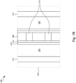
- Figure 1B illustrates a magnified top-down view of the first section 119 of Figure 1A .
- Figure 1B shows the word lines 109 separated by the gate isolation plugs 115 and the array spacers 117 separating the 3D memory array 100 from adjacent memory arrays.
- Figure 1B also shows the memory film 111 interfacing the word lines 109 and separating the semiconductor layer 113 from the word lines 109.
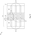
- Figure 1C illustrates a cross-sectional view of the cut-line A-A of Figure 1A , in accordance with some embodiments.
- Figure 1C illustrates a memory cell stack 120 of the 3D memory array 100, in accordance with some embodiments.
- the memory cell stack 120 comprises one of the word lines 109 operatively coupled to three of the source lines 105 and to three of the bit lines 107 via the memory film 111.
- the isolation layers 103 separate the source lines 105 from one another and the bit lines 107 from one another.
- Figure 1C further illustrates a dummy channel core 121 separating the source lines 105 from the bit lines 107.
- the semiconductor layer 113 isolates the memory film 111 from the dummy channel core 121, the source lines 105, and the bit lines 107.
- Figure 1C still further illustrates a unit memory cell 123 of the memory cell stack 120 and is highlighted with a dashed line.
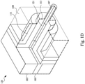
- Figure 1D illustrates in a perspective view the unit memory cell 123 of Figure 1C , in accordance with some embodiments.
- the unit memory cell 123 is illustrated in Figure 1D with a quarter section removed from its structure and with the word line 109 shown as transparent to show the interfaces between structures internal to the unit memory cell 123.
- Figure 1D illustrates the dummy channel core 121 separating the source line 105 from the bit line 107 and the semiconductor layer 113 surrounds the dummy channel core 121.
- the semiconductor layer 113 is referred to herein as a channel wrap-around structure.
- the semiconductor layer 113 also covers the vertical sidewall of the isolation layers 103 and isolates the dummy channel core 121, the source line 105 and the bit line 107 from the memory film 111.
- the memory film 111 surrounds the semiconductor layer 113 and isolates the word line 109 from the semiconductor layer 113.
- the word line 109 surrounds the memory film 111.
- the word lines 109 may be referred to herein as wrap-around electrodes.
- FIG. 1 illustrates intermediate stages in the formation of the 3D memory array 100, in accordance with some embodiments.
- FIG. 1 illustrates an embodiment of the 3D memory array 100 comprising a 3x3 memory array including three of the word lines 109, three of the source lines 105, and three of the bit lines 107.
- the memory array 100 may comprise larger sized arrays (e.g., 4x4, 5x5, 6x6, ... etc.), smaller sized arrays (e.g., 1x1, 2x2), irregular size arrays (e.g., 2x3, 2x4, 2x5, 2x6 ... 3x2, 3x4, 3x5, 3x6, ... 4x2, 4x3, 4x5, 4x6, ... etc.) and all such array sizes are within the scope of the embodiments.
- any suitable array size may be used.
- FIG. 2 illustrates forming a multi-layer stack 201 over a substrate 101, in accordance with some embodiments.
- the substrate 101 may be a semiconductor substrate, such as a bulk semiconductor, a semiconductor-on-insulator (SOI) substrate, or the like, which may be doped (e.g., with a p-type or an n-type dopant) or undoped.
- the substrate 101 may be a wafer, such as a silicon wafer.
- an SOI substrate is a layer of a semiconductor material formed on an insulator layer.
- the insulator layer may be, for example, a buried oxide (BOX) layer, a silicon oxide layer, or the like.
- the insulator layer is provided on a substrate, typically a silicon or glass substrate.
- the semiconductor material of the substrate 101 may include silicon; germanium; a compound semiconductor including silicon carbide, gallium arsenide, gallium phosphide, indium phosphide, indium arsenide, and/or indium antimonide; an alloy semiconductor including silicon-germanium, gallium arsenide phosphide, aluminum indium arsenide, aluminum gallium arsenide, gallium indium arsenide, gallium indium phosphide, and/or gallium indium arsenide phosphide; or combinations thereof.
- the multi-layer stack 201 is formed over the substrate 101.
- the multi-layer stack 201 includes alternating layers of isolation layers 103 and dummy layers 203.
- the isolation layers 103 may be referred to as "first layers of the multi-layer stack 201" and the dummy layers 203 may be referred to as "second layers of the multi-layer stack 201.”
- the isolation layers 103 and the dummy layers 203 may be dielectric materials or semiconductor materials (e.g., an oxide such as silicon oxide, SiN, Si, SiGe, or the like).
- the material of the dummy layers 203 is different from the material of the isolation layers 103.
- the isolation layers 103 may be a first material (e.g ., silicon oxide) and the dummy layers 203 may be a second material (e.g ., SiN).
- the isolation layers 103 and the dummy layers 203 may be formed using, for example, chemical vapor deposition (CVD), atomic layer deposition (ALD), physical vapor deposition (PVD), or the like.
- the multi-layer stack 201 may be formed by initially depositing a first one of the isolation layers 103 over the substrate 101.
- the isolation layers 103 may be formed by depositing a bulk layer (e.g., an oxide) using a CVD process or an ALD process.
- a bulk layer e.g., an oxide
- CVD chemical vapor deposition
- any suitable material and/or suitable deposition process may be used.
- an optional anneal process e.g ., rapid thermal anneal, oxidation densification, or the like
- an optional planarization process e.g ., chemical mechanical planarization
- the isolation layers 103 may be formed to a first height HI of between about 10 nm and about 100 nm. However, any suitable height may be used.
- a first one of the dummy layers 203 may be formed over the first one of the isolation layers 103.
- the dummy layers 203 may be formed by depositing a bulk layer (e.g., SiN) using, for example, an ALD process or a CVD process.
- a bulk layer e.g., SiN
- ALD atomic layer deposition
- CVD chemical vapor deposition
- any suitable material and/or suitable deposition process may be utilized.
- an optional anneal process e.g., a rapid thermal anneal (RTA), oxidation densification, or the like
- an optional planarization process e.g ., chemical mechanical planarization
- the dummy layers 203 may be formed to a second height H2 of between about 10 nm and about 100 nm. However, any suitable height may be used. According to some embodiments, a ratio of the first height HI of the isolation layers 103 to the second height H2 of the dummy layers 203 may be between about 0.1:1 and about 10:1. However, any suitable ratio may be utilized.
- isolation layers 103 and further dummy layers 203 may be formed in the multi-layer stack 201 in an alternating fashion one over the other until a desired topmost layer of the dummy layers 203 and a topmost layer of the isolation layers 103 have been formed.
- Any suitable number of isolation layers 103 and any suitable number of dummy layers 203 may be formed in the multi-layer stack 201. In the illustrated embodiment, four of the isolation layers 103 and three of the dummy layers 203 are formed in the multi-layer stack 201.
- Figure 2 further illustrates a first region 205 of the multi-layer stack 201.
- the first region 205 may be designated for forming the 3D memory array 100, according to some embodiments.
- a second region 207 of the multi-layer stack 201 is adjacent the first region 205 and may be designated for forming connectors to the 3D memory array 100, in accordance with some embodiments.
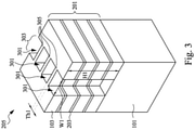
- FIG. 3 this figure illustrates the formation of gate trenches 301 within a channel region 303 of the multi-layer stack 201, according to some embodiments.
- the channel region 303 may also be referred to herein as a word line region.
- the gate trenches 301 may be formed by initially forming a photoresist (not shown) over the multi-layer stack 201.
- the photoresist may be formed using a spin-on technique and can be patterned using acceptable photolithography techniques.
- the photoresist may be patterned to expose the surface of the topmost layer of the multi-layer stack 201 in desired locations of the gate trenches 301.
- the gate trenches 301 may be patterned using one or more photolithography processes, including double-patterning or multi-patterning processes.
- double-patterning or multi-patterning processes combine photolithography and self-aligned processes, allowing patterns to be created that have, for example, pitches smaller than what is otherwise obtainable using a single, direct photolithography process.
- a sacrificial layer is formed over multi-layer stack 201 and patterned using a photolithography process. Spacers are formed alongside the patterned sacrificial layer using a self-aligned process, and the sacrificial layer may be removed.
- the spacers may be used as a mask to etch the materials of the isolation layers 103 and the materials of the dummy layers 203 exposed through the mask.
- the etching may be one or more of any acceptable etch processes, such as by wet or dry etching, a reactive ion etch (RIE), neutral beam etch (NBE), the like, or a combination thereof.
- the etching may be anisotropic.
- the mask may be used with multiple separate etching processes to remove exposed materials of the isolation layers 103 and to remove exposed materials of the dummy layers 203. However, the mask may also be used with a single etching process to etch through both of the materials of the isolation layers 103 and the dummy layers 203.
- a first etch chemical that is selective to the isolation layers 103 and relatively non-selective to the dummy layers 203 may be used to form the gate trenches 301 through the isolation layers 103 and stopping on the dummy layers 203.
- a second etch chemical that is selective to the dummy layers 203 and relatively non-selective to the isolation layers 103 may be used to form the gate trenches 301 through the dummy layers 203 and stop on the isolation layers 103.
- a single etching process may be used to remove both materials of the isolation layers 103 and the dummy layers 203, such as with an etching process that is selective to the multi-layer stack 201 ( e.g., etches the materials of the isolation layers 103 and the dummy layers 203 at a faster rate than the material of the substrate 101).
- the gate trenches 301 can be formed by a dry etch using a fluorine-based gas (e.g., C 4 F 6 ) mixed with hydrogen (H 2 ) or oxygen (O 2 ) gas.
- a fluorine-based gas e.g., C 4 F 6
- hydrogen H 2
- oxygen O 2
- timed etch processes may be used to stop the etching of the gate trenches 301 after the trenches have reach a desired depth.
- the timed etch process may be timed to stop at the surface of the substrate 101, although the timed etch process may be timed to etch into the substrate 101 to a desired depth.
- an optional contact etch stop layer (not shown) may be provided at an interface between the substrate 101 and the multi-layer stack 201.
- the optional contact etch stop layer may comprise a dielectric material, such as, silicon nitride, silicon oxide, silicon oxynitride, or the like, having a different etch rate than the materials of an overlying layer of the multi-layer stack 201.
- the optional contact etch stop layer is formed via a suitable deposition process (e.g ., atomic layer deposition, chemical vapor deposition, physical vapor deposition, or the like) over the substrate 101 prior to the formation of the multi-layer stack 201 and the multi-layer stack 201 is formed over the optional contact etch stop layer.
- a suitable deposition process e.g ., atomic layer deposition, chemical vapor deposition, physical vapor deposition, or the like
- an additional etch process may be used to remove materials of the optional contact etch stop layer such that the substrate 101 is exposed at the bottom of the gate trenches 301.
- the gate trenches 301 are separated by the fins 305.
- the gate trenches 301 may be formed to a first width W1 of between about 50 nm and about 500 nm and a first height HI of between about 500 nm and about 5,000 nm and the fins 305 may be formed to a first thickness Th1 of between about 5 nm and about 30 nm.
- any suitable width, height and thickness may be used.
- the gate trenches 301 are formed to an aspect ratio of between about 10:1 and about 50:1, in accordance with some embodiments. However, any suitable aspect ratio may be used.
- widths of the fins 305 of the memory array 100 located in one region of the multi-layer stack 201 may be greater or thinner than the fins 305 of another memory array 100 located in another region of the multi-layer stack 201.
- each of the gate trenches 301 are illustrated as having a consistent width throughout, according to some embodiments.
- the gate trenches 301 and thus the fins 305 may have tapered sidewalls such that a width of each of the fins 305 continuously increases in a direction towards the substrate 101.
- each of the isolation layers 103 and the dummy layers 203 may have a different width in a direction perpendicular to the sidewalls of the fins 305.
- Figure 4 illustrates a wire-release process for forming 401 from the dummy layers 203.
- the spacers and/or photoresist used to form the gate trenches 301 in Figure 3 may be removed and a mask layer (not shown) for use in the wire-release process may be formed over the multi-layer stack 201 and patterned to expose the channel region 303.
- the spacers and/or photoresist layer used to form the gate trenches 301 may be retained and the mask layer for use in the wire-release process is formed over the spacers and the photoresist layer.
- the mask layer may be formed over the photoresist and/or the spacers and then patterned to expose the portions of the photoresist and/or the spacers covering the gate trenches 301 and/or the fins 305 in the channel region.
- the mask layer may be a conductive or non-conductive material and may be selected from a group including silicon nitride, silicon oxynitride, amorphous silicon, polycrystalline-silicon (polysilicon), poly-crystalline silicon-germanium (poly-SiGe), metallic nitrides, metallic silicides, metallic oxides, and metals.
- the mask layer may be deposited by physical vapor deposition (PVD), CVD, ALD, sputter deposition, or other techniques for depositing the selected material. Once the material of the mask layer has been deposited, the material may be patterned using, e.g., a photolithographic masking and etching process. Once the mask layer is patterned, the exposed portions of the photoresist and/or the spacers are removed using one or more suitable removal processes (e.g., ashing, selective etching, combinations, or the like).
- the sidewalls of the gate trenches 301 and thus the sidewalls of the fins 305 are exposed.
- the material of the isolation layers 103 of the fins 305 may be removed from between the substrate 101 and the dummy layers 203 in a wire release process step.
- the remaining material of fins 305 e.g., the dummy layers 203 form an array of dummy nanostructures 401 between source/bit line regions 403 of the multi-layer stack 201.
- the wire release process step may also be referred to as a sheet release process step, a sheet formation process step, a nanosheet formation process step or a wire formation process step.
- the dummy nanostructures 401 may be referred to herein as dummy wires, dummy nanowires, dummy sheets, or dummy nanosheets.
- the isolation layers 103 of the fins 305 may be removed using a wet etching process that selectively removes the material of the isolation layers 103 (e.g., silicon oxide) without significantly removing the materials of the substrate 101 and the material of the dummy nanostructures 401 (e.g., silicon nitride (SiN)) within the channel region 303 and without significantly removing the materials of the isolation layers 103 and the material of the dummy layers 203 (e.g., silicon nitride (SiN)) of the source/bit line regions 403 of the multi-layer stack 201.
- any suitable removal process may be utilized.
- an etch chemical containing phosphorous may be used to selectively remove the material of the isolation layers 103 (e.g., OX) without substantively removing the material of the dummy nanostructures 401 ( e.g., SiN) and/or the material of the substrate 101 ( e.g., SiC).
- the wet etching process may be performed at a temperature of between about 20°C and about 150°C, and for a time of between about 10 seconds and about 300 seconds.
- any suitable etchant, process parameters, and time can be utilized.
- the sides of the dummy nanostructures 401 are exposed and separated from each other within the channel region 303.
- the dummy nanostructures 401 are separated by a first spacing S1 of between about 5nm and about 15nm.
- a first spacing S1 of between about 5nm and about 15nm.
- the dummy nanostructures 401 form a dummy channel structure between opposite ones of the source/bit line regions 403 and have a channel length (CL) of between about 5nm and about 180nm.
- the dummy nanostructures 401 may be formed to have a channel width (CW) of between about 8nm and about 100nm.
- a tuning selectivity of the etching process may be adjusted such that the dummy nanostructures 401 are formed with smooth surfaces or facet-limited surfaces.
- the dummy nanostructures 401 may be formed with different profile shapes (e.g ., round, square, rectangle, hexagon, octagon, or the like).
- the dummy nanostructures 401 are formed to have a round profile with the channel width CW being about the same as the original thicknesses of the dummy layers 203 such as, of between about 3nm and about 15nm, although the etching processes may also be utilized to reduce the thicknesses.
- any remaining portions of the mask layer, the retained spacers and/or the retained photoresist may be removed using one or more suitable removal processes (e.g ., wet etch, dry etch, or the like) that utilize one or more etchants that are selective to the materials of the mask layer, the retained spacers and/or the retained photoresist.
- suitable removal processes e.g ., wet etch, dry etch, or the like
- any suitable removal process may be utilized.
- this figure illustrates the formation of the semiconductor layer 113.
- the semiconductor layer 113 is formed as a conformal thin film of an acceptable semiconductor material for providing wrap-around channel regions over the exposed surfaces of the dummy nanostructures 401 and along sidewalls and top surfaces of the source/bit line regions 403. As such, the semiconductor layer 113 wraps around and adopts the profile shape ( e.g ., round) of the dummy nanostructures 401.
- the semiconductor layer 113 may be a thin film layer of material such as zinc oxide (ZnO), indium gallium zinc oxide (IGZO), indium tungsten oxide (IWO), indium tin oxide (ITO), indium gallium zinc tin oxide (IGZTO), other metal oxides, polysilicon, amorphous silicon, or the like.
- a thickness of the semiconductor layer 113 can be between about 5 nm and about 20 nm. However, any suitable thickness may be used.
- the semiconductor layer 113 may be formed by an acceptable deposition process such as ALD, CVD, PVD, or the like. However, any suitable materials and deposition processes may be utilized to form the semiconductor layer 113.
- the memory film 111 is formed as a conformal thin film over the exposed surfaces of the semiconductor layer 113.
- the memory film 111 may be formed using one or more layers of acceptable dielectric materials suitable for storing digital values, such as multilayer dielectrics (e.g ., oxide-nitride-oxide (ONO), nitride-oxide-nitride (NON), or the like); other dielectrics ( e.g ., silicon oxynitride (SiON), silicon nitride (SiN), or the like); ferro-electric (FE) materials such as, hafnium zirconium oxide (HfZrO); zirconium oxide (ZrO); undoped hafnium oxide (HfO); doped hafnium oxides (e.g ., HfLaO using lanthanum (La) as a dopant
- multilayer dielectrics e.g ., oxide-nitride-oxide (ONO), nitride
- a thickness of the memory film 111 can be in the range of about 5 nm to about 30 nm.
- the material of the memory film 111 may be formed by an acceptable deposition process such as atomic layer deposition, chemical vapor deposition, physical vapor deposition, or the like.
- Figure 7 illustrates the formation of a wrap-around word line structure 701 formed over the memory film 111 and a subsequent chemical mechanical planarization.
- the wrap-around word line structure 701 may comprise one or more layers, such as glue layers, barrier layers, diffusion layers, and fill layers, and the like.
- the wrap-around word line structure 701 may be referred to herein as a conductive wrap-around structure, a word line stack, or a word line electrode.
- the wrap-around word line structure 701 includes a glue layer and a conductive layer.
- the glue layer may be formed of metal nitride, such as titanium nitride, tantalum nitride, zirconium nitride, hafnium nitride, or the like.
- the conductive layer may be formed of a metal such as tungsten, cobalt, aluminum, nickel, copper, silver, gold, alloys thereof, or the like.
- the material of the glue layer is one that has good adhesion to the material of the memory film 111 and the material of the conductive layer is one that has good adhesion to the material of the glue layer.
- the glue layer can be titanium nitride and the conductive layer can be tungsten.
- the glue layer and conductive layer may each be formed by an acceptable deposition process such as atomic layer deposition (ALD), chemical vapor deposition (CVD), or the like.
- the materials of the wrap-around word line structure 701 may fill and overfill the remaining opening in the channel region 303 and may be formed over the top surfaces of the memory film 111 outside of the channel region 303.
- the glue layer can have a thickness in the range of about 1 nm to about 10 nm.
- the conductive layer fills the remaining area of the gate trenches 301 and can have a thickness in the range of about 15 nm to about 200 nm.
- the wrap-around word line structure 701 may be formed with a second height H2 of between about 500 nm and about 5,000 nm and a second width W2 of between about 30 nm and about 400 nm. However, any suitable height and width may be used.
- the wrap-around word line structure 701 may be formed with a first length L1 of between about 1,000 nm and about 100,000 nm.
- the aspect ratio (AR) of the wrap-around word line structure 701 is the ratio of the second height H2 to the second width W2.
- the wrap-around word line structure 701 is formed with an aspect ratio between about 2.5:1 and about 200:1. However, any suitable aspect ratios may be used to form the wrap-around word line structure 701.
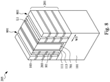
- Figure 8 illustrates the formation of array slits 801 in the multi-layer stack 201.
- the array slits 801 may be referred to herein as vertical slits, vertical trenches, or vertical array openings.
- the array slits 801 extend through the multi-layer stack 201 and expose the substrate 101.
- the array slits 801 extend through some but not all layers of the multi-layer stack 201.
- the array slits 801 may be formed using any of the photolithography and anisotropic etching techniques suitable for forming the gate trenches 301, as set forth above. However, other suitable photolithography and etching techniques may also be used to form the array slits 801.
- Forming the array slits 801 divides the multi-layer stack 201 and separates one region of the multi-layer stack 201 occupied by the intermediate structure of the 3D memory array 100 from adjacent regions of the multi-layer stack 201.
- the adjacent regions of the multi-layer stack 201 may also be occupied by intermediate structures similar to that of the 3D memory array 100, although other structures may be also be formed in one or more of the adjacent regions.
- the array slits 801 may be formed with a third width W3 of between about 20 nm and about 200 nm.
- the array slits 801 may be formed with a first length L1 of between about 1,000 nm and about 100,000 nm.
- the aspect ratio (AR) of each of the array slits 801 is the ratio of the first height HI to the third width W3.
- the array slits 801 may be formed to have a same aspect ratio, although the array slits 801 may be formed to different aspect ratios.
- the array slits 801 are formed with an aspect ratio between about 50:1 and about 100:1.
- any suitable aspect ratios may be used to form the array slits 801.
- FIGS 9A and 9B these figures illustrate the formation of source/bit line gaps 901 in the multi-layer stack 201.
- the source/bit line gaps 901 may be formed by any acceptable etching process, such as one that is selective to the material of the dummy layers 203 ( e.g ., selectively etches the material of the dummy layers 203 at a faster rate than the materials of the isolation layers 103, the semiconductor layer 113 and the substrate 101).
- the source/bit line gaps 901 can be formed by a wet etch using an etch chemical comprising an acid and an oxidizer.
- the etch chemical used may be a mixture of hydrochloric acid (HCl) and hydrogen peroxide (H 2 O 2 ), where HCl functions as the acid and H 2 O 2 functions as the oxidizer.
- a mixing ratio (e.g ., volume ratio) between HCl and H 2 O 2 is between about 1:1 and 1:20 for the wet etch process.
- the wet etch process may be performed at a temperature between about 40 °C and about 70 °C for a duration between about 1 minute and about 5 minutes, or else may be ended using an endpoint detection process.
- Figure 9A further illustrates an area 907 of one of the array slits 801.
- the area 907 is highlighted with a dashed line and the area 907 is also illustrated in a magnified view in Figure 9A .
- a sidewall of the semiconductor layer 113 can be seen through one of the source/bit line gaps 901 in between two of the isolation layers 103.
- a recess 905 in the dummy nanostructure 401 from the sidewall of the semiconductor layer 113 is also illustrated in the magnified view of the area 907 of Figure 9A .
- the dummy nanostructures 401 may be recessed from the sidewall of the semiconductor layer 113 in a timed process of the removal of the dummy layers 203.
- the dummy nanostructures 401 may be recessed in a subsequent etching step using an etch chemical that is selective to the material of the dummy nanostructures 401 and non-selective to the materials of the semiconductor layer 113 and the substrate 101.
- Figure 9B is a top-down view of a cross section taken through the dummy nanostructure 401 (relabeled dummy channel core 121 in Figure 9B).
- Figure 9B illustrates the isolation layers 103 in phantom to indicate that the level of the isolation layers 103 are below a level of the dummy channel core 121.
- Figure 9B illustrates the semiconductor layer 113 between two of the source/bit line gaps 901, the semiconductor layer 113 surrounding and being wrapped around the dummy nanostructure 401, the memory film 111 over and surrounding the semiconductor layer 113 and the wrap-around word line structure 701 over and surrounding the memory film 111.
- Figure 9B further illustrates the recesses 905 in the dummy channel core 121.
- the etching process is a timed process used to form the recesses 905 in the dummy material of the dummy channel core 121 to a first depth D1.
- the first depth D1 may be between about 1 nm and about 20 nm.
- any suitable depth may be used.
- a tuning selectivity of the etching process may be adjusted to shape the distal ends of the dummy channel core 121 to a desired shape (e.g ., concave, convex, flat, round, facet-limited, or the like). In the illustrated embodiment, the distal ends of the dummy channel core 121 are concave.
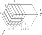
- this figure illustrates the formation of a metal fill material 1001 in the array slits 801 ( see, e.g., Figure 8 ) and the source/bit line gaps 901 ( see, e.g., Figure 9 ).
- the metal fill material 1001 may comprise one or more layers, such as glue layers, barrier layers, diffusion layers, and fill layers, and the like and may be formed using any of the materials and processes suitable for forming the wrap-around word line structure 701.
- the materials used to form the metal fill material 1001 may be the same as the materials used to form the wrap-around word line structure 701, although they may be different.
- the metal fill material 1001 includes a glue layer and a conductive layer.
- the glue layer may be formed of a metal nitride suitable for forming the wrap-around word line structure 701 (e.g ., titanium nitride, tantalum nitride, zirconium nitride, hafnium nitride, or the like).
- the conductive layer may be formed of a metal suitable for forming the wrap-around word line structure 701 ( e.g ., tungsten (W), titanium (Ti), titanium nitride (TiN), tantalum nitride (TaN), or the like).
- the material of the glue layer is one that has good adhesion to the material of the isolation layers 103 and/or the semiconductor layer 113 and the material of the conductive layer is one that has good adhesion to the material of the glue layer.
- the glue layer can be formed of titanium nitride (TiN) and the conductive layer can be formed of tungsten (W).
- TiN titanium nitride
- W tungsten
- the glue layer and conductive layer may each be formed by an acceptable deposition process such as atomic layer deposition, chemical vapor deposition, or the like.
- the materials of the metal fill material 1001 may be formed to fill and overfill the array slits 801 and the source/bit line gaps 901 and may be formed over the top surfaces of the topmost layers of the isolation layers 103 outside of the array slits 801.
- the glue layer can have a thickness in the range of about 1 nm to about 10 nm.
- the materials of the metal fill material 1001 may be planarized with the topmost layers of the isolation layers 103, the memory film 111 and the semiconductor layer 113, and the wrap-around word line structure 701 using a process such as chemical mechanical planarization.
- FIG. 11 this figure illustrates a formation of word line gaps 1101 and removal of the metal fill material 1001 from within the array slits 801 according to some embodiments.
- the word line gaps 1101 may be formed using any of the photolithography and etching techniques suitable for etching the materials of the wrap-around word line structure 701. The etching may be anisotropic.
- the conductive layer of the wrap-around word line structure 701 is tungsten (W) and the glue layer of the wrap-around word line structure 701 is titanium nitride (TiN)
- the memory film 111 is an oxide-nitride-oxide (ONO) film and the semiconductor layer 113 is zinc oxide (ZnO)
- the word line gaps 1101 can be formed and the array slits 801 can be re-exposed by a series of appropriate etches (e.g., dry etches and/or wet etches).
- a dry etch is performed using a fluorine-based gas (e.g., C 4 F 6 ) mixed with hydrogen (H 2 ) or oxygen (O 2 ) gas is used to remove the conductive layer of the wrap-around word line structure 701 and a wet etch is performed using a nitric acid (HNO 3 ) and hydrofluoric acid (HF) solution to remove the glue layer of the wrap-around word line structure 701.
- a fluorine-based gas e.g., C 4 F 6
- hydrogen (H 2 ) or oxygen (O 2 ) gas is used to remove the conductive layer of the wrap-around word line structure 701
- a wet etch is performed using a nitric acid (HNO 3 ) and hydrofluoric acid (HF) solution to remove the glue layer of the wrap-around word line structure 701.
- HNO 3 nitric acid
- HF hydrofluoric acid
- other suitable removal processes may be utilized to remove the materials from the word line gaps 1101 and to
- the word lines 109 may be formed with a second length L2, the second width W2, and the first height HI. According to some embodiments, the second length L2 may be a distance of between about 30 nm and about 100 nm. In some embodiments, the array slits 801 may be formed with a first length L1 of between about 1,000 nm and about 100,000 nm. However, any suitable dimensions may be utilized.
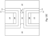
- Figures 12A-12C illustrate the formation of the array spacers 117, the gate isolation plugs 115, the source lines 105, the bit lines 107, and the word lines 109 according to some embodiments.
- Figure 12A illustrates the 3D memory array 100 in a perspective view with the gate isolation plugs 115 and the array spacers 117 formed in the word line gaps 1101 and the array slits 801 of Figure 11 .
- Figure 12B illustrates the 3D memory array 100 in another perspective view with the source lines 105, the bit lines 107, the gate isolation plugs 115 and the array spacers 117 illustrated in phantom view to show the interface between the semiconductor layer 113 and the gate isolation plugs 115 internal to the 3D memory array 100.
- Figure 12B further illustrates a magnified view of a second area 1201 to show details of the interface.
- Figure 12C illustrates a top down view of the cross-section taken through the dummy channel core 121.
- the array spacers 117 and the gate isolation plugs 115 are formed of dielectric materials. Acceptable dielectric materials include, but are not limited to oxides such as silicon oxide; nitrides such as silicon nitride; carbides such as silicon carbide; the like; or combinations thereof such as silicon oxynitride, silicon oxycarbide, silicon carbonitride, or the like.
- the array spacers 117 and the gate isolation plugs 115 are formed using the same materials and a same deposition process.
- the gate isolation plugs 115 may be formed to the first thickness Th1, the second width W2, and the first height HI.
- the material of the gate isolation plugs 115 and the array spacers 117 may be formed by an acceptable deposition process such as ALD, CVD, flowable CVD (FCVD), or the like to fill and/or overfill the word line gaps 1101 and array slits 801, respectively.
- an acceptable deposition process such as ALD, CVD, flowable CVD (FCVD), or the like to fill and/or overfill the word line gaps 1101 and array slits 801, respectively.
- the materials used to form the gate isolation plugs 115 may be different from the materials used to form the array spacers 117.
- separate removal processes may be used to re-expose the array slits 801 and to form the word line gaps 1101.
- separate deposition processes may be used to form the gate isolation plugs 115 and the array spacers 117.
- the array spacers 117 may be formed before the gate isolation plugs 115, although the array spacers 117 may be formed after the gate isolation plugs 115. All such removal processes, deposition processes, and ordering of such processes are within the scope of the embodiments.
- Figure 13 illustrates a first 3D-NOR memory device 1300, according to some embodiments.
- the first 3D-NOR memory device 1300 comprises a staircase contact structure 1313 formed within the second region 207 of the multi-layer stack 201 adjacent the 3D memory array 100 in accordance with some embodiments.
- the staircase contact structure 1313 may be formed by initially placing a photoresist (not shown) over the multi-layer stack 201.
- the photoresist can be formed by using a spin-on technique and can be patterned using acceptable photolithography techniques. Patterning the photoresist may expose a portion of the multi-layer stack 201 in a first staircase region 1301 while masking remaining portions of the multi-layer stack 201.
- the exposed portions of the multi-layer stack 201 in the first staircase region 1301 are etched in a staircase etching process using the photoresist as a mask.
- the staircase etching process may be any acceptable etch process, such as by wet or dry etching, a reactive ion etch (RIE), neutral beam etch (NBE), the like, or a combination thereof.
- the etching may be anisotropic.
- the etching may remove portions of the topmost layers of the isolation layers 103 and the dummy layers 203 in the first staircase region 1301 such that the isolation layer 103 underlying the topmost layer of the dummy layers 203 is exposed in the first staircase region 1301.
- the dummy layers 203 act as etch stop layers while etching the overlying layer of the isolation layers 103.
- the topmost layers of the dummy layers 203 are exposed in the first staircase region 1301.
- the underlying isolation layers 103 act as etch stop layers while etching the overlying layer of the dummy layers 203.
- the portions of the topmost layers of the isolation layers 103 and the dummy layers 203 may be selectively removed without removing remaining layers of the multi-layer stack 201, and the pattern of the photoresist may be extended into the first staircase region 1301 of the multi-layer stack 201 to a desired depth.
- a timed etch processes may be used to stop the etching after reach a desired depth into first staircase region 1301 of the multi-layer stack 201.
- the next layer of the isolation layers 103 underlying the topmost layer of the dummy layers 203 is exposed in the first staircase region 1301.
- the photoresist may be trimmed to expose another portion of the multi-layer stack 201 in a second staircase region 1303 while masking remaining portions of the multi-layer stack 201 outside of the first staircase region 1301 and the second staircase region 1303.
- the exposed portions of the multi-layer stack 201 in the first staircase region 1301 and second staircase region 1303 are etched by repeating the staircase etching process using the trimmed photoresist as a mask.
- the etching may remove portions of the topmost layers of the isolation layers 103 and the dummy layers 203 exposed in the second staircase region 1303 and in the first staircase region 1301 such that the next layer down of the isolation layers 103 in the multi-layer stack 201 is exposed in each of the first staircase region 1301 and the second staircase region 1303.
- the photoresist may be trimmed again to expose yet another portion of the multi-layer stack 201 in a third staircase region 1305 while masking remaining portions of the multi-layer stack 201.
- the trimming of the photoresist and the staircase etching process may be repeated until a desired number of staircase regions have been exposed. In the illustrated embodiment, three of the staircase regions are exposed with the last trimming of the photoresist exposing the third staircase region 1305. However, more of fewer staircase regions may be formed.
- a multi-layer stack 201 comprising a lesser number of source lines 105 or bit lines 107 ( e.g., two), fewer staircase regions (e.g., two) may be formed.
- a multi-layer stack 201 comprising a greater number of source lines 105 or bit lines 107 ( e.g., four, five, six, ... etc.)
- more staircase regions e.g., four, five, six, ... etc.
- staircase contact areas 1307 are exposed by using the trimmed photoresist as a mask and etching the exposed portions of the isolation layers 103 in the staircase regions.
- the etching may remove portions of the topmost layers of the isolation layers 103 such that the next layer down of the metal fill material 1001 in the multi-layer stack 201 are exposed in each of the first staircase region 1301, the second staircase region 1303, and the third staircase region 1305.
- These exposed portions of the metal fill material 1001 may serve as the staircase contact areas 1307.
- Figure 13 further illustrates a formation of conductive contacts 1309 over the staircase contact areas 1307 and the word lines 109, according to some embodiments.
- the conductive contacts 1309, the staircase contact areas 1307 and isolation layers 103 adjacent the memory array 100 may be collectively referred to as a staircase contact structure 1313.
- the staircase contact structures 1313 of arrays adjacent to the 3D memory array 100 may be separated by the third width W3 of the array spacers 117.
- the conductive contacts 1309 provide external connectivity to the word lines, source lines 105 and bit lines 107 of the 3D memory array 100.
- the conductive contacts 1309 may electrically connect the 3D memory array 100 to other active devices and/or signal, power, and ground lines in a semiconductor die. Accordingly, the first 3D-NOR memory device 1300 may be completed.
- the conductive contacts 1309 may be formed by initially forming an interlayer dielectric (ILD) layer (not shown) over the first region 205 and the second region 207 of the multi-layer stack 201. Once formed, the interlayer dielectric layer is patterned using suitable photolithographic and etching processes to form openings through the interlayer dielectric layer and expose areas of the word lines 109 and/or the staircase contact areas 1307 in desired locations of the conductive contacts 1309.
- ILD interlayer dielectric
- the openings may be filled and/or overfilled with a conductive fill material (e.g ., W, Al, Cu, or the like) using a suitable deposition process (e.g ., chemical vapor deposition (CVD), physical vapor deposition (PVD), or the like).
- a planarization process may be performed to planarize the top surfaces of the conductive contacts 1309 to be co-planar with a surface of the interlayer dielectric layer.
- the interlayer dielectric layer (not shown) may remain to allow for further processing of the first 3D-NOR memory device 1300, according to some embodiments.
- the embodiment of Figure 13 illustrates a particular pattern for the staircase contact structures 1313, other configurations are also possible.
- the source lines 105 and the bit lines 107 that are in a same row of the array are all aligned with each other and the staircase contact areas 1307 of the bit lines 107 are formed on a same side of the 3D memory array 100 as the source lines 105.
- the staircase contact areas 1307 of bit lines 107 may be formed on a side of the 3D memory array 100 opposite from the staircase contact areas 1307 of source lines 105.
- the word lines 109 of an adjacent memory array may be aligned with the word lines 109 of the 3D memory array 100, although the word lines 109 of one memory array may also be offset from the word lines 109 of an adjacent memory array such that the word lines 109 and thus the conductive contacts 1309 connected to the word lines 109 have a staggered pattern from one memory array to the next memory array.
- Figures 14A illustrates a top-down view of a second 3D-NOR memory device 1400, according to some embodiments.
- the second 3D-NOR memory device 1400 comprises a plurality of second 3D-memory arrays 1403 and a plurality of the staircase contact structures 1313.
- Each of the second 3D-memory arrays 1403 comprises four of the word lines 109 and a pair of the staircase contact structures 1313.
- Each pair of the staircase contact structures 1313 are associated with three staircase contact areas 1307 of the source lines 105 and three staircase contact areas 1307 of the three bit lines 107.
- the staircase contact areas 1307 are designated in Figure 14 as being associated with a stack of source lines 105 (e.g., SL1, SL2, SL3) and one of the second 3D-memory arrays 1403 being associated with a stack of bit lines 107 ( e.g., BL1, BL2, BL3) and one of the second 3D-memory arrays 1403.
- source lines 105 e.g., SL1, SL2, SL3
- bit lines 107 e.g., BL1, BL2, BL3
- each of a plurality of conductive source line structures 1407 are connected to the conductive contacts 1309 of the source lines 105, respectively for external connection to the second 3D-NOR memory device 1400 and each of a plurality of conductive bit line structures 1409 are connected to the conductive contacts 1309 of the bit lines 107, respectively for external connection to the second 3D-NOR memory device 1400.
- one or more of the conductive contacts 1309 of the source lines 105 may be connected to one of the conductive source line structures 1407 for external connection to the second 3D-NOR memory device 1400 and/or one or more of the conductive contacts 1309 of the bit lines 107 may be connected to one of the conductive bit line structures 1409 for external connection to the second 3D-NOR memory device 1400.
- Figure 14A further illustrates a unit memory cell 123 of one of the second 3D-memory arrays 1403 highlighted with a dashed line.
- the word lines 109 of adjacent ones of the second 3D-memory arrays 1403 are aligned with one another.
- the word lines 109 of adjacent ones of the second 3D-memory arrays 1403 may be offset from one another having a staggered pattern from one memory array to the next memory array.
- conductive word line structures 1405 may be formed to the conductive contacts 1309 to externally connect the word lines 109 of the second 3D-memory arrays 1403 to external devices.
- the word lines 109 of adjacent ones of the second 3D-memory arrays 1403 are electrically connected to one another by one of the conductive word line structures 1405 and are designated ( e.g ., WL1, WL2, WL3, WL4) as being associated with a set of word lines 109 that are connected.
- the conductive word line structures 1405 may connect the word lines 109 that are aligned with other word lines 109 of the staggered arrangement one to another within the second 3D-memory arrays 1403.
- Figure 14B is a schematic diagram of an equivalent circuit 1410 of the second 3D-NOR memory device 1400 illustrated in the Figure 14A .
- Figure 14B illustrates three columns 1411 of four of the circuit elements 1413 representing the second 3D-memory arrays 1403 with the conductive word line structures 1405 associated with sets of the word lines 109 of the second 3D-memory arrays 1403 and are designated ( e.g ., WL1, WL2, WL3, WL4).
- Figure 14B further illustrates the conductive source line structures 1407 associated with the stack of source lines 105 (e.g., SL1, SL2, SL3) of the second 3D-memory arrays 1403 and the conductive bit line structures 1409 associated with the stack of bit lines 107 ( e.g., BL1, BL2, BL3) of the second 3D-memory arrays 1403.
- Figure 14B further illustrates the circuit element 1413 of the equivalent circuit 1450 associated with the unit memory cell 123 highlighted with the dashed line in Figure 14A .
- Various embodiments provide a 3D-NOR memory array 100 with a plurality of vertically stacked memory cells 125 which provide one or more of the following advantages and/or benefits. For example, by forming the 3D-NOR memory array 100 as described above, the manufacturing production of a large array of devices can be simplified and material costs savings can be achieved. Additionally, with the isolation layers 103 separating the source lines 105 and bit lines 107, disturbances in read/write operations of the 3D-NOR memory array 100 are reduced. As such, production yield and device performance are increased.
- a method includes: forming a multi-layer stack over a substrate, the multi-layer stack including alternating layers of an isolation material and a dummy material; forming an array of dummy nanostructures in a channel region of the multi-layer stack; depositing a semiconductor material surrounding the array of dummy nanostructures; depositing a memory film over the semiconductor material; and forming a conductive structure around the memory film.
- forming the multi-layer stack includes using a first material for the isolation material and using a second material for the dummy material, the second material being different from the first material.
- the method further includes forming source/bit line structures by replacing the dummy material located outside of the channel region with a conductive material.
- the method further includes forming a staircase contact structure from the source/bit line structures outside of the channel region.
- forming the source/bit line structures further includes forming recesses within the dummy nanostructures.
- the method further includes filling the recesses with the conductive material.
- the method further includes: etching an opening through the conductive structure, the memory film, and the semiconductor material in a location between adjacent stacks of the array of dummy nanostructures; and depositing a dielectric material in the opening.
- a method in another embodiment, includes: depositing a first material over a substrate; forming a multi-layer stack by depositing a second material over the first material; forming a fin in a channel region of the multi-layer stack; forming a dummy channel core by removing the first material from the fin; depositing a semiconductor material over and surrounding the dummy channel core; depositing a memory film layer over the semiconductor material; forming a conductive structure over the memory film layer; and replacing remaining portions of the second material located outside of the channel region with a conductive material.
- depositing the semiconductor material deposits an oxide material.
- the oxide material is indium gallium zinc oxide.
- replacing the remaining portions of the second material includes forming slits in the multi-layer stack on opposite sides of the dummy channel core. In an embodiment, replacing the remaining portions of the second material further includes etching the second material exposed along sidewalls of the slits. In an embodiment, replacing the remaining portions of the second material further includes forming recesses within the dummy channel core. In an embodiment, the method further includes forming a staircase contact structure in electrical connection with the conductive material. In an embodiment of the method, depositing the memory film layer includes depositing a ferroelectric material.
- a device in yet another embodiment, includes: a memory cell stack including a stack of dummy nanostructure cores; a semiconductor wrap-around channel structure surrounding each one of the dummy nanostructure cores; a memory film surrounding the semiconductor wrap-around channel structure; and a wrap-around word line surrounding the semiconductor wrap-around channel structure.
- the device further includes a stack of source line structures and a stack of bit line structures, each bit line structure within the stack of bit line structures being separated from a corresponding one of the source line structures within the stack of source line structures by a corresponding one of the dummy nanostructure cores within the stack of dummy nanostructure cores.
- the stack of source line structures and the stack of bit line structures are separated from the wrap-around word line by the semiconductor wrap-around channel structure.
- the device further includes a stack of isolation regions, wherein the source line structures are isolated from one another by the stack of isolation regions.
- the semiconductor wrap-around channel structure is an oxide semiconductor film.
Landscapes
- Semiconductor Memories (AREA)
- Chemical & Material Sciences (AREA)
- Engineering & Computer Science (AREA)
- Nanotechnology (AREA)
- Non-Volatile Memory (AREA)
Abstract
Description
- Semiconductor devices are used in a variety of electronic applications, such as, for example, personal computers, cell phones, digital cameras, and other electronic equipment. Semiconductor devices are typically fabricated by sequentially depositing insulating or dielectric layers, conductive layers, and semiconductor layers of material over a semiconductor substrate, and patterning the various material layers using lithography to form circuit components and elements thereon.
- The semiconductor industry continues to improve the integration density of various electronic components (e.g., transistors, diodes, resistors, capacitors, etc.) by continual reductions in minimum feature size, which allow more components to be integrated into a given area.
- Aspects of the present disclosure are best understood from the following detailed description when read with the accompanying figures. It is noted that, in accordance with the standard practice in the industry, various features are not drawn to scale. In fact, the dimensions of the various features may be arbitrarily increased or reduced for clarity of discussion.
-
Figures 1A-1D illustrate a 3D NOR memory array, in accordance with some embodiments. -
Figures 2-12C illustrate intermediate stages in the formation of the 3D NOR memory array, in accordance with some embodiments. -
Figure 13 illustrates a 3D NOR memory device with a staircase contact structure for external connection to the 3D NOR memory array, according to some embodiments. -
Figures 14A illustrates a top-down view of another 3D NOR memory device, according to some embodiments. -
Figure 14B illustrates a schematic diagram of an equivalent circuit of the 3D NOR memory device illustrated inFigure 14A . - The following disclosure provides many different embodiments, or examples, for implementing different features of the invention. Specific examples of components and arrangements are described below to simplify the present disclosure. These are, of course, merely examples and are not intended to be limiting. For example, the formation of a first feature over or on a second feature in the description that follows may include embodiments in which the first and second features are formed in direct contact, and may also include embodiments in which additional features may be formed between the first and second features, such that the first and second features may not be in direct contact. In addition, the present disclosure may repeat reference numerals and/or letters in the various examples. This repetition is for the purpose of simplicity and clarity and does not in itself dictate a relationship between the various embodiments and/or configurations discussed.
- Further, spatially relative terms, such as "beneath," "below," "lower," "above," "upper" and the like, may be used herein for ease of description to describe one element or feature's relationship to another element(s) or feature(s) as illustrated in the figures. The spatially relative terms are intended to encompass different orientations of the device in use or operation in addition to the orientation depicted in the figures. The apparatus may be otherwise oriented (rotated 90 degrees or at other orientations) and the spatially relative descriptors used herein may likewise be interpreted accordingly.
- Embodiments will now be described with respect to a particular embodiment which forms a 3-dimensional (3D) memory array includes a plurality of NOR gate-all-around (GAA) stacked memory cells. However, the embodiments described are intended to be illustrative and are not intended to be limited to those embodiments that are expressly described herein. Rather, the ideas presented herein may be incorporated into a wide variety of embodiments.
- With reference now to
Figures 1A-1D , these figures illustrate an example of a3D memory array 100, in accordance with some embodiments. The3D memory array 100 may be a NOR gate-all-around (GAA) memory array. In the illustrated embodiment, the3D memory array 100 is formed as a 3x3 matrix of vertically stackedmemory cells 125. However, other embodiments of the3D memory array 100 may comprise more memory cells or fewer memory cells and all such memory arrays are within the scope of the present disclosure. - In particular,
Figure 1A illustrates in a perspective view the3D memory array 100 over asubstrate 101, according to some embodiments. The3D memory array 100 comprisesisolation layers 103separating source lines 105 andbit lines 107 of a plurality of vertically stackedmemory cells 125. Thesource lines 105 andbit lines 107 may be referred to herein as source line structures, bit line structures, source/bit lines, or source/bit line structures. -
Figure 1A further illustratesword lines 109 of the vertically stackedmemory cells 125 that are separated from thesource lines 105 and thebit lines 107 via ansemiconductor layer 113 and amemory film 111 internally within the3D memory array 100. Theword lines 109 may be referred to herein as word line structures. - The
semiconductor layer 113 is isolated from theword lines 109 by thememory film 111. Thesemiconductor layer 113 may be referred to herein as a channel wrap-around structure, an oxide wrap-around layer, an oxide channel wrap-around structure, an oxide semiconductor structure, or an oxide wrap-around structure. Further still,Figure 1A illustratesgate isolation plugs 115 that separate theword lines 109 of the stacked memory cells from one another andarray spacers 117 separating the3D memory array 100 from adjacent memory arrays.Figure 1A further illustrates afirst section 119 highlighted by a dashed line and a cross-section A-A which will be referenced with regard to the following discussion and figures. -
Figure 1B illustrates a magnified top-down view of thefirst section 119 ofFigure 1A .Figure 1B shows theword lines 109 separated by thegate isolation plugs 115 and thearray spacers 117 separating the3D memory array 100 from adjacent memory arrays.Figure 1B also shows thememory film 111 interfacing theword lines 109 and separating thesemiconductor layer 113 from theword lines 109. -
Figure 1C illustrates a cross-sectional view of the cut-line A-A ofFigure 1A , in accordance with some embodiments. In particular,Figure 1C illustrates amemory cell stack 120 of the3D memory array 100, in accordance with some embodiments. In the illustrated embodiment, thememory cell stack 120 comprises one of theword lines 109 operatively coupled to three of thesource lines 105 and to three of thebit lines 107 via thememory film 111. Theisolation layers 103 separate thesource lines 105 from one another and thebit lines 107 from one another.Figure 1C further illustrates adummy channel core 121 separating thesource lines 105 from thebit lines 107. Thesemiconductor layer 113 isolates thememory film 111 from thedummy channel core 121, thesource lines 105, and thebit lines 107.Figure 1C still further illustrates aunit memory cell 123 of thememory cell stack 120 and is highlighted with a dashed line. -
Figure 1D illustrates in a perspective view theunit memory cell 123 ofFigure 1C , in accordance with some embodiments. Theunit memory cell 123 is illustrated inFigure 1D with a quarter section removed from its structure and with theword line 109 shown as transparent to show the interfaces between structures internal to theunit memory cell 123. In particular,Figure 1D illustrates thedummy channel core 121 separating thesource line 105 from thebit line 107 and thesemiconductor layer 113 surrounds thedummy channel core 121. As such, thesemiconductor layer 113 is referred to herein as a channel wrap-around structure. Thesemiconductor layer 113 also covers the vertical sidewall of theisolation layers 103 and isolates thedummy channel core 121, thesource line 105 and thebit line 107 from thememory film 111. Thememory film 111 surrounds thesemiconductor layer 113 and isolates theword line 109 from thesemiconductor layer 113. Theword line 109 surrounds thememory film 111. Theword lines 109 may be referred to herein as wrap-around electrodes. - With reference now to
Figures 2-12C , these figures illustrate intermediate stages in the formation of the3D memory array 100, in accordance with some embodiments. These figures illustrate an embodiment of the3D memory array 100 comprising a 3x3 memory array including three of theword lines 109, three of thesource lines 105, and three of thebit lines 107. This embodiment is for illustration purposes and any suitable array size may be used. Thememory array 100 may comprise larger sized arrays (e.g., 4x4, 5x5, 6x6, ... etc.), smaller sized arrays (e.g., 1x1, 2x2), irregular size arrays (e.g., 2x3, 2x4, 2x5, 2x6 ... 3x2, 3x4, 3x5, 3x6, ... 4x2, 4x3, 4x5, 4x6, ... etc.) and all such array sizes are within the scope of the embodiments. However, any suitable array size may be used. -
Figure 2 illustrates forming amulti-layer stack 201 over asubstrate 101, in accordance with some embodiments. Thesubstrate 101 may be a semiconductor substrate, such as a bulk semiconductor, a semiconductor-on-insulator (SOI) substrate, or the like, which may be doped (e.g., with a p-type or an n-type dopant) or undoped. Thesubstrate 101 may be a wafer, such as a silicon wafer. Generally, an SOI substrate is a layer of a semiconductor material formed on an insulator layer. The insulator layer may be, for example, a buried oxide (BOX) layer, a silicon oxide layer, or the like. The insulator layer is provided on a substrate, typically a silicon or glass substrate. Other substrates, such as a multilayered or gradient substrate may also be used. In some embodiments, the semiconductor material of thesubstrate 101 may include silicon; germanium; a compound semiconductor including silicon carbide, gallium arsenide, gallium phosphide, indium phosphide, indium arsenide, and/or indium antimonide; an alloy semiconductor including silicon-germanium, gallium arsenide phosphide, aluminum indium arsenide, aluminum gallium arsenide, gallium indium arsenide, gallium indium phosphide, and/or gallium indium arsenide phosphide; or combinations thereof. - The
multi-layer stack 201 is formed over thesubstrate 101. Themulti-layer stack 201 includes alternating layers of isolation layers 103 and dummy layers 203. The isolation layers 103 may be referred to as "first layers of themulti-layer stack 201" and the dummy layers 203 may be referred to as "second layers of themulti-layer stack 201." The isolation layers 103 and the dummy layers 203 may be dielectric materials or semiconductor materials (e.g., an oxide such as silicon oxide, SiN, Si, SiGe, or the like). The material of the dummy layers 203 is different from the material of the isolation layers 103. According to a particular embodiment, the isolation layers 103 may be a first material (e.g., silicon oxide) and the dummy layers 203 may be a second material (e.g., SiN). The isolation layers 103 and the dummy layers 203 may be formed using, for example, chemical vapor deposition (CVD), atomic layer deposition (ALD), physical vapor deposition (PVD), or the like. - The
multi-layer stack 201 may be formed by initially depositing a first one of the isolation layers 103 over thesubstrate 101. According to an embodiment, the isolation layers 103 may be formed by depositing a bulk layer (e.g., an oxide) using a CVD process or an ALD process. However, any suitable material and/or suitable deposition process may be used. Once deposited, an optional anneal process (e.g., rapid thermal anneal, oxidation densification, or the like) and/or an optional planarization process (e.g., chemical mechanical planarization) may be performed to harden and/or planarize the first one of the isolation layers 103. According to some embodiments, the isolation layers 103 may be formed to a first height HI of between about 10 nm and about 100 nm. However, any suitable height may be used. - Once the first one of the isolation layers 103 has been formed, a first one of the dummy layers 203 may be formed over the first one of the isolation layers 103. According to an embodiment, the dummy layers 203 may be formed by depositing a bulk layer (e.g., SiN) using, for example, an ALD process or a CVD process. However, any suitable material and/or suitable deposition process may be utilized. Once deposited, an optional anneal process (e.g., a rapid thermal anneal (RTA), oxidation densification, or the like) and/or an optional planarization process (e.g., chemical mechanical planarization) may be performed to harden and/or planarize the first one of the dummy layers 203. According to some embodiments, the dummy layers 203 may be formed to a second height H2 of between about 10 nm and about 100 nm. However, any suitable height may be used. According to some embodiments, a ratio of the first height HI of the isolation layers 103 to the second height H2 of the dummy layers 203 may be between about 0.1:1 and about 10:1. However, any suitable ratio may be utilized.
- Once the first one of the dummy layers 203 has been formed, further isolation layers 103 and further dummy layers 203 may be formed in the
multi-layer stack 201 in an alternating fashion one over the other until a desired topmost layer of the dummy layers 203 and a topmost layer of the isolation layers 103 have been formed. Any suitable number of isolation layers 103 and any suitable number of dummy layers 203 may be formed in themulti-layer stack 201. In the illustrated embodiment, four of the isolation layers 103 and three of the dummy layers 203 are formed in themulti-layer stack 201. -
Figure 2 further illustrates afirst region 205 of themulti-layer stack 201. Thefirst region 205 may be designated for forming the3D memory array 100, according to some embodiments. In addition, asecond region 207 of themulti-layer stack 201 is adjacent thefirst region 205 and may be designated for forming connectors to the3D memory array 100, in accordance with some embodiments. - Turning to
Figure 3 , this figure illustrates the formation ofgate trenches 301 within achannel region 303 of themulti-layer stack 201, according to some embodiments. Thechannel region 303 may also be referred to herein as a word line region. Thegate trenches 301 may be formed by initially forming a photoresist (not shown) over themulti-layer stack 201. The photoresist may be formed using a spin-on technique and can be patterned using acceptable photolithography techniques. The photoresist may be patterned to expose the surface of the topmost layer of themulti-layer stack 201 in desired locations of thegate trenches 301. Thegate trenches 301 may be patterned using one or more photolithography processes, including double-patterning or multi-patterning processes. Generally, double-patterning or multi-patterning processes combine photolithography and self-aligned processes, allowing patterns to be created that have, for example, pitches smaller than what is otherwise obtainable using a single, direct photolithography process. For example, in one embodiment, a sacrificial layer is formed overmulti-layer stack 201 and patterned using a photolithography process. Spacers are formed alongside the patterned sacrificial layer using a self-aligned process, and the sacrificial layer may be removed. - Once formed, the spacers may be used as a mask to etch the materials of the isolation layers 103 and the materials of the dummy layers 203 exposed through the mask. The etching may be one or more of any acceptable etch processes, such as by wet or dry etching, a reactive ion etch (RIE), neutral beam etch (NBE), the like, or a combination thereof. The etching may be anisotropic. In some embodiments, the mask may be used with multiple separate etching processes to remove exposed materials of the isolation layers 103 and to remove exposed materials of the dummy layers 203. However, the mask may also be used with a single etching process to etch through both of the materials of the isolation layers 103 and the dummy layers 203.
- According to some embodiments, a first etch chemical that is selective to the isolation layers 103 and relatively non-selective to the dummy layers 203 may be used to form the
gate trenches 301 through the isolation layers 103 and stopping on the dummy layers 203. A second etch chemical that is selective to the dummy layers 203 and relatively non-selective to the isolation layers 103 may be used to form thegate trenches 301 through the dummy layers 203 and stop on the isolation layers 103. In other embodiments, a single etching process may be used to remove both materials of the isolation layers 103 and the dummy layers 203, such as with an etching process that is selective to the multi-layer stack 201 (e.g., etches the materials of the isolation layers 103 and the dummy layers 203 at a faster rate than the material of the substrate 101). In embodiments where thesubstrate 101 is formed of silicon carbide (SiC), the isolation layers 103 are formed of oxide (silicon oxide), and the dummy layers 203 are formed of silicon nitride (SiN), thegate trenches 301 can be formed by a dry etch using a fluorine-based gas (e.g., C4F6) mixed with hydrogen (H2) or oxygen (O2) gas. - According to some embodiments, timed etch processes may be used to stop the etching of the
gate trenches 301 after the trenches have reach a desired depth. For example, the timed etch process may be timed to stop at the surface of thesubstrate 101, although the timed etch process may be timed to etch into thesubstrate 101 to a desired depth. According to some embodiments, an optional contact etch stop layer (not shown) may be provided at an interface between thesubstrate 101 and themulti-layer stack 201. The optional contact etch stop layer may comprise a dielectric material, such as, silicon nitride, silicon oxide, silicon oxynitride, or the like, having a different etch rate than the materials of an overlying layer of themulti-layer stack 201. In such embodiments, the optional contact etch stop layer is formed via a suitable deposition process (e.g., atomic layer deposition, chemical vapor deposition, physical vapor deposition, or the like) over thesubstrate 101 prior to the formation of themulti-layer stack 201 and themulti-layer stack 201 is formed over the optional contact etch stop layer. Furthermore, an additional etch process may be used to remove materials of the optional contact etch stop layer such that thesubstrate 101 is exposed at the bottom of thegate trenches 301. - Once patterned, the remaining portions of the
multi-layer stack 201 between thegate trenches 301 form a plurality offins 305. As such, thegate trenches 301 are separated by thefins 305. According to some embodiments, thegate trenches 301 may be formed to a first width W1 of between about 50 nm and about 500 nm and a first height HI of between about 500 nm and about 5,000 nm and thefins 305 may be formed to a first thickness Th1 of between about 5 nm and about 30 nm. However, any suitable width, height and thickness may be used. As such, thegate trenches 301 are formed to an aspect ratio of between about 10:1 and about 50:1, in accordance with some embodiments. However, any suitable aspect ratio may be used. - Although the embodiment illustrated in
Figure 3 shows each of thefins 305 having the same width, widths of thefins 305 of thememory array 100 located in one region of themulti-layer stack 201 may be greater or thinner than thefins 305 of anothermemory array 100 located in another region of themulti-layer stack 201. Further, while each of thegate trenches 301 are illustrated as having a consistent width throughout, according to some embodiments. In other embodiments, thegate trenches 301 and thus thefins 305 may have tapered sidewalls such that a width of each of thefins 305 continuously increases in a direction towards thesubstrate 101. In such embodiments, each of the isolation layers 103 and the dummy layers 203 may have a different width in a direction perpendicular to the sidewalls of thefins 305. -
Figure 4 illustrates a wire-release process for forming 401 from the dummy layers 203. Once thegate trenches 301 have been formed, according to some embodiments, the spacers and/or photoresist used to form thegate trenches 301 inFigure 3 may be removed and a mask layer (not shown) for use in the wire-release process may be formed over themulti-layer stack 201 and patterned to expose thechannel region 303. In other embodiments, the spacers and/or photoresist layer used to form thegate trenches 301 may be retained and the mask layer for use in the wire-release process is formed over the spacers and the photoresist layer. In such embodiments, the mask layer may be formed over the photoresist and/or the spacers and then patterned to expose the portions of the photoresist and/or the spacers covering thegate trenches 301 and/or thefins 305 in the channel region. - According to some embodiments, the mask layer may be a conductive or non-conductive material and may be selected from a group including silicon nitride, silicon oxynitride, amorphous silicon, polycrystalline-silicon (polysilicon), poly-crystalline silicon-germanium (poly-SiGe), metallic nitrides, metallic silicides, metallic oxides, and metals. The mask layer may be deposited by physical vapor deposition (PVD), CVD, ALD, sputter deposition, or other techniques for depositing the selected material. Once the material of the mask layer has been deposited, the material may be patterned using, e.g., a photolithographic masking and etching process. Once the mask layer is patterned, the exposed portions of the photoresist and/or the spacers are removed using one or more suitable removal processes (e.g., ashing, selective etching, combinations, or the like).
- Once the mask layer has been formed and patterned, the sidewalls of the
gate trenches 301 and thus the sidewalls of thefins 305 are exposed. As such, the material of the isolation layers 103 of thefins 305 may be removed from between thesubstrate 101 and the dummy layers 203 in a wire release process step. As such, the remaining material of fins 305 (e.g., the dummy layers 203) form an array ofdummy nanostructures 401 between source/bit line regions 403 of themulti-layer stack 201. The wire release process step may also be referred to as a sheet release process step, a sheet formation process step, a nanosheet formation process step or a wire formation process step. The dummy nanostructures 401 may be referred to herein as dummy wires, dummy nanowires, dummy sheets, or dummy nanosheets. In an embodiment the isolation layers 103 of thefins 305 may be removed using a wet etching process that selectively removes the material of the isolation layers 103 (e.g., silicon oxide) without significantly removing the materials of thesubstrate 101 and the material of the dummy nanostructures 401 (e.g., silicon nitride (SiN)) within thechannel region 303 and without significantly removing the materials of the isolation layers 103 and the material of the dummy layers 203 (e.g., silicon nitride (SiN)) of the source/bit line regions 403 of themulti-layer stack 201. However, any suitable removal process may be utilized. - For example, in an embodiment, an etch chemical containing phosphorous (e.g., H3PO4) may be used to selectively remove the material of the isolation layers 103 (e.g., OX) without substantively removing the material of the dummy nanostructures 401 (e.g., SiN) and/or the material of the substrate 101 (e.g., SiC). Additionally, the wet etching process may be performed at a temperature of between about 20°C and about 150°C, and for a time of between about 10 seconds and about 300 seconds. However, any suitable etchant, process parameters, and time can be utilized.
- By removing the material of the isolation layers 103, the sides of the
dummy nanostructures 401 are exposed and separated from each other within thechannel region 303. According to some embodiments, thedummy nanostructures 401 are separated by a first spacing S1 of between about 5nm and about 15nm. However, any suitable spacing may be used. The dummy nanostructures 401 form a dummy channel structure between opposite ones of the source/bit line regions 403 and have a channel length (CL) of between about 5nm and about 180nm. The dummy nanostructures 401 may be formed to have a channel width (CW) of between about 8nm and about 100nm. In some embodiments, a tuning selectivity of the etching process may be adjusted such that thedummy nanostructures 401 are formed with smooth surfaces or facet-limited surfaces. As such, thedummy nanostructures 401 may be formed with different profile shapes (e.g., round, square, rectangle, hexagon, octagon, or the like). In the illustrated embodiment thedummy nanostructures 401 are formed to have a round profile with the channel width CW being about the same as the original thicknesses of the dummy layers 203 such as, of between about 3nm and about 15nm, although the etching processes may also be utilized to reduce the thicknesses. - Once the
dummy nanostructures 401 have been formed, any remaining portions of the mask layer, the retained spacers and/or the retained photoresist may be removed using one or more suitable removal processes (e.g., wet etch, dry etch, or the like) that utilize one or more etchants that are selective to the materials of the mask layer, the retained spacers and/or the retained photoresist. However, any suitable removal process may be utilized. - Continuing to
Figure 5 , this figure illustrates the formation of thesemiconductor layer 113. Thesemiconductor layer 113 is formed as a conformal thin film of an acceptable semiconductor material for providing wrap-around channel regions over the exposed surfaces of thedummy nanostructures 401 and along sidewalls and top surfaces of the source/bit line regions 403. As such, thesemiconductor layer 113 wraps around and adopts the profile shape (e.g., round) of thedummy nanostructures 401. According to some embodiments, thesemiconductor layer 113 may be a thin film layer of material such as zinc oxide (ZnO), indium gallium zinc oxide (IGZO), indium tungsten oxide (IWO), indium tin oxide (ITO), indium gallium zinc tin oxide (IGZTO), other metal oxides, polysilicon, amorphous silicon, or the like. A thickness of thesemiconductor layer 113 can be between about 5 nm and about 20 nm. However, any suitable thickness may be used. Furthermore, thesemiconductor layer 113 may be formed by an acceptable deposition process such as ALD, CVD, PVD, or the like. However, any suitable materials and deposition processes may be utilized to form thesemiconductor layer 113. - With reference now to
Figure 6 , this figure illustrates the formation of thememory film 111 over thesemiconductor layer 113. Thememory film 111 is formed as a conformal thin film over the exposed surfaces of thesemiconductor layer 113. According to some embodiments, thememory film 111 may be formed using one or more layers of acceptable dielectric materials suitable for storing digital values, such as multilayer dielectrics (e.g., oxide-nitride-oxide (ONO), nitride-oxide-nitride (NON), or the like); other dielectrics (e.g., silicon oxynitride (SiON), silicon nitride (SiN), or the like); ferro-electric (FE) materials such as, hafnium zirconium oxide (HfZrO); zirconium oxide (ZrO); undoped hafnium oxide (HfO); doped hafnium oxides (e.g., HfLaO using lanthanum (La) as a dopant, HfSiO using silicon (Si) as a dopant, HfAlO using aluminum (Al) as a dopant, or the like); combinations; or the like. A thickness of thememory film 111 can be in the range of about 5 nm to about 30 nm. The material of thememory film 111 may be formed by an acceptable deposition process such as atomic layer deposition, chemical vapor deposition, physical vapor deposition, or the like. -
Figure 7 illustrates the formation of a wrap-aroundword line structure 701 formed over thememory film 111 and a subsequent chemical mechanical planarization. The wrap-aroundword line structure 701 may comprise one or more layers, such as glue layers, barrier layers, diffusion layers, and fill layers, and the like. The wrap-aroundword line structure 701 may be referred to herein as a conductive wrap-around structure, a word line stack, or a word line electrode. In some embodiments, the wrap-aroundword line structure 701 includes a glue layer and a conductive layer. The glue layer may be formed of metal nitride, such as titanium nitride, tantalum nitride, zirconium nitride, hafnium nitride, or the like. The conductive layer may be formed of a metal such as tungsten, cobalt, aluminum, nickel, copper, silver, gold, alloys thereof, or the like. The material of the glue layer is one that has good adhesion to the material of thememory film 111 and the material of the conductive layer is one that has good adhesion to the material of the glue layer. In embodiments where thememory film 111 is formed of an oxide such as oxide-nitride-oxide (ONO) film, the glue layer can be titanium nitride and the conductive layer can be tungsten. The glue layer and conductive layer may each be formed by an acceptable deposition process such as atomic layer deposition (ALD), chemical vapor deposition (CVD), or the like. The materials of the wrap-aroundword line structure 701 may fill and overfill the remaining opening in thechannel region 303 and may be formed over the top surfaces of thememory film 111 outside of thechannel region 303. The glue layer can have a thickness in the range of about 1 nm to about 10 nm. The conductive layer fills the remaining area of thegate trenches 301 and can have a thickness in the range of about 15 nm to about 200 nm. Once deposited, the materials of the wrap-aroundword line structure 701, thememory film 111 and thesemiconductor layer 113 may be planarized with the topmost layer of the isolation layers 103 using a process such as chemical mechanical planarization, an etch back process, combinations thereof, or the like. - According to some embodiments, the wrap-around
word line structure 701 may be formed with a second height H2 of between about 500 nm and about 5,000 nm and a second width W2 of between about 30 nm and about 400 nm. However, any suitable height and width may be used. In some embodiments, the wrap-aroundword line structure 701 may be formed with a first length L1 of between about 1,000 nm and about 100,000 nm. The aspect ratio (AR) of the wrap-aroundword line structure 701 is the ratio of the second height H2 to the second width W2. In accordance with some embodiments, the wrap-aroundword line structure 701 is formed with an aspect ratio between about 2.5:1 and about 200:1. However, any suitable aspect ratios may be used to form the wrap-aroundword line structure 701. -
Figure 8 illustrates the formation of array slits 801 in themulti-layer stack 201. The array slits 801 may be referred to herein as vertical slits, vertical trenches, or vertical array openings. In the illustrated embodiment, the array slits 801 extend through themulti-layer stack 201 and expose thesubstrate 101. In another embodiment, the array slits 801 extend through some but not all layers of themulti-layer stack 201. The array slits 801 may be formed using any of the photolithography and anisotropic etching techniques suitable for forming thegate trenches 301, as set forth above. However, other suitable photolithography and etching techniques may also be used to form the array slits 801. - Forming the array slits 801 divides the
multi-layer stack 201 and separates one region of themulti-layer stack 201 occupied by the intermediate structure of the3D memory array 100 from adjacent regions of themulti-layer stack 201. In some embodiments, the adjacent regions of themulti-layer stack 201 may also be occupied by intermediate structures similar to that of the3D memory array 100, although other structures may be also be formed in one or more of the adjacent regions. According to some embodiments, the array slits 801 may be formed with a third width W3 of between about 20 nm and about 200 nm. In some embodiments, the array slits 801 may be formed with a first length L1 of between about 1,000 nm and about 100,000 nm. The aspect ratio (AR) of each of the array slits 801 is the ratio of the first height HI to the third width W3. The array slits 801 may be formed to have a same aspect ratio, although the array slits 801 may be formed to different aspect ratios. In accordance with some embodiment, the array slits 801 are formed with an aspect ratio between about 50:1 and about 100:1. However, any suitable aspect ratios may be used to form the array slits 801. - Turning to
Figures 9A and9B , these figures illustrate the formation of source/bit line gaps 901 in themulti-layer stack 201. Once the array slits 801 have been formed, the dummy layers 203 are exposed at the sidewalls of the array slits 801. As such, the source/bit line gaps 901 may be formed by any acceptable etching process, such as one that is selective to the material of the dummy layers 203 (e.g., selectively etches the material of the dummy layers 203 at a faster rate than the materials of the isolation layers 103, thesemiconductor layer 113 and the substrate 101). In embodiments where thesubstrate 101 is formed of silicon carbide (SiC), thesemiconductor layer 113 is formed of zinc oxide (ZnO), the isolation layers 103 are formed of oxide (OX), and the dummy layers 203 are formed of silicon nitride (SiN), the source/bit line gaps 901 can be formed by a wet etch using an etch chemical comprising an acid and an oxidizer. For example, the etch chemical used may be a mixture of hydrochloric acid (HCl) and hydrogen peroxide (H2O2), where HCl functions as the acid and H2O2 functions as the oxidizer. In some embodiments, a mixing ratio (e.g., volume ratio) between HCl and H2O2 is between about 1:1 and 1:20 for the wet etch process. The wet etch process may be performed at a temperature between about 40 °C and about 70 °C for a duration between about 1 minute and about 5 minutes, or else may be ended using an endpoint detection process. -
Figure 9A further illustrates anarea 907 of one of the array slits 801. Thearea 907 is highlighted with a dashed line and thearea 907 is also illustrated in a magnified view inFigure 9A . In the magnified view of thearea 907, a sidewall of thesemiconductor layer 113 can be seen through one of the source/bit line gaps 901 in between two of the isolation layers 103. Arecess 905 in the dummy nanostructure 401 from the sidewall of thesemiconductor layer 113 is also illustrated in the magnified view of thearea 907 ofFigure 9A . According to some embodiments, thedummy nanostructures 401 may be recessed from the sidewall of thesemiconductor layer 113 in a timed process of the removal of the dummy layers 203. In other embodiments, after the dummy layers 203 have been removed, thedummy nanostructures 401 may be recessed in a subsequent etching step using an etch chemical that is selective to the material of thedummy nanostructures 401 and non-selective to the materials of thesemiconductor layer 113 and thesubstrate 101. -
Figure 9B is a top-down view of a cross section taken through the dummy nanostructure 401 (relabeleddummy channel core 121 inFigure 9B). Figure 9B illustrates the isolation layers 103 in phantom to indicate that the level of the isolation layers 103 are below a level of thedummy channel core 121. In particular,Figure 9B illustrates thesemiconductor layer 113 between two of the source/bit line gaps 901, thesemiconductor layer 113 surrounding and being wrapped around thedummy nanostructure 401, thememory film 111 over and surrounding thesemiconductor layer 113 and the wrap-aroundword line structure 701 over and surrounding thememory film 111.Figure 9B further illustrates therecesses 905 in thedummy channel core 121. In some embodiments, the etching process is a timed process used to form therecesses 905 in the dummy material of thedummy channel core 121 to a first depth D1. According to some embodiments, the first depth D1 may be between about 1 nm and about 20 nm. However, any suitable depth may be used. Furthermore, a tuning selectivity of the etching process may be adjusted to shape the distal ends of thedummy channel core 121 to a desired shape (e.g., concave, convex, flat, round, facet-limited, or the like). In the illustrated embodiment, the distal ends of thedummy channel core 121 are concave. - Continuing to
Figure 10 , this figure illustrates the formation of ametal fill material 1001 in the array slits 801 (see, e.g.,Figure 8 ) and the source/bit line gaps 901 (see, e.g.,Figure 9 ). Themetal fill material 1001 may comprise one or more layers, such as glue layers, barrier layers, diffusion layers, and fill layers, and the like and may be formed using any of the materials and processes suitable for forming the wrap-aroundword line structure 701. For example, the materials used to form themetal fill material 1001 may be the same as the materials used to form the wrap-aroundword line structure 701, although they may be different. In some embodiments, themetal fill material 1001 includes a glue layer and a conductive layer. The glue layer may be formed of a metal nitride suitable for forming the wrap-around word line structure 701 (e.g., titanium nitride, tantalum nitride, zirconium nitride, hafnium nitride, or the like). The conductive layer may be formed of a metal suitable for forming the wrap-around word line structure 701 (e.g., tungsten (W), titanium (Ti), titanium nitride (TiN), tantalum nitride (TaN), or the like). The material of the glue layer is one that has good adhesion to the material of the isolation layers 103 and/or thesemiconductor layer 113 and the material of the conductive layer is one that has good adhesion to the material of the glue layer. - In embodiments where the isolation layers 103 and/or the
semiconductor layer 113 is formed of an oxide such as zinc oxide (ZnO), the glue layer can be formed of titanium nitride (TiN) and the conductive layer can be formed of tungsten (W). The glue layer and conductive layer may each be formed by an acceptable deposition process such as atomic layer deposition, chemical vapor deposition, or the like. The materials of themetal fill material 1001 may be formed to fill and overfill the array slits 801 and the source/bit line gaps 901 and may be formed over the top surfaces of the topmost layers of the isolation layers 103 outside of the array slits 801. The glue layer can have a thickness in the range of about 1 nm to about 10 nm. Once deposited, the materials of themetal fill material 1001 may be planarized with the topmost layers of the isolation layers 103, thememory film 111 and thesemiconductor layer 113, and the wrap-aroundword line structure 701 using a process such as chemical mechanical planarization. - Turning to
Figure 11 , this figure illustrates a formation ofword line gaps 1101 and removal of themetal fill material 1001 from within the array slits 801 according to some embodiments. Theword line gaps 1101 may be formed using any of the photolithography and etching techniques suitable for etching the materials of the wrap-aroundword line structure 701. The etching may be anisotropic. In embodiments where the conductive layer of the wrap-aroundword line structure 701 is tungsten (W) and the glue layer of the wrap-aroundword line structure 701 is titanium nitride (TiN), thememory film 111 is an oxide-nitride-oxide (ONO) film and thesemiconductor layer 113 is zinc oxide (ZnO), theword line gaps 1101 can be formed and the array slits 801 can be re-exposed by a series of appropriate etches (e.g., dry etches and/or wet etches). According to some embodiments, a dry etch is performed using a fluorine-based gas (e.g., C4F6) mixed with hydrogen (H2) or oxygen (O2) gas is used to remove the conductive layer of the wrap-aroundword line structure 701 and a wet etch is performed using a nitric acid (HNO3) and hydrofluoric acid (HF) solution to remove the glue layer of the wrap-aroundword line structure 701. However, other suitable removal processes may be utilized to remove the materials from theword line gaps 1101 and to re-expose the array slits 801. According to some embodiments, theword line gaps 1101 may be formed to the first height HI such that thesubstrate 101 is exposed at a bottom of theword line gaps 1101. In some embodiments, theword line gaps 1101 may be formed beyond the first height HI and are etched into thesubstrate 101 to a desired depth. - Forming the
word line gaps 1101 divides the wrap-aroundword line structure 701 into the word lines 109, according to some embodiments. The word lines 109 may be formed with a second length L2, the second width W2, and the first height HI. According to some embodiments, the second length L2 may be a distance of between about 30 nm and about 100 nm. In some embodiments, the array slits 801 may be formed with a first length L1 of between about 1,000 nm and about 100,000 nm. However, any suitable dimensions may be utilized. -
Figures 12A-12C illustrate the formation of thearray spacers 117, the gate isolation plugs 115, the source lines 105, thebit lines 107, and the word lines 109 according to some embodiments. In particular,Figure 12A illustrates the3D memory array 100 in a perspective view with the gate isolation plugs 115 and thearray spacers 117 formed in theword line gaps 1101 and the array slits 801 ofFigure 11 .Figure 12B illustrates the3D memory array 100 in another perspective view with the source lines 105, thebit lines 107, the gate isolation plugs 115 and thearray spacers 117 illustrated in phantom view to show the interface between thesemiconductor layer 113 and the gate isolation plugs 115 internal to the3D memory array 100.Figure 12B further illustrates a magnified view of asecond area 1201 to show details of the interface.Figure 12C illustrates a top down view of the cross-section taken through thedummy channel core 121. - The array spacers 117 and the gate isolation plugs 115 are formed of dielectric materials. Acceptable dielectric materials include, but are not limited to oxides such as silicon oxide; nitrides such as silicon nitride; carbides such as silicon carbide; the like; or combinations thereof such as silicon oxynitride, silicon oxycarbide, silicon carbonitride, or the like. In some embodiments, the
array spacers 117 and the gate isolation plugs 115 are formed using the same materials and a same deposition process. According to some embodiments, the gate isolation plugs 115 may be formed to the first thickness Th1, the second width W2, and the first height HI. The material of the gate isolation plugs 115 and thearray spacers 117 may be formed by an acceptable deposition process such as ALD, CVD, flowable CVD (FCVD), or the like to fill and/or overfill theword line gaps 1101 and array slits 801, respectively. - In other embodiments, the materials used to form the gate isolation plugs 115 may be different from the materials used to form the
array spacers 117. In such embodiments, separate removal processes may be used to re-expose the array slits 801 and to form theword line gaps 1101. Furthermore, separate deposition processes may be used to form the gate isolation plugs 115 and thearray spacers 117. Furthermore, thearray spacers 117 may be formed before the gate isolation plugs 115, although thearray spacers 117 may be formed after the gate isolation plugs 115. All such removal processes, deposition processes, and ordering of such processes are within the scope of the embodiments. -
Figure 13 illustrates a first 3D-NORmemory device 1300, according to some embodiments. The first 3D-NORmemory device 1300 comprises astaircase contact structure 1313 formed within thesecond region 207 of themulti-layer stack 201 adjacent the3D memory array 100 in accordance with some embodiments. Thestaircase contact structure 1313 may be formed by initially placing a photoresist (not shown) over themulti-layer stack 201. The photoresist can be formed by using a spin-on technique and can be patterned using acceptable photolithography techniques. Patterning the photoresist may expose a portion of themulti-layer stack 201 in afirst staircase region 1301 while masking remaining portions of themulti-layer stack 201. - Once the
first staircase region 1301 has been exposed, the exposed portions of themulti-layer stack 201 in thefirst staircase region 1301 are etched in a staircase etching process using the photoresist as a mask. The staircase etching process may be any acceptable etch process, such as by wet or dry etching, a reactive ion etch (RIE), neutral beam etch (NBE), the like, or a combination thereof. The etching may be anisotropic. The etching may remove portions of the topmost layers of the isolation layers 103 and the dummy layers 203 in thefirst staircase region 1301 such that theisolation layer 103 underlying the topmost layer of the dummy layers 203 is exposed in thefirst staircase region 1301. Because the topmost layers of the isolation layers 103 and the dummy layers 203 have different material compositions, etchants used to remove exposed portions of these layers may be different. In some embodiments, the dummy layers 203 act as etch stop layers while etching the overlying layer of the isolation layers 103. Once the topmost layers of the isolation layers 103 have been removed, the topmost layers of the dummy layers 203 are exposed in thefirst staircase region 1301. As such, the underlying isolation layers 103 act as etch stop layers while etching the overlying layer of the dummy layers 203. As a result, the portions of the topmost layers of the isolation layers 103 and the dummy layers 203 may be selectively removed without removing remaining layers of themulti-layer stack 201, and the pattern of the photoresist may be extended into thefirst staircase region 1301 of themulti-layer stack 201 to a desired depth. Alternatively, a timed etch processes may be used to stop the etching after reach a desired depth intofirst staircase region 1301 of themulti-layer stack 201. As such, the next layer of the isolation layers 103 underlying the topmost layer of the dummy layers 203 is exposed in thefirst staircase region 1301. - Once the next layer of the isolation layers 103 has been exposed, the photoresist may be trimmed to expose another portion of the
multi-layer stack 201 in asecond staircase region 1303 while masking remaining portions of themulti-layer stack 201 outside of thefirst staircase region 1301 and thesecond staircase region 1303. Once thesecond staircase region 1303 has been exposed, the exposed portions of themulti-layer stack 201 in thefirst staircase region 1301 andsecond staircase region 1303 are etched by repeating the staircase etching process using the trimmed photoresist as a mask. The etching may remove portions of the topmost layers of the isolation layers 103 and the dummy layers 203 exposed in thesecond staircase region 1303 and in thefirst staircase region 1301 such that the next layer down of the isolation layers 103 in themulti-layer stack 201 is exposed in each of thefirst staircase region 1301 and thesecond staircase region 1303. - Once the next layer down of the isolation layers 103 in the
multi-layer stack 201 has been exposed in each of thefirst staircase region 1301 and thesecond staircase region 1303, the photoresist may be trimmed again to expose yet another portion of themulti-layer stack 201 in athird staircase region 1305 while masking remaining portions of themulti-layer stack 201. The trimming of the photoresist and the staircase etching process may be repeated until a desired number of staircase regions have been exposed. In the illustrated embodiment, three of the staircase regions are exposed with the last trimming of the photoresist exposing thethird staircase region 1305. However, more of fewer staircase regions may be formed. For example in amulti-layer stack 201 comprising a lesser number ofsource lines 105 or bit lines 107 (e.g., two), fewer staircase regions (e.g., two) may be formed. As another example in amulti-layer stack 201 comprising a greater number ofsource lines 105 or bit lines 107 (e.g., four, five, six, ... etc.), more staircase regions (e.g., four, five, six, ... etc.) may be formed. - Once the desired number (e.g., three) of the staircase regions have been exposed,
staircase contact areas 1307 are exposed by using the trimmed photoresist as a mask and etching the exposed portions of the isolation layers 103 in the staircase regions. The etching may remove portions of the topmost layers of the isolation layers 103 such that the next layer down of themetal fill material 1001 in themulti-layer stack 201 are exposed in each of thefirst staircase region 1301, thesecond staircase region 1303, and thethird staircase region 1305. These exposed portions of themetal fill material 1001 may serve as thestaircase contact areas 1307. -
Figure 13 further illustrates a formation ofconductive contacts 1309 over thestaircase contact areas 1307 and the word lines 109, according to some embodiments. Theconductive contacts 1309, thestaircase contact areas 1307 andisolation layers 103 adjacent thememory array 100 may be collectively referred to as astaircase contact structure 1313. Thestaircase contact structures 1313 of arrays adjacent to the3D memory array 100 may be separated by the third width W3 of thearray spacers 117. - The
conductive contacts 1309 provide external connectivity to the word lines,source lines 105 andbit lines 107 of the3D memory array 100. For example, theconductive contacts 1309 may electrically connect the3D memory array 100 to other active devices and/or signal, power, and ground lines in a semiconductor die. Accordingly, the first 3D-NORmemory device 1300 may be completed. - In an embodiment in which the
conductive contacts 1309 are conductive pillars (e.g., tungsten, copper, aluminum, titanium, alloys, combinations, or the like), theconductive contacts 1309 may be formed by initially forming an interlayer dielectric (ILD) layer (not shown) over thefirst region 205 and thesecond region 207 of themulti-layer stack 201. Once formed, the interlayer dielectric layer is patterned using suitable photolithographic and etching processes to form openings through the interlayer dielectric layer and expose areas of the word lines 109 and/or thestaircase contact areas 1307 in desired locations of theconductive contacts 1309. Once the openings have been formed, the openings may be filled and/or overfilled with a conductive fill material (e.g., W, Al, Cu, or the like) using a suitable deposition process (e.g., chemical vapor deposition (CVD), physical vapor deposition (PVD), or the like). Once deposited, a planarization process may be performed to planarize the top surfaces of theconductive contacts 1309 to be co-planar with a surface of the interlayer dielectric layer. Once theconductive contacts 1309 have been formed, the interlayer dielectric layer (not shown) may remain to allow for further processing of the first 3D-NORmemory device 1300, according to some embodiments. - Although the embodiment of
Figure 13 illustrates a particular pattern for thestaircase contact structures 1313, other configurations are also possible. For example, in the illustrated embodiment, the source lines 105 and thebit lines 107 that are in a same row of the array are all aligned with each other and thestaircase contact areas 1307 of thebit lines 107 are formed on a same side of the3D memory array 100 as the source lines 105. However, in other embodiments, thestaircase contact areas 1307 ofbit lines 107 may be formed on a side of the3D memory array 100 opposite from thestaircase contact areas 1307 of source lines 105. Furthermore, the word lines 109 of an adjacent memory array may be aligned with the word lines 109 of the3D memory array 100, although the word lines 109 of one memory array may also be offset from the word lines 109 of an adjacent memory array such that the word lines 109 and thus theconductive contacts 1309 connected to the word lines 109 have a staggered pattern from one memory array to the next memory array. -
Figures 14A illustrates a top-down view of a second 3D-NORmemory device 1400, according to some embodiments. InFigure 14A , the topmost layer of the isolation layers 103 has been removed for illustration purposes to allow the underlying structures to be seen. The second 3D-NORmemory device 1400 comprises a plurality of second 3D-memory arrays 1403 and a plurality of thestaircase contact structures 1313. Each of the second 3D-memory arrays 1403 comprises four of the word lines 109 and a pair of thestaircase contact structures 1313. Each pair of thestaircase contact structures 1313 are associated with threestaircase contact areas 1307 of the source lines 105 and threestaircase contact areas 1307 of the threebit lines 107. Thestaircase contact areas 1307 are designated inFigure 14 as being associated with a stack of source lines 105 (e.g., SL1, SL2, SL3) and one of the second 3D-memory arrays 1403 being associated with a stack of bit lines 107 (e.g., BL1, BL2, BL3) and one of the second 3D-memory arrays 1403. - In the illustrated embodiment, each of a plurality of conductive
source line structures 1407 are connected to theconductive contacts 1309 of the source lines 105, respectively for external connection to the second 3D-NORmemory device 1400 and each of a plurality of conductivebit line structures 1409 are connected to theconductive contacts 1309 of thebit lines 107, respectively for external connection to the second 3D-NORmemory device 1400. However, in some embodiments, one or more of theconductive contacts 1309 of the source lines 105 may be connected to one of the conductivesource line structures 1407 for external connection to the second 3D-NORmemory device 1400 and/or one or more of theconductive contacts 1309 of thebit lines 107 may be connected to one of the conductivebit line structures 1409 for external connection to the second 3D-NORmemory device 1400. -
Figure 14A further illustrates aunit memory cell 123 of one of the second 3D-memory arrays 1403 highlighted with a dashed line. According to some embodiments, the word lines 109 of adjacent ones of the second 3D-memory arrays 1403 are aligned with one another. In other embodiments, the word lines 109 of adjacent ones of the second 3D-memory arrays 1403 may be offset from one another having a staggered pattern from one memory array to the next memory array. According to some embodiments, conductiveword line structures 1405 may be formed to theconductive contacts 1309 to externally connect the word lines 109 of the second 3D-memory arrays 1403 to external devices. In the illustrated embodiment, the word lines 109 of adjacent ones of the second 3D-memory arrays 1403 are electrically connected to one another by one of the conductiveword line structures 1405 and are designated (e.g., WL1, WL2, WL3, WL4) as being associated with a set ofword lines 109 that are connected. In embodiments which haveword lines 109 in a staggered arrangement, the conductiveword line structures 1405 may connect the word lines 109 that are aligned withother word lines 109 of the staggered arrangement one to another within the second 3D-memory arrays 1403. -
Figure 14B is a schematic diagram of anequivalent circuit 1410 of the second 3D-NORmemory device 1400 illustrated in theFigure 14A . In particular,Figure 14B illustrates threecolumns 1411 of four of thecircuit elements 1413 representing the second 3D-memory arrays 1403 with the conductiveword line structures 1405 associated with sets of the word lines 109 of the second 3D-memory arrays 1403 and are designated (e.g., WL1, WL2, WL3, WL4).Figure 14B further illustrates the conductivesource line structures 1407 associated with the stack of source lines 105 (e.g., SL1, SL2, SL3) of the second 3D-memory arrays 1403 and the conductivebit line structures 1409 associated with the stack of bit lines 107 (e.g., BL1, BL2, BL3) of the second 3D-memory arrays 1403.Figure 14B further illustrates thecircuit element 1413 of the equivalent circuit 1450 associated with theunit memory cell 123 highlighted with the dashed line inFigure 14A . - Various embodiments provide a 3D-NOR
memory array 100 with a plurality of vertically stackedmemory cells 125 which provide one or more of the following advantages and/or benefits. For example, by forming the 3D-NORmemory array 100 as described above, the manufacturing production of a large array of devices can be simplified and material costs savings can be achieved. Additionally, with the isolation layers 103 separating the source lines 105 andbit lines 107, disturbances in read/write operations of the 3D-NORmemory array 100 are reduced. As such, production yield and device performance are increased. - In an embodiment, a method includes: forming a multi-layer stack over a substrate, the multi-layer stack including alternating layers of an isolation material and a dummy material; forming an array of dummy nanostructures in a channel region of the multi-layer stack; depositing a semiconductor material surrounding the array of dummy nanostructures; depositing a memory film over the semiconductor material; and forming a conductive structure around the memory film. In an embodiment of the method, forming the multi-layer stack includes using a first material for the isolation material and using a second material for the dummy material, the second material being different from the first material. In an embodiment, the method further includes forming source/bit line structures by replacing the dummy material located outside of the channel region with a conductive material. In an embodiment, the method further includes forming a staircase contact structure from the source/bit line structures outside of the channel region. In an embodiment, forming the source/bit line structures further includes forming recesses within the dummy nanostructures. In an embodiment, the method further includes filling the recesses with the conductive material. In an embodiment, the method further includes: etching an opening through the conductive structure, the memory film, and the semiconductor material in a location between adjacent stacks of the array of dummy nanostructures; and depositing a dielectric material in the opening.
- In another embodiment, a method includes: depositing a first material over a substrate; forming a multi-layer stack by depositing a second material over the first material; forming a fin in a channel region of the multi-layer stack; forming a dummy channel core by removing the first material from the fin; depositing a semiconductor material over and surrounding the dummy channel core; depositing a memory film layer over the semiconductor material; forming a conductive structure over the memory film layer; and replacing remaining portions of the second material located outside of the channel region with a conductive material. In an embodiment of the method, depositing the semiconductor material deposits an oxide material. In an embodiment of the method, the oxide material is indium gallium zinc oxide. In an embodiment, replacing the remaining portions of the second material includes forming slits in the multi-layer stack on opposite sides of the dummy channel core. In an embodiment, replacing the remaining portions of the second material further includes etching the second material exposed along sidewalls of the slits. In an embodiment, replacing the remaining portions of the second material further includes forming recesses within the dummy channel core. In an embodiment, the method further includes forming a staircase contact structure in electrical connection with the conductive material. In an embodiment of the method, depositing the memory film layer includes depositing a ferroelectric material.
- In yet another embodiment, a device includes: a memory cell stack including a stack of dummy nanostructure cores; a semiconductor wrap-around channel structure surrounding each one of the dummy nanostructure cores; a memory film surrounding the semiconductor wrap-around channel structure; and a wrap-around word line surrounding the semiconductor wrap-around channel structure. In an embodiment, the device further includes a stack of source line structures and a stack of bit line structures, each bit line structure within the stack of bit line structures being separated from a corresponding one of the source line structures within the stack of source line structures by a corresponding one of the dummy nanostructure cores within the stack of dummy nanostructure cores. In an embodiment of the device, the stack of source line structures and the stack of bit line structures are separated from the wrap-around word line by the semiconductor wrap-around channel structure. In an embodiment, the device further includes a stack of isolation regions, wherein the source line structures are isolated from one another by the stack of isolation regions. In an embodiment of the device, the semiconductor wrap-around channel structure is an oxide semiconductor film.
- The foregoing outlines features of several embodiments so that those skilled in the art may better understand the aspects of the present disclosure. Those skilled in the art should appreciate that they may readily use the present disclosure as a basis for designing or modifying other processes and structures for carrying out the same purposes and/or achieving the same advantages of the embodiments introduced herein. Those skilled in the art should also realize that such equivalent constructions do not depart from the spirit and scope of the present disclosure, and that they may make various changes, substitutions, and alterations herein without departing from the spirit and scope of the present disclosure.
Claims (7)
- A method comprising:forming a multi-layer stack over a substrate, the multi-layer stack comprising alternating layers of an isolation material and a dummy material;forming an array of dummy nanostructures in a channel region of the multi-layer stack;depositing a semiconductor material surrounding the array of dummy nanostructures;depositing a memory film around the semiconductor material; andforming a conductive structure around the memory film.
- The method of claim 1, wherein the forming the multi-layer stack comprises using a first material for the isolation material and using a second material for the dummy material, the second material being different from the first material.
- The method of claim 2, further comprising forming source/bit line structures by replacing the dummy material located outside of the channel region with a conductive material.
- The method of claim 3, further comprising forming a staircase contact structure from the source/bit line structures outside of the channel region.
- The method of claim 3, wherein the forming the source/bit line structures further comprises forming recesses within the dummy nanostructures.
- The method of claim 5, wherein the forming the source/bit lines structures further comprises filling the recesses with the conductive material.
- The method of claim 1, further comprising:etching an opening through the conductive structure, the memory film, and the semiconductor material in a location between adjacent stacks of the array of dummy nanostructures; anddepositing a dielectric material in the opening.
Applications Claiming Priority (1)
| Application Number | Priority Date | Filing Date | Title |
|---|---|---|---|
| US16/945,103 US11217494B1 (en) | 2020-07-31 | 2020-07-31 | Semiconductor devices and methods of manufacture |
Publications (2)
| Publication Number | Publication Date |
|---|---|
| EP3945584A2 true EP3945584A2 (en) | 2022-02-02 |
| EP3945584A3 EP3945584A3 (en) | 2022-02-16 |
Family
ID=77431113
Family Applications (1)
| Application Number | Title | Priority Date | Filing Date |
|---|---|---|---|
| EP21188820.1A Withdrawn EP3945584A3 (en) | 2020-07-31 | 2021-07-30 | Semiconductor devices and methods of manufacture |
Country Status (5)
| Country | Link |
|---|---|
| US (3) | US11217494B1 (en) |
| EP (1) | EP3945584A3 (en) |
| JP (1) | JP2022027716A (en) |
| CN (1) | CN113471210A (en) |
| TW (1) | TW202207418A (en) |
Families Citing this family (11)
| Publication number | Priority date | Publication date | Assignee | Title |
|---|---|---|---|---|
| US12550382B2 (en) | 2020-01-22 | 2026-02-10 | Sunrise Memory Corporation | Thin-film storage transistor with ferroelectric storage layer |
| TW202220191A (en) | 2020-07-21 | 2022-05-16 | 美商日升存儲公司 | Methods for fabricating a 3-dimensional memory structure of nor memory strings |
| US11569165B2 (en) * | 2020-07-29 | 2023-01-31 | Taiwan Semiconductor Manufacturing Company, Ltd. | Memory cell array, semiconductor device including the same, and manufacturing method thereof |
| US11842777B2 (en) | 2020-11-17 | 2023-12-12 | Sunrise Memory Corporation | Methods for reducing disturb errors by refreshing data alongside programming or erase operations |
| US12166074B2 (en) * | 2021-07-09 | 2024-12-10 | Taiwan Semiconductor Manufacturing Co., Ltd. | Gate structure in semiconductor device and method of forming the same |
| US12374399B2 (en) * | 2021-08-20 | 2025-07-29 | Taiwan Semiconductor Manufacturing Company, Ltd. | Semiconductor memory devices with wrapped word lines |
| JP7706012B2 (en) * | 2021-09-03 | 2025-07-10 | サンライズ メモリー コーポレイション | 3D NOR MEMORY STRING ARRAY OF THIN FILM FERROELECTRIC TRANSISTORS |
| US20230262988A1 (en) * | 2022-02-14 | 2023-08-17 | Sunrise Memory Corporation | Memory structure including three-dimensional nor memory strings of junctionless ferroelectric memory transistors and method of fabrication |
| US12417941B2 (en) * | 2022-03-22 | 2025-09-16 | Taiwan Semiconductor Manufacturing Company, Ltd. | Isolation structures in semiconductor devices |
| CN118102706A (en) * | 2022-11-21 | 2024-05-28 | 长鑫存储技术有限公司 | Semiconductor structure and method for forming the same |
| CN116367539B (en) * | 2023-04-20 | 2024-01-19 | 北京超弦存储器研究院 | Semiconductor device, memory, manufacturing method of memory and electronic equipment |
Family Cites Families (30)
| Publication number | Priority date | Publication date | Assignee | Title |
|---|---|---|---|---|
| WO2009072983A1 (en) * | 2007-12-07 | 2009-06-11 | Agency For Science, Technology And Research | Memory cell and methods of manufacturing thereof |
| TWI433302B (en) | 2009-03-03 | 2014-04-01 | 旺宏電子股份有限公司 | Self-aligned three-dimensional spatial memory array of integrated circuit and manufacturing method thereof |
| KR101102548B1 (en) | 2010-04-30 | 2012-01-04 | 한양대학교 산학협력단 | Nonvolatile Memory Device and Manufacturing Method Thereof |
| US8890233B2 (en) | 2010-07-06 | 2014-11-18 | Macronix International Co., Ltd. | 3D memory array with improved SSL and BL contact layout |
| JP5674579B2 (en) | 2011-07-15 | 2015-02-25 | 株式会社東芝 | Nonvolatile semiconductor memory device and manufacturing method thereof |
| US9236267B2 (en) | 2012-02-09 | 2016-01-12 | Taiwan Semiconductor Manufacturing Company, Ltd. | Cut-mask patterning process for fin-like field effect transistor (FinFET) device |
| US9006829B2 (en) | 2012-08-24 | 2015-04-14 | Taiwan Semiconductor Manufacturing Company, Ltd. | Aligned gate-all-around structure |
| JP2014179530A (en) | 2013-03-15 | 2014-09-25 | Toshiba Corp | Method for manufacturing non-volatile semiconductor memory device |
| US9209247B2 (en) | 2013-05-10 | 2015-12-08 | Taiwan Semiconductor Manufacturing Company, Ltd. | Self-aligned wrapped-around structure |
| US9136332B2 (en) | 2013-12-10 | 2015-09-15 | Taiwan Semiconductor Manufacturing Company Limited | Method for forming a nanowire field effect transistor device having a replacement gate |
| US9136106B2 (en) | 2013-12-19 | 2015-09-15 | Taiwan Semiconductor Manufacturing Company, Ltd. | Method for integrated circuit patterning |
| US9520485B2 (en) * | 2014-05-21 | 2016-12-13 | Macronix International Co., Ltd. | 3D independent double gate flash memory on bounded conductor layer |
| US9608116B2 (en) | 2014-06-27 | 2017-03-28 | Taiwan Semiconductor Manufacturing Company, Ltd. | FINFETs with wrap-around silicide and method forming the same |
| US9412817B2 (en) | 2014-12-19 | 2016-08-09 | Taiwan Semiconductor Manufacturing Company, Ltd. | Silicide regions in vertical gate all around (VGAA) devices and methods of forming same |
| US9536738B2 (en) | 2015-02-13 | 2017-01-03 | Taiwan Semiconductor Manufacturing Company, Ltd. | Vertical gate all around (VGAA) devices and methods of manufacturing the same |
| US9502265B1 (en) | 2015-11-04 | 2016-11-22 | Taiwan Semiconductor Manufacturing Company, Ltd. | Vertical gate all around (VGAA) transistors and methods of forming the same |
| US9520482B1 (en) | 2015-11-13 | 2016-12-13 | Taiwan Semiconductor Manufacturing Company, Ltd. | Method of cutting metal gate |
| US10535659B2 (en) * | 2017-09-29 | 2020-01-14 | Samsung Electronics Co., Ltd. | Semiconductor memory devices |
| US10833101B2 (en) | 2019-03-04 | 2020-11-10 | Sandisk Technologies Llc | Three-dimensional memory device with horizontal silicon channels and method of making the same |
| US10991711B2 (en) | 2019-06-20 | 2021-04-27 | International Business Machines Corporation | Stacked-nanosheet semiconductor structures |
| KR102521580B1 (en) | 2019-07-31 | 2023-04-12 | 삼성전자주식회사 | Semiconductor device |
| US11239254B2 (en) * | 2019-08-02 | 2022-02-01 | Sandisk Technologies Llc | Three-dimensional memory device containing epitaxial ferroelectric memory elements and methods for forming the same |
| US11678492B2 (en) | 2020-06-18 | 2023-06-13 | Taiwan Semiconductor Manufacturing Company, Ltd. | Memory device, semiconductor device and manufacturing method of the memory device |
| US11322505B2 (en) | 2020-06-30 | 2022-05-03 | Taiwan Semiconductor Manufacturing Company, Ltd. | Ferroelectric random access memory devices and methods |
| US11903189B2 (en) | 2020-07-09 | 2024-02-13 | Taiwan Semiconductor Manufacturing Co., Ltd. | Three-dimensional memory and fabricating method thereof |
| US11744080B2 (en) | 2020-07-23 | 2023-08-29 | Taiwan Semiconductor Manufacturing Company, Ltd. | Three-dimensional memory device with word lines extending through sub-arrays, semiconductor device including the same and method for manufacturing the same |
| US11569165B2 (en) | 2020-07-29 | 2023-01-31 | Taiwan Semiconductor Manufacturing Company, Ltd. | Memory cell array, semiconductor device including the same, and manufacturing method thereof |
| US11765892B2 (en) | 2020-10-21 | 2023-09-19 | Taiwan Semiconductor Manufacturing Company, Ltd. | Three-dimensional memory device and method of manufacture |
| KR102889679B1 (en) | 2020-10-26 | 2025-11-24 | 삼성전자주식회사 | Semiconductor memory device |
| US20220140104A1 (en) | 2020-11-04 | 2022-05-05 | Samsung Electronics Co., Ltd. | Semiconductor device and semiconductor apparatus including the same |
-
2020
- 2020-07-31 US US16/945,103 patent/US11217494B1/en active Active
- 2020-10-08 TW TW109135041A patent/TW202207418A/en unknown
- 2020-10-14 CN CN202011094377.XA patent/CN113471210A/en active Pending
-
2021
- 2021-07-30 EP EP21188820.1A patent/EP3945584A3/en not_active Withdrawn
- 2021-07-30 JP JP2021125607A patent/JP2022027716A/en active Pending
-
2022
- 2022-01-03 US US17/567,586 patent/US12069865B2/en active Active
-
2024
- 2024-07-09 US US18/766,899 patent/US20240365559A1/en active Pending
Also Published As
| Publication number | Publication date |
|---|---|
| US11217494B1 (en) | 2022-01-04 |
| TW202207418A (en) | 2022-02-16 |
| CN113471210A (en) | 2021-10-01 |
| US12069865B2 (en) | 2024-08-20 |
| JP2022027716A (en) | 2022-02-14 |
| US20220122887A1 (en) | 2022-04-21 |
| US20240365559A1 (en) | 2024-10-31 |
| EP3945584A3 (en) | 2022-02-16 |
Similar Documents
| Publication | Publication Date | Title |
|---|---|---|
| US12302557B2 (en) | Three-dimensional memory device and method of manufacture | |
| US12069865B2 (en) | Semiconductor devices and methods of manufacture | |
| US12148505B2 (en) | Memory array staircase structure | |
| TWI779657B (en) | Memory device and methods of manufacture | |
| CN113745238B (en) | Three-dimensional storage device and method | |
| US12317505B2 (en) | Memory array including epitaxial source lines and bit lines | |
| EP3811409B1 (en) | Novel 3d nand memory device and method of forming the same | |
| US12446210B2 (en) | Memory cell and method | |
| US12144182B2 (en) | Memory device and method for making same | |
| US11950427B2 (en) | Ferroelectric memory device and method of forming the same | |
| CN114695379A (en) | Semiconductor device, memory device and method of manufacturing memory device |
Legal Events
| Date | Code | Title | Description |
|---|---|---|---|
| PUAI | Public reference made under article 153(3) epc to a published international application that has entered the european phase |
Free format text: ORIGINAL CODE: 0009012 |
|
| STAA | Information on the status of an ep patent application or granted ep patent |
Free format text: STATUS: THE APPLICATION HAS BEEN PUBLISHED |
|
| PUAL | Search report despatched |
Free format text: ORIGINAL CODE: 0009013 |
|
| AK | Designated contracting states |
Kind code of ref document: A2 Designated state(s): AL AT BE BG CH CY CZ DE DK EE ES FI FR GB GR HR HU IE IS IT LI LT LU LV MC MK MT NL NO PL PT RO RS SE SI SK SM TR |
|
| AK | Designated contracting states |
Kind code of ref document: A3 Designated state(s): AL AT BE BG CH CY CZ DE DK EE ES FI FR GB GR HR HU IE IS IT LI LT LU LV MC MK MT NL NO PL PT RO RS SE SI SK SM TR |
|
| RIC1 | Information provided on ipc code assigned before grant |
Ipc: H01L 29/06 20060101ALI20220112BHEP Ipc: H01L 29/792 20060101ALI20220112BHEP Ipc: H01L 29/786 20060101ALI20220112BHEP Ipc: H01L 29/78 20060101ALI20220112BHEP Ipc: H01L 29/423 20060101ALI20220112BHEP Ipc: H01L 27/11597 20170101ALI20220112BHEP Ipc: H01L 27/11578 20170101AFI20220112BHEP |
|
| STAA | Information on the status of an ep patent application or granted ep patent |
Free format text: STATUS: THE APPLICATION IS DEEMED TO BE WITHDRAWN |
|
| 18D | Application deemed to be withdrawn |
Effective date: 20220817 |