EP3944606A1 - Electronic instrument, image capture device, and mobile body - Google Patents
Electronic instrument, image capture device, and mobile body Download PDFInfo
- Publication number
- EP3944606A1 EP3944606A1 EP20774708.0A EP20774708A EP3944606A1 EP 3944606 A1 EP3944606 A1 EP 3944606A1 EP 20774708 A EP20774708 A EP 20774708A EP 3944606 A1 EP3944606 A1 EP 3944606A1
- Authority
- EP
- European Patent Office
- Prior art keywords
- substrate
- metal plate
- electronic component
- electronic device
- flat portion
- Prior art date
- Legal status (The legal status is an assumption and is not a legal conclusion. Google has not performed a legal analysis and makes no representation as to the accuracy of the status listed.)
- Granted
Links
Images








Classifications
-
- H—ELECTRICITY
- H04—ELECTRIC COMMUNICATION TECHNIQUE
- H04N—PICTORIAL COMMUNICATION, e.g. TELEVISION
- H04N23/00—Cameras or camera modules comprising electronic image sensors; Control thereof
- H04N23/50—Constructional details
- H04N23/52—Elements optimising image sensor operation, e.g. for electromagnetic interference [EMI] protection or temperature control by heat transfer or cooling elements
-
- H—ELECTRICITY
- H04—ELECTRIC COMMUNICATION TECHNIQUE
- H04N—PICTORIAL COMMUNICATION, e.g. TELEVISION
- H04N23/00—Cameras or camera modules comprising electronic image sensors; Control thereof
- H04N23/50—Constructional details
- H04N23/54—Mounting of pick-up tubes, electronic image sensors, deviation or focusing coils
-
- H—ELECTRICITY
- H04—ELECTRIC COMMUNICATION TECHNIQUE
- H04N—PICTORIAL COMMUNICATION, e.g. TELEVISION
- H04N23/00—Cameras or camera modules comprising electronic image sensors; Control thereof
- H04N23/50—Constructional details
- H04N23/51—Housings
-
- H—ELECTRICITY
- H04—ELECTRIC COMMUNICATION TECHNIQUE
- H04N—PICTORIAL COMMUNICATION, e.g. TELEVISION
- H04N23/00—Cameras or camera modules comprising electronic image sensors; Control thereof
- H04N23/50—Constructional details
- H04N23/55—Optical parts specially adapted for electronic image sensors; Mounting thereof
-
- H—ELECTRICITY
- H04—ELECTRIC COMMUNICATION TECHNIQUE
- H04N—PICTORIAL COMMUNICATION, e.g. TELEVISION
- H04N23/00—Cameras or camera modules comprising electronic image sensors; Control thereof
- H04N23/57—Mechanical or electrical details of cameras or camera modules specially adapted for being embedded in other devices
-
- H—ELECTRICITY
- H05—ELECTRIC TECHNIQUES NOT OTHERWISE PROVIDED FOR
- H05K—PRINTED CIRCUITS; CASINGS OR CONSTRUCTIONAL DETAILS OF ELECTRIC APPARATUS; MANUFACTURE OF ASSEMBLAGES OF ELECTRICAL COMPONENTS
- H05K1/00—Printed circuits
- H05K1/18—Printed circuits structurally associated with non-printed electric components
- H05K1/181—Printed circuits structurally associated with non-printed electric components associated with surface mounted components
-
- G—PHYSICS
- G03—PHOTOGRAPHY; CINEMATOGRAPHY; ANALOGOUS TECHNIQUES USING WAVES OTHER THAN OPTICAL WAVES; ELECTROGRAPHY; HOLOGRAPHY
- G03B—APPARATUS OR ARRANGEMENTS FOR TAKING PHOTOGRAPHS OR FOR PROJECTING OR VIEWING THEM; APPARATUS OR ARRANGEMENTS EMPLOYING ANALOGOUS TECHNIQUES USING WAVES OTHER THAN OPTICAL WAVES; ACCESSORIES THEREFOR
- G03B17/00—Details of cameras or camera bodies; Accessories therefor
- G03B17/55—Details of cameras or camera bodies; Accessories therefor with provision for heating or cooling, e.g. in aircraft
-
- H—ELECTRICITY
- H05—ELECTRIC TECHNIQUES NOT OTHERWISE PROVIDED FOR
- H05K—PRINTED CIRCUITS; CASINGS OR CONSTRUCTIONAL DETAILS OF ELECTRIC APPARATUS; MANUFACTURE OF ASSEMBLAGES OF ELECTRICAL COMPONENTS
- H05K2201/00—Indexing scheme relating to printed circuits covered by H05K1/00
- H05K2201/10—Details of components or other objects attached to or integrated in a printed circuit board
- H05K2201/10007—Types of components
- H05K2201/10151—Sensor
Definitions
- the present invention relates to an electronic device, an imaging apparatus, and a mobile body.
- An electronic device includes:
- An electronic device includes:
- An imaging apparatus includes:
- a mobile body includes an imaging apparatus mounted thereon, the imaging apparatus including:
- an electronic device is, for example, an imaging apparatus.
- an electronic device 10 applied to the imaging apparatus according to the present embodiment is, for example, mounted on a mobile body 11.
- the mobile body 11 may include, for example, vehicles, marine vessels, aircrafts, and the like.
- Vehicles may include, for example, automobiles, industrial vehicles, railway vehicles, living vehicles, fixed-wing aircrafts that travel on runways, and the like.
- Automobiles may include, for example, passenger cars, trucks, buses, bicycles, trolley buses, and the like.
- Industrial vehicles may include, for example, industrial vehicles for agriculture and construction, and the like.
- Industrial vehicles may include, for example, forklifts, golf carts, and the like.
- Industrial vehicles for agriculture may include, for example, tractors, cultivators, transplanters, binders, combine harvesters, lawnmowers, and the like.
- Industrial vehicles for construction may include, for example, bulldozers, scrapers, power shovels, crane trucks, dump trucks, road rollers, and the like.
- Vehicles may include man-powered vehicles. Classification of vehicles is not limited to the above examples.
- automobiles may include industrial vehicles that can travel on roads. The same vehicles may be included in a plurality of categories.
- Marine vessels may include, for example, jet skis, boats, tankers, and the like.
- Aircrafts may include, for example, fixed-wing aircrafts, rotary-wing aircrafts, and the like.
- the electronic device 10 includes a first substrate 12, a second substrate 13, a third substrate 14, a first metal plate 15, and a second metal plate 16.
- the electronic device 10 may further include a heat conductor 17, an imaging optical system 18, a first housing 19, and a second housing 20.
- the first substrate 12 has a flat shape.
- the first substrate 12 may have a substantially rectangular shape.
- an imaging element 21 as an electronic component is mounted on the first substrate 12 on a side opposite to a surface facing a first flat portion, which will be described later.
- the imaging element 21 is, for example, a CCD (Charge Coupled Device) image sensor and a CMOS (Complementary Metal Oxide Semiconductor) image sensor.
- the imaging element 21 images an optical image formed on a light receiving surface and thereby generates an image signal.
- a first connector 22 for electrical connection to the second substrate 13 may be mounted on the first substrate 12 at a rear surface of the surface on which the imaging element 21 is mounted.
- the second substrate 13 has a flat shape.
- the second substrate 13 may have a substantially rectangular shape.
- An electronic component 23 is mounted on at least one main surface of the second substrate 13.
- the electronic component 23 drives the imaging element 21 or processes an image signal generated by the imaging element 21.
- a second connector 24 for electrical connection to the first connector 22 may be mounted on one main surface of the second substrate 13.
- the third substrate 14 has a flat shape.
- the third substrate 14 may have a substantially rectangular shape.
- An electronic component 23 is mounted on at least one main surface of the third substrate 14.
- the electronic component 23 drives the imaging element 21 or processes an image signal generated by the imaging element 21.
- a third connector 25 for electrical connection to the second housing 20 may be mounted on one main surface of the third substrate 14.
- the third substrate 14 may be electrically connected to the second substrate 13 by a flexible substrate 26.
- the third connector 25 may be mounted on a main surface of the third substrate 14 on the same side as the second connector 24 in a state in which the entirety of the flexible substrate 26 is extended in a flat shape.
- the first substrate 12, the second substrate 13, and the third substrate 14 are positioned toward a stacking direction in order with respective main surfaces facing each other.
- the first metal plate 15 includes a first flat portion 27 and a first shield portion 28.
- the first metal plate 15 may further include a third shield portion 29.
- the first flat portion 27 has a flat shape.
- the first flat portion 27 may have a substantially rectangular shape wider than the first substrate 12, the second substrate 13, and the third substrate 14. As illustrated in Fig. 2 and Fig. 3 , in the electronic device 10, the first flat portion 27 is interposed between the first substrate 12 and the second substrate 13. In the electronic device 10, the first flat portion 27 may have a main surface substantially parallel to main surfaces of the first substrate 12 and the second substrate 13.
- the first flat portion 27 directly or indirectly abuts the electronic component 23 mounted on the first substrate 12 and the electronic component 23 mounted on the second substrate 13.
- the heat dissipation sheet 30 may be made of, for example, a soft material having shape followability, like filler-containing silicone rubber, and having relatively large thermal conductivity.
- an opening op may be provided in the first flat portion 27.
- the opening op may be larger than the first connector 22 viewed in a direction perpendicular to a main surface of the first substrate 12.
- the first connector 22 may be inserted into the opening op.
- the second connector 24 may be connected to the first connector 22 inserted into the opening op.
- the first shield portion 28 stands along the whole extent of the outer edge of the first flat portion 27 on the side of a main surface of the first flat portion 27 facing the first substrate 12. As illustrated in Fig. 2 and Fig. 3 , in the electronic device 10, the first shield portion 28 covers the entire circumference of the side surface of the first substrate 12.
- the third shield portion 29 may stand along two parallel sides of the first flat portion 27 on a side opposite to the main surface at which the first shield portion 28 of the first flat portion 27 stands.
- the third shield portion 29 may cover, of side surfaces of the second substrate 13 and the third substrate 14, at least a part exposed from the second shield portion, which will be described later.
- the third shield portion 29 may cover the flexible substrate 26 when viewed in a direction perpendicular to the stacking direction.
- the third shield portion 29 may include a first leg portion 31 at an end on the side of the stacking direction, in other words, in a direction away from the first flat portion 27.
- the first leg portion 31 may be parallel to the first flat portion 27.
- the first leg portion 31 may overlap the first flat portion 27 when viewed in a direction perpendicular to the first flat portion 27.
- the third shield portion 29 may abut the heat conductor 17 at the first leg portion 31.
- the first metal plate 15 is a metal plate, in other words, a metal flat plate having a desired shape such as that illustrated in Fig. 7 and whose predetermined portions are bent.
- Fig. 7 straight lines to be bent on the surface side are indicated by wavy lines, and straight lines to be bent on the rear surface side are indicated by one-dot chain lines.
- the first metal plate 15 may be made of, for example, a metal such as copper or the like having large thermal conductivity.
- the second metal plate 16 includes a second flat portion 32 and a second shield portion 33.
- the second flat portion 32 has a flat shape.
- the second flat portion 32 may have a substantially rectangular shape wider than the first substrate 12, the second substrate 13, and the third substrate 14 and slightly narrower than the first flat portion 27.
- the second flat portion 32 is interposed between the second substrate 13 and the third substrate 14.
- the second flat portion 32 may have a main surface substantially parallel to main surfaces of the second substrate 13 and the third substrate 14.
- the second flat portion 32 directly or indirectly abuts the electronic component 23 mounted on the second substrate 13 and the electronic component 23 mounted on the third substrate 14.
- the second flat portion 32 for example, abuts the electronic component 23 mounted on the second substrate 13 indirectly via the heat dissipation sheet 30.
- the second flat portion 32 for example, abuts the electronic component 23 mounted on the third substrate 14 indirectly via the heat dissipation sheet 30.
- the heat dissipation sheet 30 may be made of, for example, a soft material having shape followability, like filler-containing silicone rubber, and having relatively large thermal conductivity.
- the second shield portion 33 includes a first one-side shield portion 34 and a second one-side shield portion 35.
- the first one-side shield portion 34 stands, on one main surface of the second flat portion 32, along at least a portion of the outer edge of the second flat portion 32.
- the second one-side shield portion 35 stands, on the other main surface of the second flat portion 32, along at least a portion of the outer edge of the second flat portion 32.
- the first one-side shield portion 34 stands, on the side of one main surface (the upper side in Fig. 8 ), along three sides except for one side of the second flat portion 32.
- the second one-side shield portion 35 stands, on the side of the other main surface (the lower side in Fig. 8 ), along two mutually facing sides of the three sides along which the first one-side shield portion 34 stands on the side of the one main surface.
- the second shield portion 33 covers at least portions of side surfaces of the second substrate 13 and the third substrate 14. As illustrated in Fig. 2 , in the electronic device 10, the second shield portion 33 may cover portions of side surfaces of the second substrate 13 and the third substrate 14 and expose other portions without covering the other portions.
- the second one-side shield portion 35 may include a second leg portion 36 at an end on the side of the stacking direction, in other words, in a direction away from the second flat portion 32.
- the second leg portion 36 may be parallel to the second flat portion 32.
- the second leg portion 36 may overlap the second flat portion 32 when viewed in a direction perpendicular to the second flat portion 32.
- the second shield portion 33 may abut the heat conductor 17 at the second leg portion 36.
- the second metal plate 16 is a metal plate, in other words, a metal flat plate having a desired shape such as that illustrated in Fig. 9 and whose predetermined portions are bent.
- Fig. 9 straight lines to be bent on the surface side are indicated by wavy lines, and straight lines to be bent on the rear surface side are indicated by one-dot chain lines.
- the second metal plate 16 may be made of, for example, a metal such as copper or the like having large thermal conductivity.
- the second metal plate 16 may be positioned to be separated from the first metal plate 15 without being in contact with the first metal plate 15 at the all surfaces of the second metal plate 16.
- the heat conductor 17 is positioned on the side of the stacking direction from the first substrate 12.
- the heat conductor 17 may be positioned on the side of the stacking direction from the third substrate 14.
- the heat conductor 17 may abut the first metal plate 15 and the second metal plate 16.
- the heat conductor 17 may abut the first metal plate 15 at the first leg portion 31.
- the heat conductor 17 may abut the second metal plate 16 at the second leg portion 36.
- the heat conductor 17 may include a third metal plate 37 and a heat dissipation sheet 38.
- the heat conductor 17 may abut the first metal plate 15 and the second metal plate 16 at the heat dissipation sheet 38.
- the heat dissipation sheet 38 may abut the third metal plate 37 at a surface that differs from a surface that abuts the first metal plate 15 and the second metal plate 16.
- the heat dissipation sheet 38 may be made of, for example, a soft material having shape followability, like filler-containing silicone rubber, and having relatively large thermal conductivity.
- the third metal plate 37 extends toward the side of the stacking direction more than the surface that abuts the first metal plate 15 and the second metal plate 16.
- the third metal plate 37 may be made of, for example, a metal such as copper or the like having large thermal conductivity.
- the imaging optical system 18 is constituted by an optical element such as a lens.
- the imaging optical system 18 is designed and formed to have predetermined values of optical characteristics such as angle of field, depth of field, and the like.
- the imaging optical system 18 forms an imaged subject image on a light receiving surface of the imaging element 21.
- the first housing 19 may have a rectangular cylindrical section. As illustrated in Fig. 2 and Fig. 3 , the first housing 19 may house the imaging optical system 18 with the optical axis of the imaging optical system 18 substantially coinciding with the axis of the first housing 19 and with the imaging optical system 18 being exposed from one opening.
- the first housing 19 may house the first substrate 12 such that the imaging element 21 is fixed in an orientation determined at a positioned that is determined relative to the imaging optical system 18.
- the first housing 19 may house the second substrate 13, the third substrate 14, the first metal plate 15, and the second metal plate 16 such that the above configuration is satisfied for the first substrate 12.
- the second housing 20 may have a shape including a flat part and a quadrangular prism that extends perpendicular to a main surface of the flat part.
- the second housing 20 may include the third metal plate 37 as the heat conductor 17.
- the second housing 20 may include a fourth connector 39 that can be fitted to the third connector 25.
- the second housing 20 may be sealed at the flat part to an opening of the first housing 19 at an end on a side opposite to an end on a side that exposes the imaging optical system 18.
- the third substrate 14 is inserted into a space sp1 defined by the second flat portion 32 and the second one-side shield portion 35 of the second metal plate 16.
- the third substrate 14 is inserted into the space sp1 from an outer edge side of the second flat portion 32 where the first one-side shield portion 34 is not provided.
- the third substrate 14 is inserted such that a main surface opposite to a main surface provided with the third connector 25 faces the second flat portion 32.
- the third substrate 14 is inserted into the space sp1 from a side opposite to a side where the flexible substrate 26 is provided.
- the third substrate 14 in the inserted state is stuck to the second flat portion 32.
- the heat dissipation sheet 30 may be used to stick the third substrate 14 to the second flat portion 32.
- the flexible substrate 26 is folded, and the second substrate 13 is stuck to the second flat portion 32.
- the heat dissipation sheet 30 may be used to stick the second substrate 13 to the second flat portion 32.
- the second metal plate 16 to which the second substrate 13 and the third substrate 14 are stuck is inserted into a space sp2 defined by the first flat portion 27 and the third shield portion 29 of the first metal plate 15.
- the second metal plate 16 is inserted such that the second substrate 13 faces the first flat portion 27.
- the second metal plate 16 is stuck to the first flat portion 27 via the second substrate 13 in a state in which the second connector 24 of the second substrate 13 is inserted into the opening op of the first flat portion 27.
- the heat dissipation sheet 30 may be used to stick the second substrate 13 to the first flat portion 27.
- the second substrate 13 assembled to the first metal plate 15 and the second metal plate 16 is connected to the first substrate 12 by the second connector 24 being fitted to the first connector 22.
- the first substrate 12 is fixed to a lens barrel 40 housing the imaging optical system 18 while a heat conduction member 41 such as a metal plate being interposed therebetween.
- a heat conduction member 41 such as a metal plate being interposed therebetween.
- bonding with an adhesive, fastening with a screw, and the like are employed for fixation of the first substrate 12 to the lens barrel 40.
- the third substrate 14 is connected to the second housing 20 by the third connector 25 being fitted to the fourth connector 39 in a state in which the second substrate 13 is connected to the first substrate 12.
- the first housing 19 is placed over the imaging optical system 18, the first substrate 12, the second substrate 13, the third substrate 14, the first metal plate 15, and the second metal plate 16.
- the first housing 19 is fixed to the second housing 20, and the electronic device 10 is thereby manufactured.
- welding, bonding with an adhesive, fastening with a screw, and the like are employed for fixation of the first housing 19 and the second housing 20.
- the electronic device 10 in the present embodiment with the above configuration includes the first flat portion 27 that is interposed between the first substrate 12 and the second substrate 13 and that indirectly abuts the imaging element 21 mounted on the first substrate 12 and the electronic component 23 mounted on the second substrate 13.
- the imaging element 21 mounted on the first substrate 12 and the electronic component 23 mounted on the second substrate 13, which are heat sources are close to the first flat portion 27, which generally has thermal conductivity higher than that of the heat dissipation sheet 30.
- heat dissipation properties are improved compared with a configuration in which only the heat dissipation sheet 30 is interposed.
- the electronic device 10 includes the second flat portion 32 that is interposed between the second substrate 13 and the third substrate 14 and that indirectly abuts the electronic component 23 mounted on the second substrate 13 and the electronic component 23 mounted on the third substrate 14.
- the electronic component 23 mounted on the second substrate 13 and the electronic component 23 mounted on the third substrate 14, which are heat sources, are close to the second flat portion 32, which generally has heat dissipation properties higher than that of the heat dissipation sheet 30.
- heat dissipation properties are improved compared with a configuration in which only the heat dissipation sheet 30 is interposed.
- the electronic device 10 further includes the first shield portion 28 that covers the entire circumference of the side surface of the first substrate 12. With such a configuration, the electronic device 10 can have shielding properties with respect to radiation noise of the first substrate 12 or the electronic component 23 mounted on the first substrate 12.
- the electronic device 10 includes the second shield portion 33 that covers at least portions of the side surfaces of the second substrate 13 and the third substrate 14. With such a configuration, the electronic device 10 can have shielding properties with respect to radiation noise of the electronic component 23 mounted on the second substrate 13 and the electronic component 23 mounted on the third substrate 14.
- the first metal plate 15 includes the first flat portion 27 and the first shield portion 28.
- the second metal plate 16 includes the second flat portion 32 and the second shield portion 33.
- the first flat portion 27 and the first shield portion 28 having the above configuration and the second flat portion 32 and the second shield portion 33 having the above configuration can be manufactured in a simple configuration without being subjected to steps of welding and the like.
- the electronic device 10 according to the present embodiment can further improve heat dissipation properties with a simple configuration while having shielding properties with respect to radiation noise.
- the first metal plate 15 and the second metal plate 16 are positioned to be separated from each other.
- the electronic device 10 can reduce heat conduction between the first metal plate 15 and the second metal plate 16 compared with a configuration in which the first metal plate 15 and the second metal plate 16 abut each other.
- the electronic device 10 can reduce heat conduction from the other one to the one even when the temperature of the other one is increased.
- the second shield portion 33 covers portions of the side surfaces of the second substrate 13 and the third substrate 14, and the third shield portion 29 of the first metal plate 15 covers at least a part exposed from the second shield portion 33.
- the electronic device 10 can have shielding properties with respect to radiation noise of the electronic component 23 mounted on the second substrate 13 and the electronic component 23 mounted on the third substrate 14 while enabling the second substrate 13 and the third substrate 14 to be easily stuck to the second metal plate 16, even in a configuration in which the second substrate 13 and the third substrate 14 are connected to each other by a wire or the like, such as the flexible substrate 26, extending from the side surfaces of the second substrate 13 and the third substrate 14.
- the flexible substrate 26 that connects the second substrate 13 and the third substrate 14 to each other is covered by the third shield portion 29.
- the electronic device 10 can suppress degradation of shielding properties with respect to radiation noise of the electronic component 23 mounted on the second substrate 13 and the electronic component 23 mounted on the third substrate 14 while using the flexible substrate 26 that contributes to easy manufacture and a reduction in manufacturing costs.
- the electronic device 10 includes the heat conductor 17 that is positioned on the side of the stacking direction from the first substrate 12 and that abuts the first metal plate 15 and the second metal plate 16. With such a configuration, the electronic device 10 can conduct heat generated at the electronic component 23 mounted on the first substrate 12, the electronic component 23 mounted on the second substrate 13, and the electronic component 23 mounted on the third substrate 14 toward the stacking direction. Thus, even in a configuration in which a component that is to be greatly affected by a high temperature, as with the imaging optical system 18 made of a resin, is positioned in a direction opposite the stacking direction, the electronic device 10 can suppress a heat increase of the component.
- the third shield portion 29 and the second shield portion 33 abut the heat conductor 17 at the first leg portion 31 and the second leg portion 36, respectively.
- the electronic device 10 according to the present embodiment can increase an area of contact between each of the first metal plate 15 and the second metal plate 16, and the heat conductor 17.
- the electronic device 10 can improve conduction of the heat generated at the electronic component 23 mounted on the first substrate 12, the electronic component 23 mounted on the second substrate 13, and the electronic component 23 mounted on the third substrate 14 to the heat conductor 17.
- the first substrate 12 and the second substrate 13 are electrically connected to each other via the first connector 22 inserted into the opening op provided in the first flat portion 27, and the second connector 24.
- the electronic device 10 can allow formation of the first shield portion 28 and the third shield portion 29 that cover the entirety of the side surface of at least one of the first substrate 12 and the second substrate 13. Therefore, the electronic device 10 can cover the entire circumference of the side surface of at least one of the first substrate 12 and the second substrate 13 by using the single first metal plate 15 without using a plurality of metal plates.
- the second substrate 13 and the third substrate 14 are configured to be connected to each other via the flexible substrate 26.
- an opening may be provided in the second flat portion 32, and the second substrate 13 and the third substrate 14 may be connected to each other by a connector through the opening.
- the second shield portion 33 may cover the entire circumference of the side surfaces of the second substrate 13 and the third substrate 14. Since the side surfaces of the second substrate 13 and the third substrate 14 are covered at the entire circumference thereof, the third shield portion 29 may not cover portions of the side surfaces of the second substrate 13 and the third substrate 14.
- an electronic device including a plurality of substrates positioned to be side by side toward a stacking direction, a flat portion interposed between, of the plurality of substrates, mutually adjacent two substrates, and a metal plate including a shield portion that covers the entire circumference of side surfaces of the two substrates can further improve heat dissipation properties with a simple configuration while having shielding properties with respect to radiation noise, as described above.
Landscapes
- Engineering & Computer Science (AREA)
- Multimedia (AREA)
- Signal Processing (AREA)
- Physics & Mathematics (AREA)
- Electromagnetism (AREA)
- Microelectronics & Electronic Packaging (AREA)
- Cooling Or The Like Of Electrical Apparatus (AREA)
- Studio Devices (AREA)
- Shielding Devices Or Components To Electric Or Magnetic Fields (AREA)
- Camera Bodies And Camera Details Or Accessories (AREA)
- Cameras Adapted For Combination With Other Photographic Or Optical Apparatuses (AREA)
Abstract
Description
- The present application claims priority of
Japanese Patent Application No. 2019-53726, filed on March 20, 2019 - The present invention relates to an electronic device, an imaging apparatus, and a mobile body.
- Electronic devices such as onboard cameras are required to be downsized and to perform various processing at a high speed. As a result of a circuit board being multilayered and highly-integrated for downsizing, radiation noise and the amount of heat generated by an electronic device of the circuit board are increased. There is proposed a configuration in which the entirety of the side surface of a circuit board is covered by a shield member and in which the circuit board and a heat conduction member abut each other via a heat conduction member made of a soft material such as silicone gel (refer to PTL 1).
- PTL 1:
Japanese Unexamined Patent Application No. 2011-259101 - An electronic device according to a first aspect of the present disclosure includes:
- a first substrate, a second substrate, and a third substrate on each of which an electronic component is mounted, the first substrate, the second substrate, and the third substrate being positioned in order toward a stacking direction with respective main surfaces facing each other;
- a first metal plate including a first flat portion that is interposed between the first substrate and the second substrate and that directly or indirectly abuts the electronic component mounted on the first substrate and the electronic component mounted on the second substrate, and a first shield portion that covers an entire circumference of a side surface of the first substrate; and
- a second metal plate including a second flat portion that is interposed between the second substrate and the third substrate and that directly or indirectly abuts the electronic component mounted on the second substrate and the electronic component mounted on the third substrate, and a second shield portion that covers at least portions of side surfaces of the second substrate and the third substrate.
- An electronic device according to a second aspect of the present disclosure includes:
- a plurality of substrates on each of which an electronic component is mounted, the plurality of substrates being positioned to be side by side toward a stacking direction with respective main surfaces facing each other; and
- a metal plate including a flat portion that is interposed between, of the plurality of substrates, mutually adjacent two substrates and that directly or indirectly abuts the electronic component mounted on one of the two substrates and the electronic component mounted on another of the two substrates, and a shield portion that covers an entire circumference of side surfaces of the two substrates.
- An imaging apparatus according to a third aspect of the present disclosure includes:
- a first substrate, a second substrate, and a third substrate on each of which an electronic component is mounted, the first substrate, the second substrate, and the third substrate being positioned in order toward a stacking direction with respective main surfaces facing each other;
- a first metal plate including a first flat portion that is interposed between the first substrate and the second substrate and that directly or indirectly abuts the electronic component mounted on the first substrate and the electronic component mounted on the second substrate, and a first shield portion that covers an entire circumference of a side surface of the first substrate; and
- a second metal plate including a second flat portion that is interposed between the second substrate and the third substrate and that directly or indirectly abuts the electronic component mounted on the second substrate and the electronic component mounted on the third substrate, and a second shield portion that covers at least portions of side surfaces of the second substrate and the third substrate.
- A mobile body according to a fourth aspect of the present disclosure includes an imaging apparatus mounted thereon, the imaging apparatus including:
- a first substrate, a second substrate, and a third substrate on each of which an electronic component is mounted, the first substrate, the second substrate, and the third substrate being positioned in order toward a stacking direction with respective main surfaces facing each other;
- a first metal plate including a first flat portion that is interposed between the first substrate and the second substrate and that directly or indirectly abuts the electronic component mounted on the first substrate and the electronic component mounted on the second substrate, and a first shield portion that covers an entire circumference of a side surface of the first substrate; and
- a second metal plate including a second flat portion that is interposed between the second substrate and the third substrate and that directly or indirectly abuts the electronic component mounted on the second substrate and the electronic component mounted on the third substrate, and a second shield portion that covers at least portions of side surfaces of the second substrate and the third substrate. Brief Description of Drawings
-
- [
Fig. 1] Fig. 1 is an arrangement diagram illustrating a mounting position of an electronic device according to a present embodiment in a mobile body. - [
Fig. 2] Fig. 2 is a sectional view illustrating a general configuration of the electronic device inFig. 1 , the sectional view being cut to pass through an optical axis of an imaging optical system. - [
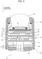
Fig. 3] Fig. 3 is a sectional view in which the electronic device inFig. 1 is rotated around the optical axis by 90° from that in the section inFig. 2 . - [
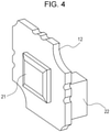
Fig. 4] Fig. 4 is a perspective view illustrating an appearance of a first substrate inFig. 2 andFig. 3 . - [
Fig. 5] Fig. 5 is a perspective view illustrating appearances of a second substrate and a third substrate inFig. 2 andFig. 3 . - [
Fig. 6] Fig. 6 is a perspective view illustrating an appearance of a first metal plate inFig. 2 andFig. 3 . - [
Fig. 7] Fig. 7 is a development plan view of the first metal plate inFig. 6 . - [
Fig. 8] Fig. 8 is a perspective view illustrating an appearance of a second metal plate inFig. 2 andFig. 3 . - [
Fig. 9] Fig. 9 is a development plan view of the second metal plate inFig. 8 . - [
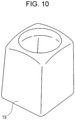
Fig. 10] Fig. 10 is a perspective view illustrating an appearance of a first housing inFig. 2 andFig. 3 . - [
Fig. 11] Fig. 11 is a perspective view illustrating an appearance of a second housing inFig. 2 andFig. 3 . - [
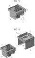
Fig. 12] Fig. 12 illustrates a method of manufacturing the electronic device inFig. 2 andFig. 3 and illustrates a step of assembling a second substrate and a third substrate to a second metal plate. - [
Fig. 13] Fig. 13 illustrates a method of manufacturing the electronic device inFig. 2 andFig. 3 and illustrates another step of assembling a second substrate and a third substrate to a second metal plate. - [
Fig. 14] Fig. 14 illustrates a method of manufacturing the electronic device inFig. 2 andFig. 3 and illustrates yet another step of assembling a second substrate and a third substrate to a second metal plate. - [
Fig. 15] Fig. 15 illustrates a method of manufacturing the electronic device inFig. 2 andFig. 3 and illustrates a step of assembling a second substrate and a third substrate to a first metal plate. - [
Fig. 16] Fig. 16 illustrates a method of manufacturing the electronic device inFig. 2 andFig. 3 and illustrates another step of assembling a second substrate and a third substrate to a first metal plate. - [
Fig. 17] Fig. 17 illustrates a method of manufacturing the electronic device inFig. 2 andFig. 3 and illustrates a step of electrically connecting a first substrate and a second substrate to each other. - [
Fig. 18] Fig. 18 illustrates a method of manufacturing the electronic device inFig. 2 andFig. 3 and illustrates a step of assembling a third substrate to a second housing. Description of Embodiments - Hereinafter, an embodiment of an electronic device to which the present disclosure is applied will be described with reference to the drawings.
- Specifically, an electronic device according to one embodiment of the present disclosure is, for example, an imaging apparatus. As illustrated in
Fig. 1 , anelectronic device 10 applied to the imaging apparatus according to the present embodiment is, for example, mounted on amobile body 11. - The
mobile body 11 may include, for example, vehicles, marine vessels, aircrafts, and the like. Vehicles may include, for example, automobiles, industrial vehicles, railway vehicles, living vehicles, fixed-wing aircrafts that travel on runways, and the like. Automobiles may include, for example, passenger cars, trucks, buses, bicycles, trolley buses, and the like. Industrial vehicles may include, for example, industrial vehicles for agriculture and construction, and the like. Industrial vehicles may include, for example, forklifts, golf carts, and the like. Industrial vehicles for agriculture may include, for example, tractors, cultivators, transplanters, binders, combine harvesters, lawnmowers, and the like. Industrial vehicles for construction may include, for example, bulldozers, scrapers, power shovels, crane trucks, dump trucks, road rollers, and the like. Vehicles may include man-powered vehicles. Classification of vehicles is not limited to the above examples. For example, automobiles may include industrial vehicles that can travel on roads. The same vehicles may be included in a plurality of categories. Marine vessels may include, for example, jet skis, boats, tankers, and the like. Aircrafts may include, for example, fixed-wing aircrafts, rotary-wing aircrafts, and the like. - As illustrated in
Fig. 2 andFig. 3 , theelectronic device 10 includes afirst substrate 12, asecond substrate 13, athird substrate 14, afirst metal plate 15, and asecond metal plate 16. Theelectronic device 10 may further include aheat conductor 17, an imagingoptical system 18, afirst housing 19, and asecond housing 20. - As illustrated in
Fig. 4 , thefirst substrate 12 has a flat shape. Thefirst substrate 12 may have a substantially rectangular shape. As illustrated inFig. 2 andFig. 3 , animaging element 21 as an electronic component is mounted on thefirst substrate 12 on a side opposite to a surface facing a first flat portion, which will be described later. Theimaging element 21 is, for example, a CCD (Charge Coupled Device) image sensor and a CMOS (Complementary Metal Oxide Semiconductor) image sensor. Theimaging element 21 images an optical image formed on a light receiving surface and thereby generates an image signal. Afirst connector 22 for electrical connection to thesecond substrate 13 may be mounted on thefirst substrate 12 at a rear surface of the surface on which theimaging element 21 is mounted. - As illustrated in
Fig. 5 , thesecond substrate 13 has a flat shape. Thesecond substrate 13 may have a substantially rectangular shape. Anelectronic component 23 is mounted on at least one main surface of thesecond substrate 13. Theelectronic component 23 drives theimaging element 21 or processes an image signal generated by theimaging element 21. Asecond connector 24 for electrical connection to thefirst connector 22 may be mounted on one main surface of thesecond substrate 13. - The
third substrate 14 has a flat shape. Thethird substrate 14 may have a substantially rectangular shape. Anelectronic component 23 is mounted on at least one main surface of thethird substrate 14. Theelectronic component 23 drives theimaging element 21 or processes an image signal generated by theimaging element 21. Athird connector 25 for electrical connection to thesecond housing 20 may be mounted on one main surface of thethird substrate 14. - The
third substrate 14 may be electrically connected to thesecond substrate 13 by aflexible substrate 26. Thethird connector 25 may be mounted on a main surface of thethird substrate 14 on the same side as thesecond connector 24 in a state in which the entirety of theflexible substrate 26 is extended in a flat shape. - As illustrated in
Fig. 2 andFig. 3 , in theelectronic device 10, thefirst substrate 12, thesecond substrate 13, and thethird substrate 14 are positioned toward a stacking direction in order with respective main surfaces facing each other. - As illustrated in
Fig. 6 , thefirst metal plate 15 includes a firstflat portion 27 and afirst shield portion 28. Thefirst metal plate 15 may further include athird shield portion 29. - The first
flat portion 27 has a flat shape. The firstflat portion 27 may have a substantially rectangular shape wider than thefirst substrate 12, thesecond substrate 13, and thethird substrate 14. As illustrated inFig. 2 andFig. 3 , in theelectronic device 10, the firstflat portion 27 is interposed between thefirst substrate 12 and thesecond substrate 13. In theelectronic device 10, the firstflat portion 27 may have a main surface substantially parallel to main surfaces of thefirst substrate 12 and thesecond substrate 13. - In the
electronic device 10, the firstflat portion 27 directly or indirectly abuts theelectronic component 23 mounted on thefirst substrate 12 and theelectronic component 23 mounted on thesecond substrate 13. In theelectronic device 10, the firstflat portion 27, for example, abuts theimaging element 21 as an electronic component indirectly via aheat dissipation sheet 30 and thefirst substrate 12. In theelectronic device 10, the firstflat portion 27, for example, abuts theelectronic component 23 mounted on thesecond substrate 13 indirectly via theheat dissipation sheet 30. Theheat dissipation sheet 30 may be made of, for example, a soft material having shape followability, like filler-containing silicone rubber, and having relatively large thermal conductivity. - As illustrated in
Fig. 6 , an opening op may be provided in the firstflat portion 27. The opening op may be larger than thefirst connector 22 viewed in a direction perpendicular to a main surface of thefirst substrate 12. As illustrated inFig. 2 , in theelectronic device 10, thefirst connector 22 may be inserted into the opening op. In theelectronic device 10, thesecond connector 24 may be connected to thefirst connector 22 inserted into the opening op. - As illustrated in
Fig. 6 , thefirst shield portion 28 stands along the whole extent of the outer edge of the firstflat portion 27 on the side of a main surface of the firstflat portion 27 facing thefirst substrate 12. As illustrated inFig. 2 andFig. 3 , in theelectronic device 10, thefirst shield portion 28 covers the entire circumference of the side surface of thefirst substrate 12. - As illustrated in
Fig. 6 , thethird shield portion 29 may stand along two parallel sides of the firstflat portion 27 on a side opposite to the main surface at which thefirst shield portion 28 of the firstflat portion 27 stands. As illustrated inFig. 2 , in theelectronic device 10, thethird shield portion 29 may cover, of side surfaces of thesecond substrate 13 and thethird substrate 14, at least a part exposed from the second shield portion, which will be described later. In theelectronic device 10, thethird shield portion 29 may cover theflexible substrate 26 when viewed in a direction perpendicular to the stacking direction. - The
third shield portion 29 may include afirst leg portion 31 at an end on the side of the stacking direction, in other words, in a direction away from the firstflat portion 27. Thefirst leg portion 31 may be parallel to the firstflat portion 27. Thefirst leg portion 31 may overlap the firstflat portion 27 when viewed in a direction perpendicular to the firstflat portion 27. As illustrated inFig. 2 , inside theelectronic device 10, thethird shield portion 29 may abut theheat conductor 17 at thefirst leg portion 31. - The
first metal plate 15 is a metal plate, in other words, a metal flat plate having a desired shape such as that illustrated inFig. 7 and whose predetermined portions are bent. InFig. 7 , straight lines to be bent on the surface side are indicated by wavy lines, and straight lines to be bent on the rear surface side are indicated by one-dot chain lines. When the bent portions of thefirst metal plate 15 are unbent into a flat shape, all of parts of thefirst metal plate 15 are thus separated from each other without interfering with each other. Thefirst metal plate 15 may be made of, for example, a metal such as copper or the like having large thermal conductivity. - As illustrated in
Fig. 8 , thesecond metal plate 16 includes a secondflat portion 32 and asecond shield portion 33. - The second
flat portion 32 has a flat shape. The secondflat portion 32 may have a substantially rectangular shape wider than thefirst substrate 12, thesecond substrate 13, and thethird substrate 14 and slightly narrower than the firstflat portion 27. As illustrated inFig. 2 andFig. 3 , in theelectronic device 10, the secondflat portion 32 is interposed between thesecond substrate 13 and thethird substrate 14. In theelectronic device 10, the secondflat portion 32 may have a main surface substantially parallel to main surfaces of thesecond substrate 13 and thethird substrate 14. - In the
electronic device 10, the secondflat portion 32 directly or indirectly abuts theelectronic component 23 mounted on thesecond substrate 13 and theelectronic component 23 mounted on thethird substrate 14. In theelectronic device 10, the secondflat portion 32, for example, abuts theelectronic component 23 mounted on thesecond substrate 13 indirectly via theheat dissipation sheet 30. In theelectronic device 10, the secondflat portion 32, for example, abuts theelectronic component 23 mounted on thethird substrate 14 indirectly via theheat dissipation sheet 30. Theheat dissipation sheet 30 may be made of, for example, a soft material having shape followability, like filler-containing silicone rubber, and having relatively large thermal conductivity. - As illustrated in
Fig. 8 , thesecond shield portion 33 includes a first one-side shield portion 34 and a second one-side shield portion 35. The first one-side shield portion 34 stands, on one main surface of the secondflat portion 32, along at least a portion of the outer edge of the secondflat portion 32. The second one-side shield portion 35 stands, on the other main surface of the secondflat portion 32, along at least a portion of the outer edge of the secondflat portion 32. - For example, the first one-
side shield portion 34 stands, on the side of one main surface (the upper side inFig. 8 ), along three sides except for one side of the secondflat portion 32. For example, the second one-side shield portion 35 stands, on the side of the other main surface (the lower side inFig. 8 ), along two mutually facing sides of the three sides along which the first one-side shield portion 34 stands on the side of the one main surface. - As illustrated in
Fig. 2 andFig. 3 , in theelectronic device 10, thesecond shield portion 33 covers at least portions of side surfaces of thesecond substrate 13 and thethird substrate 14. As illustrated inFig. 2 , in theelectronic device 10, thesecond shield portion 33 may cover portions of side surfaces of thesecond substrate 13 and thethird substrate 14 and expose other portions without covering the other portions. - As illustrated in
Fig. 8 , the second one-side shield portion 35 may include asecond leg portion 36 at an end on the side of the stacking direction, in other words, in a direction away from the secondflat portion 32. Thesecond leg portion 36 may be parallel to the secondflat portion 32. Thesecond leg portion 36 may overlap the secondflat portion 32 when viewed in a direction perpendicular to the secondflat portion 32. As illustrated inFig. 3 , inside theelectronic device 10, thesecond shield portion 33 may abut theheat conductor 17 at thesecond leg portion 36. - The
second metal plate 16 is a metal plate, in other words, a metal flat plate having a desired shape such as that illustrated inFig. 9 and whose predetermined portions are bent. InFig. 9 , straight lines to be bent on the surface side are indicated by wavy lines, and straight lines to be bent on the rear surface side are indicated by one-dot chain lines. When the bent portions of thesecond metal plate 16 are unbent into a flat shape, all of parts of thesecond metal plate 16 are thus separated from each other without interfering with each other. Thesecond metal plate 16 may be made of, for example, a metal such as copper or the like having large thermal conductivity. - As illustrated in
Fig. 2 andFig. 3 , thesecond metal plate 16 may be positioned to be separated from thefirst metal plate 15 without being in contact with thefirst metal plate 15 at the all surfaces of thesecond metal plate 16. - As illustrated in
Fig. 2 andFig. 3 , theheat conductor 17 is positioned on the side of the stacking direction from thefirst substrate 12. Theheat conductor 17 may be positioned on the side of the stacking direction from thethird substrate 14. In theelectronic device 10, theheat conductor 17 may abut thefirst metal plate 15 and thesecond metal plate 16. As illustrated inFig. 2 , theheat conductor 17 may abut thefirst metal plate 15 at thefirst leg portion 31. As illustrated inFig. 3 , theheat conductor 17 may abut thesecond metal plate 16 at thesecond leg portion 36. - As illustrated in
Fig. 2 andFig. 3 , theheat conductor 17 may include athird metal plate 37 and aheat dissipation sheet 38. Theheat conductor 17 may abut thefirst metal plate 15 and thesecond metal plate 16 at theheat dissipation sheet 38. Theheat dissipation sheet 38 may abut thethird metal plate 37 at a surface that differs from a surface that abuts thefirst metal plate 15 and thesecond metal plate 16. Theheat dissipation sheet 38 may be made of, for example, a soft material having shape followability, like filler-containing silicone rubber, and having relatively large thermal conductivity. In theelectronic device 10, thethird metal plate 37 extends toward the side of the stacking direction more than the surface that abuts thefirst metal plate 15 and thesecond metal plate 16. Thethird metal plate 37 may be made of, for example, a metal such as copper or the like having large thermal conductivity. - The imaging
optical system 18 is constituted by an optical element such as a lens. The imagingoptical system 18 is designed and formed to have predetermined values of optical characteristics such as angle of field, depth of field, and the like. The imagingoptical system 18 forms an imaged subject image on a light receiving surface of theimaging element 21. - As illustrated in
Fig. 10 , thefirst housing 19 may have a rectangular cylindrical section. As illustrated inFig. 2 andFig. 3 , thefirst housing 19 may house the imagingoptical system 18 with the optical axis of the imagingoptical system 18 substantially coinciding with the axis of thefirst housing 19 and with the imagingoptical system 18 being exposed from one opening. Thefirst housing 19 may house thefirst substrate 12 such that theimaging element 21 is fixed in an orientation determined at a positioned that is determined relative to the imagingoptical system 18. Thefirst housing 19 may house thesecond substrate 13, thethird substrate 14, thefirst metal plate 15, and thesecond metal plate 16 such that the above configuration is satisfied for thefirst substrate 12. - As illustrated in
Fig. 11 , thesecond housing 20 may have a shape including a flat part and a quadrangular prism that extends perpendicular to a main surface of the flat part. Thesecond housing 20 may include thethird metal plate 37 as theheat conductor 17. Thesecond housing 20 may include afourth connector 39 that can be fitted to thethird connector 25. As illustrated inFig. 2 andFig. 3 , thesecond housing 20 may be sealed at the flat part to an opening of thefirst housing 19 at an end on a side opposite to an end on a side that exposes the imagingoptical system 18. - Next, a method of manufacturing the
electronic device 10 will be described below. - As illustrated in
Fig. 12 , thethird substrate 14 is inserted into a space sp1 defined by the secondflat portion 32 and the second one-side shield portion 35 of thesecond metal plate 16. Thethird substrate 14 is inserted into the space sp1 from an outer edge side of the secondflat portion 32 where the first one-side shield portion 34 is not provided. Thethird substrate 14 is inserted such that a main surface opposite to a main surface provided with thethird connector 25 faces the secondflat portion 32. Thethird substrate 14 is inserted into the space sp1 from a side opposite to a side where theflexible substrate 26 is provided. - As illustrated in
Fig. 13 , thethird substrate 14 in the inserted state is stuck to the secondflat portion 32. Theheat dissipation sheet 30 may be used to stick thethird substrate 14 to the secondflat portion 32. As illustrated inFig. 14 , theflexible substrate 26 is folded, and thesecond substrate 13 is stuck to the secondflat portion 32. Theheat dissipation sheet 30 may be used to stick thesecond substrate 13 to the secondflat portion 32. - As illustrated in
Fig. 15 , thesecond metal plate 16 to which thesecond substrate 13 and thethird substrate 14 are stuck is inserted into a space sp2 defined by the firstflat portion 27 and thethird shield portion 29 of thefirst metal plate 15. Thesecond metal plate 16 is inserted such that thesecond substrate 13 faces the firstflat portion 27. - As illustrated in
Fig. 16 , thesecond metal plate 16 is stuck to the firstflat portion 27 via thesecond substrate 13 in a state in which thesecond connector 24 of thesecond substrate 13 is inserted into the opening op of the firstflat portion 27. Theheat dissipation sheet 30 may be used to stick thesecond substrate 13 to the firstflat portion 27. - As illustrated in
Fig. 17 , thesecond substrate 13 assembled to thefirst metal plate 15 and thesecond metal plate 16 is connected to thefirst substrate 12 by thesecond connector 24 being fitted to thefirst connector 22. Before the connection, thefirst substrate 12 is fixed to alens barrel 40 housing the imagingoptical system 18 while aheat conduction member 41 such as a metal plate being interposed therebetween. For example, bonding with an adhesive, fastening with a screw, and the like are employed for fixation of thefirst substrate 12 to thelens barrel 40. - As illustrated in
Fig. 18 , thethird substrate 14 is connected to thesecond housing 20 by thethird connector 25 being fitted to thefourth connector 39 in a state in which thesecond substrate 13 is connected to thefirst substrate 12. Thereafter, thefirst housing 19 is placed over the imagingoptical system 18, thefirst substrate 12, thesecond substrate 13, thethird substrate 14, thefirst metal plate 15, and thesecond metal plate 16. In the state in which thefirst housing 19 is placed, thefirst housing 19 is fixed to thesecond housing 20, and theelectronic device 10 is thereby manufactured. For example, welding, bonding with an adhesive, fastening with a screw, and the like are employed for fixation of thefirst housing 19 and thesecond housing 20. - The
electronic device 10 in the present embodiment with the above configuration includes the firstflat portion 27 that is interposed between thefirst substrate 12 and thesecond substrate 13 and that indirectly abuts theimaging element 21 mounted on thefirst substrate 12 and theelectronic component 23 mounted on thesecond substrate 13. In theelectronic device 10 with such a configuration, theimaging element 21 mounted on thefirst substrate 12 and theelectronic component 23 mounted on thesecond substrate 13, which are heat sources, are close to the firstflat portion 27, which generally has thermal conductivity higher than that of theheat dissipation sheet 30. Thus, heat dissipation properties are improved compared with a configuration in which only theheat dissipation sheet 30 is interposed. In addition, theelectronic device 10 includes the secondflat portion 32 that is interposed between thesecond substrate 13 and thethird substrate 14 and that indirectly abuts theelectronic component 23 mounted on thesecond substrate 13 and theelectronic component 23 mounted on thethird substrate 14. In theelectronic device 10 with such a configuration, theelectronic component 23 mounted on thesecond substrate 13 and theelectronic component 23 mounted on thethird substrate 14, which are heat sources, are close to the secondflat portion 32, which generally has heat dissipation properties higher than that of theheat dissipation sheet 30. Thus, heat dissipation properties are improved compared with a configuration in which only theheat dissipation sheet 30 is interposed. - The
electronic device 10 according to the present embodiment further includes thefirst shield portion 28 that covers the entire circumference of the side surface of thefirst substrate 12. With such a configuration, theelectronic device 10 can have shielding properties with respect to radiation noise of thefirst substrate 12 or theelectronic component 23 mounted on thefirst substrate 12. In addition, theelectronic device 10 includes thesecond shield portion 33 that covers at least portions of the side surfaces of thesecond substrate 13 and thethird substrate 14. With such a configuration, theelectronic device 10 can have shielding properties with respect to radiation noise of theelectronic component 23 mounted on thesecond substrate 13 and theelectronic component 23 mounted on thethird substrate 14. - In the
electronic device 10 according to the present embodiment, thefirst metal plate 15 includes the firstflat portion 27 and thefirst shield portion 28. In addition, in theelectronic device 10, thesecond metal plate 16 includes the secondflat portion 32 and thesecond shield portion 33. In theelectronic device 10 with such a configuration, the firstflat portion 27 and thefirst shield portion 28 having the above configuration and the secondflat portion 32 and thesecond shield portion 33 having the above configuration can be manufactured in a simple configuration without being subjected to steps of welding and the like. - Therefore, as described above, the
electronic device 10 according to the present embodiment can further improve heat dissipation properties with a simple configuration while having shielding properties with respect to radiation noise. - In the
electronic device 10 according to the present embodiment, thefirst metal plate 15 and thesecond metal plate 16 are positioned to be separated from each other. With such a configuration, theelectronic device 10 can reduce heat conduction between thefirst metal plate 15 and thesecond metal plate 16 compared with a configuration in which thefirst metal plate 15 and thesecond metal plate 16 abut each other. Thus, in a configuration in which one of thefirst metal plate 15 and thesecond metal plate 16 is close to a component that is to be greatly affected by a high temperature, theelectronic device 10 can reduce heat conduction from the other one to the one even when the temperature of the other one is increased. - In the
electronic device 10 according to the present embodiment, thesecond shield portion 33 covers portions of the side surfaces of thesecond substrate 13 and thethird substrate 14, and thethird shield portion 29 of thefirst metal plate 15 covers at least a part exposed from thesecond shield portion 33. With such a configuration, theelectronic device 10 can have shielding properties with respect to radiation noise of theelectronic component 23 mounted on thesecond substrate 13 and theelectronic component 23 mounted on thethird substrate 14 while enabling thesecond substrate 13 and thethird substrate 14 to be easily stuck to thesecond metal plate 16, even in a configuration in which thesecond substrate 13 and thethird substrate 14 are connected to each other by a wire or the like, such as theflexible substrate 26, extending from the side surfaces of thesecond substrate 13 and thethird substrate 14. - In the
electronic device 10 according to the present embodiment, theflexible substrate 26 that connects thesecond substrate 13 and thethird substrate 14 to each other is covered by thethird shield portion 29. With such a configuration, theelectronic device 10 can suppress degradation of shielding properties with respect to radiation noise of theelectronic component 23 mounted on thesecond substrate 13 and theelectronic component 23 mounted on thethird substrate 14 while using theflexible substrate 26 that contributes to easy manufacture and a reduction in manufacturing costs. - The
electronic device 10 according to the present embodiment includes theheat conductor 17 that is positioned on the side of the stacking direction from thefirst substrate 12 and that abuts thefirst metal plate 15 and thesecond metal plate 16. With such a configuration, theelectronic device 10 can conduct heat generated at theelectronic component 23 mounted on thefirst substrate 12, theelectronic component 23 mounted on thesecond substrate 13, and theelectronic component 23 mounted on thethird substrate 14 toward the stacking direction. Thus, even in a configuration in which a component that is to be greatly affected by a high temperature, as with the imagingoptical system 18 made of a resin, is positioned in a direction opposite the stacking direction, theelectronic device 10 can suppress a heat increase of the component. - In the
electronic device 10 according to the present embodiment, thethird shield portion 29 and thesecond shield portion 33 abut theheat conductor 17 at thefirst leg portion 31 and thesecond leg portion 36, respectively. With such a configuration, theelectronic device 10 according to the present embodiment can increase an area of contact between each of thefirst metal plate 15 and thesecond metal plate 16, and theheat conductor 17. Thus, theelectronic device 10 can improve conduction of the heat generated at theelectronic component 23 mounted on thefirst substrate 12, theelectronic component 23 mounted on thesecond substrate 13, and theelectronic component 23 mounted on thethird substrate 14 to theheat conductor 17. - In the
electronic device 10 according to the present embodiment, thefirst substrate 12 and thesecond substrate 13 are electrically connected to each other via thefirst connector 22 inserted into the opening op provided in the firstflat portion 27, and thesecond connector 24. With such a configuration, theelectronic device 10 can allow formation of thefirst shield portion 28 and thethird shield portion 29 that cover the entirety of the side surface of at least one of thefirst substrate 12 and thesecond substrate 13. Therefore, theelectronic device 10 can cover the entire circumference of the side surface of at least one of thefirst substrate 12 and thesecond substrate 13 by using the singlefirst metal plate 15 without using a plurality of metal plates. - Although the present invention has been described on the basis of the drawings and the embodiment, it should be noted that it is easy for a person skilled in the art to perform various changes and corrections on the basis of the present disclosure. Accordingly, it should be noted that these changes and corrections are included in the scope of the present invention.
- For example, in the present embodiment, the
second substrate 13 and thethird substrate 14 are configured to be connected to each other via theflexible substrate 26. However, an opening may be provided in the secondflat portion 32, and thesecond substrate 13 and thethird substrate 14 may be connected to each other by a connector through the opening. In such a configuration, thesecond shield portion 33 may cover the entire circumference of the side surfaces of thesecond substrate 13 and thethird substrate 14. Since the side surfaces of thesecond substrate 13 and thethird substrate 14 are covered at the entire circumference thereof, thethird shield portion 29 may not cover portions of the side surfaces of thesecond substrate 13 and thethird substrate 14. Thus, an electronic device including a plurality of substrates positioned to be side by side toward a stacking direction, a flat portion interposed between, of the plurality of substrates, mutually adjacent two substrates, and a metal plate including a shield portion that covers the entire circumference of side surfaces of the two substrates can further improve heat dissipation properties with a simple configuration while having shielding properties with respect to radiation noise, as described above. -
- 10
- electronic device
- 11
- mobile body
- 12
- first substrate
- 13
- second substrate
- 14
- third substrate
- 15
- first metal plate
- 16
- second metal plate
- 17
- heat conductor
- 18
- imaging optical system
- 19
- first housing
- 20
- second housing
- 21
- imaging element
- 22
- first connector
- 23
- electronic component
- 24
- second connector
- 25
- third connector
- 26
- flexible substrate
- 27
- first flat portion
- 28
- first shield portion
- 29
- third shield portion
- 30
- heat dissipation sheet
- 31
- first leg portion
- 32
- second flat portion
- 33
- second shield portion
- 34
- first one-side shield portion
- 35
- second one-side shield portion
- 36
- second leg portion
- 37
- third metal plate
- 38
- heat dissipation sheet
- 39
- fourth connector
- 40
- lens barrel
- 41
- heat conduction member
- op
- opening
- sp1
- space defined by second flat portion and second one-side shield portion
- sp2
- space defined by first flat portion and third shield portion
Claims (9)
- An electronic device comprising:a first substrate, a second substrate, and a third substrate on each of which an electronic component is mounted, the first substrate, the second substrate, and the third substrate being positioned in order toward a stacking direction with respective main surfaces facing each other;a first metal plate including a first flat portion that is interposed between the first substrate and the second substrate and that directly or indirectly abuts the electronic component mounted on the first substrate and the electronic component mounted on the second substrate, and a first shield portion that covers an entire circumference of a side surface of the first substrate; anda second metal plate including a second flat portion that is interposed between the second substrate and the third substrate and that directly or indirectly abuts the electronic component mounted on the second substrate and the electronic component mounted on the third substrate, and a second shield portion that covers at least portions of side surfaces of the second substrate and the third substrate.
- The electronic device according to claim 1,
wherein the first metal plate and the second metal plate are positioned to be separated from each other. - The electronic device according to claim 1 or claim 2, wherein the second shield portion covers portions of the side surfaces of the second substrate and the third substrate, and
the first metal plate further includes a third shield portion that covers, of the side surfaces of the second substrate and the third substrate, at least a part exposed from the second shield portion. - The electronic device according to claim 3,wherein the second substrate and the third substrate are connected to each other by a flexible substrate, andthe flexible substrate is covered by the third shield portion when viewed in a direction perpendicular to the stacking direction.
- The electronic device according to any one of claims 1 to 4,
wherein the first substrate includes an imaging element as the electronic component on a side opposite to a surface facing the first flat portion. - The electronic device according to claim 1, further comprising:a heat conductor positioned on a side of the stacking direction from the first substrate,wherein the first metal plate and the second metal plate abut the heat conductor.
- An electronic device comprising:a plurality of substrates on each of which an electronic component is mounted, the plurality of substrates being positioned to be side by side toward a stacking direction with respective main surfaces facing each other; anda metal plate including a flat portion that is interposed between, of the plurality of substrates, mutually adjacent two substrates and that directly or indirectly abuts the electronic component mounted on one of the two substrates and the electronic component mounted on another of the two substrates, and a shield portion that covers an entire circumference of side surfaces of the two substrates.
- An imaging apparatus comprising:a first substrate, a second substrate, and a third substrate on each of which an electronic component is mounted, the first substrate, the second substrate, and the third substrate being positioned in order toward a stacking direction with respective main surfaces facing each other;a first metal plate including a first flat portion that is interposed between the first substrate and the second substrate and that directly or indirectly abuts the electronic component mounted on the first substrate and the electronic component mounted on the second substrate, and a first shield portion that covers an entire circumference of a side surface of the first substrate; anda second metal plate including a second flat portion that is interposed between the second substrate and the third substrate and that directly or indirectly abuts the electronic component mounted on the second substrate and the electronic component mounted on the third substrate, and a second shield portion that covers at least portions of side surfaces of the second substrate and the third substrate.
- A mobile body comprising the imaging apparatus according to claim 8 mounted thereon.
Priority Applications (1)
| Application Number | Priority Date | Filing Date | Title |
|---|---|---|---|
| EP25150033.6A EP4510602A3 (en) | 2019-03-20 | 2020-03-12 | Electronic device, imaging apparatus, and mobile body |
Applications Claiming Priority (2)
| Application Number | Priority Date | Filing Date | Title |
|---|---|---|---|
| JP2019053726A JP7074707B2 (en) | 2019-03-20 | 2019-03-20 | Electronic devices, imaging devices, and moving objects |
| PCT/JP2020/010835 WO2020189505A1 (en) | 2019-03-20 | 2020-03-12 | Electronic instrument, image capture device, and mobile body |
Related Child Applications (2)
| Application Number | Title | Priority Date | Filing Date |
|---|---|---|---|
| EP25150033.6A Division-Into EP4510602A3 (en) | 2019-03-20 | 2020-03-12 | Electronic device, imaging apparatus, and mobile body |
| EP25150033.6A Division EP4510602A3 (en) | 2019-03-20 | 2020-03-12 | Electronic device, imaging apparatus, and mobile body |
Publications (3)
| Publication Number | Publication Date |
|---|---|
| EP3944606A1 true EP3944606A1 (en) | 2022-01-26 |
| EP3944606A4 EP3944606A4 (en) | 2022-12-28 |
| EP3944606B1 EP3944606B1 (en) | 2025-02-19 |
Family
ID=72519093
Family Applications (2)
| Application Number | Title | Priority Date | Filing Date |
|---|---|---|---|
| EP20774708.0A Active EP3944606B1 (en) | 2019-03-20 | 2020-03-12 | Electronic instrument, image capture device, and mobile body |
| EP25150033.6A Pending EP4510602A3 (en) | 2019-03-20 | 2020-03-12 | Electronic device, imaging apparatus, and mobile body |
Family Applications After (1)
| Application Number | Title | Priority Date | Filing Date |
|---|---|---|---|
| EP25150033.6A Pending EP4510602A3 (en) | 2019-03-20 | 2020-03-12 | Electronic device, imaging apparatus, and mobile body |
Country Status (5)
| Country | Link |
|---|---|
| US (2) | US11863852B2 (en) |
| EP (2) | EP3944606B1 (en) |
| JP (1) | JP7074707B2 (en) |
| CN (1) | CN113632446B (en) |
| WO (1) | WO2020189505A1 (en) |
Cited By (1)
| Publication number | Priority date | Publication date | Assignee | Title |
|---|---|---|---|---|
| US11877430B2 (en) | 2021-05-21 | 2024-01-16 | Panasonic Intellectual Property Management Co., Ltd. | Imaging device |
Family Cites Families (12)
| Publication number | Priority date | Publication date | Assignee | Title |
|---|---|---|---|---|
| JP5565117B2 (en) | 2010-06-07 | 2014-08-06 | 株式会社リコー | Imaging device |
| EP2696575B1 (en) | 2011-04-05 | 2018-10-10 | Panasonic Intellectual Property Management Co., Ltd. | Solid-state image pickup device, and method for manufacturing solid-state image pickup device |
| JP6000337B2 (en) | 2012-04-04 | 2016-09-28 | 富士機械製造株式会社 | Imaging device |
| TWI479086B (en) * | 2012-10-23 | 2015-04-01 | Sunonwealth Electr Mach Ind Co | Cooling fan |
| JP5983317B2 (en) * | 2012-11-01 | 2016-08-31 | 住友電気工業株式会社 | Electronic device with cable and method of assembling the same |
| EP3163864B1 (en) * | 2014-06-26 | 2019-11-06 | Kyocera Corporation | Image-capturing device and vehicle |
| KR102248086B1 (en) * | 2014-11-14 | 2021-05-04 | 엘지이노텍 주식회사 | Camera module using for automobile |
| WO2016103490A1 (en) * | 2014-12-26 | 2016-06-30 | 三菱電機株式会社 | Electronic apparatus and electronic apparatus system |
| JP2017044795A (en) * | 2015-08-25 | 2017-03-02 | オリンパス株式会社 | Imaging device |
| JP6732438B2 (en) * | 2015-11-27 | 2020-07-29 | 京セラ株式会社 | Imaging device |
| CN105845440B (en) * | 2016-04-11 | 2017-09-01 | 珠海英搏尔电气股份有限公司 | AC motor control, capacitor array and preparation method thereof |
| EP4525470A3 (en) * | 2016-04-14 | 2025-06-11 | Lg Innotek Co. Ltd | Device for fixing camera module circuit board, and camera module |
-
2019
- 2019-03-20 JP JP2019053726A patent/JP7074707B2/en active Active
-
2020
- 2020-03-12 EP EP20774708.0A patent/EP3944606B1/en active Active
- 2020-03-12 CN CN202080022590.1A patent/CN113632446B/en active Active
- 2020-03-12 US US17/438,689 patent/US11863852B2/en active Active
- 2020-03-12 WO PCT/JP2020/010835 patent/WO2020189505A1/en not_active Ceased
- 2020-03-12 EP EP25150033.6A patent/EP4510602A3/en active Pending
-
2023
- 2023-11-17 US US18/512,442 patent/US12219230B2/en active Active
Cited By (2)
| Publication number | Priority date | Publication date | Assignee | Title |
|---|---|---|---|---|
| US11877430B2 (en) | 2021-05-21 | 2024-01-16 | Panasonic Intellectual Property Management Co., Ltd. | Imaging device |
| US12250799B2 (en) | 2021-05-21 | 2025-03-11 | Panasonic Automotive Systems Co., Ltd. | Imaging device |
Also Published As
| Publication number | Publication date |
|---|---|
| EP3944606A4 (en) | 2022-12-28 |
| JP2020155985A (en) | 2020-09-24 |
| US11863852B2 (en) | 2024-01-02 |
| WO2020189505A1 (en) | 2020-09-24 |
| EP3944606B1 (en) | 2025-02-19 |
| US20220150388A1 (en) | 2022-05-12 |
| US12219230B2 (en) | 2025-02-04 |
| EP4510602A2 (en) | 2025-02-19 |
| CN113632446B (en) | 2023-08-01 |
| US20240089572A1 (en) | 2024-03-14 |
| EP4510602A3 (en) | 2025-05-07 |
| JP7074707B2 (en) | 2022-05-24 |
| CN113632446A (en) | 2021-11-09 |
Similar Documents
| Publication | Publication Date | Title |
|---|---|---|
| US12568291B2 (en) | Electronic device, imaging apparatus, and mobile body | |
| EP3961300B1 (en) | Electronic instrument, imaging device, and mobile body | |
| US12219230B2 (en) | Electronic device, imaging apparatus, and mobile body | |
| CN116866697A (en) | Electronic equipment | |
| CN114450931A (en) | Imaging device and moving object | |
| JP7069064B2 (en) | Imaging devices, in-vehicle cameras and vehicles | |
| CN104954641A (en) | Camera module | |
| JP7224514B2 (en) | Electronic devices, imaging devices, and mobile objects | |
| CN108702436A (en) | Electronic part-mounting component, photographic device and vehicle-mounted photographic device | |
| WO2020003838A1 (en) | Bonded structure, imaging device, and moving body |
Legal Events
| Date | Code | Title | Description |
|---|---|---|---|
| STAA | Information on the status of an ep patent application or granted ep patent |
Free format text: STATUS: THE INTERNATIONAL PUBLICATION HAS BEEN MADE |
|
| PUAI | Public reference made under article 153(3) epc to a published international application that has entered the european phase |
Free format text: ORIGINAL CODE: 0009012 |
|
| STAA | Information on the status of an ep patent application or granted ep patent |
Free format text: STATUS: REQUEST FOR EXAMINATION WAS MADE |
|
| 17P | Request for examination filed |
Effective date: 20210913 |
|
| AK | Designated contracting states |
Kind code of ref document: A1 Designated state(s): AL AT BE BG CH CY CZ DE DK EE ES FI FR GB GR HR HU IE IS IT LI LT LU LV MC MK MT NL NO PL PT RO RS SE SI SK SM TR |
|
| DAV | Request for validation of the european patent (deleted) | ||
| DAX | Request for extension of the european patent (deleted) | ||
| A4 | Supplementary search report drawn up and despatched |
Effective date: 20221128 |
|
| RIC1 | Information provided on ipc code assigned before grant |
Ipc: H05K 9/00 20060101ALI20221122BHEP Ipc: H05K 7/20 20060101ALI20221122BHEP Ipc: G03B 17/55 20210101ALI20221122BHEP Ipc: G03B 17/02 20210101ALI20221122BHEP Ipc: G03B 15/00 20210101ALI20221122BHEP Ipc: H04N 5/225 20060101AFI20221122BHEP |
|
| P01 | Opt-out of the competence of the unified patent court (upc) registered |
Effective date: 20230505 |
|
| REG | Reference to a national code |
Ref country code: DE Ref legal event code: R079 Free format text: PREVIOUS MAIN CLASS: H04N0005225000 Ipc: H04N0023520000 Ref country code: DE Ref legal event code: R079 Ref document number: 602020046354 Country of ref document: DE Free format text: PREVIOUS MAIN CLASS: H04N0005225000 Ipc: H04N0023520000 |
|
| RIC1 | Information provided on ipc code assigned before grant |
Ipc: H04N 23/57 20230101ALI20240729BHEP Ipc: H04N 23/54 20230101ALI20240729BHEP Ipc: H05K 9/00 20060101ALI20240729BHEP Ipc: H05K 7/20 20060101ALI20240729BHEP Ipc: G03B 17/55 20210101ALI20240729BHEP Ipc: G03B 17/02 20210101ALI20240729BHEP Ipc: G03B 15/00 20210101ALI20240729BHEP Ipc: H04N 23/52 20230101AFI20240729BHEP |
|
| GRAP | Despatch of communication of intention to grant a patent |
Free format text: ORIGINAL CODE: EPIDOSNIGR1 |
|
| STAA | Information on the status of an ep patent application or granted ep patent |
Free format text: STATUS: GRANT OF PATENT IS INTENDED |
|
| INTG | Intention to grant announced |
Effective date: 20240916 |
|
| GRAS | Grant fee paid |
Free format text: ORIGINAL CODE: EPIDOSNIGR3 |
|
| GRAA | (expected) grant |
Free format text: ORIGINAL CODE: 0009210 |
|
| STAA | Information on the status of an ep patent application or granted ep patent |
Free format text: STATUS: THE PATENT HAS BEEN GRANTED |
|
| AK | Designated contracting states |
Kind code of ref document: B1 Designated state(s): AL AT BE BG CH CY CZ DE DK EE ES FI FR GB GR HR HU IE IS IT LI LT LU LV MC MK MT NL NO PL PT RO RS SE SI SK SM TR |
|
| REG | Reference to a national code |
Ref country code: GB Ref legal event code: FG4D |
|
| REG | Reference to a national code |
Ref country code: CH Ref legal event code: EP |
|
| REG | Reference to a national code |
Ref country code: IE Ref legal event code: FG4D |
|
| REG | Reference to a national code |
Ref country code: DE Ref legal event code: R096 Ref document number: 602020046354 Country of ref document: DE |
|
| REG | Reference to a national code |
Ref country code: NL Ref legal event code: MP Effective date: 20250219 |
|
| PG25 | Lapsed in a contracting state [announced via postgrant information from national office to epo] |
Ref country code: RS Free format text: LAPSE BECAUSE OF FAILURE TO SUBMIT A TRANSLATION OF THE DESCRIPTION OR TO PAY THE FEE WITHIN THE PRESCRIBED TIME-LIMIT Effective date: 20250519 |
|
| PG25 | Lapsed in a contracting state [announced via postgrant information from national office to epo] |
Ref country code: FI Free format text: LAPSE BECAUSE OF FAILURE TO SUBMIT A TRANSLATION OF THE DESCRIPTION OR TO PAY THE FEE WITHIN THE PRESCRIBED TIME-LIMIT Effective date: 20250219 |
|
| PG25 | Lapsed in a contracting state [announced via postgrant information from national office to epo] |
Ref country code: PL Free format text: LAPSE BECAUSE OF FAILURE TO SUBMIT A TRANSLATION OF THE DESCRIPTION OR TO PAY THE FEE WITHIN THE PRESCRIBED TIME-LIMIT Effective date: 20250219 |
|
| PG25 | Lapsed in a contracting state [announced via postgrant information from national office to epo] |
Ref country code: ES Free format text: LAPSE BECAUSE OF FAILURE TO SUBMIT A TRANSLATION OF THE DESCRIPTION OR TO PAY THE FEE WITHIN THE PRESCRIBED TIME-LIMIT Effective date: 20250219 |
|
| REG | Reference to a national code |
Ref country code: LT Ref legal event code: MG9D |
|
| PG25 | Lapsed in a contracting state [announced via postgrant information from national office to epo] |
Ref country code: NO Free format text: LAPSE BECAUSE OF FAILURE TO SUBMIT A TRANSLATION OF THE DESCRIPTION OR TO PAY THE FEE WITHIN THE PRESCRIBED TIME-LIMIT Effective date: 20250519 Ref country code: IS Free format text: LAPSE BECAUSE OF FAILURE TO SUBMIT A TRANSLATION OF THE DESCRIPTION OR TO PAY THE FEE WITHIN THE PRESCRIBED TIME-LIMIT Effective date: 20250619 |
|
| PG25 | Lapsed in a contracting state [announced via postgrant information from national office to epo] |
Ref country code: NL Free format text: LAPSE BECAUSE OF FAILURE TO SUBMIT A TRANSLATION OF THE DESCRIPTION OR TO PAY THE FEE WITHIN THE PRESCRIBED TIME-LIMIT Effective date: 20250219 |
|
| PG25 | Lapsed in a contracting state [announced via postgrant information from national office to epo] |
Ref country code: HR Free format text: LAPSE BECAUSE OF FAILURE TO SUBMIT A TRANSLATION OF THE DESCRIPTION OR TO PAY THE FEE WITHIN THE PRESCRIBED TIME-LIMIT Effective date: 20250219 |
|
| PG25 | Lapsed in a contracting state [announced via postgrant information from national office to epo] |
Ref country code: PT Free format text: LAPSE BECAUSE OF FAILURE TO SUBMIT A TRANSLATION OF THE DESCRIPTION OR TO PAY THE FEE WITHIN THE PRESCRIBED TIME-LIMIT Effective date: 20250620 Ref country code: LV Free format text: LAPSE BECAUSE OF FAILURE TO SUBMIT A TRANSLATION OF THE DESCRIPTION OR TO PAY THE FEE WITHIN THE PRESCRIBED TIME-LIMIT Effective date: 20250219 |
|
| PG25 | Lapsed in a contracting state [announced via postgrant information from national office to epo] |
Ref country code: GR Free format text: LAPSE BECAUSE OF FAILURE TO SUBMIT A TRANSLATION OF THE DESCRIPTION OR TO PAY THE FEE WITHIN THE PRESCRIBED TIME-LIMIT Effective date: 20250520 Ref country code: BG Free format text: LAPSE BECAUSE OF FAILURE TO SUBMIT A TRANSLATION OF THE DESCRIPTION OR TO PAY THE FEE WITHIN THE PRESCRIBED TIME-LIMIT Effective date: 20250219 |
|
| REG | Reference to a national code |
Ref country code: AT Ref legal event code: MK05 Ref document number: 1769505 Country of ref document: AT Kind code of ref document: T Effective date: 20250219 |
|
| PG25 | Lapsed in a contracting state [announced via postgrant information from national office to epo] |
Ref country code: SE Free format text: LAPSE BECAUSE OF FAILURE TO SUBMIT A TRANSLATION OF THE DESCRIPTION OR TO PAY THE FEE WITHIN THE PRESCRIBED TIME-LIMIT Effective date: 20250219 |
|
| PG25 | Lapsed in a contracting state [announced via postgrant information from national office to epo] |
Ref country code: SM Free format text: LAPSE BECAUSE OF FAILURE TO SUBMIT A TRANSLATION OF THE DESCRIPTION OR TO PAY THE FEE WITHIN THE PRESCRIBED TIME-LIMIT Effective date: 20250219 |
|
| PG25 | Lapsed in a contracting state [announced via postgrant information from national office to epo] |
Ref country code: DK Free format text: LAPSE BECAUSE OF FAILURE TO SUBMIT A TRANSLATION OF THE DESCRIPTION OR TO PAY THE FEE WITHIN THE PRESCRIBED TIME-LIMIT Effective date: 20250219 |
|
| PG25 | Lapsed in a contracting state [announced via postgrant information from national office to epo] |
Ref country code: IT Free format text: LAPSE BECAUSE OF FAILURE TO SUBMIT A TRANSLATION OF THE DESCRIPTION OR TO PAY THE FEE WITHIN THE PRESCRIBED TIME-LIMIT Effective date: 20250219 |
|
| PG25 | Lapsed in a contracting state [announced via postgrant information from national office to epo] |
Ref country code: AT Free format text: LAPSE BECAUSE OF FAILURE TO SUBMIT A TRANSLATION OF THE DESCRIPTION OR TO PAY THE FEE WITHIN THE PRESCRIBED TIME-LIMIT Effective date: 20250219 |
|
| PG25 | Lapsed in a contracting state [announced via postgrant information from national office to epo] |
Ref country code: EE Free format text: LAPSE BECAUSE OF FAILURE TO SUBMIT A TRANSLATION OF THE DESCRIPTION OR TO PAY THE FEE WITHIN THE PRESCRIBED TIME-LIMIT Effective date: 20250219 Ref country code: CZ Free format text: LAPSE BECAUSE OF FAILURE TO SUBMIT A TRANSLATION OF THE DESCRIPTION OR TO PAY THE FEE WITHIN THE PRESCRIBED TIME-LIMIT Effective date: 20250219 |
|
| PG25 | Lapsed in a contracting state [announced via postgrant information from national office to epo] |
Ref country code: RO Free format text: LAPSE BECAUSE OF FAILURE TO SUBMIT A TRANSLATION OF THE DESCRIPTION OR TO PAY THE FEE WITHIN THE PRESCRIBED TIME-LIMIT Effective date: 20250219 |
|
| REG | Reference to a national code |
Ref country code: CH Ref legal event code: H13 Free format text: ST27 STATUS EVENT CODE: U-0-0-H10-H13 (AS PROVIDED BY THE NATIONAL OFFICE) Effective date: 20251023 |
|
| PG25 | Lapsed in a contracting state [announced via postgrant information from national office to epo] |
Ref country code: SK Free format text: LAPSE BECAUSE OF FAILURE TO SUBMIT A TRANSLATION OF THE DESCRIPTION OR TO PAY THE FEE WITHIN THE PRESCRIBED TIME-LIMIT Effective date: 20250219 |
|
| PG25 | Lapsed in a contracting state [announced via postgrant information from national office to epo] |
Ref country code: LU Free format text: LAPSE BECAUSE OF NON-PAYMENT OF DUE FEES Effective date: 20250312 |
|
| REG | Reference to a national code |
Ref country code: DE Ref legal event code: R097 Ref document number: 602020046354 Country of ref document: DE |
|
| REG | Reference to a national code |
Ref country code: BE Ref legal event code: MM Effective date: 20250331 |
|
| PG25 | Lapsed in a contracting state [announced via postgrant information from national office to epo] |
Ref country code: MC Free format text: LAPSE BECAUSE OF FAILURE TO SUBMIT A TRANSLATION OF THE DESCRIPTION OR TO PAY THE FEE WITHIN THE PRESCRIBED TIME-LIMIT Effective date: 20250219 |
|
| PLBE | No opposition filed within time limit |
Free format text: ORIGINAL CODE: 0009261 |
|
| STAA | Information on the status of an ep patent application or granted ep patent |
Free format text: STATUS: NO OPPOSITION FILED WITHIN TIME LIMIT |
|
| PG25 | Lapsed in a contracting state [announced via postgrant information from national office to epo] |
Ref country code: BE Free format text: LAPSE BECAUSE OF NON-PAYMENT OF DUE FEES Effective date: 20250331 |
|
| PG25 | Lapsed in a contracting state [announced via postgrant information from national office to epo] |
Ref country code: CH Free format text: LAPSE BECAUSE OF NON-PAYMENT OF DUE FEES Effective date: 20250331 |
|
| PG25 | Lapsed in a contracting state [announced via postgrant information from national office to epo] |
Ref country code: IE Free format text: LAPSE BECAUSE OF NON-PAYMENT OF DUE FEES Effective date: 20250312 |
|
| 26N | No opposition filed |
Effective date: 20251120 |
|
| PGFP | Annual fee paid to national office [announced via postgrant information from national office to epo] |
Ref country code: GB Payment date: 20260202 Year of fee payment: 7 |
|
| PGFP | Annual fee paid to national office [announced via postgrant information from national office to epo] |
Ref country code: DE Payment date: 20260128 Year of fee payment: 7 |
|
| PGFP | Annual fee paid to national office [announced via postgrant information from national office to epo] |
Ref country code: FR Payment date: 20260209 Year of fee payment: 7 |