EP3944494A1 - Driving circuit with energy recycle capability - Google Patents
Driving circuit with energy recycle capability Download PDFInfo
- Publication number
- EP3944494A1 EP3944494A1 EP21184467.5A EP21184467A EP3944494A1 EP 3944494 A1 EP3944494 A1 EP 3944494A1 EP 21184467 A EP21184467 A EP 21184467A EP 3944494 A1 EP3944494 A1 EP 3944494A1
- Authority
- EP
- European Patent Office
- Prior art keywords
- switch
- terminal
- voltage
- capacitive load
- phase
- Prior art date
- Legal status (The legal status is an assumption and is not a legal conclusion. Google has not performed a legal analysis and makes no representation as to the accuracy of the status listed.)
- Withdrawn
Links
Images


Classifications
-
- H—ELECTRICITY
- H02—GENERATION; CONVERSION OR DISTRIBUTION OF ELECTRIC POWER
- H02M—APPARATUS FOR CONVERSION BETWEEN AC AND AC, BETWEEN AC AND DC, OR BETWEEN DC AND DC, AND FOR USE WITH MAINS OR SIMILAR POWER SUPPLY SYSTEMS; CONVERSION OF DC OR AC INPUT POWER INTO SURGE OUTPUT POWER; CONTROL OR REGULATION THEREOF
- H02M3/00—Conversion of DC power input into DC power output
- H02M3/02—Conversion of DC power input into DC power output without intermediate conversion into AC
- H02M3/04—Conversion of DC power input into DC power output without intermediate conversion into AC by static converters
- H02M3/10—Conversion of DC power input into DC power output without intermediate conversion into AC by static converters using discharge tubes with control electrode or semiconductor devices with control electrode
- H02M3/145—Conversion of DC power input into DC power output without intermediate conversion into AC by static converters using discharge tubes with control electrode or semiconductor devices with control electrode using devices of a triode or transistor type requiring continuous application of a control signal
- H02M3/155—Conversion of DC power input into DC power output without intermediate conversion into AC by static converters using discharge tubes with control electrode or semiconductor devices with control electrode using devices of a triode or transistor type requiring continuous application of a control signal using semiconductor devices only
- H02M3/156—Conversion of DC power input into DC power output without intermediate conversion into AC by static converters using discharge tubes with control electrode or semiconductor devices with control electrode using devices of a triode or transistor type requiring continuous application of a control signal using semiconductor devices only with automatic control of output voltage or current, e.g. switching regulators
- H02M3/158—Conversion of DC power input into DC power output without intermediate conversion into AC by static converters using discharge tubes with control electrode or semiconductor devices with control electrode using devices of a triode or transistor type requiring continuous application of a control signal using semiconductor devices only with automatic control of output voltage or current, e.g. switching regulators including plural semiconductor devices as final control devices for a single load
- H02M3/1582—Buck-boost converters
-
- H—ELECTRICITY
- H04—ELECTRIC COMMUNICATION TECHNIQUE
- H04R—LOUDSPEAKERS, MICROPHONES, GRAMOPHONE PICK-UPS OR LIKE ACOUSTIC ELECTROMECHANICAL TRANSDUCERS; ELECTRIC HEARING AIDS; PUBLIC ADDRESS SYSTEMS
- H04R3/00—Circuits for transducers
-
- H—ELECTRICITY
- H03—ELECTRONIC CIRCUITRY
- H03F—AMPLIFIERS
- H03F3/00—Amplifiers with only discharge tubes or only semiconductor devices as amplifying elements
- H03F3/20—Power amplifiers, e.g. Class B amplifiers, Class C amplifiers
- H03F3/21—Power amplifiers, e.g. Class B amplifiers, Class C amplifiers with semiconductor devices only
- H03F3/217—Class D power amplifiers; Switching amplifiers
- H03F3/2171—Class D power amplifiers; Switching amplifiers with field-effect devices
-
- H—ELECTRICITY
- H02—GENERATION; CONVERSION OR DISTRIBUTION OF ELECTRIC POWER
- H02J—ELECTRIC POWER NETWORKS; CIRCUIT ARRANGEMENTS OR SYSTEMS FOR SUPPLYING OR DISTRIBUTING ELECTRIC POWER; SYSTEMS FOR STORING ELECTRIC ENERGY
- H02J7/00—Circuit arrangements for charging or discharging batteries or for supplying loads from batteries
- H02J7/90—Regulation of charging or discharging current or voltage
- H02J7/927—Regulation of charging or discharging current or voltage with introduction of pulses during the charging process
-
- H—ELECTRICITY
- H02—GENERATION; CONVERSION OR DISTRIBUTION OF ELECTRIC POWER
- H02M—APPARATUS FOR CONVERSION BETWEEN AC AND AC, BETWEEN AC AND DC, OR BETWEEN DC AND DC, AND FOR USE WITH MAINS OR SIMILAR POWER SUPPLY SYSTEMS; CONVERSION OF DC OR AC INPUT POWER INTO SURGE OUTPUT POWER; CONTROL OR REGULATION THEREOF
- H02M1/00—Details of apparatus for conversion
- H02M1/08—Circuits specially adapted for the generation of control voltages for semiconductor devices incorporated in static converters
-
- H—ELECTRICITY
- H02—GENERATION; CONVERSION OR DISTRIBUTION OF ELECTRIC POWER
- H02M—APPARATUS FOR CONVERSION BETWEEN AC AND AC, BETWEEN AC AND DC, OR BETWEEN DC AND DC, AND FOR USE WITH MAINS OR SIMILAR POWER SUPPLY SYSTEMS; CONVERSION OF DC OR AC INPUT POWER INTO SURGE OUTPUT POWER; CONTROL OR REGULATION THEREOF
- H02M3/00—Conversion of DC power input into DC power output
- H02M3/02—Conversion of DC power input into DC power output without intermediate conversion into AC
- H02M3/04—Conversion of DC power input into DC power output without intermediate conversion into AC by static converters
- H02M3/10—Conversion of DC power input into DC power output without intermediate conversion into AC by static converters using discharge tubes with control electrode or semiconductor devices with control electrode
- H02M3/145—Conversion of DC power input into DC power output without intermediate conversion into AC by static converters using discharge tubes with control electrode or semiconductor devices with control electrode using devices of a triode or transistor type requiring continuous application of a control signal
- H02M3/155—Conversion of DC power input into DC power output without intermediate conversion into AC by static converters using discharge tubes with control electrode or semiconductor devices with control electrode using devices of a triode or transistor type requiring continuous application of a control signal using semiconductor devices only
- H02M3/156—Conversion of DC power input into DC power output without intermediate conversion into AC by static converters using discharge tubes with control electrode or semiconductor devices with control electrode using devices of a triode or transistor type requiring continuous application of a control signal using semiconductor devices only with automatic control of output voltage or current, e.g. switching regulators
- H02M3/158—Conversion of DC power input into DC power output without intermediate conversion into AC by static converters using discharge tubes with control electrode or semiconductor devices with control electrode using devices of a triode or transistor type requiring continuous application of a control signal using semiconductor devices only with automatic control of output voltage or current, e.g. switching regulators including plural semiconductor devices as final control devices for a single load
- H02M3/1584—Conversion of DC power input into DC power output without intermediate conversion into AC by static converters using discharge tubes with control electrode or semiconductor devices with control electrode using devices of a triode or transistor type requiring continuous application of a control signal using semiconductor devices only with automatic control of output voltage or current, e.g. switching regulators including plural semiconductor devices as final control devices for a single load with a plurality of power processing stages connected in parallel
-
- H—ELECTRICITY
- H03—ELECTRONIC CIRCUITRY
- H03F—AMPLIFIERS
- H03F1/00—Details of amplifiers with only discharge tubes, only semiconductor devices or only unspecified devices as amplifying elements
- H03F1/02—Modifications of amplifiers to raise the efficiency, e.g. gliding Class A stages, use of an auxiliary oscillation
- H03F1/0205—Modifications of amplifiers to raise the efficiency, e.g. gliding Class A stages, use of an auxiliary oscillation in transistor amplifiers
-
- H—ELECTRICITY
- H03—ELECTRONIC CIRCUITRY
- H03F—AMPLIFIERS
- H03F3/00—Amplifiers with only discharge tubes or only semiconductor devices as amplifying elements
- H03F3/181—Low-frequency amplifiers, e.g. audio preamplifiers
- H03F3/183—Low-frequency amplifiers, e.g. audio preamplifiers with semiconductor devices only
- H03F3/187—Low-frequency amplifiers, e.g. audio preamplifiers with semiconductor devices only in integrated circuits
-
- H—ELECTRICITY
- H03—ELECTRONIC CIRCUITRY
- H03K—PULSE TECHNIQUE
- H03K19/00—Logic circuits, i.e. having at least two inputs acting on one output; Inverting circuits
- H03K19/0008—Arrangements for reducing power consumption
- H03K19/0019—Arrangements for reducing power consumption by energy recovery or adiabatic operation
-
- H—ELECTRICITY
- H02—GENERATION; CONVERSION OR DISTRIBUTION OF ELECTRIC POWER
- H02J—ELECTRIC POWER NETWORKS; CIRCUIT ARRANGEMENTS OR SYSTEMS FOR SUPPLYING OR DISTRIBUTING ELECTRIC POWER; SYSTEMS FOR STORING ELECTRIC ENERGY
- H02J2207/00—Details of circuit arrangements for charging or discharging batteries or supplying loads from batteries
- H02J2207/20—Charging or discharging characterised by the power electronics converter
-
- H—ELECTRICITY
- H03—ELECTRONIC CIRCUITRY
- H03F—AMPLIFIERS
- H03F2200/00—Indexing scheme relating to amplifiers
- H03F2200/03—Indexing scheme relating to amplifiers the amplifier being designed for audio applications
-
- H—ELECTRICITY
- H04—ELECTRIC COMMUNICATION TECHNIQUE
- H04R—LOUDSPEAKERS, MICROPHONES, GRAMOPHONE PICK-UPS OR LIKE ACOUSTIC ELECTROMECHANICAL TRANSDUCERS; ELECTRIC HEARING AIDS; PUBLIC ADDRESS SYSTEMS
- H04R17/00—Piezoelectric transducers; Electrostrictive transducers
Definitions
- the present application relates to a driving circuit, and more particularly, to a driving circuit capable of energy recycling.
- piezoelectric-actuated speakers piezo-speakers
- these piezo-speakers Due to the capacitive nature of thin film piezoelectric actuators, these piezo-speakers present highly capacitive loads to the amplifiers.
- conventional driving circuits such as class-AB, -D, -G, -H amplifiers, have all evolved assuming the loading (coils made of very fine wires) will be mostly resistive and slightly inductive; these amplifiers are inefficient when driving the highly capacitive loads such as piezo-speakers.
- an embodiment of the present application discloses a driving circuit, configured to drive a capacitive load according to an input signal
- the driving circuit comprising a bidirectional circuit, coupled between a voltage source and the capacitive load, wherein the bidirectional circuit is configured to form a first current from the voltage source to the capacitive load when performing a charging operation and form a second current from the capacitive load to the voltage source when performing a recycling operation
- the bidirectional circuit comprising a first switch, comprising a first terminal coupled to the voltage source, and a second terminal; a second switch, comprising a first terminal coupled to the second terminal of the first switch, and a second terminal; an inductor, comprising a first terminal coupled to the second terminal of the first switch and the first terminal of the second switch, and a second terminal; a third switch, comprising a first terminal coupled to the second terminal of the inductor, and a second terminal coupled to a first terminal of the capacitive load; and a fourth switch,
- Coupled to may refer to direct or indirect connection.
- Component A being coupled to component B may indicate that component A is directly connected to component B or component A is connected to component B via some component C.
- Applicant provides a driving circuit with energy recycle capability in US Application No. 17/022,060 , so as to utilize a DC-DC converter circuit to function as charging circuit to charge up the capacitive load of a piezo speaker during the charging phase; and utilize another DC-DC converter circuit to function as discharging circuit to recycle the energy stored in the capacitive load of the piezo speaker back to a voltage source during the recycling/discharging phase.
- the capacitive load of the piezo speaker is treated as the source of energy and the normal voltage power source, which may be a Li-ion battery or the output capacitor of a DC-DC voltage power source, is treated as the destination of energy, and the energy is transferred (i.e. recycled) from the capacitive load of the piezo speaker back to the Li-ion battery or the output capacitor of the DC-DC voltage power source.
- the normal voltage power source which may be a Li-ion battery or the output capacitor of a DC-DC voltage power source
- some driving circuits are suitable for a power source with voltage higher than a load/output voltage, while other driving circuits are suitable for a power source with voltage lower than the load/output voltage. However, none of these circuits may produce a load/output voltage crossing the power source voltage.
- the present application provides a bidirectional circuit for a capacitive load of a piezo speaker, where the load/output voltage may swing above, below and across the voltage level of the power source.
- BTL-like (BTL: bridge-tied-load) circuits in US Application No. 17/022,060 may be plagued by 0-crossing distortions. Therefore, the present application provides a bidirectional circuit with a mixed mode solution by applying single-end configuration for smaller signal swings while switching to BTL configuration for larger signal swings, to achieve both the lower-distortion of the single-end configuration and the doubling of output voltage range of BTL configuration.
- FIG. 11 is a schematic diagram of a driving circuit 70 according to an embodiment of the present application.
- the driving circuit 70 comprises a pulse width modulation (PWM) controller 76 and a bidirectional circuit 100.
- the bidirectional circuit 100 is coupled between a voltage (power) source 11 and a capacitive load C3 (where the capacitive load C3 may comprise a piezo speaker), and configured to drive the capacitive load C3.
- the bidirectional circuit 100 forms/drives a first current from the voltage source 11 to the capacitive load C3 when performing a charging operation, and forms/drains a second current from the capacitive load C3 to the voltage source 11 when performing a recycling operation.
- the bidirectional circuit 100 includes switches T1-T4 and an inductor L1.
- the switch T1 includes a first terminal coupled to the voltage source 11.
- the switch T2 includes a first terminal coupled to the second terminal of the switch T1, and a second terminal coupled to a ground (in the embodiment shown in FIG. 11 , but not limited thereto).
- the inductor L1 includes a first terminal coupled to the second terminal of the switch T1 and the first terminal of the switch T2.
- the switch T3 includes a first terminal coupled to the second terminal of the inductor L1, and a second terminal coupled to a first terminal of the capacitive load C3.
- the switch T4 includes a first terminal coupled to the second terminal of the inductor L1 and the first terminal of the switch T3, and a second terminal coupled to a ground (in the current embodiment shown in FIG. 11 , but not limited thereto).
- the PWM controller 76 receiving an input signal IN and coupled to the capacitive load C3, is configured to generate a plurality of PWM signals SP1-SP4, according to the input signal IN and an output signal Vout.
- the input signal IN may be an audio signal, which is time-varying.
- the PWM signals SP1-SP4 are configured to control the switches T1-T4, respectively, such that the bidirectional circuit 100 may perform the charging operation and perform the recycling operation.
- the bidirectional circuit 100 may perform the charging and recycling operations within different switching cycles. Via the charging and recycling operations (or by controlling the switches T1-T4 using the PWM signals SP1-SP4 the output signal Vout may be substantially proportional to the input signal IN, which means the output signal Vout is also time-varying.
- the output signal Vout being substantially proportional to the input signal IN implies that, ⁇ IN( t ) - c ⁇ Vout( t ) ⁇ 2 ⁇ ⁇ ⁇ IN( t ) ⁇ 2 is satisfied, where ⁇ s ( t ) ⁇ 2 may represents an energy of an arbitrary signal s ( t ) , IN( t ) and Vout( t ) represent time-varying function of the input signal and the output signal, respectively, c represents a constant which can be either positive or negative, and ⁇ represent a small number which may be, e.g., 10 -1 , 10 -2 , 10 -3 or less.
- output voltage and “output signal” sometimes are used interchangeably. Both “output voltage” and “output signal” are denoted as Vout.
- Vout When the term “output voltage” is used, it focuses more on certain (voltage) value at the first terminal of the capacitive load C3 within a specific time interval, e.g., within a switching cycle.
- output signal When the term “output signal” is used, it addresses more on Vout as/being a time varying function. In other words, “output voltage” represents an instantaneous value of "output signal”.
- FIG. 1 , FIG. 2 , FIG. 3 and FIG. 4 are schematic diagrams of the bidirectional circuit 100 in states 110, 111, 120, 121, 210, 211, 220, 221 according to an embodiment of the present application.
- the states 110, 111 are two alternatives for transferring electrical energy from the voltage power source 11 with a source voltage V DD into the inductor L1, in the form of magnetic flux, during a 1st flux-increasing phase of the charging operation of the bidirectional circuit 100.
- the states 120, 121 are two alternatives for transferring magnetic flux energy from the inductor L1 to the capacitive load C3, in the form of charges, during a 2nd flux-decreasing phase of the charging operation of the bidirectional circuit 100.
- FIG. 1 the states 110, 111 are two alternatives for transferring electrical energy from the voltage power source 11 with a source voltage V DD into the inductor L1, in the form of magnetic flux, during a 1st flux-increasing phase of the charging operation of the bidirectional circuit 100.
- the states 120, 121 are two alternatives for transferring magnetic flux energy from the inductor L1 to the capacitive load C3, in the form of charges, during a 2nd flux-decreasing phase of the
- the states 210, 211 are two alternatives for transferring electrical energy from the capacitive load C3 of the piezo speaker into the magnetic flux energy of the inductor L1 during a 1st flux-increasing phase of the discharging (recycling) operation of the bidirectional circuit 100.
- the states 220, 221 are two alternatives for transferring magnetic flux energy from the inductor L1 back to electrical energy in the voltage power source 11 during a 2nd flux-decreasing phase of the discharging (recycling) operation of the bidirectional circuit 100.
- flux-increasing phase is also known as InFlux phase, and the terms of "flux-increasing phase” and “InFlux phase” may be used interchangeably.
- flux-decreasing phase is also known as DeFlux phase, and the terms of "flux-decreasing phase” and “DeFlux phase” may be used interchangeably.
- the states 110, 111 are two alternatives for performing the 1st flux-increasing phase of charging operation of the bidirectional circuit 100, wherein the switches T1, T4 are conducted in the state 110 and the switches T1, T3 are conducted in the state 111.
- the switches T1, T4 are conducted in the state 110 and the switches T1, T3 are conducted in the state 111.
- energy is stored into the inductor L1 in the form of magnetic flux and current flow.
- the amount of energy store in the inductor L1 at the end of this phase and its relationship to the voltage applied across the terminals of inductor L1 and the pulse width of the PWM control signal are described in Eq.1 and Eq.2 below.
- the state 111 of the bidirectional circuit 100 may be more efficient than the state 110 due to ability of the state 111 to lower the current flowing through the bidirectional circuit 100, which lowers the conduction loss due to the unavoidable resistances of the inductor L1 and the switches T1-T4.
- the source voltage V DD is not higher than the output voltage Vout by the sufficient/specific margin, e.g.
- the duration t PWM required to store a given amount of energy E into the inductor L1 in the state 111 may increase rapidly since the voltage V L , as expressed in Eq.2, is small (V L - V DD - Vout in the state 111), potentially causing the operation of the state 111 to fail.
- the bidirectional circuit 100 in the state 110 can handle all conditions of the output voltage Vout because, when in the 1st flux-increasing phase of charging operation in the state 110, the value of the voltage V L across the inductor L1 in Eq.2 always equals the source voltage V DD . Therefore, as can be derived from Eq.2, the duration t PWM required to store a given among of energy E into the inductor L1 will be constant, independent of the value of the output voltage Vout.
- the use of the state 111 is optional when the source voltage V DD is higher than the output voltage Vout by a sufficient margin, or V DD - V M > Vout, and higher efficiency is desirable, while the use of the state 110 is a must for the output voltage Vout > V DD -V M .
- the states 120 and 121 are two alternative states for performing the 2nd flux-decreasing phase of charging operation of the bidirectional circuit 100, wherein the switches T2, T3 are conducted in the state 120 and the switches T1, T3 are conducted in the state 121.
- the magnetic flux energy stored in the inductor L1 is transferred, via current flow, to the capacitive load C3 as electrical charge.
- the switch T3 along with its body diode, allows the current to flow only from the inductor L1 toward the capacitive load C3, and is turned off (in "nonconducting" state) when the current of the inductor L1 diminishes to 0, following a style commonly referred to as synchronous mode switching in the field of DC-DC power conversion, by employing a zero-current-detection (ZCD) or zero-current-estimation (ZCE) circuit to generate the control signal of the switch T3.
- ZCD zero-current-detection
- ZCE zero-current-estimation
- the switches T1 ⁇ T4 may implemented as MOSFET with embedded body-diodes.
- the body diode of such MOSFET switch T3 is oriented from the inductor L1 toward the capacitive load C3, as indicated in a pop-out 122, then even if the switch T3 is not turned ON the function of directing the current to flow from the inductor L1 toward the capacitive load C3 (but not inversely), operations may still be performed correctly, albeit less efficiently (due to the high forward voltage drop over such body-diode).
- the existence of such body diode allows the width of the PWM control signal of the switch T3 to be narrower than would be required otherwise.
- the 2nd flux-decreasing phase of the charging operation of the bidirectional circuit 100 may be performed under the state 120.
- the output voltage Vout is higher than the source voltage V DD by a significant margin, e.g.
- connection configurations of the switches T1-T4 in the state 111 and the state 121 are the same, these two states however are actually meant for two completely different situations: the state 101 is for 1st flux-increasing phase (or InFlux phase) of charging operation when the source voltage V DD is higher than the output voltage/signal Vout by a sufficient/specific margin, e.g. V DD > Vout + 1V, while the state 121 is for 2nd flux-decreasing phase of charging operation when the output voltage Vout is higher than the source voltage V DD by a sufficient/specific margin, e.g. Vout > V DD + 3V. So, it will never occur where same connection scheme is employed both during the 1st flux-increasing phase and during the 2nd flux-decreasing phase of the charging operation of the bidirectional circuit 100.
- FIG. 5 is a control signal timing diagram of a charging or recycling/discharging operation of the bidirectional circuit 100 according to an embodiment of the present application, wherein a signal S1 is the control signal for switches (T1-T4) to be turned ON during the 1st flux-increasing phase and a signal S2 is the control signal for switches to be turned ON during the 2nd flux-decreasing phase.
- the signals S1 and S2 may schematically illustrate the PWM signals SP1-SP4 shown in FIG. 11 .
- the 1st flux-increasing phase of the charging operation of the bidirectional circuit 100 starts by turning ON (put into "conducting" states) the switches T1 and T4 to activate the state 110 or by turning ON the switches T1 and T3 to activate the state 111.
- the charging operation of the bidirectional circuit 100 transitions into the 2nd flux-decreasing phase by turning OFF the switches T1 and T4 (or T1 and T3) and turning ON the switches T2 and T3 (or T1 and T3) to activate the state 120 (or the state 121) of the bidirectional circuit 100, directing the inductor current
- the output voltage/signal Vout causes the inductor current
- a zero current detection circuit will turn OFF the switch T3 when the inductor current
- recycling/discharging operations of the states 210, 211, 220, 221 in FIG. 3 and FIG. 4 may be derived by referring to charging operations of the states 110, 111, 120, 121 in FIG. 1 , FIG. 2 as operations in a reverse direction, and are not narrated herein for brevity.
- the bidirectional circuit 100 works well for application where the output voltage/signal Vout needs not swing very close to 0V. However, when the output voltage/signal Vout falls below a threshold voltage, such as Vout ⁇ 0.7V, the required ON period (i.e. the duration t PWM ) during the operations of both the state 120 and the state 210 will start to increase rapidly. Therefore, the bidirectional circuit 100 is best suited for situations where the output voltage Vout swings above 0V by a significant margin, but not suited for situations where the output voltage Vout needs to swing close to, or across, 0V
- FIG. 6 , FIG. 7 , FIG. 8 and FIG. 9 are schematic diagrams of a bidirectional circuit 400 in states 410.S1, 410.S2, 415.S1, 415.S2, 420.S1, 420.S2, 425.S1, 425.S2 according to an embodiment of the present application.
- the bidirectional circuit 400 is similar to the bidirectional circuit 100, and elements with similar functions are denoted by the same symbols for simplicity.
- a main difference is that the bidirectional circuit 400 operates in a dual-mode, and includes a switch T5 and a load circuit C5 containing the capacitive load C3.
- the four states 410.S1, 410.S2, 415.S1 and 415.S2 shown in FIG. 6 , FIG. 7 are for conditions where the magnitude of voltage V C5 across a load circuit C5 is less than a threshold voltage V SS , i.e.
- ⁇ V SS , where the threshold voltage V SS may equal the source voltage V DD subtracting a modest margin, e.g. V SS V DD -V M where V M may be 1.5V but not limited thereto, while the four states 420.S1, 420.S2, 425.S1 and 425.S2 in FIG. 8 and FIG.
- V C5 V C5+ - V C5- .
- V SS 3.5V
- the four states 410.S1, 410.S2, 415.S1 and 415.S2 shown in FIG. 6 , FIG. 7 are applicable for -3.5V ⁇ V C5 ⁇ 3.5V while the four states 420.S1, 420.S2, 425.S1 and 425.S2 in FIG. 8 and FIG. 9 are applicable for either V C5 > 3.5V or V C5 ⁇ -3.5V
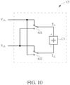
- FIG. 10 is a schematic diagram of the load circuit C5 according to an embodiment of the present application.
- Operations of the load circuit C5 is similar to operations of the polarity toggle module 62 shown in FIG. 10 of US Application No. 17/022,060 .
- > V SS and the input signal indicating V C3 is to be positive a first terminal of the capacitive load C3 (denoted as T 1L in FIG. 10 ) is connected to a first node (i.e. a positive terminal of the load circuit C5 with V C5+ ) by a toggle switch 621, and a second terminal of the capacitive load C3 (denoted as T 2L in FIG.
- a toggle switch 622 When
- the second node (i.e. V C5- ) of the load circuit C5 is connected to the source voltage V DD by setting the single-pole-dual-throw (SPDT) switch T5 to an S position (stands for small voltage swing).
- the bidirectional circuit 400 operates like a single ended amplifier with the V C5- terminal of the load circuit C5 fixed at the source voltage V DD while the voltage of the V C5+ (Vout) terminal of the load circuit C5 may swing above, below and across the source voltage level of the terminal V C5- of C5, connected to V DD .
- the bidirectional circuit 400 will assume the state 410.S1 and, under the control of the signal S1, electrical energy from the source voltage V DD will be stored as magnetic flux energy in the inductor L1.
- the bidirectional circuit 400 will assume the state 410.S2 and, under the control of the signal S2, the magnetic flux energy stored in the inductor L1 will be transferred to the load circuit C5 as electrical energy.
- the body diode of the switch T3 of FIG. 6 should be oriented such that the current may flow from the inductor L1 to the load circuit C5, but not inversely.
- the bidirectional circuit 400 During the 1st flux-increasing phase of the discharging (recycling) operation, the bidirectional circuit 400 will assume the state 415.S1 and, under the control of signals for the switches T1-T4, electrical energy from the load circuit C5 will be stored as magnetic flux energy in the inductor L1. During the 2nd flux-decreasing phase of the discharging (recycling) operation, the bidirectional circuit 400 will assume the state 415.S2 and, under the control of signals for the switches T1-T4, the magnetic flux energy stored in the inductor L1 will be transferred back to the voltage power source V DD as electrical energy.
- the body diode of the switch T1 of FIG. 7 should be oriented such that the current may flow from the inductor L1 to the voltage power source V DD , but not inversely.
- the second node (i.e. V C5- ) of the load circuit C5 is connected to the ground by the setting single-pole-dual-throw (SPDT) switch T5 to an L position (stands for large voltage swing).
- the bidirectional circuit 400 will produce a driving waveform that is similar to a BTL amplifier where the "-" terminal T 2L and the "+” terminal T 1L of the capacitive load C3 will take turn to be connected, through the toggle switch 621 (or 622) to the output voltage Vout of the bidirectional circuit 400, producing the voltage V C5 , while the other terminal is connected, through the toggle switch 622 (or 621) to the ground.
- the bidirectional circuit 400 will assume the state 420.S1 and, under the control of the signal S1, electrical energy from voltage source with the source voltage V DD will be stored as magnetic flux energy in the inductor L1.
- the bidirectional circuit 400 will assume the state 420.S2 and, under the control of the signal S2, the magnetic flux energy stored in the inductor L1 will be transferred to the load circuit C5 as electrical energy. Note that, as in the case of the state 120 or 121 and as illustrated in the pop out 122, the body diode of the switch T3 should be oriented such that the current may flow from the inductor L1 to the load circuit C5, but not inversely.
- the bidirectional charging and discharging circuit 400 will assume the state 425.S1 and, under the control of signals for the switches T1-T4, electrical energy from the load circuit C5 will be stored as magnetic flux energy in the inductor L1.
- the bidirectional circuit 400 will assume the state 425.S2 and, under the control of signals for the switches T1-T4, the magnetic flux energy stored in the inductor L1 will be transferred back to the source voltage V DD as electrical energy.
- the body diode of the switch T1 should be oriented such that the current may flow from the inductor L1 to the source voltage V DD , but not inversely.
- FIG. 12 illustrates a plot of an inductor current flowing through the inductor L1 versus time t .
- I pk represents a peak current of the inductor current
- Q represent a specific amount of electronic charges needed to be poured into (or drained from) the capacity load C3.
- T C,INFX and T C,DEFX denote the InFlux phase and the DeFlux phase of the charging operation; while T R,INFX and T R,DEFX denote the InFlux phase and the DeFlux phase of the recycling operation.
- T C,DEFX if the period of the T C,DEFX is lengthened (e.g., T C,DEFX > T C,INFX ), as top portion of FIG. 12 shows, a low value of peak current I pk can be exploited to charge the capacity load C3 to a certain amount/degree for the charging operation, such that conduction loss and power consumption can be reduced.
- T R,INFX may be lengthened (e.g., T R,INFX > T R,DEFX ) and similar rationale may be applied for the recycling operation, as bottom portion of FIG. 12 shows.
- the second terminal of the switch T2 may receive a (positive) voltage V BAT , instead of connected/coupled to the ground (as shown in FIG. 11 ), for the charging operation.
- the second terminal of the switch T4 may receive a (positive) voltage V BAT ', instead of being connected/coupled to the ground (as shown in FIG. 11 ).
- V BAT and V BAT ' may or may not be the same, depending on practical situation.
- FIG. 13 illustrates a bidirectional circuit 900 according to an embodiment of the present application.
- the bidirectional circuit 900 further comprises switches T2' and T4', controlled by PWM signals SP2' and SP4', respectively.
- First terminals of the switches T2' and T4' are coupled to the inductor L1.
- Second terminals of the switches T2' and T4' receives V BAT and V BAT ', respectively.
- the present application provides the bidirectional circuit for a capacitive load of a piezo speaker, which may be applied for a situation that the load voltage may swing both above and below the voltage level of the source voltage.
- the present application further provides a bidirectional circuit with a mixed mode solution by applying single-end configuration for smaller signal swings while switching to BTL configuration for larger signal swings, to achieve both the lower-distortion of the single-end configuration and the doubling of output voltage range of BTL configuration.
Landscapes
- Engineering & Computer Science (AREA)
- Power Engineering (AREA)
- Physics & Mathematics (AREA)
- Multimedia (AREA)
- General Engineering & Computer Science (AREA)
- Computing Systems (AREA)
- Computer Hardware Design (AREA)
- Mathematical Physics (AREA)
- Signal Processing (AREA)
- Acoustics & Sound (AREA)
- Microelectronics & Electronic Packaging (AREA)
- Dc-Dc Converters (AREA)
- Amplifiers (AREA)
Abstract
A driving circuit (70) is configured to drive a capacitive load (C3), and includes a bidirectional circuit (100) and a pulse width modulation (PWM) controller (76). The bidirectional circuit is coupled between a voltage source (11) and the capacitive load, and includes a first switch (T1), comprising a first terminal coupled to the voltage source; a second switch (T2), comprising a first terminal coupled to a second terminal of the first switch; an inductor (LI), comprising a first terminal coupled to the second terminal of the first switch and the first terminal of the second switch; a third switch (T3), comprising a first terminal coupled to a second terminal of the inductor, and a second terminal coupled to a first terminal of the capacitive load; and a fourth switch (T4), comprising a first terminal coupled to the second terminal of the inductor and the first terminal of the third switch.
Description
- The present application relates to a driving circuit, and more particularly, to a driving circuit capable of energy recycling.
- Recently, piezoelectric-actuated speakers (piezo-speakers) have emerged. Due to the capacitive nature of thin film piezoelectric actuators, these piezo-speakers present highly capacitive loads to the amplifiers. However, conventional driving circuits, such as class-AB, -D, -G, -H amplifiers, have all evolved assuming the loading (coils made of very fine wires) will be mostly resistive and slightly inductive; these amplifiers are inefficient when driving the highly capacitive loads such as piezo-speakers.
- In addition, due to the capacitive nature of the load, the current and driving voltage would be about 90° out of phase. As a result, piezo-speakers do not actually consume much of the power during the charging operation (or cycle). Most of the energy drawn during the charging phase is stored inside the capacitance of the load. However, during the recycling/discharging operation (or cycle), when the voltage across the speaker terminals decreases, conventional class-AB, -D, -G or -H amplifiers will simply drain the energy from the capacitance of the load to the ground (or to the negative power supply), which is wasted.
- Therefore, it is necessary to improve the prior art.
- It is therefore a primary objective of the present application to provide a driving circuit capable of energy recycling, to improve over disadvantages of the prior art.
- This is achieved by a driving circuit according to the independent claim 1 here below. The dependent claims pertain to corresponding further developments and improvements.
- As will be seen more clearly from the detailed description following below, an embodiment of the present application discloses a driving circuit, configured to drive a capacitive load according to an input signal, the driving circuit comprising a bidirectional circuit, coupled between a voltage source and the capacitive load, wherein the bidirectional circuit is configured to form a first current from the voltage source to the capacitive load when performing a charging operation and form a second current from the capacitive load to the voltage source when performing a recycling operation, the bidirectional circuit comprising a first switch, comprising a first terminal coupled to the voltage source, and a second terminal; a second switch, comprising a first terminal coupled to the second terminal of the first switch, and a second terminal; an inductor, comprising a first terminal coupled to the second terminal of the first switch and the first terminal of the second switch, and a second terminal; a third switch, comprising a first terminal coupled to the second terminal of the inductor, and a second terminal coupled to a first terminal of the capacitive load; and a fourth switch, comprising a first terminal coupled to the second terminal of the inductor and the first terminal of the third switch, and a second terminal; a pulse width modulation (PWM) controller, receiving the input signal and coupled to the capacitive load so as to receive an output signal of the capacitive load, configured to generate a plurality of PWM signals according to the input signal and the output signal; wherein the first switch, the second switch, the third switch and the fourth switch are controlled by the plurality of PWM signals generated by the PWM controller according to the input signal and the output signal, such that the output signal is substantially proportional to the input signal; wherein the input signal and the output signal are time varying signal.
-
-
FIG. 1 ,FIG. 2 ,FIG. 3 andFIG. 4 are schematic diagrams of a bidirectional circuit in different states according to an embodiment of the present application. -
FIG. 5 is a schematic diagram of a charging or recycling/discharging operation of the bidirectional circuit according to an embodiment of the present application. -
FIG. 6 ,FIG. 7 ,FIG. 8 andFIG. 9 are schematic diagrams of a bidirectional circuit in different states according to another embodiment of the present application. -
FIG. 10 is a schematic diagram of a load circuit according to an embodiment of the present application. -
FIG. 11 is a schematic diagram of a driving circuit according to an embodiment of the present application. -
FIG. 12 illustrates a plot of an inductor current flowing through the inductor versus time. -
FIG. 13 illustrates a bidirectional circuit according to an embodiment of the present application. - In the present application, the term "coupled to" may refer to direct or indirect connection. "Component A being coupled to component B" may indicate that component A is directly connected to component B or component A is connected to component B via some component C.
- To recycle the energy stored in the capacitive load, Applicant provides a driving circuit with energy recycle capability in
US Application No. 17/022,060 - In
US Application No. 17/022,060 - Therefore, the present application provides a bidirectional circuit for a capacitive load of a piezo speaker, where the load/output voltage may swing above, below and across the voltage level of the power source.
- In another aspect, just like a class-B amplifier, some BTL-like (BTL: bridge-tied-load) circuits in
US Application No. 17/022,060 -
FIG. 11 is a schematic diagram of adriving circuit 70 according to an embodiment of the present application. Thedriving circuit 70 comprises a pulse width modulation (PWM)controller 76 and abidirectional circuit 100. Thebidirectional circuit 100 is coupled between a voltage (power)source 11 and a capacitive load C3 (where the capacitive load C3 may comprise a piezo speaker), and configured to drive the capacitive load C3. Specifically, thebidirectional circuit 100 forms/drives a first current from thevoltage source 11 to the capacitive load C3 when performing a charging operation, and forms/drains a second current from the capacitive load C3 to thevoltage source 11 when performing a recycling operation. - The
bidirectional circuit 100 includes switches T1-T4 and an inductor L1. The switch T1 includes a first terminal coupled to thevoltage source 11. The switch T2 includes a first terminal coupled to the second terminal of the switch T1, and a second terminal coupled to a ground (in the embodiment shown inFIG. 11 , but not limited thereto). The inductor L1 includes a first terminal coupled to the second terminal of the switch T1 and the first terminal of the switch T2. The switch T3 includes a first terminal coupled to the second terminal of the inductor L1, and a second terminal coupled to a first terminal of the capacitive load C3. The switch T4 includes a first terminal coupled to the second terminal of the inductor L1 and the first terminal of the switch T3, and a second terminal coupled to a ground (in the current embodiment shown inFIG. 11 , but not limited thereto). - The
PWM controller 76, receiving an input signal IN and coupled to the capacitive load C3, is configured to generate a plurality of PWM signals SP1-SP4, according to the input signal IN and an output signal Vout. The input signal IN may be an audio signal, which is time-varying. The PWM signals SP1-SP4 are configured to control the switches T1-T4, respectively, such that thebidirectional circuit 100 may perform the charging operation and perform the recycling operation. Thebidirectional circuit 100 may perform the charging and recycling operations within different switching cycles. Via the charging and recycling operations (or by controlling the switches T1-T4 using the PWM signals SP1-SP4 the output signal Vout may be substantially proportional to the input signal IN, which means the output signal Vout is also time-varying. - In the present application, the output signal Vout being substantially proportional to the input signal IN implies that, ∥IN(t) - c·Vout(t)∥2 ≤ ε·∥IN(t)∥2 is satisfied, where ∥s(t)∥2 may represents an energy of an arbitrary signal s(t), IN(t) and Vout(t) represent time-varying function of the input signal and the output signal, respectively, c represents a constant which can be either positive or negative, and ε represent a small number which may be, e.g., 10-1, 10-2, 10-3 or less.
- In the present application the terms "output voltage" and "output signal" sometimes are used interchangeably. Both "output voltage" and "output signal" are denoted as Vout. When the term "output voltage" is used, it focuses more on certain (voltage) value at the first terminal of the capacitive load C3 within a specific time interval, e.g., within a switching cycle. When the term "output signal" is used, it addresses more on Vout as/being a time varying function. In other words, "output voltage" represents an instantaneous value of "output signal".
- Please refer to
FIG. 1 ,FIG. 2 ,FIG. 3 andFIG. 4 , which are schematic diagrams of thebidirectional circuit 100 instates - As shown in
FIG. 1 , thestates voltage power source 11 with a source voltage VDD into the inductor L1, in the form of magnetic flux, during a 1st flux-increasing phase of the charging operation of thebidirectional circuit 100. As shown inFIG. 2 , thestates bidirectional circuit 100. As shown inFIG. 3 , thestates bidirectional circuit 100. As shown inFIG. 4 , thestates voltage power source 11 during a 2nd flux-decreasing phase of the discharging (recycling) operation of thebidirectional circuit 100. - In the present application, flux-increasing phase is also known as InFlux phase, and the terms of "flux-increasing phase" and "InFlux phase" may be used interchangeably. Similarly, flux-decreasing phase is also known as DeFlux phase, and the terms of "flux-decreasing phase" and "DeFlux phase" may be used interchangeably.
- In detail, as shown in
FIG. 1 , thestates bidirectional circuit 100, wherein the switches T1, T4 are conducted in thestate 110 and the switches T1, T3 are conducted in thestate 111. During the 1st flux-increasing phase of charging operation, energy is stored into the inductor L1 in the form of magnetic flux and current flow. The amount of energy store in the inductor L1 at the end of this phase and its relationship to the voltage applied across the terminals of inductor L1 and the pulse width of the PWM control signal are described in Eq.1 and Eq.2 below. - The formula describing the energy stored in the inductor L1 is given as below:

- The energy transferred from a voltage VL to the inductor L1 can be calculated as:

- When the source voltage VDD is higher than a output voltage Vout at the first terminal of the capacitive load C3 by a sufficient/specific margin, e.g. VDD - Vout > VM, where VM represents a margin (in voltage) and may range from 1.2 V to 1.5V or be 1V, but not limited thereto, the
state 111 of thebidirectional circuit 100 may be more efficient than thestate 110 due to ability of thestate 111 to lower the current flowing through thebidirectional circuit 100, which lowers the conduction loss due to the unavoidable resistances of the inductor L1 and the switches T1-T4. However, when the source voltage VDD is not higher than the output voltage Vout by the sufficient/specific margin, e.g. VDD - Vout < VM, the duration tPWM required to store a given amount of energy E into the inductor L1 in thestate 111 may increase rapidly since the voltage VL, as expressed in Eq.2, is small (VL- VDD - Vout in the state 111), potentially causing the operation of thestate 111 to fail. - Unlike the
state 111, thebidirectional circuit 100 in thestate 110 can handle all conditions of the output voltage Vout because, when in the 1st flux-increasing phase of charging operation in thestate 110, the value of the voltage VL across the inductor L1 in Eq.2 always equals the source voltage VDD. Therefore, as can be derived from Eq.2, the duration tPWM required to store a given among of energy E into the inductor L1 will be constant, independent of the value of the output voltage Vout. Therefore, the use of thestate 111 is optional when the source voltage VDD is higher than the output voltage Vout by a sufficient margin, or VDD - VM > Vout, and higher efficiency is desirable, while the use of thestate 110 is a must for the output voltage Vout > VDD -VM. - As shown in
FIG. 2 , thestates bidirectional circuit 100, wherein the switches T2, T3 are conducted in thestate 120 and the switches T1, T3 are conducted in thestate 121. During the 2nd flux-decreasing phase of charging operation, the magnetic flux energy stored in the inductor L1 is transferred, via current flow, to the capacitive load C3 as electrical charge. During this phase, the switch T3, along with its body diode, allows the current to flow only from the inductor L1 toward the capacitive load C3, and is turned off (in "nonconducting" state) when the current of the inductor L1 diminishes to 0, following a style commonly referred to as synchronous mode switching in the field of DC-DC power conversion, by employing a zero-current-detection (ZCD) or zero-current-estimation (ZCE) circuit to generate the control signal of the switch T3. - Furthermore, the switches T1∼T4 may implemented as MOSFET with embedded body-diodes. When the body diode of such MOSFET switch T3 is oriented from the inductor L1 toward the capacitive load C3, as indicated in a pop-out 122, then even if the switch T3 is not turned ON the function of directing the current to flow from the inductor L1 toward the capacitive load C3 (but not inversely), operations may still be performed correctly, albeit less efficiently (due to the high forward voltage drop over such body-diode). The existence of such body diode allows the width of the PWM control signal of the switch T3 to be narrower than would be required otherwise.
- For most combinations of the source voltage VDD and the output voltage Vout, the 2nd flux-decreasing phase of the charging operation of the
bidirectional circuit 100 may be performed under thestate 120. However, when the output voltage Vout is higher than the source voltage VDD by a significant margin, e.g. Vout > VDD + VM, where VM may be 3V but not limited thereto, thestate 121 ofcircuit 100 may be preferable to thestate 120 due to its ability to avoid the PWM pulse width becoming too narrow when the level of Vout rises by changing the PWM pulse width of the 2nd flux-decreasing phase, as expressed by Eq.2 from

- Note that although connection configurations of the switches T1-T4 in the
state 111 and thestate 121 are the same, these two states however are actually meant for two completely different situations: the state 101 is for 1st flux-increasing phase (or InFlux phase) of charging operation when the source voltage VDD is higher than the output voltage/signal Vout by a sufficient/specific margin, e.g. VDD > Vout + 1V, while thestate 121 is for 2nd flux-decreasing phase of charging operation when the output voltage Vout is higher than the source voltage VDD by a sufficient/specific margin, e.g. Vout > VDD + 3V. So, it will never occur where same connection scheme is employed both during the 1st flux-increasing phase and during the 2nd flux-decreasing phase of the charging operation of thebidirectional circuit 100. - Please refer to
FIG. 5 , which is a control signal timing diagram of a charging or recycling/discharging operation of thebidirectional circuit 100 according to an embodiment of the present application, wherein a signal S1 is the control signal for switches (T1-T4) to be turned ON during the 1st flux-increasing phase and a signal S2 is the control signal for switches to be turned ON during the 2nd flux-decreasing phase. The signals S1 and S2 may schematically illustrate the PWM signals SP1-SP4 shown inFIG. 11 . - For example, at t = t0, the 1st flux-increasing phase of the charging operation of the
bidirectional circuit 100 starts by turning ON (put into "conducting" states) the switches T1 and T4 to activate thestate 110 or by turning ON the switches T1 and T3 to activate thestate 111. The magnitude of current |IL1 | in the inductor L1 will rise from 0 according to formula:

bidirectional circuit 100 transitions into the 2nd flux-decreasing phase by turning OFF the switches T1 and T4 (or T1 and T3) and turning ON the switches T2 and T3 (or T1 and T3) to activate the state 120 (or the state 121) of thebidirectional circuit 100, directing the inductor current |IL1| generated during the 1st flux-increasing phase toward capacitive load C3. The output voltage/signal Vout causes the inductor current |IL1| to fall back to 0 during the 2nd flux-decreasing phase and the magnetic flux energy stored in the inductor L1 is transferred into electric charge Q stored capacitive load C3 of the piezo speaker, resulting in rise of the voltage VC3 across the two terminals of the capacitive load C3, i.e. the voltage VC3 rises from V1 to V2. Toward the end of the charging operation, a zero current detection circuit will turn OFF the switch T3 when the inductor current |IL1| approaches 0. - It is conventional to insert a "dead time" between the ON period of the signal S1 and the ON period of the signal S2, as indicated by the small gap on the left side of the ON period of the signal S2. On the right side of the ON period of the signal S2 another small gap is shown before the current in the inductor L1 actually returns to 0. As discussed in a prior paragraph, during either of these two time gaps, by orienting body-diode of the switch T3 properly as illustrated in the pop-out 122, the current in the inductor L1 will flow correctly in both the
states - Noticeably, recycling/discharging operations of the
states FIG. 3 andFIG. 4 may be derived by referring to charging operations of thestates FIG. 1 ,FIG. 2 as operations in a reverse direction, and are not narrated herein for brevity. - The
bidirectional circuit 100 works well for application where the output voltage/signal Vout needs not swing very close to 0V. However, when the output voltage/signal Vout falls below a threshold voltage, such as Vout < 0.7V, the required ON period (i.e. the duration tPWM) during the operations of both thestate 120 and thestate 210 will start to increase rapidly. Therefore, thebidirectional circuit 100 is best suited for situations where the output voltage Vout swings above 0V by a significant margin, but not suited for situations where the output voltage Vout needs to swing close to, or across, 0V - Please refer to
FIG. 6 ,FIG. 7 ,FIG. 8 andFIG. 9 , which are schematic diagrams of abidirectional circuit 400 in states 410.S1, 410.S2, 415.S1, 415.S2, 420.S1, 420.S2, 425.S1, 425.S2 according to an embodiment of the present application. Thebidirectional circuit 400 is similar to thebidirectional circuit 100, and elements with similar functions are denoted by the same symbols for simplicity. A main difference is that thebidirectional circuit 400 operates in a dual-mode, and includes a switch T5 and a load circuit C5 containing the capacitive load C3. - In detail, the four states 410.S1, 410.S2, 415.S1 and 415.S2 shown in
FIG. 6 ,FIG. 7 are for conditions where the magnitude of voltage VC5 across a load circuit C5 is less than a threshold voltage VSS, i.e. |VC5| < VSS, where the threshold voltage VSS may equal the source voltage VDD subtracting a modest margin, e.g. VSS = VDD-VM where VM may be 1.5V but not limited thereto, while the four states 420.S1, 420.S2, 425.S1 and 425.S2 inFIG. 8 andFIG. 9 are for conditions where the magnitude of voltage VC5 across the load circuit C5 is greater than the threshold voltage VSS, |VC5| > VSS, where the voltage VC5 is the voltage across the load circuit C5, i.e. VC5= VC5+- VC5-. For example, if VDD =5V and VM=1.5V then VSS =3.5V, the four states 410.S1, 410.S2, 415.S1 and 415.S2 shown inFIG. 6 ,FIG. 7 are applicable for -3.5V < VC5< 3.5V while the four states 420.S1, 420.S2, 425.S1 and 425.S2 inFIG. 8 andFIG. 9 are applicable for either VC5> 3.5V or VC5< -3.5V - Please refer to
FIG. 10 , which is a schematic diagram of the load circuit C5 according to an embodiment of the present application. Operations of the load circuit C5 is similar to operations of the polarity toggle module 62 shown inFIG. 10 ofUS Application No. 17/022,060 FIG. 10 ) is connected to a first node (i.e. a positive terminal of the load circuit C5 with VC5+) by atoggle switch 621, and a second terminal of the capacitive load C3 (denoted as T2L inFIG. 10 ) is connected to a second node (i.e. a negative terminal of the load circuit C5 with VC5-) by atoggle switch 622. When |VC5| > VSS and the input signal indicating VC3 is to be negative, the first terminal T1L is connected to the second node (VC5-) by thetoggle switch 621, and the second terminal T2L is connected to the first node (VC5+) by thetoggle switch 622. - Please refer back to
FIG. 6 ,FIG. 7 , when |VC5| < VSS, the second node (i.e. VC5-) of the load circuit C5 is connected to the source voltage VDD by setting the single-pole-dual-throw (SPDT) switch T5 to an S position (stands for small voltage swing). During this mode, thebidirectional circuit 400 operates like a single ended amplifier with the VC5- terminal of the load circuit C5 fixed at the source voltage VDD while the voltage of the VC5+ (Vout) terminal of the load circuit C5 may swing above, below and across the source voltage level of the terminal VC5- of C5, connected to VDD. - During the 1st flux-increasing phase of the charging operation, the
bidirectional circuit 400 will assume the state 410.S1 and, under the control of the signal S1, electrical energy from the source voltage VDD will be stored as magnetic flux energy in the inductor L1. During the 2nd flux-decreasing phase of the charging operation, thebidirectional circuit 400 will assume the state 410.S2 and, under the control of the signal S2, the magnetic flux energy stored in the inductor L1 will be transferred to the load circuit C5 as electrical energy. Note that, same as in the case of thestate FIG. 6 should be oriented such that the current may flow from the inductor L1 to the load circuit C5, but not inversely. - During the 1st flux-increasing phase of the discharging (recycling) operation, the
bidirectional circuit 400 will assume the state 415.S1 and, under the control of signals for the switches T1-T4, electrical energy from the load circuit C5 will be stored as magnetic flux energy in the inductor L1. During the 2nd flux-decreasing phase of the discharging (recycling) operation, thebidirectional circuit 400 will assume the state 415.S2 and, under the control of signals for the switches T1-T4, the magnetic flux energy stored in the inductor L1 will be transferred back to the voltage power source VDD as electrical energy. Note that, same as in the case of thestate FIG. 7 should be oriented such that the current may flow from the inductor L1 to the voltage power source VDD, but not inversely. - Note that, the previously discussed rapid rise of the required ON period (i.e. the duration tPWM) in
state 120 andstate 210 ofcircuit 100 when the voltage across terminals of C3 (Vout) is at or near 0V, since such condition fulfills the |VC5| < VSS criteria, is avoided incircuit 400 by the raising the output voltage Vout (VC5+), together with VC5-, to VDD where
circuit 400 overcircuit 100. - When |VC5| > VSS, the second node (i.e. VC5-) of the load circuit C5 is connected to the ground by the setting single-pole-dual-throw (SPDT) switch T5 to an L position (stands for large voltage swing). During this mode, the
bidirectional circuit 400 will produce a driving waveform that is similar to a BTL amplifier where the "-" terminal T2L and the "+" terminal T1L of the capacitive load C3 will take turn to be connected, through the toggle switch 621 (or 622) to the output voltage Vout of thebidirectional circuit 400, producing the voltage VC5, while the other terminal is connected, through the toggle switch 622 (or 621) to the ground. - During the 1st flux-increasing phase of the charging operation, the
bidirectional circuit 400 will assume the state 420.S1 and, under the control of the signal S1, electrical energy from voltage source with the source voltage VDD will be stored as magnetic flux energy in the inductor L1. During the 2nd flux-decreasing phase of the charging operation, thebidirectional circuit 400 will assume the state 420.S2 and, under the control of the signal S2, the magnetic flux energy stored in the inductor L1 will be transferred to the load circuit C5 as electrical energy. Note that, as in the case of thestate - During the 1st flux-increasing phase of the discharging operation, the bidirectional charging and discharging
circuit 400 will assume the state 425.S1 and, under the control of signals for the switches T1-T4, electrical energy from the load circuit C5 will be stored as magnetic flux energy in the inductor L1. During the 2nd flux-decreasing phase of the discharging operation, thebidirectional circuit 400 will assume the state 425.S2 and, under the control of signals for the switches T1-T4, the magnetic flux energy stored in the inductor L1 will be transferred back to the source voltage VDD as electrical energy. Note that, as in the case of thestate - Normally, the flux-increasing phase and the flux-decreasing phase in the charging operation or the recycling operation may be in a symmetric manner. However, in order to reduce conduction loss and power consumption, in an embodiment, the flux-increasing phase and the flux-decreasing phase in the charging operation or the recycling operation may be in an asymmetric manner.
FIG. 12 illustrates a plot of an inductor current flowing through the inductor L1 versus time t. Ipk represents a peak current of the inductor current, Q represent a specific amount of electronic charges needed to be poured into (or drained from) the capacity load C3. TC,INFX and TC,DEFX denote the InFlux phase and the DeFlux phase of the charging operation; while TR,INFX and TR,DEFX denote the InFlux phase and the DeFlux phase of the recycling operation. Symmetric manner means TC,INFX = TC,DEFX and TR,INFX = TR,DEFX; while asymmetric manner means TC,INFX ≠ TC,DEFX and TR,INFX ≠ TR,DEFX. - As can be shown in
FIG. 12 , if the period of the TC,DEFX is lengthened (e.g., TC,DEFX> TC,INFX), as top portion ofFIG. 12 shows, a low value of peak current Ipk can be exploited to charge the capacity load C3 to a certain amount/degree for the charging operation, such that conduction loss and power consumption can be reduced. Similarly, TR,INFX may be lengthened (e.g., TR,INFX> TR,DEFX) and similar rationale may be applied for the recycling operation, as bottom portion ofFIG. 12 shows. - It can be achieved by 1) lowering the voltage difference between the two terminals of the inductor L1; and 2) designing the PWM signals (e.g., SP3 and SP2) such that TC,DEFX> TC,INFX or TR,INFX> TR,DEFX may be achieved.
- To achieve item 1) in the above, the second terminal of the switch T2 may receive a (positive) voltage VBAT, instead of connected/coupled to the ground (as shown in
FIG. 11 ), for the charging operation. On the other hand, for the recycling operation, the second terminal of the switch T4 may receive a (positive) voltage VBAT', instead of being connected/coupled to the ground (as shown inFIG. 11 ). VBAT and VBAT' may or may not be the same, depending on practical situation. -
FIG. 13 illustrates abidirectional circuit 900 according to an embodiment of the present application. In addition to thebidirectional circuit 100, thebidirectional circuit 900 further comprises switches T2' and T4', controlled by PWM signals SP2' and SP4', respectively. First terminals of the switches T2' and T4' are coupled to the inductor L1. Second terminals of the switches T2' and T4' receives VBAT and VBAT', respectively. By properly designing the PWM signals SP1-SP4, SP2' and SP4', (a)symmetric manner of InFlux versus DeFlux may be achieved. In the present application, symmetric manner indicates InFlux time and Deflux time are the same, while asymmetric manner indicates InFlux time and Deflux time are different. - To sum up, the present application provides the bidirectional circuit for a capacitive load of a piezo speaker, which may be applied for a situation that the load voltage may swing both above and below the voltage level of the source voltage. Besides, the present application further provides a bidirectional circuit with a mixed mode solution by applying single-end configuration for smaller signal swings while switching to BTL configuration for larger signal swings, to achieve both the lower-distortion of the single-end configuration and the doubling of output voltage range of BTL configuration.
Claims (15)
- A driving circuit (70), configured to drive a capacitive load (C3) according to an input signal (IN), characterised by, the driving circuit (70) comprising:a bidirectional circuit (100), coupled between a voltage source (11) and the capacitive load (C3), wherein the bidirectional circuit (100) is configured to form a first current from the voltage source (11) to the capacitive load (C3) when performing a charging operation and form a second current from the capacitive load (C3) to the voltage source (11) when performing a recycling operation, the bidirectional circuit (100) comprising:a first switch (T1), comprising a first terminal coupled to the voltage source (11), and a second terminal;a second switch (T2), comprising a first terminal coupled to the second terminal of the first switch (T1), and a second terminal;an inductor (L1), comprising a first terminal coupled to the second terminal of the first switch (T1) and the first terminal of the second switch (T2), and a second terminal;a third switch (T3), comprising a first terminal coupled to the second terminal of the inductor (L1), and a second terminal coupled to a first terminal of the capacitive load (C3); anda fourth switch (T4), comprising a first terminal coupled to the second terminal of the inductor (L1) and the first terminal of the third switch (T3), and a second terminal;a pulse width modulation (PWM) controller (76), receiving the input signal (IN) and coupled to the capacitive load (C3) so as to receive an output signal (Vout) of the capacitive load (C3), configured to generate a plurality of PWM signals (SP1-SP4) according to the input signal (IN) and the output signal (Vout);wherein the first switch (T1), the second switch (T2), the third switch (T3) and the fourth switch (T4) are controlled by the plurality of PWM signals (SP1-SP4) generated by the PWM controller (76) according to the input signal (IN) and the output signal (Vout), such that the output signal (Vout) is substantially proportional to the input signal(IN);wherein the input signal(IN) and the output signal are time varying signal.
- The driving circuit (70) of claim 1, characterised in that, the first switch (T1) and the fourth switch (T4) are conducted during a first phase of the charging operation; or
when a source voltage (VDD) of the voltage source (11) is higher than the output signal (Vout) at the first terminal of the capacitive load (C3) by a specific margin, the first switch (T1) and the third switch (T3) are conducted during the first phase of the charging operation. - The driving circuit (70) any of claims 1-2, characterised in that,
the second switch (T2) and the third switch (T3) are conducted during a second phase of the charging operation; or
when the output signal (Vout) at the first terminal of the capacitive load (C3) is significant higher than a source voltage (VDD) of the voltage source (11), the first switch (T1) and the third switch (T3) are conducted during the second phase of the charging operation. - The driving circuit (70) any of claims 1-3, characterised in that,
the second switch (T2) and the third switch (T3) are conducted during a first phase of the recycling operation; or
when a source voltage (VDD) of the voltage source (11) is lower than the output signal (Vout) at the first terminal of the capacitive load (C3) by a specific margin, the first switch (T1) and the third switch (T3) are conducted during the first phase of the recycling operation. - The driving circuit (70) any of claims 1-4, characterised in that,
the first switch (T1) and the fourth switch (T4) are conducted during a second phase of the recycling operation; or
when a source voltage (VDD) of the voltage source (11) is significant higher than the output signal (Vout) at the first terminal of the capacitive load (C3), the first switch (T1) and the third switch (T3) are conducted during the second phase of the recycling operation. - The driving circuit (70) any of claims 1-5, characterised in that,
the third switch (T3) is conducted during a second phase of the charging operation and is turned off when a current of the inductor (L1) diminishes to zero; or
the first switch (T1) is conducted during a second phase of the recycling operation and is turned off when a current of the inductor (L1) diminishes to zero. - The driving circuit (70) any of claims 1-6, characterised in that,
the third switch (T3) is a MOSFET (Metal-Oxide-Semiconductor Field-Effect Transistor), and a body diode of the third switch (T3) is pointed from the inductor (L1) toward the capacitive load (C3); or
the first switch (T1) is a MOSFET, and a body diode of the first switch (T1) is pointed from the inductor (L1) toward the voltage source (11). - The driving circuit (70) any of claims 1-7, characterised in that, the bidirectional circuit (100) further comprises:a fifth switch (T5), connected to the voltage source (11), a load circuit (C5) and a ground;wherein the load circuit (C5) comprises the capacitive load (C3), a first node and a second node connected to the fifth switch (T5);wherein
when a magnitude of a voltage (VC5) across the first node and the second node of the load circuit (C5) is less than a threshold voltage, the fifth switch (T5) conducts a connection between the source voltage (VDD) and the second node of the load circuit (C5); or
when the magnitude of the voltage (VC5) across the first node and the second node is greater than the threshold voltage, the fifth switch (T5) conducts a connection between the second node and the ground. - The driving circuit (70) of claim 8, characterised in that, the load circuit (C5) comprises:a first toggle switch (621), connected to the first terminal of the capacitive load (C3), the first node and the second node; anda second toggle switch (622), connected to the second terminal of the capacitive load (C3), the first node and the second node.
- The driving circuit (70) of claim 9, characterised in that,
when the input signal (IN) indicates that a voltage (VC3) across the capacitive load (C3) is to be positive, the first toggle switch (621) conducts a connection between the first terminal of the capacitive load (C3) and the first node, and the second toggle switch (622) conducts a connection between the second terminal of the capacitive load (C3) and the second node;
when the input signal (IN) indicates that the voltage (VC3) across the capacitive load (C3) is to be negative, the first toggle switch (621) conducts a connection between the first terminal of the capacitive load (C3) and the second node, and the second toggle switch (622) conducts a connection between the second terminal of the capacitive load (C3) and the first node. - The driving circuit (70) any of claims 1-10, characterised in that, during a flux-decreasing phase of the charging operation or during a flux-increasing phase of the recycling operation, a voltage difference between the first and the second terminals of the inductor (L1) is less than the output signal (Vout).
- The driving circuit (70) of claim 11, characterised in that, the second terminal of the second switch (T2 or T2') receives a first voltage (VBAT) during a flux-decreasing phase of the charging operation or the second terminal of the fourth switch (T4 or T4') receives a second voltage (VBAT') during a flux-increasing phase of the recycling operation, such that the voltage difference between the first and the second terminals of the inductor (L1) is less than the output signal (Vout).
- The driving circuit (70) of claim 12, characterised in that, the bidirectional circuit (100) comprises:a sixth switch (T2'), controlled by a PWM signal (SP2') generated by the PWM controller (76), comprising a first terminal coupled to the first terminal of the inductor (L1), and a second terminal;wherein the second terminal of the second switch (T2) is coupled to a ground;wherein the second terminal of the sixth switch (T2') receives the first voltage (VBAT).
- The driving circuit (70) of claim 12, characterised in that, the bidirectional circuit (100) comprises:a seventh switch (T4'), controlled by a PWM signal (SP4') generated by the PWM controller (76), comprising a first terminal coupled to the second terminal of the inductor (L), and a second terminal;wherein the second terminal of the fourth switch (T4) is coupled to a ground;wherein the second terminal of the seventh switch (T4') receives the second voltage (VBAT').
- The driving circuit (70) any of claims 1-14, characterised in that,
the plurality of the PWM signals (SP1-SP4, SP2', SP4') is generated such that for the charging operation, a first duration of a flux-increasing phase of the charging operation is less than or equal to a second duration of a flux-decreasing phase of the charging operation; or
the plurality of the PWM signals (SP1-SP4, SP2', SP4') is generated such that for the recycling operation, a first duration of a flux-increasing phase of the recycling operation is longer than or equal to a second duration of a flux-decreasing phase of the recycling operation.
Applications Claiming Priority (3)
| Application Number | Priority Date | Filing Date | Title |
|---|---|---|---|
| US202063053662P | 2020-07-19 | 2020-07-19 | |
| US202063110051P | 2020-11-05 | 2020-11-05 | |
| US17/352,346 US11336182B2 (en) | 2020-07-19 | 2021-06-20 | Driving circuit with energy recycle capability |
Publications (1)
| Publication Number | Publication Date |
|---|---|
| EP3944494A1 true EP3944494A1 (en) | 2022-01-26 |
Family
ID=79293653
Family Applications (1)
| Application Number | Title | Priority Date | Filing Date |
|---|---|---|---|
| EP21184467.5A Withdrawn EP3944494A1 (en) | 2020-07-19 | 2021-07-08 | Driving circuit with energy recycle capability |
Country Status (4)
| Country | Link |
|---|---|
| US (1) | US11336182B2 (en) |
| EP (1) | EP3944494A1 (en) |
| KR (1) | KR102611844B1 (en) |
| CN (1) | CN114025284B (en) |
Families Citing this family (4)
| Publication number | Priority date | Publication date | Assignee | Title |
|---|---|---|---|---|
| US11775044B1 (en) * | 2022-04-01 | 2023-10-03 | ONiO AS | Energy recycling in an embedded system |
| CN119522536A (en) * | 2022-07-19 | 2025-02-25 | 华为技术有限公司 | Driving circuit and method for driving capacitive load, and speaker device and electronic device including the driving circuit |
| CN117477912A (en) * | 2022-07-20 | 2024-01-30 | 华为技术有限公司 | A driving circuit and switching power supply |
| US12270836B1 (en) * | 2023-11-03 | 2025-04-08 | xMEMS Labs, Inc. | Circuit and method of adjusting conduction period for energy-recycling circuit |
Citations (3)
| Publication number | Priority date | Publication date | Assignee | Title |
|---|---|---|---|---|
| JP2000333445A (en) * | 1999-05-21 | 2000-11-30 | Toyota Motor Corp | Bidirectional DC-DC converter |
| JP2013009176A (en) * | 2011-06-24 | 2013-01-10 | Asahi Kasei Electronics Co Ltd | Driving driver, driving amplifier and information apparatus |
| JP2013009179A (en) * | 2011-06-24 | 2013-01-10 | Asahi Kasei Electronics Co Ltd | Driving driver, driving amplifier and information apparatus |
Family Cites Families (32)
| Publication number | Priority date | Publication date | Assignee | Title |
|---|---|---|---|---|
| US5734258A (en) * | 1996-06-03 | 1998-03-31 | General Electric Company | Bidirectional buck boost converter |
| US7262979B2 (en) * | 2004-06-09 | 2007-08-28 | Yuan Ze University | Current source wave voltage inverter voltage-clamping and soft-switching techniques, and fuel cell system using the same |
| US7598792B2 (en) * | 2005-01-31 | 2009-10-06 | Queen's University At Kingston | Resonant gate drive circuits |
| TWI325675B (en) * | 2006-08-07 | 2010-06-01 | Addtek Corp | Dc/dc converter having auto auxiliary voltage supply and output fail protection |
| GB2479445B (en) * | 2006-08-31 | 2011-11-30 | Wolfson Microelectronics Plc | DC-DC converter circuits and methods and apparatus including such circuits |
| US8319483B2 (en) * | 2007-08-06 | 2012-11-27 | Solaredge Technologies Ltd. | Digital average input current control in power converter |
| WO2011010443A1 (en) | 2009-07-24 | 2011-01-27 | 旭化成エレクトロニクス株式会社 | Drive device |
| WO2012055968A1 (en) * | 2010-10-27 | 2012-05-03 | Merus Aps | Audio amplifier using multi-level pulse width modulation |
| US10381924B2 (en) | 2011-05-05 | 2019-08-13 | Psemi Corporation | Power converters with modular stages |
| US9048670B2 (en) | 2011-07-12 | 2015-06-02 | National Semiconductor Corporation | System and method for balancing electrical energy storage devices via differential power bus and capacitive load switched-mode power supply |
| US8896182B2 (en) | 2012-04-05 | 2014-11-25 | General Electric Corporation | System for driving a piezoelectric load and method of making same |
| CN104272589B (en) * | 2012-04-30 | 2017-10-24 | 梅鲁斯音频有限公司 | D audio frequency amplifier with adjustable loop filter characterization |
| KR101985934B1 (en) | 2012-11-23 | 2019-06-05 | 엘지디스플레이 주식회사 | DC-DC Converter Controlled by Pulse Width Modulation Manner |
| US9621108B2 (en) | 2013-01-14 | 2017-04-11 | Cognipower, Llc | Flyback amplifier with direct feedback |
| EP2763317A3 (en) | 2013-02-01 | 2014-10-15 | Rogers Corporation | Direct drive waveform amplifier |
| US9802493B2 (en) * | 2014-06-20 | 2017-10-31 | Cooper Technologies Company | Multi-phase bidirectional DC to DC power converter circuits, systems and methods with transient stress control |
| US9294000B1 (en) * | 2014-09-12 | 2016-03-22 | Texas Instruments Incorporated | Direct conversion output driver |
| GB2532725B (en) | 2014-11-24 | 2019-02-27 | Jaguar Land Rover Ltd | Vehicle electrical circuit protection |
| US9716433B2 (en) | 2015-01-15 | 2017-07-25 | R2 Semiconductor, Inc. | Control of conversion ratios of a power source block and a bidirectional active filter |
| US10050559B2 (en) | 2016-01-20 | 2018-08-14 | Linear Technology Llc | Control architecture with improved transient response |
| GB201602724D0 (en) | 2016-02-16 | 2016-03-30 | Nvf Tech Ltd | Switching amplifiers and power converters |
| CN115001250B (en) | 2016-04-01 | 2026-01-27 | 侯经权 | Direct drive power control |
| US10700589B2 (en) * | 2016-04-29 | 2020-06-30 | Massachusetts Institute Of Technology | Wide-operating-range resonant-transition soft-switched converter |
| US10284089B2 (en) | 2016-09-23 | 2019-05-07 | Apple Inc. | Integrated bi-directional driver with modulated signals |
| US10666145B2 (en) * | 2017-02-03 | 2020-05-26 | President And Fellows Of Harvard College | Highly integrated high voltage actuator driver |
| JP6693446B2 (en) | 2017-03-10 | 2020-05-13 | トヨタ自動車株式会社 | Drive |
| JP2019161689A (en) | 2018-03-07 | 2019-09-19 | ソニー株式会社 | Driving circuit, electronic device, and control method of driving circuit |
| US10484784B1 (en) * | 2018-10-19 | 2019-11-19 | xMEMS Labs, Inc. | Sound producing apparatus |
| US20200313567A1 (en) | 2018-11-14 | 2020-10-01 | Advanced Energy Industries, Inc. | Additive synthesis of interleaved switch mode power stages for minimal delay in set point tracking |
| US11418119B2 (en) * | 2019-05-21 | 2022-08-16 | Texas Instruments Incorporated | Wide switching frequency range switched mode power supply control topology |
| US11133784B2 (en) * | 2019-12-10 | 2021-09-28 | xMEMS Labs, Inc. | Method of driving circuit with energy recycle capability |
| DE102020133516A1 (en) * | 2019-12-24 | 2021-06-24 | Silicon Works Co., Ltd. | DOWN-UP CONVERTER CIRCUIT |
-
2021
- 2021-06-20 US US17/352,346 patent/US11336182B2/en active Active
- 2021-07-08 EP EP21184467.5A patent/EP3944494A1/en not_active Withdrawn
- 2021-07-14 CN CN202110794016.4A patent/CN114025284B/en active Active
- 2021-07-16 KR KR1020210093747A patent/KR102611844B1/en active Active
Patent Citations (3)
| Publication number | Priority date | Publication date | Assignee | Title |
|---|---|---|---|---|
| JP2000333445A (en) * | 1999-05-21 | 2000-11-30 | Toyota Motor Corp | Bidirectional DC-DC converter |
| JP2013009176A (en) * | 2011-06-24 | 2013-01-10 | Asahi Kasei Electronics Co Ltd | Driving driver, driving amplifier and information apparatus |
| JP2013009179A (en) * | 2011-06-24 | 2013-01-10 | Asahi Kasei Electronics Co Ltd | Driving driver, driving amplifier and information apparatus |
Non-Patent Citations (1)
| Title |
|---|
| HÄNSLER MARKUS ET AL: "Design of a MEMS speaker driver", ELEKTROTECHNIK UND INFORMATIONSTECHNIK, SPRINGER VERLAG, WIEN, AT, vol. 135, no. 1, 23 January 2018 (2018-01-23), pages 10 - 17, XP036438128, ISSN: 0932-383X, [retrieved on 20180123], DOI: 10.1007/S00502-018-0593-8 * |
Also Published As
| Publication number | Publication date |
|---|---|
| US11336182B2 (en) | 2022-05-17 |
| CN114025284B (en) | 2024-05-28 |
| KR20220010704A (en) | 2022-01-26 |
| US20220021304A1 (en) | 2022-01-20 |
| KR102611844B1 (en) | 2023-12-07 |
| CN114025284A (en) | 2022-02-08 |
Similar Documents
| Publication | Publication Date | Title |
|---|---|---|
| EP3944494A1 (en) | Driving circuit with energy recycle capability | |
| US6411153B2 (en) | Universal pulse width modulated zero voltage transition switching cell | |
| EP2618486B1 (en) | A method and apparatus for driving a voltage controlled power switch device | |
| CN100521473C (en) | Stepped inductor for fast transient response of switching converter | |
| US7859868B2 (en) | Synchronous rectifier control circuit with deadtime adjustment to prevent crossover conduction | |
| CN115868105A (en) | Soft switching pulse width modulation DC-DC power converter | |
| EP3883112B1 (en) | Acf converter, voltage conversion method and electronic device | |
| US6353543B2 (en) | Switching circuit of power conversion apparatus | |
| CN106941318A (en) | Power inverter | |
| CN110994982B (en) | A soft-switching BUCK converter and its control method | |
| JP4043321B2 (en) | Switching power supply | |
| US10348205B1 (en) | Coupled-inductor cascaded buck converter with fast transient response | |
| US8344762B2 (en) | Gate driving circuit | |
| US12261520B2 (en) | Zero current detector with pre-charge circuit | |
| KR102155031B1 (en) | Power supply and gate driver therein | |
| US20250247020A1 (en) | Energy recovery driver for pzt actuators | |
| WO2003047103A1 (en) | Switch mode power supply and driving method for efficient rf amplification | |
| CN212258783U (en) | Direct current power conversion circuit | |
| EP1728321A1 (en) | Switch mode power supply with output voltage equalizer | |
| JP2009159696A (en) | Switching power supply | |
| CN115021578A (en) | Flyback converter control method and device and flyback converter | |
| CN102761260B (en) | With the booster circuit of low-voltage driving and correlation technique | |
| JP3306542B2 (en) | Partially Resonant Self-Excited Switching Power Supply Low Loss Circuit | |
| US20260088734A1 (en) | Converting device and method of controlling the same | |
| JP4970009B2 (en) | Gate drive circuit for switching element |
Legal Events
| Date | Code | Title | Description |
|---|---|---|---|
| PUAI | Public reference made under article 153(3) epc to a published international application that has entered the european phase |
Free format text: ORIGINAL CODE: 0009012 |
|
| STAA | Information on the status of an ep patent application or granted ep patent |
Free format text: STATUS: THE APPLICATION HAS BEEN PUBLISHED |
|
| AK | Designated contracting states |
Kind code of ref document: A1 Designated state(s): AL AT BE BG CH CY CZ DE DK EE ES FI FR GB GR HR HU IE IS IT LI LT LU LV MC MK MT NL NO PL PT RO RS SE SI SK SM TR |
|
| STAA | Information on the status of an ep patent application or granted ep patent |
Free format text: STATUS: THE APPLICATION IS DEEMED TO BE WITHDRAWN |
|
| 18D | Application deemed to be withdrawn |
Effective date: 20220727 |