EP3944350A1 - Photoelectric conversion element and method for manufacturing photoelectric conversion element - Google Patents
Photoelectric conversion element and method for manufacturing photoelectric conversion element Download PDFInfo
- Publication number
- EP3944350A1 EP3944350A1 EP19916574.7A EP19916574A EP3944350A1 EP 3944350 A1 EP3944350 A1 EP 3944350A1 EP 19916574 A EP19916574 A EP 19916574A EP 3944350 A1 EP3944350 A1 EP 3944350A1
- Authority
- EP
- European Patent Office
- Prior art keywords
- photoelectric conversion
- substrate
- electrode
- counter electrode
- layer
- Prior art date
- Legal status (The legal status is an assumption and is not a legal conclusion. Google has not performed a legal analysis and makes no representation as to the accuracy of the status listed.)
- Pending
Links
Images



Classifications
-
- H—ELECTRICITY
- H10—SEMICONDUCTOR DEVICES; ELECTRIC SOLID-STATE DEVICES NOT OTHERWISE PROVIDED FOR
- H10F—INORGANIC SEMICONDUCTOR DEVICES SENSITIVE TO INFRARED RADIATION, LIGHT, ELECTROMAGNETIC RADIATION OF SHORTER WAVELENGTH OR CORPUSCULAR RADIATION
- H10F77/00—Constructional details of devices covered by this subclass
- H10F77/20—Electrodes
- H10F77/206—Electrodes for devices having potential barriers
- H10F77/211—Electrodes for devices having potential barriers for photovoltaic cells
-
- H—ELECTRICITY
- H10—SEMICONDUCTOR DEVICES; ELECTRIC SOLID-STATE DEVICES NOT OTHERWISE PROVIDED FOR
- H10F—INORGANIC SEMICONDUCTOR DEVICES SENSITIVE TO INFRARED RADIATION, LIGHT, ELECTROMAGNETIC RADIATION OF SHORTER WAVELENGTH OR CORPUSCULAR RADIATION
- H10F71/00—Manufacture or treatment of devices covered by this subclass
- H10F71/138—Manufacture of transparent electrodes, e.g. transparent conductive oxides [TCO] or indium tin oxide [ITO] electrodes
-
- H—ELECTRICITY
- H10—SEMICONDUCTOR DEVICES; ELECTRIC SOLID-STATE DEVICES NOT OTHERWISE PROVIDED FOR
- H10F—INORGANIC SEMICONDUCTOR DEVICES SENSITIVE TO INFRARED RADIATION, LIGHT, ELECTROMAGNETIC RADIATION OF SHORTER WAVELENGTH OR CORPUSCULAR RADIATION
- H10F77/00—Constructional details of devices covered by this subclass
- H10F77/10—Semiconductor bodies
- H10F77/12—Active materials
-
- H—ELECTRICITY
- H10—SEMICONDUCTOR DEVICES; ELECTRIC SOLID-STATE DEVICES NOT OTHERWISE PROVIDED FOR
- H10F—INORGANIC SEMICONDUCTOR DEVICES SENSITIVE TO INFRARED RADIATION, LIGHT, ELECTROMAGNETIC RADIATION OF SHORTER WAVELENGTH OR CORPUSCULAR RADIATION
- H10F77/00—Constructional details of devices covered by this subclass
- H10F77/20—Electrodes
- H10F77/244—Electrodes made of transparent conductive layers, e.g. transparent conductive oxide [TCO] layers
-
- H—ELECTRICITY
- H10—SEMICONDUCTOR DEVICES; ELECTRIC SOLID-STATE DEVICES NOT OTHERWISE PROVIDED FOR
- H10K—ORGANIC ELECTRIC SOLID-STATE DEVICES
- H10K30/00—Organic devices sensitive to infrared radiation, light, electromagnetic radiation of shorter wavelength or corpuscular radiation
- H10K30/80—Constructional details
-
- H—ELECTRICITY
- H10—SEMICONDUCTOR DEVICES; ELECTRIC SOLID-STATE DEVICES NOT OTHERWISE PROVIDED FOR
- H10K—ORGANIC ELECTRIC SOLID-STATE DEVICES
- H10K39/00—Integrated devices, or assemblies of multiple devices, comprising at least one organic radiation-sensitive element covered by group H10K30/00
- H10K39/10—Organic photovoltaic [PV] modules; Arrays of single organic PV cells
-
- H—ELECTRICITY
- H10—SEMICONDUCTOR DEVICES; ELECTRIC SOLID-STATE DEVICES NOT OTHERWISE PROVIDED FOR
- H10K—ORGANIC ELECTRIC SOLID-STATE DEVICES
- H10K39/00—Integrated devices, or assemblies of multiple devices, comprising at least one organic radiation-sensitive element covered by group H10K30/00
- H10K39/10—Organic photovoltaic [PV] modules; Arrays of single organic PV cells
- H10K39/12—Electrical configurations of PV cells, e.g. series connections or parallel connections
-
- H—ELECTRICITY
- H10—SEMICONDUCTOR DEVICES; ELECTRIC SOLID-STATE DEVICES NOT OTHERWISE PROVIDED FOR
- H10K—ORGANIC ELECTRIC SOLID-STATE DEVICES
- H10K85/00—Organic materials used in the body or electrodes of devices covered by this subclass
- H10K85/50—Organic perovskites; Hybrid organic-inorganic perovskites [HOIP], e.g. CH3NH3PbI3
-
- Y—GENERAL TAGGING OF NEW TECHNOLOGICAL DEVELOPMENTS; GENERAL TAGGING OF CROSS-SECTIONAL TECHNOLOGIES SPANNING OVER SEVERAL SECTIONS OF THE IPC; TECHNICAL SUBJECTS COVERED BY FORMER USPC CROSS-REFERENCE ART COLLECTIONS [XRACs] AND DIGESTS
- Y02—TECHNOLOGIES OR APPLICATIONS FOR MITIGATION OR ADAPTATION AGAINST CLIMATE CHANGE
- Y02E—REDUCTION OF GREENHOUSE GAS [GHG] EMISSIONS, RELATED TO ENERGY GENERATION, TRANSMISSION OR DISTRIBUTION
- Y02E10/00—Energy generation through renewable energy sources
- Y02E10/50—Photovoltaic [PV] energy
- Y02E10/549—Organic PV cells
-
- Y—GENERAL TAGGING OF NEW TECHNOLOGICAL DEVELOPMENTS; GENERAL TAGGING OF CROSS-SECTIONAL TECHNOLOGIES SPANNING OVER SEVERAL SECTIONS OF THE IPC; TECHNICAL SUBJECTS COVERED BY FORMER USPC CROSS-REFERENCE ART COLLECTIONS [XRACs] AND DIGESTS
- Y02—TECHNOLOGIES OR APPLICATIONS FOR MITIGATION OR ADAPTATION AGAINST CLIMATE CHANGE
- Y02P—CLIMATE CHANGE MITIGATION TECHNOLOGIES IN THE PRODUCTION OR PROCESSING OF GOODS
- Y02P70/00—Climate change mitigation technologies in the production process for final industrial or consumer products
- Y02P70/50—Manufacturing or production processes characterised by the final manufactured product
Definitions
- Arrangements of the present invention relate to a photoelectric conversion device and a method of manufacturing the photoelectric conversion device.
- the perovskite photovoltaic module For a perovskite photovoltaic module, an inexpensive coating method is applicable to formation of an active layer or the like of the photovoltaic module, and it is possible to substantially reduce a forming cost of the active layer or the like. In that respect, the perovskite photovoltaic module is expected as a next-generation photovoltaic module which is low in cost and harmless.
- a cell constituting a photovoltaic module has a structure in which a substrate electrode and a counter electrode sandwich an active layer. At present, since the substrate electrode at a practical level does not have a sufficient conductivity, an efficiency of retrieving a generated electric charge to the outside deteriorates as a cell area is increased.
- As a constituent material of the substrate there is used a conductive metal oxide, a conductive polymer, a carbon material, or the like, or further, a material obtained by compounding a metal nanowire or the like with the above.
- the photovoltaic module having the plurality of cells is formed by a method described hereinafter, for example.
- Substrate electrodes of respective cells are formed on a substrate.
- a photoelectric conversion layer is applied and formed on an entire surface on the plurality of substrate electrodes. Parts of the photoelectric conversion layer are scribed so as to form groves to expose the substrate electrodes.
- Counter electrodes are formed in correspondence to the respective cells on the photoelectric conversion layer having the scribe grooves. On this occasion, by filling the counter electrode of the adjacent cell in the scribe groove, the counter electrode of the adjacent cell and the substrate electrode exposed in the scribe groove are electrically connected.
- the counter electrodes are formed in an electrically separated state per the module by usage of masked vapor deposition, for example, or are electrically separated per the module later by scribing, for example.
- a problem to be solved by the present invention is to provide a photoelectric conversion element in which adjacent photoelectric conversion parts are electrically separated, and a method manufacturing thereof.
- a photoelectric conversion device of an embodiment includes: a substrate; a first photoelectric conversion element including a first substrate electrode provided on the substrate, a first photoelectric conversion layer disposed on the first substrate electrode, and a first counter electrode disposed on the first photoelectric conversion layer; a second photoelectric conversion element including a second substrate electrode provided adjacent to the first substrate electrode on the substrate and electrically insulated from the first substrate electrode, a second photoelectric conversion layer disposed on the second substrate electrode, and a second counter electrode disposed on the second photoelectric conversion layer; and a connection including a groove, a conductive portion and a conductive layer, the groove penetrating the second photoelectric conversion layer from a surface to expose a surface of the second substrate electrode from the second photoelectric conversion layer, the conductive portion being provided in the groove and including a part of the first counter electrode, the conductive layer being provided on the conductive portion, and the conductive portion and the conductive layer electrically connecting the first counter electrode and the second substrate electrode.
- the conductive layer overlaps the first counter electrode on an edge of
- FIG. 1 A term indicating a direction such as up/down in explanation indicates a relative direction in a case where a surface of a later-described substrate on which a photoelectric conversion element is formed is defined as up, unless clearly notified in particular, and may be different from a real direction based on a gravitational acceleration direction.
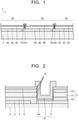
- FIG. 1 is a cross-sectional schematic view illustrating a structural example of the photoelectric conversion device.
- a photoelectric conversion device 1 illustrated in Fig. 1 has a substrate 2 functioning as a support substrate and a plurality of photoelectric conversion elements 3 (3A, 3B, 3C) disposed on the substrate 2.
- the photoelectric conversion elements 3 have substrate electrodes 4 (4A, 4B, 4C), photoelectric conversion layers 5 (5A, 5B, 5C), and counter electrodes 6 (6A, 6B, 6C) which are each provided on the substrate 2.
- the photoelectric conversion device 1 has connections 13 (13A, 13B) which have dividing grooves 11 (11A, 11B) exposing surfaces of the substrate electrodes and conductive layers 7 (7A, 7B) provided in the dividing grooves 11 and which electrically connects two photoelectric conversion elements 3.
- the mode is applicable in which a photoelectric conversion layer 5 is formed on an opaque substrate 2 and a substrate electrode 4 is formed thereon.
- the substrate 2 is constituted by a material having a light transmitting property and an insulating property.
- an inorganic material such as non-alkali glass, quartz glass, or sapphire, or an organic material such as polyethylene (PE), polyethylene terephthalate (PET), polyethylene naphthalate (PEN), polyimide, polyamide, polyamide-imide, or liquid crystal polymer.
- the substrate may be a rigid substrate made of an inorganic material or an organic material, for example, or may be a flexible substrate made of an organic material or an ultrathin inorganic material.
- the photoelectric conversion device 1 of the arrangement is a photovoltaic module
- light is irradiated to the photoelectric conversion layer 5 via the substrate 2 and the substrate electrode 4.
- the photoelectric conversion device 1 is a light emitting element
- the photoelectric conversion device 1 is the photovoltaic module
- the light irradiated to the photoelectric conversion layer 5 causes charge separation, which generates an electron and a hole to be a pair therewith.
- the electron is collected by the substrate electrode 4 and the hole is collected by the counter electrode 6, for example. Functions of the substrate electrode 4 and the counter electrode 6 may be reversed.
- those respective parts will be described.
- the substrate electrode 4 is constituted by a material having a light transmitting property and a conductivity, for example.
- a conductive metal oxide such as indium oxide, zinc oxide, tin oxide, indium tin oxide (ITO), fluorine-doped tin oxide (FTO), gallium-doped zinc oxide (GZO), aluminum-doped zinc oxide (AZO), indium-zinc oxide (IZO), or indium-gallium-zinc oxide (IGZO)
- a conductive polymer such as poly(3,4-ethylenedioxythiophene)/poly(4- styrenesulfonic acid) (PEDOT/PSS), or a carbon material such as graphene.
- the substrate electrode 4 may be a stacked film made of a layer constituted by the aforementioned material and a metal layer constituted by metal such as gold, platinum, silver, copper, cobalt, nickel, indium, or aluminum, or an alloy containing such metal, in a range where the light transmitting property can be maintained.
- the substrate electrode 4 is formed by a vacuum deposition method, a sputtering method, an ion plating method, a chemical vapor deposition (CVD) method, a sol-gel method, a plating method, a coating method, or the like, for example.
- a thickness of the substrate electrode 4 is not limited in particular, but is preferably 10 nm or more and 1 ⁇ m or less, and further preferably 30 nm or more and 300 nm or less.
- a sheet resistance becomes high.
- the film thickness of the substrate electrode 4 is too large, the light transmittance is reduced and flexibility is lowered, so that a crack is likely to occur by a stress.
- the sheet resistance of the substrate electrode 4 is not limited in particular, but is normally 1000 ⁇ / ⁇ or less, preferably 500 ⁇ / ⁇ or less, and more preferably 200 ⁇ / ⁇ or less. In a case of a current-driven type element such as a photovoltaic module or a light emitting element, the sheet resistance is further preferable to be 50 ⁇ / ⁇ or less.
- the photoelectric conversion layer 5 is disposed between a pair of opposing electrodes at least either one of which is the substrate electrode, and has a first intermediate layer (first buffer layer) disposed between the substrate electrode 4 and the photoelectric conversion layer 5, and a second intermediate layer (second buffer layer) disposed between the photoelectric conversion layer 5 and the counter electrode 6.
- the intermediate layer is disposed as necessary, and both or one of the respective intermediate layers is dispensable depending on the circumstances.
- Each layer constituting the element is appropriately selected in correspondence to a device (photovoltaic module, light emitting element, photosensor, or the like) to which the photoelectric conversion device is applied.
- a device photovoltaic module, light emitting element, photosensor, or the like
- the photoelectric conversion layer 5 has an active layer having a perovskite compound, for example.
- the perovskite compound is represented by a composition formula: ABX 3 , where A denotes at least one cation selected from the group consisting of monovalent cations, B denotes at least one cation selected from the group consisting of divalent cations, and X denotes at least one selected from the group consisting of halogen anions.
- A include at least one cation selected from the group consisting of methylammonium cation, formamidinium cation, potassium ion, rubidium ion, and cesium ion.
- Examples of B include at least one cation selected from the group consisting of lead ion, germanium ion, and tin ion.
- Examples of X include at least one halogen selected from the group consisting of iodine, bromine, and chlorine.
- the active layer having the perovskite compound is preferably formed by using a two-step method, for example.
- the two-step method is a method of forming a BX 2 compound layer as a first step and providing an AX compound on the BX 2 compound layer as a second step, to make them react and form an active layer containing a perovskite compound.
- the method is not limited to the above, and an active layer may be formed by using a method of vacuum depositing or a method of heating and drying an applied solution.
- the counter electrode 6 is constituted by a material having a conductivity, and under certain circumstances, having a light transmitting property.
- a constituent material of the counter electrode 6 there is used metal such as platinum, gold, silver, copper, nickel, cobalt, iron, manganese, tungsten, titanium, zirconium, tin, zinc, aluminum, indium, chromium, lithium, sodium, potassium, rubidium, cesium, calcium, magnesium, barium, samarium, or terbium, an alloy containing the above, a conductive metal oxide such as indium-zinc oxide (IZO), a conductive polymer such as PEDOT/PSS, or a carbon material such as graphene , for example.
- IZO indium-zinc oxide
- PEDOT/PSS PEDOT/PSS
- carbon material such as graphene
- the counter electrode 6 is formed by a vacuum deposition method, a sputtering method, an ion plating method, a sol-gel method, a plating method, a coating method, or the like, for example.
- a larger average thickness of the counter electrode 6 is more preferable, since the counter electrode 6 is preferable to be low in resistance in a case of a common photovoltaic module, but thinning of the counter electrode 6 enables an increase in light transmittance of the counter electrode 6, and thus the counter electrode 6 is required to be formed thin in a case of producing a transparent photovoltaic module.
- a thickness is preferably 50 nm or less, and further preferably 20 nm or less. The above is not necessarily applicable when a transparent electrode which originally has a high light transmitting property such as ITO is used as a counter electrode.
- the light transmittance of the counter electrode 6 is preferable to be 10% or more, for example. The light transmittance is measured by using an ultraviolet-visible spectrophotometer, for example.
- a sheet resistance of the counter electrode 6 is preferably 1000 ⁇ / ⁇ or less, and more preferably 50 ⁇ / ⁇ or less.
- Fig. 2 is a cross-sectional schematic view illustrating a structural example of the photoelectric conversion layer 5 and the connection 13.
- the photoelectric conversion layer 5 has an active layer 51, an intermediate layer 52 disposed between the substrate electrode 4 and the active layer 51, and an intermediate layer 53 disposed between the active layer 51 and the counter electrode 6.
- an active layer containing the above-described perovskite compound for example, can be used.
- a thickness of the active layer 51 is not limited in particular, but is preferably 10 nm or more and 1000 nm or less.
- the intermediate layer 52 and the intermediate layer 53 are disposed as necessary, and both or either one of them is dispensable depending on the circumstances.
- the intermediate layer 52 is constituted by a material capable of transporting the electron selectively and efficiently.
- a constituent material of the intermediate layer 52 functioning as an electron transport layer there can be cited an inorganic material such as zinc oxide, titanium oxide, or gallium oxide, an organic material such as polyethyleneimine or its derivative, and a carbon material such as the aforementioned fullerene derivative, but the constituent material is not limited in particular.
- the intermediate layer 52 is constituted by a material capable of transporting the hole selectively and efficiently.
- a constituent material of the intermediate layer 52 functioning as a hole transport layer there can be cited an inorganic material such as nickel oxide, copper oxide, vanadium oxide, tantalum oxide, or molybdenum oxide, and an organic material such as polythiophene, polypyrrole, polyacethylene, triphenylenediaminepolypyrrol, polyaniline, or a derivative of the above, but the constituent material is not limited in particular.
- the intermediate layer 53 is constituted by a material capable of transporting the hole selectively and efficiently.
- a constituent material of the intermediate layer 53 functioning as the hole transport layer is similar to the constituent material of the intermediate layer 52.
- the intermediate layer 53 is constituted by a material capable of transporting the electron selectively and efficiently.
- a constituent material of the intermediate layer 53 functioning as the electron transport layer is similar to the constituent material of the intermediate layer 52.
- the intermediate layer 52 and the intermediate layer 53 are formed by a vacuum deposition method, a sputtering method, an ion plating method, a CVD method, a sol-gel method, a plating method, a coating method, or the like, for example. Thicknesses are each preferably 1 nm or more and 200 nm or less.
- a lower resistance of the counter electrode 6 is more preferable, but thinning of the counter electrode 6 for the sake of lowering the resistance causes the following problem.
- a method of dividing the photoelectric conversion layer 5 there is used mechanical scribing by using a cutting tool, laser scribing by using laser, or the like, but in both methods, in first scribing to expose the substrate electrode 4 in order to expose the substrate electrode 4, a projection (burr 12) of a film may occur on an edge portion of the dividing groove 11, that is, in an end portion of the photoelectric conversion element 3 as illustrated in Fig. 2 , by an impact of scribing, so that flatness of an upper surface of the photoelectric conversion element 3 is sometimes impaired notably by the burr 12 of the end portion. Note that the burr 12 is not necessarily required to exist.
- the counter electrode 6 When the counter electrode 6 is formed by a vacuum process, electrical continuity is formed between the end portion of the photoelectric conversion element 3 and the substrate electrode 4 via the dividing groove 11 by the counter electrode 6 formed by the vacuum process. However, if the counter electrode 6 is thinned, by the burr 12 and a level difference between the upper surface of the photoelectric conversion element 3 and the substrate electrode 4, there may occur benching of a conductive portion, a reduction of the property as the photoelectric conversion device due to an electrical bottleneck caused by thinning of the counter electrode 6, or a reduction of a yield.
- connection 13 illustrated in Fig. 2 has the dividing groove 11, a conductive portion 6a made of a part of the counter electrode 6 provided in the dividing groove 11, and a conductive layer 7 provided in the dividing groove 11.
- the connection 13 electrically connects the counter electrode 6 of one of the photoelectric conversion elements 3 and the substrate electrode 4 of another photoelectric conversion element 3 by the conductive portion 6a and the conductive layer 7.
- the conductive layer 7 is provided on the conductive portion 6a, extends along an inner wall surface of the dividing groove 11, and overlaps one of the counter electrodes 6 in the edge of the dividing groove 11. Note that the conductive layer 7 may overlap an end portion adjacent to the photoelectric conversion layer 5 other than one of the photoelectric conversion layers 5.
- a material applicable to the counter electrode 6, for example, can be used for the conductive layer 7.
- a total thickness of the conductive portion 6a and the conductive layer 7 is preferably larger than the thickness of the counter electrode 6. Thereby, a connection resistance between the counter electrode 6 and the substrate electrode 4 in the connection 3 can be lowered.
- An average thickness of the conductive layer 7 is preferable to be 30 nm or more and 1000 nm or less, for example.
- a sheet resistance of the conductive layer 7 is preferably 1000 ⁇ / ⁇ or less and more preferably 50 ⁇ / ⁇ or less.
- a light transmittance of the conductive layer 7 may be less than 10%.
- the counter electrode 6 and the conductive layer 7 can be discriminated based on a difference in light transmittance.
- Fig. 3A to Fig. 3D are schematic views for explaining the manufacturing method example of the photoelectric conversion device 1.
- substrate electrodes 4A, 4B, 4C corresponding to a plurality of photoelectric conversion elements 3A, 3B, 3C are formed on the substrate 2.
- the substrate electrode 4B is formed in a state of being adjacent to the substrate electrode 4A and separate from the substrate electrode 4A, that is, in a state of being electrically insulated.
- the substrate electrode 4C is formed in a state of being adjacent to the substrate electrode 4B and separate from the substrate electrode 4B, that is, in a state of being electrically insulated.
- a photoelectric conversion layer 5X is formed on the substrate 2 in a manner to overlap the substrate electrodes 4A, 4B, 4C.
- the photoelectric conversion layer 5X is formed on an entire surface to overlap all the substrate electrodes 4A, 4B, 4C.
- the photoelectric conversion layer 5X is cut to form dividing grooves 11A, 11B so as to divide the photoelectric conversion layer 5X into a plurality of layers to correspond to the respective photoelectric conversion elements 3A, 3B, 3C.
- the dividing grooves 11A, 11B which divide the photoelectric conversion layer 5X are formed by a scribing method such as mechanical scribing or laser scribing, for example.
- the dividing grooves 11A, 11B are forming regions of the electrical connections 13A, 13B between the counter electrodes 6A, 6B of the photoelectric conversion elements 3A, 3B and the substrate electrodes 4B, 4C of the adjacent photoelectric conversion elements 3B, 3C. Therefore, the dividing grooves 11A, 11B are formed in a manner that surfaces of the substrate electrodes 4B, 4C are exposed.
- counter electrodes 6A, 6B, 6C corresponding to the plurality of photoelectric conversion elements 3A, 3B, 3C respectively are formed on the photoelectric conversion layers 5A, 5B, 5C.
- parts (conductive portions 6a) of the counter electrodes 6A, 6B are embedded in the dividing grooves 11A, 11B provided between the photoelectric conversion elements 3A, 3B and the adjacent photoelectric conversion elements 3B, 3C.
- the counter electrodes 6A, 6B of the photoelectric conversion elements 3A, 3B and the substrates electrodes 4B, 4C of the adjacent photoelectric conversion elements 3B, 3C are electrically connected by the conductive portions 6a filled in the dividing grooves 11A, 11B.
- parts of the intermediate layer 53 may be embedded in the dividing grooves 11A, 11B.
- Dividing of the counter electrodes 6A and 6B may be done by mask film-formation, and also may be done by using mechanical scribing or laser scribing after formation of a large film.
- conductive layers 7A, 7B are formed in the dividing grooves 11A, 11B provided between the photoelectric conversion elements 3A, 3B and the adjacent photoelectric conversion elements 3B, 3C.
- the counter electrodes 6A, 6B of the photoelectric conversion elements 3A, 3B and substrates electrodes 4B, 4C of the adjacent photoelectric conversion elements 3B, 3C are electrically connected by the conductive portions 6a filled in the dividing grooves 11A, 11B and the conductive layers 7A, 7B.
- parts of the intermediate layer 53 may be embedded in the dividing grooves 11A, 11B.
- Fig. 4 is a plan view for explaining the manufacturing method example of the photoelectric conversion device 1.
- the conductive layer 7A may be formed in a rectangular shape.
- a width of the conductive layer 7 is preferably larger than a width of the dividing groove 11, and preferably, for example, larger by 100 ⁇ m or more than the width of the dividing groove 11.
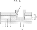
- Fig. 5 is a cross-sectional schematic view illustrating another structural example of the connection 13. Note that for parts similar to those in Fig. 1 and Fig. 2 , the above-described explanation can be appropriately used.
- a conductive portion 6a is not formed as illustrated in Fig. 5 , a conductive layer 7 whose thickness is larger than a thickness of a counter electrode 6 overlaps the counter electrode 6 on an edge of a dividing groove 11.
- the conductive layer 7 further contacts a substrate electrode 4 and the counter electrode 6. Thereby, the substrate electrode 4 and the counter electrode 6 are electrically connected.
- FIG. 6A to Fig. 6D are schematic views for explaining a manufacturing method example of a photoelectric conversion device 1. Note that for parts similar to those in the manufacturing method example of the photoelectric conversion device referring to Fig. 3 , the above-described explanation can be appropriately used.
- substrate electrodes 4A, 4B, 4C corresponding to a plurality of photoelectric conversion elements 3A, 3B, 3C are formed on a substrate 2.
- the substrate electrode 4B is formed in a state of being adjacent to the substrate electrode 4A and separate from the substrate electrode 4A, that is, in a state of being electrically insulated.
- the substrate electrode 4C is formed in a state of being adjacent to the substrate electrode 4B and separate from the substrate electrode 4B, that is, in a state of being electrically insulated.
- a photoelectric conversion layer 5X is formed on the substrate 2 in a manner to overlap the substrate electrodes 4A, 4B, 4C.
- the photoelectric conversion layer 5X is formed on an entire surface to overlap all the substrate electrodes 4A, 4B, 4C.
- a counter electrode 6X is formed on the photoelectric conversion layer 5X.
- a forming method of the counter electrode 6X is similar to that in the manufacturing method example of the photoelectric conversion device referring to Fig. 3 .
- the photoelectric conversion layer 5X and the counter electrode 6X are cut to form dividing grooves 11A, 11B so as to divide the photoelectric conversion layer 5X and the counter electrode 6X into a plurality of layers to correspond to the respective photoelectric conversion elements 3A, 3B, 3C.
- the dividing grooves 11A, 11B are formed by a scribing method such as mechanical scribing or laser scribing, for example.
- the photoelectric conversion layer 5X and the counter electrode 6X By dividing the photoelectric conversion layer 5X and the counter electrode 6X into the plurality of layers by the scribe grooves (dividing grooves) 11A, 11B, photoelectric conversion layers 5A, 5B, 5C and counter electrodes 6A, 6B, 6C corresponding to the plurality of photoelectric conversion elements 3A, 3B, 3C are formed.
- the dividing grooves 11A, 11B are forming regions of electrical connections 13 between the counter electrodes 6A, 6B of the photoelectric conversion elements 3A, 3B and the substrate electrodes 4B, 4C of the adjacent photoelectric conversion elements 3B, 3C. Therefore, the dividing grooves 11A, 11B are formed in a manner that surfaces of the substrate electrodes 4B, 4C are exposed.
- conductive layers 7A, 7B are formed in the dividing grooves 11A, 11B provided between the adjacent photoelectric conversion elements 3A, 3B, 3C.
- the counter electrodes 6A, 6B of the photoelectric conversion elements 3A, 3B and substrates electrodes 4B, 4C of the adjacent photoelectric conversion elements 3B, 3C are electrically connected by the conductive layers 7A, 7B provided in the dividing grooves 11A, 11B.
- a plurality of ITO layers of 150 nm in thickness were formed as substrate electrodes on a glass substrate. Eight ITO layers were formed in correspondence to the number of provided photoelectric conversion elements. In other words, the ITO layers were formed to correspond to an eight-series module.
- conductive layers having a stacked structure of Mo and Au were formed in edge portions on left sides of the eight ITO layers. The Mo layer was used as an adhesive layer between the ITO layer and the Au layer.
- a width of the conductive layer was about 0.5 mm, and a thickness thereof was 350 nm (Mo layer: 50 nm, Au layer: 300 nm).
- the conductive layer was formed by a vacuum film forming method and patterned by a photolithography method, to thereby be formed only in the edge portion of the ITO layer.
- PEDOT/PSS was formed as a substrate side intermediate layer.
- As the PEDOT ⁇ PSS Clevios A14083 of Heraeus Corporation was used. A film thickness was about 50 nm.
- a perovskite layer was formed as an active layer.
- a film forming method of the perovskite layer a two-step method was used.
- a coating solution for a first step there was used a solution in which Pbl 2 was dissolved in a 1 : 1 mixed solvent of dimethylformamide (DMF) and dimethylsulfoxide (DMSO).
- a coating solution for a second step there was used a solution in which CH 3 NH 3 I (MAI) was dissolved in isopropyl alcohol (IPA).
- IPA isopropyl alcohol
- a film was formed by vacuum depositing BCP (2,9-dimethyl-4,7-diphenyl-1,10-phenanthroline) in a thickness of about 20 nm.
- BCP 2,9-dimethyl-4,7-diphenyl-1,10-phenanthroline
- a film was formed by vacuum deposing Ag in a thickness of about 150 nm.
- Ag was further deposited in a thickness of 150 nm to thereby form a conductive layer in a manner that its size becomes larger than a width of the scribe groove by about 100 ⁇ m.
- a plurality of ITO layers of 150 nm in thickness were formed as substrate electrodes on a glass substrate. Eight ITO layers were formed in correspondence to the number of provided photoelectric conversion elements. In other words, the ITO layers were formed to correspond to an eight-series module.
- conductive layers having a stacked structure of Mo and Au were formed in edge portions on left sides of eight ITO layers. The Mo layer was used as an adhesive layer between the ITO layer and the Au layer.
- a width of the conductive layer was about 0.5 mm, and a thickness thereof was 350 nm (Mo layer: 50 nm, Au layer: 300 nm).
- the conductive layer was formed by a vacuum film forming method and patterned by a photolithography method, to thereby be formed only in the edge portion of the ITO layer.
- PEDOT/PSS was formed as a substrate side intermediate layer.
- As the PEDOT ⁇ PSS Clevios A14083 of Heraeus Corporation was used. A film thickness was about 50 nm.
- a perovskite layer was formed as an active layer.
- a film forming method of the perovskite layer a two-step method was used.
- a coating solution for a first step there was used a solution in which Pbl 2 was dissolved in a 1 : 1 mixed solvent of dimethylformamide (DMF) and dimethylsulfoxide (DMSO).
- a coating solution for a second step there was used a solution in which CH 3 NH 3 I (MAI) was dissolved in isopropyl alcohol (IPA).
- IPA isopropyl alcohol
- AZO was applied and formed, and thereafter ITO was formed by sputtering.
- a film was formed by vacuum depositing BCP in a thickness of about 20 nm.
- a film was formed by vacuum deposing Ag in a thickness of about 150 nm.
- Ag was further deposited in a thickness of 150 nm to thereby form a conductive layer in a manner that its size becomes larger than a width of the scribe groove by about 100 ⁇ m.
- Example 1 an ITO substrate electrode, a substrate side intermediate layer, CH 3 NH 3 PbI 3 (MAPbI 3 ), counter electrode side intermediate layers A, B were applied and formed on a glass substrate, scribing was performed to a photoelectric conversion layer in order to connect segments in series, a through hole was provided in the substrate electrode, and thereafter, ITO of 30 nm was formed by sputtering as a counter electrode, and the counter electrode and the substrate electrode were electrically connected via the through hole. Thereafter, to a scribed groove part, Ag was further deposited in a thickness of 150 nm to thereby form a conductive layer in a manner that its size becomes larger than a width of the scribe groove by about 100 ⁇ m. Thereafter, scribing was performed to the counter electrode and the photoelectric conversion layer, to thereby electrically separate cells. A photoelectric conversion module which is translucent in form and has an improved series resistance was realized.
Landscapes
- Engineering & Computer Science (AREA)
- Chemical & Material Sciences (AREA)
- Materials Engineering (AREA)
- Physics & Mathematics (AREA)
- Electromagnetism (AREA)
- Photovoltaic Devices (AREA)
- Life Sciences & Earth Sciences (AREA)
- Sustainable Development (AREA)
- Sustainable Energy (AREA)
Abstract
Description
- Arrangements of the present invention relate to a photoelectric conversion device and a method of manufacturing the photoelectric conversion device.
- For a perovskite photovoltaic module, an inexpensive coating method is applicable to formation of an active layer or the like of the photovoltaic module, and it is possible to substantially reduce a forming cost of the active layer or the like. In that respect, the perovskite photovoltaic module is expected as a next-generation photovoltaic module which is low in cost and harmless.
- A cell constituting a photovoltaic module has a structure in which a substrate electrode and a counter electrode sandwich an active layer. At present, since the substrate electrode at a practical level does not have a sufficient conductivity, an efficiency of retrieving a generated electric charge to the outside deteriorates as a cell area is increased. As a constituent material of the substrate, there is used a conductive metal oxide, a conductive polymer, a carbon material, or the like, or further, a material obtained by compounding a metal nanowire or the like with the above. Thus, it is general to form the photovoltaic module by aligning a plurality of strip-shaped cells and to connect the plurality of cells in series. The photovoltaic module having the plurality of cells is formed by a method described hereinafter, for example. Substrate electrodes of respective cells are formed on a substrate. A photoelectric conversion layer is applied and formed on an entire surface on the plurality of substrate electrodes. Parts of the photoelectric conversion layer are scribed so as to form groves to expose the substrate electrodes. Counter electrodes are formed in correspondence to the respective cells on the photoelectric conversion layer having the scribe grooves. On this occasion, by filling the counter electrode of the adjacent cell in the scribe groove, the counter electrode of the adjacent cell and the substrate electrode exposed in the scribe groove are electrically connected. The counter electrodes are formed in an electrically separated state per the module by usage of masked vapor deposition, for example, or are electrically separated per the module later by scribing, for example.
-
- Reference 1:
JPB 5715795 - Reference 2:
JPB 6030176 - A problem to be solved by the present invention is to provide a photoelectric conversion element in which adjacent photoelectric conversion parts are electrically separated, and a method manufacturing thereof.
- A photoelectric conversion device of an embodiment, includes: a substrate; a first photoelectric conversion element including a first substrate electrode provided on the substrate, a first photoelectric conversion layer disposed on the first substrate electrode, and a first counter electrode disposed on the first photoelectric conversion layer; a second photoelectric conversion element including a second substrate electrode provided adjacent to the first substrate electrode on the substrate and electrically insulated from the first substrate electrode, a second photoelectric conversion layer disposed on the second substrate electrode, and a second counter electrode disposed on the second photoelectric conversion layer; and a connection including a groove, a conductive portion and a conductive layer, the groove penetrating the second photoelectric conversion layer from a surface to expose a surface of the second substrate electrode from the second photoelectric conversion layer, the conductive portion being provided in the groove and including a part of the first counter electrode, the conductive layer being provided on the conductive portion, and the conductive portion and the conductive layer electrically connecting the first counter electrode and the second substrate electrode. The conductive layer overlaps the first counter electrode on an edge of the groove, and a total thickness of the conductive portion and the conductive layer is larger than a thickness of the first counter electrode.
-
-
Fig. 1 is a cross-sectional schematic view illustrating a structural example of a photoelectric conversion device; -
Fig. 2 is a cross-sectional schematic view illustrating a structural example of a photoelectric conversion layer and a connection: -
Figs. 3A to 3D are cross-sectional views for explaining a manufacturing method example of the photoelectric conversion device; -
Fig. 4 is a plan view for explaining the manufacturing method example of the photoelectric conversion device; -
Fig. 5 is a cross-sectional schematic view illustrating another structural example of the connection; and -
Figs. 6A to 6D are cross-sectional views for exampling another manufacturing method example of the photoelectric conversion device. - Hereinafter, photoelectric conversion devices of arrangements and manufacturing methods thereof will be described with reference to the drawings. Note that in each arrangement, the same reference numeral is given to practically the same component and explanation thereof may be partially omitted. The drawings are schematic and a relationship between a thickness and a plan dimension, a ratio of thicknesses of respective portions, and so on may be different from real ones. A term indicating a direction such as up/down in explanation indicates a relative direction in a case where a surface of a later-described substrate on which a photoelectric conversion element is formed is defined as up, unless clearly notified in particular, and may be different from a real direction based on a gravitational acceleration direction.
-
Fig. 1 is a cross-sectional schematic view illustrating a structural example of the photoelectric conversion device. Aphotoelectric conversion device 1 illustrated inFig. 1 has asubstrate 2 functioning as a support substrate and a plurality of photoelectric conversion elements 3 (3A, 3B, 3C) disposed on thesubstrate 2. The photoelectric conversion elements 3 have substrate electrodes 4 (4A, 4B, 4C), photoelectric conversion layers 5 (5A, 5B, 5C), and counter electrodes 6 (6A, 6B, 6C) which are each provided on thesubstrate 2. Further, thephotoelectric conversion device 1 has connections 13 (13A, 13B) which have dividing grooves 11 (11A, 11B) exposing surfaces of the substrate electrodes and conductive layers 7 (7A, 7B) provided in the dividinggrooves 11 and which electrically connects two photoelectric conversion elements 3. - In this arrangement there is described an example of a mode in which light incidence and emission is performed on a
substrate 2 side by using a transparent substrate as thesubstrate 2 and forming atransparent substrate electrode 4 on thesubstrate 2, but a reverse mode may be applied. That is, the mode is applicable in which aphotoelectric conversion layer 5 is formed on anopaque substrate 2 and asubstrate electrode 4 is formed thereon. - The
substrate 2 is constituted by a material having a light transmitting property and an insulating property. As a constituent material of thesubstrate 2, there is used an inorganic material such as non-alkali glass, quartz glass, or sapphire, or an organic material such as polyethylene (PE), polyethylene terephthalate (PET), polyethylene naphthalate (PEN), polyimide, polyamide, polyamide-imide, or liquid crystal polymer. The substrate may be a rigid substrate made of an inorganic material or an organic material, for example, or may be a flexible substrate made of an organic material or an ultrathin inorganic material. - In a case where the
photoelectric conversion device 1 of the arrangement is a photovoltaic module, light is irradiated to thephotoelectric conversion layer 5 via thesubstrate 2 and thesubstrate electrode 4. In a case where thephotoelectric conversion device 1 is a light emitting element, light generated by thephotoelectric conversion layer 5 is emitted via thesubstrate 2 and thesubstrate electrode 4. In the case where thephotoelectric conversion device 1 is the photovoltaic module, the light irradiated to thephotoelectric conversion layer 5 causes charge separation, which generates an electron and a hole to be a pair therewith. Of the electron and the hole generated by thephotoelectric conversion layer 5, the electron is collected by thesubstrate electrode 4 and the hole is collected by thecounter electrode 6, for example. Functions of thesubstrate electrode 4 and thecounter electrode 6 may be reversed. Hereinafter, those respective parts will be described. - The
substrate electrode 4 is constituted by a material having a light transmitting property and a conductivity, for example. As a constituent material of thesubstrate electrode 4, there is used a conductive metal oxide such as indium oxide, zinc oxide, tin oxide, indium tin oxide (ITO), fluorine-doped tin oxide (FTO), gallium-doped zinc oxide (GZO), aluminum-doped zinc oxide (AZO), indium-zinc oxide (IZO), or indium-gallium-zinc oxide (IGZO), a conductive polymer such as poly(3,4-ethylenedioxythiophene)/poly(4- styrenesulfonic acid) (PEDOT/PSS), or a carbon material such as graphene. It is possible to use a conductive nano-material such as a silver nanowire, a gold nanowire, or a carbon nanotube by mixing it in the aforementioned material. Further, thesubstrate electrode 4 may be a stacked film made of a layer constituted by the aforementioned material and a metal layer constituted by metal such as gold, platinum, silver, copper, cobalt, nickel, indium, or aluminum, or an alloy containing such metal, in a range where the light transmitting property can be maintained. Thesubstrate electrode 4 is formed by a vacuum deposition method, a sputtering method, an ion plating method, a chemical vapor deposition (CVD) method, a sol-gel method, a plating method, a coating method, or the like, for example. - A thickness of the
substrate electrode 4 is not limited in particular, but is preferably 10 nm or more and 1 µm or less, and further preferably 30 nm or more and 300 nm or less. When the film thickness of thesubstrate electrode 4 is too small, a sheet resistance becomes high. When the film thickness of thesubstrate electrode 4 is too large, the light transmittance is reduced and flexibility is lowered, so that a crack is likely to occur by a stress. For thesubstrate electrode 4, it is preferable to choose the film thickness so as to achieve both high light transmittance and low sheet resistance. The sheet resistance of thesubstrate electrode 4 is not limited in particular, but is normally 1000 Ω/□ or less, preferably 500 Ω/□ or less, and more preferably 200 Ω/□ or less. In a case of a current-driven type element such as a photovoltaic module or a light emitting element, the sheet resistance is further preferable to be 50 Ω/□ or less. - The
photoelectric conversion layer 5 is disposed between a pair of opposing electrodes at least either one of which is the substrate electrode, and has a first intermediate layer (first buffer layer) disposed between thesubstrate electrode 4 and thephotoelectric conversion layer 5, and a second intermediate layer (second buffer layer) disposed between thephotoelectric conversion layer 5 and thecounter electrode 6. The intermediate layer is disposed as necessary, and both or one of the respective intermediate layers is dispensable depending on the circumstances. Each layer constituting the element is appropriately selected in correspondence to a device (photovoltaic module, light emitting element, photosensor, or the like) to which the photoelectric conversion device is applied. Hereinafter, a case where the photoelectric conversion device is used as the photovoltaic module is mainly described, but the photoelectric conversion device of the arrangement can be applied to the light emitting element, the photosensor, or the like. - The
photoelectric conversion layer 5 has an active layer having a perovskite compound, for example. The perovskite compound is represented by a composition formula: ABX3, where A denotes at least one cation selected from the group consisting of monovalent cations, B denotes at least one cation selected from the group consisting of divalent cations, and X denotes at least one selected from the group consisting of halogen anions. Examples of A include at least one cation selected from the group consisting of methylammonium cation, formamidinium cation, potassium ion, rubidium ion, and cesium ion. Examples of B include at least one cation selected from the group consisting of lead ion, germanium ion, and tin ion. Examples of X include at least one halogen selected from the group consisting of iodine, bromine, and chlorine. - The active layer having the perovskite compound is preferably formed by using a two-step method, for example. The two-step method is a method of forming a BX2 compound layer as a first step and providing an AX compound on the BX2 compound layer as a second step, to make them react and form an active layer containing a perovskite compound. The method is not limited to the above, and an active layer may be formed by using a method of vacuum depositing or a method of heating and drying an applied solution.
- The
counter electrode 6 is constituted by a material having a conductivity, and under certain circumstances, having a light transmitting property. As a constituent material of thecounter electrode 6, there is used metal such as platinum, gold, silver, copper, nickel, cobalt, iron, manganese, tungsten, titanium, zirconium, tin, zinc, aluminum, indium, chromium, lithium, sodium, potassium, rubidium, cesium, calcium, magnesium, barium, samarium, or terbium, an alloy containing the above, a conductive metal oxide such as indium-zinc oxide (IZO), a conductive polymer such as PEDOT/PSS, or a carbon material such as graphene , for example. It is possible to use a conductive nano-material such as a silver nanowire, a gold nanowire, or a carbon nanotube by mixing it in the aforementioned material. Thecounter electrode 6 is formed by a vacuum deposition method, a sputtering method, an ion plating method, a sol-gel method, a plating method, a coating method, or the like, for example. - A larger average thickness of the
counter electrode 6 is more preferable, since thecounter electrode 6 is preferable to be low in resistance in a case of a common photovoltaic module, but thinning of thecounter electrode 6 enables an increase in light transmittance of thecounter electrode 6, and thus thecounter electrode 6 is required to be formed thin in a case of producing a transparent photovoltaic module. For example, when a silver electrode is used as a counter electrode, a thickness is preferably 50 nm or less, and further preferably 20 nm or less. The above is not necessarily applicable when a transparent electrode which originally has a high light transmitting property such as ITO is used as a counter electrode. The light transmittance of thecounter electrode 6 is preferable to be 10% or more, for example. The light transmittance is measured by using an ultraviolet-visible spectrophotometer, for example. - A sheet resistance of the
counter electrode 6 is preferably 1000 Ω/□ or less, and more preferably 50 Ω/□ or less. -
Fig. 2 is a cross-sectional schematic view illustrating a structural example of thephotoelectric conversion layer 5 and theconnection 13. Thephotoelectric conversion layer 5 has anactive layer 51, anintermediate layer 52 disposed between thesubstrate electrode 4 and theactive layer 51, and anintermediate layer 53 disposed between theactive layer 51 and thecounter electrode 6. - As the
active layer 51, an active layer containing the above-described perovskite compound, for example, can be used. A thickness of theactive layer 51 is not limited in particular, but is preferably 10 nm or more and 1000 nm or less. Theintermediate layer 52 and theintermediate layer 53 are disposed as necessary, and both or either one of them is dispensable depending on the circumstances. - In a case where the electron is collected by the
substrate electrode 4, of the electron and the hole generated by thephotoelectric conversion layer 5, theintermediate layer 52 is constituted by a material capable of transporting the electron selectively and efficiently. As a constituent material of theintermediate layer 52 functioning as an electron transport layer, there can be cited an inorganic material such as zinc oxide, titanium oxide, or gallium oxide, an organic material such as polyethyleneimine or its derivative, and a carbon material such as the aforementioned fullerene derivative, but the constituent material is not limited in particular. - In a case where the hole is collected by the
substrate electrode 4, theintermediate layer 52 is constituted by a material capable of transporting the hole selectively and efficiently. As a constituent material of theintermediate layer 52 functioning as a hole transport layer, there can be cited an inorganic material such as nickel oxide, copper oxide, vanadium oxide, tantalum oxide, or molybdenum oxide, and an organic material such as polythiophene, polypyrrole, polyacethylene, triphenylenediaminepolypyrrol, polyaniline, or a derivative of the above, but the constituent material is not limited in particular. - In a case where the hole is collected by the
counter electrode 6, of the electron and the hole generated by thephotoelectric conversion layer 5, theintermediate layer 53 is constituted by a material capable of transporting the hole selectively and efficiently. A constituent material of theintermediate layer 53 functioning as the hole transport layer is similar to the constituent material of theintermediate layer 52. In a case where the electron is collected by thecounter electrode 6, theintermediate layer 53 is constituted by a material capable of transporting the electron selectively and efficiently. A constituent material of theintermediate layer 53 functioning as the electron transport layer is similar to the constituent material of theintermediate layer 52. - The
intermediate layer 52 and theintermediate layer 53 are formed by a vacuum deposition method, a sputtering method, an ion plating method, a CVD method, a sol-gel method, a plating method, a coating method, or the like, for example. Thicknesses are each preferably 1 nm or more and 200 nm or less. - In view of a performance of the photoelectric conversion device, a lower resistance of the
counter electrode 6 is more preferable, but thinning of thecounter electrode 6 for the sake of lowering the resistance causes the following problem. As a method of dividing thephotoelectric conversion layer 5, there is used mechanical scribing by using a cutting tool, laser scribing by using laser, or the like, but in both methods, in first scribing to expose thesubstrate electrode 4 in order to expose thesubstrate electrode 4, a projection (burr 12) of a film may occur on an edge portion of the dividinggroove 11, that is, in an end portion of the photoelectric conversion element 3 as illustrated inFig. 2 , by an impact of scribing, so that flatness of an upper surface of the photoelectric conversion element 3 is sometimes impaired notably by theburr 12 of the end portion. Note that theburr 12 is not necessarily required to exist. - When the
counter electrode 6 is formed by a vacuum process, electrical continuity is formed between the end portion of the photoelectric conversion element 3 and thesubstrate electrode 4 via the dividinggroove 11 by thecounter electrode 6 formed by the vacuum process. However, if thecounter electrode 6 is thinned, by theburr 12 and a level difference between the upper surface of the photoelectric conversion element 3 and thesubstrate electrode 4, there may occur benching of a conductive portion, a reduction of the property as the photoelectric conversion device due to an electrical bottleneck caused by thinning of thecounter electrode 6, or a reduction of a yield. - In a general photoelectric conversion device, since a
counter electrode 6 having sufficient thickness and electric conductivity is formed, electrical connection between thecounter electrode 6 and asubstrate electrode 4 is not impaired even if aburr 12 is formed on an edge of a dividinggroove 11, but when a thin-film metal electrode or the like is used as thecounter electrode 6, for example, for the sake of forming a photoelectric conversion device with a high light transmittance, existence of aburr 12 cannot be ignored in order to secure electrical connection between thecounter electrode 6 and thesubstrate electrode 4. As described above, it is necessary to suppress a connection resistance between thecounter electrode 6 and thesubstrate electrode 4 from becoming high due to making thecounter electrode 6 thinner or lower in resistance. - In contrast, the
connection 13 illustrated inFig. 2 has the dividinggroove 11, aconductive portion 6a made of a part of thecounter electrode 6 provided in the dividinggroove 11, and aconductive layer 7 provided in the dividinggroove 11. Theconnection 13 electrically connects thecounter electrode 6 of one of the photoelectric conversion elements 3 and thesubstrate electrode 4 of another photoelectric conversion element 3 by theconductive portion 6a and theconductive layer 7. - The
conductive layer 7 is provided on theconductive portion 6a, extends along an inner wall surface of the dividinggroove 11, and overlaps one of thecounter electrodes 6 in the edge of the dividinggroove 11. Note that theconductive layer 7 may overlap an end portion adjacent to thephotoelectric conversion layer 5 other than one of the photoelectric conversion layers 5. - For the
conductive layer 7, a material applicable to thecounter electrode 6, for example, can be used. A total thickness of theconductive portion 6a and theconductive layer 7 is preferably larger than the thickness of thecounter electrode 6. Thereby, a connection resistance between thecounter electrode 6 and thesubstrate electrode 4 in the connection 3 can be lowered. An average thickness of theconductive layer 7 is preferable to be 30 nm or more and 1000 nm or less, for example. - A sheet resistance of the
conductive layer 7 is preferably 1000 Ω/□ or less and more preferably 50 Ω/□ or less. A light transmittance of theconductive layer 7 may be less than 10%. For example, by forming thecounter electrode 6 having a light transmittance of 10% or more and theconductive layer 7 having a light transmittance of less than 10%, thecounter electrode 6 and theconductive layer 7 can be discriminated based on a difference in light transmittance. - Next, a manufacturing method example of the
photoelectric conversion device 1 will be described as a manufacturing method example of the photoelectric conversion device of the arrangement.Fig. 3A to Fig. 3D are schematic views for explaining the manufacturing method example of thephotoelectric conversion device 1. In the manufacturing method example of thephotoelectric conversion device 1, as illustrated inFig. 3A ,substrate electrodes photoelectric conversion elements substrate 2. Thesubstrate electrode 4B is formed in a state of being adjacent to thesubstrate electrode 4A and separate from thesubstrate electrode 4A, that is, in a state of being electrically insulated. Similarly, thesubstrate electrode 4C is formed in a state of being adjacent to thesubstrate electrode 4B and separate from thesubstrate electrode 4B, that is, in a state of being electrically insulated. Aphotoelectric conversion layer 5X is formed on thesubstrate 2 in a manner to overlap thesubstrate electrodes photoelectric conversion layer 5X is formed on an entire surface to overlap all thesubstrate electrodes - Next, as illustrated in
Fig. 3B , thephotoelectric conversion layer 5X is cut to form dividinggrooves photoelectric conversion layer 5X into a plurality of layers to correspond to the respectivephotoelectric conversion elements grooves photoelectric conversion layer 5X are formed by a scribing method such as mechanical scribing or laser scribing, for example. By dividing thephotoelectric conversion layer 5X into the plurality of layers by the scribe grooves (dividing grooves) 11A, 11B, photoelectric conversion layers 5A, 5B, 5C corresponding to the plurality ofphotoelectric conversion elements grooves counter electrodes photoelectric conversion elements substrate electrodes photoelectric conversion elements grooves substrate electrodes - Next, as illustrated in
Fig. 3C ,counter electrodes photoelectric conversion elements counter electrodes photoelectric conversion elements conductive portions 6a) of thecounter electrodes grooves photoelectric conversion elements photoelectric conversion elements counter electrodes photoelectric conversion elements substrates electrodes photoelectric conversion elements conductive portions 6a filled in the dividinggrooves intermediate layer 53 may be embedded in the dividinggrooves counter electrodes - Next, as illustrated in
Fig. 3D ,conductive layers 7A, 7B are formed in the dividinggrooves photoelectric conversion elements photoelectric conversion elements counter electrodes photoelectric conversion elements substrates electrodes photoelectric conversion elements conductive portions 6a filled in the dividinggrooves conductive layers 7A, 7B. Note that parts of theintermediate layer 53 may be embedded in the dividinggrooves -
Fig. 4 is a plan view for explaining the manufacturing method example of thephotoelectric conversion device 1. As illustrated inFig. 4 , theconductive layer 7A may be formed in a rectangular shape. A width of theconductive layer 7 is preferably larger than a width of the dividinggroove 11, and preferably, for example, larger by 100 µm or more than the width of the dividinggroove 11. - The
conducive parts 6a are not necessarily required to be formed in the dividinggrooves Fig. 5 is a cross-sectional schematic view illustrating another structural example of theconnection 13. Note that for parts similar to those inFig. 1 and Fig. 2 , the above-described explanation can be appropriately used. When aconductive portion 6a is not formed as illustrated inFig. 5 , aconductive layer 7 whose thickness is larger than a thickness of acounter electrode 6 overlaps thecounter electrode 6 on an edge of a dividinggroove 11. Theconductive layer 7 further contacts asubstrate electrode 4 and thecounter electrode 6. Thereby, thesubstrate electrode 4 and thecounter electrode 6 are electrically connected. - Another manufacturing method example of a photoelectric conversion device having the
connection 13 illustrated inFig. 5 will be described.Fig. 6A to Fig. 6D are schematic views for explaining a manufacturing method example of aphotoelectric conversion device 1. Note that for parts similar to those in the manufacturing method example of the photoelectric conversion device referring toFig. 3 , the above-described explanation can be appropriately used. - In another manufacturing method example of the
photoelectric conversion device 1, as illustrated inFig. 6A ,substrate electrodes photoelectric conversion elements substrate 2. Thesubstrate electrode 4B is formed in a state of being adjacent to thesubstrate electrode 4A and separate from thesubstrate electrode 4A, that is, in a state of being electrically insulated. Similarly, thesubstrate electrode 4C is formed in a state of being adjacent to thesubstrate electrode 4B and separate from thesubstrate electrode 4B, that is, in a state of being electrically insulated. Aphotoelectric conversion layer 5X is formed on thesubstrate 2 in a manner to overlap thesubstrate electrodes photoelectric conversion layer 5X is formed on an entire surface to overlap all thesubstrate electrodes - Next, as illustrated in
Fig. 6B , acounter electrode 6X is formed on thephotoelectric conversion layer 5X. A forming method of thecounter electrode 6X is similar to that in the manufacturing method example of the photoelectric conversion device referring toFig. 3 . - Next, as illustrated in
Fig. 6C , thephotoelectric conversion layer 5X and thecounter electrode 6X are cut to form dividinggrooves photoelectric conversion layer 5X and thecounter electrode 6X into a plurality of layers to correspond to the respectivephotoelectric conversion elements grooves photoelectric conversion layer 5X and thecounter electrode 6X into the plurality of layers by the scribe grooves (dividing grooves) 11A, 11B, photoelectric conversion layers 5A, 5B, 5C andcounter electrodes photoelectric conversion elements grooves electrical connections 13 between thecounter electrodes photoelectric conversion elements substrate electrodes photoelectric conversion elements grooves substrate electrodes - Next, as illustrated in
Fig. 6D ,conductive layers 7A, 7B are formed in the dividinggrooves photoelectric conversion elements counter electrodes photoelectric conversion elements substrates electrodes photoelectric conversion elements conductive layers 7A, 7B provided in the dividinggrooves - As described above, it is possible to form a structure in which the
conductive layers 7A, 7B overlap thecounter electrodes 6 in edges of the dividinggrooves 11 without forming theconductive portions 6a. Thereby, it is possible to lower a connection resistance between thecounter electrode 6 and thesubstrate electrode 4 in theconnection 13. - A plurality of ITO layers of 150 nm in thickness were formed as substrate electrodes on a glass substrate. Eight ITO layers were formed in correspondence to the number of provided photoelectric conversion elements. In other words, the ITO layers were formed to correspond to an eight-series module. Next, conductive layers having a stacked structure of Mo and Au were formed in edge portions on left sides of the eight ITO layers. The Mo layer was used as an adhesive layer between the ITO layer and the Au layer. A width of the conductive layer was about 0.5 mm, and a thickness thereof was 350 nm (Mo layer: 50 nm, Au layer: 300 nm). The conductive layer was formed by a vacuum film forming method and patterned by a photolithography method, to thereby be formed only in the edge portion of the ITO layer. Next, PEDOT/PSS was formed as a substrate side intermediate layer. As the PEDOT·PSS, Clevios A14083 of Heraeus Corporation was used. A film thickness was about 50 nm.
- Next, a perovskite layer was formed as an active layer. As a film forming method of the perovskite layer, a two-step method was used. As a coating solution for a first step, there was used a solution in which Pbl2 was dissolved in a 1 : 1 mixed solvent of dimethylformamide (DMF) and dimethylsulfoxide (DMSO). As a coating solution for a second step, there was used a solution in which CH3NH3I (MAI) was dissolved in isopropyl alcohol (IPA). After the second step was finished, a heat treatment at 120°C was performed for 5 minutes to form the active layer. A film thickness was about 350 nm.
- Next, as a counter electrode side intermediate layer A, [0049]PCBM([6,6]-phenyl-C61-butyric acid methyl ester) was formed. As a solvent for [0050]PCBM ink, monochlorobenzene was used. After the [0051]PCBM ink was applied, spontaneous drying was done. A film thickness was about 50 nm.
- Next, in order to connect segments in series, scribing was performed to a photoelectric conversion layer to thereby provide a through hole on the substrate electrode.
- Next, as a counter electrode side intermediate layer B, a film was formed by vacuum depositing BCP (2,9-dimethyl-4,7-diphenyl-1,10-phenanthroline) in a thickness of about 20 nm. Next, as a counter electrode, a film was formed by vacuum deposing Ag in a thickness of about 150 nm.
- Thereafter, to a scribed groove part, Ag was further deposited in a thickness of 150 nm to thereby form a conductive layer in a manner that its size becomes larger than a width of the scribe groove by about 100 µm.
- Thereafter, scribing was performed to the counter electrode and the photoelectric conversion layer, to thereby separate cells. By the above steps, a photoelectric conversion module having a serial structure was formed. Consequently, a fill factor (FF) of an IV property was improved, alteration of a contact part at a time of an endurance test was also decreased, and a rise of a series resistance Rs was also able to be suppressed.
- A plurality of ITO layers of 150 nm in thickness were formed as substrate electrodes on a glass substrate. Eight ITO layers were formed in correspondence to the number of provided photoelectric conversion elements. In other words, the ITO layers were formed to correspond to an eight-series module. Next, conductive layers having a stacked structure of Mo and Au were formed in edge portions on left sides of eight ITO layers. The Mo layer was used as an adhesive layer between the ITO layer and the Au layer. A width of the conductive layer was about 0.5 mm, and a thickness thereof was 350 nm (Mo layer: 50 nm, Au layer: 300 nm). The conductive layer was formed by a vacuum film forming method and patterned by a photolithography method, to thereby be formed only in the edge portion of the ITO layer. Next, PEDOT/PSS was formed as a substrate side intermediate layer. As the PEDOT·PSS, Clevios A14083 of Heraeus Corporation was used. A film thickness was about 50 nm.
- Next, a perovskite layer was formed as an active layer. As a film forming method of the perovskite layer, a two-step method was used. As a coating solution for a first step, there was used a solution in which Pbl2 was dissolved in a 1 : 1 mixed solvent of dimethylformamide (DMF) and dimethylsulfoxide (DMSO). As a coating solution for a second step, there was used a solution in which CH3NH3I (MAI) was dissolved in isopropyl alcohol (IPA). After the second step was finished, a heat treatment at 120°C was performed for 5 minutes to form the active layer. A film thickness was about 350 nm.
- Next, as a counter electrode side intermediate layer A, AZO was applied and formed, and thereafter ITO was formed by sputtering.
- Next, in order to connect segments in series, scribing was performed to a photoelectric conversion layer to thereby provide a through hole on the substrate electrode.
- Next, as a counter electrode side intermediate layer B, a film was formed by vacuum depositing BCP in a thickness of about 20 nm. Next, as a counter electrode, a film was formed by vacuum deposing Ag in a thickness of about 150 nm.
- Thereafter, to a scribed groove part, Ag was further deposited in a thickness of 150 nm to thereby form a conductive layer in a manner that its size becomes larger than a width of the scribe groove by about 100 µm.
- Thereafter, scribing was performed to the counter electrode and the photoelectric conversion layer, to thereby separate cells. By the above steps, a photovoltaic module module having a serial structure was formed. Consequently, a FF of an IV property was improved, alteration of a contact part at a time of an endurance test was also decreased, and a rise of a series resistance Rs was also able to be suppressed.
- Similarly to Example 1, an ITO substrate electrode, a substrate side intermediate layer, CH3NH3PbI3(MAPbI3), counter electrode side intermediate layers A, B were applied and formed on a glass substrate, scribing was performed to a photoelectric conversion layer in order to connect segments in series, a through hole was provided in the substrate electrode, and thereafter, ITO of 30 nm was formed by sputtering as a counter electrode, and the counter electrode and the substrate electrode were electrically connected via the through hole. Thereafter, to a scribed groove part, Ag was further deposited in a thickness of 150 nm to thereby form a conductive layer in a manner that its size becomes larger than a width of the scribe groove by about 100 µm. Thereafter, scribing was performed to the counter electrode and the photoelectric conversion layer, to thereby electrically separate cells. A photoelectric conversion module which is translucent in form and has an improved series resistance was realized.
- Several arrangements of the present invention have been explained, but these arrangements have been presented by way of example only, and are not intended to limit the scope of the invention. Those arrangements can be embodied in a variety of other forms, and various omissions, substitutions and changes may be made without departing from the spirit of the invention. These arrangements and their modifications are included in the scope and gist of the invention and are included in the invention described in claims and their equivalents.
Claims (9)
- A photoelectric conversion device, comprising:a substrate;a first photoelectric conversion element includinga first substrate electrode provided on the substrate,a first photoelectric conversion layer disposed on the first substrate electrode, anda first counter electrode disposed on the first photoelectric conversion layer;a second photoelectric conversion element includinga second substrate electrode provided adjacent to the first substrate electrode on the substrate and electrically insulated from the first substrate electrode,a second photoelectric conversion layer disposed on the second substrate electrode, anda second counter electrode disposed on the second photoelectric conversion layer; anda connection including a groove, a conductive portion and a conductive layer, the groove penetrating the second photoelectric conversion layer from a surface to expose a surface of the second substrate electrode from the second photoelectric conversion layer, the conductive portion being provided in the groove and including a part of the first counter electrode, the conductive layer being provided on the conductive portion, and the conductive portion and the conductive layer electrically connecting the first counter electrode and the second substrate electrode, whereinthe conductive layer overlaps the first counter electrode on an edge of the groove, and a total thickness of the conductive portion and the conductive layer is larger than a thickness of the first counter electrode.
- The device according to claim 1, wherein
the first counter electrode has a light transmittance of 10% or more. - The device according to claim 1, wherein
the second substrate electrode contains at least one conductive metal oxide selected from the group consisting of indium oxide, zinc oxide, tin oxide, indium tin oxide, fluorine-doped tin oxide, gallium-doped zinc oxide, aluminum-doped zinc oxide, indium-zinc oxide, and an indium-gallium-zinc oxide. - The device according to claim 1, wherein
an average thickness of the conductive layer is 30 nm or more and 1000 nm or less. - The device according to claim 1, wherein
a width of the conductive layer is larger than a width of the groove. - The device according to claim 1, wherein
the photoelectric conversion layer has a perovskite compound represented by a composition formula: ABX3, where A denotes at least one cation selected from the group consisting of monovalent cations, B denotes at least one cation selected from the group consisting of divalent cations, and X denotes at least one selected from the group consisting of halogen anions. - A photoelectric conversion device comprising:a substrate;a first photoelectric conversion element includinga first substrate electrode provided on the substrate,a first photoelectric conversion layer disposed on the first substrate electrode, anda first counter electrode disposed on the first photoelectric conversion layer;a second photoelectric conversion element includinga second substrate electrode provided adjacent to the first substrate electrode on the substrate and electrically insulated from the first substrate electrode,a second photoelectric conversion layer disposed on the second substrate electrode, anda second counter electrode disposed on the second photoelectric conversion layer; anda connection including a groove and a conductive layer, the groove penetrating the second photoelectric conversion layer from a surface to expose a surface of the second substrate electrode from the second photoelectric conversion layer, the conductive layer being provided in the groove and electrically connecting the first counter electrode and the second substrate electrode, whereinthe conductive layer overlaps the first counter electrode on an edge of the groove and is thicker than the first counter electrode.
- A method of manufacturing a photoelectric conversion device, comprising:forming a first and a second substrate electrode onto a substrate, the second substrate electrode being adjacent to the first substrate electrode and electrically insulated from the first substrate electrode;forming a photoelectric conversion layer onto the substrate to overlap the first substrate electrode and the second substrate electrode;scribing the photoelectric conversion layer to form a groove penetrating the photoelectric conversion layer from a surface to expose a surface of the second substrate electrode from the photoelectric conversion layer;forming a first and a second counter electrode respectively corresponding to the first and the second substrate electrode onto the photoelectric conversion layer divided by the groove while forming a conductive portion including a part of the first counter electrode into the groove; andforming a conductive layer onto the conductive portion, the conductive layer overlapping the first counter electrode on an edge of the groove, a total thickness of the conductive portion and the conductive layer being larger than a thickness of the first counter electrode, the conductive portion and the conductive layer electrically connecting the first counter electrode and the second substrate electrode.
- A method of manufacturing a photoelectric conversion device, comprising:forming a first and a second substrate electrode onto a substrate, the second substrate electrode being adjacent to the first substrate electrode and electrically insulated from the first substrate electrode;forming a photoelectric conversion layer onto the substrate and overlap the first and second substrate electrodes;forming a counter electrode onto the photoelectric conversion layer;scribing the photoelectric conversion layer and the counter electrode to form a groove penetrating the photoelectric conversion layer from a surface to expose a surface of the second substrate electrode from the photoelectric conversion layer, while to form a first counter electrode and a second counter electrode in correspondence to the first substrate electrode and the second substrate electrode; andforming a conductive layer into the groove, the conductive layer being thicker than the first counter electrode, the conductive layer overlapping the first counter electrode on an edge of the groove, the conductive layer electrically connecting the first counter electrode and the second substrate electrode.
Applications Claiming Priority (1)
| Application Number | Priority Date | Filing Date | Title |
|---|---|---|---|
| PCT/JP2019/011596 WO2020188777A1 (en) | 2019-03-19 | 2019-03-19 | Photoelectric conversion element and method for manufacturing photoelectric conversion element |
Publications (2)
| Publication Number | Publication Date |
|---|---|
| EP3944350A1 true EP3944350A1 (en) | 2022-01-26 |
| EP3944350A4 EP3944350A4 (en) | 2022-10-12 |
Family
ID=72519754
Family Applications (1)
| Application Number | Title | Priority Date | Filing Date |
|---|---|---|---|
| EP19916574.7A Pending EP3944350A4 (en) | 2019-03-19 | 2019-03-19 | PHOTOELECTRIC CONVERSION ELEMENT AND METHOD OF MAKING PHOTOELECTRIC CONVERSION ELEMENT |
Country Status (4)
| Country | Link |
|---|---|
| US (1) | US11489081B2 (en) |
| EP (1) | EP3944350A4 (en) |
| JP (1) | JP7186785B2 (en) |
| WO (1) | WO2020188777A1 (en) |
Families Citing this family (4)
| Publication number | Priority date | Publication date | Assignee | Title |
|---|---|---|---|---|
| CN111180532B (en) * | 2020-01-06 | 2022-06-10 | 武汉华星光电技术有限公司 | A photodiode and its manufacturing method and display screen |
| JP7827054B2 (en) | 2021-02-24 | 2026-03-10 | 日本ゼオン株式会社 | Photoelectric conversion module and manufacturing method thereof |
| JP7801340B2 (en) * | 2022-01-24 | 2026-01-16 | 香港時代新能源科技有限公司 | Solar cell and method of manufacturing the same, photovoltaic assembly and power consumption device |
| TWI808759B (en) | 2022-05-13 | 2023-07-11 | 天光材料科技股份有限公司 | Electrode connection structure and method of forming the same |
Family Cites Families (24)
| Publication number | Priority date | Publication date | Assignee | Title |
|---|---|---|---|---|
| JPS5397003A (en) | 1977-02-04 | 1978-08-24 | Chiyoda Chem Eng & Constr Co Ltd | Thermal cracking treatment of petroleum heavy oil |
| JPS6030176B2 (en) | 1977-09-20 | 1985-07-15 | 日立電線株式会社 | overhead power transmission and distribution lines |
| JPH02100375A (en) * | 1988-10-07 | 1990-04-12 | Mitsubishi Electric Corp | Manufacture of photoelectric converting device |
| JP3017422B2 (en) | 1995-09-11 | 2000-03-06 | キヤノン株式会社 | Photovoltaic element array and manufacturing method thereof |
| JP5081389B2 (en) * | 2006-02-23 | 2012-11-28 | 三洋電機株式会社 | Method for manufacturing photovoltaic device |
| TW201037845A (en) * | 2009-04-10 | 2010-10-16 | Ritdisplay Corp | Photovoltaic cell structure and manufacturing method |
| WO2011052584A1 (en) | 2009-10-29 | 2011-05-05 | 住友化学株式会社 | Method for manufacturing organic thin-film solar battery module |
| JP2011135027A (en) * | 2009-11-26 | 2011-07-07 | Kyocera Corp | Photoelectric conversion device |
| JP5440439B2 (en) * | 2010-08-05 | 2014-03-12 | 三菱電機株式会社 | Method for manufacturing thin film photoelectric conversion device |
| KR101173418B1 (en) * | 2011-07-29 | 2012-08-10 | 엘지이노텍 주식회사 | Solar cell and method of fabricating the same |
| NL2014041B1 (en) * | 2014-12-23 | 2016-10-12 | Stichting Energieonderzoek Centrum Nederland | Method for manufacturing a thin film solar cell arrangement and such a thin film solar cell arrangement. |
| JP6030176B2 (en) | 2015-03-19 | 2016-11-24 | 株式会社東芝 | Photoelectric conversion element and manufacturing method thereof |
| EP3419067A4 (en) * | 2016-02-18 | 2019-10-02 | Sekisui Chemical Co., Ltd. | SOLID JUNCTION PHOTOELECTRIC CONVERSION ELEMENT MODULE AND METHOD FOR MANUFACTURING THE SAME |
| WO2017159192A1 (en) | 2016-03-18 | 2017-09-21 | コニカミノルタ株式会社 | Photoelectric conversion element and optical sensor |
| WO2017190787A1 (en) * | 2016-05-04 | 2017-11-09 | Bayerisches Zentrum Für Angewandte Energieforschung E. V. (Zae Bayern) | Method for fabricating a solar module, sub-laminate for fabricating a solar module and solar module |
| EP3509118A4 (en) * | 2016-08-31 | 2020-04-22 | KYOCERA Corporation | SOLAR CELL AND MANUFACTURING METHOD OF SOLAR CELL |
| JP6530360B2 (en) | 2016-09-23 | 2019-06-12 | 株式会社東芝 | Photoelectric conversion element |
| JP2018056213A (en) * | 2016-09-26 | 2018-04-05 | 積水化学工業株式会社 | Flexible solar cell and method for manufacturing flexible solar cell |
| JP6408042B2 (en) | 2017-01-24 | 2018-10-17 | 株式会社東芝 | Photoelectric conversion element and manufacturing method thereof |
| TWI636602B (en) * | 2017-03-21 | 2018-09-21 | 機光科技股份有限公司 | Organic optoelectronic device structure and manufacturing method |
| JP6487005B1 (en) | 2017-09-14 | 2019-03-20 | 株式会社東芝 | Photoelectric conversion element and manufacturing method thereof |
| JP6600670B2 (en) | 2017-09-15 | 2019-10-30 | 株式会社東芝 | Photoelectric conversion element, manufacturing method thereof, and manufacturing apparatus thereof |
| JPWO2019054240A1 (en) * | 2017-09-15 | 2020-10-15 | 出光興産株式会社 | How to manufacture photoelectric conversion module and photoelectric conversion module |
| US11329177B2 (en) * | 2018-11-08 | 2022-05-10 | Swift Solar Inc | Stable perovskite module interconnects |
-
2019
- 2019-03-19 JP JP2020542359A patent/JP7186785B2/en active Active
- 2019-03-19 EP EP19916574.7A patent/EP3944350A4/en active Pending
- 2019-03-19 WO PCT/JP2019/011596 patent/WO2020188777A1/en not_active Ceased
-
2020
- 2020-09-04 US US17/013,248 patent/US11489081B2/en active Active
Also Published As
| Publication number | Publication date |
|---|---|
| EP3944350A4 (en) | 2022-10-12 |
| WO2020188777A1 (en) | 2020-09-24 |
| US11489081B2 (en) | 2022-11-01 |
| JPWO2020188777A1 (en) | 2021-04-01 |
| US20200403108A1 (en) | 2020-12-24 |
| JP7186785B2 (en) | 2022-12-09 |
Similar Documents
| Publication | Publication Date | Title |
|---|---|---|
| US10305055B2 (en) | Photoelectric conversion device and manufacturing method thereof | |
| US11489081B2 (en) | Photoelectric conversion device and method of manufacturing photoelectric conversion device | |
| US11641751B2 (en) | Photoelectric conversion device and manufacturing method thereof | |
| US10892370B2 (en) | Photoelectric conversion device and method of manufacturing the same | |
| JP7192134B2 (en) | photoelectric conversion device | |
| JP6002264B1 (en) | Solar cell module | |
| KR102261571B1 (en) | Perovskite solar cell module and manufacturing method thereof | |
| US11502210B2 (en) | Photoelectric conversion element and method of manufacturing thereof | |
| CN112352327B (en) | Photoelectric conversion element and method for manufacturing the same | |
| US12396268B2 (en) | Photovoltaic device and method of manufacturing the same |
Legal Events
| Date | Code | Title | Description |
|---|---|---|---|
| STAA | Information on the status of an ep patent application or granted ep patent |
Free format text: STATUS: UNKNOWN |
|
| STAA | Information on the status of an ep patent application or granted ep patent |
Free format text: STATUS: THE INTERNATIONAL PUBLICATION HAS BEEN MADE |
|
| PUAI | Public reference made under article 153(3) epc to a published international application that has entered the european phase |
Free format text: ORIGINAL CODE: 0009012 |
|
| STAA | Information on the status of an ep patent application or granted ep patent |
Free format text: STATUS: REQUEST FOR EXAMINATION WAS MADE |
|
| 17P | Request for examination filed |
Effective date: 20200904 |
|
| AK | Designated contracting states |
Kind code of ref document: A1 Designated state(s): AL AT BE BG CH CY CZ DE DK EE ES FI FR GB GR HR HU IE IS IT LI LT LU LV MC MK MT NL NO PL PT RO RS SE SI SK SM TR |
|
| DAV | Request for validation of the european patent (deleted) | ||
| DAX | Request for extension of the european patent (deleted) | ||
| REG | Reference to a national code |
Ref country code: DE Ref legal event code: R079 Free format text: PREVIOUS MAIN CLASS: H01L0051440000 Ipc: H01L0051420000 |
|
| A4 | Supplementary search report drawn up and despatched |
Effective date: 20220912 |
|
| RIC1 | Information provided on ipc code assigned before grant |
Ipc: H01L 27/30 20060101ALI20220906BHEP Ipc: H01L 31/0224 20060101ALI20220906BHEP Ipc: H01L 31/032 20060101ALI20220906BHEP Ipc: H01L 51/42 20060101AFI20220906BHEP |
|
| STAA | Information on the status of an ep patent application or granted ep patent |
Free format text: STATUS: EXAMINATION IS IN PROGRESS |
|
| 17Q | First examination report despatched |
Effective date: 20250917 |