EP3944336A1 - Source/drain structure for semiconductor device - Google Patents
Source/drain structure for semiconductor device Download PDFInfo
- Publication number
- EP3944336A1 EP3944336A1 EP21186902.9A EP21186902A EP3944336A1 EP 3944336 A1 EP3944336 A1 EP 3944336A1 EP 21186902 A EP21186902 A EP 21186902A EP 3944336 A1 EP3944336 A1 EP 3944336A1
- Authority
- EP
- European Patent Office
- Prior art keywords
- layer
- region
- width
- epitaxial growth
- side surfaces
- Prior art date
- Legal status (The legal status is an assumption and is not a legal conclusion. Google has not performed a legal analysis and makes no representation as to the accuracy of the status listed.)
- Withdrawn
Links
- 239000004065 semiconductor Substances 0.000 title claims abstract description 77
- 239000000758 substrate Substances 0.000 claims abstract description 41
- 238000000926 separation method Methods 0.000 claims abstract description 32
- 239000013078 crystal Substances 0.000 claims description 57
- 229910021332 silicide Inorganic materials 0.000 claims description 27
- FVBUAEGBCNSCDD-UHFFFAOYSA-N silicide(4-) Chemical compound [Si-4] FVBUAEGBCNSCDD-UHFFFAOYSA-N 0.000 claims description 27
- 229910052732 germanium Inorganic materials 0.000 claims description 21
- GNPVGFCGXDBREM-UHFFFAOYSA-N germanium atom Chemical compound [Ge] GNPVGFCGXDBREM-UHFFFAOYSA-N 0.000 claims description 20
- 238000000034 method Methods 0.000 abstract description 252
- 239000010410 layer Substances 0.000 description 364
- 230000008569 process Effects 0.000 description 229
- 238000005530 etching Methods 0.000 description 52
- 239000002019 doping agent Substances 0.000 description 51
- 239000000463 material Substances 0.000 description 42
- QZZYPHBVOQMBAT-JTQLQIEISA-N (2s)-2-amino-3-[4-(2-fluoroethoxy)phenyl]propanoic acid Chemical compound OC(=O)[C@@H](N)CC1=CC=C(OCCF)C=C1 QZZYPHBVOQMBAT-JTQLQIEISA-N 0.000 description 40
- 239000004020 conductor Substances 0.000 description 30
- 238000011065 in-situ storage Methods 0.000 description 23
- 229910000577 Silicon-germanium Inorganic materials 0.000 description 20
- 239000002243 precursor Substances 0.000 description 20
- 238000005229 chemical vapour deposition Methods 0.000 description 19
- 125000006850 spacer group Chemical group 0.000 description 17
- 239000011810 insulating material Substances 0.000 description 15
- 239000007789 gas Substances 0.000 description 12
- 239000011295 pitch Substances 0.000 description 12
- 238000005516 engineering process Methods 0.000 description 11
- XEEYBQQBJWHFJM-UHFFFAOYSA-N Iron Chemical compound [Fe] XEEYBQQBJWHFJM-UHFFFAOYSA-N 0.000 description 10
- WTEOIRVLGSZEPR-UHFFFAOYSA-N boron trifluoride Chemical compound FB(F)F WTEOIRVLGSZEPR-UHFFFAOYSA-N 0.000 description 10
- 238000004519 manufacturing process Methods 0.000 description 10
- 229910052710 silicon Inorganic materials 0.000 description 10
- XUIMIQQOPSSXEZ-UHFFFAOYSA-N Silicon Chemical compound [Si] XUIMIQQOPSSXEZ-UHFFFAOYSA-N 0.000 description 9
- 238000005137 deposition process Methods 0.000 description 9
- 239000010703 silicon Substances 0.000 description 9
- GYHNNYVSQQEPJS-UHFFFAOYSA-N Gallium Chemical compound [Ga] GYHNNYVSQQEPJS-UHFFFAOYSA-N 0.000 description 8
- VYPSYNLAJGMNEJ-UHFFFAOYSA-N Silicium dioxide Chemical compound O=[Si]=O VYPSYNLAJGMNEJ-UHFFFAOYSA-N 0.000 description 8
- 229910052782 aluminium Inorganic materials 0.000 description 8
- XAGFODPZIPBFFR-UHFFFAOYSA-N aluminium Chemical compound [Al] XAGFODPZIPBFFR-UHFFFAOYSA-N 0.000 description 8
- 238000000137 annealing Methods 0.000 description 8
- 229910052733 gallium Inorganic materials 0.000 description 8
- PXHVJJICTQNCMI-UHFFFAOYSA-N Nickel Chemical compound [Ni] PXHVJJICTQNCMI-UHFFFAOYSA-N 0.000 description 7
- 239000003989 dielectric material Substances 0.000 description 7
- 239000007769 metal material Substances 0.000 description 7
- 238000005240 physical vapour deposition Methods 0.000 description 7
- ZOXJGFHDIHLPTG-UHFFFAOYSA-N Boron Chemical compound [B] ZOXJGFHDIHLPTG-UHFFFAOYSA-N 0.000 description 6
- VYZAMTAEIAYCRO-UHFFFAOYSA-N Chromium Chemical compound [Cr] VYZAMTAEIAYCRO-UHFFFAOYSA-N 0.000 description 6
- OAICVXFJPJFONN-UHFFFAOYSA-N Phosphorus Chemical compound [P] OAICVXFJPJFONN-UHFFFAOYSA-N 0.000 description 6
- 229910052785 arsenic Inorganic materials 0.000 description 6
- 238000000231 atomic layer deposition Methods 0.000 description 6
- 229910052796 boron Inorganic materials 0.000 description 6
- 229910052804 chromium Inorganic materials 0.000 description 6
- 239000011651 chromium Substances 0.000 description 6
- 150000001875 compounds Chemical class 0.000 description 6
- 229910052738 indium Inorganic materials 0.000 description 6
- APFVFJFRJDLVQX-UHFFFAOYSA-N indium atom Chemical compound [In] APFVFJFRJDLVQX-UHFFFAOYSA-N 0.000 description 6
- 229910052751 metal Inorganic materials 0.000 description 6
- 239000002184 metal Substances 0.000 description 6
- 229910052698 phosphorus Inorganic materials 0.000 description 6
- 239000011574 phosphorus Substances 0.000 description 6
- 229910052814 silicon oxide Inorganic materials 0.000 description 6
- 229910015900 BF3 Inorganic materials 0.000 description 5
- FYYHWMGAXLPEAU-UHFFFAOYSA-N Magnesium Chemical compound [Mg] FYYHWMGAXLPEAU-UHFFFAOYSA-N 0.000 description 5
- HCHKCACWOHOZIP-UHFFFAOYSA-N Zinc Chemical compound [Zn] HCHKCACWOHOZIP-UHFFFAOYSA-N 0.000 description 5
- RQNWIZPPADIBDY-UHFFFAOYSA-N arsenic atom Chemical compound [As] RQNWIZPPADIBDY-UHFFFAOYSA-N 0.000 description 5
- 238000000277 atomic layer chemical vapour deposition Methods 0.000 description 5
- 229910052790 beryllium Inorganic materials 0.000 description 5
- ATBAMAFKBVZNFJ-UHFFFAOYSA-N beryllium atom Chemical compound [Be] ATBAMAFKBVZNFJ-UHFFFAOYSA-N 0.000 description 5
- 230000000593 degrading effect Effects 0.000 description 5
- OKZIUSOJQLYFSE-UHFFFAOYSA-N difluoroboron Chemical compound F[B]F OKZIUSOJQLYFSE-UHFFFAOYSA-N 0.000 description 5
- 229910052742 iron Inorganic materials 0.000 description 5
- 229910052749 magnesium Inorganic materials 0.000 description 5
- 239000011777 magnesium Substances 0.000 description 5
- 238000001289 rapid thermal chemical vapour deposition Methods 0.000 description 5
- 229910052721 tungsten Inorganic materials 0.000 description 5
- 239000010937 tungsten Substances 0.000 description 5
- 238000000038 ultrahigh vacuum chemical vapour deposition Methods 0.000 description 5
- 229910052725 zinc Inorganic materials 0.000 description 5
- 239000011701 zinc Substances 0.000 description 5
- QGZKDVFQNNGYKY-UHFFFAOYSA-N Ammonia Chemical compound N QGZKDVFQNNGYKY-UHFFFAOYSA-N 0.000 description 4
- KRHYYFGTRYWZRS-UHFFFAOYSA-N Fluorane Chemical compound F KRHYYFGTRYWZRS-UHFFFAOYSA-N 0.000 description 4
- VEXZGXHMUGYJMC-UHFFFAOYSA-N Hydrochloric acid Chemical compound Cl VEXZGXHMUGYJMC-UHFFFAOYSA-N 0.000 description 4
- 238000000151 deposition Methods 0.000 description 4
- 238000002955 isolation Methods 0.000 description 4
- 150000004767 nitrides Chemical class 0.000 description 4
- 238000000059 patterning Methods 0.000 description 4
- 238000000206 photolithography Methods 0.000 description 4
- 229910021420 polycrystalline silicon Inorganic materials 0.000 description 4
- 229920005591 polysilicon Polymers 0.000 description 4
- WFKWXMTUELFFGS-UHFFFAOYSA-N tungsten Chemical compound [W] WFKWXMTUELFFGS-UHFFFAOYSA-N 0.000 description 4
- JBRZTFJDHDCESZ-UHFFFAOYSA-N AsGa Chemical compound [As]#[Ga] JBRZTFJDHDCESZ-UHFFFAOYSA-N 0.000 description 3
- RYGMFSIKBFXOCR-UHFFFAOYSA-N Copper Chemical compound [Cu] RYGMFSIKBFXOCR-UHFFFAOYSA-N 0.000 description 3
- 229910052581 Si3N4 Inorganic materials 0.000 description 3
- RTAQQCXQSZGOHL-UHFFFAOYSA-N Titanium Chemical compound [Ti] RTAQQCXQSZGOHL-UHFFFAOYSA-N 0.000 description 3
- LEVVHYCKPQWKOP-UHFFFAOYSA-N [Si].[Ge] Chemical compound [Si].[Ge] LEVVHYCKPQWKOP-UHFFFAOYSA-N 0.000 description 3
- FTWRSWRBSVXQPI-UHFFFAOYSA-N alumanylidynearsane;gallanylidynearsane Chemical compound [As]#[Al].[As]#[Ga] FTWRSWRBSVXQPI-UHFFFAOYSA-N 0.000 description 3
- 230000008901 benefit Effects 0.000 description 3
- 229910017052 cobalt Inorganic materials 0.000 description 3
- 239000010941 cobalt Substances 0.000 description 3
- GUTLYIVDDKVIGB-UHFFFAOYSA-N cobalt atom Chemical compound [Co] GUTLYIVDDKVIGB-UHFFFAOYSA-N 0.000 description 3
- 229910052802 copper Inorganic materials 0.000 description 3
- 239000010949 copper Substances 0.000 description 3
- 238000010292 electrical insulation Methods 0.000 description 3
- IXCSERBJSXMMFS-UHFFFAOYSA-N hydrogen chloride Substances Cl.Cl IXCSERBJSXMMFS-UHFFFAOYSA-N 0.000 description 3
- 229910000041 hydrogen chloride Inorganic materials 0.000 description 3
- 229910052759 nickel Inorganic materials 0.000 description 3
- 238000007517 polishing process Methods 0.000 description 3
- HQVNEWCFYHHQES-UHFFFAOYSA-N silicon nitride Chemical compound N12[Si]34N5[Si]62N3[Si]51N64 HQVNEWCFYHHQES-UHFFFAOYSA-N 0.000 description 3
- 229910052719 titanium Inorganic materials 0.000 description 3
- 239000010936 titanium Substances 0.000 description 3
- WKBOTKDWSSQWDR-UHFFFAOYSA-N Bromine atom Chemical compound [Br] WKBOTKDWSSQWDR-UHFFFAOYSA-N 0.000 description 2
- ZAMOUSCENKQFHK-UHFFFAOYSA-N Chlorine atom Chemical compound [Cl] ZAMOUSCENKQFHK-UHFFFAOYSA-N 0.000 description 2
- YCKRFDGAMUMZLT-UHFFFAOYSA-N Fluorine atom Chemical compound [F] YCKRFDGAMUMZLT-UHFFFAOYSA-N 0.000 description 2
- 229910000530 Gallium indium arsenide Inorganic materials 0.000 description 2
- GPXJNWSHGFTCBW-UHFFFAOYSA-N Indium phosphide Chemical compound [In]#P GPXJNWSHGFTCBW-UHFFFAOYSA-N 0.000 description 2
- GRYLNZFGIOXLOG-UHFFFAOYSA-N Nitric acid Chemical compound O[N+]([O-])=O GRYLNZFGIOXLOG-UHFFFAOYSA-N 0.000 description 2
- KDLHZDBZIXYQEI-UHFFFAOYSA-N Palladium Chemical compound [Pd] KDLHZDBZIXYQEI-UHFFFAOYSA-N 0.000 description 2
- KWYUFKZDYYNOTN-UHFFFAOYSA-M Potassium hydroxide Chemical compound [OH-].[K+] KWYUFKZDYYNOTN-UHFFFAOYSA-M 0.000 description 2
- NRTOMJZYCJJWKI-UHFFFAOYSA-N Titanium nitride Chemical compound [Ti]#N NRTOMJZYCJJWKI-UHFFFAOYSA-N 0.000 description 2
- 229910045601 alloy Inorganic materials 0.000 description 2
- 239000000956 alloy Substances 0.000 description 2
- 229910021529 ammonia Inorganic materials 0.000 description 2
- QVGXLLKOCUKJST-UHFFFAOYSA-N atomic oxygen Chemical compound [O] QVGXLLKOCUKJST-UHFFFAOYSA-N 0.000 description 2
- GDTBXPJZTBHREO-UHFFFAOYSA-N bromine Substances BrBr GDTBXPJZTBHREO-UHFFFAOYSA-N 0.000 description 2
- 229910052794 bromium Inorganic materials 0.000 description 2
- 239000000460 chlorine Substances 0.000 description 2
- 229910052801 chlorine Inorganic materials 0.000 description 2
- 230000007547 defect Effects 0.000 description 2
- 238000010586 diagram Methods 0.000 description 2
- MROCJMGDEKINLD-UHFFFAOYSA-N dichlorosilane Chemical compound Cl[SiH2]Cl MROCJMGDEKINLD-UHFFFAOYSA-N 0.000 description 2
- 238000009792 diffusion process Methods 0.000 description 2
- PZPGRFITIJYNEJ-UHFFFAOYSA-N disilane Chemical compound [SiH3][SiH3] PZPGRFITIJYNEJ-UHFFFAOYSA-N 0.000 description 2
- 230000000694 effects Effects 0.000 description 2
- 230000005669 field effect Effects 0.000 description 2
- 239000011737 fluorine Substances 0.000 description 2
- 229910052731 fluorine Inorganic materials 0.000 description 2
- 230000006870 function Effects 0.000 description 2
- RPQDHPTXJYYUPQ-UHFFFAOYSA-N indium arsenide Chemical compound [In]#[As] RPQDHPTXJYYUPQ-UHFFFAOYSA-N 0.000 description 2
- 239000011229 interlayer Substances 0.000 description 2
- 238000001459 lithography Methods 0.000 description 2
- 238000004518 low pressure chemical vapour deposition Methods 0.000 description 2
- 229910017604 nitric acid Inorganic materials 0.000 description 2
- 229910052760 oxygen Inorganic materials 0.000 description 2
- 239000001301 oxygen Substances 0.000 description 2
- BASFCYQUMIYNBI-UHFFFAOYSA-N platinum Chemical compound [Pt] BASFCYQUMIYNBI-UHFFFAOYSA-N 0.000 description 2
- 229910052715 tantalum Inorganic materials 0.000 description 2
- GUVRBAGPIYLISA-UHFFFAOYSA-N tantalum atom Chemical compound [Ta] GUVRBAGPIYLISA-UHFFFAOYSA-N 0.000 description 2
- MZLGASXMSKOWSE-UHFFFAOYSA-N tantalum nitride Chemical compound [Ta]#N MZLGASXMSKOWSE-UHFFFAOYSA-N 0.000 description 2
- 239000004215 Carbon black (E152) Substances 0.000 description 1
- 229910001218 Gallium arsenide Inorganic materials 0.000 description 1
- 229910000673 Indium arsenide Inorganic materials 0.000 description 1
- ZOKXTWBITQBERF-UHFFFAOYSA-N Molybdenum Chemical compound [Mo] ZOKXTWBITQBERF-UHFFFAOYSA-N 0.000 description 1
- BUGBHKTXTAQXES-UHFFFAOYSA-N Selenium Chemical compound [Se] BUGBHKTXTAQXES-UHFFFAOYSA-N 0.000 description 1
- 229910005096 Si3H8 Inorganic materials 0.000 description 1
- BLRPTPMANUNPDV-UHFFFAOYSA-N Silane Chemical compound [SiH4] BLRPTPMANUNPDV-UHFFFAOYSA-N 0.000 description 1
- NINIDFKCEFEMDL-UHFFFAOYSA-N Sulfur Chemical compound [S] NINIDFKCEFEMDL-UHFFFAOYSA-N 0.000 description 1
- 230000004075 alteration Effects 0.000 description 1
- AJGDITRVXRPLBY-UHFFFAOYSA-N aluminum indium Chemical compound [Al].[In] AJGDITRVXRPLBY-UHFFFAOYSA-N 0.000 description 1
- 230000004888 barrier function Effects 0.000 description 1
- 229910052729 chemical element Inorganic materials 0.000 description 1
- 238000010276 construction Methods 0.000 description 1
- 239000000356 contaminant Substances 0.000 description 1
- 229910021419 crystalline silicon Inorganic materials 0.000 description 1
- 125000004122 cyclic group Chemical group 0.000 description 1
- 230000008021 deposition Effects 0.000 description 1
- ZOCHARZZJNPSEU-UHFFFAOYSA-N diboron Chemical compound B#B ZOCHARZZJNPSEU-UHFFFAOYSA-N 0.000 description 1
- VXGHASBVNMHGDI-UHFFFAOYSA-N digermane Chemical compound [Ge][Ge] VXGHASBVNMHGDI-UHFFFAOYSA-N 0.000 description 1
- 230000008020 evaporation Effects 0.000 description 1
- 238000001704 evaporation Methods 0.000 description 1
- 230000009969 flowable effect Effects 0.000 description 1
- HZXMRANICFIONG-UHFFFAOYSA-N gallium phosphide Chemical compound [Ga]#P HZXMRANICFIONG-UHFFFAOYSA-N 0.000 description 1
- 229910000078 germane Inorganic materials 0.000 description 1
- QUZPNFFHZPRKJD-UHFFFAOYSA-N germane Chemical compound [GeH4] QUZPNFFHZPRKJD-UHFFFAOYSA-N 0.000 description 1
- VGRFVJMYCCLWPQ-UHFFFAOYSA-N germanium Chemical compound [Ge].[Ge] VGRFVJMYCCLWPQ-UHFFFAOYSA-N 0.000 description 1
- 229910052986 germanium hydride Inorganic materials 0.000 description 1
- YBMRDBCBODYGJE-UHFFFAOYSA-N germanium oxide Inorganic materials O=[Ge]=O YBMRDBCBODYGJE-UHFFFAOYSA-N 0.000 description 1
- 229910000449 hafnium oxide Inorganic materials 0.000 description 1
- WIHZLLGSGQNAGK-UHFFFAOYSA-N hafnium(4+);oxygen(2-) Chemical compound [O-2].[O-2].[Hf+4] WIHZLLGSGQNAGK-UHFFFAOYSA-N 0.000 description 1
- 229930195733 hydrocarbon Natural products 0.000 description 1
- 150000002430 hydrocarbons Chemical class 0.000 description 1
- WPYVAWXEWQSOGY-UHFFFAOYSA-N indium antimonide Chemical compound [Sb]#[In] WPYVAWXEWQSOGY-UHFFFAOYSA-N 0.000 description 1
- 238000001451 molecular beam epitaxy Methods 0.000 description 1
- 229910052750 molybdenum Inorganic materials 0.000 description 1
- 239000011733 molybdenum Substances 0.000 description 1
- 230000006911 nucleation Effects 0.000 description 1
- 238000010899 nucleation Methods 0.000 description 1
- TWNQGVIAIRXVLR-UHFFFAOYSA-N oxo(oxoalumanyloxy)alumane Chemical compound O=[Al]O[Al]=O TWNQGVIAIRXVLR-UHFFFAOYSA-N 0.000 description 1
- PVADDRMAFCOOPC-UHFFFAOYSA-N oxogermanium Chemical compound [Ge]=O PVADDRMAFCOOPC-UHFFFAOYSA-N 0.000 description 1
- 229910052763 palladium Inorganic materials 0.000 description 1
- 229910052697 platinum Inorganic materials 0.000 description 1
- 238000011112 process operation Methods 0.000 description 1
- 229910052711 selenium Inorganic materials 0.000 description 1
- 239000011669 selenium Substances 0.000 description 1
- 229910000077 silane Inorganic materials 0.000 description 1
- 239000005368 silicate glass Substances 0.000 description 1
- HBMJWWWQQXIZIP-UHFFFAOYSA-N silicon carbide Chemical compound [Si+]#[C-] HBMJWWWQQXIZIP-UHFFFAOYSA-N 0.000 description 1
- 239000000377 silicon dioxide Substances 0.000 description 1
- 235000012239 silicon dioxide Nutrition 0.000 description 1
- 238000006467 substitution reaction Methods 0.000 description 1
- 229910052717 sulfur Inorganic materials 0.000 description 1
- 239000011593 sulfur Substances 0.000 description 1
- VEDJZFSRVVQBIL-UHFFFAOYSA-N trisilane Chemical compound [SiH3][SiH2][SiH3] VEDJZFSRVVQBIL-UHFFFAOYSA-N 0.000 description 1
- -1 tungsten nitride Chemical class 0.000 description 1
- 229910052720 vanadium Inorganic materials 0.000 description 1
- GPPXJZIENCGNKB-UHFFFAOYSA-N vanadium Chemical compound [V]#[V] GPPXJZIENCGNKB-UHFFFAOYSA-N 0.000 description 1
Images







Classifications
-
- H—ELECTRICITY
- H10—SEMICONDUCTOR DEVICES; ELECTRIC SOLID-STATE DEVICES NOT OTHERWISE PROVIDED FOR
- H10D—INORGANIC ELECTRIC SEMICONDUCTOR DEVICES
- H10D30/00—Field-effect transistors [FET]
- H10D30/01—Manufacture or treatment
- H10D30/021—Manufacture or treatment of FETs having insulated gates [IGFET]
- H10D30/024—Manufacture or treatment of FETs having insulated gates [IGFET] of fin field-effect transistors [FinFET]
-
- H—ELECTRICITY
- H10—SEMICONDUCTOR DEVICES; ELECTRIC SOLID-STATE DEVICES NOT OTHERWISE PROVIDED FOR
- H10D—INORGANIC ELECTRIC SEMICONDUCTOR DEVICES
- H10D84/00—Integrated devices formed in or on semiconductor substrates that comprise only semiconducting layers, e.g. on Si wafers or on GaAs-on-Si wafers
- H10D84/01—Manufacture or treatment
- H10D84/0123—Integrating together multiple components covered by H10D12/00 or H10D30/00, e.g. integrating multiple IGBTs
- H10D84/0126—Integrating together multiple components covered by H10D12/00 or H10D30/00, e.g. integrating multiple IGBTs the components including insulated gates, e.g. IGFETs
- H10D84/013—Manufacturing their source or drain regions, e.g. silicided source or drain regions
-
- H—ELECTRICITY
- H10—SEMICONDUCTOR DEVICES; ELECTRIC SOLID-STATE DEVICES NOT OTHERWISE PROVIDED FOR
- H10D—INORGANIC ELECTRIC SEMICONDUCTOR DEVICES
- H10D30/00—Field-effect transistors [FET]
- H10D30/60—Insulated-gate field-effect transistors [IGFET]
- H10D30/62—Fin field-effect transistors [FinFET]
-
- H—ELECTRICITY
- H10—SEMICONDUCTOR DEVICES; ELECTRIC SOLID-STATE DEVICES NOT OTHERWISE PROVIDED FOR
- H10D—INORGANIC ELECTRIC SEMICONDUCTOR DEVICES
- H10D30/00—Field-effect transistors [FET]
- H10D30/60—Insulated-gate field-effect transistors [IGFET]
- H10D30/62—Fin field-effect transistors [FinFET]
- H10D30/6211—Fin field-effect transistors [FinFET] having fin-shaped semiconductor bodies integral with the bulk semiconductor substrates
-
- H—ELECTRICITY
- H10—SEMICONDUCTOR DEVICES; ELECTRIC SOLID-STATE DEVICES NOT OTHERWISE PROVIDED FOR
- H10D—INORGANIC ELECTRIC SEMICONDUCTOR DEVICES
- H10D30/00—Field-effect transistors [FET]
- H10D30/60—Insulated-gate field-effect transistors [IGFET]
- H10D30/791—Arrangements for exerting mechanical stress on the crystal lattice of the channel regions
- H10D30/797—Arrangements for exerting mechanical stress on the crystal lattice of the channel regions being in source or drain regions, e.g. SiGe source or drain
-
- H—ELECTRICITY
- H10—SEMICONDUCTOR DEVICES; ELECTRIC SOLID-STATE DEVICES NOT OTHERWISE PROVIDED FOR
- H10D—INORGANIC ELECTRIC SEMICONDUCTOR DEVICES
- H10D62/00—Semiconductor bodies, or regions thereof, of devices having potential barriers
- H10D62/10—Shapes, relative sizes or dispositions of the regions of the semiconductor bodies; Shapes of the semiconductor bodies
- H10D62/13—Semiconductor regions connected to electrodes carrying current to be rectified, amplified or switched, e.g. source or drain regions
- H10D62/149—Source or drain regions of field-effect devices
- H10D62/151—Source or drain regions of field-effect devices of IGFETs
-
- H—ELECTRICITY
- H10—SEMICONDUCTOR DEVICES; ELECTRIC SOLID-STATE DEVICES NOT OTHERWISE PROVIDED FOR
- H10D—INORGANIC ELECTRIC SEMICONDUCTOR DEVICES
- H10D84/00—Integrated devices formed in or on semiconductor substrates that comprise only semiconducting layers, e.g. on Si wafers or on GaAs-on-Si wafers
- H10D84/01—Manufacture or treatment
- H10D84/02—Manufacture or treatment characterised by using material-based technologies
- H10D84/03—Manufacture or treatment characterised by using material-based technologies using Group IV technology, e.g. silicon technology or silicon-carbide [SiC] technology
- H10D84/038—Manufacture or treatment characterised by using material-based technologies using Group IV technology, e.g. silicon technology or silicon-carbide [SiC] technology using silicon technology, e.g. SiGe
-
- H—ELECTRICITY
- H10—SEMICONDUCTOR DEVICES; ELECTRIC SOLID-STATE DEVICES NOT OTHERWISE PROVIDED FOR
- H10D—INORGANIC ELECTRIC SEMICONDUCTOR DEVICES
- H10D84/00—Integrated devices formed in or on semiconductor substrates that comprise only semiconducting layers, e.g. on Si wafers or on GaAs-on-Si wafers
- H10D84/80—Integrated devices formed in or on semiconductor substrates that comprise only semiconducting layers, e.g. on Si wafers or on GaAs-on-Si wafers characterised by the integration of at least one component covered by groups H10D12/00 or H10D30/00, e.g. integration of IGFETs
- H10D84/82—Integrated devices formed in or on semiconductor substrates that comprise only semiconducting layers, e.g. on Si wafers or on GaAs-on-Si wafers characterised by the integration of at least one component covered by groups H10D12/00 or H10D30/00, e.g. integration of IGFETs of only field-effect components
- H10D84/83—Integrated devices formed in or on semiconductor substrates that comprise only semiconducting layers, e.g. on Si wafers or on GaAs-on-Si wafers characterised by the integration of at least one component covered by groups H10D12/00 or H10D30/00, e.g. integration of IGFETs of only field-effect components of only insulated-gate FETs [IGFET]
- H10D84/834—Integrated devices formed in or on semiconductor substrates that comprise only semiconducting layers, e.g. on Si wafers or on GaAs-on-Si wafers characterised by the integration of at least one component covered by groups H10D12/00 or H10D30/00, e.g. integration of IGFETs of only field-effect components of only insulated-gate FETs [IGFET] comprising FinFETs
Definitions
- transistors Advances in semiconductor technology has increased the demand for transistors with higher performance for faster processing systems. To meet this demand, it is important to reduce the transistor's contact resistance to minimize transistor delay (e.g., RC delay). Reducing the transistor's contact resistance in its source/drain terminals can increase transistor speed.
- transistor delay e.g., RC delay
- references in the specification to "one embodiment,” “an embodiment,” “an example embodiment,” “exemplary,” etc. indicate that the embodiment described may include a particular feature, structure, or characteristic, but every embodiment may not necessarily include the particular feature, structure, or characteristic. Moreover, such phrases do not necessarily refer to the same embodiment. Further, when a particular feature, structure or characteristic is described in connection with an embodiment, it would be within the knowledge of one skilled in the art to effect such feature, structure or characteristic in connection with other embodiments whether or not explicitly described.
- spatially relative terms such as “beneath,” “below,” “lower,” “above,” “upper,” and the like may be used herein for ease of description to describe one element or feature's relationship to another element(s) or feature(s) as illustrated in the figures.
- the spatially relative terms are intended to encompass different orientations of the device in use or operation in addition to the orientation depicted in the figures.
- the apparatus may be otherwise oriented (rotated 90 degrees or at other orientations) and the spatially relative descriptors used herein may likewise be interpreted accordingly.
- nominal refers to a desired, or target, value of a characteristic or parameter for a component or a process operation, set during the design phase of a product or a process, together with a range of values above and/or below the desired value.
- the range of values is typically due to slight variations in manufacturing processes or tolerances.
- the terms “about” and “substantially” can indicate a value of a given quantity that varies within 5 %/10%/15%/20%/etc of the value. These values are merely examples and are not intended to be limiting. The terms “about” and “substantially” can refer to a percentage of the values as interpreted by those skilled in relevant art(s) in light of the teachings herein.
- vertical means nominally perpendicular to the surface of a substrate.
- Fins associated with fin field effect transistors (finFETs) or gate-all-around (GAA) FETs canbe patterned by any suitable method.
- the fins canbe patterned using one or more photolithography processes, including a double-patterning process or a multi-patterning process. Double-patterning and multi-patterning processes can combine photolithography and self-aligned processes, allowing patterns to be created that have, for example, pitches smaller than what is otherwise obtainable using a single, direct photolithography process.
- a sacrificial layer is formed over a substrate and patterned using a photolithography process. Spacers are formed alongside the patterned sacrificial layer using a self-aligned process. The sacrificial layer is then removed, and the remaining spacers cant hen be used to pattern the fins.
- RSD raised transistor source/drain
- the RSD structure can be susceptibleto volume loss ("RSD loss") during the fabrication process of the transistor's contact structures.
- the RSD loss can reduce the transistor's channel stress, thus degrading the transistor's performance.
- the RSD structures of adjacent transistors can be merged ("RSD merging").
- the RSD merging can cause electrical leakage currentbetween the adjacent transistors, thus causing IC failure.
- the present disclosure is directed to a fabrication method and a transistor with a source/drain (S/D) structure that has a reduced lateral extension. Because the reduced lateral extension can decrease the area bombarded by a dry etch plasma process, the S/D structure with the reduced lateral extension can reduce the RSD loss during the fabrication of the transistor's metal contact. In addition, the S/D structure with the reduced lateral extension can also avoid RSD merging between the adjacent transistors.
- the S/D structure with the reduced lateral extension can further have an enhanced vertical extension. For example, the S/D structure's height can be greater than the S/D structure's width. Because of the enhanced vertical extension, the S/D structure can have sufficient volume to provide sufficient channel stress to improve transistor speed.
- a benefit of the present disclosure, among others, is to avoid the RSD loss and RSD merging associated with the S/D structure, thus improving the transistor's operating speed and yield.
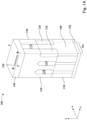
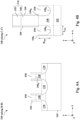
- FIG. 1A illustrates an isometric view of semiconductor device 100, according to some embodiments.
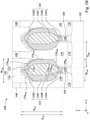
- Fig. IB illustratesa cross-sectional view along a source/drain (S/D) region (e.g., line B-B of Fig. 1A ) of semiconductor device 100, according to some embodiments.
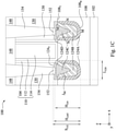
- Fig. 1C illustrates a cross-sectional view along a channel direction (e.g., line C-C of Fig. 1A ) of semiconductor device 100, according to some embodiments.
- Figs. 1A illustrates an isometric view of semiconductor device 100, according to some embodiments.
- Fig. IB illustratesa cross-sectional view along a source/drain (S/D) region (e.g., line B-B of Fig. 1A ) of semiconductor device 100, according to some embodiments.
- Fig. 1C illustrates a cross-sectional view along a channel direction (e.g., line C-C of Fig. 1A
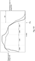
- FIG. 1D and IE respectively illustrate atomic concentrations of dopants and a semiconductor material (e.g., germanium) along the S/D region (e.g., line B-B of Fig. 1A ) and along the channel direction (e.g., line C-C of Fig. 1A ) of semiconductor device 100, according to some embodiments.
- a semiconductor material e.g., germanium
- S/D region e.g., line B-B of Fig. 1A
- the channel direction e.g., line C-C of Fig. 1A
- semiconductor device 100 can be included in a microprocessor, memory cell, or other integrated circuit (IC).
- FET 101 shown in Figs. 1A-1C is a fin field effect transistor (finFET)
- FET 101 can be agate-all-around (GAA) FET, according to some embodiments.
- substrate 102 can be a semiconductor material, such as silicon.
- substrate 102 can include a crystalline silicon substrate (e.g., wafer).
- substrate 102 can include (i) an elementary semiconductor, such as silicon (Si) or germanium (Ge); (ii) a compound semiconductor including silicon carbide (SiC), gallium arsenide (GaAs), gallium phosphide (GaP), indium phosphide (InP), indium arsenide (InAs), and/or indium antimonide (InSb); (iii) an alloy semiconductor including silicon germanium carbide (SiGeC), silicon germanium (SiGe), gallium arsenic phosphide (GaAsP), gallium indium phosphide (InGaP), gallium indium arsenide (InGaAs), gallium indium arsenic phosphide (InGaAsP),
- substrate 102 can be doped depending on design requirements (e.g., p-type substrate or n-type substrate).
- substrate 102 can be doped with p-type dopants (e.g., boron (B), indium (In), aluminum (Al), or gallium (Ga)) or n-type dopants (e.g., phosphorus (P) or arsenic (As)).
- p-type dopants e.g., boron (B), indium (In), aluminum (Al), or gallium (Ga)
- n-type dopants e.g., phosphorus (P) or arsenic (As)
- FET 101 can include a fin structure 108 extending along an x-direction, a gate structure 110 traversing through fin structure 108 along ay-direction, and S/D regions 124 formed over portions of fin structure 108.
- Fig. 1A shows fin structure 108 accommodating one FET 101, any number of FETs 101 can be disposed along fin structure 108.
- FET 101 can include multiple fin structures 108 extending along a first horizontal direction (e.g., in the x-direction)and gate structure 110 traversing through the multiple fin structures 108 along a second horizontal direction (e.g., in they-direction).
- Fin structure 108 can be formed over substrate 102 and can include a material similar to substrate 102.
- fin structure 108 can include a material (e.g., silicon germanium) having a lattice constant substantially equalto (e.g., lattice mismatch within 5%) that of substrate 102.
- fin structure 108 can include a material (e.g., silicon) identical to substrate 102.
- fin structure 108 can include multiple channel layers under gate structure 110, each made of identical or different materials from each other.Fin structure 108 can be p-type doped, n-type doped, or un-doped.
- a portion of fin structure 108 wrapped by gate structure 110 and another portion of fin structure 108 adjacent to gate structure 110 can be doped differently.
- Semiconductor device 100 can further include shallow trench isolation (STI) regions 138 configured to provide electrical isolation betweenfin structures 108 .
- STI regions 138 can provide electrical isolation between FET 101 and neighboring active and passive elements (not shown in Fig. 1A ) integrated with or deposited on substrate 102.
- STI regions 138 can include one or more layers of dielectric material, such as a nitride layer, an oxide layer disposed on the nitride layer, and an insulating layer disposed on the nitride layer.
- the insulating layer can include silicon oxide, silicon nitride, silicon oxynitride, fluorine-doped silicate glass (FSG), a low-k dielectric material, and/or other suitable insulating materials. Based on the disclosure herein, other dielectric materials for STI region 138 are within the scope and spirit of this disclosure.
- gate structure 110 can be multi-layered structures that wrapsaround portions of fin structure 108 to modulate FET 101.
- gate structure 110 can be a gate-all-around (GAA) structure, where FET 101 can be a GAA FET 101.
- GAA gate-all-around
- Gate structure 110 can include a gate dielectric layer 112, a gate electrode 114 disposed on dielectric layer 112, and gate spacers 104 disposed on sidewalls of gate electrode 114.
- Gate dielectric layer 112 can be wrapped around portions of fin structure 108 and can be further disposed between gate electrode 114 and S/D regions 124 to prevent an electrical short in between.Gate dielectric layer 112 can include any suitable dielectric material with any suitable thickness that can provide channel modulation for FET 101.
- gate dielectric layer 112 can include silicon oxide and a high-k dielectric material (e.g., hafnium oxide or aluminum oxide), and gate dielectric layer 112 can have a thickness ranging from about 1 nm to about 5 nm. Based on the disclosure herein, other materials and thicknesses for gate dielectric layer 112 are within the scope and spirit of this disclosure.
- Gate electrode 114 can function as a gate terminal for FET 101. Gate electrode 114 can include a metal stack wrapping around portions of fin structure 108. Gate electrode 114 can include any suitable conductive material that provides a suitable work function to modulate FET 101. In some embodiments, gate electrode 114 can include titanium nitride, tantalum nitride, tungsten nitride, titanium, aluminum, copper, tungsten, tantalum, copper, or nickel (Ni). Based on the disclosure herein, other materials for gate electrode 114 are within the scope and spirit of this disclosure.
- Gate spacer 104 can be in physical contact with gate electrode 114 and /or gate dielectric layers 112. In some embodiments, gate spacer 104 can be formed over fin structure 108 's side surfaces. Gate spacer 104 can have a low-k material with a dielectric constant less than about 3.9.For example, gate spacer 104 can include insulating material, such as silicon oxide, silicon nitride, a low-k material, and a combination thereof. In some embodiments, gate spacer 104 can have a thickness ranging from about 2 nm to about 10 nm. Based on the disclosure herein, othermaterials and thicknesses for gate spacer 104 are within the scope and spirit of this disclosure.
- FET 101 can have S/D regions 124 formed over fin structure 108 and over opposite sides (e.g., along x-direction) of gate structure 110 .
- Each S/Dregion 124 can include an epitaxially-grown semiconductor material.
- the epitaxially-grown semiconductor material can be the same material as the material of substrate 102.
- the epitaxially-grown semiconductor material can have a lattice constant substantially equal to (e.g., lattice mismatch within 5%) that of the material of substrate 102 .
- the epitaxially-grown semiconductor material can include (i) an elemental semiconductor material, such as Geand Si; (ii) a compound semiconductor material, such as GaAs and AlGaAs; or (iii) a semiconductor alloy, such as SiGe and GaAsP.
- the epitaxially-grown semiconductor material of S/D region 124 can be doped with p-type dopants,n-type dopants, or intrinsic dopants.
- the p-type dopants can include boron, indium, aluminum,gallium,zinc, beryllium, or magnesium.
- the n-type dopants can include phosphorus,arsenic, sulfur, or selenium.
- the intrinsic dopants can include iron or chromium.
- semiconductor device 100 's S/D regions 124 can have different materials and/or doping types from each other.
- S/D region 124 can be a bar-shape structure that extends along a vertical direction substantially perpendicular to substrate 102 and shrinks along a lateral direction substantially perpendicular to fin structure 108.
- S/D region 124 canhave a reduced lateral dimension (e.g., width in the y-direction) to avoid or reduce the RSD loss during the fabrication process of trench conductor structure 150 (discussed below at method 200).
- S/D region 124 can have an enhanced vertical dimension (e.g., height in the z-direction) to enlarge S/D region 124 's volume to provide sufficient stress to enhance FET 101 's channel mobility.In some embodiments, as shown in Fig.
- S/D region 124 's height H 124 can be greater than S/D region 124' s width W 124 to avoid the RSD loss and provide sufficient stress to enhance FET 101's channel.
- Height H 124 can be a vertical (e.g., in the z-direction) separation between S/D region 124 's top surface 124 T and S/D region 124' s bottom surface.
- height H 124 can be a vertical (e.g., in the z-direction) separation between the proximity of top surface 124 T ' s topmost vertex and the proximity of S/D region 124 's bottommost vertex.
- proximity can refer to an area within a distance of about 1 nm, about 5 nm, about 10 nm, about 20 nm, about 50 nm, or about 100 nm of a target point.
- top surface 124 T 's topmost vertex can be in contact with silicide layer 152 (discussed below).
- Width W 124 can be a lateral (e.g., in the y-direction) separation between S/D region 124's two opposite side surfaces 124 S1A and 124 S1B .
- width W 124 can be a lateral (e.g., in the y-direction) separation between the proximity of side surface 124 S1A 's outermost vertex and the proximity of side surface 124 S1B 's outermost vertex.
- a ratio of height H 124 to width W 124 can be greater than about 1.0, greater than about 1.5, greater than about 2.0, greater than about 3.0, or greater than about 5.0. If the ratio of height H 124 to width W 124 is below the above-noted lower limits, S/D region 124 may be susceptible to RSD loss and/or may not provide sufficient stress to drive FET 101's channel.
- S/D region 124 with the reduced lateral dimension (e.g., width in the y-direction) and the enhanced vertical dimension (e.g., height in the z-direction) can avoid the RSD merging between two adjacent fin structures 108 with a tight spacing.
- two adjacent S/D regions 124 with the reduced lateral dimension and the enhanced vertical dimension can be separated from each other, where the respective two underlying fin structures 108 can be separated from each other with a lateral (e.g., in the y-direction) separation S 108 from about 10 nm to about 120nm, from about 20 nm to about 100 nm, or from about 30 nm to about 80 nm.
- separation S 108 is greater than the above-noted upper limits, semiconductor device 100 may not meet the fin pitch requirementdetermined by the respective technology node (e.g., fin pitch may be required to be less than about 60 nm for a 22 nm technology node), thus failing the product requirement of the IC. If separation S 108 is less than the above-noted lower limits, semiconductor device 100 may have unintentionally merged fin structures 108 due to the limit of the lithography capability.
- two adjacent S/D regions 124 can be separated from each other, where (i) a first ratio of width W 124 to separation S 108 can be from about 0.1 to about 2.0, from about 0.2 to about 1.0, or from about 0.3 to about 0.8, and (ii) a second ratio of height H 124 to width W 124 can be greater than about 1.0, greater than about 1.5, greater than about 2.0, greater than about 3.0, or greater than about 5.0.
- ILD layer 130 may not be filled between the two laterally adjacent S/D regions 124 If the first ratio of width W 124 to separation S 108 is below the above-noted lower limits,semiconductor device 100 may not meet the fin pitch requirement determined by the respective technology node (e.g., fin pitch may be required to be less than about 60 nm for a 22 nm technology node), thus failing the product requirement of the IC.
- S/D region 124 may not provide sufficient stress to driveFET 101's channel.
- two adjacent S/D regions 124 can be separated from each other, where (i) a third ratio of width W 124 to separation S 108 can be less than about 2.0, less than about 1.0, or less than about 0.8, and (ii) a fourth ratio of height H 124 to separation S 108 can be greater than about 0.8, greater than about 1.0, or greater than about 1.5.
- ILD layer 130 may not be filled between the two laterally adjacent S/D regions 124 . If the fourth ratio of height H 124 to separation S 108 is below the above-noted lower limits, S/D region 124 may not provide sufficient stress to driveFET 101's channel.
- portions of S/D region 124's top surface 124 T can be in contact with ILD layer 130 (discussed below) and separate from S/D region 124's bottom surface with a height H 124T , where a ratio of height H 124T to width W 124 can be greater than about 1.0, greater than about 1.5, greater than about 2.0, greater than about 3.0, or greater than about 5.0. If the ratio of height H 124T to width W 124 is below the above-noted lower limits, S/D region 124 may be susceptible to RSD loss and/or may not provide sufficient stress to drive FET 101's channel.
- S/D region 124 can extend along a horizontal direction (e.g., in the x-direction) parallel to fin structure 108 with a length L 124 , where a ratio of length L 124 to width W 124 (shown in Fig. 1B ) can befrom about 0.05 to about 1.5, from about 0.1 to about 1.0, or from about 0.2 to about 1.0. If the ratio of L 124 to width W 124 is below the above-noted lower limits, ILD layer 130 (discussed below) may not be filled between the two laterally adjacent S/D regions 124.
- semiconductor device 100 may not meet the fin pitch requirementdetermined by the respective technology node(e.g., fin pitch may be required being less than about 60 nm for the technology node of 22 nm), thus failing the product requirement of the IC.
- S/D region 124 can be a layer stack of epitaxially-grown semiconductor material.
- S/D region can include a first layer 124A formed in fin structure 108.
- First layer 124A can extend from fin structure 108's first top surface 108 T (shown in Fig. 1C ) towards fin structure 108's second top surface 108 B , where first top surface 108 T can be higher than second top surface 108 B .
- first top surface 108 T and/or second top surface 108 B can be substantially parallel to substrate 102.
- first layer 124A's bottom surface can be substantially coplanar and in contact with second top surface 108 B .
- first layer 124A's bottom surface can be S/D region 124's bottom surface.
- first layer 124A's top surface can be below or substantially coplanar with portions of gate spacer 104 that is over fin structure 108's side surfaces.
- First layer 124A can be made of an epitaxially-grown semiconductor material, such as a compound semiconductor material (e.g., SiGe).
- first layer 124A can be made of SiGe with the atomic concentration of germanium less than about 35%, such as from about 5% to about 30%, to reduce crystal defects of second layer 124B and third layer 124C (discussed below).
- first layer 124A can be made of SiGe with a substantially constant atomic concentration of germanium or a gradient atomic concentration of germanium (shown in Figs. 1D and IE that respectively illustrate S/D region 124's atomic concentration of germanium along Fig. 1C 's line M-M and Fig. 1C 's line N-N)gradually increasing along a direction away from fin structure 108.
- First layer 124A can be doped with p-type dopants, such asboron, indium, aluminum, gallium, zinc, beryllium, and magnesium. In some embodiments, first layer 124A can be doped with p-type dopants having a doping concentration less than 5 ⁇ 10 20 /cm 3 , such as from about 5 ⁇ 10 19 /cm 3 to about 5 ⁇ 10 20 /cm 3 , to mitigate short channel effects of FET 101. In some embodiments, first layer 124A can be doped with p-type dopants having a substantially constant doping concentration or a gradient doping concentration(shown in Figs. 1D and IE that respectively illustrate S/D region 124's doping concentration along Fig.
- p-type dopants such asboron, indium, aluminum, gallium, zinc, beryllium, and magnesium.
- first layer 124A can be doped with p-type dopants having a doping concentration less than 5 ⁇ 10 20
- first layer 124A can be doped with n-type dopants, such as phosphorus and arsenic, or intrinsic dopants, such as iron and chromium.
- S/D region 124 can further include a second layer 124B formed over first layer 124A.
- Second layer 124B can be made of a compound semiconductor, such as SiGe.
- first and second layers 124A and 124B can be made of SiGe, where second layer 124B can have a greater atomic concentration of germanium than first layer 124A to provide stress to enhance FET 101's channel mobility.
- second layer 124B can be made of SiGe with the atomic concentration of germanium from about 30% to about 50%.
- second layer 124B can be made of SiGewith a substantially constant atomic concentration of germanium or an atomic concentration of germanium (shown in Figs.
- Second layer 124B can be doped with p-type dopants, such asboron, indium, aluminum, gallium, zinc, beryllium, and magnesium. Second layer 124B can be doped having a greater doping concentration than first layer 124A to provide a low contact resistance for FET 101.
- p-type dopants such asboron, indium, aluminum, gallium, zinc, beryllium, and magnesium. Second layer 124B can be doped having a greater doping concentration than first layer 124A to provide a low contact resistance for FET 101.
- second layer 124B can be doped with p-type dopants having a doping concentration greater than or substantially equal to about 5 ⁇ 10 20 /cm 3 , such as from about 5 ⁇ 10 20 /cm 3 to about 1 ⁇ 10 21 /cm 3 , to provide a low contact resistance for FET 101 .
- second layer 124B can be doped with p-type dopants having a substantially constant doping concentration or a gradient doping concentration (shown in Figs. 1D and IE) gradually increasing along a direction away from first layer 124A .
- second layer 124B can be doped with n-type dopants, such as phosphorus and arsenic, or intrinsic dopants, such as iron and chromium.
- S/D region 124 can further include a third layer 124C formed over second layer 124B.
- Third layer 124C can be made of a compound semiconductor, such as SiGe.
- second and third layers 124B and 124C can be made of SiGe, where third layer 124C can have anatomic concentration of germanium greater than or substantially equal tosecond layer 124B to provide stress to enhance FET 101's channel mobility.
- third layer 124C can be made of SiGe with the atomic concentration of germanium from about 45% to about 65%.
- third layer 124C can include SiGewith a substantially constant atomic concentration of germanium or an atomic concentration of germanium (shown in Figs.
- third layer 124C's volume can have be greater than first layer 124A's volume and/or second layer 124B's volume to provide stress to enhance FET 101's channel mobility.
- hird layer 124C can be doped with p-type dopants, such asboron, indium, aluminum, gallium, zinc, beryllium, and magnesium.
- Third layer 124C can be doped with a substantially equal or a greater doping concentration than first layer 124A and/or second layer 124B to provide a low contact resistance for FET 101.
- third layer 124C can bedoped with p-type dopants having a doping concentration greater than or substantially equal to about 1 ⁇ 10 21 /cm 3 , such as from about 1 ⁇ 10 21 /cm 3 to about 3 ⁇ 10 21 /cm 3 , to provide a low contact resistance for FET 101.
- third layer 124C can be doped with p-type dopants having a substantially constant doping concentration or a gradient doping concentration (shown in Figs. 1D and IE) gradually increasing along a direction away from second layer 124B.
- third layer 124C can be doped with n-type dopants, such as phosphorus and arsenic, or intrinsic dopants, such as iron and chromium.
- n-type dopants such as phosphorus and arsenic
- intrinsic dopants such as iron and chromium.
- at least one of S/D region 124's side surfaces 124 S1A and 124 S1B can be made of third layer 124C.
- side surfaces 124 S1A and 124 S1B can be in contact with (ILD) layer 130 (discussed below) and/or in contact with silicide layer 152 (discussed below).
- side surfaces 124 S1A and 124 S1B can be substantially perpendicular to substrate 102.
- side surfaces 124 S1A and 124 S1B can be (110) crystal planes.
- S/D region 124 can further include side surfaces 124 S3A and 124 S3B proximate to S/D region 124's bottom surface (e.g., such as proximate to second top surface 108 B ), where side surfaces 124 S3A and 124 S3B can be made of third layer 124C.
- side surfaces 124 S3A and 124 S3B can be (111) crystal planes.
- side surfaces 124 S3A and 124 S3B can be in contact with gate spacers 104 that are formed over fin structure 108's side surfaces.
- side surfaces 124 S3A and/or 124 S3B can be separated from gate spacers 104 that are formed over fin structure 108's side surfaces.
- S/D region 124 can further include a capping layer 124D formed over third layer 124C.
- capping layer 124D's top surface can be S/D region 124's top surface 124 T .
- top surface 124 T can include (111) or (100) crystal planes.In some embodiments, top surface 124 T can be free from (100) crystal planes (e.g., top surface 124 T only includes (111) crystal planes).
- Capping layer 124D can be made of a compound semiconductor, such as SiGe.
- third layer 124C and capping layer 124D can be made of SiGe, where capping layer 124D can have anatomic concentration of germanium less than or substantially equal to third layer 124C to form a silicide layer 152 (discussed belowat method 200) with a low sheet resistance.
- capping layer 124D can be made of SiGe with the atomic concentration of germanium less than about 60%, such as from about 40% to about 60%.
- capping layer 124D can include SiGe with a substantially constant atomic concentration of germanium or a gradient atomic concentration of germanium (shown in Fig. ID) gradually increasing along a direction away from third layer 124C.
- Capping layer 124D can be doped with p-type dopants, such asboron, indium, aluminum, gallium, zinc, beryllium, and magnesium. Capping layer 124D can be doped with any suitable doping concentration to provide a low contact resistance for FET 101. In some embodiments, capping layer 124D can be doped with p-type dopants having a doping concentration from to about 5 ⁇ 10 20 /cm 3 to about 2 ⁇ 10 21 /cm 3 to provide a low contact resistance for FET 101. In some embodiments, capping layer 124D can be doped with p-type dopants having a substantially constant doping concentration or a gradient doping concentration (shown in Fig.
- capping layer 124D and first layer 124A can be doped with p-type dopants, where the doping concentration of capping layer 124D can be greater the doping concentration of first layer 124A.
- capping layer 124D and second layer 124B can be doped with p-type dopants, where the doping concentration of capping layer 124D can be substantially equal to the doping concentration of second layer 124B.
- first layer 124A, second layer 124B, third layer 124C, and capping layer 124D can be doped with p-typedopants, where the doping concentration of third layer 124C can be greater than those of first layer 124A, second layer 124B, and capping layer 124D.
- capping layer 124D can be doped with n-type dopants, such as phosphorus and arsenic, or intrinsic dopants, such as iron and chromium.
- S/D region 124 can further include side surfaces 124 S2A and 124 S2B proximate to S/D region 124's top surface 124 T , where side surfaces 124 S2A and 124 S2B can be made of capping layer 124D.
- side surfaces 124 S2A and 124 S2B can be (111) crystal planes.
- side surfaces 124 S2A and 124 S2B can be in contact with an interlayer dielectric (ILD) layer 130 (discussed below) and/or silicide layer 152 (discussed below).
- ILD interlayer dielectric
- S/D region 124's side surfaces 124 S1A and/or 124 S1B can be made of capping layer 124D.
- Semiconductor device 100 can further include an interlayer dielectric (ILD) layer 130 to provide electrical isolation to structural elements it surrounds or covers, such as gate structure 110 and S/D regions 124.
- ILD interlayer dielectric
- two laterally (e.g., in the y-direction) adjacent S/D regions 124 may need to be separated greater than or substantially equal to about 3 nm or about 5 nm to ensure ILD layer 130 being formed between the two laterally adjacent S/D regions 124. If the above-noted separation is below the above-noted lower limits, ILD layer 130 may not be able to be formed between the two laterally adjacent S/D regions 124 due to the gap fill limitation of the deposition process (discussed at operation 230) associated with ILD layer 130.
- ILD layer 130 can include any suitable dielectric materialto provide electrical insulation, such as silicon oxide, silicon dioxide, silicon oxycarbide, silicon oxynitride, silicon oxy-carbon nitride, and silicon carbonitride. ILD layer 130 can have any suitable thickness, such as from about 50 nm to about 200 nm, to provide electrical insulation. Based on the disclosure herein, other insulating materials and thicknesses for ILD layer 130 are within the scope and spirit of this disclosure.
- Semiconductor device 100 can further include a layer of insulating material 148 formed over gate structure 110 and ILD layer 130.
- Layer of insulating material 148 can be further formed over S/D region 124, and trench conductor structure 150 can be formed throughlayer of insulating material 148 to contact S/D region 124 .
- Layer of insulating material 148 can be made of any suitable insulating material, such as silicon oxide, silicon nitride, a low-k dielectric material, and a high-k dielectric material.
- layer of insulating material 148 can be made of any suitable thickness, such as from about 10 nm to about 400nm, that can provide sufficient electrical insulation between FETs 101 and an interconnect structure (not shown in Figs. 1A-1C ) formed over FETs 101. Based on the disclosure herein, other insulating materials and thicknesses for layer of insulating material 148 are within the scope and spirit of this disclosure.
- Semiconductor device 100 can further include a trench conductor structure 150 formed through layer of insulating material 148.
- Trench conductor structure 150 can electrically connect FET 101's S/D region 124 to the interconnect structure (not shown in Figs. 1A-1C ) formed over FET 101.
- Trench conductor structure 150 can have a lateral width W 150 from about 5 nm to about 40 nm, from about 8 nm to about 30 nm, or from about 8 nm to about 25 nm. If width W 150 is below the above-noted lower limits, the contact resistance between trench conductor layer 150 and S/D region 124 may be increased to degrade FET 101's performance.
- width W 150 is beyond the above-noted upper limits, semiconductor device 100 may not meet the fin pitch requirement determined by the respective technology node (e.g., fin pitch may be required to beless than about 60 nm for a 22 nmtechnology node), thus failing the product requirement of the IC.Further, because S/D region 124 can have a reduced lateral dimension (e.g., width W 124 ) to avoid or reduce the RSD loss, trench conductor structure 150 cancontact a majority of S/D region 124's top surface 124 T .
- a ratio oftrench conductor structure 150's width W 150 to S/D region 124's width W 124 can be from about 0.5 to about 1.5, from about 0.7 to about 1.3, from about 0.7 to about 1.2, from about 0.8 to about 1.1, or from about 0.9 to about 1.1.
- width W 150 to width W 124 is below the above-noted lower limits (e.g., S/D region 124's width W 124 is too wide), S/D region 124 may be susceptible to RSD loss and/or may not provide sufficient stress to drive FET 101's channel. If the ratio of width W 150 to width W 124 is beyond the above-noted upper limits (e.g., trench conductor structure 150's width W 150 is too wide), semiconductor device 100 may not meet the fin pitch requirement determined by the respective technology node (e.g., fin pitch may be required to be less than about 60 nm for a 22 nm technology node), thus failing the product requirements of the IC.
- trench conductor structure 150's width W 150 can be greater than S/D region 124's width W 124 , and trench conductor structure 150 can contact a majority of S/D region 124's side surfaces 124 S1A , 124 S1B , 124 S2A , and/or 124 S
- trench conductor structure 150 can contact more than about 50%, more than about 70%, or more than about 90% of the areas of side surfaces 124 S1A , 124 S1B , 124 S2A , and/or 124 S2B .
- trench conductor structure 150 can connect FET 101's gate structure 110 to the interconnect structure formed over FET 101.
- trench conductor structure 150 can protrude into S/D region 124.
- trench conductor structure 150 can include a silicide layer 152 protruding S/D region 124 and a layer of conductive material 154 formed over silicide layer 152.
- Silicide layer 152 can include a metal silicide material to provide a low resistance interface between layer of conductive material 154 and S/D region 124.
- silicide layer 152 can be formed over and in contact with S/D region 124's top surface 124 T to provide a low resistance interface between layer of conductive material 154 and S/D region 124.
- silicide layer 152 can be formed and in contact with the proximities of top surface 124 T 's topmost vertex to provide a low resistance interface between layer of conductive material 154 and S/D region 124.
- silicide layer 152 can be formed over and in contact with S/D region 124's side surfaces 124 S2A and 124 S2B that are proximate to S/D region 124's top surface 124 T . In some embodiments, silicide layer 152 can be formed over and in contact with at least one of S/D region 124's side surfaces 124 S1A and 124 S1B .
- the metal silicide material for silicide layer 152 can include titanium, cobalt, nickel, platinum, palladium, tungsten, molybdenum, tantalum, vanadium, chromium, silicon, or germanium.Layer of conductive material 154 can include any suitable conductive material that provide low resistance between silicide layer 152 and the interconnect structure (not shown in Figs.
- layer of conductive material 154 can include a metallic material, such as copper, tungsten, aluminum, and cobalt.
- layer of conductive material 154 can further include a stack of conductive materials (not shown in Figs. 1A-1C ), such as a conductive nitride material (e.g., titanium nitride or tantalum nitride), that can act as a diffusion barrier, an adhesion promotion layer, or a nucleation layer to embed theabove-noted metallic materials in layer of insulating material 148.
- a conductive nitride material e.g., titanium nitride or tantalum nitride
- silicide layer 152 can be formed protruding S/D region 124's capping layer 124D, where S/D region 124's top surface 124 T can be made of capping layer 124D. In some embodiments, silicide layer 152 can be formed through S/D region 124's capping layer 124D and protruding S/D region 124's third layer 124C, where S/D region 124's top surface 124 T can be made of third layer 124C (not shown in Figs. 1B and 1C ).
- silicide layer 152 can be formed through S/D region 124's capping layer 124D and third layer 124C, and protruding S/D region 124's second layer 124B, where S/D region 124's top surface 124 T can be made of second layer 124B (not shown in Figs. 1B and 1C ).
- separation S 152 can be a vertical (e.g., in the z-direction) separation between S/D region 124's bottom surface and the proximity of topmost vertex of silicide layer 152's top surface, where a ratio of separation S 152 to width W 124 can be greater than about 1.0, greater than about 1.5, greater than about 2.0, greater than about 3.0, or greater than about 5.0. If the ratio of separation S 152 to width W 124 is below the above-noted lower limits, S/D region 124 may be susceptible to RSD loss and/or may not provide sufficient stress to drive FET 101's channel.
- Fig. 2 is a flow diagram of a method 200 for fabricating semiconductor device 100, according to some embodiments.
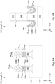
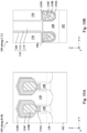
- the operations illustrated in Fig. 2 will be described with reference to the example fabrication process for fabricating semiconductor device 100 as illustrated in Figs. 3A-8A , 3B-8B , 9 , 10A-11A , and 10B-11B .
- Figs. 3A-8A and 10A-11A illustrate cross-sectional views along lines B-B of structure of Fig. 1A at various stages of its fabrication, according to some embodiments.
- Figs. 3B-8B and 10B-11B illustrate cross-sectional views along lines C-C of structure of Fig. 1A at various stages of its fabrication, according to some embodiments.
- FIG. 9 illustrates the growth temperatures for epitaxially growingS/D region 124 in method 200, according to some embodiments.Operations can be performed in a different order or not performed depending on specific applications. Method 200 may not produce a complete semiconductor device 100. Accordingly, it is understood that additional processes can be provided before, during, and/or after method 200, and that some other processes may be briefly described herein. Further, the discussion of elements in Figs. 1A-1E , 3A-8A , 3B-8B , 9 , 10A-11A, and 10B-11B with the same annotations applies to each other, unless mentioned otherwise.
- a recess structure is formed adjacent to a sacrificial gate structure.
- a recess structure 436 (shown in Figs. 4A and 4B ) can be formed over substrate 102 and adjacent to a sacrificial gate structure 310 with reference to Figs. 3A-4A and 3B-4B .
- the process of forming recess structure 436 can include (i) forming fin structures 108 (shown in Figs. 3A and 3B ) with a width W 108 over substrate 102; (ii) forming sacrificial gate structures 310 (shown in Figs. 3A and 3B ) over fin structures 108; and (iii) removing fin structures 108 through sacrificial gate structures 310 to form recess structure 436.
- the process of forming fin structures 108 can include (i) providing substrate 102; (ii) etching substrate 102 through a patterned mask layer (not shown in Figs. 3A and 3B )using an etch process to define fin structure 108's width W 108 ; and (iii) forming STI region 138 over the etched substrate 102 using a deposition process and an etch back process.
- the process of forming fin structures 108 can include (i) epitaxially growing a channel layer (e.g., a SiGe layer) over substrate 102 using an epitaxial growth process, and (ii) etching the channel layer through the patterned mask layer (not shown in Figs.
- the etch process can include a dry etch process or a wet etch process.
- the dry etch process can include using any suitable etchant,such as an oxygen-containing gas, a fluorine-containing gas, a chlorine-containing gas, and a bromine-containing gas
- the wet etch process can include etching in any suitable wet etchant, such as diluted hydrofluoric acid, potassium hydroxide solution, ammonia, and nitric acid.
- the resulting fin structure 108's width W 108 can be any suitable width, such as from about 5nm to about 30 nm, that can provide short channel control for FET 101.
- width W 108 can be substantially equal to fin structure 108's width after method 200.
- the deposition process for forming STI region 138 can include any suitable growth process, such as a physical vapor deposition (PVD) process, a chemical vapor deposition (CVD) process, a high-density-plasma (HDP) CVD process, a flowable CVD (FCVD) process, and an atomic layer deposition (ALD) process.
- PVD physical vapor deposition
- CVD chemical vapor deposition
- HDP high-density-plasma
- FCVD flowable CVD
- ALD atomic layer deposition
- the etch back process for forming STI region 138 can include a dry etch process, a wet etch process, or a polishing process, such as chemical vapor deposition (CMP) process.
- CMP chemical vapor deposition
- the process of forming sacrificial gate structure 310 can include (i) blanket depositing a polysilicon layer 348 and a hard mask layer 350 over fin structures 108 using a suitable deposition process, such as a CVD process, a PVD process, and an ALD process; (ii) removing polysilicon layer 348 and hard mask layer 350 through a patterned mask layer (not shown in Figs. 3A and 3B ) using an etching process; and (iii) forming gate spacers 104 over side surfaces of polysiliconlayer 348 and/or over fin structure 108's side surfaces using a suitable deposition process and an etch process.Based on the disclosure herein, other processes for forming gate structures 310 are within the spirit and scope of this disclosure.
- recess structure 436 can be formed by removing fin structures 108 through sacrificial gate structures 310 using an etching process.
- the etching process can include a dry etch process or a wet etch process. In some embodiments, the etching process can be a time-etch process.
- the dry etch process can include using any suitable etchant,such as an oxygen-containing gas, a fluorine-containing gas, a chlorine-containing gas, and a bromine-containing gas
- the wet etch process can include etching in any suitable wet etchant, such as diluted hydrofluoric acid, potassium hydroxide solution, ammonia, and nitric acid.
- suitable wet etchant such as diluted hydrofluoric acid, potassium hydroxide solution, ammonia, and nitric acid.
- the resulting recess structure 436 can span with length L 124 associated with two adjacent sacrificial gate structure 310's separation. Further, the resulting recess structure 436 can protrude in fin structure 108with a depth H 436 to define first top surface 108 T outside recess structure 436 and second top surface 108 B within recess structure 436.
- depth H 436 can be less than or substantially equal to S/D region 124's height H 124 (shown in Figs. 1B and 1C ).
- the resulting recess structure 436 can protrude into fin structure 108 to form second top surface 108 B vertically (e.g., in the z-direction) below gate spacers 104 that are formed over fin structure 108's side surface.
- first layer 124A (shown in Figs. 5A and 5B ) can be formed in recess structure 436 of Fig. 4 with reference to Figs. 5A, 5B , and 9 .
- the process of forming first layer 124A can include (i) annealing the structure of Fig. 4A to desorb contaminants (e.g., hydrocarbon) from recess structure 436's surface with a suitable annealing temperature T pre (shown in Fig. 9 ), such as about 200°C; (ii) annealing the structure of Fig.
- annealing temperature T bake can be greater than annealing temperature T pre and growth temperature T L1 to effectively desorb native oxides from recess structure 436.
- the epitaxial growth process for first layer 124A can include (i) a CVD process, such as a low pressure CVD (LPCVD) process, a rapid thermal CVD (RTCVD) process, a metal-organic CVD (MOCVD) process, an atomic layer CVD (ALCVD) process, an ultrahigh vacuum CVD (UHVCVD) process, and a reduced pressure CVD (RPCVD) process; (ii) a molecular beam epitaxy (MBE) process; (iii) an epitaxial deposition/partial etch process, such as a cyclic deposition-etch (CDE) process; or (iv) a selective epitaxial growth (SEG) process.
- a CVD process such as a low pressure CVD (LPCVD) process, a rapid thermal CVD (RTCVD) process, a metal-organic CVD (MOCVD) process, an atomic layer CVD (ALCVD) process, an ultrahigh vacuum CVD (UHVCV
- the epitaxial growth process can be performed using suitable lower-order precursors or higher-order precursorsto epitaxially grow the semiconductor material for first layer 124A.
- Lower-order precursor and a higher-order precursor can include a common chemical element (e.g., Si or Ge) as S/D region 124, where the higher-order precursor can have a greater molecular weight than the lower-order precursor.
- first layer 124A can include SiGe, where the respective lower-order precursor can include silane (SiH 4 ), disilane (Si 2 H 6 ), dichlorosilane (DCS), or germane (GeH 4 ), and the respective higher-order precursor can include disilane (Si 2 H 6 ), trisilane (Si 3 H 8 ), or digermane (Ge 2 H 6 ).
- the epitaxial growth process for first layer 124A can have a higher growth rate over a (100) crystal plane thanover the (110) or (110) crystal plane by solely using the higher-order precursor in the epitaxial growth process.
- the epitaxial growth process for first layer 124A can further include doping the grown semiconductor material with p-type dopants or n-type dopants.
- the epitaxial growth process can be performed using suitable dopant precursors, such as diborane (B 2 H 6 ), boron difluoride (BF 2 ), and boron trifluoride (BF 3 ), to dope boron (e.g., a p-type dopant) in first layer 124A with a suitable doping concentration.
- the epitaxial growth process for first layer 124A can result in doped first layer 124A of vertical thickness H 124A measured from second top surface 108 B .
- the epitaxial growth process for first layer 124A can result in first layer 124A with vertical thickness H 124A greater than first layer 124's width W 108 , because the epitaxial growth process can epitaxiallygrow first layer 124A with a faster growth rate over the (100) crystal plane (e.g., over second top surface 108 B ) than over the (110) or (111) crystal planes (e.g., over recess structure 436's side surfaces).
- first layer 124A's thickness H 124A can be substantially equal to first layer 124A's thickness of the resulting S/D region 124 (shown in Figs.
- first layer 124A can result in first layer 124A with a top surface T 124A substantially parallel to substrate 102.
- first layer 124A's top surface T 124A can include a (100) crystal plane.
- first layer 124A's top surface T 124A can be vertically (e.g., in the z-direction) below or substantially coplanar with gate spacers 104 formed over fin structure 108's side surfaces.
- first layer 124A can havevertical thickness H 124A less than about 20 nm, such as from about 5 nm to about 20 nm.
- second layer 124B (discussed at operation 215) may be grown on first layer 124A's side surfaces, thus resulting in second layer 124B with vertical thickness H 124B equal to or less than width W 124B which can cause S/D region 124 to be susceptible to the RSD loss or the RSD merging after method 200.
- first layer 124A may not reconcile a lattice mismatch between second layer 124B and fin structure 108, thus failing to reduce crystal defects of second layer 124B .
- the epitaxial growth process for first layer 124A can result in first layer 124A under and in contact with gate spacer 104.
- the epitaxial growth process for first layer 124A can further include applying an etching gas, such as hydrogen chloride (HCl), to etch a portion of the grown first layer 124A to expose fin structure 108's first top surface 108 T (shown in Fig. 5B ).
- an etching gas such as hydrogen chloride (HCl)
- a second epitaxial region is formed over the first epitaxial region.
- second layer 124B (shown in Figs. 6A and 6B ) can be formed over first layer 124A of Figs. 5A and 5B with reference to Figs. 6A, 6B , and 9 .
- the process of forming second layer 124B can include epitaxially growing a semiconductor material over first layer 124A using an epitaxial growth processwith a growth temperature T L21 (shown in Fig. 9 ).
- Growth temperature T L21 can be less than growth temperature T L1 to increase the epitaxial growth process's growth rate over a (100) crystal plane (e.g., overfirst layer 124A's top surface T 124A ) and decrease epitaxial growth process's growth rate over the (110) or (110) crystal planes (e.g., over first layer 124A's side surfaces).
- second layer 124B can result in second layer 124B with a width W 124B and a vertical thickness H 124B greater than width W 124B .
- second layer 124B with vertical thickness H 124B greater than width W 124B can result in S/D region 124 with height H 124 greater than width W 124 after method 200.
- a ratio of second layer 124B's height H 124B to second layer 124B's width W 124B can be greater than about 1.0, greater than about 1.5, greater than about 2.0, greater than about 3.0, or greater than about 5.0.
- growth temperature T L21 can be from about 250°C to about 550°C, from about 300°C to about 500°C, or from about 300°C to about 450°C to result in second layer 124B with vertical thickness H 124B greater than width W 124B .
- a difference between growth temperature T L1 and T L21 can be from about 100°C to about 400°C, from about 100°C to about 300°C, or from about 100°C to about 250°C.
- the epitaxial growth process may result in an amorphous second layer 124B or a polycrystalline second layer 124B, thus degrading FET 101's speed and yield. If the above-noted growth temperature difference is below the above-noted lower limits, the epitaxial growth process may provide similar growth rates over the (100) crystal plane and over (110)/(111) crystal planes, thus resulting in second layer 124B with vertical thickness H 124B equal to or less than width W 124B which can cause S/D region 124 to be susceptible to RSD loss or RSD merging.
- second layer 124A's width W 124B and thickness H 124B can be substantially equal to second layer 124B's width and thickness of the resulting S/D region 124 (shown in Figs. 1B and 1C ) after method 200.
- the epitaxial growth process for second layer 124B can include a CVD process, anLPCVD process, a RTCVD process, anMOCVD process, an ALCVD process, an UHVCVD process, a RPCVD process, anMBE process, a CDE process, or anSEG process.
- growth temperature T L21 being less than growth temperature T L1
- the growth rate (e.g., over the (100), (111), and (110) crystal planes) of the epitaxial growth process for second layer 124B can be less than the respective growth rate (e.g., over the (100), (111), and (110) crystal planes) of the epitaxial growth process for first layer 124A.
- the epitaxial growth process for second layer 124B can be performed using higher-order precursors to boost the growth rate of second layer 124B (e.g., the epitaxial growth process for second layer 124B is free from using lower-order precursors).
- the epitaxial growth process for second layer 124B can be performed solely using higher-order precursors to increase the second layer 124B's growth rate over a (100) crystal plane and decrease second layer 124B's growth rate over the (110) or (110) crystal plane, thus resulting second layer 124B with vertical thickness H 124B greater than width W 124B .
- the epitaxial growth process for second layer 124B can further include doping the grown semiconductor material with p-type dopants or n-type dopants.
- the epitaxial growth process can be performed using suitable dopant precursors, such as B 2 H 6 , BF 2 , and BF 3 to dope boron (e.g., a p-type dopant) in second layer 124B with a suitable doping concentration.
- the epitaxial growth process for second layer 124B can further include an in-situ etching process to etch a portion of the grown semiconductor material by using an etching gas, such as HCl.
- the in-situ etching process can etch (110)/(111) crystal planes with a first etch rate, and the etching process can further etch (100) crystal planes with a second etch rate.
- growth temperature T L21 being less thangrowth temperature T L1
- the first etch rate can be greater than the second etch rate.
- the resulting second layer 124B can have vertical thickness H 124B greater than width W 124B .
- the resulting second layer 124B can exhibit side surfaces with (110) and/or (111) crystal planes.
- the epitaxial growth process together with the in-situ etching process can form second layer 124B having a side surface S 124B substantially perpendicular to substrate 102, because the epitaxial growth process together with the etching process has a lower growth rate and a higher etching rate over the (110) crystal plane.
- side surface S 124B can include a (110) crystal plane.
- the epitaxial growth process together with the in-situ etching process can form second layer 124B having a side surface U 124B proximate to first layer 124A's top surface T 124A , where side surface U 124B can include a (111) crystal plane, because the epitaxial growth process together with the in-situ etching process has a lower growth rate and a higher etching rate over the (111) crystal plane.
- the epitaxial growth process together with the in-situ etching process can form second layer 124B having a top surface T 124B that can include a (100) crystal plane (proximate to top surface T 124B 's topmost vertex in Fig.
- the in-situ etching process can etch a portion of the grown second layer 124B to expose fin structure 108's first top surface 108 T (shown in Fig. 6B ).
- a third epitaxial region is formed over the second epitaxial region.
- third layer 124C (shown in Figs. 7A and 7B ) can be formed over second layer 124B of Figs. 6A and 6B with reference to Figs. 7A, 7B , and 9 .
- the process of forming third layer 124C can include epitaxially growing a semiconductor material over second layer 124B using an epitaxial growth processwith a growth temperature T L22 (shown in Fig. 9 ).
- Growth temperature T L22 can be substantially equal to or less than growth temperature T L21 to increase the epitaxial growth process's growth rate over a (100) crystal plane (e.g., overproximities of top surface T 124B ' s topmost vertex in Fig. 6A ) and decrease epitaxial growth process's growth rate over the (110) or (110) crystal planes (e.g., over second layer 124B's side surface S 124B ). Accordingly, the epitaxial growth process for third layer 124C can result in third layer 124C with a width W 124C and a vertical thickness H 124C greater than width W 124C .
- third layer 124C with vertical thickness H 124C greater than width W 124C can result in S/D region 124 with height H 124 greater than width W 124 after method 200.
- a ratio of third layer 124C's height H 124C to third layer 124C's width W 124C can be greater than about 1.0, greater than about 1.5, greater than about 2.0, greater than about 3.0, or greater than about 5.0.
- a ratio of the combination of second and third layers 124B's and 124C's heights (e.g., H 124B + H 124C ) to the combination of second and third layers 124B's and twice of 124C's widths (e.g., W 124B +2 ⁇ W 124C ) can be greater than about 1.0, greater than about 1.5, greater than about 2.0, greater than about 3.0, or greater than about 5.0.
- growth temperature T L22 can be from about 250°C to about 550°C, from about 300°C to about 500°C, or from about 300°C to about 450°C to result in third layer 124C with vertical thickness H 124C greater than width W 124C . If growth temperature T L22 is below the above-noted lower limits, the epitaxial growth process may result in an amorphous third layer 124C or a polycrystalline third layer 124C, thus degrading FET 101's speed and yield.
- a difference between growth temperature T L1 and T L22 can be from about 100°C to about 400°C, from about 100°C to about 300°C, or from about 100°C to about 250°C.
- the epitaxial growth process may result in an amorphous third layer 124C or a polycrystalline third layer 124C, thus degrading FET 101's speed and yield. If the above-noted growth temperature difference is below the above-noted lower limits, the epitaxial growth process may provide similar growth rates between the (100) crystal plane and (110)/(111) crystal planes, thus resulting in third layer 124C with vertical thickness H 124C equal to or less than width W 124C which can cause S/D region 124 to be susceptible to RSD loss or RSD merging.
- third layer 124C's width W 124C and thicknessH 124C can be substantially equal to third layer 124C's width and thickness of the resulting S/D region 124 (shown in Figs.
- the epitaxial growth process for third layer 124C can include a CVD process, anLPCVD process, a RTCVD process, anMOCVD process, an ALCVD process, an UHVCVD process, a RPCVD process, anMBE process, a CDE process, or anSEG process.
- growth temperature T L22 being substantially equal to or less than growth temperature T L21
- the growth rate (e.g., over the (100), (111), and (110) crystal planes) of the epitaxial growth process for third layer 124C can be substantially equal to or less than the respective growth rate (e.g., over the (100), (111), and (110) crystal planes) of the epitaxial growth process for second layer 124B.
- the epitaxial growth process for third layer 124C can be performed using higher-order precursors to boost the growth rate of third layer 124C (e.g., the epitaxial growth process for third layer 124C is free from using lower-order precursors).
- the epitaxial growth process for third layer 124C can be performed solely using higher-order precursors to increase the third layer 124C's growth rate over a (100) crystal plane and decrease third layer 124C's growth rate over the (110) or (110) crystal plane, thus resulting third layer 124C with vertical thickness H 124C greater than width W 124C .
- the epitaxial growth process for third layer 124C can further include doping the grown semiconductor material with p-type dopants or n-type dopants.
- the epitaxial growth process can be performed using suitable dopant precursors, such as B 2 H 6 , BF 2 , and BF 3 , to dope boron (e.g., a p-type dopant) in third layer 124C with a suitable doping concentration.
- the epitaxial growth process for third layer 124C can further include an in-situ etching process to etch a portion of the grown semiconductor material by using an etching gas, such as HCl and SiH 4 .
- the in-situ etching process can etch (110)/(111) crystal planes with a first etch rate, and the etching process can further etch (100) crystal planes with a second etch rate.
- growth temperature T L22 being substantially equal to or less than growth temperature T L21
- the first etch rate can be greater than the second etch rate.
- the resulting third layer 124C can have vertical thickness H 124C greater than width W 124C .
- the resulting third layer 124C can exhibit side surfaces with (110) and/or (111) crystal planes.
- the epitaxial growth process together with the in-situ etching process can form third layer 124C having a side surface S 124C substantially perpendicular to substrate 102, because the epitaxial growth process together with the etching process has a lower growth rate and a higher etching rate over the (110) crystal plane.
- side surface S 124C can include a (110) crystal plane.
- the epitaxial growth process together with the in-situ etching process can form third layer 124C having a side surface U 124C proximate to first layer 124A's top surface T 124A , where side surface U 124C can include a (111) crystal plane, because the epitaxial growth process together with the in-situ etching process has a lower growth rate and a higher etching rate over the (111) crystal plane.
- the epitaxial growth process together with the in-situ etching process can form third layer 124C having a top surface T 124C that can include (111) crystal planes (shown in Fig. 7A ) along the y-direction.
- top surface T 124C can be above or substantially coplanar with fin structure 108's first top surface 108 T .
- the in-situ etching process can etch a portion of the grown third layer 124C to expose fin structure 108's first top surface 108 T .
- the in-situ etching process can etch a portion of the grown third layer 124C to expose the underlying second layer 124B and/or first layer 124A (shown in Fig.
- the in-situ etching process can etch a portion of the grown third layer 124C to separate third layer 124C from gate spacer 104 (e.g., separation S 124C greater than zero, as shown in Fig. 7B ).
- a fourth epitaxial region is formed over the third epitaxial region.
- capping layer 124D (shown in Figs. 8A and 8B ) can be formed over third layer 124C of Figs. 7A and 7B with reference to Figs. 8A, 8B , and 9 .
- the process of forming capping layer 124D can include epitaxially growing a semiconductor material over third layer 124C using an epitaxial growth processwith a growth temperature T L3 (shown in Fig. 9 ).
- Growth temperature T L3 can be any suitable temperaturegreater than growth temperatures T L21 and TL 22 . In some embodiments, growth temperature T L3 can be greater than growth temperature T L1 .
- the epitaxial growth process for capping layer 124D can result in capping layer 124D with a width W 124D and a vertical thickness H 124D .
- vertical thickness H 124D can be greater than or substantially equal to width W 124D .
- capping layer 124D's width W 124D and thickness H 124D can be substantially equal to capping layer 124D's width and thickness of the resulting S/D region 124 (shown in Figs. 1B and 1C ) after method 200.
- the combination (e.g., W 124B +2 ⁇ W 124C +2 ⁇ W 124D ) of second layer 124B's width W 124B , twice of third layer 124C's width W 124C , and twice of capping layer 124D's width W 124D can be substantially equal to S/D region 124's width W 124 shown in Fig. 1B .
- the combination (e.g., H 124A + H 124B +H 124C +H 124D ) of first layer 124A's thickness H 124A , second layer 124B's thickness H 124B , third layer 124C's thickness H 124C , and capping layer 124D's thickness H 124D can be substantially equal to S/D region 124's height H 124 shown in Fig.
- the epitaxial growth process for capping layer 124D can include a CVD process, anLPCVD process, a RTCVD process, anMOCVD process, an ALCVD process, an UHVCVD process, a RPCVD process, anMBE process, a CDE process, or anSEG process.
- the epitaxial growth process for capping layer 124D can be performed using lower-order precursors or higher-order precursors.
- the epitaxial growth process for capping layer 124D can further include doping the grown semiconductor material with p-type dopants or n-type dopants.
- the epitaxial growth process can be performed using suitable dopant precursors, such as B 2 H 6 , BF 2 , and BF 3 , to dope boron (e.g., a p-type dopant) in capping layer 124D with a suitable doping concentration.
- suitable dopant precursors such as B 2 H 6 , BF 2 , and BF 3 .
- the epitaxial growth process for capping layer 124D can further include an in-situ etching process to etch a portion of the grown semiconductor material by using an etching gas, such as HCl and SiH 4 .
- the in-situ etching process can etch (110)/(111) crystal planes with a first etch rate, and the etching process can further etch (100) crystal planes with a second etch rate lower than the first etch rate.
- an etching gas such as HCl and SiH 4 .
- the epitaxial growth process together with the in-situ etching process can form capping layer 124D having a side surface S 124D substantially perpendicular to substrate 102, because the epitaxial growth process together with the etching process has a higher etching rate over the (110) crystal plane.
- side surface S 124D can include a (110) crystal plane.
- the epitaxial growth process together with the in-situ etching process can expose third layer 124C's side surface U 124C , because the epitaxial growth process together with the etching process has a negligible growth rate and a higher etching rate over the (111) crystal plane.
- the epitaxial growth process together with the in-situ etching process can form capping layer 124D having a top surface T 124D that can include (111) crystal planes (shown in Fig. 8A ) along the y-direction.
- top surface T 124D can be above or substantially coplanar with fin structure 108's first top surface 108 T .
- the epitaxial growth process together with the in-situ etching process can form capping layer 124D in contact with the underlying second layer 124B and/or first layer 124A (shown in Fig. 8B ).
- the in-situ etching process can etch a portion of the grown capping layer 124D to expose fin structure 108's first top surface 108 T .
- the sacrificial gate structure is replaced with a metal gate structure.
- sacrificial gate structure 310 can be replaced with gate structure 110 with reference to Figs. 11A and 11B .
- the process of forming gate structure 110 can include (i) forming ILD layer 130 over third layer 124C and capping layer 124D using a suitable deposition process, such as a PVD process and a CVD process; (ii) removing hard mask layer 350 to coplanarize polysilicon layer 348 with ILD layer 130 using a polishing process, such as a CMP process; (iii) removing polysilicon layer 348 to form a recess (not shown in Figs.
- gate structure 110 is formed by etching process, etching process, and etching process.
- a suitable deposition process such as an ALD process, a CVD process, and a PVD process.
- Operation 230 can further include forming a S/D contact adjacent to the metal gate structure.
- trench conductor structure 150 (shown in Figs. 1A-1C and 12 ) can be formed adjacent to gate structure 110 with reference to Figs. 11A and 11B .
- the process of forming trench conductor structure 150 can include (i) blanket depositing layer of insulating material 148 over the structure of Figs. 10A and 10B (e.g., over gate structure 110 and over S/D region 124) via a suitable deposition process, such as a CVD process, a PVD process, and an ALD process; (ii) forming a recess structure 1161 with width W 150 (shown in Figs.
- silicide layer 152 (shown in Figs. 1B and 1C ) in recess structure 1161 and forming layer of conductive material 154 (shown in Figs. 1B and 1C ) over silicide layer 152 using a suitable deposition process (e.g., a CVD process, an ALD process, a PVD process, and an e-beam evaporation process) and a polishing process (e.g., a CMP process).
- a suitable deposition process e.g., a CVD process, an ALD process, a PVD process, and an e-beam evaporation process
- polishing process e.g., a CMP process
- recess structure 1161 can exposeS/D region 124's top surface 124 T . Insome embodiments, recess structure 1161 can expose S/D region 124's side surfaces 124 S1A , 124 S1B , 124 S2A , and/or 124 S2B . In some embodiments, with S/D region 124'swidth W 124 being reduced by operations 210-225, S/D region 124's volume loss (e.g., RSD loss) caused by the etching process for forming recess structure 1161 can be avoided or reduced.
- S/D region 124's volume loss e.g., RSD loss
- the process of forming silicide layer 152 can include (i) depositing a layer of metallic material, such as titanium, cobalt, nickel, tungsten, and any other suitable metallic material over recess structure 1161 to contact S/D region 124; (ii) performing an annealing process to react a portion of the deposited layer of metallic material with S/D region 124 (e.g., reacting with capping layer 124D, reacting with third layer 124C, and/or reacting with second layer 124B); and (iii) removing an un-reacted portion of the deposited layer of metallic material using an etching process.
- a layer of metallic material such as titanium, cobalt, nickel, tungsten, and any other suitable metallic material over recess structure 1161 to contact S/D region 124
- performing an annealing process to react a portion of the deposited layer of metallic material with S/D region 124 (e.g., reacting with capping layer 124D, reacting with third layer 124C
- the annealing process of forming silicide layer 152 can include reacting the deposited layer of metallic material with portions capping layer 124D proximate to S/D region 124's top surface 124 T . Accordingly, as shown in Fig. 12 (e.g., Fig. 12 can be an embodiment of semiconductor device 100 after method 200), the resulting trench conductor structure 150 (e.g., silicide layer 152) can contact third layer 124C and portions of capping layer 124D proximate to S/D region 124's side surfaces 124 S1A and/or 124 S1B .
- the present disclosures provides an exemplary transistor S/D structure and a method for forming the same.
- the S/D structure can have a reduced lateral extension to avoid RSD loss and RSD merging.
- the S/D structure can further have an enhanced vertical extension to maintain a sufficient volume to provide sufficient stress to the transistor channel.
- the method of forming the S/D structure can include epitaxially growing the S/D structure using an epitaxial growth process with are cuted growth temperature. With the reduced growth temperature, the epitaxial growth process can have a growth rate greater along the vertical direction than along the lateral direction. Further, with the reduced growth temperature, the resulting S/D structure can reduce an unintentional dopant diffusion into the transistor channel.
- the resulting S/D structure can enhance an active doping concentrationof the S/D structure, as the reduced growth temperature can reduce the growth rate to increase the efficiency for the dopants beingin corporated in the S/D region's lattice structure. Accordingly, a benefit of the transistor S/D structure, among others, is to reduce the transistor contact resistance and avoid electrical shorting between transistors, thus improving the IC's performance and yield.
- a semiconductor structure can include a substrate, a gate structure over the substrate, and a source/drain (S/D) regionadjacent to the gate structure.
- the S/D region can include first and second side surfaces separated from each other.
- the S/D region can further include top and bottom surfaces between the first and second side surfaces. A first separation between the top and bottom surfaces can be greaterthan a second separation between the first and second side surfaces.
- a semiconductor structure can include a substrate, a fin structure over the substrate, a gate structure over the fin structure, and a source/drain (S/D) region formed in the fin structure and adjacent to the gatestructure.
- the S/D region can include a first epitaxial layer extending from a first top surface of the finstructure towards the fin structure, wherein the first epitaxial layer can be doped with a firstdoping concentration.
- the S/D region can further include a second epitaxial layer over the first epitaxial layer.
- the second epitaxial layer can be doped with a second doping concentration greater than the first doping concentration.
- a first separationbetween a second top surfaceof the second epitaxial layer and a bottom surfaceof the firstepitaxial layer can be greater than a second separationbetween first and second side surfacesof the second epitaxial layer.
- a method can include forming a fin structure over a substrate, forming a gate structure over the fin structure, forming a recess structure in the fin structure and adjacent to the gate structure, forming a first epitaxial layer in the recess structure, and forming a second epitaxial layer with a height and a width over the first epitaxial layer.
- the process of forming the first epitaxial layer can include doping the first epitaxial layer with a first doping concentration.
- the process of forming the second epitaxial layer can include doping the secondepitaxial layer with a second doping concentration greater than the first concentration.
- the process of forming the second epitaxial layer can further include forming the second epitaxial layer with the height greater than the width.
Landscapes
- Insulated Gate Type Field-Effect Transistor (AREA)
- Chemical & Material Sciences (AREA)
- Crystallography & Structural Chemistry (AREA)
- Metal-Oxide And Bipolar Metal-Oxide Semiconductor Integrated Circuits (AREA)
Abstract
The present disclosuredescribesa semiconductor structure and a method for forming the same.The semiconductor structure can include a substrate, a gate structure over the substrate, and a source/drain (S/D) regionadjacent to the gate structure. The S/D region can include first and second side surfaces separated from each other. The S/D region can further include top and bottom surfaces between the first and second side surfaces. A first separation between the top and bottom surfaces can be greaterthan a second separation between the first and second side surfaces.
Description
- Advances in semiconductor technology has increased the demand for transistors with higher performance for faster processing systems. To meet this demand, it is important to reduce the transistor's contact resistance to minimize transistor delay (e.g., RC delay). Reducing the transistor's contact resistance in its source/drain terminals can increase transistor speed.
- Aspects of this disclosure are best understood from the following detailed description when read with the accompanying figures.
-
Fig. 1A is an isometric view of a semiconductor device, according to some embodiments. -
Figs. 1B and1C are cross-sectional views of a semiconductor device, according to some embodiments. -
Fig. 1D illustrates atomic concentration profiles of dopants and a semiconductor material of a semiconductor device, according to some embodiments. - Fig. IE illustrates atomic concentration profiles of dopants and a semiconductor material of a semiconductor device, according to some embodiments.
-
Fig. 2 is a flow diagram of a method for fabricating a semiconductor device, according to some embodiments. -
Figs. 3A-8A and3B-8B are cross-sectional views of a semiconductor device at various stages of its fabrication process, according to some embodiments. -
Fig. 9 illustrates a temperature profiles of an epitaxial growth process for a semiconductor device, according to some embodiments. -
Figs. 10A-11A, 10B-11B , and12 are cross-sectional views of a semiconductor device at various stages of its fabrication process, according to some embodiments. - Illustrative embodiments will now be described with reference to the accompanying drawings. In the drawings, like reference numerals generally indicate identical, functionally similar, and/or structurally similar elements.
- It is noted that references in the specification to "one embodiment," "an embodiment," "an example embodiment," "exemplary," etc., indicate that the embodiment described may include a particular feature, structure, or characteristic, but every embodiment may not necessarily include the particular feature, structure, or characteristic. Moreover, such phrases do not necessarily refer to the same embodiment. Further, when a particular feature, structure or characteristic is described in connection with an embodiment, it would be within the knowledge of one skilled in the art to effect such feature, structure or characteristic in connection with other embodiments whether or not explicitly described.
- It is to be understood that the phraseology or terminology herein is for the purpose of description and not of limitation, such that the terminology or phraseology of the present specification is to be interpreted by those skilled in relevant art(s) in light of the teachings herein.
- Spatially relative terms, such as "beneath," "below," "lower," "above," "upper," and the like may be used herein for ease of description to describe one element or feature's relationship to another element(s) or feature(s) as illustrated in the figures. The spatially relative terms are intended to encompass different orientations of the device in use or operation in addition to the orientation depicted in the figures. The apparatus may be otherwise oriented (rotated 90 degrees or at other orientations) and the spatially relative descriptors used herein may likewise be interpreted accordingly.
- The term "nominal" as used herein refers to a desired, or target, value of a characteristic or parameter for a component or a process operation, set during the design phase of a product or a process, together with a range of values above and/or below the desired value. The range of values is typically due to slight variations in manufacturing processes or tolerances.
- In some embodiments, the terms "about" and "substantially" can indicate a value of a given quantity that varies within 5 %/10%/15%/20%/etc of the value. These values are merely examples and are not intended to be limiting. The terms "about" and "substantially" can refer to a percentage of the values as interpreted by those skilled in relevant art(s) in light of the teachings herein.
- As used herein, the term "vertical" means nominally perpendicular to the surface of a substrate.
- Fins associated with fin field effect transistors (finFETs) or gate-all-around (GAA) FETs canbe patterned by any suitable method. For example, the fins canbe patterned using one or more photolithography processes, including a double-patterning process or a multi-patterning process. Double-patterning and multi-patterning processes can combine photolithography and self-aligned processes, allowing patterns to be created that have, for example, pitches smaller than what is otherwise obtainable using a single, direct photolithography process. For example, a sacrificial layer is formed over a substrate and patterned using a photolithography process. Spacers are formed alongside the patterned sacrificial layer using a self-aligned process. The sacrificial layer is then removed, and the remaining spacers cant hen be used to pattern the fins.
- Technology advances in the semiconductor industry drive the pursuit of integrated circuits (ICs) having higher performance for high-speed applications. In the course of the IC evolution, raised transistor source/drain (RSD) structures have been adopted to reduce contact resistance and enhance channel stress to improvetransistor speed. However, the RSD structure can be susceptibleto volume loss ("RSD loss") during the fabrication process of the transistor's contact structures. The RSD loss can reduce the transistor's channel stress, thus degrading the transistor's performance. In addition, with reducedtransistor pitches in the IC, the RSD structures of adjacent transistors can be merged ("RSD merging"). The RSD merging can cause electrical leakage currentbetween the adjacent transistors, thus causing IC failure.
- The present disclosure is directed to a fabrication method and a transistor with a source/drain (S/D) structure that has a reduced lateral extension. Because the reduced lateral extension can decrease the area bombarded by a dry etch plasma process, the S/D structure with the reduced lateral extension can reduce the RSD loss during the fabrication of the transistor's metal contact. In addition, the S/D structure with the reduced lateral extension can also avoid RSD merging between the adjacent transistors. The S/D structure with the reduced lateral extension can further have an enhanced vertical extension. For example, the S/D structure's height can be greater than the S/D structure's width. Because of the enhanced vertical extension, the S/D structure can have sufficient volume to provide sufficient channel stress to improve transistor speed. A benefit of the present disclosure, among others, is to avoid the RSD loss and RSD merging associated with the S/D structure, thus improving the transistor's operating speed and yield.
- A
semiconductor device 100 havingFET 101 formed over asubstrate 102 is described with reference toFigs. 1A-1E , according to some embodiments.Fig. 1A illustrates an isometric view ofsemiconductor device 100, according to some embodiments. Fig. IBillustratesa cross-sectional view along a source/drain (S/D) region (e.g., line B-B ofFig. 1A ) ofsemiconductor device 100, according to some embodiments.Fig. 1C illustrates a cross-sectional view along a channel direction (e.g., line C-C ofFig. 1A ) ofsemiconductor device 100, according to some embodiments.Figs. 1D and IE respectively illustrate atomic concentrations of dopants and a semiconductor material (e.g., germanium) along the S/D region (e.g., line B-B ofFig. 1A ) and along the channel direction (e.g., line C-C ofFig. 1A ) ofsemiconductor device 100, according to some embodiments. The discussion of elements inFigs. 1A-1E with the same annotations applies to each other, unless mentionedotherwise.Semiconductor device 100 can be included in a microprocessor, memory cell, or other integrated circuit (IC). Also, even thoughFET 101 shown inFigs. 1A-1C is a fin field effect transistor (finFET),FET 101 can be agate-all-around (GAA) FET, according to some embodiments. - Referring to
Fig. 1A ,substrate 102 can be a semiconductor material, such as silicon. In some embodiments,substrate 102 can include a crystalline silicon substrate (e.g., wafer). In some embodiments,substrate 102 can include (i) an elementary semiconductor, such as silicon (Si) or germanium (Ge); (ii) a compound semiconductor including silicon carbide (SiC), gallium arsenide (GaAs), gallium phosphide (GaP), indium phosphide (InP), indium arsenide (InAs), and/or indium antimonide (InSb); (iii) an alloy semiconductor including silicon germanium carbide (SiGeC), silicon germanium (SiGe), gallium arsenic phosphide (GaAsP), gallium indium phosphide (InGaP), gallium indium arsenide (InGaAs), gallium indium arsenic phosphide (InGaAsP), aluminum indium arsenide (InAlAs), and/or aluminum gallium arsenide (AlGaAs); or (iv) a combination thereof. Further,substrate 102 can be doped depending on design requirements (e.g., p-type substrate or n-type substrate). In some embodiments,substrate 102 can be doped with p-type dopants (e.g., boron (B), indium (In), aluminum (Al), or gallium (Ga)) or n-type dopants (e.g., phosphorus (P) or arsenic (As)). -
FET 101 can include afin structure 108 extending along an x-direction, agate structure 110 traversing throughfin structure 108 along ay-direction, and S/D regions 124 formed over portions offin structure 108. AlthoughFig. 1A showsfin structure 108 accommodating oneFET 101, any number ofFETs 101 can be disposed along fin structure 108.In some embodiments,FET 101 can includemultiple fin structures 108 extending along a first horizontal direction (e.g., in the x-direction)andgate structure 110 traversing through themultiple fin structures 108 along a second horizontal direction (e.g., in they-direction). -
Fin structure 108 can be formed oversubstrate 102 and can include a material similar tosubstrate 102. In some embodiments,fin structure 108 can include a material (e.g., silicon germanium) having a lattice constant substantially equalto (e.g., lattice mismatch within 5%) that of substrate 102.In some embodiments,fin structure 108 can include a material (e.g., silicon) identical tosubstrate 102. In some embodiments,fin structure 108 can include multiple channel layers undergate structure 110, each made of identical or different materials from eachother.Fin structure 108 can be p-type doped, n-type doped, or un-doped. In some embodiments, a portion offin structure 108 wrapped bygate structure 110 and another portion offin structure 108 adjacent togate structure 110 can be doped differently. -
Semiconductor device 100 can further include shallow trench isolation (STI)regions 138 configured to provide electricalisolation betweenfin structures 108. Also,STI regions 138 can provide electrical isolation betweenFET 101 and neighboring active and passive elements (not shown inFig. 1A ) integrated with or deposited onsubstrate 102.STI regions 138 can include one or more layers of dielectric material, such as a nitride layer, an oxide layer disposed on the nitride layer, and an insulating layer disposed on the nitride layer. In some embodiments, the insulating layer can include silicon oxide, silicon nitride, silicon oxynitride, fluorine-doped silicate glass (FSG), a low-k dielectric material, and/or other suitable insulating materials. Based on the disclosure herein, other dielectric materials forSTI region 138 are within the scope and spirit of this disclosure. - Referring to
Figs. 1A and1C ,gate structure 110 can be multi-layered structures that wrapsaround portions offin structure 108 to modulateFET 101. In some embodiments,gate structure 110 can be a gate-all-around (GAA) structure, whereFET 101 can be aGAA FET 101.Gate structure 110 can include agate dielectric layer 112, agate electrode 114 disposed ondielectric layer 112, andgate spacers 104 disposed on sidewalls ofgate electrode 114. -
Gate dielectric layer 112 can be wrapped around portions offin structure 108 and can be further disposed betweengate electrode 114 and S/D regions 124 to prevent an electrical short in between.Gate dielectric layer 112 can include any suitable dielectric material with any suitable thickness that can provide channel modulation forFET 101. In some embodiments,gate dielectric layer 112 can include silicon oxide and a high-k dielectric material (e.g., hafnium oxide or aluminum oxide), andgate dielectric layer 112 can have a thickness ranging from about 1 nm to about 5 nm. Based on the disclosure herein, other materials and thicknesses for gatedielectric layer 112 are within the scope and spirit of this disclosure. -
Gate electrode 114 can function as a gate terminal forFET 101.Gate electrode 114 can include a metal stack wrapping around portions offin structure 108.Gate electrode 114 can include any suitable conductive material that provides a suitable work function to modulateFET 101. In some embodiments,gate electrode 114 can include titanium nitride, tantalum nitride, tungsten nitride, titanium, aluminum, copper, tungsten, tantalum, copper, or nickel (Ni). Based on the disclosure herein, other materials forgate electrode 114 are within the scope and spirit of this disclosure. -
Gate spacer 104 can be in physical contact withgate electrode 114 and /or gate dielectric layers 112. In some embodiments,gate spacer 104 can be formed overfin structure 108's side surfaces.Gate spacer 104 can have a low-k material with a dielectric constant less than about 3.9.For example,gate spacer 104 can include insulating material, such as silicon oxide, silicon nitride, a low-k material, and a combination thereof. In some embodiments,gate spacer 104 can have a thickness ranging from about 2 nm to about 10 nm. Based on the disclosure herein, othermaterials and thicknesses forgate spacer 104 are within the scope and spirit of this disclosure. - Referring to
Figs. 1A-1C ,FET 101 can have S/D regions 124 formed overfin structure 108 and over opposite sides (e.g., along x-direction) of gate structure 110.Each S/Dregion 124 can include an epitaxially-grown semiconductor material. In some embodiments, the epitaxially-grown semiconductor material can be the same material as the material ofsubstrate 102. In some embodiments, the epitaxially-grown semiconductor material can have a lattice constant substantially equal to (e.g., lattice mismatch within 5%) that of the material ofsubstrate 102. In some embodiments, the epitaxially-grown semiconductor material can include (i) an elemental semiconductor material, such as Geand Si; (ii) a compound semiconductor material, such as GaAs and AlGaAs; or (iii) a semiconductor alloy, such as SiGe and GaAsP. The epitaxially-grown semiconductor material of S/D region 124 can be doped with p-type dopants,n-type dopants, or intrinsic dopants.In some embodiments, the p-type dopants can include boron, indium, aluminum,gallium,zinc, beryllium, or magnesium. In some embodiments,the n-type dopants can include phosphorus,arsenic, sulfur, or selenium. In some embodiments, the intrinsic dopants can include iron or chromium.In some embodiments,semiconductor device 100's S/D regions 124 can have different materials and/or doping types from each other. - S/
D region 124 can be a bar-shape structure that extends along a vertical direction substantially perpendicular tosubstrate 102 and shrinks along a lateral direction substantially perpendicular tofin structure 108. For example, S/D region 124 canhave a reduced lateral dimension (e.g., width in the y-direction) to avoid or reduce the RSD loss during the fabrication process of trench conductor structure 150 (discussed below at method 200). Further, S/D region 124 can have an enhanced vertical dimension (e.g., height in the z-direction) to enlarge S/D region 124's volume to provide sufficient stress to enhanceFET 101's channel mobility.In some embodiments, as shown inFig. 1B , S/D region 124's height H124 can be greater than S/D region 124's width W124 to avoid the RSD loss and provide sufficient stress to enhanceFET 101's channel. Height H124 can be a vertical (e.g., in the z-direction) separation between S/D region 124'stop surface 124T and S/D region 124's bottom surface. In some embodiments, height H124 can be a vertical (e.g., in the z-direction) separation between the proximity oftop surface 124T's topmost vertex and the proximity of S/D region 124's bottommost vertex. In some embodiments, the term "proximity" can refer to an area within a distance of about 1 nm, about 5 nm, about 10 nm, about 20 nm, about 50 nm, or about 100 nm of a target point. In some embodiments, top surface 124T 's topmost vertex can be in contact with silicide layer 152 (discussed below). Width W124 can be a lateral (e.g., in the y-direction) separation between S/D region 124's two opposite side surfaces 124S1A and 124S1B . In some embodiments, width W124 can be a lateral (e.g., in the y-direction) separation between the proximity ofside surface 124S1A's outermost vertex and the proximity ofside surface 124S1B's outermost vertex. In some embodiments, a ratio of height H124 to width W124 can be greater than about 1.0, greater than about 1.5, greater than about 2.0, greater than about 3.0, or greater than about 5.0. If the ratio of height H124 to width W124 is below the above-noted lower limits, S/D region 124 may be susceptible to RSD loss and/or may not provide sufficient stress to driveFET 101's channel. - Further, S/
D region 124 with the reduced lateral dimension (e.g., width in the y-direction) and the enhanced vertical dimension (e.g., height in the z-direction) can avoid the RSD merging between twoadjacent fin structures 108 with a tight spacing. For example, as shown inFig. 1B , two adjacent S/D regions 124 with the reduced lateral dimension and the enhanced vertical dimension can be separated from each other, where the respective twounderlying fin structures 108 can be separated from each other with a lateral (e.g., in the y-direction) separation S108 from about 10 nm to about 120nm, from about 20 nm to about 100 nm, or from about 30 nm to about 80 nm. If separation S108 is greater than the above-noted upper limits,semiconductor device 100 may not meet the fin pitch requirementdetermined by the respective technology node (e.g., fin pitch may be required to be less than about 60 nm for a 22 nm technology node), thus failing the product requirement of the IC. If separation S108 is less than the above-noted lower limits,semiconductor device 100 may have unintentionally mergedfin structures 108 due to the limit of the lithography capability. In some embodiments, two adjacent S/D regions 124 can be separated from each other, where (i) a first ratio of width W124 to separation S108 can be from about 0.1 to about 2.0, from about 0.2 to about 1.0, or from about 0.3 to about 0.8, and (ii) a second ratio of height H124 to width W124 can be greater than about 1.0, greater than about 1.5, greater than about 2.0, greater than about 3.0, or greater than about 5.0. If the first ratio of width W124 to separation S108 is beyond the above-noted upper limits, ILD layer 130 (discussed below) may not be filled between the two laterally adjacent S/D regions 124 If the first ratio of width W124 to separation S108 is below the above-noted lower limits,semiconductor device 100 may not meet the fin pitch requirement determined by the respective technology node (e.g., fin pitch may be required to be less than about 60 nm for a 22 nm technology node), thus failing the product requirement of the IC. If the second ratio of height H124 to width W124 is below the above-noted lower limits, S/D region 124 may not provide sufficient stress todriveFET 101's channel.In some embodiments, two adjacent S/D regions 124 can be separated from each other, where (i) a third ratio of width W124 to separation S108 can be less than about 2.0, less than about 1.0, or less than about 0.8, and (ii) a fourth ratio of height H124 to separation S108 can be greater than about 0.8, greater than about 1.0, or greater than about 1.5. If the third ratio of width W124 to separation S108 is beyond the above-noted upper limits, ILD layer 130 (discussed below) may not be filled between the two laterally adjacent S/D regions 124.If the fourth ratio of height H124 to separation S108 is below the above-noted lower limits, S/D region 124 may not provide sufficient stress todriveFET 101's channel. - In some embodiments, referring to
Fig. 1C , portions of S/D region 124'stop surface 124T can be in contact with ILD layer 130 (discussed below) and separate from S/D region 124's bottom surface with a height H124T, where a ratio of height H124T to width W124 can be greater than about 1.0, greater than about 1.5, greater than about 2.0, greater than about 3.0, or greater than about 5.0. If the ratio of height H124T to width W124 is below the above-noted lower limits, S/D region 124 may be susceptible to RSD loss and/or may not provide sufficient stress to driveFET 101's channel. In some embodiments, S/D region 124 can extend along a horizontal direction (e.g., in the x-direction) parallel tofin structure 108 with a length L124, where a ratio of length L124 to width W124 (shown inFig. 1B ) can befrom about 0.05 to about 1.5, from about 0.1 to about 1.0, or from about 0.2 to about 1.0. If the ratio of L124 to width W124 is below the above-noted lower limits, ILD layer 130 (discussed below) may not be filled between the two laterally adjacent S/D regions 124. If the ratio of L124 to width W124 is beyond the above-noted upper limits,semiconductor device 100 may not meet the fin pitch requirementdetermined by the respective technology node(e.g., fin pitch may be required being less than about 60 nm for the technology node of 22 nm), thus failing the product requirement of the IC. - Referring to
Figs. 1B-1E ,S/D region 124 can be a layer stack of epitaxially-grown semiconductor material. For example, S/D region can include afirst layer 124A formed infin structure 108.First layer 124A can extend fromfin structure 108's first top surface 108T (shown inFig. 1C ) towardsfin structure 108's secondtop surface 108B, where firsttop surface 108T can be higher than secondtop surface 108B. In some embodiments, firsttop surface 108T and/or secondtop surface 108B can be substantially parallel tosubstrate 102. In some embodiments,first layer 124A's bottom surface can be substantially coplanar and in contact with secondtop surface 108B. In some embodiments,first layer 124A's bottom surface can be S/D region 124's bottom surface.In some embodiments,first layer 124A's top surface can be below or substantially coplanar with portions ofgate spacer 104 that is overfin structure 108's side surfaces.First layer 124A can be made of an epitaxially-grown semiconductor material, such as a compound semiconductor material (e.g., SiGe). In some embodiments,first layer 124A can be made of SiGe with the atomic concentration of germanium less than about 35%, such as from about 5% to about 30%, to reduce crystal defects ofsecond layer 124B andthird layer 124C (discussed below).In some embodiments,first layer 124A can be made of SiGe with a substantially constant atomic concentration of germanium or a gradient atomic concentration of germanium (shown inFigs. 1D and IE that respectively illustrate S/D region 124's atomic concentration of germanium alongFig. 1C 's line M-M andFig. 1C 's line N-N)gradually increasing along a direction away fromfin structure 108.First layer 124A can be doped with p-type dopants, such asboron, indium, aluminum, gallium, zinc, beryllium, and magnesium. In some embodiments,first layer 124A can be doped with p-type dopants having a doping concentration less than 5 × 10²⁰/cm3, such as from about 5 × 10¹⁹/cm3 to about 5 × 10²⁰/cm3, to mitigate short channel effects ofFET 101. In some embodiments,first layer 124A can be doped with p-type dopants having a substantially constant doping concentration or a gradient doping concentration(shown inFigs. 1D and IE that respectively illustrate S/D region 124's doping concentration alongFig. 1C 's line M-M andFig. 1C 's line N-N) gradually increasing along a vertical direction away fromfin structure 108. In some embodiments,first layer 124A can be doped with n-type dopants, such as phosphorus and arsenic, or intrinsic dopants, such as iron and chromium. - S/
D region 124 can further include asecond layer 124B formed overfirst layer 124A.Second layer 124B can be made of a compound semiconductor, such as SiGe. In some embodiments, first andsecond layers second layer 124B can have a greater atomic concentration of germanium thanfirst layer 124A to provide stress to enhanceFET 101's channel mobility.For example,second layer 124B can be made of SiGe with the atomic concentration of germanium from about 30% to about 50%. In some embodiments,second layer 124B can be made of SiGewith a substantially constant atomic concentration of germanium or an atomic concentration of germanium (shown inFigs. 1D and IE) gradually increasing along a direction away fromfirst layer 124A.Second layer 124B can be doped with p-type dopants, such asboron, indium, aluminum, gallium, zinc, beryllium, and magnesium.Second layer 124B can be doped having a greater doping concentration thanfirst layer 124A to provide a low contact resistance forFET 101. For example,second layer 124B can be doped with p-type dopants having a doping concentration greater than or substantially equal to about 5 × 10²⁰/cm3, such as from about 5 × 10²⁰/cm3 to about 1 × 10²¹/cm3, to provide a low contact resistance for FET 101.In some embodiments,second layer 124B can be doped with p-type dopants having a substantially constant doping concentration or a gradient doping concentration (shown inFigs. 1D and IE) gradually increasing along a direction away fromfirst layer 124A. In some embodiments,second layer 124B can be doped with n-type dopants, such as phosphorus and arsenic, or intrinsic dopants, such as iron and chromium. - S/
D region 124 can further include athird layer 124C formed oversecond layer 124B.Third layer 124C can be made of a compound semiconductor, such as SiGe. In some embodiments, second andthird layers third layer 124C can have anatomic concentration of germanium greater than or substantiallyequal tosecond layer 124B to provide stress to enhanceFET 101's channel mobility. For example,third layer 124C can be made of SiGe with the atomic concentration of germanium from about 45% to about 65%. In some embodiments,third layer 124C can include SiGewith a substantially constant atomic concentration of germanium or an atomic concentration of germanium (shown inFigs. 1D and1E ) gradually increasing along a direction away fromsecond layer 124B. In some embodiments,third layer 124C's volume can have be greater thanfirst layer 124A's volume and/orsecond layer 124B's volume to provide stress to enhanceFET 101's channel mobility.Third layer 124C can be doped with p-type dopants, such asboron, indium, aluminum, gallium, zinc, beryllium, and magnesium.Third layer 124C can be doped with a substantially equal or a greater doping concentration thanfirst layer 124A and/orsecond layer 124B to provide a low contact resistance forFET 101. For example,third layer 124C can bedoped with p-type dopants having a doping concentration greater than or substantially equal to about 1 × 10²¹/cm3, such as from about 1 × 10²¹/cm3 to about 3 × 10²¹/cm3, to provide a low contact resistance for FET 101.In some embodiments,third layer 124C can be doped with p-type dopants having a substantially constant doping concentration or a gradient doping concentration (shown inFigs. 1D and IE) gradually increasing along a direction away fromsecond layer 124B. In some embodiments,third layer 124C can be doped with n-type dopants, such as phosphorus and arsenic, or intrinsic dopants, such as iron and chromium. In some embodiments, at least one of S/D region 124's side surfaces 124S1A and 124S1B can be made ofthird layer 124C. In some embodiments, side surfaces 124S1A and 124S1B can be in contact with (ILD) layer 130 (discussed below) and/or in contact with silicide layer 152 (discussed below).In some embodiments, side surfaces 124S1A and 124S1B can be substantially perpendicular tosubstrate 102. In some embodiments, side surfaces 124S1A and 124S1B can be (110) crystal planes. In some embodiments, S/D region 124 can further include side surfaces 124S3A and 124S3B proximate to S/D region 124's bottom surface (e.g., such as proximate to second top surface 108B ), where side surfaces 124S3A and 124S3B can be made ofthird layer 124C. In some embodiments, side surfaces 124S3A and 124S3B can be (111) crystal planes. In some embodiments, side surfaces 124S3A and 124S3B can be in contact withgate spacers 104 that are formed overfin structure 108's side surfaces. In some embodiments, side surfaces 124S3A and/or 124S3B can be separated fromgate spacers 104 that are formed overfin structure 108's side surfaces. - S/
D region 124 can further include acapping layer 124D formed overthird layer 124C. In some embodiments, cappinglayer 124D's top surface can be S/D region 124'stop surface 124T. In some embodiments,top surface 124T can include (111) or (100) crystal planes.In some embodiments,top surface 124T can be free from (100) crystal planes (e.g.,top surface 124T only includes (111) crystal planes).Capping layer 124D can be made of a compound semiconductor, such as SiGe. In some embodiments,third layer 124C andcapping layer 124D can be made of SiGe, wherecapping layer 124D can have anatomic concentration of germanium less than or substantially equal tothird layer 124C to form a silicide layer 152 (discussed belowat method 200) with a low sheet resistance. For example, cappinglayer 124D can be made of SiGe with the atomic concentration of germanium less than about 60%, such as from about 40% to about 60%. In some embodiments, cappinglayer 124D can include SiGe with a substantially constant atomic concentration of germanium or a gradient atomic concentration of germanium (shown in Fig. ID) gradually increasing along a direction away fromthird layer 124C. Cappinglayer 124D can be doped with p-type dopants, such asboron, indium, aluminum, gallium, zinc, beryllium, and magnesium. Cappinglayer 124D can be doped with any suitable doping concentration to provide a low contact resistance forFET 101. In some embodiments, cappinglayer 124D can be doped with p-type dopants having a doping concentration from to about 5 × 10²⁰/cm3 to about 2 × 10²¹/cm3 to provide a low contact resistance forFET 101. In some embodiments, cappinglayer 124D can be doped with p-type dopants having a substantially constant doping concentration or a gradient doping concentration (shown in Fig. ID) gradually increasing along a direction away fromthird layer 124C. In some embodiments, cappinglayer 124D andfirst layer 124A can be doped with p-type dopants, where the doping concentration of cappinglayer 124D can be greater the doping concentration offirst layer 124A. In some embodiments, cappinglayer 124D andsecond layer 124B can be doped with p-type dopants, where the doping concentration of cappinglayer 124D can be substantially equal to the doping concentration ofsecond layer 124B. In some embodiments,first layer 124A,second layer 124B,third layer 124C, andcapping layer 124D can be doped with p-typedopants, where the doping concentration ofthird layer 124C can be greater than those offirst layer 124A,second layer 124B, andcapping layer 124D. In some embodiments, cappinglayer 124D can be doped with n-type dopants, such as phosphorus and arsenic, or intrinsic dopants, such as iron and chromium.In some embodiments, S/D region 124 can further include side surfaces 124S2A and 124S2B proximate to S/D region 124'stop surface 124T , where side surfaces 124S2A and 124S2B can be made of cappinglayer 124D. In some embodiments, side surfaces 124S2A and 124S2B can be (111) crystal planes.In some embodiments, side surfaces 124S2A and 124S2B can be in contact with an interlayer dielectric (ILD) layer 130 (discussed below) and/or silicide layer 152 (discussed below). In some embodiments, S/D region 124's side surfaces 124S1A and/or 124S1B can be made of cappinglayer 124D. -
Semiconductor device 100 can further include an interlayer dielectric (ILD)layer 130 to provide electrical isolation to structural elements it surrounds or covers, such asgate structure 110 and S/D regions 124. In some embodiments, two laterally (e.g., in the y-direction) adjacent S/D regions 124 may need to be separated greater than or substantially equal to about 3 nm or about 5 nm to ensureILD layer 130 being formed between the two laterally adjacent S/D regions 124. If the above-noted separation is below the above-noted lower limits,ILD layer 130 may not be able to be formed between the two laterally adjacent S/D regions 124 due to the gap fill limitation of the deposition process (discussed at operation 230) associated withILD layer 130.ILD layer 130 can include any suitable dielectric materialto provide electrical insulation, such as silicon oxide, silicon dioxide, silicon oxycarbide, silicon oxynitride, silicon oxy-carbon nitride, and silicon carbonitride.ILD layer 130 can have any suitable thickness, such as from about 50 nm to about 200 nm, to provide electrical insulation. Based on the disclosure herein, other insulating materials and thicknesses forILD layer 130 are within the scope and spirit of this disclosure. -
Semiconductor device 100 can further includea layer of insulatingmaterial 148 formed overgate structure 110 andILD layer 130. Layer of insulatingmaterial 148 can be further formed over S/D region 124, andtrench conductor structure 150 can be formed throughlayer of insulatingmaterial 148 to contact S/D region 124 . Layer of insulatingmaterial 148 can be made of any suitable insulating material, such as silicon oxide, silicon nitride, a low-k dielectric material, and a high-k dielectric material. Further, layer of insulatingmaterial 148 can be made of any suitable thickness, such as from about 10 nm to about 400nm, that can provide sufficient electrical insulation betweenFETs 101 and an interconnect structure (not shown inFigs. 1A-1C ) formed overFETs 101. Based on the disclosure herein, other insulating materials and thicknesses for layer of insulatingmaterial 148 are within the scope and spirit of this disclosure. -
Semiconductor device 100 can further include atrench conductor structure 150 formed through layer of insulatingmaterial 148.Trench conductor structure 150 can electrically connectFET 101's S/D region 124 to the interconnect structure (not shown inFigs. 1A-1C ) formed overFET 101.Trench conductor structure 150 can have a lateral width W150 from about 5 nm to about 40 nm, from about 8 nm to about 30 nm, or from about 8 nm to about 25 nm. If width W150 is below the above-noted lower limits, the contact resistance betweentrench conductor layer 150 and S/D region 124 may be increased to degradeFET 101's performance. If width W150 is beyond the above-noted upper limits,semiconductor device 100 may not meet the fin pitch requirement determined by the respective technology node (e.g., fin pitch may be required to beless than about 60 nm for a 22 nmtechnology node), thus failing the product requirement of the IC.Further, because S/D region 124 can have a reduced lateral dimension (e.g., width W124) to avoid or reduce the RSD loss,trench conductor structure 150 cancontact a majority of S/D region 124'stop surface 124T .For example,a ratiooftrench conductor structure 150's width W150 to S/D region 124's width W124 can be from about 0.5 to about 1.5, from about 0.7 to about 1.3, from about 0.7 to about 1.2, from about 0.8 to about 1.1, or from about 0.9 to about 1.1. If the ratio of width W150 to width W124 is below the above-noted lower limits (e.g., S/D region 124's width W124 is too wide), S/D region 124 may be susceptible to RSD loss and/or may not provide sufficient stress to driveFET 101's channel.If the ratio of width W150 to width W124 is beyond the above-noted upper limits (e.g.,trench conductor structure 150's width W150 is too wide),semiconductor device 100 may not meet the fin pitch requirement determined by the respective technology node (e.g., fin pitch may be required to be less than about 60 nm for a 22 nm technology node), thus failing the product requirements of the IC.In some embodiments,trench conductor structure 150's width W150 can be greater than S/D region 124's width W124, andtrench conductor structure 150 can contact a majority of S/D region 124's side surfaces 124S1A , 124S1B , 124S2A , and/or 124S2B . For example,trench conductor structure 150 can contact more than about 50%, more than about 70%, or more than about 90% of the areas of side surfaces 124S1A, 124S1B , 124S2A , and/or 124S2B .In some embodiments,trench conductor structure 150 can connectFET 101'sgate structure 110 to the interconnect structure formed overFET 101. In some embodiments,trench conductor structure 150 can protrude into S/D region 124. For example, as shown inFigs. 1B and1C ,trench conductor structure 150 can include asilicide layer 152 protruding S/D region 124 and a layer ofconductive material 154 formed oversilicide layer 152.Silicide layer 152 can include a metal silicide material to provide a low resistance interface between layer ofconductive material 154 and S/D region 124.For example,silicide layer 152 can be formed over and in contact with S/D region 124'stop surface 124T to provide a low resistance interface between layer ofconductive material 154 and S/D region 124. In some embodiments,silicide layer 152 can be formed and in contact with the proximities oftop surface 124T's topmost vertex to provide a low resistance interface between layer ofconductive material 154 and S/D region 124. In some embodiments,silicide layer 152 can be formed over and in contact with S/D region 124's side surfaces 124S2A and 124S2B that are proximate to S/D region 124'stop surface 124T. In some embodiments,silicide layer 152 can be formed over and in contact with at least one of S/D region 124's side surfaces 124S1A and 124S1B .The metal silicide material forsilicide layer 152 can include titanium, cobalt, nickel, platinum, palladium, tungsten, molybdenum, tantalum, vanadium, chromium, silicon, or germanium.Layer ofconductive material 154 can include any suitable conductive material that provide low resistance betweensilicide layer 152 and the interconnect structure (not shown inFigs. 1A-1C ) formed overFET 101. For example, layer ofconductive material 154 can include a metallic material, such as copper, tungsten, aluminum, and cobalt. In some embodiments, layer ofconductive material 154 can further include a stack of conductive materials (not shown inFigs. 1A-1C ), such as a conductive nitride material (e.g., titanium nitride or tantalum nitride), that can act as a diffusion barrier, an adhesion promotion layer, or a nucleation layer to embed theabove-noted metallic materials in layer of insulatingmaterial 148. Based on the disclosure herein, other materials forsilicide layer 152 and layer ofconductive material 154 are within the scope and spirit of this disclosure. - In some embodiments,
silicide layer 152 can be formed protruding S/D region 124'scapping layer 124D, where S/D region 124'stop surface 124T can be made of cappinglayer 124D. In some embodiments,silicide layer 152 can be formed through S/D region 124'scapping layer 124D and protruding S/D region 124'sthird layer 124C, where S/D region 124'stop surface 124T can be made ofthird layer 124C (not shown inFigs. 1B and1C ). In some embodiments,silicide layer 152 can be formed through S/D region 124'scapping layer 124D andthird layer 124C, and protruding S/D region 124'ssecond layer 124B, where S/D region 124'stop surface 124T can be made ofsecond layer 124B (not shown inFigs. 1B and1C ). - In some embodiments, referring to
Figs. 1B and1C , separation S152 can be a vertical (e.g., in the z-direction) separation between S/D region 124's bottom surface and the proximity of topmost vertex ofsilicide layer 152's top surface, where a ratio of separation S152 to width W124 can be greater than about 1.0, greater than about 1.5, greater than about 2.0, greater than about 3.0, or greater than about 5.0. If the ratio of separation S152 to width W124 is below the above-noted lower limits, S/D region 124 may be susceptible to RSD loss and/or may not provide sufficient stress to driveFET 101's channel. -
Fig. 2 is a flow diagram of amethod 200 for fabricatingsemiconductor device 100, according to some embodiments. For illustrative purposes, the operations illustrated inFig. 2 will be described with reference to the example fabrication process for fabricatingsemiconductor device 100 as illustrated inFigs. 3A-8A ,3B-8B ,9 ,10A-11A , and10B-11B .Figs. 3A-8A and10A-11A illustrate cross-sectional views along lines B-B of structure ofFig. 1A at various stages of its fabrication, according to some embodiments.Figs. 3B-8B and10B-11B illustrate cross-sectional views along lines C-C of structure ofFig. 1A at various stages of its fabrication, according to some embodiments.Fig. 9 illustrates the growth temperatures for epitaxially growingS/D region 124 inmethod 200, according to some embodiments.Operations can be performed in a different order or not performed depending on specific applications.Method 200 may not produce acomplete semiconductor device 100. Accordingly, it is understood that additional processes can be provided before, during, and/or aftermethod 200, and that some other processes may be briefly described herein. Further, the discussion of elements inFigs. 1A-1E ,3A-8A ,3B-8B ,9 ,10A-11A, and 10B-11B with the same annotations applies to each other, unless mentioned otherwise. - Referring to
Fig. 2 , inoperation 205, a recess structure is formed adjacent to a sacrificial gate structure. For example, a recess structure 436 (shown inFigs. 4A and 4B ) can be formed oversubstrate 102 and adjacent to asacrificial gate structure 310 with reference toFigs. 3A-4A and 3B-4B . The process of formingrecess structure 436 can include (i) forming fin structures 108 (shown inFigs. 3A and 3B ) with a width W108 oversubstrate 102; (ii) forming sacrificial gate structures 310 (shown inFigs. 3A and 3B ) overfin structures 108; and (iii) removingfin structures 108 throughsacrificial gate structures 310 to formrecess structure 436. - Referring to
Figs. 3A and 3B , the process of formingfin structures 108 can include (i) providingsubstrate 102; (ii)etching substrate 102 through a patterned mask layer (not shown inFigs. 3A and 3B )using an etch process to definefin structure 108's width W108; and (iii) formingSTI region 138 over the etchedsubstrate 102 using a deposition process and an etch back process.In some embodiments, the process of formingfin structures 108 can include (i) epitaxially growing a channel layer (e.g., a SiGe layer) oversubstrate 102 using an epitaxial growth process, and (ii) etching the channel layer through the patterned mask layer (not shown inFigs. 3A and 3B ) using the etch process. The etch process can include a dry etch process or a wet etch process. In some embodiments, the dry etch process can include using any suitable etchant,such as an oxygen-containing gas, a fluorine-containing gas, a chlorine-containing gas, and a bromine-containing gas, and the wet etch process can include etching in any suitable wet etchant, such as diluted hydrofluoric acid, potassium hydroxide solution, ammonia, and nitric acid.The resultingfin structure 108's width W108 can be any suitable width, such as from about 5nm to about 30 nm, that can provide short channel control forFET 101. In some embodiments, width W108 can be substantially equal tofin structure 108's width aftermethod 200. In some embodiments, the deposition process for formingSTI region 138 can include any suitable growth process, such as a physical vapor deposition (PVD) process, a chemical vapor deposition (CVD) process, a high-density-plasma (HDP) CVD process, a flowable CVD (FCVD) process, and an atomic layer deposition (ALD) process. In some embodiments, the etch back process for formingSTI region 138 can include a dry etch process, a wet etch process, or a polishing process, such as chemical vapor deposition (CMP) process.Based on the disclosure herein, other processes for forming fin structures 108are within the spirit and scope of this disclosure. - The process of forming
sacrificial gate structure 310 can include (i) blanket depositing apolysilicon layer 348 and ahard mask layer 350 overfin structures 108 using a suitable deposition process, such as a CVD process, a PVD process, and an ALD process; (ii) removingpolysilicon layer 348 andhard mask layer 350 through a patterned mask layer (not shown inFigs. 3A and 3B ) using an etching process; and (iii) forminggate spacers 104 over side surfaces ofpolysiliconlayer 348 and/or overfin structure 108's side surfaces using a suitable deposition process and an etch process.Based on the disclosure herein, other processes for forminggate structures 310 are within the spirit and scope of this disclosure. - After forming
sacrificial gate structure 310,recess structure 436 can be formed by removingfin structures 108 throughsacrificial gate structures 310 using an etching process. The etching process can include a dry etch process or a wet etch process. In some embodiments, the etching process can be a time-etch process. In some embodiments, the dry etch process can include using any suitable etchant,such as an oxygen-containing gas, a fluorine-containing gas, a chlorine-containing gas, and a bromine-containing gas, and the wet etch process can include etching in any suitable wet etchant, such as diluted hydrofluoric acid, potassium hydroxide solution, ammonia, and nitric acid.The resultingrecess structure 436 can span with length L124 associated with two adjacentsacrificial gate structure 310's separation. Further, the resultingrecess structure 436 can protrude in fin structure 108with a depth H436 to define firsttop surface 108Toutside recess structure 436 and secondtop surface 108B withinrecess structure 436. In some embodiments, depth H436 can be less than or substantially equal to S/D region 124's height H124 (shown inFigs. 1B and1C ). In some embodiments, the resultingrecess structure 436 can protrude intofin structure 108 to form secondtop surface 108B vertically (e.g., in the z-direction) belowgate spacers 104 that are formed overfin structure 108's side surface. - Referring to
Fig. 2 , inoperation 210, a first epitaxial region is formed in the recess structure. For example,first layer 124A (shown inFigs. 5A and 5B ) can be formed inrecess structure 436 ofFig. 4 with reference toFigs. 5A, 5B , and9 . The process of formingfirst layer 124A can include (i) annealing the structure ofFig. 4A to desorb contaminants (e.g., hydrocarbon) fromrecess structure 436's surface with a suitable annealing temperature Tpre (shown inFig. 9 ), such as about 200°C; (ii) annealing the structure ofFig. 4A to desorb native oxides (e.g., silicon oxide and/or germanium oxide) fromrecess structure 436's surface with an annealing temperature Tbake (shown inFig. 9 ); and (iii) epitaxially growing a semiconductor material of using an epitaxial growth process with a growth temperature TL1 (shown inFig. 9 ). In some embodiments, annealing temperature Tbake can be greater than annealing temperature Tpre and growth temperature TL1 to effectively desorb native oxides fromrecess structure 436. The epitaxial growth process forfirst layer 124A can include (i) a CVD process, such as a low pressure CVD (LPCVD) process, a rapid thermal CVD (RTCVD) process, a metal-organic CVD (MOCVD) process, an atomic layer CVD (ALCVD) process, an ultrahigh vacuum CVD (UHVCVD) process, and a reduced pressure CVD (RPCVD) process; (ii) a molecular beam epitaxy (MBE) process; (iii) an epitaxial deposition/partial etch process, such as a cyclic deposition-etch (CDE) process; or (iv) a selective epitaxial growth (SEG) process. The epitaxial growth process can be performed using suitable lower-order precursors or higher-order precursorsto epitaxially grow the semiconductor material forfirst layer 124A. Lower-order precursor and a higher-order precursor can include a common chemical element (e.g., Si or Ge) as S/D region 124, where the higher-order precursor can have a greater molecular weight than the lower-order precursor.For example,first layer 124A can include SiGe, where the respective lower-order precursor can include silane (SiH4), disilane (Si2H6), dichlorosilane (DCS), or germane (GeH4), and the respective higher-order precursor can include disilane (Si2H6), trisilane (Si3H8), or digermane (Ge2H6). In some embodiments, the epitaxial growth process forfirst layer 124A can have a higher growth rate over a (100) crystal plane thanover the (110) or (110) crystal plane by solely using the higher-order precursor in the epitaxial growth process. The epitaxial growth process forfirst layer 124A can further include doping the grown semiconductor material with p-type dopants or n-type dopants. For example, the epitaxial growth process can be performed using suitable dopant precursors, such as diborane (B2H6), boron difluoride (BF2), and boron trifluoride (BF3), to dope boron (e.g., a p-type dopant) infirst layer 124A with a suitable doping concentration. Accordingly, the epitaxial growth process forfirst layer 124A can result in dopedfirst layer 124A of vertical thickness H124A measured from secondtop surface 108B. In some embodiments, the epitaxial growth process forfirst layer 124A can result infirst layer 124A with vertical thickness H124A greater thanfirst layer 124's width W108, because the epitaxial growth process can epitaxiallygrowfirst layer 124A with a faster growth rate over the (100) crystal plane (e.g., over second top surface 108B ) than over the (110) or (111) crystal planes (e.g., overrecess structure 436's side surfaces).In some embodiments,first layer 124A's thickness H124A can be substantially equal tofirst layer 124A's thickness of the resulting S/D region 124 (shown inFigs. 1B and1C ) aftermethod 200. In some embodiments, the epitaxial growth process forfirst layer 124A can result infirst layer 124A with a top surface T124A substantially parallel tosubstrate 102. In some embodiments,first layer 124A's top surface T124A can include a (100) crystal plane.In some embodiments,first layer 124A's top surface T124A can be vertically (e.g., in the z-direction) below or substantially coplanar withgate spacers 104 formed overfin structure 108's side surfaces. For example,first layer 124A can havevertical thickness H124A less than about 20 nm, such as from about 5 nm to about 20 nm. If vertical thickness H124A is beyond the above-noted upper limits,second layer 124B (discussed at operation 215) may be grown onfirst layer 124A's side surfaces, thus resulting insecond layer 124B with vertical thickness H124B equal to or less than width W124B which can cause S/D region 124 to be susceptible to the RSD loss or the RSD merging aftermethod 200. If vertical thickness H124A is below than the above-noted lower limits,first layer 124A may not reconcile a lattice mismatch betweensecond layer 124B andfin structure 108, thus failing to reduce crystal defects of second layer 124B.In some embodiments, the epitaxial growth process forfirst layer 124A can result infirst layer 124A under and in contact withgate spacer 104. In some embodiments, the epitaxial growth process forfirst layer 124A can further include applying an etching gas, such as hydrogen chloride (HCl), to etch a portion of the grownfirst layer 124A to exposefin structure 108's first top surface 108T (shown inFig. 5B ). - Referring to
Fig. 2 , inoperation 215, a second epitaxial region is formed over the first epitaxial region. For example,second layer 124B (shown inFigs. 6A and 6B ) can be formed overfirst layer 124A ofFigs. 5A and 5B with reference toFigs. 6A, 6B , and9 . The process of formingsecond layer 124B can include epitaxially growing a semiconductor material overfirst layer 124A using an epitaxial growth processwith a growth temperature TL21(shown inFig. 9 ). Growth temperature TL21 can be less than growth temperature TL1 to increase the epitaxial growth process's growth rate over a (100) crystal plane (e.g.,overfirst layer 124A's top surface T124A ) and decrease epitaxial growth process's growth rate over the (110) or (110) crystal planes (e.g., overfirst layer 124A's side surfaces). Accordingly, the epitaxial growth process forsecond layer 124B can result insecond layer 124B with a width W124B and a vertical thickness H124B greater than width W124B.Subsequently,second layer 124B with vertical thickness H124B greater than width W124B can result in S/D region 124 with height H124 greater than width W124 after method 200.In some embodiments, with growth temperature TL21 being less than growth temperature TL1, a ratio ofsecond layer 124B's height H124B tosecond layer 124B's width W124B can be greater than about 1.0, greater than about 1.5, greater than about 2.0, greater than about 3.0, or greater than about 5.0. If the above-noted ratio is below the above-noted lower limits, the resulting S/D region 124 aftermethod 200 may not have height H124 greater than width W124, thus being susceptible to RSD loss and/or RSD merging (discussed previously atFigs. 1B and1C ). In some embodiments, growth temperature TL21 can be from about 250°C to about 550°C, from about 300°C to about 500°C, or from about 300°C to about 450°C to result insecond layer 124B with vertical thickness H124B greater than width W124B. If growth temperature TL21 is below the above-noted lower limits, the epitaxial growth process may result in an amorphoussecond layer 124B or a polycrystallinesecond layer 124B, thus degradingFET 101's speed and yield. If growth temperature TL21 is beyond the above-noted upper limits, the epitaxial growth process may provide similar growth rates between (100) crystal plane and (110)/(111) crystal planes, thus resultinginsecond layer 124B with vertical thickness H124B equal to or less than width W124B which can cause S/D region 124 being susceptible to the RSD loss or the RSD merging.In some embodiments, a difference between growth temperature TL1 and TL21 can be from about 100°C to about 400°C, from about 100°C to about 300°C, or from about 100°C to about 250°C. If the above-noted growth temperature difference is beyond the above-noted upper limits, the epitaxial growth process may result in an amorphoussecond layer 124B or a polycrystallinesecond layer 124B, thus degradingFET 101's speed and yield. If the above-noted growth temperature difference is below the above-noted lower limits, the epitaxial growth process may provide similar growth rates over the (100) crystal plane and over (110)/(111) crystal planes, thus resulting insecond layer 124B with vertical thickness H124B equal to or less than width W124B which can cause S/D region 124 to be susceptible to RSD loss or RSD merging. In some embodiments,second layer 124A's width W124B and thickness H124B can be substantially equal tosecond layer 124B's width and thickness of the resulting S/D region 124 (shown inFigs. 1B and1C ) aftermethod 200. The epitaxial growth process forsecond layer 124B can include a CVD process, anLPCVD process, a RTCVD process, anMOCVD process, an ALCVD process, an UHVCVD process, a RPCVD process, anMBE process, a CDE process, or anSEG process.In some embodiments, with growth temperature TL21 being less than growth temperature TL1, the growth rate (e.g., over the (100), (111), and (110) crystal planes) of the epitaxial growth process forsecond layer 124B can be less than the respective growth rate (e.g., over the (100), (111), and (110) crystal planes) of the epitaxial growth process forfirst layer 124A. In some embodiments, with growth temperature TL21 being less than growth temperature TL1, the epitaxial growth process forsecond layer 124B can be performed using higher-order precursors to boost the growth rate ofsecond layer 124B (e.g., the epitaxial growth process forsecond layer 124B is free from using lower-order precursors).In some embodiments, the epitaxial growth process forsecond layer 124B can be performed solely using higher-order precursors to increase thesecond layer 124B's growth rate over a (100) crystal plane and decreasesecond layer 124B's growth rate over the (110) or (110) crystal plane, thus resultingsecond layer 124B with vertical thickness H124B greater than width W124B. The epitaxial growth process forsecond layer 124B can further include doping the grown semiconductor material with p-type dopants or n-type dopants. For example, the epitaxial growth process can be performed using suitable dopant precursors, such as B2H6, BF2, and BF3 to dope boron (e.g., a p-type dopant) insecond layer 124B with a suitable doping concentration. - The epitaxial growth process for
second layer 124B can further include an in-situ etching process to etch a portion of the grown semiconductor material by using an etching gas, such as HCl. The in-situ etching process can etch (110)/(111) crystal planes with a first etch rate, and the etching process can further etch (100) crystal planes with a second etch rate. With growth temperature TL21 being less thangrowth temperature TL1, the first etch rate can be greater than the second etch rate. Accordingly, the resultingsecond layer 124B can have vertical thickness H124B greater than width W124B. Further, the resultingsecond layer 124B can exhibit side surfaces with (110) and/or (111) crystal planes. In some embodiments, as shown inFig. 6A , the epitaxial growth process together with the in-situ etching process can formsecond layer 124B having a side surface S124B substantially perpendicular tosubstrate 102, because the epitaxial growth process together with the etching process has a lower growth rate and a higher etching rate over the (110) crystal plane. In some embodiments, side surface S124B can include a (110) crystal plane. In some embodiments, the epitaxial growth process together with the in-situ etching process can formsecond layer 124B having a side surface U124B proximate tofirst layer 124A's top surface T124A , where side surface U124B can include a (111) crystal plane, because the epitaxial growth process together with the in-situ etching process has a lower growth rate and a higher etching rate over the (111) crystal plane. In some embodiments, the epitaxial growth process together with the in-situ etching process can formsecond layer 124B having a top surface T124B that can include a (100) crystal plane (proximate to top surface T124B 's topmost vertex inFig. 6A ) or (111) crystal planes (shown inFig. 6B ) along the x-direction. In some embodiments, the in-situ etching process can etch a portion of the grownsecond layer 124B to exposefin structure 108's first top surface 108T (shown inFig. 6B ). - Referring to
Fig. 2 , inoperation 220, a third epitaxial region is formed over the second epitaxial region. For example,third layer 124C (shown inFigs. 7A and 7B ) can be formed oversecond layer 124B ofFigs. 6A and 6B with reference toFigs. 7A, 7B , and9 . The process of formingthird layer 124C can include epitaxially growing a semiconductor material oversecond layer 124B using an epitaxial growth processwith a growth temperature TL22 (shown inFig. 9 ). Growth temperature TL22 can be substantially equal to or less than growth temperature TL21 to increase the epitaxial growth process's growth rate over a (100) crystal plane (e.g., overproximities of top surface T124B's topmost vertex inFig. 6A ) and decrease epitaxial growth process's growth rate over the (110) or (110) crystal planes (e.g., oversecond layer 124B's side surface S124B ). Accordingly, the epitaxial growth process forthird layer 124C can result inthird layer 124C with a width W124C and a vertical thickness H124C greater than width W124C. Subsequently,third layer 124C with vertical thickness H124C greater than width W124C can result in S/D region 124 with height H124 greater than width W124 aftermethod 200. In some embodiments, with growth temperature TL22 being substantially equal to or less than growth temperature TL21, a ratio ofthird layer 124C's height H124C tothird layer 124C's width W124C can be greater than about 1.0, greater than about 1.5, greater than about 2.0, greater than about 3.0, or greater than about 5.0. In some embodiments, with growth temperature TL22 being substantially equal to or less than growth temperature TL21, a ratio of the combination of second andthird layers 124B's and 124C's heights (e.g., H124B + H124C) to the combination of second andthird layers 124B's and twice of 124C's widths (e.g., W124B+2×W124C) can be greater than about 1.0, greater than about 1.5, greater than about 2.0, greater than about 3.0, or greater than about 5.0. In some embodiments, growth temperature TL22 can be from about 250°C to about 550°C, from about 300°C to about 500°C, or from about 300°C to about 450°C to result inthird layer 124C with vertical thickness H124C greater than width W124C. If growth temperature TL22 is below the above-noted lower limits, the epitaxial growth process may result in an amorphousthird layer 124C or a polycrystallinethird layer 124C, thus degradingFET 101's speed and yield. If growth temperature TL22 is beyond the above-noted upper limits, the epitaxial growth process may provide similar growth rates over the (100) crystal plane and over (110)/(111) crystal planes, thus resulting inthird layer 124C with vertical thickness H124C equal to or less than width W124C which can cause S/D region 124 being susceptible to the RSD loss or the RSD merging. In some embodiments, a difference between growth temperature TL1 and TL22 can be from about 100°C to about 400°C, from about 100°C to about 300°C, or from about 100°C to about 250°C. If the above-noted growth temperature difference is beyond the above-noted upper limits, the epitaxial growth process may result in an amorphousthird layer 124C or a polycrystallinethird layer 124C, thus degradingFET 101's speed and yield. If the above-noted growth temperature difference is below the above-noted lower limits, the epitaxial growth process may provide similar growth rates between the (100) crystal plane and (110)/(111) crystal planes, thus resulting inthird layer 124C with vertical thickness H124C equal to or less than width W124C which can cause S/D region 124 to be susceptible to RSD loss or RSD merging.In some embodiments,third layer 124C's width W124C and thicknessH124C can be substantially equal tothird layer 124C's width and thickness of the resulting S/D region 124 (shown inFigs. 1B and1C ) aftermethod 200. The epitaxial growth process forthird layer 124C can include a CVD process, anLPCVD process, a RTCVD process, anMOCVD process, an ALCVD process, an UHVCVD process, a RPCVD process, anMBE process, a CDE process, or anSEG process.In some embodiments, with growth temperature TL22 being substantially equal to or less than growth temperature TL21, the growth rate (e.g., over the (100), (111), and (110) crystal planes) of the epitaxial growth process forthird layer 124C can be substantially equal to or less than the respective growth rate (e.g., over the (100), (111), and (110) crystal planes) of the epitaxial growth process forsecond layer 124B. In some embodiments, with growth temperature TL22 substantially equal to or less thangrowth temperature TL21, the epitaxial growth process forthird layer 124C can be performed using higher-order precursors to boost the growth rate ofthird layer 124C (e.g., the epitaxial growth process forthird layer 124C is free from using lower-order precursors). In some embodiments, the epitaxial growth process forthird layer 124C can be performed solely using higher-order precursors to increase thethird layer 124C's growth rate over a (100) crystal plane and decreasethird layer 124C's growth rate over the (110) or (110) crystal plane, thus resultingthird layer 124C with vertical thickness H124C greater than width W124C. The epitaxial growth process forthird layer 124C can further include doping the grown semiconductor material with p-type dopants or n-type dopants. For example, the epitaxial growth process can be performed using suitable dopant precursors, such as B2H6, BF2, and BF3, to dope boron (e.g., a p-type dopant) inthird layer 124C with a suitable doping concentration. - The epitaxial growth process for
third layer 124C can further include an in-situ etching process to etch a portion of the grown semiconductor material by using an etching gas, such as HCl and SiH4. The in-situ etching process can etch (110)/(111) crystal planes with a first etch rate, and the etching process can further etch (100) crystal planes with a second etch rate. With growth temperature TL22 being substantially equal to or less than growth temperature TL21, the first etch rate can be greater than the second etch rate. Accordingly, the resultingthird layer 124C can have vertical thickness H124C greater than width W124C. Further, the resultingthird layer 124C can exhibit side surfaces with (110) and/or (111) crystal planes. In some embodiments, as shown inFig. 7A , the epitaxial growth process together with the in-situ etching process can formthird layer 124C having a side surface S124C substantially perpendicular tosubstrate 102, because the epitaxial growth process together with the etching process has a lower growth rate and a higher etching rate over the (110) crystal plane. In some embodiments, side surface S124C can include a (110) crystal plane. In some embodiments, the epitaxial growth process together with the in-situ etching process can formthird layer 124C having a side surface U124C proximate tofirst layer 124A's top surface T124A , where side surface U124C can include a (111) crystal plane, because the epitaxial growth process together with the in-situ etching process has a lower growth rate and a higher etching rate over the (111) crystal plane. In some embodiments, the epitaxial growth process together with the in-situ etching process can formthird layer 124C having a top surface T124C that can include (111) crystal planes (shown inFig. 7A ) along the y-direction. In some embodiments, top surface T124C can be above or substantially coplanar withfin structure 108's firsttop surface 108T . In some embodiments, as shown inFig. 7B , the in-situ etching process can etch a portion of the grownthird layer 124C to exposefin structure 108's firsttop surface 108T . In some embodiments, the in-situ etching process can etch a portion of the grownthird layer 124C to expose the underlyingsecond layer 124B and/orfirst layer 124A (shown inFig. 7B ).In some embodiments, the in-situ etching process can etch a portion of the grownthird layer 124C to separatethird layer 124C from gate spacer 104 (e.g., separation S124C greater than zero, as shown inFig. 7B ). - Referring to
Fig. 2 , inoperation 225, a fourth epitaxial region is formed over the third epitaxial region. For example, cappinglayer 124D (shown inFigs. 8A and 8B ) can be formed overthird layer 124C ofFigs. 7A and 7B with reference toFigs. 8A, 8B , and9 . The process of formingcapping layer 124D can include epitaxially growing a semiconductor material overthird layer 124C using an epitaxial growth processwith a growth temperature TL3(shown inFig. 9 ). Growth temperature TL3 can be any suitable temperaturegreater than growth temperatures TL21and TL22. In some embodiments, growth temperature TL3 can be greater than growth temperature TL1. The epitaxial growth process for cappinglayer 124D can result in cappinglayer 124D with a width W124D and a vertical thickness H124D. In some embodiments, vertical thickness H124D can be greater than or substantially equal to width W124D. In some embodiments, cappinglayer 124D's width W124D and thickness H124D can be substantially equal to cappinglayer 124D's width and thickness of the resulting S/D region 124 (shown inFigs. 1B and1C ) aftermethod 200. In some embodiments, the combination (e.g., W124B +2×W124C+2×W124D) ofsecond layer 124B's width W124B, twice ofthird layer 124C's width W124C, and twice of cappinglayer 124D's width W124D can be substantially equal to S/D region 124's width W124 shown inFig. 1B . In some embodiments, the combination (e.g., H124A + H124B +H124C+H124D) offirst layer 124A's thickness H124A,second layer 124B's thickness H124B,third layer 124C's thickness H124C, andcapping layer 124D's thickness H124D can be substantially equal to S/D region 124's height H124 shown in Fig. IB.The epitaxial growth process for cappinglayer 124D can include a CVD process, anLPCVD process, a RTCVD process, anMOCVD process, an ALCVD process, an UHVCVD process, a RPCVD process, anMBE process, a CDE process, or anSEG process.The epitaxial growth process for cappinglayer 124D can be performed using lower-order precursors or higher-order precursors. The epitaxial growth process for cappinglayer 124D can further include doping the grown semiconductor material with p-type dopants or n-type dopants. For example, the epitaxial growth process can be performed using suitable dopant precursors, such as B2H6, BF2, and BF3, to dope boron (e.g., a p-type dopant) incapping layer 124D with a suitable doping concentration. - The epitaxial growth process for capping
layer 124D can further include an in-situ etching process to etch a portion of the grown semiconductor material by using an etching gas, such as HCl and SiH4. The in-situ etching process can etch (110)/(111) crystal planes with a first etch rate, and the etching process can further etch (100) crystal planes with a second etch rate lower than the first etch rate. In some embodiments, as shown inFig. 8A , the epitaxial growth process together with the in-situ etching process can formcapping layer 124D having a side surface S124D substantially perpendicular tosubstrate 102, because the epitaxial growth process together with the etching process has a higher etching rate over the (110) crystal plane. In some embodiments, side surface S124D can include a (110) crystal plane. In some embodiments, the epitaxial growth process together with the in-situ etching process can exposethird layer 124C's side surface U124C , because the epitaxial growth process together with the etching process has a negligible growth rate and a higher etching rate over the (111) crystal plane.In some embodiments, the epitaxial growth process together with the in-situ etching process can formcapping layer 124D having a top surface T124D that can include (111) crystal planes (shown inFig. 8A ) along the y-direction. In some embodiments, top surface T124D can be above or substantially coplanar withfin structure 108's firsttop surface 108T . In some embodiments, the epitaxial growth process together with the in-situ etching process can formcapping layer 124D in contact with the underlyingsecond layer 124B and/orfirst layer 124A (shown inFig. 8B ).In some embodiments, as shown inFig. 8B , the in-situ etching process can etch a portion of the grown cappinglayer 124D to exposefin structure 108's firsttop surface 108T . - Referring to
Fig. 2 , inoperation 230, the sacrificial gate structure is replaced with a metal gate structure. For example,sacrificial gate structure 310 can be replaced withgate structure 110 with reference toFigs. 11A and 11B . The process of forminggate structure 110 can include (i) formingILD layer 130 overthird layer 124C andcapping layer 124D using a suitable deposition process, such as a PVD process and a CVD process; (ii) removinghard mask layer 350 to coplanarizepolysilicon layer 348 withILD layer 130 using a polishing process, such as a CMP process; (iii) removingpolysilicon layer 348 to form a recess (not shown inFigs. 11A and 11B ) to exposefin structures 108 using an etching process; and (iv) fillinggate dielectric layer 112 and agate electrode 114 in the recess using a suitable deposition process, such as an ALD process, a CVD process, and a PVD process. Based on the disclosure herein, other processes for forminggate structure 110 are within the spirit and scope of this disclosure. -
Operation 230 can further include forming a S/D contact adjacent to the metal gate structure. For example, trench conductor structure 150 (shown inFigs. 1A-1C and12 ) can be formed adjacent togate structure 110 with reference toFigs. 11A and 11B . The process of formingtrench conductor structure 150 can include (i) blanket depositing layer of insulatingmaterial 148 over the structure ofFigs. 10A and 10B (e.g., overgate structure 110 and over S/D region 124) via a suitable deposition process, such as a CVD process, a PVD process, and an ALD process; (ii) forming arecess structure 1161 with width W150 (shown inFigs. 11A and 11B ) through layer of insulatingmaterial 148 andILD layer 130 to expose the underlying S/D region 124 using a lithography process and an etching process; (iii) forming silicide layer 152 (shown inFigs. 1B and1C ) inrecess structure 1161 and forming layer of conductive material 154 (shown inFigs. 1B and1C ) oversilicide layer 152 using a suitable deposition process (e.g., a CVD process, an ALD process, a PVD process, and an e-beam evaporation process) and a polishing process (e.g., a CMP process). In some embodiments,recess structure 1161 can exposeS/D region 124'stop surface 124T. Insome embodiments,recess structure 1161 can expose S/D region 124's side surfaces 124S1A , 124S1B , 124S2A , and/or 124S2B . In some embodiments, with S/D region 124'swidth W124 being reduced by operations 210-225, S/D region 124's volume loss (e.g., RSD loss) caused by the etching process for formingrecess structure 1161 can be avoided or reduced. In some embodiments, the process of formingsilicide layer 152 can include (i) depositing a layer of metallic material, such as titanium, cobalt, nickel, tungsten, and any other suitable metallic material overrecess structure 1161 to contact S/D region 124; (ii) performing an annealing process to react a portion of the deposited layer of metallic material with S/D region 124 (e.g., reacting with cappinglayer 124D, reacting withthird layer 124C, and/or reacting withsecond layer 124B); and (iii) removing an un-reacted portion of the deposited layer of metallic material using an etching process. In some embodiments, the annealing process of formingsilicide layer 152 can include reacting the deposited layer of metallic material withportions capping layer 124D proximate to S/D region 124'stop surface 124T. Accordingly, as shown inFig. 12 (e.g.,Fig. 12 can be an embodiment ofsemiconductor device 100 after method 200), the resulting trench conductor structure 150 (e.g., silicide layer 152) can contactthird layer 124C and portions of cappinglayer 124D proximate to S/D region 124's side surfaces 124S1A and/or 124S1B . - The present disclosures provides an exemplary transistor S/D structure and a method for forming the same. The S/D structure can have a reduced lateral extension to avoid RSD loss and RSD merging. The S/D structure can further have an enhanced vertical extension to maintain a sufficient volume to provide sufficient stress to the transistor channel. The method of forming the S/D structure can include epitaxially growing the S/D structure using an epitaxial growth process with are duced growth temperature. With the reduced growth temperature, the epitaxial growth process can have a growth rate greater along the vertical direction than along the lateral direction. Further, with the reduced growth temperature, the resulting S/D structure can reduce an unintentional dopant diffusion into the transistor channel. Further, with the reduced growth temperature, the resulting S/D structure can enhance an active doping concentrationof the S/D structure, as the reduced growth temperature can reduce the growth rate to increase the efficiency for the dopants beingin corporated in the S/D region's lattice structure. Accordingly, a benefit of the transistor S/D structure, among others, is to reduce the transistor contact resistance and avoid electrical shorting between transistors, thus improving the IC's performance and yield.
- In some embodiments, a semiconductor structure can include a substrate, a gate structure over the substrate, and a source/drain (S/D) regionadjacent to the gate structure. The S/D region can include first and second side surfaces separated from each other. The S/D region can further include top and bottom surfaces between the first and second side surfaces. A first separation between the top and bottom surfaces can be greaterthan a second separation between the first and second side surfaces.
- In some embodiments, a semiconductor structure can includea substrate,a fin structure over the substrate, a gate structure over the fin structure, and a source/drain (S/D) region formed in the fin structure and adjacent to the gatestructure. The S/D region can include a first epitaxial layer extending from a first top surface of the finstructure towards the fin structure, wherein the first epitaxial layer can be doped with a firstdoping concentration. The S/D region can further includea second epitaxial layer over the first epitaxial layer. The second epitaxial layer can be doped with a second doping concentration greater than the first doping concentration. A first separationbetween a second top surfaceof the second epitaxial layer and a bottom surfaceof the firstepitaxial layer can be greater than a second separationbetween first and second side surfacesof the second epitaxial layer.
- In some embodiments, a method can include forming a fin structure over a substrate, forming a gate structure over the fin structure, forming a recess structure in the fin structure and adjacent to the gate structure, forming a first epitaxial layer in the recess structure, and forming a second epitaxial layer with a height and a width over the first epitaxial layer. The process of forming the first epitaxial layer can include doping the first epitaxial layer with a first doping concentration. The process of forming the second epitaxial layer can include doping the secondepitaxial layer with a second doping concentration greater than the first concentration. The process of forming the second epitaxial layer can further include forming the second epitaxial layer with the height greater than the width.
- The foregoing disclosure outlines features of several embodiments so that those skilled in the art may better understand the aspects of the present disclosure. Those skilled in the art should appreciate that they may readily use the present disclosure as a basis for designing or modifying other processes and structures for carrying out the same purposes and/or achieving the same advantages of the embodiments introduced herein. Those skilled in the art should also realize that such equivalent constructions do not depart from the spirit and scope of the present disclosure, and that they may make various changes, substitutions, and alterations herein without departing from the spirit and scope of the present disclosure.
Claims (8)
- A semiconductor structure, comprising:a substrate;a gate structure over the substrate; anda source/drain (S/D) region,adjacent to the gate structure, that comprises:first and second side surfaces separated from each other;andtop and bottom surfaces between the first and second side surfaces, wherein a first separation between the top and bottom surfacesis greater than a second separationbetween the first and second side surfaces.
- The semiconductor structure of claim 1, wherein the first and second side surfaces are substantially perpendicular to the substrate.
- The semiconductor structure of claim 1, wherein the first and second side surfaces comprise a (110) crystal surface.
- The semiconductor structure of claim 1, wherein the ratio of the first separation to the second separation is greater than about 2.
- The semiconductor structure of claim 1, wherein the S/D region comprises first and second epitaxial layers, wherein the first epitaxial layer comprises the bottom surface, and wherein the second epitaxial layer is over the first epitaxial layer and comprises the first and second side surfaces.
- The semiconductor structure of claim 5, wherein the first and second epitaxial layer comprises first and second atomic percentages of germanium, respectively, wherein the second atomic percentage is greater than the first atomic percentage.
- The semiconductor structure of claim 1, further comprises a silicide layer over the S/D region, wherein a third separation between the silicide layer and the bottom surface is greater than the second separation.
- The semiconductor structure of claim 7, wherein a ratio of the third separation to the second separation is greater than about 2.
Applications Claiming Priority (1)
| Application Number | Priority Date | Filing Date | Title |
|---|---|---|---|
| US16/935,890 US11469305B2 (en) | 2020-07-22 | 2020-07-22 | Source/drain structure for semiconductor device |
Publications (1)
| Publication Number | Publication Date |
|---|---|
| EP3944336A1 true EP3944336A1 (en) | 2022-01-26 |
Family
ID=77021119
Family Applications (1)
| Application Number | Title | Priority Date | Filing Date |
|---|---|---|---|
| EP21186902.9A Withdrawn EP3944336A1 (en) | 2020-07-22 | 2021-07-21 | Source/drain structure for semiconductor device |
Country Status (5)
| Country | Link |
|---|---|
| US (4) | US11469305B2 (en) |
| EP (1) | EP3944336A1 (en) |
| JP (1) | JP2022022182A (en) |
| CN (1) | CN113394290A (en) |
| TW (1) | TW202205440A (en) |
Families Citing this family (6)
| Publication number | Priority date | Publication date | Assignee | Title |
|---|---|---|---|---|
| US11469305B2 (en) | 2020-07-22 | 2022-10-11 | Taiwan Semiconductor Manufacturing Co., Ltd. | Source/drain structure for semiconductor device |
| KR102884918B1 (en) * | 2020-08-28 | 2025-11-13 | 삼성전자주식회사 | Semiconductor devices |
| US20220199773A1 (en) * | 2020-12-21 | 2022-06-23 | Intel Corporation | Condensed source or drain structures with high germanium content |
| US11688768B2 (en) * | 2021-03-05 | 2023-06-27 | Taiwan Semiconductor Manufacturing Company, Ltd. | Integrated circuit structure with source/drain spacers |
| US20220344508A1 (en) * | 2021-04-22 | 2022-10-27 | Taiwan Semiconductor Manufacturing Co., Ltd. | Semiconductor device and method |
| US20250132154A1 (en) * | 2023-10-20 | 2025-04-24 | Applied Materials, Inc. | Methods and apparatus for anisotropic film growth, and related devices |
Citations (7)
| Publication number | Priority date | Publication date | Assignee | Title |
|---|---|---|---|---|
| US9614086B1 (en) * | 2015-12-30 | 2017-04-04 | Taiwan Semiconductor Manufacturing Company, Ltd. | Conformal source and drain contacts for multi-gate field effect transistors |
| US20180151737A1 (en) * | 2016-11-28 | 2018-05-31 | Taiwan Semiconductor Manufacturing Co., Ltd. | Mechanisms for growing epitaxy structure of finfet device |
| US20180190810A1 (en) * | 2016-12-30 | 2018-07-05 | Taiwan Semiconductor Manufacturing Co., Ltd. | Semiconductor device and manufacturing method thereof |
| US20180254348A1 (en) * | 2015-02-12 | 2018-09-06 | Taiwan Semiconductor Manufacturing Company, Ltd. | Stacked Gate-All-Around FinFET and Method Forming the Same |
| US10170365B2 (en) * | 2015-06-15 | 2019-01-01 | Taiwan Semiconductor Manufacturing Company, Ltd. | Wrap around silicide for FinFETs |
| US20190164835A1 (en) * | 2017-11-24 | 2019-05-30 | Taiwan Semiconductor Manufacturing Co., Ltd. | Semiconductor device structure and method for forming the same |
| US20200176565A1 (en) * | 2018-11-30 | 2020-06-04 | Taiwan Semiconductor Manufacturing Company, Ltd. | Semiconductor Device and Method of Manufacture |
Family Cites Families (8)
| Publication number | Priority date | Publication date | Assignee | Title |
|---|---|---|---|---|
| JP2003031495A (en) * | 2001-07-12 | 2003-01-31 | Hitachi Ltd | Manufacturing method of semiconductor device substrate and semiconductor device |
| US8823065B2 (en) * | 2012-11-08 | 2014-09-02 | Taiwan Semiconductor Manufacturing Company, Ltd. | Contact structure of semiconductor device |
| US8906789B2 (en) * | 2013-03-13 | 2014-12-09 | Taiwan Semiconductor Manufacturing Co., Ltd. | Asymmetric cyclic desposition etch epitaxy |
| US9443769B2 (en) * | 2014-04-21 | 2016-09-13 | Taiwan Semiconductor Manufacturing Company, Ltd. | Wrap-around contact |
| US9893189B2 (en) * | 2016-07-13 | 2018-02-13 | Taiwan Semiconductor Manufacturing Co., Ltd. | Method for reducing contact resistance in semiconductor structures |
| US10510889B2 (en) * | 2017-11-29 | 2019-12-17 | Taiwan Semiconductor Manufacturing Co., Ltd. | P-type strained channel in a fin field effect transistor (FinFET) device |
| KR102814849B1 (en) * | 2019-06-13 | 2025-05-29 | 삼성전자주식회사 | Semiconductor device |
| US11469305B2 (en) * | 2020-07-22 | 2022-10-11 | Taiwan Semiconductor Manufacturing Co., Ltd. | Source/drain structure for semiconductor device |
-
2020
- 2020-07-22 US US16/935,890 patent/US11469305B2/en active Active
-
2021
- 2021-01-22 TW TW110102585A patent/TW202205440A/en unknown
- 2021-01-26 CN CN202110105460.0A patent/CN113394290A/en active Pending
- 2021-07-21 EP EP21186902.9A patent/EP3944336A1/en not_active Withdrawn
- 2021-07-21 JP JP2021120599A patent/JP2022022182A/en active Pending
-
2022
- 2022-07-19 US US17/868,462 patent/US11948988B2/en active Active
-
2024
- 2024-03-08 US US18/599,779 patent/US12433010B2/en active Active
-
2025
- 2025-07-18 US US19/273,661 patent/US20250351535A1/en active Pending
Patent Citations (7)
| Publication number | Priority date | Publication date | Assignee | Title |
|---|---|---|---|---|
| US20180254348A1 (en) * | 2015-02-12 | 2018-09-06 | Taiwan Semiconductor Manufacturing Company, Ltd. | Stacked Gate-All-Around FinFET and Method Forming the Same |
| US10170365B2 (en) * | 2015-06-15 | 2019-01-01 | Taiwan Semiconductor Manufacturing Company, Ltd. | Wrap around silicide for FinFETs |
| US9614086B1 (en) * | 2015-12-30 | 2017-04-04 | Taiwan Semiconductor Manufacturing Company, Ltd. | Conformal source and drain contacts for multi-gate field effect transistors |
| US20180151737A1 (en) * | 2016-11-28 | 2018-05-31 | Taiwan Semiconductor Manufacturing Co., Ltd. | Mechanisms for growing epitaxy structure of finfet device |
| US20180190810A1 (en) * | 2016-12-30 | 2018-07-05 | Taiwan Semiconductor Manufacturing Co., Ltd. | Semiconductor device and manufacturing method thereof |
| US20190164835A1 (en) * | 2017-11-24 | 2019-05-30 | Taiwan Semiconductor Manufacturing Co., Ltd. | Semiconductor device structure and method for forming the same |
| US20200176565A1 (en) * | 2018-11-30 | 2020-06-04 | Taiwan Semiconductor Manufacturing Company, Ltd. | Semiconductor Device and Method of Manufacture |
Also Published As
| Publication number | Publication date |
|---|---|
| TW202205440A (en) | 2022-02-01 |
| US20240213340A1 (en) | 2024-06-27 |
| US11469305B2 (en) | 2022-10-11 |
| CN113394290A (en) | 2021-09-14 |
| US20220028991A1 (en) | 2022-01-27 |
| US20220367649A1 (en) | 2022-11-17 |
| US11948988B2 (en) | 2024-04-02 |
| JP2022022182A (en) | 2022-02-03 |
| US20250351535A1 (en) | 2025-11-13 |
| US12433010B2 (en) | 2025-09-30 |
Similar Documents
| Publication | Publication Date | Title |
|---|---|---|
| US12433010B2 (en) | Source/drain structure for semiconductor fin field effect transistor (finFET) device having graded germanium | |
| US9634104B2 (en) | FinFET and method of fabricating the same | |
| US11652157B2 (en) | Spacer structure for semiconductor device | |
| US12336210B2 (en) | Source/drain structure for semiconductor device | |
| US20240154028A1 (en) | Source/drain structure for semiconductor device | |
| US20250234576A1 (en) | Source/drain structure for semiconductor device | |
| US12040384B2 (en) | Source/drain structure for semiconductor device | |
| US11901412B2 (en) | Facet-free epitaxial structures for semiconductor devices |
Legal Events
| Date | Code | Title | Description |
|---|---|---|---|
| PUAI | Public reference made under article 153(3) epc to a published international application that has entered the european phase |
Free format text: ORIGINAL CODE: 0009012 |
|
| STAA | Information on the status of an ep patent application or granted ep patent |
Free format text: STATUS: THE APPLICATION HAS BEEN PUBLISHED |
|
| AK | Designated contracting states |
Kind code of ref document: A1 Designated state(s): AL AT BE BG CH CY CZ DE DK EE ES FI FR GB GR HR HU IE IS IT LI LT LU LV MC MK MT NL NO PL PT RO RS SE SI SK SM TR |
|
| STAA | Information on the status of an ep patent application or granted ep patent |
Free format text: STATUS: THE APPLICATION IS DEEMED TO BE WITHDRAWN |
|
| 18D | Application deemed to be withdrawn |
Effective date: 20220727 |