EP3944296A1 - Source/drain contact structure - Google Patents
Source/drain contact structure Download PDFInfo
- Publication number
- EP3944296A1 EP3944296A1 EP21186960.7A EP21186960A EP3944296A1 EP 3944296 A1 EP3944296 A1 EP 3944296A1 EP 21186960 A EP21186960 A EP 21186960A EP 3944296 A1 EP3944296 A1 EP 3944296A1
- Authority
- EP
- European Patent Office
- Prior art keywords
- source
- feature
- layer
- drain
- over
- Prior art date
- Legal status (The legal status is an assumption and is not a legal conclusion. Google has not performed a legal analysis and makes no representation as to the accuracy of the status listed.)
- Withdrawn
Links
Images






Classifications
-
- H—ELECTRICITY
- H10—SEMICONDUCTOR DEVICES; ELECTRIC SOLID-STATE DEVICES NOT OTHERWISE PROVIDED FOR
- H10W—GENERIC PACKAGES, INTERCONNECTIONS, CONNECTORS OR OTHER CONSTRUCTIONAL DETAILS OF DEVICES COVERED BY CLASS H10
- H10W20/00—Interconnections in chips, wafers or substrates
- H10W20/01—Manufacture or treatment
- H10W20/071—Manufacture or treatment of dielectric parts thereof
- H10W20/081—Manufacture or treatment of dielectric parts thereof by forming openings in the dielectric parts
- H10W20/089—Manufacture or treatment of dielectric parts thereof by forming openings in the dielectric parts using processes for implementing desired shapes or dispositions of the openings, e.g. double patterning
-
- H—ELECTRICITY
- H10—SEMICONDUCTOR DEVICES; ELECTRIC SOLID-STATE DEVICES NOT OTHERWISE PROVIDED FOR
- H10D—INORGANIC ELECTRIC SEMICONDUCTOR DEVICES
- H10D64/00—Electrodes of devices having potential barriers
- H10D64/01—Manufacture or treatment
-
- H—ELECTRICITY
- H10—SEMICONDUCTOR DEVICES; ELECTRIC SOLID-STATE DEVICES NOT OTHERWISE PROVIDED FOR
- H10D—INORGANIC ELECTRIC SEMICONDUCTOR DEVICES
- H10D84/00—Integrated devices formed in or on semiconductor substrates that comprise only semiconducting layers, e.g. on Si wafers or on GaAs-on-Si wafers
- H10D84/01—Manufacture or treatment
- H10D84/0123—Integrating together multiple components covered by H10D12/00 or H10D30/00, e.g. integrating multiple IGBTs
- H10D84/0126—Integrating together multiple components covered by H10D12/00 or H10D30/00, e.g. integrating multiple IGBTs the components including insulated gates, e.g. IGFETs
- H10D84/0149—Manufacturing their interconnections or electrodes, e.g. source or drain electrodes
-
- H—ELECTRICITY
- H10—SEMICONDUCTOR DEVICES; ELECTRIC SOLID-STATE DEVICES NOT OTHERWISE PROVIDED FOR
- H10D—INORGANIC ELECTRIC SEMICONDUCTOR DEVICES
- H10D30/00—Field-effect transistors [FET]
- H10D30/60—Insulated-gate field-effect transistors [IGFET]
- H10D30/62—Fin field-effect transistors [FinFET]
-
- H—ELECTRICITY
- H10—SEMICONDUCTOR DEVICES; ELECTRIC SOLID-STATE DEVICES NOT OTHERWISE PROVIDED FOR
- H10D—INORGANIC ELECTRIC SEMICONDUCTOR DEVICES
- H10D30/00—Field-effect transistors [FET]
- H10D30/60—Insulated-gate field-effect transistors [IGFET]
- H10D30/62—Fin field-effect transistors [FinFET]
- H10D30/6219—Fin field-effect transistors [FinFET] characterised by the source or drain electrodes
-
- H—ELECTRICITY
- H10—SEMICONDUCTOR DEVICES; ELECTRIC SOLID-STATE DEVICES NOT OTHERWISE PROVIDED FOR
- H10D—INORGANIC ELECTRIC SEMICONDUCTOR DEVICES
- H10D62/00—Semiconductor bodies, or regions thereof, of devices having potential barriers
- H10D62/10—Shapes, relative sizes or dispositions of the regions of the semiconductor bodies; Shapes of the semiconductor bodies
- H10D62/117—Shapes of semiconductor bodies
- H10D62/118—Nanostructure semiconductor bodies
-
- H—ELECTRICITY
- H10—SEMICONDUCTOR DEVICES; ELECTRIC SOLID-STATE DEVICES NOT OTHERWISE PROVIDED FOR
- H10D—INORGANIC ELECTRIC SEMICONDUCTOR DEVICES
- H10D64/00—Electrodes of devices having potential barriers
- H10D64/20—Electrodes characterised by their shapes, relative sizes or dispositions
- H10D64/23—Electrodes carrying the current to be rectified, amplified, oscillated or switched, e.g. sources, drains, anodes or cathodes
- H10D64/251—Source or drain electrodes for field-effect devices
-
- H—ELECTRICITY
- H10—SEMICONDUCTOR DEVICES; ELECTRIC SOLID-STATE DEVICES NOT OTHERWISE PROVIDED FOR
- H10D—INORGANIC ELECTRIC SEMICONDUCTOR DEVICES
- H10D84/00—Integrated devices formed in or on semiconductor substrates that comprise only semiconducting layers, e.g. on Si wafers or on GaAs-on-Si wafers
- H10D84/01—Manufacture or treatment
- H10D84/0123—Integrating together multiple components covered by H10D12/00 or H10D30/00, e.g. integrating multiple IGBTs
- H10D84/0126—Integrating together multiple components covered by H10D12/00 or H10D30/00, e.g. integrating multiple IGBTs the components including insulated gates, e.g. IGFETs
- H10D84/0158—Integrating together multiple components covered by H10D12/00 or H10D30/00, e.g. integrating multiple IGBTs the components including insulated gates, e.g. IGFETs the components including FinFETs
-
- H—ELECTRICITY
- H10—SEMICONDUCTOR DEVICES; ELECTRIC SOLID-STATE DEVICES NOT OTHERWISE PROVIDED FOR
- H10D—INORGANIC ELECTRIC SEMICONDUCTOR DEVICES
- H10D84/00—Integrated devices formed in or on semiconductor substrates that comprise only semiconducting layers, e.g. on Si wafers or on GaAs-on-Si wafers
- H10D84/01—Manufacture or treatment
- H10D84/02—Manufacture or treatment characterised by using material-based technologies
- H10D84/03—Manufacture or treatment characterised by using material-based technologies using Group IV technology, e.g. silicon technology or silicon-carbide [SiC] technology
- H10D84/038—Manufacture or treatment characterised by using material-based technologies using Group IV technology, e.g. silicon technology or silicon-carbide [SiC] technology using silicon technology, e.g. SiGe
-
- H—ELECTRICITY
- H10—SEMICONDUCTOR DEVICES; ELECTRIC SOLID-STATE DEVICES NOT OTHERWISE PROVIDED FOR
- H10D—INORGANIC ELECTRIC SEMICONDUCTOR DEVICES
- H10D84/00—Integrated devices formed in or on semiconductor substrates that comprise only semiconducting layers, e.g. on Si wafers or on GaAs-on-Si wafers
- H10D84/80—Integrated devices formed in or on semiconductor substrates that comprise only semiconducting layers, e.g. on Si wafers or on GaAs-on-Si wafers characterised by the integration of at least one component covered by groups H10D12/00 or H10D30/00, e.g. integration of IGFETs
- H10D84/82—Integrated devices formed in or on semiconductor substrates that comprise only semiconducting layers, e.g. on Si wafers or on GaAs-on-Si wafers characterised by the integration of at least one component covered by groups H10D12/00 or H10D30/00, e.g. integration of IGFETs of only field-effect components
- H10D84/83—Integrated devices formed in or on semiconductor substrates that comprise only semiconducting layers, e.g. on Si wafers or on GaAs-on-Si wafers characterised by the integration of at least one component covered by groups H10D12/00 or H10D30/00, e.g. integration of IGFETs of only field-effect components of only insulated-gate FETs [IGFET]
- H10D84/834—Integrated devices formed in or on semiconductor substrates that comprise only semiconducting layers, e.g. on Si wafers or on GaAs-on-Si wafers characterised by the integration of at least one component covered by groups H10D12/00 or H10D30/00, e.g. integration of IGFETs of only field-effect components of only insulated-gate FETs [IGFET] comprising FinFETs
-
- H—ELECTRICITY
- H10—SEMICONDUCTOR DEVICES; ELECTRIC SOLID-STATE DEVICES NOT OTHERWISE PROVIDED FOR
- H10P—GENERIC PROCESSES OR APPARATUS FOR THE MANUFACTURE OR TREATMENT OF DEVICES COVERED BY CLASS H10
- H10P50/00—Etching of wafers, substrates or parts of devices
- H10P50/73—Etching of wafers, substrates or parts of devices using masks for insulating materials
-
- H—ELECTRICITY
- H10—SEMICONDUCTOR DEVICES; ELECTRIC SOLID-STATE DEVICES NOT OTHERWISE PROVIDED FOR
- H10P—GENERIC PROCESSES OR APPARATUS FOR THE MANUFACTURE OR TREATMENT OF DEVICES COVERED BY CLASS H10
- H10P95/00—Generic processes or apparatus for manufacture or treatments not covered by the other groups of this subclass
- H10P95/04—Planarisation of conductive or resistive materials
-
- H—ELECTRICITY
- H10—SEMICONDUCTOR DEVICES; ELECTRIC SOLID-STATE DEVICES NOT OTHERWISE PROVIDED FOR
- H10W—GENERIC PACKAGES, INTERCONNECTIONS, CONNECTORS OR OTHER CONSTRUCTIONAL DETAILS OF DEVICES COVERED BY CLASS H10
- H10W20/00—Interconnections in chips, wafers or substrates
- H10W20/01—Manufacture or treatment
- H10W20/031—Manufacture or treatment of conductive parts of the interconnections
- H10W20/069—Manufacture or treatment of conductive parts of the interconnections by forming self-aligned vias or self-aligned contact plugs
-
- H—ELECTRICITY
- H10—SEMICONDUCTOR DEVICES; ELECTRIC SOLID-STATE DEVICES NOT OTHERWISE PROVIDED FOR
- H10W—GENERIC PACKAGES, INTERCONNECTIONS, CONNECTORS OR OTHER CONSTRUCTIONAL DETAILS OF DEVICES COVERED BY CLASS H10
- H10W20/00—Interconnections in chips, wafers or substrates
- H10W20/01—Manufacture or treatment
- H10W20/071—Manufacture or treatment of dielectric parts thereof
- H10W20/074—Manufacture or treatment of dielectric parts thereof of dielectric parts comprising thin functional dielectric layers, e.g. dielectric etch-stop, barrier, capping or liner layers
Definitions
- a FinFET has an elevated channel wrapped by a gate on more than one side (for example, the gate wraps a top and sidewalls of a "fin" of semiconductor material extending from a substrate).
- An MBC transistor has a gate structure that can extend, partially or fully, around a channel region to provide access to the channel region on two or more sides.
- an MBC transistor may also be referred to as a surrounding gate transistor (SGT) or a gate-all-around (GAA) transistor.
- SGT surrounding gate transistor
- GAA gate-all-around
- the channel region of an MBC transistor may be formed from nanowires, nanosheets, or other nanostructures and for that reasons, an MBC transistor may also be referred to as a nanowire transistor or a nanosheet transistor.
- the three-dimensional structure of the multi-gate devices allows them to be aggressively scaled while maintaining gate control and mitigating SCEs. Aggressive scaling down of IC dimensions has resulted in densely spaced source/drain features. Formation of source/drain contact openings to these densely packed source/drain features demands high overlay precisions and high-aspect-ratio etching, which may reduce process windows and may increase contact resistance to the source/drain features. Thus, although existing techniques are generally adequate for their intended purposes, they are not entirely satisfactory in all respects.
- first and second features are formed in direct contact
- additional features may be formed between the first and second features, such that the first and second features may not be in direct contact
- present disclosure may repeat reference numerals and/or letters in the various examples. This repetition is for the purpose of simplicity and clarity and does not in itself dictate a relationship between the various embodiments and/or configurations discussed.
- spatially relative terms such as “beneath,” “below,” “lower,” “above,” “upper” and the like, may be used herein for ease of description to describe one element or feature's relationship to another element(s) or feature(s) as illustrated in the figures.
- the spatially relative terms are intended to encompass different orientations of the device in use or operation in addition to the orientation depicted in the figures.
- the apparatus may be otherwise oriented (rotated 90 degrees or at other orientations) and the spatially relative descriptors used herein may likewise be interpreted accordingly.
- This application relates to semiconductor device structures and methods of forming the same. Particularly, this application relates to self-aligned contact structures and methods.
- a contact cut feature refers to a dielectric feature that separates an otherwise elongated contact structure into multiple segments.
- an elongated source/drain contact may be separated by one or more source/drain contact cut features into multiple segments, each of which is electrically coupled to one or more of underlying source/drain features of multi-gate devices.
- the source/drain contact cut feature is formed of the interlayer dielectric (ILD) layer.
- ILD interlayer dielectric
- the hard mask for forming the source/drain contact opening needs to cover and protect the source/drain contact cut feature.
- formation of the contact opening involves high-aspect-ratio etching that may reduce process tolerance.
- the source/drain contact opening may taper towards the source/drain feature from and have smaller cross-sectional area as the opening progresses downward, high aspect ratios may result in smaller landing area and increased contact resistance.
- the present disclosure provides a method to replace at least a top portion of the source/drain contact cut feature with a hard mask layer.
- the different dielectric material allows selective etching the ILD layer when forming source/drain contact openings. Because the hard mask layer is inlaid into the ILD layer rather than over its top surface, formation of the source/drain contact opening does not require high-aspect-ratio etching and the resultant source/drain contact has an improved landing area.
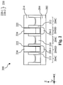
- Fig. 1 illustrates a method 100 for fabricating a semiconductor device from a workpiece 200, fragmentary cross-sectional views of which are illustrated in Figs. 2-13 .
- Method 100 is merely an example and is not intended to limit the present disclosure to what is explicitly illustrated therein. Additional steps can be provided before, during, and after method 100, and some steps described can be replaced, eliminated, or moved around for additional embodiments of the method. Not all steps are described herein in detail for reasons of simplicity.
- the workpiece 200 may include additional transistors, bipolar junction transistors, resistors, capacitors, diodes, fuses, etc., but is simplified for a better understanding of the inventive concepts of the present disclosure.
- like reference numerals denote like features unless otherwise excepted or described. Because a semiconductor device will be fabricated from the workpiece, the workpiece 200 may be referred to as a semiconductor device 200 as the context requires.
- method 100 includes a block 102 where a workpiece 200 is received.
- the workpiece 200 includes an active region 204 over a substrate 202.
- the active region 204 include channel regions 204C and source/drain regions 204SD.
- each of the channel regions 204C may be sandwiched between two source/drain regions 204SD.
- the workpiece 200 further includes gate structures 210 over channel regions 204C and source/drain features 220 over the source/drain regions 204SD.
- a first source/drain feature 220-1 and a second source/drain feature 220-2 are shown in Fig. 2 .
- the first source/drain feature 220-1 and the second source/drain feature 220-2 may be collectively referred to as source/drain features 220.
- Sidewalls of each of the gate structures 210 are lined with gate spacers 212.
- Each of the gate structures 210 and the gate spacers 212 sandwiching it are capped by a gate self-aligned contact (SAC) dielectric feature 214.
- the gate SAC dielectric features 214 are disposed on top surfaces of the gate spacers 212 and the gate structures 210.
- the active region 204 may be a semiconductor fin of a FinFET or may include a vertical stack of nanostructures of an MBC transistor.
- the gate structure 210 may be disposed over the semiconductor fin and be in contact with three sides of the semiconductor fin. When the active region 204 includes a vertical stack of nanostructures, the gate structure 210 may wrap around each of the nanostructures.
- the workpiece 200 further includes a contact etch stop layer (CESL) 222 over the source/drain features 220 and an interlayer dielectric (ILD) layer 224. As shown in Fig. 2 , the CESL 222 is in contact with the source/drain features 220, the gate spacers 212, and the gate SAC dielectric features 214. The ILD layer 224 is separated from the source/drain features 220, the gate spacers 212, and the gate SAC dielectric features 214 by the CESL 222.
- CESL contact etch stop layer
- ILD interlayer dielectric
- the substrate 202 may be a semiconductor substrate such as a silicon substrate.
- the substrate 202 may include various layers, including conductive or insulating layers formed on a semiconductor substrate.
- the substrate 202 may include various doping configurations depending on design requirements as is known in the art.
- the substrate 202 may also include other semiconductors such as germanium (Ge), silicon carbide (SiC), silicon germanium (SiGe), or diamond.
- the substrate 202 may include a compound semiconductor and/or an alloy semiconductor.
- the substrate 202 may include an epitaxial layer (epi-layer), the substrate 202 may be strained for performance enhancement, the substrate 202 may include a silicon-on-insulator (SOI) structure, and/or the substrate 202 may have other suitable enhancement features.
- epi-layer epitaxial layer
- SOI silicon-on-insulator
- the active region 204 may include silicon (Si) or another elementary semiconductor, such as germanium (Ge); a compound semiconductor such as silicon carbide (SiC), gallium arsenide (GaAs), gallium phosphide (GaP), indium phosphide (InP), indium arsenide (InAs), and/or indium antimonide (InSb); an alloy semiconductor such as silicon germanium (SiGe), gallium arsenic phosphorus (GaAsP), aluminum indium arsenic (AlInAs), aluminum gallium arsenic (AlGaAs), indium gallium arsenic (InGaAs), gallium indium phosphorus (GaInP), and/or gallium indium arsenic phosphorus (GaInAsP); or combinations thereof.
- Si silicon germanium
- GaAs gallium arsenic phosphorus
- AlInAs aluminum indium arsenic
- AlGaAs aluminum gallium
- the active region 204 extend lengthwise along the X direction.
- the active region 204 may be fabricated using suitable processes including photolithography and etch processes.
- the photolithography process may include forming a photoresist layer overlying the substrate 202, exposing the photoresist layer to radiation reflected from or transmitting through a photomask, performing post-exposure bake processes, and developing the photoresist layer to form a masking element including the photoresist layer.
- patterning the photoresist layer to form the masking element may be performed using an electron beam (e-beam) lithography process.
- e-beam electron beam
- the masking element may then be used to protect regions of the substrate 202 while an etch process forms recesses into the substrate 202, thereby forming the active region 204.
- the recesses may be etched using a dry etch (e.g., chemical oxide removal), a wet etch, and/or other suitable processes. Numerous other embodiments of methods to form the active region 204 on the substrate 202 may also be used.
- first semiconductor layers and second semiconductors layer are first alternatingly and epitaxially deposited on the substrate 202 to form a layer stack.
- the first semiconductor layer and the second semiconductor layer have different compositions.
- the first semiconductor layer may include silicon (Si) and the second semiconductor layer may include silicon germanium (SiGe).
- the layer stack having first semiconductor nanostructures and second semiconductor nanostructures is then patterned to form fin-shaped structure.
- the second semiconductor layers in the channel regions of fin-shaped structure are then selectively removed to release the first semiconductor layers into suspended nanostructures.
- Gate structures 210 are disposed over channel regions 204C of the active region 204. As illustrated in Fig. 2 , the gate structures 210 extend lengthwise along Y direction, which is perpendicular to the X direction. While not shown in Fig. 2 , each of the gate structures 210 includes an interfacial layer, a gate dielectric layer, one or more work function layers, and a metal fill layer. In some embodiments, the interfacial layer may include a dielectric material such as silicon oxide or silicon hafnium oxide.
- the gate dielectric layer is formed of a high-k (i.e., dielectric constant greater than about 3.9) dielectric material that may include hafnium oxide (HfO), titanium oxide (TiO 2 ), hafnium zirconium oxide (HfZrO), tantalum oxide (Ta 2 O 5 ), hafnium silicon oxide (HfSiO 4 ), zirconium oxide (ZrO 2 ), zirconium silicon oxide (ZrSiO 2 ), lanthanum oxide (La 2 O 3 ), aluminum oxide (Al 2 O 3 ), zirconium oxide (ZrO), yttrium oxide (Y 2 O 3 ), SrTiO 3 (STO), BaTiO 3 (BTO), BaZrO, hafnium lanthanum oxide (HfLaO), lanthanum silicon oxide (LaSiO), aluminum silicon oxide (AlSiO), hafnium tantalum oxide (HfTaO), hafnium titanium oxide (HfT
- the one or more work function layers may include n-type work function layers and p-type work function layers.
- Example n-type work function layers may be formed of aluminum, titanium aluminide, titanium aluminum carbide, tantalum silicon carbide, tantalum silicon aluminum, tantalum silicon carbide, tantalum silicide, or hafnium carbide.
- Example p-type work function layers may be formed of titanium nitride, titanium silicon nitride, tantalum nitride, tungsten carbonitride, or molybdenum.
- the metal fill layer may be formed of a metal, such as tungsten (W), ruthenium (Ru), cobalt (Co), nickel (Ni), or copper (Cu). Because the gate dielectric layer is formed of high-k dielectric material and the use of metal in gate structures 210, gate structures 210 may also be referred to high-k metal gate structures 210 or metal gate structures 210.
- the gate spacer 212 may be a single layer or a multi-layer.
- Example materials for the gate spacer 212 include silicon oxide, silicon nitride, silicon carbide, silicon oxynitride, silicon carbonitride, silicon oxycarbide, silicon oxycarbonitride, and/or combinations thereof.
- the material for the gate spacer 212 is selected such that the gate spacer 212 and the ILD layer 224 have different etching selectivity. That is, the selection of materials allows each of the gate spacer 212 or the ILD layer 224 to be selectively etched without substantially damaging the other.
- the gate spacer 212 is formed of silicon nitride.
- the source/drain features 220 may be epitaxially grown over the source/drain regions 204SD of the active region 204. Depending on the device types and design requirements, the source/drain features 220 may be n-type or p-type.
- n-type source/drain features 220 may include silicon (Si) doped with an n-type dopant, such as phosphorous (P) or arsenic (As) and p-type source/drain features 220 may include silicon germanium (SiGe) doped with a p-type dopant, such as boron (B).
- the source/drain features 220 include a first source/drain feature 220-1 and a second source/drain feature 220-2, which are disposed on different sides of the channel region 204C.
- the ILD layer 224 may be a silicon oxide or silicon oxide containing material where silicon exists in various suitable forms.
- the ILD layer 224 includes silicon oxide or a low-k dielectric material whose k-value (dielectric constant) is smaller than that of silicon oxide, which is about 3.9.
- the low-k dielectric material includes a porous organosilicate thin film such as SiOCH, tetraethylorthosilicate (TEOS) oxide, un-doped silicate glass, doped silicon oxide such as borophosphosilicate glass (BPSG), fused silica glass (FSG), phosphosilicate glass (PSG), fluorine-doped silicon dioxide, carbon-doped silicon dioxide, porous silicon dioxide, porous carbon-doped silicon dioxide, silicon carbon nitride (SiCN), silicon oxycarbide (SiOCN), spin-on silicon based polymeric dielectrics, or combinations thereof.
- a porous organosilicate thin film such as SiOCH, tetraethylorthosilicate (TEOS) oxide, un-doped silicate glass, doped silicon oxide such as borophosphosilicate glass (BPSG), fused silica glass (FSG), phosphosilicate glass (PSG), fluorine-doped silicon dioxide
- the gate SAC dielectric features 214 may be formed of silicon oxide, hafnium silicide, silicon oxycarbide, aluminum oxide, zirconium silicide, aluminum oxynitride, zirconium oxide, hafnium oxide, titanium oxide, zirconium aluminum oxide, zinc oxide, tantalum oxide, lanthanum oxide, yittrium oxide, tantalum carbonitride, silicon nitride, silicon oxycarbonitride, silicon, zirconium nitride, or silicon carbonitride.
- the gate SAC dielectric features 214 is formed of silicon nitride.
- the gate SAC dielectric features 214 may be referred to as a gate capping layer 214.
- a liner may be deposited over the gate structures 210 and the gate spacers 212 before the deposition of the gate SAC dielectric feature 214.
- the liner may include silicon oxide, hafnium silicide, silicon oxycarbide, aluminum oxide, zirconium silicide, aluminum oxynitride, zirconium oxide, hafnium oxide, hafnium zirconium oxide, titanium oxide, zirconium aluminum oxide, zinc oxide, tantalum oxide, lanthanum oxide, yittrium oxide, tantalum carbonitride, silicon nitride, silicon oxycarbonitride, silicon, zirconium nitride, or silicon carbonitride.
- the gate SAC dielectric features 214 and the liner have different compositions such that the gate SAC dielectric features 214 may be selectively etched without substantially etching the liner.
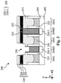
- method 100 includes a block 104 where a contact cut opening 236 is formed over the first source/drain feature 220-1.
- the formation of the contact cut opening 236 may include photolithography processes and etch processes.
- a first resist layer 228 may be deposited over the workpiece 200.
- the first resist layer 228 may be a single layer or a multi-layer.
- the first resist layer 228 is a tri-layer and may include a bottom layer 230, a middle layer 232 over the bottom layer 230, and a top layer 234 over the middle layer 232.
- the bottom layer 230 may be a carbon-rich polymer layer that includes carbon (C), hydrogen (H) and oxygen
- the middle layer may be a silicon-rich polymer layer including silicon (Si), carbon (C), hydrogen (H), and oxygen (O)
- the top layer may be photosensitive polymer layer that includes carbon(C), hydrogen (H) and oxygen (O), and a photosensitive component.
- the top layer 234 is first exposed to a radiation reflected from or transmitting through a photomask, baked in a post-exposure bake process, developed in a development process, and rinsed. The pattern of the photomask is thereby transferred to the top layer 234.
- the patterned top layer 234 is used as an etch mask during the etching the middle layer 232 and the patterned middle layer 232 is used as an etch mask for the patterning of the bottom layer 230.
- the patterned first resist layer 228 includes an opening over the first source/drain feature 220-1.
- the gate SAC dielectric feature 214, the gate spacer 212, the CESL 222, and the ILD layer 224 exposed in the opening are then recessed using the patterned first resist layer 228 as an etch mask to form the contact cut opening 236 over the first source/drain feature 220-1.
- the recessing at block 104 may be a dry etch process.
- the dry etch process may implement an oxygen-containing gas, hydrogen, a fluorine-containing gas (e.g., CF 4 , SF 6 , CH 2 F 2 , CHF 3 , CH 3 F, C 4 H 8 , C 4 F 6 , and/or C 2 F 6 ), a carbon-containing gas (e.g., CO, CH4, and/or C 3 H 8 ), a chlorine-containing gas (e.g., Cl 2 , CHCl 3 , CCl 4 , and/or BCl 3 ), a bromine-containing gas (e.g., HBr and/or CHBR 3 ), an iodine-containing gas, other suitable gases and/or plasmas, and/or combinations thereof.
- a fluorine-containing gas e.g., CF 4 , SF 6 , CH 2 F 2 , CHF 3 , CH 3 F, C 4 H 8 , C 4 F 6 , and/or C 2 F 6
- a carbon-containing gas
- the contact cut opening 236 reduces the height of the ILD layer 224 over the first source/drain feature 220-1 and creates space defined by a top surface of the ILD layer 224 and sidewalls of the CESL 222. In some embodiments represented in Fig. 3 , the contact cut opening 236 does not taper between the CESL 222 over the top surface of the ILD layer 224. In other embodiments illustrated in Figs. 12 and 13 (to be described below), the contact cut opening 236 may taper toward the substrate 202 and may extend partially into the ILD layer 224 or may extend all the way through the depth of the ILD layer 224. Although not explicitly shown in Fig. 3 , the first resist layer 228 is removed by ashing or a suitable method after the formation of the contact cut opening 236.
- method 100 includes a block 106 where a hard mask layer 238 is deposited over the workpiece 200.
- the hard mask layer 238 is deposited into the contact cut opening 236 and is in contact with the top surface of the CESL 222 and the ILD layer 224 over the first source/drain feature 220-1.
- the composition of the hard mask layer 238 may be different from the composition of the ILD layer 224 such that the ILD layer 224 may be selectively etched.
- the hard mask layer 238 may include silicon nitride, silicon, silicon carbide, silicon oxycarbonitride, or silicon carbonitride while the ILD layer 224 may be formed of silicon oxide.
- the hard mask layer 238 includes silicon nitride.
- the hard mask layer 238 may be deposited using atomic layer deposition (ALD), high density plasma chemical vapor deposition (HDPCVD), plasma-enhanced CVD (PECVD), plasma-enhanced ALD (PEALD), or a suitable deposition method that has good hole filling capability.
- ALD atomic layer deposition
- HDPCVD high density plasma chemical vapor deposition
- PECVD plasma-enhanced CVD
- PEALD plasma-enhanced ALD
- the hard mask layer 238 is disposed on the gate SAC dielectric features 214, the CESL 222, and the ILD layer 224.
- the hard mask layer 238 is formed to have a minimum thickness from the top surface of the gate SAC dielectric feature 214. In some instances, the minimum thickness may be between about 10 nm and about 25 nm. The minimum thickness allows improved control of the following planarization process.
- method 100 includes a block 108 where the workpiece 200 is planarized.
- the hard mask layer 238 deposited at block 106 is pulled back by a planarization process, such as a chemical mechanical polishing (CMP) process.
- CMP chemical mechanical polishing
- the hard mask layer 238 over the gate SAC dielectric features 214 and the second source/drain feature 220-2 is removed.
- top surfaces of the gate SAC dielectric features 214, the top surface of the hard mask layer 238 over the first source/drain feature 220-1, the top surface of the ILD layer 224 over the second source/drain feature 220-2, the top surface of the CESL 222 over the second source/drain feature 220-2 are coplanar.
- FIG. 2 there is no etch selectivity between the ILD layer 224 over the first source/drain feature 220-1 and the ILD layer 224 over the second source/drain feature 220-2.
- the hard mask layer 238 allows selective etching of the ILD layer 224 over the second source/drain feature 220-2.
- method 100 includes a block 110 where a dielectric layer 242 and a capping layer 244 are deposited over the workpiece 200.
- a composition of the dielectric layer 242 may be similar to that of the ILD layer 224.
- the dielectric layer 242 may include a porous organosilicate thin film such as SiOCH, tetraethylorthosilicate (TEOS) oxide, un-doped silicate glass, doped silicon oxide such as borophosphosilicate glass (BPSG), fused silica glass (FSG), phosphosilicate glass (PSG), fluorine-doped silicon dioxide, carbon-doped silicon dioxide, porous silicon dioxide, porous carbon-doped silicon dioxide, silicon carbon nitride (SiCN), silicon oxycarbide (SiOCN), spin-on silicon based polymeric dielectrics, or combinations thereof.
- a porous organosilicate thin film such as SiOCH, tetraethylorthosilicate (TEOS) oxide, un-doped silicate glass, doped silicon oxide such as borophosphosilicate glass (BPSG), fused silica glass (FSG), phosphosilicate glass (PSG), fluorine-doped silicon dioxide
- the capping layer 244 may include tungsten carbide, aluminum oxide, zirconium oxide, zinc oxide, titanium oxide, tantalum oxide, hafnium oxide, or a suitable material. In one embodiment, the capping layer 244 includes tungsten carbide. In some embodiments, the dielectric layer 242 may be deposited using spin-on coating or CVD and the capping layer 244 may be deposited using ALD or CVD.
- method 100 includes a block 112 where an access opening 252 through the capping layer 244 are formed. Like operations at block 104, operations at block 112 may include photolithography and etch processes.
- a second resist layer 245 is deposited on the capping layer 244 over the workpiece 200. As shown in Fig. 7 , the second resist layer 245 is a tri-layer and includes a bottom layer 246, a middle layer 248 over the bottom layer 246, and a top layer 250 over the middle layer 248.
- compositions of the bottom layer 246, the middle layer 248, and the top layer 250 are similar to those of the bottom layer 230, the middle layer 232, and the top layer 234 in the first resist layer 228 described above and will not be repeated here.
- the workpiece 200 is etched using the patterned second resist layer 245 as an etch mask to form the access opening 252.
- the access opening 252 extends through the capping layer 244 and partially into the dielectric layer 242.
- the etch process for forming the access opening 252 may include an oxygen-containing gas, hydrogen, a fluorine-containing gas (e.g., CF 4 , SF 6 , CH 2 F 2 , CHF 3 , and/or C 2 F 6 ), a chlorine-containing gas (e.g., Cl 2 , CHCl 3 , CCl 4 , and/or BCl 3 ), a bromine-containing gas (e.g., HBr and/or CHBR 3 ), an iodine-containing gas, other suitable gases and/or plasmas, and/or combinations thereof.
- the access opening 252 spans over both the first source/drain feature 220-1 and the second source/drain feature 220-2.
- the second resist layer 245 is removed by ashing or a suitable method after the formation of the access opening 252.
- method 100 includes a block 114 where a source/drain contact opening 254 to the second source/drain feature 220-2 is formed.
- the CESL 222 and the ILD layer 224 over the second source/drain feature 220-2 are removed in a self-aligned manner to form the source/drain contact opening 254.
- the etch selectivity of the ILD layer 224 relative to the capping layer 244 (shown in Fig. 7 ), the hard mask layer 238, and the gate SAC dielectric feature 214 may be performed using an anisotropic dry etch process.
- Example dry etch process may include an oxygen-containing gas, hydrogen, a fluorine-containing gas (e.g., CF 4 , SF 6 , CH 2 F 2 , CHF 3 , CH 3 F, C 4 H 8 , C 4 F 6 , and/or C 2 F 6 ), a carbon-containing gas (e.g., CO, CH 4 , and/or C 3 H 8 ), a chlorine-containing gas (e.g., Cl 2 , CHCl 3 , CCl 4 , and/or BCl 3 ), a bromine-containing gas ( e.g., HBr and/or CHBR 3 ), an iodine-containing gas, other suitable gases and/or plasmas, and/or combinations thereof.
- the anisotropic dry etch also removes the CESL 222 over the second source/drain feature 220-2 to expose the second source/drain feature 220-2.
- method 100 includes a block 116 where a metal liner 256 is deposited over the workpiece 200.
- the metal liner 256 may include nickel (Ni), cobalt (Co), tantalum (Ta), or titanium (Ti) and may serve as a silicide precursor.
- Ni nickel
- Co cobalt
- Ta tantalum
- Ti titanium
- the workpiece 200 is then annealed to bring about silicidation reaction between silicon in the second source/drain feature 220-2 and the metal liner 256.
- the silicidation reaction results in a silicide feature 257 at the interface between the metal liner 256 and the second source/drain feature 220-2.
- the silicide feature 257 may include nickel silicide, cobalt silicide, tantalum silicide, or titanium silicide.
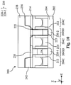
- the silicide feature 257 may reduce the contact resistance between the second source/drain feature 220-2 and a metal fill layer 258 (shown in Fig. 10 ) to be deposited over the silicide feature 257.
- the metal liner 256 is formed of titanium and the silicide feature 257 is formed of titanium silicide.
- the metal liner 256 may be deposited using PVD or a suitable deposition method.
- method 100 includes a block 118 where a metal fill layer 258 is deposited over the workpiece 200.
- the metal fill layer 258 may include tungsten (W), ruthenium (Ru), cobalt (Co), copper (Cu), titanium (Ti), titanium nitride (TiN), tantalum (Ta), tantalum nitride (TaN), molybdenum (Mo), or nickel (Ni) and may be deposited using PVD or a suitable deposition method.
- the metal fill layer 258 is blanketly deposited over the workpiece 200, including in the source/drain contact opening 254 (shown in Fig. 9 ).
- method 100 includes a block 120 where further processes are performed. Such further processes may include planarization of the workpiece 200, formation of gate contacts, and formation of an interconnect structure over the workpiece 200.
- Fig. 11 illustrates the planarization of the workpiece 200 after the deposition of the metal fill layer 258.
- the planarization may include use of a CMP process. As shown in Fig. 11 , the planarization is performed until top surfaces of the gate SAC dielectric features 214, the hard mask layer 238, the metal liner 256, and the metal fill layer 258 are coplanar. At the conclusion of the planarization, a first source/drain contact 260 is substantially formed.
- the first source/drain contact 260 is coupled to the second source/drain feature 220-2.
- the remaining hard mask layer 238 directly over the ILD layer 224 over the first source/drain feature 220-1 may be referred to as the hard mask feature 238.
- the hard mask feature 238 and the ILD layer 224 directly below it may be collectively regarded as a first contact cut feature 270.
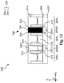
- Figs. 12 and 13 illustrate alternative embodiments of the structures shown in Fig. 11 .
- the contact cut opening 236 shown in Fig. 3 may taper toward the first source/drain feature 220-1 and may extend all the way through the ILD layer 224 over the first source/drain feature 220-1.
- the semiconductor device 200 includes a first tapering hard mask feature 238' that tapers toward the first source/drain feature 220-1.
- the semiconductor device 200 includes a second tapering hard mask feature 238" that tapers toward the first source/drain feature 220-1 and extends all the way through the depth of the ILD layer 224 over the first source/drain feature 220-1.
- the first tapering hard mask feature 238' and the second tapering hard mask feature 238" do not completely displace the ILD layer 224. Instead, a majority portion of them, other than the top portion, are spaced apart from the CESL 222 by the remaining ILD layer 224 along the sidewall of the CESL 222. That is, a portion of the ILD layer 224 may extend between the first tapering hard mask feature 238' and the CESL 222 or between the second tapering hard mask feature 238" and the CESL 222.
- the first contact cut feature 270 may include the first tapering hard mask feature 238' and the ILD layer 224 below it.
- the first contact cut feature 270 may include the second tapering hard mask feature 238" and the surrounding ILD layer 224.
- Fig. 14 is a fragmentary top view of the workpiece 200 shown in Fig. 11 , 12 , or 13 .
- Fig. 14 illustrates a cross-section I-I', which coincides with the cross-sectional planes illustrated in Figs. 11 , 12 and 13 . From left to right, the cross-section I-I' cuts across the gate SAC dielectric feature 214, the first contact cut feature 270, another gate SAC dielectric feature 214, and the first source/drain contact 260. In some embodiments represented in Fig. 14 , the first contact cut feature 270 is aligned with a second source/drain contact 262 along the Y direction.
- the hard mask feature 238 (or the first tapering hard mask feature 238' in Fig.
- the hard mask feature 238 (or the first tapering hard mask feature 238' in Fig. 12 , or the second tapering hard mask feature 238" in Fig. 13 ) protects the underlying ILD layer 224 when the source/drain contact openings for the first source/drain contact 260 and the second source/drain contact 262 are etched.
- the hard mask feature 238 (or the first tapering hard mask feature 238' in Fig. 12 , or the second tapering hard mask feature 238" in Fig. 13 ) prevents the deposition of the metal liner 256 and the metal fill layer 258.
- the hard mask feature 238 (or the first tapering hard mask feature 238' in Fig. 12 , or the second tapering hard mask feature 238" in Fig. 13 ) cuts off the second source/drain contact 262.
- the first source/drain contact 260 is aligned with a second contact cut feature 272 along the Y direction.
- the second contact cut feature 272 cuts short the first source/drain
- embodiments discussed herein offer several advantages over the existing art. It will be understood that not all advantages have been necessarily discussed herein, no particular advantage is required for all embodiments, and other embodiments may offer different advantages.
- embodiments discussed herein include replacing at least a top portion of an ILD layer with a hard mask feature.
- the hard mask feature protects the underlying ILD layer during selective contact opening formation processes. Because the hard mask feature is inlaid into the ILD layer, rather than deposited over the ILD layer, formation of the contact openings does not involve high-aspect-ratio etching. As a result, embodiments of the present disclosure may improve process windows and contact landing areas.
- one of the embodiments of the present disclosure provides a method.
- the method includes receiving a workpiece having a gate structure disposed over a channel region of an active region, a first gate spacer feature disposed along a first sidewall of the gate structure, a second gate spacer feature disposed along a second sidewall of the gate structure, the second sidewall opposing the first sidewall, a gate-top dielectric feature over the gate structure, the first gate spacer feature and the second gate spacer feature, a first source/drain feature disposed over a first source/drain region of the active region, a second source/drain feature disposed over a second source/drain region of the active region, a first dielectric layer over the first source/drain feature, and a second dielectric layer over the second source/drain feature.
- the method further includes forming a contact cut opening over the first source/drain feature while the second dielectric layer is masked, the contact cut opening extending into the first dielectric layer, depositing a hard mask layer over the workpiece, after the depositing of the hard mask layer, planarizing the workpiece to expose the second dielectric layer, forming a source/drain contact opening through the second dielectric layer to expose the second source/drain feature, and forming a source/drain contact in the source/drain contact opening.
- the first dielectric layer and the second dielectric layer include silicon oxide.
- the first gate spacer feature, and the second gate spacer feature, the gate-top dielectric feature, and the hard mask layer include silicon nitride.
- the first source/drain feature underlies the hard mask layer and the first dielectric layer and the second source/drain feature underlies the second dielectric layer.
- the workpiece further includes a contact etch stop layer (CESL) disposed between the first dielectric layer and the first source/drain feature and between the second dielectric layer and the second source/drain feature.
- the channel region of the active region includes a fin-like structure.
- the channel region of the active region includes a vertical stack of nanostructures and the gate structure wraps around each of the vertical stack of nanostructures.
- a composition of the hard mask layer is different from a composition of the second dielectric layer.
- a top surface of the hard mask layer is coplanar with a top surface of the gate-top dielectric feature.
- the forming of the source/drain contact opening includes depositing a top dielectric layer over the workpiece, depositing a tungsten carbide layer over the top dielectric layer, forming an access opening through the tungsten carbide layer, the access opening being over the hard mask layer and the second dielectric layer, and selectively etching the second dielectric layer.
- a method in another of the embodiments, includes receiving a workpiece having a gate structure disposed over a channel region of an active region, a first gate spacer feature disposed along a first sidewall of the gate structure, a second gate spacer feature disposed along a second sidewall of the gate structure, the second sidewall opposing the first sidewall, a gate-top dielectric feature over the gate structure, the first gate spacer feature and the second gate spacer feature, a first source/drain feature disposed over a first source/drain region of the active region, a second source/drain feature disposed over a second source/drain region of the active region, a first dielectric layer over the first source/drain feature, and a second dielectric layer over the second source/drain feature.
- the method further includes replacing a top portion of the first dielectric layer with a hard mask layer, selectively etching the second dielectric layer to form a source/drain contact opening and to expose the second source/drain feature, and after the selectively etching of the second dielectric layer, forming a source/drain contact over the second source/drain feature.
- the first dielectric layer and the second dielectric layer include silicon oxide and the first gate spacer feature, and the second gate spacer feature, the gate-top dielectric feature, and the hard mask layer include silicon nitride.
- the replacing includes forming a contact cut opening over the first source/drain feature while the second dielectric layer is masked, the contact cut opening displacing the top portion of the first dielectric layer, depositing the hard mask layer over the contact cut opening, and planarizing the workpiece until a top surface of the hard mask layer is coplanar with a top surface of the second dielectric layer.
- a composition of the hard mask layer is different from a composition of the second dielectric layer.
- the forming of the source/drain contact includes forming a silicide layer over the workpiece and on the second source/drain feature, depositing a metal fill layer over the silicide layer, and planarizing the workpiece until a top surface of the metal fill layer is coplanar with the top surface of the hard mask layer.
- the selectively etching includes depositing a top dielectric layer over the workpiece, depositing a tungsten carbide layer over the top dielectric layer, forming an access opening through the tungsten carbide layer, the access opening being over the hard mask layer and the second dielectric layer, and selectively etching the second dielectric layer.
- a semiconductor device in yet another of the embodiments, includes a gate structure disposed over a channel region of an active region, a first gate spacer feature disposed along a first sidewall of the gate structure, a second gate spacer feature disposed along a second sidewall of the gate structure, the second sidewall opposing the first sidewall, a gate-top dielectric feature over the gate structure, the first gate spacer feature and the second gate spacer feature, a first source/drain feature disposed over a first source/drain region of the active region, a second source/drain feature disposed over a second source/drain region of the active region, a dielectric layer over the first source/drain feature, a hard mask layer over the dielectric layer, and a source/drain contact over and in contact with the second source/drain feature.
- a top surface of the hard mask layer is coplanar with a top surface of the source/drain contact.
- the dielectric layer includes silicon oxide and the first gate spacer feature, and the second gate spacer feature, the gate-top dielectric feature, and the hard mask layer include silicon nitride.
- the gate-top dielectric feature includes a lower portion and an upper portion over the lower portion, the lower portion is disposed between the dielectric layer and the source/drain contact, and the upper portion is disposed between the hard mask layer and the source/drain contact.
- the channel region of the active region includes a fin-like structure. In some instances, the channel region of the active region includes a vertical stack of nanostructures and the gate structure wraps around each of the vertical stack of nanostructures.
Landscapes
- Insulated Gate Type Field-Effect Transistor (AREA)
- Engineering & Computer Science (AREA)
- Electrodes Of Semiconductors (AREA)
- Chemical & Material Sciences (AREA)
- Crystallography & Structural Chemistry (AREA)
- Nanotechnology (AREA)
- Manufacturing & Machinery (AREA)
- Internal Circuitry In Semiconductor Integrated Circuit Devices (AREA)
- Metal-Oxide And Bipolar Metal-Oxide Semiconductor Integrated Circuits (AREA)
Abstract
A method according to the present disclosure includes receiving a workpiece that includes a gate structure, a first gate spacer feature, a second gate spacer feature, a gate-top dielectric feature over the gate structure, the first gate spacer feature and the second gate spacer feature, a first source/drain feature over a first source/drain region, a second source/drain feature over a second source/drain region, a first dielectric layer over the first source/drain feature, and a second dielectric layer over the second source/drain feature. The method further includes replacing a top portion of the first dielectric layer with a first hard mask layer, forming a second hard mask layer over the first hard mask layer while the second dielectric layer is exposed, etching the second dielectric layer to form a source/drain contact opening and to expose the second source/drain feature, and forming a source/drain contact over the second source/drain feature.
Description
- The electronics industry has experienced an ever-increasing demand for smaller and faster electronic devices which are simultaneously able to support a greater number of increasingly complex and sophisticated functions. Accordingly, there is a continuing trend in the semiconductor industry to manufacture low-cost, high-performance, and low-power integrated circuits (TCs). Thus far these goals have been achieved in large part by scaling down semiconductor IC dimensions (e.g., minimum feature size) and thereby improving production efficiency and lowering associated costs. However, such scaling has also introduced increased complexity to the semiconductor manufacturing process. Thus, the realization of continued advances in semiconductor ICs and devices calls for similar advances in semiconductor manufacturing processes and technology.
- Recently, multi-gate devices, such as fin field-effect transistors (FinFETs) and multi-bridge-channel (MBC) transistors, have been introduced in an effort to improve gate control by increasing gate-channel coupling, reduce OFF-state current, and reduce short-channel effects (SCEs). A FinFET has an elevated channel wrapped by a gate on more than one side (for example, the gate wraps a top and sidewalls of a "fin" of semiconductor material extending from a substrate). An MBC transistor has a gate structure that can extend, partially or fully, around a channel region to provide access to the channel region on two or more sides. Because its gate structure surrounds the channel regions, an MBC transistor may also be referred to as a surrounding gate transistor (SGT) or a gate-all-around (GAA) transistor. The channel region of an MBC transistor may be formed from nanowires, nanosheets, or other nanostructures and for that reasons, an MBC transistor may also be referred to as a nanowire transistor or a nanosheet transistor.
- The three-dimensional structure of the multi-gate devices, allows them to be aggressively scaled while maintaining gate control and mitigating SCEs. Aggressive scaling down of IC dimensions has resulted in densely spaced source/drain features. Formation of source/drain contact openings to these densely packed source/drain features demands high overlay precisions and high-aspect-ratio etching, which may reduce process windows and may increase contact resistance to the source/drain features. Thus, although existing techniques are generally adequate for their intended purposes, they are not entirely satisfactory in all respects.
- Aspects of the present disclosure are best understood from the following detailed description when read with the accompanying figures. It is noted that, in accordance with the standard practice in the industry, various features are not drawn to scale. In fact, the dimensions of the various features may be arbitrarily increased or reduced for clarity of discussion.
-
Fig. 1 is a flowchart of a method forming a gate contact in a semiconductor device, according to one or more aspects of the present disclosure. -
Figs. 2-13 are fragmentary cross-sectional views of a workpiece at various stages of fabrication according to the method inFig. 1 , according to one or more aspects of the present disclosure. -
Fig. 14 is a fragmentary top view of the workpiece inFig. 11 ,12 , or13 , according to one or more aspects of the present disclosure. - The following disclosure provides many different embodiments, or examples, for implementing different features of the provided subject matter. Specific examples of components and arrangements are described below to simplify the present disclosure. These are, of course, merely examples and are not intended to be limiting. For example, the formation of a first feature over or on a second feature in the description that follows may include embodiments in which the first and second features are formed in direct contact, and may also include embodiments in which additional features may be formed between the first and second features, such that the first and second features may not be in direct contact. In addition, the present disclosure may repeat reference numerals and/or letters in the various examples. This repetition is for the purpose of simplicity and clarity and does not in itself dictate a relationship between the various embodiments and/or configurations discussed.
- Further, spatially relative terms, such as "beneath," "below," "lower," "above," "upper" and the like, may be used herein for ease of description to describe one element or feature's relationship to another element(s) or feature(s) as illustrated in the figures. The spatially relative terms are intended to encompass different orientations of the device in use or operation in addition to the orientation depicted in the figures. The apparatus may be otherwise oriented (rotated 90 degrees or at other orientations) and the spatially relative descriptors used herein may likewise be interpreted accordingly.
- Still further, when a number or a range of numbers is described with "about," "approximate," and the like, the term is intended to encompass numbers that are within a reasonable range including the number described, such as within +/- 10% of the number described or other values as understood by person skilled in the art. For example, the term "about 5 nm" encompasses the dimension range from 4.5 nm to 5.5 nm.
- This application relates to semiconductor device structures and methods of forming the same. Particularly, this application relates to self-aligned contact structures and methods.
- A contact cut feature refers to a dielectric feature that separates an otherwise elongated contact structure into multiple segments. For example, an elongated source/drain contact may be separated by one or more source/drain contact cut features into multiple segments, each of which is electrically coupled to one or more of underlying source/drain features of multi-gate devices. In some conventional technologies, the source/drain contact cut feature is formed of the interlayer dielectric (ILD) layer. To retain the source/drain contact cut feature, the hard mask for forming the source/drain contact opening needs to cover and protect the source/drain contact cut feature. As a result, formation of the contact opening involves high-aspect-ratio etching that may reduce process tolerance. Additionally, because the source/drain contact opening may taper towards the source/drain feature from and have smaller cross-sectional area as the opening progresses downward, high aspect ratios may result in smaller landing area and increased contact resistance.
- The present disclosure provides a method to replace at least a top portion of the source/drain contact cut feature with a hard mask layer. The different dielectric material allows selective etching the ILD layer when forming source/drain contact openings. Because the hard mask layer is inlaid into the ILD layer rather than over its top surface, formation of the source/drain contact opening does not require high-aspect-ratio etching and the resultant source/drain contact has an improved landing area.
- The various aspects of the present disclosure will now be described in more detail with reference to the figures. Specifically,
Fig. 1 illustrates amethod 100 for fabricating a semiconductor device from aworkpiece 200, fragmentary cross-sectional views of which are illustrated inFigs. 2-13 .Method 100 is merely an example and is not intended to limit the present disclosure to what is explicitly illustrated therein. Additional steps can be provided before, during, and aftermethod 100, and some steps described can be replaced, eliminated, or moved around for additional embodiments of the method. Not all steps are described herein in detail for reasons of simplicity. Besides what are explicitly shown in figures of the present disclosure, theworkpiece 200 may include additional transistors, bipolar junction transistors, resistors, capacitors, diodes, fuses, etc., but is simplified for a better understanding of the inventive concepts of the present disclosure. Throughout the present disclosure, like reference numerals denote like features unless otherwise excepted or described. Because a semiconductor device will be fabricated from the workpiece, theworkpiece 200 may be referred to as asemiconductor device 200 as the context requires. - Referring to
Figs. 1 and2 ,method 100 includes ablock 102 where aworkpiece 200 is received. As shown inFig. 2 , theworkpiece 200 includes anactive region 204 over asubstrate 202. Theactive region 204 includechannel regions 204C and source/drain regions 204SD. As shown inFig. 2 , each of thechannel regions 204C may be sandwiched between two source/drain regions 204SD. Theworkpiece 200 further includesgate structures 210 overchannel regions 204C and source/drain features 220 over the source/drain regions 204SD. Here, a first source/drain feature 220-1 and a second source/drain feature 220-2 are shown inFig. 2 . For ease of reference, the first source/drain feature 220-1 and the second source/drain feature 220-2 may be collectively referred to as source/drain features 220. Sidewalls of each of thegate structures 210 are lined withgate spacers 212. Each of thegate structures 210 and thegate spacers 212 sandwiching it are capped by a gate self-aligned contact (SAC)dielectric feature 214. As shown inFig. 2 , the gate SACdielectric features 214 are disposed on top surfaces of thegate spacers 212 and thegate structures 210. In some embodiments, theactive region 204 may be a semiconductor fin of a FinFET or may include a vertical stack of nanostructures of an MBC transistor. When theactive region 204 is a semiconductor fin, thegate structure 210 may be disposed over the semiconductor fin and be in contact with three sides of the semiconductor fin. When theactive region 204 includes a vertical stack of nanostructures, thegate structure 210 may wrap around each of the nanostructures. Theworkpiece 200 further includes a contact etch stop layer (CESL) 222 over the source/drain features 220 and an interlayer dielectric (ILD)layer 224. As shown inFig. 2 , theCESL 222 is in contact with the source/drain features 220, thegate spacers 212, and the gate SAC dielectric features 214. TheILD layer 224 is separated from the source/drain features 220, thegate spacers 212, and the gate SAC dielectric features 214 by theCESL 222. - The
substrate 202 may be a semiconductor substrate such as a silicon substrate. Thesubstrate 202 may include various layers, including conductive or insulating layers formed on a semiconductor substrate. Thesubstrate 202 may include various doping configurations depending on design requirements as is known in the art. Thesubstrate 202 may also include other semiconductors such as germanium (Ge), silicon carbide (SiC), silicon germanium (SiGe), or diamond. Alternatively, thesubstrate 202 may include a compound semiconductor and/or an alloy semiconductor. Further, in some embodiments, thesubstrate 202 may include an epitaxial layer (epi-layer), thesubstrate 202 may be strained for performance enhancement, thesubstrate 202 may include a silicon-on-insulator (SOI) structure, and/or thesubstrate 202 may have other suitable enhancement features. - The
active region 204 may include silicon (Si) or another elementary semiconductor, such as germanium (Ge); a compound semiconductor such as silicon carbide (SiC), gallium arsenide (GaAs), gallium phosphide (GaP), indium phosphide (InP), indium arsenide (InAs), and/or indium antimonide (InSb); an alloy semiconductor such as silicon germanium (SiGe), gallium arsenic phosphorus (GaAsP), aluminum indium arsenic (AlInAs), aluminum gallium arsenic (AlGaAs), indium gallium arsenic (InGaAs), gallium indium phosphorus (GaInP), and/or gallium indium arsenic phosphorus (GaInAsP); or combinations thereof. As shown inFig. 2 , theactive region 204 extend lengthwise along the X direction. Theactive region 204 may be fabricated using suitable processes including photolithography and etch processes. The photolithography process may include forming a photoresist layer overlying thesubstrate 202, exposing the photoresist layer to radiation reflected from or transmitting through a photomask, performing post-exposure bake processes, and developing the photoresist layer to form a masking element including the photoresist layer. In some embodiments, patterning the photoresist layer to form the masking element may be performed using an electron beam (e-beam) lithography process. The masking element may then be used to protect regions of thesubstrate 202 while an etch process forms recesses into thesubstrate 202, thereby forming theactive region 204. The recesses may be etched using a dry etch (e.g., chemical oxide removal), a wet etch, and/or other suitable processes. Numerous other embodiments of methods to form theactive region 204 on thesubstrate 202 may also be used. In embodiments where theactive region 204 are a vertical stack of nanostructures of an MBC transistor, first semiconductor layers and second semiconductors layer are first alternatingly and epitaxially deposited on thesubstrate 202 to form a layer stack. The first semiconductor layer and the second semiconductor layer have different compositions. For example, the first semiconductor layer may include silicon (Si) and the second semiconductor layer may include silicon germanium (SiGe). The layer stack having first semiconductor nanostructures and second semiconductor nanostructures is then patterned to form fin-shaped structure. The second semiconductor layers in the channel regions of fin-shaped structure are then selectively removed to release the first semiconductor layers into suspended nanostructures. -
Gate structures 210 are disposed overchannel regions 204C of theactive region 204. As illustrated inFig. 2 , thegate structures 210 extend lengthwise along Y direction, which is perpendicular to the X direction. While not shown inFig. 2 , each of thegate structures 210 includes an interfacial layer, a gate dielectric layer, one or more work function layers, and a metal fill layer. In some embodiments, the interfacial layer may include a dielectric material such as silicon oxide or silicon hafnium oxide. The gate dielectric layer is formed of a high-k (i.e., dielectric constant greater than about 3.9) dielectric material that may include hafnium oxide (HfO), titanium oxide (TiO2), hafnium zirconium oxide (HfZrO), tantalum oxide (Ta2O5), hafnium silicon oxide (HfSiO4), zirconium oxide (ZrO2), zirconium silicon oxide (ZrSiO2), lanthanum oxide (La2O3), aluminum oxide (Al2O3), zirconium oxide (ZrO), yttrium oxide (Y2O3), SrTiO3 (STO), BaTiO3 (BTO), BaZrO, hafnium lanthanum oxide (HfLaO), lanthanum silicon oxide (LaSiO), aluminum silicon oxide (AlSiO), hafnium tantalum oxide (HfTaO), hafnium titanium oxide (HfTiO), (Ba,Sr)TiO3 (BST), silicon nitride (SiN), silicon oxynitride (SiON), combinations thereof, or other suitable material.. The one or more work function layers may include n-type work function layers and p-type work function layers. Example n-type work function layers may be formed of aluminum, titanium aluminide, titanium aluminum carbide, tantalum silicon carbide, tantalum silicon aluminum, tantalum silicon carbide, tantalum silicide, or hafnium carbide. Example p-type work function layers may be formed of titanium nitride, titanium silicon nitride, tantalum nitride, tungsten carbonitride, or molybdenum. The metal fill layer may be formed of a metal, such as tungsten (W), ruthenium (Ru), cobalt (Co), nickel (Ni), or copper (Cu). Because the gate dielectric layer is formed of high-k dielectric material and the use of metal ingate structures 210,gate structures 210 may also be referred to high-kmetal gate structures 210 ormetal gate structures 210. - In some embodiments, the
gate spacer 212 may be a single layer or a multi-layer. Example materials for thegate spacer 212 include silicon oxide, silicon nitride, silicon carbide, silicon oxynitride, silicon carbonitride, silicon oxycarbide, silicon oxycarbonitride, and/or combinations thereof. The material for thegate spacer 212 is selected such that thegate spacer 212 and theILD layer 224 have different etching selectivity. That is, the selection of materials allows each of thegate spacer 212 or theILD layer 224 to be selectively etched without substantially damaging the other. In one example, thegate spacer 212 is formed of silicon nitride. - The source/drain features 220 may be epitaxially grown over the source/drain regions 204SD of the
active region 204. Depending on the device types and design requirements, the source/drain features 220 may be n-type or p-type. For example, n-type source/drain features 220 may include silicon (Si) doped with an n-type dopant, such as phosphorous (P) or arsenic (As) and p-type source/drain features 220 may include silicon germanium (SiGe) doped with a p-type dopant, such as boron (B). The source/drain features 220 include a first source/drain feature 220-1 and a second source/drain feature 220-2, which are disposed on different sides of thechannel region 204C. - The
ILD layer 224 may be a silicon oxide or silicon oxide containing material where silicon exists in various suitable forms. As an example, theILD layer 224 includes silicon oxide or a low-k dielectric material whose k-value (dielectric constant) is smaller than that of silicon oxide, which is about 3.9. In some embodiments, the low-k dielectric material includes a porous organosilicate thin film such as SiOCH, tetraethylorthosilicate (TEOS) oxide, un-doped silicate glass, doped silicon oxide such as borophosphosilicate glass (BPSG), fused silica glass (FSG), phosphosilicate glass (PSG), fluorine-doped silicon dioxide, carbon-doped silicon dioxide, porous silicon dioxide, porous carbon-doped silicon dioxide, silicon carbon nitride (SiCN), silicon oxycarbide (SiOCN), spin-on silicon based polymeric dielectrics, or combinations thereof. - The gate SAC dielectric features 214 may be formed of silicon oxide, hafnium silicide, silicon oxycarbide, aluminum oxide, zirconium silicide, aluminum oxynitride, zirconium oxide, hafnium oxide, titanium oxide, zirconium aluminum oxide, zinc oxide, tantalum oxide, lanthanum oxide, yittrium oxide, tantalum carbonitride, silicon nitride, silicon oxycarbonitride, silicon, zirconium nitride, or silicon carbonitride. In one embodiment, the gate SAC dielectric features 214 is formed of silicon nitride. In some embodiments, the gate SAC dielectric features 214 may be referred to as a
gate capping layer 214. Although not explicitly shown in the figures, in some embodiments, a liner may be deposited over thegate structures 210 and thegate spacers 212 before the deposition of the gate SACdielectric feature 214. The liner may include silicon oxide, hafnium silicide, silicon oxycarbide, aluminum oxide, zirconium silicide, aluminum oxynitride, zirconium oxide, hafnium oxide, hafnium zirconium oxide, titanium oxide, zirconium aluminum oxide, zinc oxide, tantalum oxide, lanthanum oxide, yittrium oxide, tantalum carbonitride, silicon nitride, silicon oxycarbonitride, silicon, zirconium nitride, or silicon carbonitride. When the liner is formed, the gate SAC dielectric features 214 and the liner have different compositions such that the gate SAC dielectric features 214 may be selectively etched without substantially etching the liner. - Referring to
Figs. 1 and3 ,method 100 includes ablock 104 where a contact cut opening 236 is formed over the first source/drain feature 220-1. In some embodiments, the formation of the contact cutopening 236 may include photolithography processes and etch processes. In some instances, a first resist layer 228 may be deposited over theworkpiece 200. The first resist layer 228 may be a single layer or a multi-layer. In some embodiments represented inFig. 3 , the first resist layer 228 is a tri-layer and may include abottom layer 230, a middle layer 232 over thebottom layer 230, and atop layer 234 over the middle layer 232. In one embodiment, thebottom layer 230 may be a carbon-rich polymer layer that includes carbon (C), hydrogen (H) and oxygen, the middle layer may be a silicon-rich polymer layer including silicon (Si), carbon (C), hydrogen (H), and oxygen (O), and the top layer may be photosensitive polymer layer that includes carbon(C), hydrogen (H) and oxygen (O), and a photosensitive component. To pattern the first resist layer 228, thetop layer 234 is first exposed to a radiation reflected from or transmitting through a photomask, baked in a post-exposure bake process, developed in a development process, and rinsed. The pattern of the photomask is thereby transferred to thetop layer 234. The patternedtop layer 234 is used as an etch mask during the etching the middle layer 232 and the patterned middle layer 232 is used as an etch mask for the patterning of thebottom layer 230. As shown inFig. 3 , the patterned first resist layer 228 includes an opening over the first source/drain feature 220-1. The gate SACdielectric feature 214, thegate spacer 212, theCESL 222, and theILD layer 224 exposed in the opening are then recessed using the patterned first resist layer 228 as an etch mask to form the contact cutopening 236 over the first source/drain feature 220-1. In some embodiments, the recessing atblock 104 may be a dry etch process. For example, the dry etch process may implement an oxygen-containing gas, hydrogen, a fluorine-containing gas (e.g., CF4, SF6, CH2F2, CHF3, CH3F, C4H8, C4F6, and/or C2F6), a carbon-containing gas (e.g., CO, CH4, and/or C3H8), a chlorine-containing gas (e.g., Cl2, CHCl3, CCl4, and/or BCl3), a bromine-containing gas (e.g., HBr and/or CHBR3), an iodine-containing gas, other suitable gases and/or plasmas, and/or combinations thereof. - The contact cut
opening 236 reduces the height of theILD layer 224 over the first source/drain feature 220-1 and creates space defined by a top surface of theILD layer 224 and sidewalls of theCESL 222. In some embodiments represented inFig. 3 , the contact cutopening 236 does not taper between theCESL 222 over the top surface of theILD layer 224. In other embodiments illustrated inFigs. 12 and13 (to be described below), the contact cutopening 236 may taper toward thesubstrate 202 and may extend partially into theILD layer 224 or may extend all the way through the depth of theILD layer 224. Although not explicitly shown inFig. 3 , the first resist layer 228 is removed by ashing or a suitable method after the formation of the contact cutopening 236. - Referring to
Figs. 1 and4 ,method 100 includes ablock 106 where ahard mask layer 238 is deposited over theworkpiece 200. As shown inFig. 4 , thehard mask layer 238 is deposited into the contact cutopening 236 and is in contact with the top surface of theCESL 222 and theILD layer 224 over the first source/drain feature 220-1. In some embodiments, the composition of thehard mask layer 238 may be different from the composition of theILD layer 224 such that theILD layer 224 may be selectively etched. In some embodiments, thehard mask layer 238 may include silicon nitride, silicon, silicon carbide, silicon oxycarbonitride, or silicon carbonitride while theILD layer 224 may be formed of silicon oxide. In one embodiment, thehard mask layer 238 includes silicon nitride. In some implementations, thehard mask layer 238 may be deposited using atomic layer deposition (ALD), high density plasma chemical vapor deposition (HDPCVD), plasma-enhanced CVD (PECVD), plasma-enhanced ALD (PEALD), or a suitable deposition method that has good hole filling capability. In some embodiments represented inFig. 4 , thehard mask layer 238 is disposed on the gate SAC dielectric features 214, theCESL 222, and theILD layer 224. In some implementations, thehard mask layer 238 is formed to have a minimum thickness from the top surface of the gate SACdielectric feature 214. In some instances, the minimum thickness may be between about 10 nm and about 25 nm. The minimum thickness allows improved control of the following planarization process. - Referring to
Figs. 1 and5 ,method 100 includes ablock 108 where theworkpiece 200 is planarized. Atblock 108, thehard mask layer 238 deposited atblock 106 is pulled back by a planarization process, such as a chemical mechanical polishing (CMP) process. As shown inFig. 5 , thehard mask layer 238 over the gate SAC dielectric features 214 and the second source/drain feature 220-2 is removed. As a result, top surfaces of the gate SAC dielectric features 214, the top surface of thehard mask layer 238 over the first source/drain feature 220-1, the top surface of theILD layer 224 over the second source/drain feature 220-2, the top surface of theCESL 222 over the second source/drain feature 220-2 are coplanar. - Reference is now made to
Figs. 2 and5 . It can be seen that operations atblock ILD layer 224 over the first source/drain feature 220-1 with thehard mask layer 238. That is, instead of depositing a hard mask layer over theILD layer 224, thehard mask layer 238 is inlaid into theILD layer 224. InFig. 2 , there is no etch selectivity between theILD layer 224 over the first source/drain feature 220-1 and theILD layer 224 over the second source/drain feature 220-2. Turning toFig. 5 , while theILD layer 224 over the second source/drain feature 220-2 remains exposed, theILD layer 224 over the first source/drain feature 220-1 is protected by thehard mask layer 238. Because thehard mask layer 238 has a different composition from theILD layer 224, thehard mask layer 238 allow selective etching of theILD layer 224 over the second source/drain feature 220-2. - Referring to
Figs. 1 and6 ,method 100 includes ablock 110 where adielectric layer 242 and acapping layer 244 are deposited over theworkpiece 200. In some embodiments, a composition of thedielectric layer 242 may be similar to that of theILD layer 224. In some instances, thedielectric layer 242 may include a porous organosilicate thin film such as SiOCH, tetraethylorthosilicate (TEOS) oxide, un-doped silicate glass, doped silicon oxide such as borophosphosilicate glass (BPSG), fused silica glass (FSG), phosphosilicate glass (PSG), fluorine-doped silicon dioxide, carbon-doped silicon dioxide, porous silicon dioxide, porous carbon-doped silicon dioxide, silicon carbon nitride (SiCN), silicon oxycarbide (SiOCN), spin-on silicon based polymeric dielectrics, or combinations thereof. Thecapping layer 244 may include tungsten carbide, aluminum oxide, zirconium oxide, zinc oxide, titanium oxide, tantalum oxide, hafnium oxide, or a suitable material. In one embodiment, thecapping layer 244 includes tungsten carbide. In some embodiments, thedielectric layer 242 may be deposited using spin-on coating or CVD and thecapping layer 244 may be deposited using ALD or CVD. - Referring to
Figs. 1 and7 ,method 100 includes a block 112 where an access opening 252 through thecapping layer 244 are formed. Like operations atblock 104, operations at block 112 may include photolithography and etch processes. At block 112, a second resistlayer 245 is deposited on thecapping layer 244 over theworkpiece 200. As shown inFig. 7 , the second resistlayer 245 is a tri-layer and includes abottom layer 246, amiddle layer 248 over thebottom layer 246, and atop layer 250 over themiddle layer 248. The compositions of thebottom layer 246, themiddle layer 248, and thetop layer 250 are similar to those of thebottom layer 230, the middle layer 232, and thetop layer 234 in the first resist layer 228 described above and will not be repeated here. After the second resistlayer 245 is patterned in a fashion similar to the patterning of the first resist layer 228, theworkpiece 200 is etched using the patterned second resistlayer 245 as an etch mask to form theaccess opening 252. Theaccess opening 252 extends through thecapping layer 244 and partially into thedielectric layer 242. The etch process for forming the access opening 252 may include an oxygen-containing gas, hydrogen, a fluorine-containing gas (e.g., CF4, SF6, CH2F2, CHF3, and/or C2F6), a chlorine-containing gas (e.g., Cl2, CHCl3, CCl4, and/or BCl3), a bromine-containing gas (e.g., HBr and/or CHBR3), an iodine-containing gas, other suitable gases and/or plasmas, and/or combinations thereof. Theaccess opening 252 spans over both the first source/drain feature 220-1 and the second source/drain feature 220-2. Although not explicitly shown in the figures, the second resistlayer 245 is removed by ashing or a suitable method after the formation of theaccess opening 252. - Referring to
Figs. 1 and8 ,method 100 includes ablock 114 where a source/drain contact opening 254 to the second source/drain feature 220-2 is formed. Atblock 114, theCESL 222 and theILD layer 224 over the second source/drain feature 220-2 are removed in a self-aligned manner to form the source/drain contact opening 254. such self-alignment is achieved by the etch selectivity of theILD layer 224 relative to the capping layer 244 (shown inFig. 7 ), thehard mask layer 238, and the gate SACdielectric feature 214. In some embodiments, the etching/removal of theILD layer 224 may be performed using an anisotropic dry etch process. Example dry etch process may include an oxygen-containing gas, hydrogen, a fluorine-containing gas (e.g., CF4, SF6, CH2F2, CHF3, CH3F, C4H8, C4F6, and/or C2F6), a carbon-containing gas (e.g., CO, CH4, and/or C3H8), a chlorine-containing gas (e.g., Cl2, CHCl3, CCl4, and/or BCl3), a bromine-containing gas (e.g., HBr and/or CHBR3), an iodine-containing gas, other suitable gases and/or plasmas, and/or combinations thereof. As shown inFig. 8 , the anisotropic dry etch also removes theCESL 222 over the second source/drain feature 220-2 to expose the second source/drain feature 220-2. - Referring to
Figs. 1 and9 ,method 100 includes ablock 116 where ametal liner 256 is deposited over theworkpiece 200. Themetal liner 256 may include nickel (Ni), cobalt (Co), tantalum (Ta), or titanium (Ti) and may serve as a silicide precursor. As themetal liner 256 is deposited over theworkpiece 200, it is disposed on and in contact with the exposed second source/drain feature 220-2. Theworkpiece 200 is then annealed to bring about silicidation reaction between silicon in the second source/drain feature 220-2 and themetal liner 256. The silicidation reaction results in asilicide feature 257 at the interface between themetal liner 256 and the second source/drain feature 220-2. In some instance, thesilicide feature 257 may include nickel silicide, cobalt silicide, tantalum silicide, or titanium silicide. Thesilicide feature 257 may reduce the contact resistance between the second source/drain feature 220-2 and a metal fill layer 258 (shown inFig. 10 ) to be deposited over thesilicide feature 257. In one embodiment, themetal liner 256 is formed of titanium and thesilicide feature 257 is formed of titanium silicide. Themetal liner 256 may be deposited using PVD or a suitable deposition method. - Referring to
Figs. 1 and10 ,method 100 includes ablock 118 where ametal fill layer 258 is deposited over theworkpiece 200. In some embodiment, themetal fill layer 258 may include tungsten (W), ruthenium (Ru), cobalt (Co), copper (Cu), titanium (Ti), titanium nitride (TiN), tantalum (Ta), tantalum nitride (TaN), molybdenum (Mo), or nickel (Ni) and may be deposited using PVD or a suitable deposition method. As shown inFig. 10 , themetal fill layer 258 is blanketly deposited over theworkpiece 200, including in the source/drain contact opening 254 (shown inFig. 9 ). - Referring to
Figs. 1 and11 ,method 100 includes ablock 120 where further processes are performed. Such further processes may include planarization of theworkpiece 200, formation of gate contacts, and formation of an interconnect structure over theworkpiece 200.Fig. 11 illustrates the planarization of theworkpiece 200 after the deposition of themetal fill layer 258. The planarization may include use of a CMP process. As shown inFig. 11 , the planarization is performed until top surfaces of the gate SAC dielectric features 214, thehard mask layer 238, themetal liner 256, and themetal fill layer 258 are coplanar. At the conclusion of the planarization, a first source/drain contact 260 is substantially formed. The first source/drain contact 260 is coupled to the second source/drain feature 220-2. After the planarization atblock 120, the remaininghard mask layer 238 directly over theILD layer 224 over the first source/drain feature 220-1 may be referred to as thehard mask feature 238. The hard mask feature 238 and theILD layer 224 directly below it may be collectively regarded as a first contact cutfeature 270. -
Figs. 12 and13 illustrate alternative embodiments of the structures shown inFig. 11 . In some instances, the contact cutopening 236 shown inFig. 3 may taper toward the first source/drain feature 220-1 and may extend all the way through theILD layer 224 over the first source/drain feature 220-1. In an alternative embodiment shown inFig. 12 , thesemiconductor device 200 includes a first tapering hard mask feature 238' that tapers toward the first source/drain feature 220-1. In another alternative embodiment shown inFig. 13 , thesemiconductor device 200 includes a second tapering hard mask feature 238" that tapers toward the first source/drain feature 220-1 and extends all the way through the depth of theILD layer 224 over the first source/drain feature 220-1. As shown inFigs. 12 and13 , because of the tapering shapes, the first tapering hard mask feature 238' and the second tapering hard mask feature 238" do not completely displace theILD layer 224. Instead, a majority portion of them, other than the top portion, are spaced apart from theCESL 222 by the remainingILD layer 224 along the sidewall of theCESL 222. That is, a portion of theILD layer 224 may extend between the first tapering hard mask feature 238' and theCESL 222 or between the second tapering hard mask feature 238" and theCESL 222. In the alternative embodiment shown inFig. 12 , the first contact cutfeature 270 may include the first tapering hard mask feature 238' and theILD layer 224 below it. In the other alternative embodiment shown inFig. 13 , the first contact cutfeature 270 may include the second tapering hard mask feature 238" and the surroundingILD layer 224. -
Fig. 14 is a fragmentary top view of theworkpiece 200 shown inFig. 11 ,12 , or13 .Fig. 14 illustrates a cross-section I-I', which coincides with the cross-sectional planes illustrated inFigs. 11 ,12 and13 . From left to right, the cross-section I-I' cuts across the gate SACdielectric feature 214, the first contact cutfeature 270, another gate SACdielectric feature 214, and the first source/drain contact 260. In some embodiments represented inFig. 14 , the first contact cutfeature 270 is aligned with a second source/drain contact 262 along the Y direction. The hard mask feature 238 (or the first tapering hard mask feature 238' inFig. 12 , or the second tapering hard mask feature 238" inFig. 13 ) protects theunderlying ILD layer 224 when the source/drain contact openings for the first source/drain contact 260 and the second source/drain contact 262 are etched. Put differently, the hard mask feature 238 (or the first tapering hard mask feature 238' inFig. 12 , or the second tapering hard mask feature 238" inFig. 13 ) prevents the deposition of themetal liner 256 and themetal fill layer 258. As a result, the hard mask feature 238 (or the first tapering hard mask feature 238' inFig. 12 , or the second tapering hard mask feature 238" inFig. 13 ) cuts off the second source/drain contact 262. Similarly, the first source/drain contact 260 is aligned with a second contact cutfeature 272 along the Y direction. The second contact cutfeature 272 cuts short the first source/drain contact 260. - Thus, the various embodiments described herein offer several advantages over the existing art. It will be understood that not all advantages have been necessarily discussed herein, no particular advantage is required for all embodiments, and other embodiments may offer different advantages. For example, embodiments discussed herein include replacing at least a top portion of an ILD layer with a hard mask feature. The hard mask feature protects the underlying ILD layer during selective contact opening formation processes. Because the hard mask feature is inlaid into the ILD layer, rather than deposited over the ILD layer, formation of the contact openings does not involve high-aspect-ratio etching. As a result, embodiments of the present disclosure may improve process windows and contact landing areas.
- Thus, one of the embodiments of the present disclosure provides a method. The method includes receiving a workpiece having a gate structure disposed over a channel region of an active region, a first gate spacer feature disposed along a first sidewall of the gate structure, a second gate spacer feature disposed along a second sidewall of the gate structure, the second sidewall opposing the first sidewall, a gate-top dielectric feature over the gate structure, the first gate spacer feature and the second gate spacer feature, a first source/drain feature disposed over a first source/drain region of the active region, a second source/drain feature disposed over a second source/drain region of the active region, a first dielectric layer over the first source/drain feature, and a second dielectric layer over the second source/drain feature. The method further includes forming a contact cut opening over the first source/drain feature while the second dielectric layer is masked, the contact cut opening extending into the first dielectric layer, depositing a hard mask layer over the workpiece, after the depositing of the hard mask layer, planarizing the workpiece to expose the second dielectric layer, forming a source/drain contact opening through the second dielectric layer to expose the second source/drain feature, and forming a source/drain contact in the source/drain contact opening.
- In some embodiments, the first dielectric layer and the second dielectric layer include silicon oxide. The first gate spacer feature, and the second gate spacer feature, the gate-top dielectric feature, and the hard mask layer include silicon nitride. In some embodiments, after the planarizing of the workpiece, the first source/drain feature underlies the hard mask layer and the first dielectric layer and the second source/drain feature underlies the second dielectric layer. In some implementations, the workpiece further includes a contact etch stop layer (CESL) disposed between the first dielectric layer and the first source/drain feature and between the second dielectric layer and the second source/drain feature. In some embodiments, the channel region of the active region includes a fin-like structure. In some instances, the channel region of the active region includes a vertical stack of nanostructures and the gate structure wraps around each of the vertical stack of nanostructures. In some instances, a composition of the hard mask layer is different from a composition of the second dielectric layer. In some embodiments, after the planarizing of the workpiece, a top surface of the hard mask layer is coplanar with a top surface of the gate-top dielectric feature. In some implementations, the forming of the source/drain contact opening includes depositing a top dielectric layer over the workpiece, depositing a tungsten carbide layer over the top dielectric layer, forming an access opening through the tungsten carbide layer, the access opening being over the hard mask layer and the second dielectric layer, and selectively etching the second dielectric layer.
- In another of the embodiments, a method is provided. The method includes receiving a workpiece having a gate structure disposed over a channel region of an active region, a first gate spacer feature disposed along a first sidewall of the gate structure, a second gate spacer feature disposed along a second sidewall of the gate structure, the second sidewall opposing the first sidewall, a gate-top dielectric feature over the gate structure, the first gate spacer feature and the second gate spacer feature, a first source/drain feature disposed over a first source/drain region of the active region, a second source/drain feature disposed over a second source/drain region of the active region, a first dielectric layer over the first source/drain feature, and a second dielectric layer over the second source/drain feature. The method further includes replacing a top portion of the first dielectric layer with a hard mask layer, selectively etching the second dielectric layer to form a source/drain contact opening and to expose the second source/drain feature, and after the selectively etching of the second dielectric layer, forming a source/drain contact over the second source/drain feature.
- In some embodiments, the first dielectric layer and the second dielectric layer include silicon oxide and the first gate spacer feature, and the second gate spacer feature, the gate-top dielectric feature, and the hard mask layer include silicon nitride. In some implementations, the replacing includes forming a contact cut opening over the first source/drain feature while the second dielectric layer is masked, the contact cut opening displacing the top portion of the first dielectric layer, depositing the hard mask layer over the contact cut opening, and planarizing the workpiece until a top surface of the hard mask layer is coplanar with a top surface of the second dielectric layer. In some implementations, a composition of the hard mask layer is different from a composition of the second dielectric layer. In some instances, the forming of the source/drain contact includes forming a silicide layer over the workpiece and on the second source/drain feature, depositing a metal fill layer over the silicide layer, and planarizing the workpiece until a top surface of the metal fill layer is coplanar with the top surface of the hard mask layer. In some instances, the selectively etching includes depositing a top dielectric layer over the workpiece, depositing a tungsten carbide layer over the top dielectric layer, forming an access opening through the tungsten carbide layer, the access opening being over the hard mask layer and the second dielectric layer, and selectively etching the second dielectric layer.
- In yet another of the embodiments, a semiconductor device is provided. The semiconductor device includes a gate structure disposed over a channel region of an active region, a first gate spacer feature disposed along a first sidewall of the gate structure, a second gate spacer feature disposed along a second sidewall of the gate structure, the second sidewall opposing the first sidewall, a gate-top dielectric feature over the gate structure, the first gate spacer feature and the second gate spacer feature, a first source/drain feature disposed over a first source/drain region of the active region, a second source/drain feature disposed over a second source/drain region of the active region, a dielectric layer over the first source/drain feature, a hard mask layer over the dielectric layer, and a source/drain contact over and in contact with the second source/drain feature. A top surface of the hard mask layer is coplanar with a top surface of the source/drain contact.
- In some embodiments, the dielectric layer includes silicon oxide and the first gate spacer feature, and the second gate spacer feature, the gate-top dielectric feature, and the hard mask layer include silicon nitride. In some embodiments, the gate-top dielectric feature includes a lower portion and an upper portion over the lower portion, the lower portion is disposed between the dielectric layer and the source/drain contact, and the upper portion is disposed between the hard mask layer and the source/drain contact. In some implementations, the channel region of the active region includes a fin-like structure. In some instances, the channel region of the active region includes a vertical stack of nanostructures and the gate structure wraps around each of the vertical stack of nanostructures.
- The foregoing outlines features of several embodiments so that those skilled in the art may better understand the aspects of the present disclosure. Those skilled in the art should appreciate that they may readily use the present disclosure as a basis for designing or modifying other processes and structures for carrying out the same purposes and/or achieving the same advantages of the embodiments introduced herein. Those skilled in the art should also realize that such equivalent constructions do not depart from the spirit and scope of the present disclosure, and that they may make various changes, substitutions, and alterations herein without departing from the spirit and scope of the present disclosure.
Claims (9)
- A method, comprising:receiving a workpiece comprising:a gate structure disposed over a channel region of an active region,a first gate spacer feature disposed along a first sidewall of the gate structure,a second gate spacer feature disposed along a second sidewall of the gate structure, the second sidewall opposing the first sidewall,a gate-top dielectric feature over the gate structure, the first gate spacer feature and the second gate spacer feature,a first source/drain feature disposed over a first source/drain region of the active region,a second source/drain feature disposed over a second source/drain region of the active region,a first dielectric layer over the first source/drain feature, anda second dielectric layer over the second source/drain feature;forming a contact cut opening over the first source/drain feature while the second dielectric layer is masked, the contact cut opening extending into the first dielectric layer;depositing a hard mask layer over the workpiece;after the depositing of the hard mask layer, planarizing the workpiece to expose the second dielectric layer;forming a source/drain contact opening through the second dielectric layer to expose the second source/drain feature; andforming a source/drain contact in the source/drain contact opening.
- The method of claim 1,wherein the first dielectric layer and the second dielectric layer comprise silicon oxide,wherein the first gate spacer feature, and the second gate spacer feature, the gate-top dielectric feature, and the hard mask layer comprise silicon nitride.
- The method of claim 1, wherein, after the planarizing of the workpiece, the first source/drain feature underlies the hard mask layer and the first dielectric layer and the second source/drain feature underlies the second dielectric layer.
- The method of claim 1, wherein the workpiece further comprises a contact etch stop layer (CESL) disposed between the first dielectric layer and the first source/drain feature and between the second dielectric layer and the second source/drain feature.
- The method of claim 1, wherein the channel region of the active region comprises a fin-like structure.
- The method of claim 1, wherein the channel region of the active region comprises a vertical stack of nanostructures and the gate structure wraps around each of the vertical stack of nanostructures.
- The method of claim 1, wherein a composition of the hard mask layer is different from a composition of the second dielectric layer.
- The method of claim 1, wherein, after the planarizing of the workpiece, a top surface of the hard mask layer is coplanar with a top surface of the gate-top dielectric feature.
- The method of claim 1, wherein the forming of the source/drain contact opening comprises:depositing a top dielectric layer over the workpiece;depositing a tungsten carbide layer over the top dielectric layer;forming an access opening through the tungsten carbide layer, the access opening being over the hard mask layer and the second dielectric layer; andselectively etching the second dielectric layer.
Applications Claiming Priority (1)
| Application Number | Priority Date | Filing Date | Title |
|---|---|---|---|
| US16/935,686 US11387331B2 (en) | 2020-07-22 | 2020-07-22 | Source/drain contact structure |
Publications (1)
| Publication Number | Publication Date |
|---|---|
| EP3944296A1 true EP3944296A1 (en) | 2022-01-26 |
Family
ID=77021152
Family Applications (1)
| Application Number | Title | Priority Date | Filing Date |
|---|---|---|---|
| EP21186960.7A Withdrawn EP3944296A1 (en) | 2020-07-22 | 2021-07-21 | Source/drain contact structure |
Country Status (5)
| Country | Link |
|---|---|
| US (3) | US11387331B2 (en) |
| EP (1) | EP3944296A1 (en) |
| JP (1) | JP2022022164A (en) |
| CN (1) | CN113725163A (en) |
| TW (1) | TW202205447A (en) |
Families Citing this family (5)
| Publication number | Priority date | Publication date | Assignee | Title |
|---|---|---|---|---|
| US20230008496A1 (en) * | 2021-07-09 | 2023-01-12 | Taiwan Semiconductor Manufacturing Co., Ltd. | Contact structure for semiconductor device |
| US12494411B2 (en) * | 2022-02-17 | 2025-12-09 | Taiwan Semiconductor Manufacturing Company, Ltd. | Integrated circuit and method of forming the same |
| US20230268403A1 (en) * | 2022-02-22 | 2023-08-24 | Taiwan Semiconductor Manufacturing Co., Ltd. | Semiconductor device having front side and back side source/drain contacts |
| US12588229B2 (en) | 2022-07-08 | 2026-03-24 | Taiwan Semiconductor Manufacturing Company, Ltd. | Gate-top dielectric structure for self-aligned contact |
| US12563776B2 (en) | 2023-04-06 | 2026-02-24 | International Business Machines Corporation | Forming source/drain contact in a tight tip-to-tip space |
Citations (4)
| Publication number | Priority date | Publication date | Assignee | Title |
|---|---|---|---|---|
| US20160071774A1 (en) * | 2014-09-10 | 2016-03-10 | Global Foundries Inc. | Opposite polarity borderless replacement metal contact scheme |
| US20180366324A1 (en) * | 2017-06-19 | 2018-12-20 | Globalfoundries Inc. | Replacement contact cuts with an encapsulated low-k dielectric |
| US20200006139A1 (en) * | 2018-06-27 | 2020-01-02 | Taiwan Semiconductor Manufacturing Co., Ltd. | Semiconductor device with reduced via bridging risk |
| US20200126857A1 (en) * | 2018-10-22 | 2020-04-23 | Taiwan Semiconductor Manufacturing Co., Ltd. | Using Mask Layers to Facilitate the Formation of Self-Aligned Contacts and Vias |
Family Cites Families (9)
| Publication number | Priority date | Publication date | Assignee | Title |
|---|---|---|---|---|
| US9029260B2 (en) | 2011-06-16 | 2015-05-12 | Taiwan Semiconductor Manufacturing Company, Ltd. | Gap filling method for dual damascene process |
| US8779592B2 (en) | 2012-05-01 | 2014-07-15 | Taiwan Semiconductor Manufacturing Company, Ltd. | Via-free interconnect structure with self-aligned metal line interconnections |
| US9613856B1 (en) | 2015-09-18 | 2017-04-04 | Taiwan Semiconductor Manufacturing Company, Ltd. | Method of forming metal interconnection |
| US9972529B2 (en) | 2015-09-28 | 2018-05-15 | Taiwan Semiconductor Manufacturing Company, Ltd. | Method of forming metal interconnection |
| US9768061B1 (en) | 2016-05-31 | 2017-09-19 | Taiwan Semiconductor Manufacturing Co., Ltd. | Low-k dielectric interconnect systems |
| US10355095B2 (en) * | 2017-03-31 | 2019-07-16 | Taiwan Semiconductor Manufacturing Co., Ltd. | FinFET structure with composite gate helmet |
| US10153198B2 (en) * | 2017-04-07 | 2018-12-11 | Taiwan Semiconductor Manufacturing Company, Ltd. | Low-resistance contact plugs and method forming same |
| US10355102B2 (en) * | 2017-11-15 | 2019-07-16 | Taiwan Semiconductor Manufacturing Co., Ltd. | Semiconductor device and method of manufacturing the same |
| US10170322B1 (en) | 2017-11-16 | 2019-01-01 | Taiwan Semiconductor Manufacturing Co., Ltd. | Atomic layer deposition based process for contact barrier layer |
-
2020
- 2020-07-22 US US16/935,686 patent/US11387331B2/en active Active
-
2021
- 2021-06-28 CN CN202110717995.3A patent/CN113725163A/en active Pending
- 2021-07-05 TW TW110124546A patent/TW202205447A/en unknown
- 2021-07-21 EP EP21186960.7A patent/EP3944296A1/en not_active Withdrawn
- 2021-07-21 JP JP2021120148A patent/JP2022022164A/en active Pending
-
2022
- 2022-06-30 US US17/854,817 patent/US12166088B2/en active Active
-
2024
- 2024-12-09 US US18/974,261 patent/US20250107196A1/en active Pending
Patent Citations (4)
| Publication number | Priority date | Publication date | Assignee | Title |
|---|---|---|---|---|
| US20160071774A1 (en) * | 2014-09-10 | 2016-03-10 | Global Foundries Inc. | Opposite polarity borderless replacement metal contact scheme |
| US20180366324A1 (en) * | 2017-06-19 | 2018-12-20 | Globalfoundries Inc. | Replacement contact cuts with an encapsulated low-k dielectric |
| US20200006139A1 (en) * | 2018-06-27 | 2020-01-02 | Taiwan Semiconductor Manufacturing Co., Ltd. | Semiconductor device with reduced via bridging risk |
| US20200126857A1 (en) * | 2018-10-22 | 2020-04-23 | Taiwan Semiconductor Manufacturing Co., Ltd. | Using Mask Layers to Facilitate the Formation of Self-Aligned Contacts and Vias |
Also Published As
| Publication number | Publication date |
|---|---|
| US12166088B2 (en) | 2024-12-10 |
| US20220336592A1 (en) | 2022-10-20 |
| TW202205447A (en) | 2022-02-01 |
| CN113725163A (en) | 2021-11-30 |
| US11387331B2 (en) | 2022-07-12 |
| US20250107196A1 (en) | 2025-03-27 |
| US20220028983A1 (en) | 2022-01-27 |
| JP2022022164A (en) | 2022-02-03 |
Similar Documents
| Publication | Publication Date | Title |
|---|---|---|
| US12166088B2 (en) | Source/drain contact structure | |
| US12191370B2 (en) | Semiconductor device with tunable channel layer usage and methods of fabrication thereof | |
| US12261214B2 (en) | Multi-gate transistor structure | |
| KR102638127B1 (en) | Etch profile control of via opening | |
| US12568670B2 (en) | Self-aligned contact structures | |
| CN113113296A (en) | Method for manufacturing semiconductor device | |
| US12532532B2 (en) | Epitaxial features in semiconductor devices and method of manufacturing | |
| US20240387261A1 (en) | Gate contact structure | |
| US20220115387A1 (en) | Semiconductor device having an offset source/drain feature and method of fabricating thereof | |
| US20260013192A1 (en) | Semiconductor Structures With Reduced Parasitic Capacitance And Methods For Forming The Same | |
| US20260114016A1 (en) | Semiconductor device contact structures and methods of fabricating thereof | |
| TWI807783B (en) | Semiconductor structures and methods for fabricating the same | |
| TWI824371B (en) | Semiconductor device and method of forming the same | |
| US20240421200A1 (en) | Source/Drain Contacts and Methods for Forming the Same | |
| US20250374652A1 (en) | Semiconductor structures with reduced parasitic capacitance | |
| US20250351478A1 (en) | Hybrid nanostructure scheme and methods for forming the same | |
| US20260114042A1 (en) | Channel strain engineering for semiconductor devices | |
| US20260026052A1 (en) | Semiconductor structures and methods of forming the same | |
| US20250386545A1 (en) | Method of forming backside vias |
Legal Events
| Date | Code | Title | Description |
|---|---|---|---|
| PUAI | Public reference made under article 153(3) epc to a published international application that has entered the european phase |
Free format text: ORIGINAL CODE: 0009012 |
|
| STAA | Information on the status of an ep patent application or granted ep patent |
Free format text: STATUS: THE APPLICATION HAS BEEN PUBLISHED |
|
| AK | Designated contracting states |
Kind code of ref document: A1 Designated state(s): AL AT BE BG CH CY CZ DE DK EE ES FI FR GB GR HR HU IE IS IT LI LT LU LV MC MK MT NL NO PL PT RO RS SE SI SK SM TR |
|
| STAA | Information on the status of an ep patent application or granted ep patent |
Free format text: STATUS: THE APPLICATION IS DEEMED TO BE WITHDRAWN |
|
| 18D | Application deemed to be withdrawn |
Effective date: 20220727 |