EP3943292A1 - Laminate, piezoelectric device in which same is used, and method for manufacturing piezoelectric device - Google Patents
Laminate, piezoelectric device in which same is used, and method for manufacturing piezoelectric device Download PDFInfo
- Publication number
- EP3943292A1 EP3943292A1 EP20772561.5A EP20772561A EP3943292A1 EP 3943292 A1 EP3943292 A1 EP 3943292A1 EP 20772561 A EP20772561 A EP 20772561A EP 3943292 A1 EP3943292 A1 EP 3943292A1
- Authority
- EP
- European Patent Office
- Prior art keywords
- layer
- piezoelectric
- substrate
- amorphous
- piezoelectric device
- Prior art date
- Legal status (The legal status is an assumption and is not a legal conclusion. Google has not performed a legal analysis and makes no representation as to the accuracy of the status listed.)
- Granted
Links
Images


Classifications
-
- H—ELECTRICITY
- H10—SEMICONDUCTOR DEVICES; ELECTRIC SOLID-STATE DEVICES NOT OTHERWISE PROVIDED FOR
- H10N—ELECTRIC SOLID-STATE DEVICES NOT OTHERWISE PROVIDED FOR
- H10N30/00—Piezoelectric or electrostrictive devices
- H10N30/704—Piezoelectric or electrostrictive devices based on piezoelectric or electrostrictive films or coatings
- H10N30/706—Piezoelectric or electrostrictive devices based on piezoelectric or electrostrictive films or coatings characterised by the underlying bases, e.g. substrates
- H10N30/708—Intermediate layers, e.g. barrier, adhesion or growth control buffer layers
-
- H—ELECTRICITY
- H10—SEMICONDUCTOR DEVICES; ELECTRIC SOLID-STATE DEVICES NOT OTHERWISE PROVIDED FOR
- H10N—ELECTRIC SOLID-STATE DEVICES NOT OTHERWISE PROVIDED FOR
- H10N30/00—Piezoelectric or electrostrictive devices
- H10N30/80—Constructional details
- H10N30/87—Electrodes or interconnections, e.g. leads or terminals
- H10N30/877—Conductive materials
-
- H—ELECTRICITY
- H10—SEMICONDUCTOR DEVICES; ELECTRIC SOLID-STATE DEVICES NOT OTHERWISE PROVIDED FOR
- H10N—ELECTRIC SOLID-STATE DEVICES NOT OTHERWISE PROVIDED FOR
- H10N30/00—Piezoelectric or electrostrictive devices
- H10N30/704—Piezoelectric or electrostrictive devices based on piezoelectric or electrostrictive films or coatings
- H10N30/706—Piezoelectric or electrostrictive devices based on piezoelectric or electrostrictive films or coatings characterised by the underlying bases, e.g. substrates
-
- B—PERFORMING OPERATIONS; TRANSPORTING
- B32—LAYERED PRODUCTS
- B32B—LAYERED PRODUCTS, i.e. PRODUCTS BUILT-UP OF STRATA OF FLAT OR NON-FLAT, e.g. CELLULAR OR HONEYCOMB, FORM
- B32B27/00—Layered products comprising a layer of synthetic resin
- B32B27/06—Layered products comprising a layer of synthetic resin as the main or only constituent of a layer, which is next to another layer of the same or of a different material
-
- B—PERFORMING OPERATIONS; TRANSPORTING
- B32—LAYERED PRODUCTS
- B32B—LAYERED PRODUCTS, i.e. PRODUCTS BUILT-UP OF STRATA OF FLAT OR NON-FLAT, e.g. CELLULAR OR HONEYCOMB, FORM
- B32B7/00—Layered products characterised by the relation between layers; Layered products characterised by the relative orientation of features between layers, or by the relative values of a measurable parameter between layers, i.e. products comprising layers having different physical, chemical or physicochemical properties; Layered products characterised by the interconnection of layers
- B32B7/02—Physical, chemical or physicochemical properties
- B32B7/025—Electric or magnetic properties
-
- H—ELECTRICITY
- H10—SEMICONDUCTOR DEVICES; ELECTRIC SOLID-STATE DEVICES NOT OTHERWISE PROVIDED FOR
- H10N—ELECTRIC SOLID-STATE DEVICES NOT OTHERWISE PROVIDED FOR
- H10N30/00—Piezoelectric or electrostrictive devices
- H10N30/01—Manufacture or treatment
- H10N30/06—Forming electrodes or interconnections, e.g. leads or terminals
-
- H—ELECTRICITY
- H10—SEMICONDUCTOR DEVICES; ELECTRIC SOLID-STATE DEVICES NOT OTHERWISE PROVIDED FOR
- H10N—ELECTRIC SOLID-STATE DEVICES NOT OTHERWISE PROVIDED FOR
- H10N30/00—Piezoelectric or electrostrictive devices
- H10N30/01—Manufacture or treatment
- H10N30/07—Forming of piezoelectric or electrostrictive parts or bodies on an electrical element or another base
- H10N30/072—Forming of piezoelectric or electrostrictive parts or bodies on an electrical element or another base by laminating or bonding of piezoelectric or electrostrictive bodies
- H10N30/073—Forming of piezoelectric or electrostrictive parts or bodies on an electrical element or another base by laminating or bonding of piezoelectric or electrostrictive bodies by fusion of metals or by adhesives
-
- H—ELECTRICITY
- H10—SEMICONDUCTOR DEVICES; ELECTRIC SOLID-STATE DEVICES NOT OTHERWISE PROVIDED FOR
- H10N—ELECTRIC SOLID-STATE DEVICES NOT OTHERWISE PROVIDED FOR
- H10N30/00—Piezoelectric or electrostrictive devices
- H10N30/01—Manufacture or treatment
- H10N30/07—Forming of piezoelectric or electrostrictive parts or bodies on an electrical element or another base
- H10N30/074—Forming of piezoelectric or electrostrictive parts or bodies on an electrical element or another base by depositing piezoelectric or electrostrictive layers, e.g. aerosol or screen printing
- H10N30/076—Forming of piezoelectric or electrostrictive parts or bodies on an electrical element or another base by depositing piezoelectric or electrostrictive layers, e.g. aerosol or screen printing by vapour phase deposition
-
- H—ELECTRICITY
- H10—SEMICONDUCTOR DEVICES; ELECTRIC SOLID-STATE DEVICES NOT OTHERWISE PROVIDED FOR
- H10N—ELECTRIC SOLID-STATE DEVICES NOT OTHERWISE PROVIDED FOR
- H10N30/00—Piezoelectric or electrostrictive devices
- H10N30/01—Manufacture or treatment
- H10N30/07—Forming of piezoelectric or electrostrictive parts or bodies on an electrical element or another base
- H10N30/074—Forming of piezoelectric or electrostrictive parts or bodies on an electrical element or another base by depositing piezoelectric or electrostrictive layers, e.g. aerosol or screen printing
- H10N30/079—Forming of piezoelectric or electrostrictive parts or bodies on an electrical element or another base by depositing piezoelectric or electrostrictive layers, e.g. aerosol or screen printing using intermediate layers, e.g. for growth control
-
- H—ELECTRICITY
- H10—SEMICONDUCTOR DEVICES; ELECTRIC SOLID-STATE DEVICES NOT OTHERWISE PROVIDED FOR
- H10N—ELECTRIC SOLID-STATE DEVICES NOT OTHERWISE PROVIDED FOR
- H10N30/00—Piezoelectric or electrostrictive devices
- H10N30/80—Constructional details
- H10N30/85—Piezoelectric or electrostrictive active materials
- H10N30/853—Ceramic compositions
-
- H—ELECTRICITY
- H10—SEMICONDUCTOR DEVICES; ELECTRIC SOLID-STATE DEVICES NOT OTHERWISE PROVIDED FOR
- H10N—ELECTRIC SOLID-STATE DEVICES NOT OTHERWISE PROVIDED FOR
- H10N30/00—Piezoelectric or electrostrictive devices
- H10N30/80—Constructional details
- H10N30/87—Electrodes or interconnections, e.g. leads or terminals
-
- H—ELECTRICITY
- H10—SEMICONDUCTOR DEVICES; ELECTRIC SOLID-STATE DEVICES NOT OTHERWISE PROVIDED FOR
- H10N—ELECTRIC SOLID-STATE DEVICES NOT OTHERWISE PROVIDED FOR
- H10N30/00—Piezoelectric or electrostrictive devices
- H10N30/80—Constructional details
- H10N30/87—Electrodes or interconnections, e.g. leads or terminals
- H10N30/877—Conductive materials
- H10N30/878—Conductive materials the principal material being non-metallic, e.g. oxide or carbon based
Definitions
- the present invention relates to a layered structure, a piezoelectric device using the same, and a method of manufacturing a piezoelectric device.
- the piezoelectric effect is a phenomenon in which microscopic polarization occurs in proportion to a pressure applied to a substance.
- Various sensors such as pressure sensors, acceleration sensors, or acoustic emission (AE) sensors for detecting elastic waves have been manufactured by utilizing the piezoelectric effect.
- touch panels have been used as input interfaces of information processing devices such as smartphones, and applying piezoelectric devices to touch panels is increasing.
- a touch panel is integrated into the display device of an information processing device, and high transparency to visible light is required to improve the visibility.
- the piezoelectric layer it is desirable for the piezoelectric layer to be highly responsive to pressure in order to accurately detect operations by a finger.
- a structure in which a piezoelectric layer formed of a metal nitride having a Wurtzite crystal structure is provided on a flexible insulating film is known (see, for example, Patent Document 1).
- a structure in which an orientation control layer is inserted between a plastic layer and a piezoelectric layer is also known (see, for example, Patent Document 2).
- the functional layer If cracks, pinholes, or the like occur in the functional layer due to the surface roughness of the underlayer, a leakage path which causes electrical short-circuit between the top and bottom electrodes is likely to be produced. This phenomenon becomes more prominent as the functional layer becomes thinner.
- the functional layer include a piezoelectric layer, a moisture-sensitive film, an odor-sensitive film, etc. If the functional layer cracks, the performance of the device deteriorates. Upon occurrence of a leakage path, the device may not function any longer.
- An objective of the invention is to provide a layered structure capable of suppressing cracks from occurring in a functional layer, while maintaining the flexibility, and to provide a piezoelectric device using such a layered structure and a method of manufacturing the piezoelectric device.
- a layered structure includes a polymer substrate, and a crystalline functional layer formed on the first surface of the substrate.
- the surface roughness of the first surface of the substrate is 3 nm or less in terms of arithmetic mean roughness (Ra).
- a piezoelectric device in a second aspect of the invention, includes a polymer substrate, a piezoelectric layer formed on the first surface of the substrate, and a pair of electrodes provided on an upper side and a lower side of the piezoelectric layer in the layered direction.
- the surface roughness of the first surface of the substrate is 3 nm or less in terms of arithmetic mean roughness (Ra).
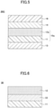
- FIG. 1 is a schematic diagram of a layered structure 10 according to the first embodiment.
- the layered structure 10 includes a polymer substrate 11, and a crystalline functional layer 12 provided on one surface of the substrate 11.
- the functional layer 12 is a layer having a specific function, such as a piezoelectric layer in which micro polarization occurs in response to a pressure applied, a temperature-sensitive magnetic film whose hysteresis characteristics change depending on temperature, or a crystalline nanoporous metal oxide film having a catalytic property.
- the entirety of the layered structure 10 can be made flexible.
- the thinner the functional layer 12 the greater the influence of the surface condition of the underlayer, and cracks penetrating through the functional layer 12 may occur.
- the surface roughness of the substrate 11 on which the functional layer 12 is formed is set in a range suitable for exhibiting the device function.
- the polymer used for the substrate 11 is, for example, polyethylene terephthalate (PET), polyethylene naphthalate (PEN), polycarbonate (PC), an acrylic resin, a cycloolefin polymer, polyimide (PI), or the like.
- PET polyethylene terephthalate
- PEN polyethylene naphthalate
- PC polycarbonate
- acrylic resin acrylic resin
- cycloolefin polymer are colorless and transparent materials.
- the thickness of the substrate 11 is, for example, 20 to 200 ⁇ m, from the viewpoint of satisfying both flexibility and mechanical strength to support the layered structure.
- a piezoelectric layer is formed as the functional layer 12 on the first surface (upper surface in FIG. 1 ) of the substrate 11.
- the piezoelectric layer is formed of, for example, a wurtzite crystal material.
- a wurtzite crystal structure is represented by general formula AB, where A is a positive cation (A n+ ) and B is a negative anion (B n- ). It is desirable to select a wurtzite piezoelectric material which can express piezoelectric properties to a certain degree or higher, and which can be crystallized in a low temperature process at or below 200 °C.
- zinc oxide ZnO
- zinc sulfide ZnS
- zinc selenide ZnSe
- zinc telluride ZnTe
- aluminum nitride AlN
- gallium nitride GaN
- cadmium selenide CdSe
- cadmium telluride CdTe
- silicon carbide SiC
- layers of the selected compounds may be stacked one by one, or alternatively, a single layer may be formed using the targets of the selected compounds.
- the selected one or the combination of two or more of the compounds may be used as the main component, and other components may be optionally added. If a component other than the main component is added, the content of the component added as a sub-component is preferably from 0.1 to 30 at.%.
- a wurtzite material containing ZnO or AlN as the main component is used.
- a metal which that does not cause the main component to exhibit conductivity when incorporated in the main component may be added as a dopant.
- dopants may include silicon (Si), magnesium (Mg), vanadium (V), titanium (Ti), zirconium (Zr), lithium (Li), etc.
- One or a combination of two or more of the above-described dopants may be added. By adding one or more of these metals, the occurrence of cracking can be reduced.
- a transparent wurtzite crystalline material is used for the piezoelectric layer, the layered structure is suitable for use in a display.
- the functional layer 12 In order to ensure the flexibility of the layered structure 10 as a whole, it is desirable for the functional layer 12 to be made thin. However, in the case of the piezoelectric layer, it is difficult to achieve a sufficient level of polarization (namely, piezoelectricity) if the film is too thin.
- the film thickness is, for example, 50 nm to 2 ⁇ m, preferably 200 nm to 1 ⁇ m.
- the surface roughness of the first surface of the substrate 11 is 3 nm or less in terms of arithmetic mean roughness (Ra).
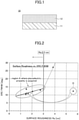
- FIG. 2 is a diagram showing the range of surface roughness of the substrate 11 suitable for achieving a satisfactory piezoelectric property.
- the horizontal axis represents arithmetic mean roughness (Ra), and the vertical axis represents full width at half-maximum (FWHM) of the X-ray Rocking Curve (XRC) expressed in degree.
- the arithmetic mean roughness (Ra) is a parameter of the height or vertical direction, and represents the average value of the unevenness along the reference length.
- a 1 ⁇ m ⁇ 1 ⁇ m surface area is observed by an atomic force microscope (AFM) on various sample substrates.
- AFM atomic force microscope
- the measuring method is not limited to the use of AFM.
- any suitable instrument such as a white interferometer or a stylus meter may be used.
- XRC FWHM is an index representing crystal orientation.
- a ZnO layer having a thickness of 200 nm is formed on each of the sample substrates, and the reflection of the X-rays from the (0002) plane of ZnO is observed by locking curve measurement.
- the XRC FWHM of the reflected light from the (0002) plane indicates the C-axis orientation of the ZnO crystal.
- the smaller the XRC FWHM value the better the crystal orientation and the higher the thickness-direction polarization. It is desirable that the XRC FWHM is less than 15 degrees in order to achieve an acceptable piezoelectric property which allows the device to operate.
- the surface roughness (Ra) of the substrate 11 corresponding to this XRC FWHM range is 3 nm or less.
- a data point D with a surface roughness of 5.6 nm and an XRC FWHM of 12.5 degrees is observed. This data point is due to local protrusions present in the area extracted from the sample substrate. Excluding this data point, the arithmetic mean roughness (Ra) of this area is about 1.8 nm, which is within the region A where satisfactory piezoelectric property is achieved.
- the surface roughness of the substrate 11 is 3 nm or less in order to achieve satisfactory piezoelectric property of the functional layer 12. This applies not only to the piezoelectric film, but also to other functional crystal films such as a temperature-sensitive magnetic layer or a catalyst layer, for achieving good crystal orientation with few pinholes or cracks. If these functional layers 12 are formed on the polymer substrate 11, it is similarly desirable for the surface roughness of the underlying substrate 11 to be 3 nm or less in arithmetic mean roughness.
- Examples of the substrate with the above-described range of surface roughness include PET, PEN, PC, acrylic resin, cycloolefin polymer, polyimide, etc. Substrates made of these materials and having undergone a surface smoothing treatment may also be used.
- FIG. 3 is a schematic diagram of a piezoelectric device 20A to which the layered structure 10 is applied.
- the piezoelectric device 20A has a layered structure 10a in which a piezoelectric layer 12a is provided as the functional layer 12 on the polymer substrate 11.
- a first electrode layer 13 the polymer substrate 11, the piezoelectric layer 12a, and a second electrode layer 14 are stacked in this order.
- the piezoelectric device 20A can be used as a piezo actuator.
- the materials of the first electrode layer 13 and the second electrode layer 14 are not limited as long as they are good conductors.
- a transparent electrode may be used for one or both of the first electrode layer 13 and the second electrode layer 14, depending on the light incident direction and light emitting direction.
- the piezoelectric device 20A is manufactured by, for example, the following process.
- a polymer film having a surface roughness (arithmetic mean roughness Ra) of 3 nm or less is prepared and used as the substrate 11.
- One of the main surfaces of the substrate 11, on which the piezoelectric layer 12a is to be formed, is referred to as "the first surface”.
- the surface roughness (Ra) of the first surface is 3 nm or less.
- the first electrode layer 13 is formed on the surface (back surface in FIG. 3 ) on the opposite side of the substrate 11 from the first surface.
- an indium tin oxide (ITO) film is formed as the first electrode layer 13 by direct current (DC) or radio frequency (RF) magnetron sputtering.
- a ZnO piezoelectric layer 12a having a film thickness of 50 to 200 nm is formed on the first surface of the substrate 11 by, for example, RF magnetron sputtering using a ZnO target.
- the material of the piezoelectric layer 12a is not limited to ZnO, and other materials such as ZnS, ZnSe, ZnTe, AlN, GaN, CdSe, CdTe, SiC, or a combination of two or more of these materials may be used, as described above. Alternatively, one or a combination of two or more of these materials may be used as the main component, and a metal such as Si, Mg, V, Ti, Zr, or Li, which does not cause the piezoelectric layer to exhibit conductivity, may be added.
- the substrate 11 can be used as a part of the functional layer. If a conductive polymer film is used as the substrate 11, the substrate 11 can be used as a part of the electrode.
- the second electrode layer 14 is formed on the piezoelectric layer 12a.
- An ITO film may be formed as the second electrode layer 14 by DC or RF magnetron sputtering, for example.
- the ITO films may be crystallized at a temperature below the melting point or the glass transition point (e.g., 130 °C) of the polymer substrate 11 to reduce the electrical resistance of the first electrode layer 13 and the second electrode layer 14; however, this heat treatment is not essential.
- the piezoelectric layer 12a is formed on the first surface of the substrate 11 having an arithmetic mean roughness Ra of 3 nm, and accordingly, cracks are suppressed and good polarization characteristics are achieved. Further, the piezoelectric device 20A has flexibility as a whole, and the device can be applicable to a wide range of products.
- FIG. 4 is a schematic diagram of a piezoelectric device 20B.
- a polymer film 16 is inserted between the piezoelectric layer 12a and the second electrode layer 14.
- the first electrode layer 13, the polymer substrate 11, the piezoelectric layer 12a, the polymer film 16, and the second electrode layer 14 are stacked in this order.
- the surface roughness of one of the main surfaces (i.e., the first surface) of the substrate 11, on which the piezoelectric layer 12a is formed is 3 nm or less in arithmetic mean roughness (Ra).
- Ra arithmetic mean roughness
- the piezoelectric device 20B is manufactured by, for example, the following process.
- the piezoelectric layer 12a is formed on the first surface of the substrate 11, and the first electrode layer 13 is formed on the surface on the opposite side of the substrate from the first surface, whereby the first part of the device is prepared.
- a second electrode layer 14 is formed on one surface of the polymer film 16 to prepare the second part of the device.
- the other surface of the polymer film 16 of the second part is brought so as to face the surface of the piezoelectric layer 12a of the first part, and bonded to the first part with an adhesive (not shown).
- FIG. 5 is a schematic diagram of a piezoelectric device 20C.
- the polymer film 16 is provided on the second electrode layer 14. That is, the first electrode layer 13, the polymer substrate 11, the piezoelectric layer 12a, the second electrode layer 14, and the polymer film 16 are stacked in this order.
- the surface roughness of at least one of the main surfaces of the substrate 11, namely, the surface roughness of the first surface on which the piezoelectric layer 12a is formed is 3 nm or less in arithmetic average roughness Ra.
- the piezoelectric device 20C is manufactured by, for example, the following process.
- the piezoelectric layer 12a is formed on the first surface of the substrate 11, and the first electrode layer 13 is formed on the surface on the opposite sde of the substrate 11 from the first surface to prepare the first part of the device. Meanwhile, a second electrode layer 14 is formed on one surface of the polymer film 16 to prepare the second part of the device.
- the second electrode layer 14 of the second part is brought so as to face the surface of the piezoelectric layer 12a of the first part, and bonded to the first part with an adhesive (not shown).
- the flexibility can be enhanced and the occurrence of cracks in the piezoelectric layer 12a can be suppressed.
- the uppermost polymer film 16 can function as a protective film.
- FIG. 6 is a schematic diagram of a layered structure 30 according to the second embodiment.
- the layered structure 30 includes a polymer substrate 11, an amorphous layer 33 provided on the substrate 11, and a crystalline functional layer 12 provided on the amorphous layer 33.
- the surface roughness of the substrate 11 is 3 nm or less in arithmetic average roughness Ra.
- the crystal orientation of the functional layer 12 is further improved by inserting an amorphous layer 33 between the polymer substrate 11 and the functional layer 12.
- the "amorphous layer” does not have to be 100% amorphous, and it refers to a layer in which 90% or more, preferably 95% or more is amorphous, and in which the interface with the functional layer 12 is amorphous.
- the amorphous layer 33 may be formed of a transparent metal oxide.
- the thickness of the amorphous layer 33 is, for example, 3 to 200 nm, preferably 5 to 100 nm.
- the amorphous layer 33 is an insulating layer, for example, silicon oxide (SiOx), silicon nitride (SiN), aluminum nitride (AlN), aluminum oxide (A1203), gallium nitride (GaN), gallium oxide (Ga 2 O 3 ), etc. can be used.
- SiOx silicon oxide
- SiN silicon nitride
- AlN aluminum nitride
- AlN aluminum oxide
- AlN aluminum oxide
- GaN gallium nitride
- Ga 2 O 3 gallium oxide
- Ga 2 O 3 gallium oxide
- the amorphous layer 33 is formed of an insulating organic film, an acrylic resin, a urethane resin, a melamine resin, an alkyd resin, a siloxane-based polymer, or the like can be used.
- an acrylic resin, a urethane resin, a melamine resin, an alkyd resin, a siloxane-based polymer, or the like can be used.
- a thermosetting resin composed of a mixture of a melamine resin, an alkyd resin and an organic silane condensate may be used.
- the amorphous layer 33 may be formed of an organic film to which a conductive dopant is added, and it may be used as an electrode. Alternatively, the amorphous layer 33 may be formed of a conductive metal oxide and used as an electrode.
- the conductive oxide ITO, indium zinc oxide (IZO), or the like can be used. These materials are also suitable for devices that require light transmissive characteristics.
- the amorphous layer 33 of the conductive oxide can be formed by, for example, DC or RF magnetron sputtering to a thickness of 5 to 200 nm, more preferably 10 to 100 nm.
- the content of tin (Sn), namely the content ratio Sn/(In + Sn) may be 5 to 15 wt%.
- ITO is transparent to visible light, and an amorphous film can be formed by sputtering at room temperature.
- the content of zinc (Zn), namely the content ratio Zn/(In + Zn) may be around 10 wt%. At this content ratio, IZO is also transparent to visible light, and an amorphous film can be formed by sputtering at room temperature.
- the amorphous layer 33 formed of the above-described materials has satisfactory surface smoothness, and allows the c-axis of the wurtzite-type material formed on the amorphous layer to be oriented in the growth direction.
- the amorphous layer has a high gas barrier property and can reduce the influence of gas derived from the polymer substrate 11 during film formation.
- FIG. 7 is a schematic diagram of the piezoelectric device 40 using the layered structure 30a in which the functional layer 12 is formed as the piezoelectric layer 12a.
- the amorphous layer 33, the piezoelectric layer 12a, and the electrode layer 14 are stacked in this order on the polymer substrate 11.
- the amorphous layer 33 is formed of a conductive oxide and functions as a first electrode layer.
- the piezoelectric device 40 is manufactured by, for example, the following process.
- a polymer film having a surface roughness (arithmetic mean roughness Ra) of 3 nm or less of the first surface is prepared, which is used as the substrate 11.
- An amorphous layer 33 having a thickness of 5 to 100 nm is formed of a conductive oxide such as ITO, IZO, IZTO, or IGZO on the first surface of the substrate 11 by DC or RF magnetron sputtering.
- a piezoelectric layer 12a having a film thickness of 50 to 200 nm is formed on the amorphous layer 33 by, for example, RF magnetron sputtering.
- a second electrode layer 14 is formed on the piezoelectric layer 12a.
- the amorphous layer 33 is provided on the smooth polymer substrate 11 having an arithmetic mean roughness Ra of 3 nm or less, and the piezoelectric layer 12a is provided on the amorphous layer 33.
- the crystal orientation of the piezoelectric layer 12a is further improved, and good piezoelectric characteristics can be obtained.
- FIG. 8 is a schematic diagram of a layered structure 30b of the third embodiment and the piezoelectric device 50 using the same.
- the layered structure 30b includes a polymer substrate 11, an amorphous layer 33b provided on the substrate 11, a first electrode layer 13 provided on the amorphous layer 33b, and a piezoelectric layer 12a provided on the first electrode layer 13.
- the piezoelectric layer 12a is an example of the crystalline functional layer 12, and has a film thickness of 50 to 200 nm.
- the surface roughness of the polymer substrate 11 is 3 nm or less in arithmetic average roughness Ra.
- the amorphous layer 33b is provided between the substrate 11 and the first electrode layer 13, which is provided under the piezoelectric layer 12a.
- the amorphous layer 33b is formed of an inorganic material, an organic material, or a mixture of an inorganic material and an organic material.
- the "amorphous layer” does not have to be 100% amorphous, and it refers to a layer in which 90% or more, preferably 95% or more is amorphous, and in which the interface with the functional layer 12 is amorphous.
- the crystal orientation of the first electrode layer 13 is improved, and the crystal orientation of the piezoelectric layer 12a formed on the first electrode layer 13 is further improved.
- the piezoelectric device 50 can be fabricated by forming the second electrode layer 14 on the top of the layered structure 30b. Because the piezoelectric device 50 uses the layered structure 30b, the crystal orientation of the piezoelectric layer 12a is improved, and the piezoelectric characteristics are improved.
- the present invention is not limited to the above-described exemplified structures.
- the layered structure 30 of FIG. 6 may be applied to the device configuration of FIG. 4 or FIG. 5 .
- the amorphous layer 33 of a conductive organic material By forming the amorphous layer 33 of a conductive organic material, the flexibility of the entire piezoelectric device can be further improved.
Landscapes
- Engineering & Computer Science (AREA)
- Manufacturing & Machinery (AREA)
- Chemical & Material Sciences (AREA)
- Ceramic Engineering (AREA)
- Laminated Bodies (AREA)
- Physical Vapour Deposition (AREA)
- Piezo-Electric Transducers For Audible Bands (AREA)
Abstract
Description
- The present invention relates to a layered structure, a piezoelectric device using the same, and a method of manufacturing a piezoelectric device.
- Conventionally, a piezoelectric device, which makes use of the piezoelectric effect of a substance has been adopted. The piezoelectric effect is a phenomenon in which microscopic polarization occurs in proportion to a pressure applied to a substance. Various sensors such as pressure sensors, acceleration sensors, or acoustic emission (AE) sensors for detecting elastic waves have been manufactured by utilizing the piezoelectric effect.
- In recent years, touch panels have been used as input interfaces of information processing devices such as smartphones, and applying piezoelectric devices to touch panels is increasing. A touch panel is integrated into the display device of an information processing device, and high transparency to visible light is required to improve the visibility. On the other hand, it is desirable for the piezoelectric layer to be highly responsive to pressure in order to accurately detect operations by a finger.
- A structure in which a piezoelectric layer formed of a metal nitride having a Wurtzite crystal structure is provided on a flexible insulating film is known (see, for example, Patent Document 1). A structure in which an orientation control layer is inserted between a plastic layer and a piezoelectric layer is also known (see, for example, Patent Document 2).
-
- Patent Document 1:
JP Patent Application Laid-open Publication No. 2018-137268 - Patent Document 2:
JP Patent Application Laid-open Publication No. 2018-170503 - When a crystalline functional layer is formed on the surface of a polymer substrate, microcracking often occurs in the functional layer due to the surface roughness of, or foreign substances on the polymer substrate. Even if an electrode film is inserted between the polymer substrate and the crystalline functional layer, it is difficult for the electrode film to absorb the roughness of the substrate surface, and unevenness remains on the surface of the electrode, reflecting the surface roughness of the substrate.
- If cracks, pinholes, or the like occur in the functional layer due to the surface roughness of the underlayer, a leakage path which causes electrical short-circuit between the top and bottom electrodes is likely to be produced. This phenomenon becomes more prominent as the functional layer becomes thinner. Examples of the functional layer include a piezoelectric layer, a moisture-sensitive film, an odor-sensitive film, etc. If the functional layer cracks, the performance of the device deteriorates. Upon occurrence of a leakage path, the device may not function any longer.
- An objective of the invention is to provide a layered structure capable of suppressing cracks from occurring in a functional layer, while maintaining the flexibility, and to provide a piezoelectric device using such a layered structure and a method of manufacturing the piezoelectric device.
- In the first aspect of the invention, a layered structure includes a polymer substrate, and a crystalline functional layer formed on the first surface of the substrate. The surface roughness of the first surface of the substrate is 3 nm or less in terms of arithmetic mean roughness (Ra).
- In a second aspect of the invention, a piezoelectric device includes a polymer substrate, a piezoelectric layer formed on the first surface of the substrate, and a pair of electrodes provided on an upper side and a lower side of the piezoelectric layer in the layered direction. The surface roughness of the first surface of the substrate is 3 nm or less in terms of arithmetic mean roughness (Ra).
- According to the above-described configurations, occurrence of cracks can be suppressed in the functional layer, while maintaining the flexibility of the layered structure.
-
-
FIG. 1 is a schematic diagram of a layered structure according to a first embodiment; -
FIG. 2 is a diagram showing surface roughness required for a device characteristic; -
FIG. 3 shows an example configuration of a piezoelectric device; -
FIG. 4 shows another example configuration of the piezoelectric device; -
FIG. 5 shows still another example configuration of the piezoelectric device; -
FIG. 6 is a schematic diagram of a layered structure according to a second embodiment; -
FIG. 7 shows an example configuration of a piezoelectric device using the layered structure ofFIG. 6 ; and -
FIG. 8 shows an example configuration of a piezoelectric device using a layered structure according to a third embodiment. -
FIG. 1 is a schematic diagram of alayered structure 10 according to the first embodiment. Thelayered structure 10 includes apolymer substrate 11, and a crystallinefunctional layer 12 provided on one surface of thesubstrate 11. Thefunctional layer 12 is a layer having a specific function, such as a piezoelectric layer in which micro polarization occurs in response to a pressure applied, a temperature-sensitive magnetic film whose hysteresis characteristics change depending on temperature, or a crystalline nanoporous metal oxide film having a catalytic property. - By using the
polymer substrate 11, the entirety of thelayered structure 10 can be made flexible. In order to increase the flexibility, it may be desirable to reduce the thickness of thefunctional layer 12 to such an extent not to damage the expression of the function. However, the thinner thefunctional layer 12, the greater the influence of the surface condition of the underlayer, and cracks penetrating through thefunctional layer 12 may occur. - In the embodiment, the surface roughness of the
substrate 11 on which thefunctional layer 12 is formed is set in a range suitable for exhibiting the device function. - The polymer used for the
substrate 11 is, for example, polyethylene terephthalate (PET), polyethylene naphthalate (PEN), polycarbonate (PC), an acrylic resin, a cycloolefin polymer, polyimide (PI), or the like. Among these, polyethylene terephthalate (PET), polyethylene naphthalate (PEN), polycarbonate (PC), acrylic resin, and cycloolefin polymer are colorless and transparent materials. - The thickness of the
substrate 11 is, for example, 20 to 200 µm, from the viewpoint of satisfying both flexibility and mechanical strength to support the layered structure. - A piezoelectric layer is formed as the
functional layer 12 on the first surface (upper surface inFIG. 1 ) of thesubstrate 11. The piezoelectric layer is formed of, for example, a wurtzite crystal material. - A wurtzite crystal structure is represented by general formula AB, where A is a positive cation (An+) and B is a negative anion (Bn-). It is desirable to select a wurtzite piezoelectric material which can express piezoelectric properties to a certain degree or higher, and which can be crystallized in a low temperature process at or below 200 °C. For example, zinc oxide (ZnO), zinc sulfide (ZnS), zinc selenide (ZnSe), zinc telluride (ZnTe), aluminum nitride (AlN), gallium nitride (GaN), cadmium selenide (CdSe), cadmium telluride (CdTe), silicon carbide (SiC), etc. can be suitably used. One or a combination of two or more of the above-described compounds may be used
- When two or more of the compounds are combined, layers of the selected compounds may be stacked one by one, or alternatively, a single layer may be formed using the targets of the selected compounds. The selected one or the combination of two or more of the compounds may be used as the main component, and other components may be optionally added. If a component other than the main component is added, the content of the component added as a sub-component is preferably from 0.1 to 30 at.%.
- For example, a wurtzite material containing ZnO or AlN as the main component is used. A metal which that does not cause the main component to exhibit conductivity when incorporated in the main component may be added as a dopant. Such dopants may include silicon (Si), magnesium (Mg), vanadium (V), titanium (Ti), zirconium (Zr), lithium (Li), etc. One or a combination of two or more of the above-described dopants may be added. By adding one or more of these metals, the occurrence of cracking can be reduced. When a transparent wurtzite crystalline material is used for the piezoelectric layer, the layered structure is suitable for use in a display.
- In order to ensure the flexibility of the
layered structure 10 as a whole, it is desirable for thefunctional layer 12 to be made thin. However, in the case of the piezoelectric layer, it is difficult to achieve a sufficient level of polarization (namely, piezoelectricity) if the film is too thin. For afunctional layer 12 made of a wurtzite piezoelectric material, the film thickness is, for example, 50 nm to 2 µm, preferably 200 nm to 1 µm. - The surface roughness of the first surface of the
substrate 11 is 3 nm or less in terms of arithmetic mean roughness (Ra). By using apolymer substrate 11 with a smooth surface, the occurrence of cracking in the functional layer can be suppressed because of the reduced influence from the underlying structure. -
FIG. 2 is a diagram showing the range of surface roughness of thesubstrate 11 suitable for achieving a satisfactory piezoelectric property. The horizontal axis represents arithmetic mean roughness (Ra), and the vertical axis represents full width at half-maximum (FWHM) of the X-ray Rocking Curve (XRC) expressed in degree. - The arithmetic mean roughness (Ra) is a parameter of the height or vertical direction, and represents the average value of the unevenness along the reference length. A part of the roughness curve, which is acquired by measuring the state of the interface using a roughness meter, is extracted along the reference length. In particular, a 1 µm × 1 µm surface area is observed by an atomic force microscope (AFM) on various sample substrates. Although an AFM is used to measure the arithmetic mean roughness (Ra) in this example, the measuring method is not limited to the use of AFM. As long as the arithmetic mean roughness (Ra) can be evaluated, any suitable instrument such as a white interferometer or a stylus meter may be used.
- XRC FWHM is an index representing crystal orientation. In this example, a ZnO layer having a thickness of 200 nm is formed on each of the sample substrates, and the reflection of the X-rays from the (0002) plane of ZnO is observed by locking curve measurement. The XRC FWHM of the reflected light from the (0002) plane indicates the C-axis orientation of the ZnO crystal. The smaller the XRC FWHM value, the better the crystal orientation and the higher the thickness-direction polarization. It is desirable that the XRC FWHM is less than 15 degrees in order to achieve an acceptable piezoelectric property which allows the device to operate. The surface roughness (Ra) of the
substrate 11 corresponding to this XRC FWHM range is 3 nm or less. - In
FIG. 2 , a data point D with a surface roughness of 5.6 nm and an XRC FWHM of 12.5 degrees is observed. This data point is due to local protrusions present in the area extracted from the sample substrate. Excluding this data point, the arithmetic mean roughness (Ra) of this area is about 1.8 nm, which is within the region A where satisfactory piezoelectric property is achieved. - From this measurement result, it is derived that the surface roughness of the
substrate 11 is 3 nm or less in order to achieve satisfactory piezoelectric property of thefunctional layer 12. This applies not only to the piezoelectric film, but also to other functional crystal films such as a temperature-sensitive magnetic layer or a catalyst layer, for achieving good crystal orientation with few pinholes or cracks. If thesefunctional layers 12 are formed on thepolymer substrate 11, it is similarly desirable for the surface roughness of theunderlying substrate 11 to be 3 nm or less in arithmetic mean roughness. - Examples of the substrate with the above-described range of surface roughness include PET, PEN, PC, acrylic resin, cycloolefin polymer, polyimide, etc. Substrates made of these materials and having undergone a surface smoothing treatment may also be used.
-
FIG. 3 is a schematic diagram of apiezoelectric device 20A to which the layeredstructure 10 is applied. Thepiezoelectric device 20A has a layeredstructure 10a in which apiezoelectric layer 12a is provided as thefunctional layer 12 on thepolymer substrate 11. In thepiezoelectric device 20A, afirst electrode layer 13, thepolymer substrate 11, thepiezoelectric layer 12a, and asecond electrode layer 14 are stacked in this order. - When pressure or tensile stress is applied to the
piezoelectric device 20A, polarization proportional to the pressure occurs in thepiezoelectric layer 12a. By extracting the electric charges as an electric current through thefirst electrode layer 13 and thesecond electrode layer 14, the applied pressure or tensile stress can be detected. - Further, by applying a voltage to the
piezoelectric layer 12a via thefirst electrode layer 13 and thesecond electrode layer 14, an inverse piezoelectric effect that causes thepiezoelectric layer 12a to deform in the layered direction may be utilized. In this case, thepiezoelectric device 20A can be used as a piezo actuator. - The materials of the
first electrode layer 13 and thesecond electrode layer 14 are not limited as long as they are good conductors. When thepiezoelectric device 20A is applied to a light transmissive (optically transparent) device, a transparent electrode may be used for one or both of thefirst electrode layer 13 and thesecond electrode layer 14, depending on the light incident direction and light emitting direction. - The
piezoelectric device 20A is manufactured by, for example, the following process. A polymer film having a surface roughness (arithmetic mean roughness Ra) of 3 nm or less is prepared and used as thesubstrate 11. One of the main surfaces of thesubstrate 11, on which thepiezoelectric layer 12a is to be formed, is referred to as "the first surface". The surface roughness (Ra) of the first surface is 3 nm or less. - The
first electrode layer 13 is formed on the surface (back surface inFIG. 3 ) on the opposite side of thesubstrate 11 from the first surface. For example, an indium tin oxide (ITO) film is formed as thefirst electrode layer 13 by direct current (DC) or radio frequency (RF) magnetron sputtering. - A
ZnO piezoelectric layer 12a having a film thickness of 50 to 200 nm is formed on the first surface of thesubstrate 11 by, for example, RF magnetron sputtering using a ZnO target. The material of thepiezoelectric layer 12a is not limited to ZnO, and other materials such as ZnS, ZnSe, ZnTe, AlN, GaN, CdSe, CdTe, SiC, or a combination of two or more of these materials may be used, as described above. Alternatively, one or a combination of two or more of these materials may be used as the main component, and a metal such as Si, Mg, V, Ti, Zr, or Li, which does not cause the piezoelectric layer to exhibit conductivity, may be added. - If a high-dielectric polymer film is used as the
substrate 11, thesubstrate 11 can be used as a part of the functional layer. If a conductive polymer film is used as thesubstrate 11, thesubstrate 11 can be used as a part of the electrode. - The
second electrode layer 14 is formed on thepiezoelectric layer 12a. An ITO film may be formed as thesecond electrode layer 14 by DC or RF magnetron sputtering, for example. - After the
second electrode layer 14 is formed, the ITO films may be crystallized at a temperature below the melting point or the glass transition point (e.g., 130 °C) of thepolymer substrate 11 to reduce the electrical resistance of thefirst electrode layer 13 and thesecond electrode layer 14; however, this heat treatment is not essential. - In the
piezoelectric device 20A, thepiezoelectric layer 12a is formed on the first surface of thesubstrate 11 having an arithmetic mean roughness Ra of 3 nm, and accordingly, cracks are suppressed and good polarization characteristics are achieved. Further, thepiezoelectric device 20A has flexibility as a whole, and the device can be applicable to a wide range of products. -
FIG. 4 is a schematic diagram of apiezoelectric device 20B. In thepiezoelectric device 20B, apolymer film 16 is inserted between thepiezoelectric layer 12a and thesecond electrode layer 14. In other words, in thepiezoelectric device 20B, thefirst electrode layer 13, thepolymer substrate 11, thepiezoelectric layer 12a, thepolymer film 16, and thesecond electrode layer 14 are stacked in this order. - As in
FIG. 3 , the surface roughness of one of the main surfaces (i.e., the first surface) of thesubstrate 11, on which thepiezoelectric layer 12a is formed, is 3 nm or less in arithmetic mean roughness (Ra). When thepiezoelectric layer 12a is formed on the first surface of thepolymer substrate 11, cracks can be suppressed, and the polarization characteristics (or piezoelectricity) can be maintained satisfactorily. - The
piezoelectric device 20B is manufactured by, for example, the following process. Thepiezoelectric layer 12a is formed on the first surface of thesubstrate 11, and thefirst electrode layer 13 is formed on the surface on the opposite side of the substrate from the first surface, whereby the first part of the device is prepared. Meanwhile, asecond electrode layer 14 is formed on one surface of thepolymer film 16 to prepare the second part of the device. - The other surface of the
polymer film 16 of the second part is brought so as to face the surface of thepiezoelectric layer 12a of the first part, and bonded to the first part with an adhesive (not shown). - With this configuration, flexibility can be enhanced by providing polymer layers on both sides of the
piezoelectric layer 12a in the layered direction. Further, even if a fine crack occurs in thepiezoelectric layer 12a, occurrence of a leakage path which causes electrical short-circuits between the top and bottom electrodes can be prevented. -
FIG. 5 is a schematic diagram of a piezoelectric device 20C. In the piezoelectric device 20C, thepolymer film 16 is provided on thesecond electrode layer 14. That is, thefirst electrode layer 13, thepolymer substrate 11, thepiezoelectric layer 12a, thesecond electrode layer 14, and thepolymer film 16 are stacked in this order. - Similar to
FIG. 3 and FIG. 4 , the surface roughness of at least one of the main surfaces of thesubstrate 11, namely, the surface roughness of the first surface on which thepiezoelectric layer 12a is formed, is 3 nm or less in arithmetic average roughness Ra. By forming thepiezoelectric layer 12a on the first surface of thepolymer substrate 11, cracks can be suppressed, and the polarization characteristics (or piezoelectricity) can be maintained satisfactorily. - The piezoelectric device 20C is manufactured by, for example, the following process. The
piezoelectric layer 12a is formed on the first surface of thesubstrate 11, and thefirst electrode layer 13 is formed on the surface on the opposite sde of thesubstrate 11 from the first surface to prepare the first part of the device. Meanwhile, asecond electrode layer 14 is formed on one surface of thepolymer film 16 to prepare the second part of the device. - The
second electrode layer 14 of the second part is brought so as to face the surface of thepiezoelectric layer 12a of the first part, and bonded to the first part with an adhesive (not shown). - In this configuration, by arranging the polymer material layers above and below the
piezoelectric layer 12a in the layered direction, the flexibility can be enhanced and the occurrence of cracks in thepiezoelectric layer 12a can be suppressed. Theuppermost polymer film 16 can function as a protective film. -
FIG. 6 is a schematic diagram of alayered structure 30 according to the second embodiment. The layeredstructure 30 includes apolymer substrate 11, anamorphous layer 33 provided on thesubstrate 11, and a crystallinefunctional layer 12 provided on theamorphous layer 33. - The surface roughness of the
substrate 11 is 3 nm or less in arithmetic average roughness Ra. By using apolymer base material 11 having such a smooth surface, the entirety of the layeredstructure 30 can be made flexible and the crystal orientation of thefunctional layer 12 can be improved. - In the second embodiment, the crystal orientation of the
functional layer 12 is further improved by inserting anamorphous layer 33 between thepolymer substrate 11 and thefunctional layer 12. The "amorphous layer" does not have to be 100% amorphous, and it refers to a layer in which 90% or more, preferably 95% or more is amorphous, and in which the interface with thefunctional layer 12 is amorphous. - If the
layered structure 30 is applied to a device requiring transparency, theamorphous layer 33 may be formed of a transparent metal oxide. The thickness of theamorphous layer 33 is, for example, 3 to 200 nm, preferably 5 to 100 nm. By forming the crystallinefunctional layer 12 on theamorphous layer 33, thefunctional layer 12 can be grown without being affected by the underlying crystal structure. Thefunctional layer 12 with less strain and good crystal orientation has few defects, and occurrence of cracks is suppressed. - If the
amorphous layer 33 is an insulating layer, for example, silicon oxide (SiOx), silicon nitride (SiN), aluminum nitride (AlN), aluminum oxide (A1203), gallium nitride (GaN), gallium oxide (Ga2O3), etc. can be used. Alternatively, ZnO to which Al2O3 and SiOx are added, or GaN, AlN, ZnO or the like to which at least one of Al2O3, Ga2O3, SiOx and SiN is added may be used. - If the
amorphous layer 33 is formed of an insulating organic film, an acrylic resin, a urethane resin, a melamine resin, an alkyd resin, a siloxane-based polymer, or the like can be used. As the organic substance, a thermosetting resin composed of a mixture of a melamine resin, an alkyd resin and an organic silane condensate may be used. - The
amorphous layer 33 may be formed of an organic film to which a conductive dopant is added, and it may be used as an electrode. Alternatively, theamorphous layer 33 may be formed of a conductive metal oxide and used as an electrode. - As the conductive oxide, ITO, indium zinc oxide (IZO), or the like can be used. These materials are also suitable for devices that require light transmissive characteristics. The
amorphous layer 33 of the conductive oxide can be formed by, for example, DC or RF magnetron sputtering to a thickness of 5 to 200 nm, more preferably 10 to 100 nm. - When ITO is used, the content of tin (Sn), namely the content ratio Sn/(In + Sn) may be 5 to 15 wt%. At a content ratio within this range, ITO is transparent to visible light, and an amorphous film can be formed by sputtering at room temperature.
- When IZO is used, the content of zinc (Zn), namely the content ratio Zn/(In + Zn) may be around 10 wt%. At this content ratio, IZO is also transparent to visible light, and an amorphous film can be formed by sputtering at room temperature.
- The
amorphous layer 33 formed of the above-described materials has satisfactory surface smoothness, and allows the c-axis of the wurtzite-type material formed on the amorphous layer to be oriented in the growth direction. In addition, the amorphous layer has a high gas barrier property and can reduce the influence of gas derived from thepolymer substrate 11 during film formation. -
FIG. 7 is a schematic diagram of thepiezoelectric device 40 using the layeredstructure 30a in which thefunctional layer 12 is formed as thepiezoelectric layer 12a. In thepiezoelectric device 40, theamorphous layer 33, thepiezoelectric layer 12a, and theelectrode layer 14 are stacked in this order on thepolymer substrate 11. Theamorphous layer 33 is formed of a conductive oxide and functions as a first electrode layer. - The
piezoelectric device 40 is manufactured by, for example, the following process. A polymer film having a surface roughness (arithmetic mean roughness Ra) of 3 nm or less of the first surface is prepared, which is used as thesubstrate 11. Anamorphous layer 33 having a thickness of 5 to 100 nm is formed of a conductive oxide such as ITO, IZO, IZTO, or IGZO on the first surface of thesubstrate 11 by DC or RF magnetron sputtering. - A
piezoelectric layer 12a having a film thickness of 50 to 200 nm is formed on theamorphous layer 33 by, for example, RF magnetron sputtering. - A
second electrode layer 14 is formed on thepiezoelectric layer 12a. - In this configuration, the
amorphous layer 33 is provided on thesmooth polymer substrate 11 having an arithmetic mean roughness Ra of 3 nm or less, and thepiezoelectric layer 12a is provided on theamorphous layer 33. The crystal orientation of thepiezoelectric layer 12a is further improved, and good piezoelectric characteristics can be obtained. -
FIG. 8 is a schematic diagram of alayered structure 30b of the third embodiment and thepiezoelectric device 50 using the same. Thelayered structure 30b includes apolymer substrate 11, anamorphous layer 33b provided on thesubstrate 11, afirst electrode layer 13 provided on theamorphous layer 33b, and apiezoelectric layer 12a provided on thefirst electrode layer 13. Thepiezoelectric layer 12a is an example of the crystallinefunctional layer 12, and has a film thickness of 50 to 200 nm. - The surface roughness of the
polymer substrate 11 is 3 nm or less in arithmetic average roughness Ra. By using apolymer substrate 11 with such a smooth surface, the entirety of thelayered structure 30b can be flexible, and the crystal orientation of thepiezoelectric layer 12a is improved. - In the third embodiment, the
amorphous layer 33b is provided between thesubstrate 11 and thefirst electrode layer 13, which is provided under thepiezoelectric layer 12a. Theamorphous layer 33b is formed of an inorganic material, an organic material, or a mixture of an inorganic material and an organic material. The "amorphous layer" does not have to be 100% amorphous, and it refers to a layer in which 90% or more, preferably 95% or more is amorphous, and in which the interface with thefunctional layer 12 is amorphous. - By providing the
amorphous layer 33 under thefirst electrode layer 13, the crystal orientation of thefirst electrode layer 13 is improved, and the crystal orientation of thepiezoelectric layer 12a formed on thefirst electrode layer 13 is further improved. - The
piezoelectric device 50 can be fabricated by forming thesecond electrode layer 14 on the top of thelayered structure 30b. Because thepiezoelectric device 50 uses thelayered structure 30b, the crystal orientation of thepiezoelectric layer 12a is improved, and the piezoelectric characteristics are improved. - Although specific embodiments of the present invention have been described, the present invention is not limited to the above-described exemplified structures. For example, the layered
structure 30 ofFIG. 6 may be applied to the device configuration ofFIG. 4 orFIG. 5 . By forming theamorphous layer 33 of a conductive organic material, the flexibility of the entire piezoelectric device can be further improved. - The present application is based upon and claims priority to the earlier
Japanese Patent Application No. 2019-052877 filed March 20, 2019 -
- 10, 10a, 30, 30a, 30b: layered structure
- 11: substrate
- 12: functional layer
- 12a: piezoelectric layer
- 13: first electrode layer
- 14: second electrode layer
- 16: polymer film
- 20A-20C, 40, 50: piezoelectric device
- 33: amorphous layer
Claims (14)
- A layered structure comprising:a polymer substrate;a crystalline functional layer formed on a first surface of the substrate,wherein a surface roughness of the first surface of the substrate is 3 nm or less in arithmetic mean roughness (Ra).
- The layered structure as claimed in claim 1, further comprising:an amorphous layer provided between the substrate and the functional layer.
- The layered structure as claimed in claim 2, wherein the amorphous layer is an inorganic conductive layer or organic conductive layer.
- A piezoelectric device comprising:a polymer substrate;a piezoelectric layer formed on a first surface of the substrate; anda pair of electrodes including an upper electrode and a lower electrode, the upper electrode being provided on an upper side of the piezoelectric layer, and the lower electrode being provided on a lower side of the piezoelectric layer in a layered direction,wherein a surface roughness of the first surface of the substrate is 3 nm or less in arithmetic mean roughness (Ra).
- The piezoelectric device as claimed in claim 4, wherein, the lower electrode is an amorphous conductive layer.
- The piezoelectric device as claimed in claim 5, wherein the amorphous conductive layer is formed of an oxide conductor or a conductive organic material.
- The piezoelectric device as claimed in claim 5 or 6, wherein the lower electrode is provided between the substrate and the piezoelectric layer.
- The piezoelectric device as claimed in claim 4, wherein the amorphous conductive layer is provided between the substrate and the lower electrode.
- The piezoelectric device as claimed in claim 8, wherein the amorphous conductive layer is formed of an inorganic material, an organic material, or a mixture of an inorganic material and an organic material.
- The piezoelectric device as claimed in any one of claims 4 to 9, wherein a thickness of the substrate is 20 to 200 µm.
- The piezoelectric device as claimed in any one of claims 4 to 10, wherein a thickness of the piezoelectric layer is 50 nm to 2 µm.
- A method of manufacturing a piezoelectric device, comprising:forming a piezoelectric layer on a first surface of a polymer substrate, a surface roughness of the first surface being 3 nm or less in arithmetic mean roughness (Ra);providing a pair of electrodes on either side of the piezoelectric layer.
- The method as claimed in claim 12, further comprising:forming an amorphous layer on the first surface of the polymer substrate;forming the piezoelectric layer on the amorphous layer;forming an upper electrode on the piezoelectric layer,wherein the amorphous layer functions as a lower electrode.
- The method as claimed in claim 12,forming an amorphous layer on the first surface of the polymer substrate;forming a lower electrode on the amorphous layer;forming the piezoelectric layer on the lower electrode; andforming an upper electrode on the piezoelectric layer.
Applications Claiming Priority (2)
| Application Number | Priority Date | Filing Date | Title |
|---|---|---|---|
| JP2019052877A JP7325981B2 (en) | 2019-03-20 | 2019-03-20 | Laminate, piezoelectric device using same, and method for manufacturing piezoelectric device |
| PCT/JP2020/010177 WO2020189397A1 (en) | 2019-03-20 | 2020-03-10 | Laminate, piezoelectric device in which same is used, and method for manufacturing piezoelectric device |
Publications (3)
| Publication Number | Publication Date |
|---|---|
| EP3943292A1 true EP3943292A1 (en) | 2022-01-26 |
| EP3943292A4 EP3943292A4 (en) | 2023-01-04 |
| EP3943292B1 EP3943292B1 (en) | 2024-07-10 |
Family
ID=72519797
Family Applications (1)
| Application Number | Title | Priority Date | Filing Date |
|---|---|---|---|
| EP20772561.5A Active EP3943292B1 (en) | 2019-03-20 | 2020-03-10 | Laminated piezoelectric device, and a method for manufacturing the piezoelectric device |
Country Status (6)
| Country | Link |
|---|---|
| US (1) | US12414472B2 (en) |
| EP (1) | EP3943292B1 (en) |
| JP (1) | JP7325981B2 (en) |
| KR (1) | KR102715824B1 (en) |
| CN (1) | CN113573897B (en) |
| WO (1) | WO2020189397A1 (en) |
Families Citing this family (1)
| Publication number | Priority date | Publication date | Assignee | Title |
|---|---|---|---|---|
| US20240180042A1 (en) * | 2022-11-28 | 2024-05-30 | University of New Mexico Rainforest Innovations | Earth-abundant dopants for piezoelectric enhancement in wurtzite crystals |
Family Cites Families (14)
| Publication number | Priority date | Publication date | Assignee | Title |
|---|---|---|---|---|
| JP4240445B2 (en) | 2002-05-31 | 2009-03-18 | 独立行政法人産業技術総合研究所 | Piezoelectric element using ultra-oriented aluminum nitride thin film and manufacturing method thereof |
| US7323805B2 (en) * | 2004-01-28 | 2008-01-29 | Kabushiki Kaisha Toshiba | Piezoelectric thin film device and method for manufacturing the same |
| JP5198131B2 (en) | 2007-05-14 | 2013-05-15 | 富士フイルム株式会社 | Barrier film and element |
| US20130320813A1 (en) * | 2012-06-04 | 2013-12-05 | Tdk Corporation | Dielectric device |
| JP6091281B2 (en) | 2013-03-25 | 2017-03-08 | 住友化学株式会社 | Piezoelectric thin film multilayer substrate |
| WO2015166963A1 (en) * | 2014-04-30 | 2015-11-05 | 日東電工株式会社 | Transparent conductive film and method for producing same |
| CN106460153B (en) * | 2014-04-30 | 2019-05-10 | 日东电工株式会社 | Transparent conductive film and method for producing the same |
| WO2017209080A1 (en) * | 2016-05-30 | 2017-12-07 | 日東電工株式会社 | Piezoelectric film |
| JP7031181B2 (en) * | 2016-09-13 | 2022-03-08 | 東ソー株式会社 | Gallium nitride based film and its manufacturing method |
| JP2018093132A (en) * | 2016-12-07 | 2018-06-14 | 日本電気硝子株式会社 | Piezoelectric device |
| JP6747334B2 (en) | 2017-02-20 | 2020-08-26 | 三菱マテリアル株式会社 | Electronic device and manufacturing method thereof |
| WO2018163884A1 (en) * | 2017-03-10 | 2018-09-13 | コニカミノルタ株式会社 | Transparent electrode substrate film and method for producing same |
| JP7053313B2 (en) * | 2017-03-29 | 2022-04-12 | 日東電工株式会社 | Piezoelectric device and manufacturing method of piezoelectric device |
| JP6992340B2 (en) | 2017-09-13 | 2022-01-13 | 凸版印刷株式会社 | Web slack measurement mechanism and web transfer device equipped with it |
-
2019
- 2019-03-20 JP JP2019052877A patent/JP7325981B2/en active Active
-
2020
- 2020-03-10 KR KR1020217029141A patent/KR102715824B1/en active Active
- 2020-03-10 US US17/439,806 patent/US12414472B2/en active Active
- 2020-03-10 WO PCT/JP2020/010177 patent/WO2020189397A1/en not_active Ceased
- 2020-03-10 EP EP20772561.5A patent/EP3943292B1/en active Active
- 2020-03-10 CN CN202080021114.8A patent/CN113573897B/en active Active
Also Published As
| Publication number | Publication date |
|---|---|
| CN113573897B (en) | 2024-03-29 |
| JP2020151988A (en) | 2020-09-24 |
| EP3943292B1 (en) | 2024-07-10 |
| US20220181542A1 (en) | 2022-06-09 |
| WO2020189397A1 (en) | 2020-09-24 |
| EP3943292A4 (en) | 2023-01-04 |
| KR20210125554A (en) | 2021-10-18 |
| JP7325981B2 (en) | 2023-08-15 |
| US12414472B2 (en) | 2025-09-09 |
| KR102715824B1 (en) | 2024-10-11 |
| CN113573897A (en) | 2021-10-29 |
Similar Documents
| Publication | Publication Date | Title |
|---|---|---|
| EP3605627B1 (en) | Piezoelectric device and manufacturing method thereof | |
| US12628565B2 (en) | Piezoelectric device having electrode formed of amorphous oxide conductor | |
| CN112740429B (en) | Piezoelectric device and method for manufacturing piezoelectric device | |
| EP3859803A1 (en) | Piezoelectric device and method of manufacturing piezoelectric device | |
| US12342725B2 (en) | Piezoelectric device and method of manufacturing piezoelectric device | |
| EP3943292B1 (en) | Laminated piezoelectric device, and a method for manufacturing the piezoelectric device | |
| JP7803026B2 (en) | Piezoelectric element, and sensor and actuator using the same |
Legal Events
| Date | Code | Title | Description |
|---|---|---|---|
| STAA | Information on the status of an ep patent application or granted ep patent |
Free format text: STATUS: THE INTERNATIONAL PUBLICATION HAS BEEN MADE |
|
| PUAI | Public reference made under article 153(3) epc to a published international application that has entered the european phase |
Free format text: ORIGINAL CODE: 0009012 |
|
| STAA | Information on the status of an ep patent application or granted ep patent |
Free format text: STATUS: REQUEST FOR EXAMINATION WAS MADE |
|
| 17P | Request for examination filed |
Effective date: 20210923 |
|
| AK | Designated contracting states |
Kind code of ref document: A1 Designated state(s): AL AT BE BG CH CY CZ DE DK EE ES FI FR GB GR HR HU IE IS IT LI LT LU LV MC MK MT NL NO PL PT RO RS SE SI SK SM TR |
|
| DAV | Request for validation of the european patent (deleted) | ||
| DAX | Request for extension of the european patent (deleted) | ||
| A4 | Supplementary search report drawn up and despatched |
Effective date: 20221207 |
|
| RIC1 | Information provided on ipc code assigned before grant |
Ipc: H01L 41/319 20130101ALI20221201BHEP Ipc: H01L 41/313 20130101ALI20221201BHEP Ipc: H01L 41/187 20060101ALI20221201BHEP Ipc: H01L 41/047 20060101ALI20221201BHEP Ipc: B32B 27/06 20060101AFI20221201BHEP |
|
| REG | Reference to a national code |
Ref country code: DE Ref legal event code: R079 Free format text: PREVIOUS MAIN CLASS: B32B0027060000 Ipc: H10N0030870000 Ref document number: 602020033797 Country of ref document: DE |
|
| RIC1 | Information provided on ipc code assigned before grant |
Ipc: B32B 27/06 20060101ALI20231220BHEP Ipc: H10N 30/853 20230101ALI20231220BHEP Ipc: H10N 30/87 20230101AFI20231220BHEP |
|
| GRAP | Despatch of communication of intention to grant a patent |
Free format text: ORIGINAL CODE: EPIDOSNIGR1 |
|
| STAA | Information on the status of an ep patent application or granted ep patent |
Free format text: STATUS: GRANT OF PATENT IS INTENDED |
|
| INTG | Intention to grant announced |
Effective date: 20240213 |
|
| GRAS | Grant fee paid |
Free format text: ORIGINAL CODE: EPIDOSNIGR3 |
|
| GRAA | (expected) grant |
Free format text: ORIGINAL CODE: 0009210 |
|
| STAA | Information on the status of an ep patent application or granted ep patent |
Free format text: STATUS: THE PATENT HAS BEEN GRANTED |
|
| AK | Designated contracting states |
Kind code of ref document: B1 Designated state(s): AL AT BE BG CH CY CZ DE DK EE ES FI FR GB GR HR HU IE IS IT LI LT LU LV MC MK MT NL NO PL PT RO RS SE SI SK SM TR |
|
| REG | Reference to a national code |
Ref country code: CH Ref legal event code: EP |
|
| REG | Reference to a national code |
Ref country code: DE Ref legal event code: R096 Ref document number: 602020033797 Country of ref document: DE |
|
| REG | Reference to a national code |
Ref country code: LT Ref legal event code: MG9D |
|
| REG | Reference to a national code |
Ref country code: NL Ref legal event code: MP Effective date: 20240710 |
|
| PG25 | Lapsed in a contracting state [announced via postgrant information from national office to epo] |
Ref country code: PT Free format text: LAPSE BECAUSE OF FAILURE TO SUBMIT A TRANSLATION OF THE DESCRIPTION OR TO PAY THE FEE WITHIN THE PRESCRIBED TIME-LIMIT Effective date: 20241111 |
|
| REG | Reference to a national code |
Ref country code: AT Ref legal event code: MK05 Ref document number: 1703203 Country of ref document: AT Kind code of ref document: T Effective date: 20240710 |
|
| PG25 | Lapsed in a contracting state [announced via postgrant information from national office to epo] |
Ref country code: NL Free format text: LAPSE BECAUSE OF FAILURE TO SUBMIT A TRANSLATION OF THE DESCRIPTION OR TO PAY THE FEE WITHIN THE PRESCRIBED TIME-LIMIT Effective date: 20240710 |
|
| PG25 | Lapsed in a contracting state [announced via postgrant information from national office to epo] |
Ref country code: PT Free format text: LAPSE BECAUSE OF FAILURE TO SUBMIT A TRANSLATION OF THE DESCRIPTION OR TO PAY THE FEE WITHIN THE PRESCRIBED TIME-LIMIT Effective date: 20241111 Ref country code: NL Free format text: LAPSE BECAUSE OF FAILURE TO SUBMIT A TRANSLATION OF THE DESCRIPTION OR TO PAY THE FEE WITHIN THE PRESCRIBED TIME-LIMIT Effective date: 20240710 |
|
| PG25 | Lapsed in a contracting state [announced via postgrant information from national office to epo] |
Ref country code: NO Free format text: LAPSE BECAUSE OF FAILURE TO SUBMIT A TRANSLATION OF THE DESCRIPTION OR TO PAY THE FEE WITHIN THE PRESCRIBED TIME-LIMIT Effective date: 20241010 |
|
| PG25 | Lapsed in a contracting state [announced via postgrant information from national office to epo] |
Ref country code: GR Free format text: LAPSE BECAUSE OF FAILURE TO SUBMIT A TRANSLATION OF THE DESCRIPTION OR TO PAY THE FEE WITHIN THE PRESCRIBED TIME-LIMIT Effective date: 20241011 Ref country code: FI Free format text: LAPSE BECAUSE OF FAILURE TO SUBMIT A TRANSLATION OF THE DESCRIPTION OR TO PAY THE FEE WITHIN THE PRESCRIBED TIME-LIMIT Effective date: 20240710 Ref country code: PL Free format text: LAPSE BECAUSE OF FAILURE TO SUBMIT A TRANSLATION OF THE DESCRIPTION OR TO PAY THE FEE WITHIN THE PRESCRIBED TIME-LIMIT Effective date: 20240710 |
|
| PG25 | Lapsed in a contracting state [announced via postgrant information from national office to epo] |
Ref country code: BG Free format text: LAPSE BECAUSE OF FAILURE TO SUBMIT A TRANSLATION OF THE DESCRIPTION OR TO PAY THE FEE WITHIN THE PRESCRIBED TIME-LIMIT Effective date: 20240710 |
|
| PG25 | Lapsed in a contracting state [announced via postgrant information from national office to epo] |
Ref country code: LV Free format text: LAPSE BECAUSE OF FAILURE TO SUBMIT A TRANSLATION OF THE DESCRIPTION OR TO PAY THE FEE WITHIN THE PRESCRIBED TIME-LIMIT Effective date: 20240710 |
|
| PG25 | Lapsed in a contracting state [announced via postgrant information from national office to epo] |
Ref country code: IS Free format text: LAPSE BECAUSE OF FAILURE TO SUBMIT A TRANSLATION OF THE DESCRIPTION OR TO PAY THE FEE WITHIN THE PRESCRIBED TIME-LIMIT Effective date: 20241110 Ref country code: AT Free format text: LAPSE BECAUSE OF FAILURE TO SUBMIT A TRANSLATION OF THE DESCRIPTION OR TO PAY THE FEE WITHIN THE PRESCRIBED TIME-LIMIT Effective date: 20240710 |
|
| PG25 | Lapsed in a contracting state [announced via postgrant information from national office to epo] |
Ref country code: HR Free format text: LAPSE BECAUSE OF FAILURE TO SUBMIT A TRANSLATION OF THE DESCRIPTION OR TO PAY THE FEE WITHIN THE PRESCRIBED TIME-LIMIT Effective date: 20240710 |
|
| PG25 | Lapsed in a contracting state [announced via postgrant information from national office to epo] |
Ref country code: ES Free format text: LAPSE BECAUSE OF FAILURE TO SUBMIT A TRANSLATION OF THE DESCRIPTION OR TO PAY THE FEE WITHIN THE PRESCRIBED TIME-LIMIT Effective date: 20240710 Ref country code: RS Free format text: LAPSE BECAUSE OF FAILURE TO SUBMIT A TRANSLATION OF THE DESCRIPTION OR TO PAY THE FEE WITHIN THE PRESCRIBED TIME-LIMIT Effective date: 20241010 |
|
| PG25 | Lapsed in a contracting state [announced via postgrant information from national office to epo] |
Ref country code: RS Free format text: LAPSE BECAUSE OF FAILURE TO SUBMIT A TRANSLATION OF THE DESCRIPTION OR TO PAY THE FEE WITHIN THE PRESCRIBED TIME-LIMIT Effective date: 20241010 Ref country code: PL Free format text: LAPSE BECAUSE OF FAILURE TO SUBMIT A TRANSLATION OF THE DESCRIPTION OR TO PAY THE FEE WITHIN THE PRESCRIBED TIME-LIMIT Effective date: 20240710 Ref country code: NO Free format text: LAPSE BECAUSE OF FAILURE TO SUBMIT A TRANSLATION OF THE DESCRIPTION OR TO PAY THE FEE WITHIN THE PRESCRIBED TIME-LIMIT Effective date: 20241010 Ref country code: LV Free format text: LAPSE BECAUSE OF FAILURE TO SUBMIT A TRANSLATION OF THE DESCRIPTION OR TO PAY THE FEE WITHIN THE PRESCRIBED TIME-LIMIT Effective date: 20240710 Ref country code: IS Free format text: LAPSE BECAUSE OF FAILURE TO SUBMIT A TRANSLATION OF THE DESCRIPTION OR TO PAY THE FEE WITHIN THE PRESCRIBED TIME-LIMIT Effective date: 20241110 Ref country code: HR Free format text: LAPSE BECAUSE OF FAILURE TO SUBMIT A TRANSLATION OF THE DESCRIPTION OR TO PAY THE FEE WITHIN THE PRESCRIBED TIME-LIMIT Effective date: 20240710 Ref country code: GR Free format text: LAPSE BECAUSE OF FAILURE TO SUBMIT A TRANSLATION OF THE DESCRIPTION OR TO PAY THE FEE WITHIN THE PRESCRIBED TIME-LIMIT Effective date: 20241011 Ref country code: FI Free format text: LAPSE BECAUSE OF FAILURE TO SUBMIT A TRANSLATION OF THE DESCRIPTION OR TO PAY THE FEE WITHIN THE PRESCRIBED TIME-LIMIT Effective date: 20240710 Ref country code: ES Free format text: LAPSE BECAUSE OF FAILURE TO SUBMIT A TRANSLATION OF THE DESCRIPTION OR TO PAY THE FEE WITHIN THE PRESCRIBED TIME-LIMIT Effective date: 20240710 Ref country code: BG Free format text: LAPSE BECAUSE OF FAILURE TO SUBMIT A TRANSLATION OF THE DESCRIPTION OR TO PAY THE FEE WITHIN THE PRESCRIBED TIME-LIMIT Effective date: 20240710 Ref country code: AT Free format text: LAPSE BECAUSE OF FAILURE TO SUBMIT A TRANSLATION OF THE DESCRIPTION OR TO PAY THE FEE WITHIN THE PRESCRIBED TIME-LIMIT Effective date: 20240710 |
|
| REG | Reference to a national code |
Ref country code: DE Ref legal event code: R097 Ref document number: 602020033797 Country of ref document: DE |
|
| PG25 | Lapsed in a contracting state [announced via postgrant information from national office to epo] |
Ref country code: DK Free format text: LAPSE BECAUSE OF FAILURE TO SUBMIT A TRANSLATION OF THE DESCRIPTION OR TO PAY THE FEE WITHIN THE PRESCRIBED TIME-LIMIT Effective date: 20240710 Ref country code: SM Free format text: LAPSE BECAUSE OF FAILURE TO SUBMIT A TRANSLATION OF THE DESCRIPTION OR TO PAY THE FEE WITHIN THE PRESCRIBED TIME-LIMIT Effective date: 20240710 Ref country code: RO Free format text: LAPSE BECAUSE OF FAILURE TO SUBMIT A TRANSLATION OF THE DESCRIPTION OR TO PAY THE FEE WITHIN THE PRESCRIBED TIME-LIMIT Effective date: 20240710 |
|
| PG25 | Lapsed in a contracting state [announced via postgrant information from national office to epo] |
Ref country code: EE Free format text: LAPSE BECAUSE OF FAILURE TO SUBMIT A TRANSLATION OF THE DESCRIPTION OR TO PAY THE FEE WITHIN THE PRESCRIBED TIME-LIMIT Effective date: 20240710 |
|
| PG25 | Lapsed in a contracting state [announced via postgrant information from national office to epo] |
Ref country code: CZ Free format text: LAPSE BECAUSE OF FAILURE TO SUBMIT A TRANSLATION OF THE DESCRIPTION OR TO PAY THE FEE WITHIN THE PRESCRIBED TIME-LIMIT Effective date: 20240710 |
|
| PG25 | Lapsed in a contracting state [announced via postgrant information from national office to epo] |
Ref country code: IT Free format text: LAPSE BECAUSE OF FAILURE TO SUBMIT A TRANSLATION OF THE DESCRIPTION OR TO PAY THE FEE WITHIN THE PRESCRIBED TIME-LIMIT Effective date: 20240710 Ref country code: SK Free format text: LAPSE BECAUSE OF FAILURE TO SUBMIT A TRANSLATION OF THE DESCRIPTION OR TO PAY THE FEE WITHIN THE PRESCRIBED TIME-LIMIT Effective date: 20240710 |
|
| PLBE | No opposition filed within time limit |
Free format text: ORIGINAL CODE: 0009261 |
|
| STAA | Information on the status of an ep patent application or granted ep patent |
Free format text: STATUS: NO OPPOSITION FILED WITHIN TIME LIMIT |
|
| 26N | No opposition filed |
Effective date: 20250411 |
|
| PG25 | Lapsed in a contracting state [announced via postgrant information from national office to epo] |
Ref country code: SE Free format text: LAPSE BECAUSE OF FAILURE TO SUBMIT A TRANSLATION OF THE DESCRIPTION OR TO PAY THE FEE WITHIN THE PRESCRIBED TIME-LIMIT Effective date: 20240710 |
|
| PG25 | Lapsed in a contracting state [announced via postgrant information from national office to epo] |
Ref country code: MC Free format text: LAPSE BECAUSE OF FAILURE TO SUBMIT A TRANSLATION OF THE DESCRIPTION OR TO PAY THE FEE WITHIN THE PRESCRIBED TIME-LIMIT Effective date: 20240710 |
|
| REG | Reference to a national code |
Ref country code: CH Ref legal event code: H13 Free format text: ST27 STATUS EVENT CODE: U-0-0-H10-H13 (AS PROVIDED BY THE NATIONAL OFFICE) Effective date: 20251023 |
|
| PG25 | Lapsed in a contracting state [announced via postgrant information from national office to epo] |
Ref country code: LU Free format text: LAPSE BECAUSE OF NON-PAYMENT OF DUE FEES Effective date: 20250310 |
|
| REG | Reference to a national code |
Ref country code: BE Ref legal event code: MM Effective date: 20250331 |
|
| PG25 | Lapsed in a contracting state [announced via postgrant information from national office to epo] |
Ref country code: BE Free format text: LAPSE BECAUSE OF NON-PAYMENT OF DUE FEES Effective date: 20250331 |
|
| PG25 | Lapsed in a contracting state [announced via postgrant information from national office to epo] |
Ref country code: CH Free format text: LAPSE BECAUSE OF NON-PAYMENT OF DUE FEES Effective date: 20250331 |
|
| PG25 | Lapsed in a contracting state [announced via postgrant information from national office to epo] |
Ref country code: IE Free format text: LAPSE BECAUSE OF NON-PAYMENT OF DUE FEES Effective date: 20250310 |
|
| PGFP | Annual fee paid to national office [announced via postgrant information from national office to epo] |
Ref country code: GB Payment date: 20260202 Year of fee payment: 7 |
|
| PGFP | Annual fee paid to national office [announced via postgrant information from national office to epo] |
Ref country code: DE Payment date: 20260128 Year of fee payment: 7 |
|
| PGFP | Annual fee paid to national office [announced via postgrant information from national office to epo] |
Ref country code: FR Payment date: 20260209 Year of fee payment: 7 |
|
| PG25 | Lapsed in a contracting state [announced via postgrant information from national office to epo] |
Ref country code: CY Free format text: LAPSE BECAUSE OF FAILURE TO SUBMIT A TRANSLATION OF THE DESCRIPTION OR TO PAY THE FEE WITHIN THE PRESCRIBED TIME-LIMIT Effective date: 20240710 |
|
| PG25 | Lapsed in a contracting state [announced via postgrant information from national office to epo] |
Ref country code: LT Free format text: LAPSE BECAUSE OF FAILURE TO SUBMIT A TRANSLATION OF THE DESCRIPTION OR TO PAY THE FEE WITHIN THE PRESCRIBED TIME-LIMIT Effective date: 20240710 |
|
| PG25 | Lapsed in a contracting state [announced via postgrant information from national office to epo] |
Ref country code: TR Free format text: LAPSE BECAUSE OF FAILURE TO SUBMIT A TRANSLATION OF THE DESCRIPTION OR TO PAY THE FEE WITHIN THE PRESCRIBED TIME-LIMIT Effective date: 20240710 |