EP3941169A1 - Photosensor - Google Patents
Photosensor Download PDFInfo
- Publication number
- EP3941169A1 EP3941169A1 EP20774625.6A EP20774625A EP3941169A1 EP 3941169 A1 EP3941169 A1 EP 3941169A1 EP 20774625 A EP20774625 A EP 20774625A EP 3941169 A1 EP3941169 A1 EP 3941169A1
- Authority
- EP
- European Patent Office
- Prior art keywords
- circuit board
- cable
- housing
- connector
- hole
- Prior art date
- Legal status (The legal status is an assumption and is not a legal conclusion. Google has not performed a legal analysis and makes no representation as to the accuracy of the status listed.)
- Withdrawn
Links
Images


Classifications
-
- H—ELECTRICITY
- H05—ELECTRIC TECHNIQUES NOT OTHERWISE PROVIDED FOR
- H05K—PRINTED CIRCUITS; CASINGS OR CONSTRUCTIONAL DETAILS OF ELECTRIC APPARATUS; MANUFACTURE OF ASSEMBLAGES OF ELECTRICAL COMPONENTS
- H05K7/00—Constructional details common to different types of electric apparatus
- H05K7/14—Mounting supporting structure in casing or on frame or rack
- H05K7/1401—Mounting supporting structure in casing or on frame or rack comprising clamping or extracting means
- H05K7/1402—Mounting supporting structure in casing or on frame or rack comprising clamping or extracting means for securing or extracting printed circuit boards
-
- H—ELECTRICITY
- H05—ELECTRIC TECHNIQUES NOT OTHERWISE PROVIDED FOR
- H05K—PRINTED CIRCUITS; CASINGS OR CONSTRUCTIONAL DETAILS OF ELECTRIC APPARATUS; MANUFACTURE OF ASSEMBLAGES OF ELECTRICAL COMPONENTS
- H05K1/00—Printed circuits
- H05K1/02—Details
- H05K1/14—Structural association of two or more printed circuits
- H05K1/147—Structural association of two or more printed circuits at least one of the printed circuits being bent or folded, e.g. by using a flexible printed circuit
-
- H—ELECTRICITY
- H05—ELECTRIC TECHNIQUES NOT OTHERWISE PROVIDED FOR
- H05K—PRINTED CIRCUITS; CASINGS OR CONSTRUCTIONAL DETAILS OF ELECTRIC APPARATUS; MANUFACTURE OF ASSEMBLAGES OF ELECTRICAL COMPONENTS
- H05K5/00—Casings, cabinets or drawers for electric apparatus
- H05K5/0026—Casings, cabinets or drawers for electric apparatus provided with connectors and printed circuit boards [PCB], e.g. automotive electronic control units
-
- G—PHYSICS
- G01—MEASURING; TESTING
- G01J—MEASUREMENT OF INTENSITY, VELOCITY, SPECTRAL CONTENT, POLARISATION, PHASE OR PULSE CHARACTERISTICS OF INFRARED, VISIBLE OR ULTRAVIOLET LIGHT; COLORIMETRY; RADIATION PYROMETRY
- G01J1/00—Photometry, e.g. photographic exposure meter
- G01J1/42—Photometry, e.g. photographic exposure meter using electric radiation detectors
-
- H—ELECTRICITY
- H05—ELECTRIC TECHNIQUES NOT OTHERWISE PROVIDED FOR
- H05K—PRINTED CIRCUITS; CASINGS OR CONSTRUCTIONAL DETAILS OF ELECTRIC APPARATUS; MANUFACTURE OF ASSEMBLAGES OF ELECTRICAL COMPONENTS
- H05K1/00—Printed circuits
- H05K1/02—Details
- H05K1/14—Structural association of two or more printed circuits
- H05K1/145—Arrangements wherein electric components are disposed between and simultaneously connected to two planar printed circuit boards, e.g. Cordwood modules
-
- H—ELECTRICITY
- H05—ELECTRIC TECHNIQUES NOT OTHERWISE PROVIDED FOR
- H05K—PRINTED CIRCUITS; CASINGS OR CONSTRUCTIONAL DETAILS OF ELECTRIC APPARATUS; MANUFACTURE OF ASSEMBLAGES OF ELECTRICAL COMPONENTS
- H05K1/00—Printed circuits
- H05K1/18—Printed circuits structurally associated with non-printed electric components
- H05K1/189—Printed circuits structurally associated with non-printed electric components characterised by the use of flexible or folded printed circuits
-
- H—ELECTRICITY
- H05—ELECTRIC TECHNIQUES NOT OTHERWISE PROVIDED FOR
- H05K—PRINTED CIRCUITS; CASINGS OR CONSTRUCTIONAL DETAILS OF ELECTRIC APPARATUS; MANUFACTURE OF ASSEMBLAGES OF ELECTRICAL COMPONENTS
- H05K3/00—Apparatus or processes for manufacturing printed circuits
- H05K3/30—Assembling printed circuits with electric components, e.g. with resistors
- H05K3/32—Assembling printed circuits with electric components, e.g. with resistors electrically connecting electric components or wires to printed circuits
- H05K3/34—Assembling printed circuits with electric components, e.g. with resistors electrically connecting electric components or wires to printed circuits by soldering
-
- H—ELECTRICITY
- H05—ELECTRIC TECHNIQUES NOT OTHERWISE PROVIDED FOR
- H05K—PRINTED CIRCUITS; CASINGS OR CONSTRUCTIONAL DETAILS OF ELECTRIC APPARATUS; MANUFACTURE OF ASSEMBLAGES OF ELECTRICAL COMPONENTS
- H05K3/00—Apparatus or processes for manufacturing printed circuits
- H05K3/30—Assembling printed circuits with electric components, e.g. with resistors
- H05K3/32—Assembling printed circuits with electric components, e.g. with resistors electrically connecting electric components or wires to printed circuits
- H05K3/34—Assembling printed circuits with electric components, e.g. with resistors electrically connecting electric components or wires to printed circuits by soldering
- H05K3/3447—Lead-in-hole components
-
- H—ELECTRICITY
- H05—ELECTRIC TECHNIQUES NOT OTHERWISE PROVIDED FOR
- H05K—PRINTED CIRCUITS; CASINGS OR CONSTRUCTIONAL DETAILS OF ELECTRIC APPARATUS; MANUFACTURE OF ASSEMBLAGES OF ELECTRICAL COMPONENTS
- H05K3/00—Apparatus or processes for manufacturing printed circuits
- H05K3/36—Assembling printed circuits with other printed circuits
- H05K3/361—Assembling flexible printed circuits with other printed circuits
-
- H—ELECTRICITY
- H05—ELECTRIC TECHNIQUES NOT OTHERWISE PROVIDED FOR
- H05K—PRINTED CIRCUITS; CASINGS OR CONSTRUCTIONAL DETAILS OF ELECTRIC APPARATUS; MANUFACTURE OF ASSEMBLAGES OF ELECTRICAL COMPONENTS
- H05K2201/00—Indexing scheme relating to printed circuits covered by H05K1/00
- H05K2201/10—Details of components or other objects attached to or integrated in a printed circuit board
- H05K2201/10007—Types of components
- H05K2201/10189—Non-printed connector
Definitions
- the disclosure relates to a photosensor.
- a circuit board that constitutes a control part or the like is built in a housing.
- a cable penetrates through the housing and is connected to the circuit board in order to supply power from outside the housing to the circuit board and transmit a signal processed by the circuit board to outside of the housing.
- FIG. 3 of Patent Document 1 and FIG. 2 of Patent Document 2 disclose a configuration in which the tip of a cable inserted into a housing is soldered to a circuit board.
- the work of soldering and mounting the cable to the circuit board is a heavy burden on the operator.
- the cable is fixed to the housing, since the tip of the cable cannot be moved freely, the mounting work becomes difficult.
- Patent Documents 1 and 2 the tip of the cable is extended to facilitate soldering. Therefore, a space for folding and housing the extended cable is required, and the size of the housing increases accordingly. Since photosensors are generally installed inside factory production lines and equipment, a compact housing is desired.
- an objective of the disclosure is to provide a photosensor in which a cable can be easily mounted on a circuit board.
- a photosensor includes a housing, a cable, a first circuit board, and a second circuit board.
- a through-hole is formed in the housing.
- the cable is inserted through the through-hole.
- the first circuit board and the second circuit board are housed in the housing 2.
- the first circuit board is provided with a first connector.
- the second circuit board has a first portion and a second portion.
- the cable is soldered to the first portion.
- the first portion is provided with a second connector.
- the second connector is inserted into the first connector.
- the second circuit board connects the cable and the first circuit board.
- a method of manufacturing a photosensor includes a step of housing a first circuit board in a housing, a step of soldering a cable to a second circuit board to connect the second circuit board and cable, a step of inserting from a through-hole the second circuit board soldered with the cable and arranging in the housing, and a step of inserting a second connector into a first connector to connect the first circuit board and the second circuit board.
- the through-hole is formed in the housing.
- the first circuit board is provided with the first connector.
- the second circuit board is provided with the second connector that may be inserted into and removed from the first connector.
- the cable can be easily mounted on the first circuit board via the second circuit board.
- the second connector may be simply inserted into the first connector. Since the cable is soldered in advance outside the housing and connected to the second circuit board, soldering inside the housing can be omitted. Since it is not necessary to extend the tip of the cable and solder it, the housing can be compactly configured by omitting the space for housing the extended cable.
- the printed wiring board of the second circuit board is composed of a flexible board instead of a rigid board.
- the printed wiring board of the second circuit board may all be a flexible board, or may be a flex-rigid board combining a flexible board and a rigid board.
- the second circuit board since the second circuit board can be elastically deformed, it is easy to insert the second connector into the first connector.
- the second circuit board with the cable connected can be easily mounted on the first circuit board.
- the first portion may be composed of a flexible board and may be formed in a size incapable of passing through the through-hole in a non-elastically deformed state but capable of passing through the through-hole in an elastically deformed state.
- the first portion since the first portion may be elastically deformed, even if the first portion is larger than the through-hole, it can be passed through the through-hole. Since a large area partitioned in the first portion for soldering the cable can be secured, it is easy to solder the cable to the second circuit board. The connection reliability between the second circuit board and the cable can be improved. If the gap between the strands is too narrow, solder may flow to the adjacent strand and cause a short circuit, or a high-temperature soldering iron may come into contact with the adjacent strand and cause damage.
- the cable may be fixed to the housing at an edge of the through-hole.
- FIG. 1 to FIG. 6 as an example of a photosensor 1, a photoelectric sensor including a light projecting part that emits light and a light receiving part that receives light is disclosed. The amount of light that reaches the light receiving part changes as the projected light is blocked or reflected by a workpiece. The photoelectric sensor may detect this change, convert it into an electric signal, and output it to an external device.
- the photosensor 1 is not limited to the photoelectric sensor.
- the photosensor 1 may be a displacement sensor that measures a distance from the sensor to an object by detecting a physical change amount of the object with an optical element and calculating the change amount into a distance
- the photosensor 1 may also be an image sensor that calculates an area, a center of gravity, a length, a position, etc. of an object by image processing an image captured by a camera and outputs a data and a determination result
- the photosensor 1 may also be a code reader that reads a barcode or a two-dimensional code.
- a cable 5 for supplying power from an external power source to a first circuit board 3 and transmitting a signal processed by the first circuit board 3 to an external device is not soldered to the first circuit board 3.
- the cable 5 is soldered to a second circuit board 4 and is connected to the first circuit board 3 via the second circuit board 4.
- the first circuit board 3 is composed of a printed wiring board of a rigid board that may be mounted at a high density; in contrast, the second circuit board 4 is composed of a printed wiring board of a flexible board that may be greatly elastically deformed.
- the cable 5 may be mounted on the first circuit board 3 simply by inserting a second connector 44 provided on the second circuit board 4 into a first connector 34 provided on the first circuit board 3.
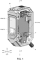
- FIG. 1 is a perspective view showing a photosensor 1 according to an embodiment of the disclosure.
- the photosensor 1 is configured as a retroreflective photoelectric sensor, is built-in with a light projecting part 11, a light receiving part 12, an amplification part 13, a control part 14, etc., and is connected to an external power source or an external device via a cable 5 penetrating through a housing 2.
- the photosensor 1 may also be configured as a transmissive photoelectric sensor and house the light projecting part 11 and the light receiving part 12 respectively in separate housings 2 and 2.
- the photosensor 1 may also be configured as an amplifier-separated photoelectric sensor with the amplification part 13 separated outside the housing 2, or may also be configured as a built-in power supply photoelectric sensor with a power supply part built in the housing 2.
- the housing 2 is formed of a metal material such as stainless steel or zinc die casting, except for window parts 11W and 12W at which the light projecting 11 and the light receiving part 12 are provided.
- the material of the housing 2 is not limited to the metal material.
- the housing 2 may also be formed of a resin material such as polybutylene terephthalate resin or ABS resin.
- the window parts 11W and 12W are formed of a light-transmitting material such as methacrylic resin or glass.
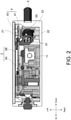
- FIG. 2 is a cross-sectional view taken along line II-II in FIG. 1 .
- the housing 2 includes a case body 20 formed in a substantially rectangular parallelepiped cup shape, and a lid 21 covering the opening of the case body 20.
- the case body 20 includes a bottom wall 22 and a peripheral wall 23 that extends up from the bottom wall 22 toward the lid 21.
- the bottom wall 22 is located on the opposite side of the lid 21.
- a substantially circular through-hole 24 is formed in the peripheral wall 23.
- the through-hole 24 may also be formed on the bottom wall 22.
- the cable 5 is inserted through the through-hole 24.
- the cable 5 has a plurality of strands 51 and an outer jacket 52 for bundling the plurality of strands 51.
- the strand 51 has a core wire composed of a plurality of conductive wires and an inner jacket covering the core wire.
- the outer jacket 52 is formed in a cylindrical shape having substantially the same diameter as the through-hole 24.
- the through-hole 24 may also be substantially oval. In that case, the outer jacket 52 may also have a tubular shape having a substantially oval cross section.
- the first circuit board 3 is housed in the housing 2.
- the size of the first circuit board 3 becomes large in order to perform complex processing.
- the first circuit board 3 may be divided to be a size equal to or smaller than a size that can be housed in the housing 2.
- the first circuit board 3 is divided into two parts including a first A circuit board 3A and a first B circuit board 3B. Although not shown, the first circuit board 3 may also be divided into three or more parts.
- the first A circuit board 3A is arranged along the lid 21 of the housing 2.
- the first B circuit board 3B is arranged along the first A circuit board 3A.
- the first circuit board 3 (the first A and first B circuit boards 3A and 3B) may also be arranged along the bottom wall 22.
- FIG. 3 is an enlarged perspective view showing the vicinity of the through-hole 24.
- electronic components and a first connector 34 are mounted on a printed wiring board of a rigid board on which a wiring pattern such as copper foil is printed on a base material in which glass fiber is impregnated with epoxy resin or the like.
- the electronic components may be mounted on two surfaces of the printed wiring board or may be mounted on one surface only.
- the electronic components mounted on the first circuit board 3 constitute, for example, the amplification part 13 and the control part 14 described above.
- the photosensor 1 of this embodiment includes a second circuit board 4 that electrically and mechanically connects the first circuit board 3 and the cable 5.
- a part of the printed wiring board of the second circuit board 4 is a flexible board on which a wiring pattern such as copper foil is printed on a film such as polyimide resin, and may be greatly elastically deformed.
- the printed wiring board of the second circuit board 4 is all composed of a flexible board.
- the printed wiring board constituting the second circuit board 4 may also be a flex-rigid board combining a flexible board and a rigid board.
- the second circuit board 4 has a first portion 41, a second portion 42, and a third portion 43 connecting the first portion 41 and the second portion 42.
- the first portion 41 is located at a first end part at one end of the second circuit board 4 and its vicinity
- the second portion 42 is located at a second end part at another end of the second circuit board 4 and its vicinity.
- the positions of the first portion 41 and the second portion 42 are not limited to the two end parts of the second circuit board 4.
- the first portion 41 and the second portion 42 may also be located between the first end part and the second end part.
- the first portion 41 is composed of a flexible board and is formed in such a size that it cannot pass through the through-hole 24 in a non-elastically deformed state but can pass through the through-hole 24 in an elastically deformed state. Specifically, it is formed to have a width larger than the diameter of the through-hole 24 excluding a recess 25 to be described later.
- Each strand 51 of the cable 5 is soldered to the wiring pattern of the first portion 41 to be electrically and mechanically connected.
- the second portion 42 is provided with a second connector 44 that can be inserted into and removed from the first connector 34. The second connector 44 is inserted into the first connector 34 to be electrically and mechanically connected.
- FIG. 4 is a perspective view showing a state before the second circuit board 4 is inserted into the through-hole 24 and arranged in the housing 2.
- FIG. 5 is a perspective view showing a state after the second circuit board 4 is inserted into the through-hole 24 and arranged in the housing 2. As shown in FIG. 5 , the cable 5 is fixed to the housing 2 at the edge of the through-hole 24.
- the cable 5 is provided with a protrusion 55 protruding from the outer jacket 52.
- a flange part 56 that spreads radially from the outer jacket 52 is provided on the opposite side of the protrusion 55 with the portion to be inserted through the through-hole 24 interposed therebetween.
- the flange part 56 may be provided with a packing for dustproofing and waterproofing.
- a recess (notch) 25 is formed at a position corresponding to the protrusion 55.
- the cable 5 may be fixed to the housing 2 (see FIG. 5 ).
- the protrusion 55 and the flange part 56 may be externally attached to the outer jacket 52 or may be integrally formed.
- FIG. 6 is a view showing an example of a process of manufacturing the photosensor 1.
- a first circuit board is housed in a housing 2 (step S1).
- the first circuit board 3 is provided with a first connector 34.
- a through-hole 24 is formed in the housing 2.
- strands 51 of a cable 5 are soldered to a wiring pattern of a second circuit board 4 to electrically and mechanically connect the second circuit board 4 and the cable 5 (step S2). Steps S1 and S2 may be performed in a reverse order.
- the second circuit board 4 with the cable 5 soldered is inserted from the through-hole 24 and arranged in the housing 2 (step S3).
- the cable 5 may be fixed to the housing 2 as described with reference to FIG. 4 and FIG. 5 .
- a second connector 44 is inserted into the first connector 34 to electrically and mechanically connect the first circuit board 3 and the second circuit board 4 (step S4). Accordingly, the cable 5 is electrically connected to the first circuit board 3.
- the cable can be easily mounted on the first circuit board via the second circuit board. As shown in FIG. 6 , in the housing 2, it is only necessary to insert the second connector 44 into the first connector 34. Since the cable 5 is soldered outside the housing 2 and connected in advance to the second circuit board 4, soldering inside the housing 2 can be omitted.
- the cable 5 is fixed to the housing 2 at the edge of the through-hole 24.
- the cable 5 is fixed to the housing 2 even if the cable 5 is pulled from the outside, the load is less likely to be applied to the connected portion at which the cable 5 is soldered.
- the assembly of the photosensor 1 since the cable 5 is fixed to the housing 2 and cannot be moved freely, it becomes difficult to solder the cable 5 to the circuit board.
- the housing 2 can be compactly configured by omitting the space for housing the extended cable 5.
- At least a part of the printed wiring board of the second circuit board 4 is composed of a flexible board instead of a rigid board. Since the second circuit board 4 may be elastically deformed, it is easy to insert the second connector 44 into the first connector 34 in the assembly of the photosensor 1. The second circuit board 4 with the cable 5 connected can be easily mounted on the first circuit board 3.
- the printed wiring board of the second circuit board 4 is all a flexible board, it may also be a flex-rigid board combining a flexible board and a rigid board.
- the first portion 41 of the second circuit board 4 is formed in a size that cannot pass through the through-hole 24 unless it is elastically deformed. Since a large mounting area partitioned in the first portion 41 can be secured, the cable 5 can be easily soldered to the second circuit board 4, and the connection reliability between the second circuit board 4 and the cable 5 can be improved.
- a photosensor (1) including:
- a method of manufacturing a photosensor (1) including:
Landscapes
- Engineering & Computer Science (AREA)
- Microelectronics & Electronic Packaging (AREA)
- Manufacturing & Machinery (AREA)
- Physics & Mathematics (AREA)
- General Physics & Mathematics (AREA)
- Spectroscopy & Molecular Physics (AREA)
- Insertion, Bundling And Securing Of Wires For Electric Apparatuses (AREA)
- Optical Transform (AREA)
- Switches Operated By Changes In Physical Conditions (AREA)
Abstract
Description
- The disclosure relates to a photosensor.
- In a photosensor such as a photoelectric sensor or an image sensor, a circuit board that constitutes a control part or the like is built in a housing. A cable penetrates through the housing and is connected to the circuit board in order to supply power from outside the housing to the circuit board and transmit a signal processed by the circuit board to outside of the housing.
-
- [Patent Document 1]
Japanese Patent Application Laid-Open No. 2004-257857 - [Patent Document 2]
Japanese Patent Application Laid-Open No. 2007-3348 - For example,
FIG. 3 ofPatent Document 1 andFIG. 2 ofPatent Document 2 disclose a configuration in which the tip of a cable inserted into a housing is soldered to a circuit board. In the assembly of the photosensor, the work of soldering and mounting the cable to the circuit board is a heavy burden on the operator. In particular, if the cable is fixed to the housing, since the tip of the cable cannot be moved freely, the mounting work becomes difficult. - In
Patent Documents - Therefore, an objective of the disclosure is to provide a photosensor in which a cable can be easily mounted on a circuit board.
- A photosensor according to an embodiment of the disclosure includes a housing, a cable, a first circuit board, and a second circuit board. A through-hole is formed in the housing. The cable is inserted through the through-hole. The first circuit board and the second circuit board are housed in the
housing 2. The first circuit board is provided with a first connector. The second circuit board has a first portion and a second portion. The cable is soldered to the first portion. The first portion is provided with a second connector. The second connector is inserted into the first connector. The second circuit board connects the cable and the first circuit board. - A method of manufacturing a photosensor according to an embodiment of the disclosure includes a step of housing a first circuit board in a housing, a step of soldering a cable to a second circuit board to connect the second circuit board and cable, a step of inserting from a through-hole the second circuit board soldered with the cable and arranging in the housing, and a step of inserting a second connector into a first connector to connect the first circuit board and the second circuit board. The through-hole is formed in the housing. The first circuit board is provided with the first connector. The second circuit board is provided with the second connector that may be inserted into and removed from the first connector.
- According to these embodiments, the cable can be easily mounted on the first circuit board via the second circuit board. In the housing, the second connector may be simply inserted into the first connector. Since the cable is soldered in advance outside the housing and connected to the second circuit board, soldering inside the housing can be omitted. Since it is not necessary to extend the tip of the cable and solder it, the housing can be compactly configured by omitting the space for housing the extended cable.
- In the above embodiment, it is preferable that at least a part of the printed wiring board of the second circuit board is composed of a flexible board instead of a rigid board. The printed wiring board of the second circuit board may all be a flexible board, or may be a flex-rigid board combining a flexible board and a rigid board.
- According to this embodiment, since the second circuit board can be elastically deformed, it is easy to insert the second connector into the first connector. The second circuit board with the cable connected can be easily mounted on the first circuit board.
- In the above embodiment, the first portion may be composed of a flexible board and may be formed in a size incapable of passing through the through-hole in a non-elastically deformed state but capable of passing through the through-hole in an elastically deformed state.
- According to this embodiment, since the first portion may be elastically deformed, even if the first portion is larger than the through-hole, it can be passed through the through-hole. Since a large area partitioned in the first portion for soldering the cable can be secured, it is easy to solder the cable to the second circuit board. The connection reliability between the second circuit board and the cable can be improved. If the gap between the strands is too narrow, solder may flow to the adjacent strand and cause a short circuit, or a high-temperature soldering iron may come into contact with the adjacent strand and cause damage.
- In the above embodiment, the cable may be fixed to the housing at an edge of the through-hole.
- When the cable is fixed to the housing at the portion penetrating through the housing, even if the cable is pulled from the outside, a load is less likely to be applied to the connected portion at which the cable is soldered. In contrast, in the assembly of the photosensor, since the cable is fixed to the housing and cannot be moved freely, it becomes difficult to solder the cable to the circuit board. However, according to this embodiment, the work of soldering the cable to the circuit board can be omitted. Even a cable fixed to the housing can be easily mounted on the circuit board.
- According to the disclosure, it is possible to provide a photosensor in which a cable can be easily mounted on a circuit board.
-
-
FIG. 1 is a perspective view showing a photosensor according to an embodiment of the disclosure. -
FIG. 2 is a cross-sectional view taken along line II-II inFIG. 1 . -
FIG. 3 is an enlarged perspective view showing the vicinity of a through-hole shown inFIG. 1 . -
FIG. 4 is a perspective view showing a state before a second circuit board is inserted into the through-hole and arranged in the housing. -
FIG. 5 is a perspective view showing a state after the second circuit board is inserted into the through-hole and arranged in the housing. -
FIG. 6 is a view showing an example of a process of manufacturing the photosensor according to an embodiment of the disclosure. - Preferred embodiments of the disclosure will be described with reference to the accompanying drawings. In the drawings, parts labeled with the same reference numerals have the same or similar configurations. In
FIG. 1 to FIG. 6 , as an example of aphotosensor 1, a photoelectric sensor including a light projecting part that emits light and a light receiving part that receives light is disclosed. The amount of light that reaches the light receiving part changes as the projected light is blocked or reflected by a workpiece. The photoelectric sensor may detect this change, convert it into an electric signal, and output it to an external device. - However, the
photosensor 1 is not limited to the photoelectric sensor. Thephotosensor 1 may be a displacement sensor that measures a distance from the sensor to an object by detecting a physical change amount of the object with an optical element and calculating the change amount into a distance, thephotosensor 1 may also be an image sensor that calculates an area, a center of gravity, a length, a position, etc. of an object by image processing an image captured by a camera and outputs a data and a determination result, or thephotosensor 1 may also be a code reader that reads a barcode or a two-dimensional code. - In the
photosensor 1 according to an embodiment of the disclosure, acable 5 for supplying power from an external power source to afirst circuit board 3 and transmitting a signal processed by thefirst circuit board 3 to an external device is not soldered to thefirst circuit board 3. Thecable 5 is soldered to asecond circuit board 4 and is connected to thefirst circuit board 3 via thesecond circuit board 4. - The
first circuit board 3 is composed of a printed wiring board of a rigid board that may be mounted at a high density; in contrast, thesecond circuit board 4 is composed of a printed wiring board of a flexible board that may be greatly elastically deformed. Thecable 5 may be mounted on thefirst circuit board 3 simply by inserting asecond connector 44 provided on thesecond circuit board 4 into afirst connector 34 provided on thefirst circuit board 3. Hereinafter, each configuration will be described in detail with reference toFIG. 1 to FIG. 6 . -
FIG. 1 is a perspective view showing aphotosensor 1 according to an embodiment of the disclosure. In the illustrated example, thephotosensor 1 is configured as a retroreflective photoelectric sensor, is built-in with alight projecting part 11, alight receiving part 12, an amplification part 13, a control part 14, etc., and is connected to an external power source or an external device via acable 5 penetrating through ahousing 2. Thephotosensor 1 may also be configured as a transmissive photoelectric sensor and house thelight projecting part 11 and thelight receiving part 12 respectively inseparate housings photosensor 1 may also be configured as an amplifier-separated photoelectric sensor with the amplification part 13 separated outside thehousing 2, or may also be configured as a built-in power supply photoelectric sensor with a power supply part built in thehousing 2. - The
housing 2 is formed of a metal material such as stainless steel or zinc die casting, except forwindow parts light receiving part 12 are provided. However, the material of thehousing 2 is not limited to the metal material. For example, thehousing 2 may also be formed of a resin material such as polybutylene terephthalate resin or ABS resin. Thewindow parts -
FIG. 2 is a cross-sectional view taken along line II-II inFIG. 1 . As shown inFIG. 2 , thehousing 2 includes a case body 20 formed in a substantially rectangular parallelepiped cup shape, and alid 21 covering the opening of the case body 20. The case body 20 includes abottom wall 22 and aperipheral wall 23 that extends up from thebottom wall 22 toward thelid 21. In thehousing 2, thebottom wall 22 is located on the opposite side of thelid 21. - In the illustrated example, a substantially circular through-
hole 24 is formed in theperipheral wall 23. The through-hole 24 may also be formed on thebottom wall 22. Thecable 5 is inserted through the through-hole 24. Thecable 5 has a plurality ofstrands 51 and anouter jacket 52 for bundling the plurality ofstrands 51. Thestrand 51 has a core wire composed of a plurality of conductive wires and an inner jacket covering the core wire. Theouter jacket 52 is formed in a cylindrical shape having substantially the same diameter as the through-hole 24. The through-hole 24 may also be substantially oval. In that case, theouter jacket 52 may also have a tubular shape having a substantially oval cross section. - The
first circuit board 3 is housed in thehousing 2. When a high-performance photosensor 1 capable of detecting various workpieces is configured, the size of thefirst circuit board 3 becomes large in order to perform complex processing. Instead of increasing the size of thehousing 2 according to thefirst circuit board 3, thefirst circuit board 3 may be divided to be a size equal to or smaller than a size that can be housed in thehousing 2. - In the illustrated example, the
first circuit board 3 is divided into two parts including a firstA circuit board 3A and a firstB circuit board 3B. Although not shown, thefirst circuit board 3 may also be divided into three or more parts. The firstA circuit board 3A is arranged along thelid 21 of thehousing 2. The firstB circuit board 3B is arranged along the firstA circuit board 3A. The first circuit board 3 (the first A and firstB circuit boards bottom wall 22. -
FIG. 3 is an enlarged perspective view showing the vicinity of the through-hole 24. As shown inFIG. 3 , in thefirst circuit board 3, electronic components and afirst connector 34 are mounted on a printed wiring board of a rigid board on which a wiring pattern such as copper foil is printed on a base material in which glass fiber is impregnated with epoxy resin or the like. The electronic components may be mounted on two surfaces of the printed wiring board or may be mounted on one surface only. The electronic components mounted on thefirst circuit board 3 constitute, for example, the amplification part 13 and the control part 14 described above. - One of the features of the
photosensor 1 of this embodiment is that it includes asecond circuit board 4 that electrically and mechanically connects thefirst circuit board 3 and thecable 5. At least a part of the printed wiring board of thesecond circuit board 4 is a flexible board on which a wiring pattern such as copper foil is printed on a film such as polyimide resin, and may be greatly elastically deformed. In the illustrated example, the printed wiring board of thesecond circuit board 4 is all composed of a flexible board. The printed wiring board constituting thesecond circuit board 4 may also be a flex-rigid board combining a flexible board and a rigid board. - The
second circuit board 4 has afirst portion 41, asecond portion 42, and athird portion 43 connecting thefirst portion 41 and thesecond portion 42. In the illustrated example, thefirst portion 41 is located at a first end part at one end of thesecond circuit board 4 and its vicinity, and thesecond portion 42 is located at a second end part at another end of thesecond circuit board 4 and its vicinity. The positions of thefirst portion 41 and thesecond portion 42 are not limited to the two end parts of thesecond circuit board 4. Thefirst portion 41 and thesecond portion 42 may also be located between the first end part and the second end part. - The
first portion 41 is composed of a flexible board and is formed in such a size that it cannot pass through the through-hole 24 in a non-elastically deformed state but can pass through the through-hole 24 in an elastically deformed state. Specifically, it is formed to have a width larger than the diameter of the through-hole 24 excluding arecess 25 to be described later. Eachstrand 51 of thecable 5 is soldered to the wiring pattern of thefirst portion 41 to be electrically and mechanically connected. Thesecond portion 42 is provided with asecond connector 44 that can be inserted into and removed from thefirst connector 34. Thesecond connector 44 is inserted into thefirst connector 34 to be electrically and mechanically connected. - Next, a process of manufacturing the
photosensor 1 will be described with reference toFIG. 4 to FIG. 6 .FIG. 4 is a perspective view showing a state before thesecond circuit board 4 is inserted into the through-hole 24 and arranged in thehousing 2.FIG. 5 is a perspective view showing a state after thesecond circuit board 4 is inserted into the through-hole 24 and arranged in thehousing 2. As shown inFIG. 5 , thecable 5 is fixed to thehousing 2 at the edge of the through-hole 24. - As shown in
FIG. 4 , thecable 5 is provided with aprotrusion 55 protruding from theouter jacket 52. Aflange part 56 that spreads radially from theouter jacket 52 is provided on the opposite side of theprotrusion 55 with the portion to be inserted through the through-hole 24 interposed therebetween. Theflange part 56 may be provided with a packing for dustproofing and waterproofing. In the through-hole 24, a recess (notch) 25 is formed at a position corresponding to theprotrusion 55. When theprotrusion 55 is passed through therecess 25 and rotated by 90° (seeFIG. 4 ), thecable 5 may be fixed to the housing 2 (seeFIG. 5 ). Theprotrusion 55 and theflange part 56 may be externally attached to theouter jacket 52 or may be integrally formed. -
FIG. 6 is a view showing an example of a process of manufacturing thephotosensor 1. To manufacture thephotosensor 1, a first circuit board is housed in a housing 2 (step S1). Thefirst circuit board 3 is provided with afirst connector 34. A through-hole 24 is formed in thehousing 2. Next,strands 51 of acable 5 are soldered to a wiring pattern of asecond circuit board 4 to electrically and mechanically connect thesecond circuit board 4 and the cable 5 (step S2). Steps S1 and S2 may be performed in a reverse order. - Next, the
second circuit board 4 with thecable 5 soldered is inserted from the through-hole 24 and arranged in the housing 2 (step S3). At this time, thecable 5 may be fixed to thehousing 2 as described with reference toFIG. 4 andFIG. 5 . Next, asecond connector 44 is inserted into thefirst connector 34 to electrically and mechanically connect thefirst circuit board 3 and the second circuit board 4 (step S4). Accordingly, thecable 5 is electrically connected to thefirst circuit board 3. - According to the
photosensor 1 of this embodiment configured as described above, the cable can be easily mounted on the first circuit board via the second circuit board. As shown inFIG. 6 , in thehousing 2, it is only necessary to insert thesecond connector 44 into thefirst connector 34. Since thecable 5 is soldered outside thehousing 2 and connected in advance to thesecond circuit board 4, soldering inside thehousing 2 can be omitted. - As shown in
FIG. 3 , thecable 5 is fixed to thehousing 2 at the edge of the through-hole 24. When thecable 5 is fixed to thehousing 2, even if thecable 5 is pulled from the outside, the load is less likely to be applied to the connected portion at which thecable 5 is soldered. In contrast, in the assembly of thephotosensor 1, since thecable 5 is fixed to thehousing 2 and cannot be moved freely, it becomes difficult to solder thecable 5 to the circuit board. - According to this embodiment, since the work of soldering the
cable 5 to thefirst circuit board 3 can be omitted, even acable 5 fixed to thehousing 2 can be easily mounted on thefirst circuit board 3. Since it is not necessary to extend the tip of thecable 5 and solder it, as shown inFIG. 1 andFIG. 2 , thehousing 2 can be compactly configured by omitting the space for housing theextended cable 5. - At least a part of the printed wiring board of the
second circuit board 4 is composed of a flexible board instead of a rigid board. Since thesecond circuit board 4 may be elastically deformed, it is easy to insert thesecond connector 44 into thefirst connector 34 in the assembly of thephotosensor 1. Thesecond circuit board 4 with thecable 5 connected can be easily mounted on thefirst circuit board 3. In the example shown inFIG. 3 , although the printed wiring board of thesecond circuit board 4 is all a flexible board, it may also be a flex-rigid board combining a flexible board and a rigid board. - As shown in
FIG. 4 andFIG. 5 , thefirst portion 41 of thesecond circuit board 4 is formed in a size that cannot pass through the through-hole 24 unless it is elastically deformed. Since a large mounting area partitioned in thefirst portion 41 can be secured, thecable 5 can be easily soldered to thesecond circuit board 4, and the connection reliability between thesecond circuit board 4 and thecable 5 can be improved. - The embodiments described above are intended to facilitate the understanding of the disclosure and are not intended to limit the interpretation the disclosure. Each element included in the embodiments and its arrangement, material, condition, shape, size, etc. are not limited to those exemplified herein and may be changed as appropriate. In addition, the configurations shown in different embodiments may be partially replaced or combined.
- A photosensor (1) including:
- a housing (2) in which a through-hole (24) is formed;
- a cable (5) inserted through the through-hole (24);
- a first circuit board (3) housed in the housing (2) and provided with a first connector (34); and
- a second circuit board (4) connecting the cable (5) and the first circuit board (3),
- where the second circuit board (4) has a first portion (41) to which the cable (5) is soldered, and a second portion (42) provided with a second connector (44) inserted into the first connector (34).
- A method of manufacturing a photosensor (1), including:
- a step (S1) of housing a first circuit board (3) provided with a first connector (34) in a housing (2) in which a through-hole (24) is formed;
- a step (S2) of soldering a cable (5) to a second circuit board (4) provided with a second connector (44) capable of being inserted into and removed from the first connector (34) to connect the second circuit board (4) and the cable (5);
- a step (S3) of inserting from the through-hole (24) the second circuit board (4) soldered with the cable (5) and arranging in the housing (2); and
- a step (S4) of inserting the second connector (44) into the first connector (34) to connect the first circuit board (3) and the second circuit board (4).
-
- 1
- photosensor
- 2
- housing
- 3
- first circuit board
- 3A
- first A circuit board
- 3B
- first B circuit board
- 4
- second circuit board
- 5
- cable
- 11
- light projecting part
- 12
- light receiving part
- 11W, 12W
- window part
- 13
- amplification part
- 14
- control part
- 20
- case body
- 21
- lid
- 22
- bottom wall
- 23
- peripheral wall
- 24
- through-hole
- 25
- recess
- 34
- first connector
- 41
- first portion
- 42
- second portion
- 43
- third portion
- 44
- second connector
- 51
- strand
- 52
- outer jacket
- 55
- protrusion
- 56
- flange part
Claims (5)
- A photosensor comprising:a housing in which a through-hole is formed;a cable inserted through the through-hole;a first circuit board housed in the housing and provided with a first connector; anda second circuit board connecting the cable and the first circuit board,wherein the second circuit board has a first portion to which the cable is soldered, and a second portion provided with a second connector inserted into the first connector.
- The photosensor according to claim 1, wherein at least a part of the second circuit board is composed of a flexible board.
- The photosensor according to claim 2, wherein the first portion is composed of a flexible board and is formed in a size incapable of passing through the through-hole in a non-elastically deformed state but capable of passing through the through-hole in an elastically deformed state.
- The photosensor according to any one of claims 1 to 3, wherein the cable is fixed to the housing at an edge of the through-hole.
- A method of manufacturing a photosensor, comprising:a step of housing a first circuit board provided with a first connector in a housing in which a through-hole is formed;a step of soldering a cable to a second circuit board provided with a second connector capable of being inserted into and removed from the first connector to connect the second circuit board and the cable;a step of inserting from the through-hole the second circuit board soldered with the cable and arranging in the housing; anda step of inserting the second connector into the first connector to connect the first circuit board and the second circuit board.
Applications Claiming Priority (2)
| Application Number | Priority Date | Filing Date | Title |
|---|---|---|---|
| JP2019048468A JP7153237B2 (en) | 2019-03-15 | 2019-03-15 | light sensor |
| PCT/JP2020/010316 WO2020189416A1 (en) | 2019-03-15 | 2020-03-10 | Photosensor |
Publications (2)
| Publication Number | Publication Date |
|---|---|
| EP3941169A1 true EP3941169A1 (en) | 2022-01-19 |
| EP3941169A4 EP3941169A4 (en) | 2022-12-14 |
Family
ID=72432171
Family Applications (1)
| Application Number | Title | Priority Date | Filing Date |
|---|---|---|---|
| EP20774625.6A Withdrawn EP3941169A4 (en) | 2019-03-15 | 2020-03-10 | PHOTOSENSOR |
Country Status (6)
| Country | Link |
|---|---|
| US (1) | US11744025B2 (en) |
| EP (1) | EP3941169A4 (en) |
| JP (1) | JP7153237B2 (en) |
| KR (1) | KR102723459B1 (en) |
| CN (1) | CN113439491B (en) |
| WO (1) | WO2020189416A1 (en) |
Family Cites Families (23)
| Publication number | Priority date | Publication date | Assignee | Title |
|---|---|---|---|---|
| JPS5794992U (en) * | 1980-12-01 | 1982-06-11 | ||
| JPS5794992A (en) | 1980-12-02 | 1982-06-12 | Fujitsu Ltd | Address-over check system of memory device |
| JPH0837351A (en) * | 1994-07-21 | 1996-02-06 | Amp Japan Ltd | Flexible circuit board harness device and flexible circuit board used therefor |
| DE4434011C1 (en) | 1994-09-23 | 1995-07-20 | Leuze Electronic Gmbh & Co | Optoelectronic device |
| DE19820358C1 (en) * | 1998-05-07 | 1999-08-05 | Leuze Electronic Gmbh & Co | Optoelectronics sensor, esp. for use as a light barrier or light sensor |
| JP3736536B2 (en) | 2003-02-26 | 2006-01-18 | オムロン株式会社 | Photoelectric sensor |
| US7297017B2 (en) * | 2004-12-16 | 2007-11-20 | Giga-Byte Technology Co., Ltd. | Method for safely removing connecting device of peripheral equipment of computer |
| JP2007003348A (en) | 2005-06-23 | 2007-01-11 | Omron Corp | Regression reflection typed photo-electronic sensor |
| JP2007053144A (en) * | 2005-08-15 | 2007-03-01 | Fujifilm Corp | Electronic apparatus and photographing apparatus |
| JP2007299784A (en) * | 2006-04-27 | 2007-11-15 | Toshiba Corp | Mounting structure and electronic device having mounting structure |
| JP2011192794A (en) * | 2010-03-15 | 2011-09-29 | Yamatake Corp | Cable lead-out structure |
| JP2012088571A (en) * | 2010-10-20 | 2012-05-10 | Fujikura Ltd | Optoelectric composite connector and cable with connector |
| DE102011015816B4 (en) * | 2011-04-01 | 2017-09-21 | Yamaichi Electronics Deutschland Gmbh | Plug and plug connector assembly |
| TWM416814U (en) * | 2011-05-05 | 2011-11-21 | Mastouch Optoelectronics Technologies Co Ltd | Touch panel and touch control electronic device with photoelectric conversion capability |
| CN104181653B (en) * | 2013-05-23 | 2016-03-23 | 富士康(昆山)电脑接插件有限公司 | Cable Connector Assembly |
| US10410760B2 (en) * | 2016-01-11 | 2019-09-10 | Raytheon Company | Rigid-flex assembly for high-speed sensor module comprising a flexible wiring section with dual flexible strips stacked and attached together |
| JP2017135349A (en) * | 2016-01-29 | 2017-08-03 | 富士通株式会社 | Electronic apparatus |
| JP2017157760A (en) * | 2016-03-03 | 2017-09-07 | オムロン株式会社 | Optical electronics |
| JP6873608B2 (en) * | 2016-06-02 | 2021-05-19 | 日本電産サンキョー株式会社 | Optical unit with runout correction function |
| CN109983852B (en) * | 2016-11-17 | 2022-02-01 | 住友电工印刷电路株式会社 | Method for manufacturing flexible printed wiring board and apparatus for manufacturing flexible printed wiring board |
| JP2018137174A (en) * | 2017-02-23 | 2018-08-30 | オムロン株式会社 | Electronics |
| KR20180113393A (en) * | 2017-04-06 | 2018-10-16 | 주식회사 엠씨넥스 | Method of manufacturing cable assembly for camera, and cable assembly for camera thereby |
| CN109831086A (en) * | 2019-02-20 | 2019-05-31 | 东莞盛翔精密金属有限公司 | A kind of linear vibration motor with U-shaped coil and U-shaped permanent magnet |
-
2019
- 2019-03-15 JP JP2019048468A patent/JP7153237B2/en active Active
-
2020
- 2020-03-10 US US17/432,101 patent/US11744025B2/en active Active
- 2020-03-10 WO PCT/JP2020/010316 patent/WO2020189416A1/en not_active Ceased
- 2020-03-10 CN CN202080014902.4A patent/CN113439491B/en active Active
- 2020-03-10 EP EP20774625.6A patent/EP3941169A4/en not_active Withdrawn
- 2020-03-10 KR KR1020217025077A patent/KR102723459B1/en active Active
Also Published As
| Publication number | Publication date |
|---|---|
| EP3941169A4 (en) | 2022-12-14 |
| US11744025B2 (en) | 2023-08-29 |
| WO2020189416A1 (en) | 2020-09-24 |
| KR20210111834A (en) | 2021-09-13 |
| CN113439491B (en) | 2022-07-08 |
| US20220201875A1 (en) | 2022-06-23 |
| JP7153237B2 (en) | 2022-10-14 |
| JP2020150205A (en) | 2020-09-17 |
| KR102723459B1 (en) | 2024-10-29 |
| CN113439491A (en) | 2021-09-24 |
Similar Documents
| Publication | Publication Date | Title |
|---|---|---|
| US11689795B2 (en) | Vehicular camera with stacked circuit boards and metallic connecting element | |
| KR101128931B1 (en) | Camera module | |
| US9571202B2 (en) | Optical connector assembly | |
| US6739907B2 (en) | Coaxial connector contact and coaxial connector having it | |
| US10574866B2 (en) | Imaging unit and endoscope apparatus | |
| US20200060514A1 (en) | Endoscope and method of manufacturing endoscope | |
| US11744025B2 (en) | Photosensor comprising a first circuit board within a housing having a through hole with a cable for connecting a second circuit board and method of manufacturing the same | |
| US12082784B2 (en) | Electronic module, method of manufacturing electronic module, and endoscope | |
| JP2005116400A (en) | Optical active connector | |
| JP6695366B2 (en) | Imaging module | |
| KR102316121B1 (en) | Connectors and Electronics Systems | |
| JP7511815B2 (en) | Optical Sensor | |
| CN211700274U (en) | Light sensing switch structure | |
| CN104833379A (en) | Detector and method of producing of detector | |
| JP2016201436A (en) | Housing structure of electronic device | |
| JP2006344571A (en) | Electrical equipment | |
| JP2005333236A (en) | Antenna device with circuit | |
| JP2017129504A (en) | Moving body detector | |
| JP2018087741A (en) | Moving object detection apparatus | |
| JP2007323974A (en) | Sensor device and manufacturing method thereof | |
| JP2008123099A (en) | Vein pattern acquisition device | |
| KR20100006768U (en) | Front connector for I / O module of PL system with jumper wire coupling structure |
Legal Events
| Date | Code | Title | Description |
|---|---|---|---|
| STAA | Information on the status of an ep patent application or granted ep patent |
Free format text: STATUS: THE INTERNATIONAL PUBLICATION HAS BEEN MADE |
|
| PUAI | Public reference made under article 153(3) epc to a published international application that has entered the european phase |
Free format text: ORIGINAL CODE: 0009012 |
|
| STAA | Information on the status of an ep patent application or granted ep patent |
Free format text: STATUS: REQUEST FOR EXAMINATION WAS MADE |
|
| 17P | Request for examination filed |
Effective date: 20210817 |
|
| AK | Designated contracting states |
Kind code of ref document: A1 Designated state(s): AL AT BE BG CH CY CZ DE DK EE ES FI FR GB GR HR HU IE IS IT LI LT LU LV MC MK MT NL NO PL PT RO RS SE SI SK SM TR |
|
| DAV | Request for validation of the european patent (deleted) | ||
| DAX | Request for extension of the european patent (deleted) | ||
| REG | Reference to a national code |
Ref country code: DE Ref legal event code: R079 Free format text: PREVIOUS MAIN CLASS: H05K0007000000 Ipc: H05K0001140000 |
|
| A4 | Supplementary search report drawn up and despatched |
Effective date: 20221115 |
|
| RIC1 | Information provided on ipc code assigned before grant |
Ipc: H05K 3/36 20060101ALI20221109BHEP Ipc: H05K 3/34 20060101ALI20221109BHEP Ipc: H05K 1/14 20060101AFI20221109BHEP |
|
| STAA | Information on the status of an ep patent application or granted ep patent |
Free format text: STATUS: THE APPLICATION HAS BEEN WITHDRAWN |
|
| 18W | Application withdrawn |
Effective date: 20251121 |