EP3940956A1 - Control circuitry for power semiconductor switches using control signal feedback - Google Patents
Control circuitry for power semiconductor switches using control signal feedback Download PDFInfo
- Publication number
- EP3940956A1 EP3940956A1 EP21171047.0A EP21171047A EP3940956A1 EP 3940956 A1 EP3940956 A1 EP 3940956A1 EP 21171047 A EP21171047 A EP 21171047A EP 3940956 A1 EP3940956 A1 EP 3940956A1
- Authority
- EP
- European Patent Office
- Prior art keywords
- fet
- control
- reference voltage
- semiconductor switch
- voltage
- Prior art date
- Legal status (The legal status is an assumption and is not a legal conclusion. Google has not performed a legal analysis and makes no representation as to the accuracy of the status listed.)
- Granted
Links
Images


Classifications
-
- H—ELECTRICITY
- H03—ELECTRONIC CIRCUITRY
- H03K—PULSE TECHNIQUE
- H03K17/00—Electronic switching or gating, i.e. not by contact-making and –breaking
- H03K17/51—Electronic switching or gating, i.e. not by contact-making and –breaking characterised by the components used
- H03K17/56—Electronic switching or gating, i.e. not by contact-making and –breaking characterised by the components used by the use, as active elements, of semiconductor devices
- H03K17/687—Electronic switching or gating, i.e. not by contact-making and –breaking characterised by the components used by the use, as active elements, of semiconductor devices the devices being field-effect transistors
- H03K17/693—Switching arrangements with several input- or output-terminals, e.g. multiplexers, distributors
-
- H—ELECTRICITY
- H03—ELECTRONIC CIRCUITRY
- H03K—PULSE TECHNIQUE
- H03K17/00—Electronic switching or gating, i.e. not by contact-making and –breaking
- H03K17/14—Modifications for compensating variations of physical values, e.g. of temperature
- H03K17/145—Modifications for compensating variations of physical values, e.g. of temperature in field-effect transistor switches
-
- H—ELECTRICITY
- H03—ELECTRONIC CIRCUITRY
- H03K—PULSE TECHNIQUE
- H03K17/00—Electronic switching or gating, i.e. not by contact-making and –breaking
- H03K17/04—Modifications for accelerating switching
- H03K17/041—Modifications for accelerating switching without feedback from the output circuit to the control circuit
- H03K17/0412—Modifications for accelerating switching without feedback from the output circuit to the control circuit by measures taken in the control circuit
- H03K17/04123—Modifications for accelerating switching without feedback from the output circuit to the control circuit by measures taken in the control circuit in field-effect transistor switches
-
- H—ELECTRICITY
- H03—ELECTRONIC CIRCUITRY
- H03K—PULSE TECHNIQUE
- H03K17/00—Electronic switching or gating, i.e. not by contact-making and –breaking
- H03K17/08—Modifications for protecting switching circuit against overcurrent or overvoltage
- H03K17/082—Modifications for protecting switching circuit against overcurrent or overvoltage by feedback from the output to the control circuit
- H03K17/0822—Modifications for protecting switching circuit against overcurrent or overvoltage by feedback from the output to the control circuit in field-effect transistor switches
-
- H—ELECTRICITY
- H03—ELECTRONIC CIRCUITRY
- H03K—PULSE TECHNIQUE
- H03K17/00—Electronic switching or gating, i.e. not by contact-making and –breaking
- H03K17/10—Modifications for increasing the maximum permissible switched voltage
- H03K17/102—Modifications for increasing the maximum permissible switched voltage in field-effect transistor switches
-
- H—ELECTRICITY
- H03—ELECTRONIC CIRCUITRY
- H03K—PULSE TECHNIQUE
- H03K17/00—Electronic switching or gating, i.e. not by contact-making and –breaking
- H03K17/22—Modifications for ensuring a predetermined initial state when the supply voltage has been applied
- H03K17/223—Modifications for ensuring a predetermined initial state when the supply voltage has been applied in field-effect transistor switches
-
- H—ELECTRICITY
- H10—SEMICONDUCTOR DEVICES; ELECTRIC SOLID-STATE DEVICES NOT OTHERWISE PROVIDED FOR
- H10D—INORGANIC ELECTRIC SEMICONDUCTOR DEVICES
- H10D62/00—Semiconductor bodies, or regions thereof, of devices having potential barriers
- H10D62/80—Semiconductor bodies, or regions thereof, of devices having potential barriers characterised by the materials
- H10D62/83—Semiconductor bodies, or regions thereof, of devices having potential barriers characterised by the materials being Group IV materials, e.g. B-doped Si or undoped Ge
- H10D62/832—Semiconductor bodies, or regions thereof, of devices having potential barriers characterised by the materials being Group IV materials, e.g. B-doped Si or undoped Ge being Group IV materials comprising two or more elements, e.g. SiGe
- H10D62/8325—Silicon carbide
-
- H—ELECTRICITY
- H10—SEMICONDUCTOR DEVICES; ELECTRIC SOLID-STATE DEVICES NOT OTHERWISE PROVIDED FOR
- H10D—INORGANIC ELECTRIC SEMICONDUCTOR DEVICES
- H10D62/00—Semiconductor bodies, or regions thereof, of devices having potential barriers
- H10D62/80—Semiconductor bodies, or regions thereof, of devices having potential barriers characterised by the materials
- H10D62/85—Semiconductor bodies, or regions thereof, of devices having potential barriers characterised by the materials being Group III-V materials, e.g. GaAs
- H10D62/8503—Nitride Group III-V materials, e.g. AlN or GaN
Definitions
- the inventive subject matter relates to electrical power apparatus and methods and, more particularly, to driver circuits for power semiconductor switches.
- Insulation switches such as insulated gate bipolar transistors (IGBTs) and power metal-oxide-semiconductor field-effect transistors (MOSFETs)
- IGBTs insulated gate bipolar transistors
- MOSFETs power metal-oxide-semiconductor field-effect transistors
- IGBTs insulated gate bipolar transistors
- MOSFETs power metal-oxide-semiconductor field-effect transistors
- an apparatus includes a power semiconductor switch, a driver circuit configured to drive a control terminal of the power semiconductor switch, and a control circuit configured to apply a control signal to the driver circuit responsive to a comparison of a reference voltage to a voltage at the control terminal of the semiconductor switch.
- the power semiconductor switch may include a field effect transistor (FET), such as a wide bandgap silicon carbide (SiC) MOSFET.
- FET field effect transistor
- the control terminal may include a gate terminal of the FET, and the voltage at the control terminal may include a gate voltage.
- the driver circuit may include a totem-pole circuit and the control circuit may apply the control signal to control terminals of first and second transistors of the totem-pole circuit.
- the power semiconductor switch may include a field effect transistor (FET), the control terminal may include a gate terminal of the FET, and the voltage at the control terminal may include a gate voltage of the FET.
- the FET may include a wide bandgap FET and the first and second transistors may include respective wide bandgap transistors.
- the FET may include a SiC MOSFET and the first and second transistors of the totem-pole circuit may include respective gallium nitride (GaN) transistors.
- control circuit may include a reference voltage generator configured to generate the reference voltage responsive to a drive signal and the reference voltage may conform to a reference voltage profile stored by the reference voltage generator.
- the reference voltage profile may be adjustable.
- the apparatus may further include a reference voltage profile generator configured to adjust the reference voltage profile responsive to a sensed parameter of the power semiconductor switch.
- the power semiconductor switch may include a first power semiconductor switch
- the driver circuit may include a first driver circuit
- the control circuit may include a first control circuit configured to apply a control signal to the first driver circuit responsive to a comparison of a first reference voltage to a first voltage at the control terminal of the first semiconductor switch
- the apparatus may further include a second power semiconductor switch coupled in series or in parallel with the first semiconductor switch, a second driver circuit configured to drive a control terminal of the second power semiconductor switch, and a second control circuit configured to apply a control signal to the second driver circuit responsive to a comparison of a second reference voltage to a voltage at the control terminal of the second semiconductor switch.
- a wide bandgap power transistor includes a wide bandgap power transistor, a totem-pole circuit configured to drive the wide bandgap power transistor, and a control circuit configured to apply a control signal to the totem-pole circuit responsive to a comparison of a voltage at a control terminal of the wide bandgap power transistor to a reference voltage.
- the control circuit may include a reference voltage generator configured to generate the reference voltage responsive to a drive signal and the reference voltage may conform to a reference voltage profile stored by the reference voltage generator.
- the reference voltage profile may be adjustable.
- the apparatus may further include a reference voltage profile generator configured to adjust the reference voltage profile responsive to a sensed parameter of the wide bandgap power transistor.
- an apparatus in still further embodiments, includes a wide bandgap FET and a driver circuit comprising at least one wide bandgap gate driving transistor coupled to a gate terminal of the wide bandgap FET and controlled responsive to a voltage at the gate terminal of the wide bandgap FET.
- the apparatus further includes a control circuit configured to compare a voltage at the gate terminal of the wide bandgap FET to a reference voltage and to apply a control signal to the driver circuit responsive to the comparison.
- a control signal applied to a control terminal of a semiconductor switch such as a SiC power MOSFET gate
- a control signal applied to a control terminal of a semiconductor switch may be generated based on a comparison of a voltage applied to the control terminal to a reference voltage, which may be generated from a profile that can be calibrated for the particular power transistor.
- This comparison enables producing a continuously regulated control signal to compensate for the individual characteristics of each semiconductor forcing it to behave in a predetermined manner according to the generated profile.
- operations of series and/or parallel connected power MOSFETs having slightly different device parameters can be aligned by controlling the control signals applied to the MOSFETs based on continuous gate voltage feedback.
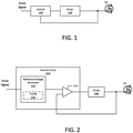
- FIG. 1 illustrates circuitry for controlling a power MOSFET Q1 according to some embodiments.
- a gate terminal of the MOSFET Q1 is driven by driver circuit 120, which may be, for example, a totem-pole or other push-pull circuit.
- a control circuit 110 applies a control signal to the driver circuit 120 responsive to a drive signal that represents a desired state of the MOSFET Q1, e.g., "on” or "off.”
- the control circuit 110 generates the control signal applied to the driver circuit 120 responsive to a comparison of a voltage at the gate terminal of the MOSFET Q1 to a reference voltage that is generated responsive to the drive signal applied to the control circuit.
- the control signal applied to the driver circuit 120 may follow a predetermined profile that provides a desired voltage waveform for the gate voltage of the MOSFET Q1.
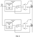
- FIG. 2 illustrates such a control circuit 210 according to further embodiments.
- the control circuit 210 includes a comparison circuit 214 (e.g., a hysteresis current regulator), which receives a reference voltage signal from a voltage reference generator circuit 212 and compares the reference voltage signal to a feedback signal corresponding to a voltage at a gate terminal of a MOSFET Q1 and regulates to the desired output on a continuous basis utilizing current regulation.
- the reference voltage signal is generated to drive a desired switch state transition for the MOSFET Q1, e.g., a transition from "on" to "off” or vice versa.
- the reference voltage may conform to a reference voltage profile 213 that corresponds to a desired dynamic behavior of the voltage applied to the gate terminal of a MOSFET Q1 driven by a driver circuit 120 for the transition commanded by the drive signal.
- the profile 213 may be implemented using, for example, an analog or digital function generator circuit which provides a desired dynamic response to the reference voltage signal applied to the comparison circuit 214 such that the gate voltage of the MOSFET Q1 exhibits a corresponding behavior in response to a state transition of the drive signal applied to the control circuit 210.
- the profile 213 may be adjustable responsive to a control input, such as a calibration input. This allows for individualized tuning of the operation of the driver circuit 120 to compensate for the particular characteristics of the MOSFET Q1 being driven.
- a reference voltage profile may be adjusted responsive to a feedback information relating to behavior of the MOSFET Q1 being driven.
- a sensor circuit 310 may detect certain real time operational parameters of the MOSFET Q1, such as on-state voltage, turn-on time, turn-off time, and the like.
- a profile generator circuit 320 may receive one or more sensor signals from the sensor circuit 310 representative of these parameters. Such information may include, for example, information indicative of turn-on and/or turn-off times of the MOSFET Q1 in relation to a timing reference.
- the voltage profile 213 of the control circuit 210 can be adjusted based on these sensed parameters to enable more precise alignment of the turn-on and/or turn-off times of the MOSFET Q1 with respect to the timing reference.
- a driver circuit used to drive a MOSFET Q1 may be a totem-pole circuit 420 that includes first and second transistors Q2, Q3 arranged in a half-bridge configuration and driven by a common control signal generated by a control circuit 210 along the lines described above with reference to FIG. 2 .
- the driver circuit transistors Q2, Q3 may be devices that are capable of significantly faster response than the speeds at which it is desired to switch the MOSFET Q1 being driven, such that the gate voltage applied to the MOSFET Q1 can be controlled as described above without the driver circuit transistors Q2, Q3 introducing undesirable delay.
- the MOSFET Q1 may be a wide bandgap MOSFET, such as a silicon carbide (SiC) MOSFET, and the transistors Q2, Q3 may be wide bandgap devices capable of operating at even higher frequencies, such as gallium nitride (GaN) transistors.
- SiC silicon carbide
- GaN gallium nitride
- the transistors Q2, Q2 of the totem-pole driver circuit 420 may be driven by a control circuit 210 that generates a control signal that drives the transistors Q2, Q3 responsive to, for example, the output of a hysteresis current regulator commanded by the comparison between a gate voltage of the MOSFET Q1 and a reference voltage regulator profile.
- the control circuit 210 includes a comparison circuit 214, which receives a voltage reference voltage signal from a reference voltage generator circuit 212.
- the reference voltage signal is generated responsive to a drive signal indicating a desired switch state transition for the MOSFET Q1, e.g., a transition from "on" to "off” or vice versa.
- the reference voltage signal conforms to a reference voltage profile 213 that identifies a desired dynamic behavior of the voltage applied to the gate terminal of a MOSFET Q1 driven by the totem-pole driver circuit 420.
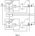
- FIG. 5 illustrates application of such control circuitry to an application in which first and second serially-connected MOSFETs Q1a, Q1b are driven in unison.
- a first control circuit 210a controls application of a control signal to a first totem-pole driver circuit 420a that drives the first MOSFET Q1a.
- a similar second control circuit 210b controls application of a control signal to a second totem-pole driver circuit 420b that drives the second MOSFET Q1b.
- first and second control circuits 210a, 210b may implement the same reference voltage profile 213 that can be set to adjust transitions of the MOSFETs Q1a, Q1b such that non-simultaneous operation may be reduced or eliminated, thus compensating, for example, for disparities in operating parameters of the first and second MOSFETs Q1a, Q1b.
- a reference voltage profile generator 520 may receive sensor feedback from sensor circuits 510a, 510b associated with respective ones of the MOSFETs Q1a, Q1b and adjust profiles 213a, 213b for reference voltage generators 212 of respective control circuits 210a, 201b responsive to the sensor feedback.
- the profile generator 520 may, for example, adjust gate drive signals applied to the MOSFETs Q1a, Q1b such that identical or nearly identical switching times can be achieved.
- a single reference voltage profile 213 may be used by respective control circuits 210a, 210b that drive respective totem-pole driver circuits 420a, 420b that drive the first and second MOSFETs Q1a, Q1b.
- the profile 213 may be adjusted such that, for example, the "on” and “off” times of the first and second MOSFETS Q1a, Q1b are substantially aligned, thus enabling reduction or elimination of current imbalances between the first and second MOSFETs Q1a, Q1b.
Landscapes
- Power Conversion In General (AREA)
- Electronic Switches (AREA)
Abstract
Description
- The inventive subject matter relates to electrical power apparatus and methods and, more particularly, to driver circuits for power semiconductor switches.
- Semiconductor switches, such as insulated gate bipolar transistors (IGBTs) and power metal-oxide-semiconductor field-effect transistors (MOSFETs), are used in a variety of different types of electrical power applications, such as in rectifiers, inverters, motor drives and the like. Solid state circuit breakers incorporating such semiconductor switches have also been developed, with the semiconductor switches being used to replace the electromechanical switches traditionally used in such devices. In such applications, semiconductor switches offer advantages of speed and resistance to environmental degradation.
- In some applications, it is desirable to have tight alignment in turn-on and turn-off of multiple semiconductor switches. For example, in operations in which power semiconductor switches are operated in series. However, disparities in characteristics of the inverter transistors, such as variances in threshold voltage and gate capacitance, can lead to variances in device turn-on and turn-off times among devices, which may cause one of the series connected semiconductor switches to carry the entire voltage. Similarly, in applications that operate multiple semiconductor switches in parallel in order to increase current carrying capacity, relatively small disparities in device parameters, such as turn-on resistance and threshold voltage, can lead to nonuniform current distribution among the paralleled devices. Such current maldistribution can lead to device overload and failure. Such problems can be particularly acute due to exceeding device capability for wide bandgap semiconductor switches, such as silicon carbide (SiC) power transistors, which may be operated at switching frequencies and/or voltage levels that are significantly greater than those used for conventional silicon devices.
- According to some embodiments, an apparatus includes a power semiconductor switch, a driver circuit configured to drive a control terminal of the power semiconductor switch, and a control circuit configured to apply a control signal to the driver circuit responsive to a comparison of a reference voltage to a voltage at the control terminal of the semiconductor switch. In some embodiments, the power semiconductor switch may include a field effect transistor (FET), such as a wide bandgap silicon carbide (SiC) MOSFET. The control terminal may include a gate terminal of the FET, and the voltage at the control terminal may include a gate voltage.
- In some embodiments, the driver circuit may include a totem-pole circuit and the control circuit may apply the control signal to control terminals of first and second transistors of the totem-pole circuit. The power semiconductor switch may include a field effect transistor (FET), the control terminal may include a gate terminal of the FET, and the voltage at the control terminal may include a gate voltage of the FET. The FET may include a wide bandgap FET and the first and second transistors may include respective wide bandgap transistors. For example, the FET may include a SiC MOSFET and the first and second transistors of the totem-pole circuit may include respective gallium nitride (GaN) transistors.
- According to further aspects, the control circuit may include a reference voltage generator configured to generate the reference voltage responsive to a drive signal and the reference voltage may conform to a reference voltage profile stored by the reference voltage generator. The reference voltage profile may be adjustable. The apparatus may further include a reference voltage profile generator configured to adjust the reference voltage profile responsive to a sensed parameter of the power semiconductor switch.
- In further embodiments, the power semiconductor switch may include a first power semiconductor switch, the driver circuit may include a first driver circuit, the control circuit may include a first control circuit configured to apply a control signal to the first driver circuit responsive to a comparison of a first reference voltage to a first voltage at the control terminal of the first semiconductor switch, and the apparatus may further include a second power semiconductor switch coupled in series or in parallel with the first semiconductor switch, a second driver circuit configured to drive a control terminal of the second power semiconductor switch, and a second control circuit configured to apply a control signal to the second driver circuit responsive to a comparison of a second reference voltage to a voltage at the control terminal of the second semiconductor switch.
- In some embodiments of the inventive subject matter, and apparatus includes a wide bandgap power transistor, a totem-pole circuit configured to drive the wide bandgap power transistor, and a control circuit configured to apply a control signal to the totem-pole circuit responsive to a comparison of a voltage at a control terminal of the wide bandgap power transistor to a reference voltage. The control circuit may include a reference voltage generator configured to generate the reference voltage responsive to a drive signal and the reference voltage may conform to a reference voltage profile stored by the reference voltage generator. The reference voltage profile may be adjustable. The apparatus may further include a reference voltage profile generator configured to adjust the reference voltage profile responsive to a sensed parameter of the wide bandgap power transistor.
- In still further embodiments, an apparatus includes a wide bandgap FET and a driver circuit comprising at least one wide bandgap gate driving transistor coupled to a gate terminal of the wide bandgap FET and controlled responsive to a voltage at the gate terminal of the wide bandgap FET. The apparatus further includes a control circuit configured to compare a voltage at the gate terminal of the wide bandgap FET to a reference voltage and to apply a control signal to the driver circuit responsive to the comparison.
-
-
FIG. 1 is a schematic diagram of a circuit for controlling a power MOSFET switch according to some embodiments. -
FIG. 2 is a schematic diagram of a circuit for controlling a power MOSFET switch according to some embodiments. -
FIG. 3 is a schematic diagram of a circuit for controlling a power MOSFET switch according to some embodiments. -
FIG. 4 is a schematic diagram of a circuit for controlling a power MOSFET switch according to some embodiments. -
FIGs. 5 and6 are schematic diagrams illustrating use of the control circuit ofFIG. 4 in applications involving control of series-connected power MOSFET switches according to some embodiments. -
FIG. 7 is a schematic diagram illustrating use of the control circuit ofFIG. 3 in an application involving control of parallel-connected power MOSFET switches according to some embodiments. - Specific exemplary embodiments of the inventive subject matter now will be described with reference to the accompanying drawings. This inventive subject matter may, however, be embodied in many different forms and should not be construed as limited to the embodiments set forth herein; rather, these embodiments are provided so that this disclosure will be thorough and complete, and will fully convey the scope of the inventive subject matter to those skilled in the art. In the drawings, like numbers refer to like items. It will be understood that when an item is referred to as being "connected" or "coupled" to another item, it can be directly connected or coupled to the other item or intervening items may be present. As used herein the term "and/or" includes any and all combinations of one or more of the associated listed items.
- The terminology used herein is for the purpose of describing particular embodiments only and is not intended to be limiting of the inventive subject matter. As used herein, the singular forms "a", "an" and "the" are intended to include the plural forms as well, unless expressly stated otherwise. It will be further understood that the terms "includes," "comprises," "including" and/or "comprising," when used in this specification, specify the presence of stated features, integers, steps, operations, items, and/or components, but do not preclude the presence or addition of one or more other features, integers, steps, operations, items, components, and/or groups thereof.
- Unless otherwise defined, all terms (including technical and scientific terms) used herein have the same meaning as commonly understood by one of ordinary skill in the art to which this inventive subject matter belongs. It will be further understood that terms, such as those defined in commonly used dictionaries, should be interpreted as having a meaning that is consistent with their meaning in the context of the specification and the relevant art and will not be interpreted in an idealized or overly formal sense unless expressly so defined herein.
- Some embodiments of the inventive subject matter arise from a realization that closed-loop control of switching times of series and/or parallel-connected power semiconductor switching devices may be particularly advantageous in certain applications (e.g., SiC-based power MOSFETs and similar devices). According to some aspects, a control signal applied to a control terminal of a semiconductor switch, such as a SiC power MOSFET gate, may be generated based on a comparison of a voltage applied to the control terminal to a reference voltage, which may be generated from a profile that can be calibrated for the particular power transistor. This comparison enables producing a continuously regulated control signal to compensate for the individual characteristics of each semiconductor forcing it to behave in a predetermined manner according to the generated profile. Thus, for example, operations of series and/or parallel connected power MOSFETs having slightly different device parameters can be aligned by controlling the control signals applied to the MOSFETs based on continuous gate voltage feedback.
-
FIG. 1 illustrates circuitry for controlling a power MOSFET Q1 according to some embodiments. A gate terminal of the MOSFET Q1 is driven bydriver circuit 120, which may be, for example, a totem-pole or other push-pull circuit. Acontrol circuit 110 applies a control signal to thedriver circuit 120 responsive to a drive signal that represents a desired state of the MOSFET Q1, e.g., "on" or "off." Thecontrol circuit 110 generates the control signal applied to thedriver circuit 120 responsive to a comparison of a voltage at the gate terminal of the MOSFET Q1 to a reference voltage that is generated responsive to the drive signal applied to the control circuit. In some embodiments, the control signal applied to thedriver circuit 120 may follow a predetermined profile that provides a desired voltage waveform for the gate voltage of the MOSFET Q1. -
FIG. 2 illustrates such acontrol circuit 210 according to further embodiments. Thecontrol circuit 210 includes a comparison circuit 214 (e.g., a hysteresis current regulator), which receives a reference voltage signal from a voltagereference generator circuit 212 and compares the reference voltage signal to a feedback signal corresponding to a voltage at a gate terminal of a MOSFET Q1 and regulates to the desired output on a continuous basis utilizing current regulation. The reference voltage signal is generated to drive a desired switch state transition for the MOSFET Q1, e.g., a transition from "on" to "off" or vice versa. As shown, the reference voltage may conform to areference voltage profile 213 that corresponds to a desired dynamic behavior of the voltage applied to the gate terminal of a MOSFET Q1 driven by adriver circuit 120 for the transition commanded by the drive signal. Theprofile 213 may be implemented using, for example, an analog or digital function generator circuit which provides a desired dynamic response to the reference voltage signal applied to thecomparison circuit 214 such that the gate voltage of the MOSFET Q1 exhibits a corresponding behavior in response to a state transition of the drive signal applied to thecontrol circuit 210. Theprofile 213 may be adjustable responsive to a control input, such as a calibration input. This allows for individualized tuning of the operation of thedriver circuit 120 to compensate for the particular characteristics of the MOSFET Q1 being driven. - Referring to
FIG. 3 , in some embodiments, a reference voltage profile may be adjusted responsive to a feedback information relating to behavior of the MOSFET Q1 being driven. Asensor circuit 310 may detect certain real time operational parameters of the MOSFET Q1, such as on-state voltage, turn-on time, turn-off time, and the like. A profile generator circuit 320 may receive one or more sensor signals from thesensor circuit 310 representative of these parameters. Such information may include, for example, information indicative of turn-on and/or turn-off times of the MOSFET Q1 in relation to a timing reference. Thevoltage profile 213 of thecontrol circuit 210 can be adjusted based on these sensed parameters to enable more precise alignment of the turn-on and/or turn-off times of the MOSFET Q1 with respect to the timing reference. - As illustrated in
FIG. 4 , a driver circuit used to drive a MOSFET Q1 may be a totem-pole circuit 420 that includes first and second transistors Q2, Q3 arranged in a half-bridge configuration and driven by a common control signal generated by acontrol circuit 210 along the lines described above with reference toFIG. 2 . In some embodiments, the driver circuit transistors Q2, Q3 may be devices that are capable of significantly faster response than the speeds at which it is desired to switch the MOSFET Q1 being driven, such that the gate voltage applied to the MOSFET Q1 can be controlled as described above without the driver circuit transistors Q2, Q3 introducing undesirable delay. For example, in some embodiments, the MOSFET Q1 may be a wide bandgap MOSFET, such as a silicon carbide (SiC) MOSFET, and the transistors Q2, Q3 may be wide bandgap devices capable of operating at even higher frequencies, such as gallium nitride (GaN) transistors. - As shown, the transistors Q2, Q2 of the totem-
pole driver circuit 420 may be driven by acontrol circuit 210 that generates a control signal that drives the transistors Q2, Q3 responsive to, for example, the output of a hysteresis current regulator commanded by the comparison between a gate voltage of the MOSFET Q1 and a reference voltage regulator profile. Along the lines discussed above with reference toFIG. 2 , thecontrol circuit 210 includes acomparison circuit 214, which receives a voltage reference voltage signal from a referencevoltage generator circuit 212. The reference voltage signal is generated responsive to a drive signal indicating a desired switch state transition for the MOSFET Q1, e.g., a transition from "on" to "off" or vice versa. The reference voltage signal conforms to areference voltage profile 213 that identifies a desired dynamic behavior of the voltage applied to the gate terminal of a MOSFET Q1 driven by the totem-pole driver circuit 420. -
FIG. 5 illustrates application of such control circuitry to an application in which first and second serially-connected MOSFETs Q1a, Q1b are driven in unison. Afirst control circuit 210a controls application of a control signal to a first totem-pole driver circuit 420a that drives the first MOSFET Q1a. A similarsecond control circuit 210b controls application of a control signal to a second totem-pole driver circuit 420b that drives the second MOSFET Q1b. Along the lines discussed above, the first andsecond control circuits reference voltage profile 213 that can be set to adjust transitions of the MOSFETs Q1a, Q1b such that non-simultaneous operation may be reduced or eliminated, thus compensating, for example, for disparities in operating parameters of the first and second MOSFETs Q1a, Q1b. - As shown in
FIG. 6 , a referencevoltage profile generator 520 may receive sensor feedback fromsensor circuits profiles reference voltage generators 212 ofrespective control circuits 210a, 201b responsive to the sensor feedback. Theprofile generator 520 may, for example, adjust gate drive signals applied to the MOSFETs Q1a, Q1b such that identical or nearly identical switching times can be achieved. - According to further embodiments illustrated in
FIG. 7 , arrangements similar to that illustrated inFIG. 5 may be used in applications in which first and second MOSFETs Q1a, Q1b are operated in a parallel-connected fashion. In particular, a singlereference voltage profile 213 may be used byrespective control circuits pole driver circuits profile 213 may be adjusted such that, for example, the "on" and "off" times of the first and second MOSFETS Q1a, Q1b are substantially aligned, thus enabling reduction or elimination of current imbalances between the first and second MOSFETs Q1a, Q1b. - The drawings and specification, there have been disclosed exemplary embodiments of the inventive subject matter. Although specific terms are employed, they are used in a generic and descriptive sense only and not for purposes of limitation, the scope of the inventive subject matter being defined by the following claims.
Claims (15)
- An apparatus comprising:a power semiconductor switch;a driver circuit configured to drive a control terminal of the power semiconductor switch; anda control circuit configured to apply a control signal to the driver circuit responsive to a comparison of a reference voltage to a voltage at the control terminal of the semiconductor switch.
- The apparatus of claim 1, wherein the power semiconductor switch comprises a field effect transistor (FET), wherein the control terminal comprises a gate terminal of the FET, and wherein the voltage at the control terminal comprises a gate voltage.
- The apparatus of claim 2, wherein the FET comprises a wide bandgap FET.
- The apparatus of claim 3, wherein the FET comprises a silicon carbide (SiC) MOSFET.
- The apparatus of claim 1, wherein the driver circuit comprises a totem-pole circuit and wherein the control circuit applies the control signal to control terminals of first and second transistors of the totem-pole circuit.
- The apparatus of claim 5, wherein the power semiconductor switch comprises a field effect transistor (FET), wherein the control terminal comprises a gate terminal of the FET, and wherein the voltage at the control terminal comprises a gate voltage of the FET.
- The apparatus of claim 6, wherein the FET comprises a wide bandgap FET and wherein the first and second transistors comprise respective wide bandgap transistors.
- The apparatus of claim 7, wherein the FET comprises a SiC MOSFET and wherein the first and second transistors of the totem-pole circuit comprise respective gallium nitride (GaN) transistors.
- The apparatus of claim 1, wherein the control circuit comprises a reference voltage generator configured to generate the reference voltage responsive to a drive signal and wherein the reference voltage conforms to a reference voltage profile stored by the reference voltage generator.
- The apparatus of claim 9, wherein the reference voltage profile is adjustable.
- The apparatus of claim 10, further comprising a reference voltage profile generator configured to adjust the reference voltage profile responsive to a sensed parameter of the power semiconductor switch.
- The apparatus of claim 1, wherein the power semiconductor switch comprise a first power semiconductor switch, wherein the driver circuit comprises a first driver circuit, wherein the control circuit comprises a first control circuit configured to apply a control signal to the first driver circuit responsive to a comparison of a first reference voltage to a first voltage at the control terminal of the first semiconductor switch, and wherein the apparatus further comprises:a second power semiconductor switch coupled in series or in parallel with the first semiconductor switch;a second driver circuit configured to drive a control terminal of the second power semiconductor switch; anda second control circuit configured to apply a control signal to the second driver circuit responsive to a comparison of a second reference voltage to a voltage at the control terminal of the second semiconductor switch.
- The apparatus of Claim 1:wherein the power semiconductor switch comprises a wide bandgap power transistor;wherein the driver circuit comprises a totem-pole circuit configured to drive the wide bandgap power transistor; andwherein the control circuit is configured to apply a control signal to the totem-pole circuit responsive to a comparison of a voltage at a control terminal of the wide bandgap power transistor to a reference voltage.
- An apparatus comprising:a wide bandgap FET; anda driver circuit comprising at least one wide bandgap gate driving transistor coupled to a gate terminal of the wide bandgap FET and controlled responsive to a voltage at the gate terminal of the wide bandgap FET.
- The apparatus of claim 14, further comprising a control circuit configured to compare a voltage at the gate terminal of the wide bandgap FET to a reference voltage and to apply a control signal to the driver circuit responsive to the comparison.
Applications Claiming Priority (1)
| Application Number | Priority Date | Filing Date | Title |
|---|---|---|---|
| US16/862,926 US11451227B2 (en) | 2020-04-30 | 2020-04-30 | Control circuitry for power semiconductor switches using control signal feedback |
Publications (2)
| Publication Number | Publication Date |
|---|---|
| EP3940956A1 true EP3940956A1 (en) | 2022-01-19 |
| EP3940956B1 EP3940956B1 (en) | 2024-02-21 |
Family
ID=75746147
Family Applications (1)
| Application Number | Title | Priority Date | Filing Date |
|---|---|---|---|
| EP21171047.0A Active EP3940956B1 (en) | 2020-04-30 | 2021-04-28 | Control circuitry for power semiconductor switches using control signal feedback |
Country Status (3)
| Country | Link |
|---|---|
| US (1) | US11451227B2 (en) |
| EP (1) | EP3940956B1 (en) |
| CA (1) | CA3116485A1 (en) |
Families Citing this family (3)
| Publication number | Priority date | Publication date | Assignee | Title |
|---|---|---|---|---|
| US11962292B1 (en) * | 2022-10-28 | 2024-04-16 | Taipei Anjet Corporation | Gate driving device |
| US12615034B2 (en) | 2023-03-17 | 2026-04-28 | Qorvo Us, Inc. | FET driver circuit |
| US12587176B2 (en) * | 2023-03-17 | 2026-03-24 | Qorvo Us, Inc. | Linear gate current buffer for parallel power device driving applications |
Citations (3)
| Publication number | Priority date | Publication date | Assignee | Title |
|---|---|---|---|---|
| EP2632046A1 (en) * | 2010-10-18 | 2013-08-28 | Sharp Kabushiki Kaisha | Driver circuit |
| US20190123546A1 (en) * | 2017-10-24 | 2019-04-25 | University Of Tennessee Research Foundation | Drain current sensing and fault protection circuit based on gate voltage for gate current driven field effect transistors |
| US20190267793A1 (en) * | 2018-02-23 | 2019-08-29 | Maxim Integrated Products, Inc. | Systems and methods for gate driver with field-adjustable uvlo |
Family Cites Families (10)
| Publication number | Priority date | Publication date | Assignee | Title |
|---|---|---|---|---|
| US6094087A (en) * | 1997-07-30 | 2000-07-25 | Lucent Technologies Inc. | Gate drive circuit for isolated gate devices and method of operation thereof |
| JPH11112313A (en) * | 1997-10-02 | 1999-04-23 | Mitsubishi Electric Corp | Semiconductor circuit and power transistor protection circuit |
| JP3883925B2 (en) * | 2002-07-30 | 2007-02-21 | 三菱電機株式会社 | Power semiconductor element drive circuit |
| JP2005006381A (en) * | 2003-06-10 | 2005-01-06 | Hitachi Ltd | Switching element drive circuit |
| JP5138287B2 (en) * | 2007-06-27 | 2013-02-06 | 三菱電機株式会社 | Gate drive device |
| US8633755B2 (en) * | 2010-11-22 | 2014-01-21 | Denso Corporation | Load driver with constant current variable structure |
| US9825625B2 (en) * | 2014-07-09 | 2017-11-21 | CT-Concept Technologie GmbH | Multi-stage gate turn-off with dynamic timing |
| US9322852B2 (en) * | 2014-07-15 | 2016-04-26 | Ford Global Technologies, Llc | Gate drive under-voltage detection |
| DE112016002719B4 (en) * | 2015-06-16 | 2025-09-18 | Mitsubishi Electric Corporation | Driver control circuit for power semiconductor element |
| DE102016207384A1 (en) * | 2016-04-29 | 2017-11-02 | Robert Bosch Gmbh | Method for protecting a semiconductor switch, protective device for a semiconductor switch and drive circuit for a semiconductor switch |
-
2020
- 2020-04-30 US US16/862,926 patent/US11451227B2/en active Active
-
2021
- 2021-04-28 CA CA3116485A patent/CA3116485A1/en active Pending
- 2021-04-28 EP EP21171047.0A patent/EP3940956B1/en active Active
Patent Citations (3)
| Publication number | Priority date | Publication date | Assignee | Title |
|---|---|---|---|---|
| EP2632046A1 (en) * | 2010-10-18 | 2013-08-28 | Sharp Kabushiki Kaisha | Driver circuit |
| US20190123546A1 (en) * | 2017-10-24 | 2019-04-25 | University Of Tennessee Research Foundation | Drain current sensing and fault protection circuit based on gate voltage for gate current driven field effect transistors |
| US20190267793A1 (en) * | 2018-02-23 | 2019-08-29 | Maxim Integrated Products, Inc. | Systems and methods for gate driver with field-adjustable uvlo |
Also Published As
| Publication number | Publication date |
|---|---|
| CA3116485A1 (en) | 2021-10-30 |
| US20210344342A1 (en) | 2021-11-04 |
| EP3940956B1 (en) | 2024-02-21 |
| US11451227B2 (en) | 2022-09-20 |
Similar Documents
| Publication | Publication Date | Title |
|---|---|---|
| EP3940956B1 (en) | Control circuitry for power semiconductor switches using control signal feedback | |
| US5977814A (en) | Driving circuit for IGBT | |
| US8427225B2 (en) | Gate driving circuit | |
| US8363440B2 (en) | Power conversion circuit having off-voltage control circuit | |
| CN107819408B (en) | Sectional temperature compensation for power switching devices | |
| US20230238909A1 (en) | External adjustment of a drive control of a switch | |
| US20090066375A1 (en) | Switching control system and motor driving system | |
| CN110401335B (en) | Drive circuit, power module and power conversion system | |
| EP4120567B1 (en) | Cascaded gate driver outputs for power conversion circuits | |
| CN114900167A (en) | Current proportion adjusting method suitable for SiC/Si hybrid device | |
| CN106411113A (en) | Grid protection circuit and power electronic equipment | |
| US8471606B2 (en) | Driver circuit for a semiconductor power switch | |
| EP3955464B1 (en) | Drive circuit of power semiconductor element | |
| US20200235723A1 (en) | Power device driving apparatus | |
| EP4348835A1 (en) | Driver and sensor circuitry for power semiconductor switches using optical power supplies | |
| Liang et al. | Fully Integrated Closed-Loop Active Gate Driver IC With Real-Time Control of Gate Current Change Timing by Gate Current Sensing | |
| EP3104506A1 (en) | Method and system for controlling the switching of a multi-die power module | |
| US12362742B1 (en) | Variable slew rate gate driver for hybrid switch power module | |
| US10985745B1 (en) | Drivers for power semiconductor switches using device feedback | |
| US11290088B2 (en) | Drivers for paralleled semiconductor switches | |
| CN114696814B (en) | Voltage generating circuit and semiconductor module | |
| CN120500811A (en) | Circuit module and semiconductor switch having a plurality of circuit modules connected in series | |
| JP2019029763A (en) | Switching circuit | |
| WO2020261353A1 (en) | Apparatus for driving switching device | |
| US20240243737A1 (en) | Gate driving with phased slew rate control and overcurrent protection |
Legal Events
| Date | Code | Title | Description |
|---|---|---|---|
| PUAI | Public reference made under article 153(3) epc to a published international application that has entered the european phase |
Free format text: ORIGINAL CODE: 0009012 |
|
| STAA | Information on the status of an ep patent application or granted ep patent |
Free format text: STATUS: THE APPLICATION HAS BEEN PUBLISHED |
|
| AK | Designated contracting states |
Kind code of ref document: A1 Designated state(s): AL AT BE BG CH CY CZ DE DK EE ES FI FR GB GR HR HU IE IS IT LI LT LU LV MC MK MT NL NO PL PT RO RS SE SI SK SM TR |
|
| STAA | Information on the status of an ep patent application or granted ep patent |
Free format text: STATUS: REQUEST FOR EXAMINATION WAS MADE |
|
| 17P | Request for examination filed |
Effective date: 20220719 |
|
| RBV | Designated contracting states (corrected) |
Designated state(s): AL AT BE BG CH CY CZ DE DK EE ES FI FR GB GR HR HU IE IS IT LI LT LU LV MC MK MT NL NO PL PT RO RS SE SI SK SM TR |
|
| P01 | Opt-out of the competence of the unified patent court (upc) registered |
Effective date: 20230521 |
|
| GRAP | Despatch of communication of intention to grant a patent |
Free format text: ORIGINAL CODE: EPIDOSNIGR1 |
|
| STAA | Information on the status of an ep patent application or granted ep patent |
Free format text: STATUS: GRANT OF PATENT IS INTENDED |
|
| INTG | Intention to grant announced |
Effective date: 20230920 |
|
| RIN1 | Information on inventor provided before grant (corrected) |
Inventor name: WILKIE, EDDIE Inventor name: NOJIMA, GERALDO |
|
| GRAS | Grant fee paid |
Free format text: ORIGINAL CODE: EPIDOSNIGR3 |
|
| GRAA | (expected) grant |
Free format text: ORIGINAL CODE: 0009210 |
|
| STAA | Information on the status of an ep patent application or granted ep patent |
Free format text: STATUS: THE PATENT HAS BEEN GRANTED |
|
| AK | Designated contracting states |
Kind code of ref document: B1 Designated state(s): AL AT BE BG CH CY CZ DE DK EE ES FI FR GB GR HR HU IE IS IT LI LT LU LV MC MK MT NL NO PL PT RO RS SE SI SK SM TR |
|
| REG | Reference to a national code |
Ref country code: GB Ref legal event code: FG4D |
|
| REG | Reference to a national code |
Ref country code: CH Ref legal event code: EP |
|
| REG | Reference to a national code |
Ref country code: IE Ref legal event code: FG4D |
|
| REG | Reference to a national code |
Ref country code: DE Ref legal event code: R096 Ref document number: 602021009505 Country of ref document: DE |
|
| REG | Reference to a national code |
Ref country code: LT Ref legal event code: MG9D |
|
| REG | Reference to a national code |
Ref country code: NL Ref legal event code: MP Effective date: 20240221 |
|
| PG25 | Lapsed in a contracting state [announced via postgrant information from national office to epo] |
Ref country code: IS Free format text: LAPSE BECAUSE OF FAILURE TO SUBMIT A TRANSLATION OF THE DESCRIPTION OR TO PAY THE FEE WITHIN THE PRESCRIBED TIME-LIMIT Effective date: 20240621 |
|
| PG25 | Lapsed in a contracting state [announced via postgrant information from national office to epo] |
Ref country code: LT Free format text: LAPSE BECAUSE OF FAILURE TO SUBMIT A TRANSLATION OF THE DESCRIPTION OR TO PAY THE FEE WITHIN THE PRESCRIBED TIME-LIMIT Effective date: 20240221 |
|
| PG25 | Lapsed in a contracting state [announced via postgrant information from national office to epo] |
Ref country code: GR Free format text: LAPSE BECAUSE OF FAILURE TO SUBMIT A TRANSLATION OF THE DESCRIPTION OR TO PAY THE FEE WITHIN THE PRESCRIBED TIME-LIMIT Effective date: 20240522 |
|
| REG | Reference to a national code |
Ref country code: AT Ref legal event code: MK05 Ref document number: 1659993 Country of ref document: AT Kind code of ref document: T Effective date: 20240221 |
|
| PG25 | Lapsed in a contracting state [announced via postgrant information from national office to epo] |
Ref country code: NL Free format text: LAPSE BECAUSE OF FAILURE TO SUBMIT A TRANSLATION OF THE DESCRIPTION OR TO PAY THE FEE WITHIN THE PRESCRIBED TIME-LIMIT Effective date: 20240221 Ref country code: RS Free format text: LAPSE BECAUSE OF FAILURE TO SUBMIT A TRANSLATION OF THE DESCRIPTION OR TO PAY THE FEE WITHIN THE PRESCRIBED TIME-LIMIT Effective date: 20240521 Ref country code: HR Free format text: LAPSE BECAUSE OF FAILURE TO SUBMIT A TRANSLATION OF THE DESCRIPTION OR TO PAY THE FEE WITHIN THE PRESCRIBED TIME-LIMIT Effective date: 20240221 |
|
| PG25 | Lapsed in a contracting state [announced via postgrant information from national office to epo] |
Ref country code: ES Free format text: LAPSE BECAUSE OF FAILURE TO SUBMIT A TRANSLATION OF THE DESCRIPTION OR TO PAY THE FEE WITHIN THE PRESCRIBED TIME-LIMIT Effective date: 20240221 |
|
| PG25 | Lapsed in a contracting state [announced via postgrant information from national office to epo] |
Ref country code: AT Free format text: LAPSE BECAUSE OF FAILURE TO SUBMIT A TRANSLATION OF THE DESCRIPTION OR TO PAY THE FEE WITHIN THE PRESCRIBED TIME-LIMIT Effective date: 20240221 |
|
| PG25 | Lapsed in a contracting state [announced via postgrant information from national office to epo] |
Ref country code: RS Free format text: LAPSE BECAUSE OF FAILURE TO SUBMIT A TRANSLATION OF THE DESCRIPTION OR TO PAY THE FEE WITHIN THE PRESCRIBED TIME-LIMIT Effective date: 20240521 Ref country code: NO Free format text: LAPSE BECAUSE OF FAILURE TO SUBMIT A TRANSLATION OF THE DESCRIPTION OR TO PAY THE FEE WITHIN THE PRESCRIBED TIME-LIMIT Effective date: 20240521 Ref country code: NL Free format text: LAPSE BECAUSE OF FAILURE TO SUBMIT A TRANSLATION OF THE DESCRIPTION OR TO PAY THE FEE WITHIN THE PRESCRIBED TIME-LIMIT Effective date: 20240221 Ref country code: LT Free format text: LAPSE BECAUSE OF FAILURE TO SUBMIT A TRANSLATION OF THE DESCRIPTION OR TO PAY THE FEE WITHIN THE PRESCRIBED TIME-LIMIT Effective date: 20240221 Ref country code: IS Free format text: LAPSE BECAUSE OF FAILURE TO SUBMIT A TRANSLATION OF THE DESCRIPTION OR TO PAY THE FEE WITHIN THE PRESCRIBED TIME-LIMIT Effective date: 20240621 Ref country code: HR Free format text: LAPSE BECAUSE OF FAILURE TO SUBMIT A TRANSLATION OF THE DESCRIPTION OR TO PAY THE FEE WITHIN THE PRESCRIBED TIME-LIMIT Effective date: 20240221 Ref country code: GR Free format text: LAPSE BECAUSE OF FAILURE TO SUBMIT A TRANSLATION OF THE DESCRIPTION OR TO PAY THE FEE WITHIN THE PRESCRIBED TIME-LIMIT Effective date: 20240522 Ref country code: FI Free format text: LAPSE BECAUSE OF FAILURE TO SUBMIT A TRANSLATION OF THE DESCRIPTION OR TO PAY THE FEE WITHIN THE PRESCRIBED TIME-LIMIT Effective date: 20240221 Ref country code: ES Free format text: LAPSE BECAUSE OF FAILURE TO SUBMIT A TRANSLATION OF THE DESCRIPTION OR TO PAY THE FEE WITHIN THE PRESCRIBED TIME-LIMIT Effective date: 20240221 Ref country code: BG Free format text: LAPSE BECAUSE OF FAILURE TO SUBMIT A TRANSLATION OF THE DESCRIPTION OR TO PAY THE FEE WITHIN THE PRESCRIBED TIME-LIMIT Effective date: 20240221 Ref country code: AT Free format text: LAPSE BECAUSE OF FAILURE TO SUBMIT A TRANSLATION OF THE DESCRIPTION OR TO PAY THE FEE WITHIN THE PRESCRIBED TIME-LIMIT Effective date: 20240221 |
|
| PG25 | Lapsed in a contracting state [announced via postgrant information from national office to epo] |
Ref country code: PL Free format text: LAPSE BECAUSE OF FAILURE TO SUBMIT A TRANSLATION OF THE DESCRIPTION OR TO PAY THE FEE WITHIN THE PRESCRIBED TIME-LIMIT Effective date: 20240221 Ref country code: PT Free format text: LAPSE BECAUSE OF FAILURE TO SUBMIT A TRANSLATION OF THE DESCRIPTION OR TO PAY THE FEE WITHIN THE PRESCRIBED TIME-LIMIT Effective date: 20240621 |
|
| PG25 | Lapsed in a contracting state [announced via postgrant information from national office to epo] |
Ref country code: SE Free format text: LAPSE BECAUSE OF FAILURE TO SUBMIT A TRANSLATION OF THE DESCRIPTION OR TO PAY THE FEE WITHIN THE PRESCRIBED TIME-LIMIT Effective date: 20240221 Ref country code: PT Free format text: LAPSE BECAUSE OF FAILURE TO SUBMIT A TRANSLATION OF THE DESCRIPTION OR TO PAY THE FEE WITHIN THE PRESCRIBED TIME-LIMIT Effective date: 20240621 Ref country code: PL Free format text: LAPSE BECAUSE OF FAILURE TO SUBMIT A TRANSLATION OF THE DESCRIPTION OR TO PAY THE FEE WITHIN THE PRESCRIBED TIME-LIMIT Effective date: 20240221 Ref country code: LV Free format text: LAPSE BECAUSE OF FAILURE TO SUBMIT A TRANSLATION OF THE DESCRIPTION OR TO PAY THE FEE WITHIN THE PRESCRIBED TIME-LIMIT Effective date: 20240221 |
|
| PG25 | Lapsed in a contracting state [announced via postgrant information from national office to epo] |
Ref country code: DK Free format text: LAPSE BECAUSE OF FAILURE TO SUBMIT A TRANSLATION OF THE DESCRIPTION OR TO PAY THE FEE WITHIN THE PRESCRIBED TIME-LIMIT Effective date: 20240221 |
|
| PG25 | Lapsed in a contracting state [announced via postgrant information from national office to epo] |
Ref country code: SM Free format text: LAPSE BECAUSE OF FAILURE TO SUBMIT A TRANSLATION OF THE DESCRIPTION OR TO PAY THE FEE WITHIN THE PRESCRIBED TIME-LIMIT Effective date: 20240221 |
|
| PG25 | Lapsed in a contracting state [announced via postgrant information from national office to epo] |
Ref country code: EE Free format text: LAPSE BECAUSE OF FAILURE TO SUBMIT A TRANSLATION OF THE DESCRIPTION OR TO PAY THE FEE WITHIN THE PRESCRIBED TIME-LIMIT Effective date: 20240221 Ref country code: CZ Free format text: LAPSE BECAUSE OF FAILURE TO SUBMIT A TRANSLATION OF THE DESCRIPTION OR TO PAY THE FEE WITHIN THE PRESCRIBED TIME-LIMIT Effective date: 20240221 |
|
| PG25 | Lapsed in a contracting state [announced via postgrant information from national office to epo] |
Ref country code: SK Free format text: LAPSE BECAUSE OF FAILURE TO SUBMIT A TRANSLATION OF THE DESCRIPTION OR TO PAY THE FEE WITHIN THE PRESCRIBED TIME-LIMIT Effective date: 20240221 |
|
| PG25 | Lapsed in a contracting state [announced via postgrant information from national office to epo] |
Ref country code: SM Free format text: LAPSE BECAUSE OF FAILURE TO SUBMIT A TRANSLATION OF THE DESCRIPTION OR TO PAY THE FEE WITHIN THE PRESCRIBED TIME-LIMIT Effective date: 20240221 Ref country code: SK Free format text: LAPSE BECAUSE OF FAILURE TO SUBMIT A TRANSLATION OF THE DESCRIPTION OR TO PAY THE FEE WITHIN THE PRESCRIBED TIME-LIMIT Effective date: 20240221 Ref country code: RO Free format text: LAPSE BECAUSE OF FAILURE TO SUBMIT A TRANSLATION OF THE DESCRIPTION OR TO PAY THE FEE WITHIN THE PRESCRIBED TIME-LIMIT Effective date: 20240221 Ref country code: EE Free format text: LAPSE BECAUSE OF FAILURE TO SUBMIT A TRANSLATION OF THE DESCRIPTION OR TO PAY THE FEE WITHIN THE PRESCRIBED TIME-LIMIT Effective date: 20240221 Ref country code: DK Free format text: LAPSE BECAUSE OF FAILURE TO SUBMIT A TRANSLATION OF THE DESCRIPTION OR TO PAY THE FEE WITHIN THE PRESCRIBED TIME-LIMIT Effective date: 20240221 Ref country code: CZ Free format text: LAPSE BECAUSE OF FAILURE TO SUBMIT A TRANSLATION OF THE DESCRIPTION OR TO PAY THE FEE WITHIN THE PRESCRIBED TIME-LIMIT Effective date: 20240221 |
|
| PG25 | Lapsed in a contracting state [announced via postgrant information from national office to epo] |
Ref country code: MC Free format text: LAPSE BECAUSE OF FAILURE TO SUBMIT A TRANSLATION OF THE DESCRIPTION OR TO PAY THE FEE WITHIN THE PRESCRIBED TIME-LIMIT Effective date: 20240221 |
|
| REG | Reference to a national code |
Ref country code: DE Ref legal event code: R097 Ref document number: 602021009505 Country of ref document: DE |
|
| PG25 | Lapsed in a contracting state [announced via postgrant information from national office to epo] |
Ref country code: MC Free format text: LAPSE BECAUSE OF FAILURE TO SUBMIT A TRANSLATION OF THE DESCRIPTION OR TO PAY THE FEE WITHIN THE PRESCRIBED TIME-LIMIT Effective date: 20240221 |
|
| PG25 | Lapsed in a contracting state [announced via postgrant information from national office to epo] |
Ref country code: LU Free format text: LAPSE BECAUSE OF NON-PAYMENT OF DUE FEES Effective date: 20240428 |
|
| PLBE | No opposition filed within time limit |
Free format text: ORIGINAL CODE: 0009261 |
|
| STAA | Information on the status of an ep patent application or granted ep patent |
Free format text: STATUS: NO OPPOSITION FILED WITHIN TIME LIMIT |
|
| REG | Reference to a national code |
Ref country code: BE Ref legal event code: MM Effective date: 20240430 |
|
| PG25 | Lapsed in a contracting state [announced via postgrant information from national office to epo] |
Ref country code: LU Free format text: LAPSE BECAUSE OF NON-PAYMENT OF DUE FEES Effective date: 20240428 |
|
| PG25 | Lapsed in a contracting state [announced via postgrant information from national office to epo] |
Ref country code: BE Free format text: LAPSE BECAUSE OF NON-PAYMENT OF DUE FEES Effective date: 20240430 |
|
| 26N | No opposition filed |
Effective date: 20241122 |
|
| PG25 | Lapsed in a contracting state [announced via postgrant information from national office to epo] |
Ref country code: BE Free format text: LAPSE BECAUSE OF NON-PAYMENT OF DUE FEES Effective date: 20240430 |
|
| PG25 | Lapsed in a contracting state [announced via postgrant information from national office to epo] |
Ref country code: IE Free format text: LAPSE BECAUSE OF NON-PAYMENT OF DUE FEES Effective date: 20240428 |
|
| PG25 | Lapsed in a contracting state [announced via postgrant information from national office to epo] |
Ref country code: SI Free format text: LAPSE BECAUSE OF FAILURE TO SUBMIT A TRANSLATION OF THE DESCRIPTION OR TO PAY THE FEE WITHIN THE PRESCRIBED TIME-LIMIT Effective date: 20240221 |
|
| PGFP | Annual fee paid to national office [announced via postgrant information from national office to epo] |
Ref country code: DE Payment date: 20250319 Year of fee payment: 5 |
|
| PGFP | Annual fee paid to national office [announced via postgrant information from national office to epo] |
Ref country code: CH Payment date: 20250501 Year of fee payment: 5 |
|
| PG25 | Lapsed in a contracting state [announced via postgrant information from national office to epo] |
Ref country code: CY Free format text: LAPSE BECAUSE OF FAILURE TO SUBMIT A TRANSLATION OF THE DESCRIPTION OR TO PAY THE FEE WITHIN THE PRESCRIBED TIME-LIMIT; INVALID AB INITIO Effective date: 20210428 |
|
| PG25 | Lapsed in a contracting state [announced via postgrant information from national office to epo] |
Ref country code: HU Free format text: LAPSE BECAUSE OF FAILURE TO SUBMIT A TRANSLATION OF THE DESCRIPTION OR TO PAY THE FEE WITHIN THE PRESCRIBED TIME-LIMIT; INVALID AB INITIO Effective date: 20210428 |
|
| PGFP | Annual fee paid to national office [announced via postgrant information from national office to epo] |
Ref country code: GB Payment date: 20260319 Year of fee payment: 6 |
|
| PGFP | Annual fee paid to national office [announced via postgrant information from national office to epo] |
Ref country code: IT Payment date: 20260319 Year of fee payment: 6 |
|
| PGFP | Annual fee paid to national office [announced via postgrant information from national office to epo] |
Ref country code: FR Payment date: 20260320 Year of fee payment: 6 |
|
| REG | Reference to a national code |
Ref country code: CH Ref legal event code: U11 Free format text: ST27 STATUS EVENT CODE: U-0-0-U10-U11 (AS PROVIDED BY THE NATIONAL OFFICE) Effective date: 20260501 |