EP3940750A1 - Process for semiconductor etching - Google Patents
Process for semiconductor etching Download PDFInfo
- Publication number
- EP3940750A1 EP3940750A1 EP21185746.1A EP21185746A EP3940750A1 EP 3940750 A1 EP3940750 A1 EP 3940750A1 EP 21185746 A EP21185746 A EP 21185746A EP 3940750 A1 EP3940750 A1 EP 3940750A1
- Authority
- EP
- European Patent Office
- Prior art keywords
- etching
- duration
- incubation time
- etch
- technique
- Prior art date
- Legal status (The legal status is an assumption and is not a legal conclusion. Google has not performed a legal analysis and makes no representation as to the accuracy of the status listed.)
- Withdrawn
Links
Images






Classifications
-
- H—ELECTRICITY
- H10—SEMICONDUCTOR DEVICES; ELECTRIC SOLID-STATE DEVICES NOT OTHERWISE PROVIDED FOR
- H10D—INORGANIC ELECTRIC SEMICONDUCTOR DEVICES
- H10D84/00—Integrated devices formed in or on semiconductor substrates that comprise only semiconducting layers, e.g. on Si wafers or on GaAs-on-Si wafers
- H10D84/01—Manufacture or treatment
- H10D84/0123—Integrating together multiple components covered by H10D12/00 or H10D30/00, e.g. integrating multiple IGBTs
- H10D84/0126—Integrating together multiple components covered by H10D12/00 or H10D30/00, e.g. integrating multiple IGBTs the components including insulated gates, e.g. IGFETs
- H10D84/0158—Integrating together multiple components covered by H10D12/00 or H10D30/00, e.g. integrating multiple IGBTs the components including insulated gates, e.g. IGFETs the components including FinFETs
-
- H—ELECTRICITY
- H10—SEMICONDUCTOR DEVICES; ELECTRIC SOLID-STATE DEVICES NOT OTHERWISE PROVIDED FOR
- H10P—GENERIC PROCESSES OR APPARATUS FOR THE MANUFACTURE OR TREATMENT OF DEVICES COVERED BY CLASS H10
- H10P50/00—Etching of wafers, substrates or parts of devices
- H10P50/20—Dry etching; Plasma etching; Reactive-ion etching
- H10P50/28—Dry etching; Plasma etching; Reactive-ion etching of insulating materials
- H10P50/282—Dry etching; Plasma etching; Reactive-ion etching of insulating materials of inorganic materials
- H10P50/283—Dry etching; Plasma etching; Reactive-ion etching of insulating materials of inorganic materials by chemical means
-
- H—ELECTRICITY
- H10—SEMICONDUCTOR DEVICES; ELECTRIC SOLID-STATE DEVICES NOT OTHERWISE PROVIDED FOR
- H10D—INORGANIC ELECTRIC SEMICONDUCTOR DEVICES
- H10D84/00—Integrated devices formed in or on semiconductor substrates that comprise only semiconducting layers, e.g. on Si wafers or on GaAs-on-Si wafers
- H10D84/01—Manufacture or treatment
- H10D84/0123—Integrating together multiple components covered by H10D12/00 or H10D30/00, e.g. integrating multiple IGBTs
- H10D84/0126—Integrating together multiple components covered by H10D12/00 or H10D30/00, e.g. integrating multiple IGBTs the components including insulated gates, e.g. IGFETs
- H10D84/0151—Manufacturing their isolation regions
-
- H—ELECTRICITY
- H10—SEMICONDUCTOR DEVICES; ELECTRIC SOLID-STATE DEVICES NOT OTHERWISE PROVIDED FOR
- H10D—INORGANIC ELECTRIC SEMICONDUCTOR DEVICES
- H10D84/00—Integrated devices formed in or on semiconductor substrates that comprise only semiconducting layers, e.g. on Si wafers or on GaAs-on-Si wafers
- H10D84/01—Manufacture or treatment
- H10D84/02—Manufacture or treatment characterised by using material-based technologies
- H10D84/03—Manufacture or treatment characterised by using material-based technologies using Group IV technology, e.g. silicon technology or silicon-carbide [SiC] technology
- H10D84/038—Manufacture or treatment characterised by using material-based technologies using Group IV technology, e.g. silicon technology or silicon-carbide [SiC] technology using silicon technology, e.g. SiGe
-
- H—ELECTRICITY
- H10—SEMICONDUCTOR DEVICES; ELECTRIC SOLID-STATE DEVICES NOT OTHERWISE PROVIDED FOR
- H10P—GENERIC PROCESSES OR APPARATUS FOR THE MANUFACTURE OR TREATMENT OF DEVICES COVERED BY CLASS H10
- H10P50/00—Etching of wafers, substrates or parts of devices
- H10P50/20—Dry etching; Plasma etching; Reactive-ion etching
- H10P50/24—Dry etching; Plasma etching; Reactive-ion etching of semiconductor materials
- H10P50/242—Dry etching; Plasma etching; Reactive-ion etching of semiconductor materials of Group IV materials
-
- H—ELECTRICITY
- H10—SEMICONDUCTOR DEVICES; ELECTRIC SOLID-STATE DEVICES NOT OTHERWISE PROVIDED FOR
- H10P—GENERIC PROCESSES OR APPARATUS FOR THE MANUFACTURE OR TREATMENT OF DEVICES COVERED BY CLASS H10
- H10P50/00—Etching of wafers, substrates or parts of devices
- H10P50/60—Wet etching
- H10P50/64—Wet etching of semiconductor materials
- H10P50/642—Chemical etching
Definitions
- the present disclosure relates to a techniquefor dry etching, particularly, the technique is related tochemical dry etching (CDE)operation.
- CDE chemical dry etching
- plasmas or etchant gases remove the material on the substrate.
- the reaction that takes place can be done utilizing high kinetic energy of particle beams, chemical reaction, or a combination of both.
- Dry etching may includephysical component and chemical component.
- Physical component requires high kinetic energy particle or ion beams to bombard surface atoms. When the high energy particles knock out the atoms from the surface, the material turns into gaseous phase and being evacuatedafter leaving the surface.
- chemical component uses a chemical reaction between etchant gases and the surfacematerial. Products of the chemical reaction may be subsequently removed from the etching chamber.
- first and second features are formed in direct contact
- additional features may be formed between the first and second features, such that the first and second features may not be in direct contact
- present disclosure may repeat reference numerals and/or letters in the various examples. This repetition is for the purpose of simplicity and clarity and does not in itself dictate a relationship between the various embodiments and/or configurations discussed.
- spatially relative terms such as “beneath,” “below,” “lower,” “above,” “upper”, “on” and the like, may be used herein for ease of description to describe one element or feature's relationship to another element(s) or feature(s) as illustrated in the figures.
- the spatially relative terms are intended to encompass different orientations of the device in use or operation in addition to the orientation depicted in the figures.
- the apparatus may be otherwise oriented (rotated 90 degrees or at other orientations) and the spatially relative descriptors used herein may likewise be interpreted accordingly.
- first”, “second” and “third” describe various elements, components, regions, layers and/or sections, these elements, components, regions, layers and/or sections should not be limited by these terms. These terms may be only used to distinguish one element, component, region, layer or section from another.
- the terms such as “first”, “second”, and “third” when used herein do not imply a sequence or order unless clearly indicated by the context.
- CDE chemical dry etch
- RPS remote plasma source
- each of the etching cycles/periods in CDE is no less than 3 seconds by taking uniform chemisorption and plasma stability into consideration.
- tuning knobs can be implemented for suitable etching result, namely, chemistry (e.g., radical or gas species, power of remote plasma source), temperature (e.g., lid/wall temperature for gaseous phase reaction, wafer temperature for gaseous/solid surface reaction), pressure (e.g., adsorption/desorption), and cyclic operation with each cycle no less than 3 seconds.
- chemistry e.g., radical or gas species, power of remote plasma source
- temperature e.g., lid/wall temperature for gaseous phase reaction, wafer temperature for gaseous/solid surface reaction
- pressure e.g., adsorption/desorption
- cyclic operation with each cycle no less than 3 seconds.
- the aforesaid four tuning knobs cannot meet the demand of high and reversible etching selectivity, and cannot produce fine feature profile decoration due to unavoidable non-uniform by-product accumulation and different etching incubation time for different material species.
- the present disclosure provides a new technique for manufacturing a semiconductor structure by using fast assess cyclic switching (FACS) technique.
- FACS may be performed based on a CDEoperation.
- FACS may shorten the minimum acceptable etchingduration per cycle/period downto 1 second.
- Such novel technique enables high and reversible etching selectivity through incubation time engineering.
- FACS can make significant progress indeveloping the profile decoration such as de-smiling, depth variation and surface roughness.
- FIG. 1 illustrates a flow chart of manufacturinga semiconductor structureaccording to some embodiments of the present disclosure.
- the manufacturing technique includes an operation 101: receiving a semiconductor structure having a first material and a second material; and an operation 102: performing a first main etch to the semiconductor structure for a first duration by afirst etching chemistry, wherein the first duration is greater than a first incubation time of the first material and shorter than a second incubation time of the second material under the first etching chemistry.
- the manufacturingtechnique is implemented under the circumstances that the first material having a first incubation time to the first etching chemistry, the second material having a second incubation time to the first etching chemistry, and the first incubation time is shorter than the second incubation time.
- the first duration that the first main etch lasts is greater than the first incubation time and shorter than the second incubation time, so that a high etching selectivity between the first material and the second material can be achieved.
- the first material includes silicon or silicon compounds such as silicon nitride (SiN), silicon carbon nitride (SiCN), silicon dioxide (SiO 2 ),silicon oxycarbonitride (SiOCN), silicon carbide (SiC), or SiGe.
- the first material includes other oxides, nitrides, or conductive materials that used in forming the semiconductor structures.
- the second material includes silicon or silicon compounds such as SiN, SiCN, SiO 2 , SiOCN, SiC, or SiGe.
- the second material includes other oxides, nitrides, or conductive materials that used in forming the semiconductor structures.
- the first material is different from the second material.
- first material serving as a material to be etched and second material serving as an etch stop do not necessary show sufficient etching selectivitywhen the duration of main etch is greater than both the first incubation time of the first material and the second incubation time of the second material.
- Present disclosure provides an etching technique for semiconductor manufacturing to shorten the duration of the main etch so that the duration of the main etch can be shorter than the second incubation time and longer than the first incubation time. This incubation time engineering can effectively increase the etching selectivity between the first material and the second material.
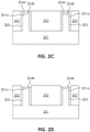
- FIG. 2A to 2E shows a shallow trench isolation (STI) recess etching operation implementing the present etching technique.
- a pad oxide 204B and a pad SiN 204A are formed over a silicon substrate 201.
- a plurality of fins 201a are formed over the silicon substrate 201 by a suitable patterning operation.
- the unremoved portions of pad oxide 204B and the pad SiN 204A are remained on the each of the fins 201a after the patterning operation.
- an STI liner 203 is selectively grown on the sidewall of the fin 201a, for example, by a SiN selective deposition operation.
- FIG. 1 shallow trench isolation
- the STI oxides 202 may be formed to cover the silicon substrate 201 and fill the space between the fins 201a.
- the pad SiN 204A and a portion of the STI liner 203 may be removed by, for example,H 3 PO 4 .
- the STI oxides 202 is recessed by an etching back operation and thereby define the fin height H fin .
- the fin height H fin as well as the shape of the fin 201a are important dimensions to be controlled because those mayaffect the electrical properties of transistors, e.g., the threshold voltage (V th ) and turn-on power etc.
- the pad oxide 204B may be removed after etching back the STIoxides 202.
- HF hydrogen fluoride
- SiO 2 etching In order to etch the STI oxides 202 made by silicon dioxide, hydrogen fluoride (HF) based chemistry is used, for instance, HF/NH 3 mixture is used for SiO 2 etching.Note the aforesaid HF/NH 3 chemistry can also remove STI liner 203 (e.g., SiN) while performing STI oxides 202 etch back. Under the circumstances that the material of the fins 201a includes silicon while the material of the STI oxides 202 includes SiO 2 , the post-etch profiles of the fins 201a may be affected during the etching operation of the STI oxides 202 if the etching selectivity between SiO 2 and Si is not sufficiently high.
- STI liner 203 e.g., SiN
- the present disclosure reduces the duration of the main etchso that said duration is shorter than an incubation time of the material not intended to be etched.
- the etching selectivity between the materials to be etched and materials not intended to be etched may thus be increasedsignificantly.
- the incubation time of a material referred in the present disclosure means the time required before observable etching result occurs to that particular material. Alternatively stated, no observable etching result may occur if the etching duration is shorter than the corresponding incubation time.
- four stages may occur during the incubation time: (a) gas phase diffusion; (b) adsorption (physisorption); (c) surface diffusion; and (d) surface reaction (chemisorption).
- Physisorped reactants are moving around the surface when they are attached by Van der Waals force, which is weak and easily desorbed, and then some of them are trapped by dipole moment force. If they find the dangling bond before they desorbed, the chemisorption is started then.
- the byproducts increased the probability to catch the reactants due to larger surface area then the reaction continues.
- the gaseous HF and NH 3 may be applied to the etching chamber. Subsequently, the gaseous HF and NH 3 may physicallyadsorb on the surface of SiO 2 .
- the adsorbedgaseous HF and NH 3 may be bounded on the surface of SiO 2 and may be mobile only in two dimensions prior to forming the interface byproduct (NH 4 ) 2 SiF 6 as follow: 6HF + 2NH 3 + SiO 2 ⁇ (NH 4 ) 2 SiF 6 + 2H 2 O That is,no observable etching result may occur to SiO 2 under HF/NH 3 chemistry until (NH 4 ) 2 SiF 6 and water are formed, and the time spend during the step (a) to step (d) may be referred as the incubation time of SiO 2 to the corresponding etching chemistry HF/NH 3 .
- FIG. 3 illustrates adiagram showingetching amountwith respect to etching duration for different material species according to some embodiments of the present disclosure. Note all the material species demonstrated in FIG. 3 are under same etching chemistry, for example, under a first etching chemistry referred herein.
- a first material M1 has a first incubation time T1 and a second material M2 has a second incubation time T2 , while the first incubation time T1 is shorter than the second incubation time T 2.
- a thirdmaterial M3, a fourth material M4, and a fifth material M5 may further be included and each of them has a third incubation time T3 , a fourth incubation time T4, and a fifth incubation time T5 ,respectively.
- the incubation times T1, T2, T3, T4, T5 of the materials M1, M2, M3, M4, M5 are all different.Note the number of the materials to a specific etching chemistry may not limit as the example shown in FIG. 3 , such figure is used to illustrate that different materials may have different incubation times, and the present disclosure utilize this feature to establish theFACS techniquefor acquiring extreme high and reversible etching selectivity.
- etching gases such as NF 3 , CF 4 , SF 6 , H 2 ,SiCl 4 , BCl 3 , or Cl 2 can be used.
- the etching gases such as CF 4 , CF 2 H 2 , CF 3 H, CFH 3 ,O 2 or CO 2 can be used.
- the material species M1 in FIG. 3 can be SiO 2 with a first incubation time T1, and any of the material species M2, M3, M4, or M5 in FIG. 3 can be Si with respective incubation times T2, T3, T4, or T5.
- T1 first incubation time
- any of the material species M2, M3, M4, or M5 in FIG. 3 can be Si with respective incubation times T2, T3, T4, or T5.
- the duration of main etch operation is within a range of from T1 to any one of T2, T3, T4, or T5
- SiO 2 (the material species M1) may demonstrate observable etching result while the Si (the material species M2, M3, M4, or M5 ) does not show any observable etching result.
- Si may serve as an etch stop layer for SiO 2 and demonstrates high etching selectivity.
- material species M1 in FIG. 3 can be SiN with an incubation time T1 of about 1.0 second, and material species M2 in FIG. 3 can be SiCN with an incubation time T2 of about 1.5 seconds.
- SiN(thematerial species M1) may demonstrate observable etching result while the SiCN (the material species M2) does not show any observable etching result.
- SiCN may serve as an etch stop layer for SiN and demonstrates high etching selectivity.
- material species M3 , M4, M5 with greater incubation time than that of SiN (the material species M1) can all serve as the etch stop layer under the aforesaid etching condition with even greater etching selectivity.
- material species M3 in FIG. 3 can be SiOCN with an incubation time T3 of about 2.0 seconds
- material species M4 in FIG. 3 can be Si with an incubation time T4 of about 2.5 seconds
- material species M5 in FIG. 3 can be SiO 2 with an incubation time T5 greater than 3 seconds.
- both SiN and SiCN may be etched without consuming SiOCN or affecting the profile of SiOCN if the duration of main etch operation is less than about 2.0 seconds (i.e., covering the time span A and time span B ) .
- time spans A, B, and C as shown in FIG.
- SiN, SiCN, and SiOCN may be etched while both the Si and the SiO 2 can serveas an etch stop material.
- the present disclosure performs incubation timesengineering by controlling the duration of main etch operation so as to enhance the etching selectivity.
- the duration of main etch is greater than 3 seconds.
- the etching selectivity between SiN and SiOCN or between SiN and SiCN are generally less than about 2:1.
- the duration of main etch is controlled to be between 1.0 second to 1.5 seconds,and the etching selectivity between SiN and SiCN is higher than about 40:1 to about 50:1, similarly, the etching selectivity between SiN and SiOCN is higher than about 100:1.
- FIGs. 4A to 4D illustrate the embodiment that may use the time span A shown in FIG. 3 for etching SiN while SiCN and SiOCN serve as etch stop materials.
- a semiconductor structure may include a plurality of source/drain regions 801 in the silicon substrate 80.
- a silicide 802 such as TiSi is disposed over some of the source/drain regions 801.
- a metal layer 803 made by W, Co or Ru is disposed over the silicide 802.
- the metal layer 803 is laterally surrounded by a bottom contact etch stop layer (BCESL) 804 made by higher temperature PEALD-grown SiN, a disposablelayer 805 made by SiOCN or SiO 2 , and a spacer 806 made by SiOCN.
- BCESL bottom contact etch stop layer
- a plurality of metal gate structures 807 which include high-k material and metal gatestack are disposed adjacent to the spacers 806.
- each of the metal gate structures 807 having a dielectric layer 808 therebelow and a contact layer 809 thereon.
- a top of the disposablelayer 805, a top of the spacer 806 and the contact layer 809 are covered by a self-align contact (SAC) 810 composed of, for example, lower temperature PEALD-grown SiN.
- SAC self-align contact
- some of thesource/drain regions 801 are covered by a plurality of cut metal gate structure 811 made by dielectric material.
- the SAC 810 may be etched back to a thin layer over the contact layer 809.
- the FACS technique as aforementioned, for example, by controlling the duration of main etch operation to be greater than the incubation time of the material of the SAC 810 (i.e., SiN) and shorter than the incubation times of the materials nearby such as the disposablelayer 805 (i.e., SiOCN or SiO 2 ), the material of the spacers 806 (i.e., SiOCN), and the metal layer 803 (i.e., W, Co or Ru), these materials nearby may thus serve as etch stop layers.
- the disposablelayer 805 i.e., SiOCN
- the spacers 806 i.e., SiOCN
- the metal layer 803 i.e., W, Co or Ru
- the etching selectivitybetween the SAC 810 and the spacer 806 is higher than about 20:1. In some embodiments, the etching selectivitybetween the SAC 810 and the metal layer 803 is higher than about 20:1. In some embodiments, the etching selectivitybetween the SAC 810 (i.e., lower temperature PEALD-grown SiN) and the BCESL 804 (higher temperature PEALD-grown SiN) is higher than about 10:1.
- the BCESL 804 is composedof SiN, since the BCESL 804 may be formed by plasma-enhanced atomic layer deposition (PEALD) with a deposition temperaturehigher than that forming the SAC 810, the incubation time of the BCESL 804 to the etching chemistry is greater than that of the SAC 810 tothe same etching chemistry.
- the SAC 810 is formed by PEALD with a temperature in a range of from about 400 Celsius degrees to about 500 Celsius degrees, while the BCESL 804 is formed by PEALD with a temperature higher than about 500 Celsius degrees, for example, of about 550 Celsius degrees.
- a recess 812 formed by the etched back of the SAC 810 may have a depth in a range of from about 8 nm to about 10 nm, for example, of about 9 nm.
- the disposablelayer 805 may be further removed in a disposable layer removal operation, and a plurality of air gaps 814 may be formed between the BCESL 804 and the spacers 806.
- a flowable STI layer 813 is spun on to seal the air gaps 814 and providing an extreme low-k layer (i.e., the air gap 814 ) in the structure.
- the incubation times of the materials species M1, M2, M3 previously shown in FIG. 3 may be changed by replacing the first etching chemistry with a second etching chemistry. That is, the order of the incubation times of the materials species M1, M2, M3 may be changed by altering the etching chemistry.
- the second etching chemistry may generate nitrogenradicals, hydrogen radicals, andoxygenradicals, and etching gases such as N 2 , or NH 3 , H 2 , O 2 or CO 2 can be used.
- the order of the incubation times for the material species M1, the materialspecies M2, and the material species M3 is changed by using the second etching chemistry.
- the materialspecies M2 can be SiCN,and the material species M3 can beSiOCN.
- SiCN has ashorter incubation times T6 than the incubation time T7 of SiOCN.
- incubation times T6 and T7 are about 1.0 second and 1.5 seconds respectively,while the materialspecies M1, SiN,has a longer incubation time T8 of about 2.0 seconds.
- SiCN is etched while SiOCN and SiN can serve as etch stop materials.
- both SiCN and SiOCN are etched while SiN can serve as an etch stop material.
- each of the etching cycles/periods in CDE is no less than about 3 seconds by taking uniform chemisorption and plasma stability into consideration.
- the duration of the main etch is to be greater than about 3 seconds
- only the fifth material M5 i.e., SiO 2
- the fifth material M5 can be used as an etch stop material with high selectivity because such long duration of the main etch exceeds the incubation time of most of the material species shown in FIG. 3 .
- each of the materials has a specific incubation time to a specific etching chemistry
- the present disclosure may utilize the orders of the incubation times to enable high etch selectivity and reversible etching technique. That is, the present disclosure may broaden the applicabilityof the etching apparatus under the fact that a single etching apparatus may thus be used to provide multiple etching modes.
- etching chemistries when a variety of etching chemistries can be integrated to one etching apparatus,the wafers under process are no longer required to transfer from one etching chamber providing one or few etching chemistries to another etching chamber providing other one or other few etching chemistries when the material intended to be etched is changed along the manufacturing operations.
- a singleetching apparatus can only be used to implement one or few etching operations (e.g., the first material is etched and the second material serves as etch stop) and the wafers have to be moved to another etching apparatus to implement another one or few etching operations (e.g., the second material is etched and the third material serves as etch stop).
- each of the materials intended to be etched may be etched by different etching chemistries with different incubation times, and therefore it is feasible to perform a reversible etching selectivity operations without transferring the wafer from one etching apparatus to another etching apparatus.
- material species M1 e.g., SiN
- material species M2 e.g., SiCN
- material species M3 e.g., SiOCN
- the etching chamber performing the etching of the material species M1 can change to the second etching chemistry of FIG. 5 , when performing the main etch with a duration falls within the time span D or E, material species M2 (e.g., SiCN) and material species M3 (e.g., SiOCN) are etched while species M1 (e.g., SiN) reversibly serve as etch stop with high etching selectivity.
- material species M2 e.g., SiCN
- material species M3 e.g., SiOCN
- the manufacturingtechnique may include operation 301 :receiving a semiconductor structure having a first material and a second material; an operation 302: pretreating the semiconductor structure; and an operation 303: subsequent to pretreating the semiconductor structure, performing a first main etch to the semiconductor structure for a duration undera first etchingchemistry.
- the first material and the second material having different incubation timesunderthe first etching chemistry.
- the pretreatment to the semiconductor structure prior to the first main etch allows the shortening of the duration of the main etch so that the duration of the main etch can be shorter than one of the incubation times that provides high etching selectivity to the first material and the second material.
- the FACS technique disclosed in the present disclosure may include a plurality of first main etches 401 in a cyclic etching fashion.
- the etching chemistry Prior to each of the first main etches 401 , the etching chemistry may be applied into the etching chamber and therefore the pressure is increased to reach a suitableetching pressure P E .
- the etching pressure P E of performing the first main etch 401 is greater than about 10 torr.
- a higher etching pressure may enhance etching selectivity,for example, the etching selectivity of SiO 2 /SiN may be enhanced from about 20 to about 140 when the etching pressure is increased from lower than 3 torr to greater than 10 torr.
- the increasing of the etching pressure may increase the flow rate of the etching gas, and the step (a) in the incubation time (i.e., gas phase diffusion) as aforementioned may be accelerated. Moreover, a higher flow rate of the etching gas may increase the etch rate by accelerating the absorption/desorption process of the reactants.
- the etching pressure P E or the flow rate of the etching gas By increasing the etching pressure P E or the flow rate of the etching gas,the duration of the main etch implemented in the embodiments of present disclosure can be reduced.
- the etching pressure P E applied may also lead to reduction of the incubation time of the corresponding material species.
- the manufacturingtechnique may further include a pumping period 403 between first main etches 401 in sequential order.
- the pumping period 403 the etching chemistry may be pumped out from the etching chamber and therefore the pressure in the etching chamber may be decreased to about zero.
- the manufacturingtechnique may further include a plurality of pretreatments 404 to the etching surface prior to each of the first main etches 401 .
- the pretreatments 404 applied to the etching surface may include one of a catalyzing operation, a surface cleaning operation, or a passivation operation.
- catalyst for example, hydrogen radicals
- surface cleaning to the etching surface during pretreatment 404 can effectively remove the unreacted chemical or undesorbed products from the etching surface prior to the subsequent main etch.
- the etching byproducts such as fluorine or chlorine absorbed on the surface of the etching surface can be removedduring the pretreatment 404 .
- the pretreatment 404 may include applying gas sources such as HF, NH 3 , F 2 , NF 3 , H 2 O, H 2 , CH 4 , Cl 2 , SiCl 4 , FCl 3 , CH 3 F, O 2 , BCl 3 , N 2 , and the like, to the etching surface, depending on the etching chemistry and the material speciesof the etching surface.
- gas sources such as HF, NH 3 , F 2 , NF 3 , H 2 O, H 2 , CH 4 , Cl 2 , SiCl 4 , FCl 3 , CH 3 F, O 2 , BCl 3 , N 2 , and the like.
- passivation gas for example, polymeric gas
- the increase of etching pressure P E and the implementation of pretreatments 404 can effectively reduce the duration of main etch, thereby allowing incubation time engineering that leads to high and reversible selectivity etching result.
- the duration of the main etch in the present disclosure can be controlled within the time span A, hence only predetermined materials in the semiconductor structure may be etched without consuming or affecting the profiles of other materials having longer incubation times to the first etching chemistry.
- each of the first durations T51 i.e., the duration of the first main etch
- each of the first durations T51 isin a range of from about 1 second to about 2.5 seconds.
- the corresponding pumping period may be within a range of from about 5 seconds to about 180 seconds.
- the pumping duration T51' can be reduced, for example, from about 5 seconds to about 60 seconds. Shorter pumping duration T51' and more frequent pumping period 403 can lead to the advantage of etching profile decoration, as will be discussed in FIG. 9A to FIG. 9B and FIG. 10A to FIG. 10C of the present disclosure.
- At least one second main etch 402 to the etching surface may be performed for a second duration T52 (i.e., the duration of the second main etch 402 ) subsequent to performing the first main etch 401 .
- the second duration T52 is greater than the first incubation time (e.g., time span A in FIG. 3 ) but shorter than the second incubation time (e.g., time span B in FIG. 3 ) .
- each of the second durations T52 are less than about 3.0 seconds.
- each of the second durations T52 are in a range of from about 1 second to about 2.5 seconds.
- the second duration T52 is substantially identical to the first duration T51 .
- the second main etch 402 may be substantially identical to the first main etch 401 and thus the first main etches 401 are substantially implemented repeatedly.
- the first main etch 401 and the second main etch 402 may fall within different time spans under the same etching chemistry, such as previously mentioned in FIG. 3 or FIG. 5 . Therefore, the materials intended to be etched during the first main etch 401 and the second main etch 402 may be different, and both the first main etch 401 and the second main etch 402 demonstrate high etching selectivity.
- the etching chemistry is altered from the first etch chemistry to the second etch chemistry and thus the reversible etching techniquethat broaden the applicabilityof the etching apparatus as previously described may be performed.
- the second material serves as an etch stop material to the first etching chemistry during the first main etch 401 and may be changed to be the material intended to be etched during the second main etch 402 .
- the first duration T51 and the second duration T52 can be independently determined because the first main etch 401 and the second main etch 402 are implemented under different etching chemistries and the incubation time corresponding to respective material species may be different as the previously shown in FIG. 3 and FIG. 5 .
- the FACS technique may be used for profile decoration, for example, de-smiling,reducesurfaceroughness, and greater etched surface uniformity.
- the FACStechnique may include an operation 801 :receiving a semiconductor structure having a first material;an operation 802: performing afirst main etch to the semiconductor structure for afirst durationunderthe first etching chemistry; and operation 803: performing a pumping operation prior to performing the first main etch for a pumping duration, wherein the first duration is in a range of from about 1 second to about 2.5 seconds.
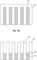
- FIG. 9A to FIG. 9B shows an etching operation to form closely arranged nitride hard mask601by removing surrounding oxide material 602 .
- the reduced duration of main etch allows more frequent pumping periods and greater number of cyclic etching per unit time, therefore, a better surface profile of the nitride hard mask 601 can be obtained.
- a plurality ofnitride hard mask 601 are formed and the gaps therebetween are subsequently filled with oxide material 602.
- a top surface of the oxide material 601 may be higher than a top surface of the plurality of nitride hard mask 602 .
- the profiles of the nitride hard mask 601 in the regions 603 that close to the tops of the nitride hard mask 601 may be maintained as much as possible.
- the planar profiles of the nitride hard mask 601 in the regions 603 and the planar profile of the post-etch oxide material 602 in the region 604 may be substantially preservedafter etching under the FACS technique.
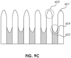
- rounded post-etch profile of the nitride hard mask 601' in the region 603' may be observed.
- prominent smiling profile of the post-etch surface of the oxide material 602' in the region 604' can be observed when utilizing conventional CDE approach.
- FIG. 10A to FIG. 10C show etching operations to recess SiGe layer 605 from the SiGe/Si stack.
- the reduced duration of main etch allows more frequent pumping periods and greater number of cyclic etching per unit time, therefore, a better surface profile of the SiGe layer can be obtained.
- the stacked Si layers 604 and SiGe layers 605 are formed.
- Si nano-sheets 604' is preliminary released by a plurality of SiGe recesses 606.
- HF/F 2 may be used as the etching chemistry and a portion of the SiGe layers 605is etched under the FACStechniqueto form the partially etchedSiGe 605' and the SiGe recesses 606.
- the SiGe recesses 606 may be covered with inner spacers 607 subsequently.
- etching selectivity between SiGe layers 605 and Si layers 604 is high and the etch frontof each of the SiGe recesses 606 may preserve a substantially vertical planar profile than the structure obtained by conventional CDE approach.
- the etch front 606A of the SiGe recess 606 formed under the FACS technique may have a lower curvature (larger radius of curvature), while the etch front 606B (dotted lines) of the SiGe recess 606 formed by conventional CDE approach may have a greatercurvature (smaller radius of curvature).
- the phenomenon regarding the decelerated etching around the corners of the recesses may be alleviated by the FACS technique. Therefore,the electrical and otherperformance of the semiconductor structures may be ensured.
- the inner spacers 607 may be deposited on the profiles of the SiGe recesses 606, and further be trimmed by FACStechnique subsequently.
- the substantially vertical sidewall profiles of the Si nano-sheets 604' may be maintained as much as possible under the FACS technique.
- the smilingprofile(i.e., the extent of recess is greater at the center and smaller at the corner) at the etch front may be alleviated.
- the byproducts of etching may cluster at the kinks or the steps of the semiconductor structure, for example, as the embodiments shown in FIG. 9B and FIG. 10B
- the byproducts such as (NH 4 ) 2 SiF 6 formed from SiO 2 etching and Ge residues formed from SiGe etching may be adsorbed on the surfaces in proximity to the corners of the STI recesses and the SiGe recesses respectively.
- the etching chemistry may not access the material intended to be etched and thus the etching rate at the corner is lower than that around the centers of the recesses.
- the lowering of the etching rate is highly related to the length of etching duration, because the longer of the etching duration is, the more byproducts are clustered at the kinks or the steps of the etching surface. Accordingly, by using the FACStechnique, the duration of main etch cycleis limited to be shorter than the incubation times of predetermined materials to the etching chemistry. Therefore, the byproducts may be removed shortly and repeatedlythrough the pumping periods 403 and the pretreatment 404 shown in FIG. 7A and FIG. 7B . That is, the FACStechnique maycyclically clean the byproducts at the kinks or the steps of the semiconductor structure and thus alleviate the forming of the smiling curves.
- more pumping periods 403 provided by the FACS technique also may benefit to reducing roughness of the etch front 606B of the SiGe layers 605.
- it is harder to remove germanium components from the SiGe layer 605 under the etching chemistry.
- Ge removal efficiency is poor and Ge islands may be remained at the etch front of the etched SiGe 605', thereby causingpoor surface roughness at the etch front.
- by implementing more frequent pumping periods 403 as described in FIGs. 7A and 7B Ge removal efficiency can be increased and hence the surface roughness decreased.
- FIG. 7A and 7B As illustrated in FIG.
- the roughness of the etch front 606A can be less than about 4 nm, for example, around or less than 3.5 nm. In some embodiments, the roughness of the etch front 606A may be reduced by increasing the frequency of pumping periods and the number of cyclic etching per unit time.
- FIG. 11A and FIG. 11B show etching operations to recess SiGe layer 605 from the SiGe/Si stack.
- the reduced duration of main etch allows more frequent pumping periods and greater number of cyclic etching per unit time, therefore, a better surface profile of the SiGe layer can be obtained.
- a plurality of fins 701 is covered by low-k material 702 such as SiCN or SiOCN.
- low-k material 702 such as SiCN or SiOCN.
- seams 703 can be observed by virtue of adoptingatomic layer deposition (ALD).
- the buried seams 703 can be filled by using the passivation operation during the pretreatment 404 applied in the FACStechnique shown in FIG. 7A and FIG. 7B .
- the materials used inpassivation operation of the pretreatment 404 may include polymer-forming gases including components of CH 4 or SiCl 4 so that the byproducts may fill the seams 703 as much as possible.
- the structural defects due to ALD operations may be cured by the FACS technique by preventinga greater etching rate nearby the seams 703.
- a method or a technique for semiconductor manufacturing includes Fast Assess Cyclic Switching (FACS) technique which interrupts the etching operation prior to the end of the incubation times of etch stop materials, and thus the etching is terminated prior to those etch stop materialsstart having observable etching result.
- FACS Fast Assess Cyclic Switching
- CDE chemical dry etch
- FACS technique enables extreme high and reversible selectivity through incubation time engineering and advanced profile decoration skills including de-smiling, depth variation and surface roughness control, and therefore the yield and the performance of the semiconductor structure may be improved.
- atechnique for semiconductor manufacturing includes the operations as follows.
- a semiconductor structure having a first material and a second material is received.
- the first material has a first incubation time to a first etching chemistry.
- the second material has a second incubation time to the first etching chemistry.
- the first incubation time is shorter than the second incubation time.
- a first main etch to the semiconductor structure for a first duration by the first etching chemistry is performed. The first duration is greater than the first incubation time and shorter than the second incubation time.
- a technique for semiconductor manufacturing includes the operations as follows.
- a semiconductor structure having a first material and a second material is received.
- the first material having a first incubation time and the second material having a second incubation time greater than the first incubation timeunder a first etching chemistry.
- the semiconductor structure is pretreated.
- a first main etch is performed to the semiconductor structure for a duration under the first etchingchemistrysubsequent to pretreating the semiconductor structure.
- a technique for semiconductor manufacturing includes the operations as follows.
- a semiconductor structure having a first material is received.
- a plurality of first main etches are performed to the semiconductor structure for a plurality of first durationsunderthe first etching chemistry.
- a plurality of pumping operations are performed for a plurality ofpumping durations, each of the pumping operations being prior to each of the first main etches.Each of the first durations is in a range of from about 1 second to about 2.5 seconds.
Landscapes
- Drying Of Semiconductors (AREA)
- Physics & Mathematics (AREA)
- Engineering & Computer Science (AREA)
- Plasma & Fusion (AREA)
Abstract
A technique for semiconductor manufacturing is provided. The technique includes the operations as follows. A semiconductor structure having a first material and a second material is revived. The first material has a first incubation time to a first etching chemistry.The second material has a second incubation time to the first etching chemistry.The first incubation time is shorter than the second incubation time. A first main etch to the semiconductor structure for a first duration by the first etching chemistry is performed.The first duration is greater than the first incubation time and shorter than the second incubation time.
Description
- The present disclosure relates to a techniquefor dry etching, particularly, the technique is related tochemical dry etching (CDE)operation.
- In dry etching, plasmas or etchant gases remove the material on the substrate. The reaction that takes place can be done utilizing high kinetic energy of particle beams, chemical reaction, or a combination of both.
- Dry etching may includephysical component and chemical component. Physical component requires high kinetic energy particle or ion beams to bombard surface atoms. When the high energy particles knock out the atoms from the surface, the material turns into gaseous phase and being evacuatedafter leaving the surface. In contrast, chemical component uses a chemical reaction between etchant gases and the surfacematerial. Products of the chemical reaction may be subsequently removed from the etching chamber.
- Aspects of the present disclosure are best understood from the following detailed description when read with the accompanying figures. It is noted that, in accordance with the standard practice in the industry, various structures are not drawn to scale. In fact, the dimensions of the various structures may be arbitrarily increased or reduced for clarity of discussion.
-
FIG. 1 illustrates a flow chart ofa technique for semiconductor manufacturing,according to some embodiments of the present disclosure. -
FIG. 2A illustrates across-sectional view ofan intermediatesemiconductor structure when performing the technique for semiconductor manufacturing, according to some embodiments of the present disclosure. -
FIG. 2B illustrates across-sectional view ofan intermediatesemiconductor structure when performing the technique for semiconductor manufacturing, according to some embodiments of the present disclosure. -
FIG. 2C illustrates across-sectional view ofan intermediatesemiconductor structure when performing the technique for semiconductor manufacturing,according to some embodiments of the present disclosure. -
FIG. 2D illustrates across-sectional view ofan intermediatesemiconductor structure when performing the technique for semiconductor manufacturing,according to some embodiments of the present disclosure. -
FIG. 2E illustrates across-sectional view ofan intermediatesemiconductor structure when performing the technique for semiconductor manufacturing, according to some embodiments of the present disclosure. -
FIG. 3 illustrates adiagram showingetching amountwith respect to etching duration for different material species according to some embodiments of the present disclosure. -
FIG. 4A illustrates across-sectional view ofan intermediatesemiconductor structure when performing the technique for semiconductor manufacturing, according to some embodiments of the present disclosure. -
FIG. 4B illustrates across-sectional view ofan intermediatesemiconductor structure when performing the technique for semiconductor manufacturing, according to some embodiments of the present disclosure. -
FIG. 4C illustrates across-sectional view ofan intermediatesemiconductor structure when performing the technique for semiconductor manufacturing, according to some embodiments of the present disclosure. -
FIG. 4D illustrates across-sectional view ofan intermediatesemiconductor structure when performing the technique for semiconductor manufacturing, according to some embodiments of the present disclosure. -
FIG. 5 illustrates adiagram showingetching amountwith respect to etching duration for different material species according to some embodiments of the present disclosure. -
FIG. 6 illustrates a flow chart of a technique for semiconductor manufacturing, according to some embodiments of the present disclosure. -
FIG. 7A illustrates adiagram showing etching pressure with respect to etching duration and pumping durationaccording to some embodiments of the present disclosure. -
FIG. 7B illustrates adiagram showing etching pressure with respect to etching duration and pumping durationaccording to some embodiments of the present disclosure. -
FIG. 8 illustrates a flow chart of a technique for semiconductor manufacturing, according to some embodiments of the present disclosure. -
FIG. 9A illustrates across-sectional view ofan intermediatesemiconductor structure when performing the technique for semiconductor manufacturing,according to some embodiments of the present disclosure. -
FIG. 9B illustrates across-sectional view ofan intermediatesemiconductor structure when performing the technique for semiconductor manufacturing,according to some embodiments of the present disclosure. -
FIG. 9C illustrates across-sectional view ofan intermediatesemiconductor structure without using the technique, according to some comparative embodiments of the present disclosure. -
FIG. 10A illustrates across-sectional view ofan intermediatesemiconductor structure when performing the technique for semiconductor manufacturing,according to some embodiments of the present disclosure. -
FIG. 10B illustrates across-sectional view ofan intermediatesemiconductor structure when performing the technique for semiconductor manufacturing,according to some embodiments of the present disclosure. -
FIG. 10C illustrates across-sectional view ofan intermediatesemiconductor structure when performing the technique for semiconductor manufacturing,according to some embodiments of the present disclosure. -
FIG. 11A illustrates across-sectional view ofan intermediatesemiconductor structure when performing the technique for semiconductor manufacturing,according to some embodiments of the present disclosure. -
FIG. 11B illustrates across-sectional view ofan intermediatesemiconductor structure when performing the technique for semiconductor manufacturing,according to some embodiments of the present disclosure. - The following disclosure provides many different embodiments, or examples, for implementing different features of the provided subject matter.Specific examples of elements and arrangements are described below to simplify the present disclosure.These are, of course, merely examples and are not intended to be limiting.For example, the formation of a first feature over or on a second feature in the description that follows may include embodiments in which the first and second features are formed in direct contact, and may also include embodiments in which additional features may be formed between the first and second features, such that the first and second features may not be in direct contact.In addition, the present disclosure may repeat reference numerals and/or letters in the various examples. This repetition is for the purpose of simplicity and clarity and does not in itself dictate a relationship between the various embodiments and/or configurations discussed.
- Further, spatially relative terms, such as "beneath," "below," "lower," "above," "upper", "on" and the like, may be used herein for ease of description to describe one element or feature's relationship to another element(s) or feature(s) as illustrated in the figures. The spatially relative terms are intended to encompass different orientations of the device in use or operation in addition to the orientation depicted in the figures. The apparatus may be otherwise oriented (rotated 90 degrees or at other orientations) and the spatially relative descriptors used herein may likewise be interpreted accordingly.
- As used herein, the terms such as "first", "second" and "third" describe various elements, components, regions, layers and/or sections, these elements, components, regions, layers and/or sections should not be limited by these terms. These terms may be only used to distinguish one element, component, region, layer or section from another. The terms such as "first", "second", and "third" when used herein do not imply a sequence or order unless clearly indicated by the context.
- When critical dimensions of semiconductor structures are decreased, more and more applications require selective, isotropic, and nearly damage-free etching. As architecture changed from FinFET to nano-sheet,for example, two additional operationsoccur for lateral silicon germanium (SiGe) etching with selectivity to silicon (Si). The high energy ion bombardment from plasma-based processes may suffer several problems including: (1) low etch selectivity; (2) limited lateral etching capability; and (3) defects degrading the quality of the structure. Even though some wet etching techniques could alleviate these concerns, limited within-wafer uniformity tuning, profile decoration and narrow gap etching capability still constrained their applications.
- An alternative strategy is chemical dry etch (CDE) by either gaseous or radical species. The radical fluxes can be produced by a remote plasma source (RPS), in which flow distance or the use of grids largely eliminates ion fluxes and delivers neutral radicals into the process chamber where the wafer is placed. Generally, each of the etching cycles/periods in CDE is no less than 3 seconds by taking uniform chemisorption and plasma stability into consideration.
- Generally speaking, four categories of parameters or tuning knobs can be implemented for suitable etching result, namely, chemistry (e.g., radical or gas species, power of remote plasma source), temperature (e.g., lid/wall temperature for gaseous phase reaction, wafer temperature for gaseous/solid surface reaction), pressure (e.g., adsorption/desorption), and cyclic operation with each cycle no less than 3 seconds. The aforesaid four tuning knobs, however, cannot meet the demand of high and reversible etching selectivity, and cannot produce fine feature profile decoration due to unavoidable non-uniform by-product accumulation and different etching incubation time for different material species.
- Accordingly, the present disclosure provides a new technique for manufacturing a semiconductor structure by using fast assess cyclic switching (FACS) technique. FACS may be performed based on a CDEoperation. In some embodiments, FACS may shorten the minimum acceptable etchingduration per cycle/period downto 1 second. Such novel technique enables high and reversible etching selectivity through incubation time engineering. In addition,FACS can make significant progress indeveloping the profile decoration such as de-smiling, depth variation and surface roughness.
-
FIG. 1 illustrates a flow chart of manufacturinga semiconductor structureaccording to some embodiments of the present disclosure. In some embodiments, the manufacturing technique includes an operation 101: receiving a semiconductor structure having a first material and a second material; and an operation 102: performing a first main etch to the semiconductor structure for a first duration by afirst etching chemistry, wherein the first duration is greater than a first incubation time of the first material and shorter than a second incubation time of the second material under the first etching chemistry. For example, the manufacturingtechniqueis implemented under the circumstances that the first material having a first incubation time to the first etching chemistry, the second material having a second incubation time to the first etching chemistry, and the first incubation time is shorter than the second incubation time. The first duration that the first main etch lasts is greater than the first incubation time and shorter than the second incubation time, so that a high etching selectivity between the first material and the second material can be achieved. - In some embodiments, the first material includes silicon or silicon compounds such as silicon nitride (SiN), silicon carbon nitride (SiCN), silicon dioxide (SiO2),silicon oxycarbonitride (SiOCN), silicon carbide (SiC), or SiGe. In some embodiments, the first material includes other oxides, nitrides, or conductive materials that used in forming the semiconductor structures. In some embodiments, the second material includes silicon or silicon compounds such as SiN, SiCN, SiO2, SiOCN, SiC, or SiGe. In some embodiments, the second material includes other oxides, nitrides, or conductive materials that used in forming the semiconductor structures. In some embodiments, the first material is different from the second material.
- Under a predetermined etching chemistry, different materials (e.g., first material serving as a material to be etched and second material serving as an etch stop) do not necessary show sufficient etching selectivitywhen the duration of main etch is greater than both the first incubation time of the first material and the second incubation time of the second material. Present disclosure provides an etching technique for semiconductor manufacturing to shorten the duration of the main etch so that the duration of the main etch can be shorter than the second incubation time and longer than the first incubation time. This incubation time engineering can effectively increase the etching selectivity between the first material and the second material.
FIGs. 2A to 2E shows a shallow trench isolation (STI) recess etching operation implementing the present etching technique.InFIG. 2A , apad oxide 204B and apad SiN 204A are formed over asilicon substrate 201. Next, a plurality offins 201a are formed over thesilicon substrate 201 by a suitable patterning operation. The unremoved portions ofpad oxide 204B and thepad SiN 204A are remained on the each of thefins 201a after the patterning operation. InFIG. 2B , anSTI liner 203 is selectively grown on the sidewall of thefin 201a, for example, by a SiN selective deposition operation. InFIG. 2C , theSTI oxides 202 may be formed to cover thesilicon substrate 201 and fill the space between the fins 201a.InFIG. 2D , thepad SiN 204A and a portion of theSTI liner 203 may be removed by, for example,H3PO4. InFIG. 2E ,theSTI oxides 202 is recessed by an etching back operation and thereby define the fin height Hfin. The fin height Hfin as well as the shape of thefin 201a are important dimensions to be controlled because those mayaffect the electrical properties of transistors, e.g., the threshold voltage (Vth) and turn-on power etc. In some embodiments, thepad oxide 204B may be removed after etching back theSTIoxides 202. - In order to etch the
STI oxides 202 made by silicon dioxide, hydrogen fluoride (HF) based chemistryis used, for instance, HF/NH3 mixture is used for SiO2 etching.Note the aforesaid HF/NH3 chemistry can also remove STI liner 203 (e.g., SiN) while performingSTI oxides 202 etch back. Under the circumstances that the material of thefins 201a includes silicon while the material of theSTI oxides 202 includes SiO2, the post-etch profiles of thefins 201a may be affected during the etching operation of theSTI oxides 202 if the etching selectivity between SiO2 and Si is not sufficiently high. Accordingly, the present disclosure reduces the duration of the main etchso that said duration is shorter than an incubation time of the material not intended to be etched. The etching selectivity between the materials to be etched and materials not intended to be etched may thus be increasedsignificantly. - The incubation time of a material referred in the present disclosure means the time required before observable etching result occurs to that particular material. Alternatively stated, no observable etching result may occur if the etching duration is shorter than the corresponding incubation time. Generally, four stages may occur during the incubation time: (a) gas phase diffusion; (b) adsorption (physisorption); (c) surface diffusion; and (d) surface reaction (chemisorption). Physisorped reactants are moving around the surface when they are attached by Van der Waals force, which is weak and easily desorbed, and then some of them are trapped by dipole moment force. If they find the dangling bond before they desorbed, the chemisorption is started then. Once chemisorption occurs and forms the byproducts such as ammonium fluorosilicate, the byproducts increased the probability to catch the reactants due to larger surface area then the reaction continues. For instance, by using HF/NH3 mixture in SiO2 etching, the gaseous HF and NH3 may be applied to the etching chamber. Subsequently, the gaseous HF and NH3 may physicallyadsorb on the surface of SiO2. Next, the adsorbedgaseous HF and NH3 may be bounded on the surface of SiO2 and may be mobile only in two dimensions prior to forming the interface byproduct (NH4)2SiF6 as follow:
6HF + 2NH3 + SiO2→ (NH4)2SiF6 + 2H2O
That is,no observable etching result may occur to SiO2 under HF/NH3 chemistry until (NH4)2SiF6 and water are formed, and the time spend during the step (a) to step (d) may be referred as the incubation time of SiO2 to the corresponding etching chemistry HF/NH3. -
FIG. 3 illustrates adiagram showingetching amountwith respect to etching duration for different material species according to some embodiments of the present disclosure. Note all the material species demonstrated inFIG. 3 are under same etching chemistry, for example, under a first etching chemistry referred herein. InFIG. 3 ,a first materialM1 has a first incubation timeT1 and a second materialM2 has a second incubation timeT2, while the first incubation timeT1 is shorter than the second incubation timeT2. Likewise, a thirdmaterial M3, a fourth material M4, and a fifth material M5 may further be included and each of them has a third incubation timeT3, a fourth incubation time T4, and a fifth incubation time T5,respectively. As the example shown inFIG. 3 , the incubation times T1, T2, T3, T4, T5 of the materials M1, M2, M3, M4, M5 are all different.Note the number of the materials to a specific etching chemistry may not limit as the example shown inFIG. 3 , such figure is used to illustrate that different materials may have different incubation times, and the present disclosure utilize this feature to establish theFACS techniquefor acquiring extreme high and reversible etching selectivity. - Different etching chemistries lead to different combinations of the etching amount, incubation times, and material species, as illustrated in
FIG. 3 . For example, under the etching chemistry generatingfluorineradicals (F-), hydrogenradicals (H+), and chlorine radicals (Cl-), etching gases such as NF3, CF4, SF6, H2,SiCl4, BCl3, or Cl2 can be used. In other embodiments, under the etching chemistry generating fluorocarbonradicals or oxygenradicals, the etching gases such as CF4, CF2H2, CF3H, CFH3,O2 or CO2 can be used. By implementing a suitable etching chemistry and controlling the duration of main etch to be between two of the incubation times of the corresponding material species, theFACS technique described herein can be achieved. - Referring to
FIG. 2A to FIG. 2E andFIG. 3 , under the chemistry of HF/NH3, the material species M1 inFIG. 3 can be SiO2 with a first incubation time T1, and any of the material species M2, M3, M4, or M5 inFIG. 3 can be Si with respective incubation times T2, T3, T4, or T5. Once the duration of main etch operation is within a range of from T1 to any one of T2, T3, T4, or T5, SiO2 (the material species M1) may demonstrate observable etching result while the Si (the material species M2, M3, M4, or M5) does not show any observable etching result. Hence, Si may serve as an etch stop layer for SiO2 and demonstrates high etching selectivity. - In some embodiments, under the etching chemistry includingetching gases NF3, CF4, SF6, H2, SiCl4, BCl3, or Cl2, material species M1 in
FIG. 3 can be SiN with an incubation time T1 of about 1.0 second, and material species M2 inFIG. 3 can be SiCN with an incubation time T2 of about 1.5 seconds. As an example, once the duration ofmain etchoperation is withina range of from T1 (e.g., about 1.0 second) toT2 (e.g., about 1.5 seconds) or within the time span A, SiN(thematerial species M1) may demonstrate observable etching result while the SiCN (the material species M2) does not show any observable etching result. Hence, once the duration of the main etch operationis controlled to be from 1.0 second to about 1.5 seconds, SiCN may serve as an etch stop layer for SiN and demonstrates high etching selectivity. Similarly, material speciesM3, M4, M5 with greater incubation time than that of SiN (the material species M1) can all serve as the etch stop layer under the aforesaid etching condition with even greater etching selectivity. - Further in such example, material species M3 in
FIG. 3 can be SiOCN with an incubation time T3 of about 2.0 seconds, material species M4 inFIG. 3 can be Si with an incubation time T4 of about 2.5 seconds, and material species M5 inFIG. 3 can be SiO2 with an incubation time T5 greater than 3 seconds. Similarly, both SiN and SiCN may be etched without consuming SiOCN or affecting the profile of SiOCN if the duration of main etch operation is less than about 2.0 seconds (i.e., covering the time span A and time span B). Similarly, during the time spans A, B, and C as shown inFIG. 3 ,SiN, SiCN, and SiOCN may be etched while both the Si and the SiO2 can serveas an etch stop material.In other words, the present disclosure performs incubation timesengineering by controlling the duration of main etch operation so as to enhance the etching selectivity. In some conventional approaches where FACS technique is not implemented, the duration of main etch is greater than 3 seconds. The etching selectivity between SiN and SiOCN or between SiN and SiCN are generally less than about 2:1. However, when implementing the FACS technique,the duration of main etch is controlled to be between 1.0 second to 1.5 seconds,and the etching selectivity between SiN and SiCN is higher than about 40:1 to about 50:1, similarly, the etching selectivity between SiN and SiOCN is higher than about 100:1. -
FIGs. 4A to 4D illustrate the embodiment that may use the time span A shown inFIG. 3 for etching SiN while SiCN and SiOCN serve as etch stop materials. As shown inFIG. 4A , a semiconductor structure may include a plurality of source/drain regions 801 in thesilicon substrate 80. Asilicide 802 such as TiSi is disposed over some of the source/drain regions 801. A metal layer803 made by W, Co or Ru is disposed over thesilicide 802. The metal layer803 is laterally surrounded by a bottom contact etch stop layer (BCESL)804 made by higher temperature PEALD-grown SiN, adisposablelayer 805 made by SiOCN or SiO2, and aspacer 806 made by SiOCN. Furthermore, a plurality ofmetal gate structures 807 which include high-k material and metal gatestack are disposed adjacent to thespacers 806. In some embodiments, each of the metal gate structures 807having adielectric layer 808 therebelow and acontact layer 809 thereon. In some embodiments, a top of thedisposablelayer 805, a top of thespacer 806 and thecontact layer 809 are covered by a self-align contact (SAC) 810composed of, for example, lower temperature PEALD-grown SiN. In some embodiments, some of thesource/drain regions 801 are covered by a plurality of cut metal gate structure811 made by dielectric material. - In such embodiments, as shown in
FIG. 4B , theSAC 810 may be etched back to a thin layer over thecontact layer 809. By using the FACS technique as aforementioned, for example, by controlling the duration of main etch operation to be greater than the incubation time of the material of the SAC 810 (i.e., SiN) and shorter than the incubation times of the materials nearby such as the disposablelayer 805 (i.e., SiOCN or SiO2), the material of the spacers 806 (i.e., SiOCN), and the metal layer803 (i.e., W, Co or Ru), these materials nearby may thus serve as etch stop layers. In some embodiments, the etching selectivitybetween theSAC 810 and thespacer 806 is higher than about 20:1. In some embodiments, the etching selectivitybetween theSAC 810 and the metal layer803 is higher than about 20:1. In some embodiments, the etching selectivitybetween the SAC 810 (i.e., lower temperature PEALD-grown SiN) and the BCESL804 (higher temperature PEALD-grown SiN) is higher than about 10:1. - Although the BCESL804 is composedof SiN, since the BCESL804 may be formed by plasma-enhanced atomic layer deposition (PEALD) with a deposition temperaturehigher than that forming the
SAC 810, the incubation time of the BCESL804 to the etching chemistry is greater than that of the SAC 810tothe same etching chemistry. In some embodiments, theSAC 810 is formed by PEALD with a temperature in a range of from about 400 Celsius degrees to about 500 Celsius degrees, while the BCESL804 is formed by PEALD with a temperature higher than about 500 Celsius degrees, for example, of about 550 Celsius degrees. As shown inFIG. 4B , a recess812 formed by the etched back of theSAC 810 may have a depth in a range of from about 8 nm to about 10 nm, for example, of about 9 nm. - As shown in
FIG. 4C , in some embodiments, thedisposablelayer 805 may be further removed in a disposable layer removal operation, and a plurality of air gaps814 may be formed between the BCESL804 and thespacers 806. As shown inFIG. 4D , in some embodiments, aflowable STI layer 813 is spun on to seal theair gaps 814 and providing an extreme low-k layer (i.e., the air gap 814) in the structure. - As shown in
FIG. 5 , the incubation times of the materials species M1, M2, M3previously shown inFIG. 3 may be changed by replacing the first etching chemistry with a second etching chemistry. That is, the order of the incubation times of the materials species M1, M2, M3may be changed by altering the etching chemistry.In some embodiments, the second etching chemistry may generate nitrogenradicals, hydrogen radicals, andoxygenradicals, and etching gases such as N2, or NH3, H2, O2 or CO2 can be used. - As shown in
FIG. 5 , the order of the incubation times for the material species M1, the materialspecies M2, and the material species M3is changed by using the second etching chemistry.For instance, as previously described inFIG. 3 , the materialspeciesM2 can be SiCN,and the material species M3 can beSiOCN. Under the second etching chemistry, SiCNhas ashorter incubation times T6 than the incubation time T7of SiOCN. For example,incubation timesT6 and T7 are about 1.0 second and 1.5 seconds respectively,while the materialspecies M1, SiN,has a longer incubation time T8 of about 2.0 seconds. Accordingly,when the duration of the main etch falls within the time spanD, SiCN is etched while SiOCN and SiN can serve as etch stop materials. Likewise, when the duration of the main etch falls within the time span E, both SiCN and SiOCN are etched while SiN can serve as an etch stop material. - As previously discussed, currently each of the etching cycles/periods in CDE is no less than about 3 seconds by taking uniform chemisorption and plasma stability into consideration. Referring to
FIG. 3 , under the first chemistry scenario, when the duration of the main etch is to be greater than about 3 seconds, only the fifth material M5 (i.e., SiO2) can be used as an etch stop material with high selectivity becausesuch long duration of the main etch exceeds the incubation time of most of the material species shown inFIG. 3 . Likewise, referring toFIG. 5 , under the second chemistry scenario, when the duration of the main etch is greater than about 3 seconds, no material can be used as an etch stop material with high etching selectivity becausesuch long duration of main etchexceeds the incubation time of all the material species shown inFIG. 5 . Present disclosure provides an alternate technique for CDE capable of adopting a shorter main etch duration, for example, less than about 1 second, such that all the material species listed inFIG. 3 andFIG. 5 can be utilized as an etch stop layer with high etching selectivity. - In other words, each of the materials has a specific incubation time to a specific etching chemistry, and accordingly, the present disclosure may utilize the orders of the incubation times to enable high etch selectivity and reversible etching technique. That is, the present disclosure may broaden the applicabilityof the etching apparatus under the fact that a single etching apparatus may thus be used to provide multiple etching modes.
- For example, when a variety of etching chemistries can be integrated to one etching apparatus,the wafers under process are no longer required to transfer from one etching chamber providing one or few etching chemistries to another etching chamber providing other one or other few etching chemistries when the material intended to be etched is changed along the manufacturing operations. Generally, a singleetching apparatus can only be used to implement one or few etching operations (e.g., the first material is etched and the second material serves as etch stop) and the wafers have to be moved to another etching apparatus to implement another one or few etching operations (e.g., the second material is etched and the third material serves as etch stop). As the chart shown in
FIG. 3 andFIG. 5 , each of the materials intended to be etched may be etched by different etching chemistries with different incubation times, and therefore it is feasible to perform a reversible etching selectivity operations without transferring the wafer from one etching apparatus to another etching apparatus. For example, under the first etching chemistry ofFIG. 3 , when performing the main etch with a duration falls within the time span A, material species M1 (e.g., SiN) is etched while material species M2 (e.g., SiCN) and material species M3 (e.g., SiOCN) serve as etch stop with high etching selectivity. Without transferring the wafer to another chamber, the etching chamber performing the etching of the material species M1 can change to the second etching chemistry ofFIG. 5 , when performing the main etch with a duration falls within the time span D or E, material species M2 (e.g., SiCN) and material species M3 (e.g., SiOCN) are etched while species M1 (e.g., SiN) reversibly serve as etch stop with high etching selectivity. - In order to shorten the duration of main etch from the conventional approach greater than 3 seconds to, for example, 1 second in the FACS technique described herein, a pretreatment to the semiconductor structure prior to the main etch operation can be implemented. In some embodiments, as shown in
FIG. 6 , the manufacturingtechnique may include operation 301:receiving a semiconductor structure having a first material and a second material; an operation 302: pretreating the semiconductor structure; and an operation 303: subsequent to pretreating the semiconductor structure, performing a first main etch to the semiconductor structure for a duration undera first etchingchemistry. In such embodiments, the first material and the second material having different incubation timesunderthe first etching chemistry. Furthermore, the pretreatment to the semiconductor structure prior to the first main etch allows the shortening of the duration of the main etch so that the duration of the main etch can be shorter than one of the incubation times that provides high etching selectivity to the first material and the second material. - As shown in
FIG. 7A , in some embodiments, the FACS technique disclosed in the present disclosure may include a plurality of firstmain etches 401 in a cyclic etching fashion. Prior to each of the first main etches401, the etching chemistry may be applied into the etching chamber and therefore the pressure is increased to reach a suitableetching pressure PE. In some embodiment, the etching pressure PE of performing the first main etch401 is greater than about 10 torr. Generally, a higher etching pressure may enhance etching selectivity,for example, the etching selectivity of SiO2/SiN may be enhanced from about 20 to about 140 when the etching pressure is increased from lower than 3 torr to greater than 10 torr. On the other hands, the increasing of the etching pressure may increase the flow rate of the etching gas, and the step (a) in the incubation time (i.e., gas phase diffusion) as aforementioned may be accelerated. Moreover, a higher flow rate of the etching gas may increase the etch rate by accelerating the absorption/desorption process of the reactants. By increasing the etching pressure PE or the flow rate of the etching gas,the duration of the main etch implemented in the embodiments of present disclosure can be reduced.In addition, the etching pressure PE applied may also lead to reduction of the incubation time of the corresponding material species. - As shown in
FIG. 7A , in some embodiments, the manufacturingtechnique may further include a pumping period403 between firstmain etches 401 in sequential order. During thepumping period 403, the etching chemistry may be pumped out from the etching chamber and therefore the pressure in the etching chamber may be decreased to about zero. - Still referring to
FIG. 7A , in some embodiments, the manufacturingtechnique may further include a plurality of pretreatments404 to the etching surface prior to each of the first main etches 401.The pretreatments 404applied to the etching surface may include one of a catalyzing operation, a surface cleaning operation, or a passivation operation. The application of catalyst, for example, hydrogen radicals,can affect the activation energy of atoms surface diffusion, and therefore may shorten the incubation time and allows the corresponding main etch to achieve a stable etching statequickly.On the other hand, applying surface cleaning to the etching surface duringpretreatment 404 can effectively remove the unreacted chemical or undesorbed products from the etching surface prior to the subsequent main etch. For example, the etching byproducts such as fluorine or chlorine absorbed on the surface of the etching surface can be removedduring the pretreatment404. In some embodiments, the pretreatment 404may include applying gas sources such as HF, NH3, F2, NF3, H2O, H2, CH4, Cl2, SiCl4, FCl3, CH3F, O2, BCl3, N2, and the like, to the etching surface, depending on the etching chemistry and the material speciesof the etching surface. On the other hand, applying passivation gas, for example, polymeric gas, to the etching surface during pretreatment 404can serve the purpose of seam-filling for some etching surface morphologies. - Referring back to
FIG. 7A , the increase of etching pressure PE and the implementation of pretreatments 404can effectively reduce the duration of main etch, thereby allowing incubation time engineering that leads to high and reversible selectivity etching result. Aspreviously described inFIG. 3 , by using the first etching chemistry, the duration of the main etch in the present disclosure can be controlled within the time span A, hence only predetermined materials in the semiconductor structure may be etched without consuming or affecting the profiles of other materials having longer incubation times to the first etching chemistry. In some embodiments, each of the first durations T51(i.e., the duration of the first main etch) isless than about 3.0 seconds. In some embodiments, each of the first durations T51isin a range of from about 1 second to about 2.5 seconds. Compared to the conventional CDE approach where the duration of the main etch is greater than about 3 seconds, the corresponding pumping period may be within a range of from about 5 seconds to about 180 seconds. However, when applying the FACS technique as described herein, because the first duration T51 is reduced, the pumping duration T51' can be reduced, for example, from about 5 seconds to about 60 seconds. Shorter pumping duration T51'and more frequent pumping period 403can lead to the advantage of etching profile decoration, as will be discussed inFIG. 9A to FIG. 9B andFIG. 10A to FIG. 10C of the present disclosure. - As shown in
FIG. 7B , in some embodiments, at least one secondmain etch 402 to the etching surface may be performed for a second duration T52 (i.e., the duration of the second main etch 402)subsequent to performing the first main etch401. In some embodiments, the second duration T52is greater than the first incubation time (e.g., time span A inFIG. 3 ) but shorter than the second incubation time (e.g., time span B inFIG. 3 ). In some embodiments, each of the second durationsT52 are less than about 3.0 seconds. In some embodiments, each of the second durations T52 are in a range of from about 1 second to about 2.5 seconds. In some embodiments, the second durationT52 is substantially identical to the first durationT51. In other words, in some embodiments, the secondmain etch 402 may be substantially identical to the firstmain etch 401 and thus the firstmain etches 401 are substantially implemented repeatedly. In other embodiments, the firstmain etch 401 and the secondmain etch 402 may fall within different time spans under the same etching chemistry, such as previously mentioned inFIG. 3 orFIG. 5 . Therefore, the materials intended to be etched during the firstmain etch 401 and the secondmain etch 402 may be different, and both the firstmain etch 401 and the second main etch 402demonstrate high etching selectivity. - In some embodiments, the etching chemistry is altered from the first etch chemistry to the second etch chemistry and thus the reversible etching techniquethat broaden the applicabilityof the etching apparatus as previously described may be performed. In such embodiments, the second material serves as an etch stop material to the first etching chemistry during the first
main etch 401 and may be changed to be the material intended to be etched during the second main etch402. In such embodiments, the first duration T51and the second duration T52can be independently determined because the firstmain etch 401 and the secondmain etch 402 are implemented under different etching chemistries and the incubation time corresponding to respective material species may be different as the previously shown inFIG. 3 andFIG. 5 . - In some embodiments, the FACS techniquemay be used for profile decoration, for example, de-smiling,reducesurfaceroughness, and greater etched surface uniformity. As shown in
FIG. 8 , the FACStechnique may include an operation 801:receiving a semiconductor structure having a first material;an operation 802: performing afirst main etch to the semiconductor structure for afirst durationunderthe first etching chemistry; and operation 803: performing a pumping operation prior to performing the first main etch for a pumping duration, wherein the first duration is in a range of from about 1 second to about 2.5 seconds. -
FIG. 9A to FIG. 9B shows an etching operation to form closely arranged nitride hard mask601by removing surrounding oxide material602. By implementing the FACS technique described herein, the reduced duration of main etch allows more frequent pumping periods and greater number of cyclic etching per unit time, therefore, a better surface profile of the nitride hard mask601 can be obtained. As shown inFIG. 9A , in some embodiments, a plurality ofnitride hard mask601 are formed and the gaps therebetween are subsequently filled withoxide material 602. A top surface of theoxide material 601 may be higher than a top surface of the plurality of nitride hard mask602. InFIG. 9B , by utilizing HF/NH3 etching chemistry and controlling the duration of the main etch to be greaterthan the incubation time of the oxide material602 and shorter than the incubation time of the nitride hard mask601, only the material of the oxide material602 can have observable etching result after the etching operation. That is, by interrupting the etch before the nitride hard mask601 started to show observable etching result, the profiles of the nitride hard mask601 may be maintained without observable material consumption in any form as if a longer main etch duration was adopted. For example, the profiles of the nitride hard mask601 in theregions 603 that close to the tops of the nitride hard mask601 may be maintained as much as possible. For example, the planar profiles of the nitride hard mask601 in theregions 603 and the planar profile of thepost-etch oxide material 602 in theregion 604 may be substantially preservedafter etching under the FACS technique.In contrast, as shown inFIG. 9C , under the circumstances that conventional CDS approach is adopted, rounded post-etch profile of the nitride hard mask601' in the region 603' may be observed. Meanwhile, prominent smiling profile of the post-etch surface of the oxide material 602' in the region 604'can be observed when utilizing conventional CDE approach. -
FIG. 10A to FIG. 10C show etching operations to recessSiGe layer 605 from the SiGe/Si stack. By implementing the FACS technique described herein, the reduced duration of main etch allows more frequent pumping periods and greater number of cyclic etching per unit time, therefore, a better surface profile of the SiGe layer can be obtained. As shown inFIG. 10A , in some embodiments, the stacked Si layers 604 andSiGe layers 605 are formed. InFIG. 10B , Si nano-sheets 604'is preliminary released by a plurality of SiGe recesses 606. In such embodiments, HF/F2 may be used as the etching chemistry and a portion of the SiGe layers 605is etched under the FACStechniqueto form the partially etchedSiGe 605' and the SiGe recesses606. The SiGe recesses 606 may be covered with inner spacers607 subsequently. By using the FACStechnique, etching selectivity betweenSiGe layers 605 and Si layers 604 is high and the etch frontof each of the SiGe recesses 606 may preserve a substantially vertical planar profile than the structure obtained by conventional CDE approach. For instance, the etch front606A of the SiGe recess606 formed under the FACS technique may have a lower curvature (larger radius of curvature), while the etch front606B (dotted lines) of theSiGe recess 606 formed by conventional CDE approach may have a greatercurvature (smaller radius of curvature). In other words, the phenomenon regarding the decelerated etching around the corners of the recesses may be alleviated by the FACS technique. Therefore,the electrical and otherperformance of the semiconductor structures may be ensured.In some embodiments, the inner spacers607 may be deposited on the profiles of the SiGe recesses 606, and further be trimmed by FACStechnique subsequently. In some embodiments, the substantially vertical sidewall profiles of the Si nano-sheets 604' may be maintained as much as possible under the FACS technique. - To be more detailed, by using the FACStechnique, the smilingprofile(i.e., the extent of recess is greater at the center and smaller at the corner) at the etch front may be alleviated. Because the byproducts of etching may cluster at the kinks or the steps of the semiconductor structure, for example, as the embodiments shown in
FIG. 9B andFIG. 10B , the byproducts such as (NH4)2SiF6 formed from SiO2 etching and Ge residues formed from SiGe etching may be adsorbed on the surfaces in proximity to the corners of the STI recesses and the SiGe recesses respectively. Due to the stable clusters formed at the corners of the recesses, the etching chemistry may not access the material intended to be etched and thus the etching rate at the corner is lower than that around the centers of the recesses. To be more detailed, the lowering of the etching rate is highly related to the length of etching duration, because the longer of the etching duration is, the more byproducts are clustered at the kinks or the steps of the etching surface. Accordingly, by using the FACStechnique, the duration of main etch cycleis limited to be shorter than the incubation times of predetermined materials to the etching chemistry. Therefore, the byproducts may be removed shortly and repeatedlythrough the pumping periods403 and the pretreatment 404shown inFIG. 7Aand FIG. 7B . That is, the FACStechnique maycyclically clean the byproducts at the kinks or the steps of the semiconductor structure and thus alleviate the forming of the smiling curves. - Furthermore, more pumping periods 403provided by the FACS technique also may benefit to reducing roughness of the etch front606B of the SiGe layers 605. In contrast to silicon components, it is harder to remove germanium components from the
SiGe layer 605 under the etching chemistry. In other words, Ge removal efficiency is poor and Ge islands may be remained at the etch front of the etched SiGe 605', thereby causingpoor surface roughness at the etch front.Accordingly, in some embodiments, by implementing more frequent pumping periods403 as described inFIGs. 7A and 7B ,Ge removal efficiency can be increased and hence the surface roughness decreased. In some embodiments, as illustrated inFIG. 10B , the roughness of the etch front606A can be less than about 4 nm, for example, around or less than 3.5 nm. In some embodiments, the roughness of the etch front606A may be reduced by increasing the frequency of pumping periods and the number of cyclic etching per unit time. -
FIG. 11A and FIG. 11B show etching operations to recessSiGe layer 605 from the SiGe/Si stack. By implementing the FACS technique described herein, the reduced duration of main etch allows more frequent pumping periods and greater number of cyclic etching per unit time, therefore, a better surface profile of the SiGe layer can be obtained. As shown inFIG. 11A and FIG. 11B , in some embodiments, a plurality offins 701 is covered by low-k material 702 such as SiCN or SiOCN. During the formation of the low-k material 702,seams 703 can be observed by virtue of adoptingatomic layer deposition (ALD). In such embodiments, during the etch backof the low-k material 702, the buriedseams 703 can be filled by using the passivation operation during thepretreatment 404 applied in the FACStechnique shown inFIG. 7A and FIG. 7B . The materials used inpassivation operation of thepretreatment 404 may include polymer-forming gases including components of CH4 or SiCl4so that the byproducts may fill theseams 703 as much as possible. As a result, the structural defects due to ALD operations may be cured by the FACS technique by preventinga greater etching rate nearby theseams 703. - According to the present disclosure, a method or a technique for semiconductor manufacturingis disclosed.The method includes Fast Assess Cyclic Switching (FACS) technique which interrupts the etching operation prior to the end of the incubation times of etch stop materials, and thus the etching is terminated prior to those etch stop materialsstart having observable etching result. Accordingly, a new approach for chemical dry etch (CDE) by controlling an extra tuning knob, that is, the incubation time engineering, in addition to the conventional tuning knobs for CDE (chemistry, temperature, cyclic fashion with each main etch cycle greater than 3 seconds), may be used to achieve the etching requirement in advanced technology.FACStechnique may be implemented on many etching applications such as forming STI recesses, forming SiGe recess, trimming inner spacer in SiGe recess, forming buried power rail inner spacer air (i.e., to remove the SiCN inner spacer in the buried power rail structure to form anair gaps therein), formingvia back-side recess, etc. Moreover, by changing the specific etching chemistry under FACStechnique, the materials to be etched and the etch stop material canbe switched, without transferring the processing wafer from one etching apparatus to another etching apparatus. In other words, by shortening the minimum acceptable main etch duration per cycle to less than about 3 seconds, FACS techniqueenables extreme high and reversible selectivity through incubation time engineering and advanced profile decoration skills including de-smiling, depth variation and surface roughness control, and therefore the yield and the performance of the semiconductor structure may be improved.
- In one exemplary aspect, atechnique for semiconductor manufacturing is provided. The technique includes the operations as follows. A semiconductor structure having a first material and a second material is received. The first material has a first incubation time to a first etching chemistry.The second material has a second incubation time to the first etching chemistry.The first incubation time is shorter than the second incubation time. A first main etch to the semiconductor structure for a first duration by the first etching chemistry is performed.The first duration is greater than the first incubation time and shorter than the second incubation time.
- In another exemplary aspect, a technique for semiconductor manufacturing is provided. The technique includes the operations as follows. A semiconductor structure having a first material and a second material is received.The first materialhaving a first incubation time and the second material having a second incubation time greater than the first incubation timeunder a first etching chemistry. The semiconductor structure is pretreated. A first main etch is performed to the semiconductor structure for a duration under the first etchingchemistrysubsequent to pretreating the semiconductor structure.
- In yet another exemplary aspect, a technique for semiconductor manufacturing is provided. The technique includes the operations as follows. A semiconductor structure having a first material is received. A plurality of first main etches are performed to the semiconductor structure for a plurality of first durationsunderthe first etching chemistry.A plurality of pumping operations are performed for a plurality ofpumping durations, each of the pumping operations being prior to each of the first main etches.Each of the first durations is in a range of from about 1 second to about 2.5 seconds.
- The foregoing outlines structures of several embodiments so that those skilled in the art may better understand the aspects of the present disclosure. Those skilled in the art should appreciate that they may readily use the present disclosure as a basis for designing or modifying other processes and structures for carrying out the same purposes and/or achieving the same advantages of the embodiments introduced herein. Those skilled in the art should also realize that such equivalent constructions do not depart from the spirit and scope of the present disclosure, and that they may make various changes, substitutions, and alterations herein without departing from the spirit and scope of the present disclosure.
Claims (7)
- A techniquefor semiconductor manufacturing, comprising:receiving a semiconductor structure having a first material and a second material, the first material having a first incubation timeto a first etching chemistry, the second material having a second incubation timeto the first etching chemistry, and the first incubation time is shorter than the second incubation time; andperforming a first main etch to the semiconductor structure for a first duration by the first etching chemistry;wherein the first duration is greater than the first incubation time and shorter than the second incubation time.
- The technique of claim 1, further comprising performing a second main etch to the semiconductor structure for a second duration by the first etching chemistry subsequent to performing the first main etch, wherein the second duration is greater than the first incubation time and shorter than the second incubation time.
- The technique of claim 2, wherein the second duration is substantially identical to the first duration.
- The technique of claim 1, wherein an etching pressure of performing the first main etch is greater than about 10 torr.
- The technique of claim 1, wherein the second incubation time is less than about 3 seconds.
- The techniqueof claim 5, wherein the first duration is in a range of from about 1 second to about 2.5 seconds.
- The technique of claim 2, further comprising pretreating the semiconductor structure prior to the first main etch and the second main etch.
Applications Claiming Priority (2)
| Application Number | Priority Date | Filing Date | Title |
|---|---|---|---|
| US202063052880P | 2020-07-16 | 2020-07-16 | |
| US17/153,609 US11373878B2 (en) | 2020-07-16 | 2021-01-20 | Technique for semiconductor manufacturing |
Publications (1)
| Publication Number | Publication Date |
|---|---|
| EP3940750A1 true EP3940750A1 (en) | 2022-01-19 |
Family
ID=76942853
Family Applications (1)
| Application Number | Title | Priority Date | Filing Date |
|---|---|---|---|
| EP21185746.1A Withdrawn EP3940750A1 (en) | 2020-07-16 | 2021-07-15 | Process for semiconductor etching |
Country Status (5)
| Country | Link |
|---|---|
| US (3) | US11373878B2 (en) |
| EP (1) | EP3940750A1 (en) |
| JP (1) | JP2022019660A (en) |
| CN (1) | CN113707604A (en) |
| TW (1) | TW202205423A (en) |
Families Citing this family (1)
| Publication number | Priority date | Publication date | Assignee | Title |
|---|---|---|---|---|
| CN121605791A (en) | 2024-06-24 | 2026-03-03 | 株式会社日立高新技术 | Plasma processing method |
Citations (3)
| Publication number | Priority date | Publication date | Assignee | Title |
|---|---|---|---|---|
| US20170207066A1 (en) * | 2016-01-20 | 2017-07-20 | Samsung Electronics Co., Ltd. | Method and apparatus for plasma etching |
| US20180358232A1 (en) * | 2017-06-12 | 2018-12-13 | International Business Machines Corporation | Cyclic etch process to remove dummy gate oxide layer for fin field effect transistor fabrication |
| US20190228981A1 (en) * | 2018-01-22 | 2019-07-25 | Tokyo Electron Limited | Etching Method |
Family Cites Families (9)
| Publication number | Priority date | Publication date | Assignee | Title |
|---|---|---|---|---|
| US4438556A (en) * | 1981-01-12 | 1984-03-27 | Tokyo Shibaura Denki Kabushiki Kaisha | Method of forming doped polycrystalline silicon pattern by selective implantation and plasma etching of undoped regions |
| US5294568A (en) * | 1990-10-12 | 1994-03-15 | Genus, Inc. | Method of selective etching native oxide |
| US5783495A (en) * | 1995-11-13 | 1998-07-21 | Micron Technology, Inc. | Method of wafer cleaning, and system and cleaning solution regarding same |
| US6746615B1 (en) * | 2000-09-14 | 2004-06-08 | Fsi International, Inc. | Methods of achieving selective etching |
| KR101861713B1 (en) * | 2010-08-20 | 2018-05-29 | 미쯔비시 가스 케미칼 컴파니, 인코포레이티드 | Method for producing transistor |
| TWI625424B (en) * | 2013-03-13 | 2018-06-01 | 應用材料股份有限公司 | Method of etching a film containing a transition metal |
| KR101874822B1 (en) * | 2016-04-01 | 2018-07-06 | 주식회사 테스 | Method for selective etching of silicon oxide film |
| CN110993499B (en) * | 2019-11-05 | 2022-08-16 | 北京北方华创微电子装备有限公司 | Etching method, air gap type dielectric layer and dynamic random access memory |
| CN115428130A (en) * | 2020-02-03 | 2022-12-02 | 东京毅力科创株式会社 | Method for using ultra-thin etch stop layer in selective atomic layer etching |
-
2021
- 2021-01-20 US US17/153,609 patent/US11373878B2/en active Active
- 2021-05-05 TW TW110116280A patent/TW202205423A/en unknown
- 2021-05-11 CN CN202110509861.2A patent/CN113707604A/en active Pending
- 2021-07-15 EP EP21185746.1A patent/EP3940750A1/en not_active Withdrawn
- 2021-07-15 JP JP2021116903A patent/JP2022019660A/en active Pending
-
2022
- 2022-06-24 US US17/808,659 patent/US12198939B2/en active Active
-
2024
- 2024-12-10 US US18/974,840 patent/US20250105019A1/en active Pending
Patent Citations (3)
| Publication number | Priority date | Publication date | Assignee | Title |
|---|---|---|---|---|
| US20170207066A1 (en) * | 2016-01-20 | 2017-07-20 | Samsung Electronics Co., Ltd. | Method and apparatus for plasma etching |
| US20180358232A1 (en) * | 2017-06-12 | 2018-12-13 | International Business Machines Corporation | Cyclic etch process to remove dummy gate oxide layer for fin field effect transistor fabrication |
| US20190228981A1 (en) * | 2018-01-22 | 2019-07-25 | Tokyo Electron Limited | Etching Method |
Non-Patent Citations (1)
| Title |
|---|
| PARGON ERWINE ET AL: "New route for selective etching in remote plasma source: Application to the fabrication of horizontal stacked Si nanowires for gate all around devices", J. VAC. SCI. TECHNOL. A, vol. 37, 29 May 2019 (2019-05-29), pages 040601, XP055813609, Retrieved from the Internet <URL:https://avs.scitation.org/doi/pdf/10.1116/1.5100087> * |
Also Published As
| Publication number | Publication date |
|---|---|
| US20220020595A1 (en) | 2022-01-20 |
| TW202205423A (en) | 2022-02-01 |
| US20250105019A1 (en) | 2025-03-27 |
| CN113707604A (en) | 2021-11-26 |
| US12198939B2 (en) | 2025-01-14 |
| US20220319861A1 (en) | 2022-10-06 |
| US11373878B2 (en) | 2022-06-28 |
| JP2022019660A (en) | 2022-01-27 |
Similar Documents
| Publication | Publication Date | Title |
|---|---|---|
| US9070635B2 (en) | Removing method | |
| JP7176106B2 (en) | Method for depositing dielectric material | |
| US20220336223A1 (en) | Directional selective junction clean with field polymer protections | |
| KR102795362B1 (en) | Manufacturing method of semiconductor device and plasma treatment method | |
| US20250105019A1 (en) | Semiconductor manufacturing method | |
| KR102287682B1 (en) | Silicon dioxide removal method from wafer and integrated circuit manufacturing process | |
| CN103177952B (en) | Low temperature high coverage side wall manufacturing method | |
| US9666692B2 (en) | Method of forming FinFET gate oxide | |
| CN104752307B (en) | A kind of fleet plough groove isolation structure and its manufacture method | |
| US8569143B2 (en) | Methods of fabricating a semiconductor IC having a hardened shallow trench isolation (STI) | |
| US12033859B2 (en) | Method of forming the spacers on lateral flanks of a transistor gate using successive implantation phases | |
| CN112864092A (en) | Forming method of semiconductor structure and transistor | |
| CN115132657B (en) | Method for forming semiconductor structure | |
| WO2024072572A1 (en) | In-situ adsorbate formation for dielectric etch | |
| KR20130009535A (en) | Dry etching method | |
| US20250253156A1 (en) | Deposition and etching for selective removal of deposited dielectric film from tops of fins | |
| CN101052536A (en) | Methods of processing a substrate with minimal scalloping | |
| US20250254969A1 (en) | Control of silicon nitride topology at trench bottom | |
| CN114121798B (en) | Semiconductor structure and method for forming the same | |
| JP4540058B2 (en) | Etching method and device manufacturing method | |
| CN113380709B (en) | Semiconductor structure and forming method thereof | |
| CN113497148B (en) | Semiconductor structure and method for forming semiconductor structure | |
| CN113497149B (en) | Semiconductor structure and method for forming semiconductor structure | |
| TWI719243B (en) | Finfet and methods of forming the same | |
| WO2025170783A1 (en) | Control of topology at trench bottom or selective removal of deposited film from top of fin |
Legal Events
| Date | Code | Title | Description |
|---|---|---|---|
| PUAI | Public reference made under article 153(3) epc to a published international application that has entered the european phase |
Free format text: ORIGINAL CODE: 0009012 |
|
| STAA | Information on the status of an ep patent application or granted ep patent |
Free format text: STATUS: THE APPLICATION HAS BEEN PUBLISHED |
|
| AK | Designated contracting states |
Kind code of ref document: A1 Designated state(s): AL AT BE BG CH CY CZ DE DK EE ES FI FR GB GR HR HU IE IS IT LI LT LU LV MC MK MT NL NO PL PT RO RS SE SI SK SM TR |
|
| STAA | Information on the status of an ep patent application or granted ep patent |
Free format text: STATUS: THE APPLICATION IS DEEMED TO BE WITHDRAWN |
|
| 18D | Application deemed to be withdrawn |
Effective date: 20220720 |