EP3940702A1 - A magnetoelectric device and uses of the magnetoelectric device - Google Patents
A magnetoelectric device and uses of the magnetoelectric device Download PDFInfo
- Publication number
- EP3940702A1 EP3940702A1 EP20382628.4A EP20382628A EP3940702A1 EP 3940702 A1 EP3940702 A1 EP 3940702A1 EP 20382628 A EP20382628 A EP 20382628A EP 3940702 A1 EP3940702 A1 EP 3940702A1
- Authority
- EP
- European Patent Office
- Prior art keywords
- magnetoelectric
- state
- magnetization
- voltage
- states
- Prior art date
- Legal status (The legal status is an assumption and is not a legal conclusion. Google has not performed a legal analysis and makes no representation as to the accuracy of the status listed.)
- Granted
Links
Images






Classifications
-
- G—PHYSICS
- G11—INFORMATION STORAGE
- G11C—STATIC STORES
- G11C11/00—Digital stores characterised by the use of particular electric or magnetic storage elements; Storage elements therefor
- G11C11/02—Digital stores characterised by the use of particular electric or magnetic storage elements; Storage elements therefor using magnetic elements
- G11C11/14—Digital stores characterised by the use of particular electric or magnetic storage elements; Storage elements therefor using magnetic elements using thin-film elements
- G11C11/15—Digital stores characterised by the use of particular electric or magnetic storage elements; Storage elements therefor using magnetic elements using thin-film elements using multiple magnetic layers
-
- G—PHYSICS
- G11—INFORMATION STORAGE
- G11C—STATIC STORES
- G11C11/00—Digital stores characterised by the use of particular electric or magnetic storage elements; Storage elements therefor
- G11C11/02—Digital stores characterised by the use of particular electric or magnetic storage elements; Storage elements therefor using magnetic elements
- G11C11/16—Digital stores characterised by the use of particular electric or magnetic storage elements; Storage elements therefor using magnetic elements using elements in which the storage effect is based on magnetic spin effect
- G11C11/161—Digital stores characterised by the use of particular electric or magnetic storage elements; Storage elements therefor using magnetic elements using elements in which the storage effect is based on magnetic spin effect details concerning the memory cell structure, e.g. the layers of the ferromagnetic memory cell
-
- G—PHYSICS
- G11—INFORMATION STORAGE
- G11C—STATIC STORES
- G11C11/00—Digital stores characterised by the use of particular electric or magnetic storage elements; Storage elements therefor
- G11C11/02—Digital stores characterised by the use of particular electric or magnetic storage elements; Storage elements therefor using magnetic elements
- G11C11/16—Digital stores characterised by the use of particular electric or magnetic storage elements; Storage elements therefor using magnetic elements using elements in which the storage effect is based on magnetic spin effect
- G11C11/165—Auxiliary circuits
- G11C11/1675—Writing or programming circuits or methods
-
- H—ELECTRICITY
- H10—SEMICONDUCTOR DEVICES; ELECTRIC SOLID-STATE DEVICES NOT OTHERWISE PROVIDED FOR
- H10B—ELECTRONIC MEMORY DEVICES
- H10B61/00—Magnetic memory devices, e.g. magnetoresistive RAM [MRAM] devices
-
- H—ELECTRICITY
- H10—SEMICONDUCTOR DEVICES; ELECTRIC SOLID-STATE DEVICES NOT OTHERWISE PROVIDED FOR
- H10B—ELECTRONIC MEMORY DEVICES
- H10B61/00—Magnetic memory devices, e.g. magnetoresistive RAM [MRAM] devices
- H10B61/20—Magnetic memory devices, e.g. magnetoresistive RAM [MRAM] devices comprising components having three or more electrodes, e.g. transistors
- H10B61/22—Magnetic memory devices, e.g. magnetoresistive RAM [MRAM] devices comprising components having three or more electrodes, e.g. transistors of the field-effect transistor [FET] type
-
- H—ELECTRICITY
- H10—SEMICONDUCTOR DEVICES; ELECTRIC SOLID-STATE DEVICES NOT OTHERWISE PROVIDED FOR
- H10N—ELECTRIC SOLID-STATE DEVICES NOT OTHERWISE PROVIDED FOR
- H10N50/00—Galvanomagnetic devices
- H10N50/10—Magnetoresistive devices
-
- H—ELECTRICITY
- H10—SEMICONDUCTOR DEVICES; ELECTRIC SOLID-STATE DEVICES NOT OTHERWISE PROVIDED FOR
- H10N—ELECTRIC SOLID-STATE DEVICES NOT OTHERWISE PROVIDED FOR
- H10N50/00—Galvanomagnetic devices
- H10N50/80—Constructional details
Definitions
- the present invention generally relates, in a first aspect, to a magnetoelectric device adapted to undergo ON-OFF states and OFF-ON states magnetic transitions, and more particularly to a magnetoelectric device made to provide said transitions by ferromagnetic to/from antiferromagnetic transitions.
- a second aspect of the present invention relate to different uses of the magnetoelectric device of the first aspect of the present invention, including a use for implementing a data security device, and uses for information and communications technologies, including neuromorphic computing and/or stochastic data storage and/or stochastic data processing.
- Information technology deals with the storage, retrieval and manipulation of data in electronic devices, such as computers.
- Computers share a common architecture, known as the Von Neumann architecture, based on a storage hierarchy approach and built around the central processing unit (CPU), which constitutes the electronic circuitry (i.e., processor).
- CPU central processing unit
- RAM random-access memory
- sub-device which allows data items to be rapidly stored and manipulated.
- the mass storage sub-device e.g., the hard disk drive, HDD
- HDD hard disk drive
- MRAMs magnetoresistive RAMs
- MRAM technology is based on spintronics (spin-based electronics), incorporating spin (i.e., magnetism) as an additional degree of freedom to electronic charge [ S. Bhatti et al., Spintronics based random access memory: a review, Mater. Today 20 (2017) 530-548 ].
- the MRAM variant based on spin transfer torque (STT-MRAMs) is so far the most promising in terms of energy-efficiency [ K. L. Wang et al., Low-power non-volatile spintronic memory: STT-RAM and beyond, J. Phys. D: Appl. Phys. 46 (2013) 074003 ].
- neuromorphic computing is based on the assembly of a myriad of low-power electrically interconnected computing elements (neurons) and adaptive memory units (artificial synapses) which can operate in parallel via spikes and the generation of synaptic weights, outperforming traditional computer systems both in terms of capacity and speed.
- neural electrically interconnected computing elements
- adaptive memory units artificial synapses
- Both digital and analogic neuromorphically-engineered integration systems have been proposed.
- One of the most efficient geometric arrangements of computing elements is the use of crossbar arrays. Different types of physical devices and principles of operation have been proposed in order to operate each memory unit. Perhaps the most extended is resistive switching (memristor-based synaptic devices), which takes advantage of drastic changes in the electric resistance of two-terminal dielectric materials under the action of strong electric fields or currents [ D.
- RRAMs resistive-RAMs
- Some drawbacks of this type of memories are: (i) relatively high energy dissipation, in the form of Joule heating effects, during writing or encoding of information, (ii) uncontrolled fluctuations which renders increased read error outputs, (iii) difficulties to program memristors with a negative synaptic weight (inhibitory postsynaptic potential) and (iv) lack of understanding of the physical mechanisms responsible for the drastic change in conductivity [ R.
- Electric-field control of magnetism has primarily relied on the following strategies: (i) the use of single-phase multiferroic materials with intrinsic magnetoelectric coupling [ W. Eerenstein et al., Multiferroic and magnetoelectric materials, Nature 442 (2006) 759-765 ], (ii) electric charge accumulation in ferromagnetic metals [ M. Weisheit et al., Electric field-induced modification of magnetism in thin-film ferromagnets, Science 315 (2007) 349-351 ;_ A. Quintana et al., Voltage-induced coercivity reduction in nanoporous alloy films: a boost toward energy-efficient magnetic actuation. Adv. Funct. Mater.
- magneto-ionics In recent years, voltage-induced ion motion in magnetic materials (magneto-ionics) has revolutionized electric-field control of magnetism, since this mechanism may allow for a voltage-driven modulation of magnetic properties to an extent not reached by any of the aforementioned magnetoelectric means. Magneto-ionics also overcomes some of the drawbacks of the other magnetoelectric mechanisms, such as the clamping effects or film thickness limitation. In some materials an applied electric field induces ion migration of, e.g., O 2- [ A. Quintana et al., Voltage-controlled ON-OFF ferromagnetism at room temperature in a single metal oxide film, ACS Nano. 12 (2018) 10291 ; S.
- H + [ A. J. Tan et al., Magneto-ionic control of magnetism using a solid-state proton pump, Nat. Mater. 18 (2019) 35-41 ; M. G Powelller et al., Magneto-ionic switching of superparamagnetism, Small 15 (2019) 1904523 ] or F - [ S. Vasala et al., Reversible tuning of magnetization in a ferromagnetic Ruddlesden-Popper-type manganite by electrochemical fluoride-ion intercalation, Adv. Electron. Mater. 6 (2020) 1900974 ] back and forth between the material of interest and an ion source/sink, depending on the voltage polarity.
- the present invention relates, in a first aspect, to a magnetoelectric device, comprising:
- the magnetoelectric element in a characterizing manner, is configured and arranged to be, at said induced OFF state, completely antiferromagnetic or partially antiferromagnetic (i.e., with some traces of ferromagnetism) but with a magnetization below 50 emu/cm 3 .
- the magnetoelectric device of the first aspect of the present invention operates ( i.e., is made to undergo the ON-OFF and OFF-ON states magnetic transitions) at least at room temperature, which means that it is made to operate with no external o extrinsic applied additional heating or cooling, and specifically from room temperature up to a temperature below the Néel temperature of the antiferromagnetic element.
- the magnetoelectric element and the electric voltage source are configured and arranged to induce the above mentioned ON-OFF states and OFF-ON states magnetic transitions by phase transformations caused by a voltage-driven ion migration mechanism.
- the magnetoelectric element is made of an oxide or nitride of iron, nickel, ternary nickel-cobalt or ternary cobalt-manganese.
- the magnetoelectric element is an iron oxide comprising, when no voltage is applied thereto, hematite, wüstite or a mixture of hematite and wüstite iron oxide phases (antiferromagnetic), and wherein the magnetoelectric element and the electric voltage source are configured and arranged to induce phase transformations including:
- the magnetoelectric element is in the form of a dense layer (i.e., a non-porous layer) of thickness between 2 and 200 nm, and the magnetization device further comprises:
- the electric voltage source is configured and arranged to applying the determined electric voltages to the magnetoelectric element for example via a condenser-like configuration, by means of other schemes, such as transistor-like configurations, in which case the magnetoelectric element would act itself as source and drain of current.
- the magnetoelectric device further comprises a ferroelectric substrate supporting the magnetoelectric element, and the magnetoelectric element and the electric voltage source are configured and arranged to induce said ON-OFF states and OFF-ON states magnetic transitions by reversal mode changes caused by a mechanism providing a voltage-driven piezostrain-mediated coupling between the ferroelectric substrate and the magnetoelectric element, wherein said reversal mode changes refer to changes from/to a ferromagnetic state with multi- or single-domain state, for said ON state, to/from a state with a closure domain with minimal squareness (M R /M S .100% where M R is the remanent magnetization and Ms is the saturation magnetization) below 10% for said OFF state.
- M R is the remanent magnetization
- Ms the saturation magnetization
- the magnetoelectric element has an any form (e.g., oval, circular, square, rectangular).
- the ferromagnetic state corresponds to either a multi- or a single-domain state (i.e., non-constricted hysteresis loop), and wherein said state with minimal squareness is a flux-closure domain structure where magnetization is symmetrically distributed in-plane with respect to the flux-closure domain structure core, allowing for a maximum remanent magnetization M R of 10% of the saturation magnetization Ms in case the flux-closure domain structure core is offset from the magnetoelectric element centre.
- the above mentioned full-closure domain structure is a vortex or similar full-closure domain structure.
- the electric voltage source is configured and arranged to apply said determined electric voltages perpendicularly (i.e., out-of-plane poling) to a surface of the ferroelectric substrate facing said magnetoelectric element and to the plane of the magnetoelectric element, for example via a condenser-like configuration, through which an in-plane voltage-induced strain is produced under the out-of-plane application of said determined electric voltages.
- the magnetoelectric element is made of a soft ferromagnetic material with a coercivity below 200 Oe having a large polycrystalline magnetostrictive constant ⁇ above 100 ppm.
- said soft ferromagnetic material is a Fe-based alloy, such as FeAI.
- the electric voltage source is configured and arranged to provide an initial out-of-plane electrical poling of the ferroelectric substrate to make the magnetoelectric element prepared for being induced to the OFF state when a determined electric voltage is applied by the electric voltage source.
- the magnetoelectric element has respective X and Y lateral dimensions below 30 ⁇ m (any shape) and a thickness equal or larger than 2 nm, for an embodiment of the second main implementation of the magnetoelectric device of the first aspect of the present invention.
- the magnetoelectric device implements a magnetoelectric random access memory (ME-RAM) device, wherein each of the magnetoelectric elements of the ordered array is a free or pinned layer of a corresponding magnetic tunnel junction of a memory unit.
- ME-RAM magnetoelectric random access memory
- the magnetoelectric element is in the form of a continuous film. However for other embodiments, it is in the form patterned "dots", or separate elements, forming part of the above mentioned array by being electrically interconnected using different paths. This allows for the use of this effect to implement ME-RAM device architectures (e.g., crossbar geometries) suitable for several uses.
- a second aspect of the present invention relates to different uses of the magnetoelectric device of the first aspect of the present invention:
- the uses related to neuromorphic computing or stochastic data storage and processing i.e., computing) benefit from the above mentioned ME-RAM device architectures.
- the stochastic data processing can benefit from local variations in the threshold voltage values to induce ON-OFF magneto-ionic transitions in the different memory units due to uncontrolled (i.e., not completely reproducible) manufacturing processes.
- This is the working principle of devices for "physical unclonable functions" and “true random number generators” [ T. McGrath et al., A PUF taxonomy, Appl. Phys. Rev. 6 (2019) 011303 ], which constitute ultra-secure hardware solutions compared to conventional software cryptographic methods, which utilize complex algorithms that require additional data and increased power consumption, thus potentially reducing cost-efficiency.
- voltage is used to induce a controlled migration of ions (e.g., oxygen or nitrogen) in one or more magnetic elements of certain metal oxide or nitride patterned structures.
- ions e.g., oxygen or nitrogen
- This effect is referred to as "magneto-ionics”.
- Such migration induces a transition from antiferromagnetic phases (with zero or negligible magnetic moment) to ferromagnetic phases (with a certain net magnetization that can be tuned with voltage).
- FeOx disks (8 ⁇ m in diameter) prepared from continuous films grown by evaporation induced self-assembly and subsequently patterned by optical lithography plus selective etching.
- the typical thickness of the FeO x layer is 100 nm and it exhibits a 25% porosity degree with an average ligament size of around 20 nm.
- Magnetoelectric measurements are performed using vibrating sample magnetometry (VSM) while applying voltage in a home-made setup.
- Anhydrous propylene carbonate, a liquid electrolyte is used as a means to generate an electric double layer which conformally coats the surface when voltage is applied.
- VSM vibrating sample magnetometry
- Such ON state can be reversed (magnetism can be essentially deleted) by subsequently applying a sufficiently high positive voltage.
- the cycling process can be repeated several times, demonstrating reasonably good endurance.
- This magnetic phase transition is related to oxygen migration (from the sample to the electrolyte during negative voltage and vice versa for positive voltage), which causes reversible phase transformations.
- metallic iron phase is formed when negative voltage is applied (providing finite magnetization), while it reoxidizes when positive voltage is applied (reducing the magnetization).
- Slight changes in the amounts of oxides depending on the applied voltage and time can be quantified by using X-ray photoelectron spectroscopy. Similar effects can be induced in sputtered CoN and FeN, where magneto-ionics is driven by voltage-induced nitrogen ion migration, instead of oxygen migration.
- a magneto-ionic OFF-ON effect is demonstrated in circular disks consisting of FeO x .
- FeO x films are prepared by the evaporation-induced self-assembly (EISA) method. Then, the films are patterned by optical lithography followed by chemical etching. The complete technical details and processing conditions are as follows. To grow the films, a sol-gel is first obtained by dissolving 400 mg FeCl 2 ⁇ 4H 2 O and 380 mg citric acid (1:1 molar ratio) in 10 ml of ethanol absolute. The solution is stirred for 48 h at 500 rpm at room temperature.
- Sputtered Pt thin film (70 nm in thickness) onto Si chips serve as substrates for the FeO x films deposition.
- the Si/Pt substrates are cleaned in oxygen plasma and soaked in 0.4 M KOH solution (1:1 water:ethanol mixed solvent) for 5 min to increase sol-gel wettability.
- the FeO x thin film is obtained by dip-coating technique, using a withdrawal rate of 300 mm/min in a Coater 5 AC from id Lab at room temperature and 50 % relative humidity. After dip-coating, the samples are promptly transferred to the hot plate at 100°C to assist fast solvent evaporation.
- Accumulated thickness of the FeO x layers can be realized by iterating this cycle, i.e., for 100 nm thick film, the dipping process is repeated 3 times gently annealing the layers at 100°C for 10 min after dipping. As a final step, the samples are annealed at 600°C for 3 h in air atmosphere to crystalize the oxide. Patterning of the arrays of FeO x microdisks are then obtained by a conventional microfabrication sequence, consisting in photolithography and selective chemical etching processes. The photoresist patterned as an array of circles of 10 ⁇ m in diameter is used as mask in the chemical etching.
- Wet chemical etchant consists in concentrated HCI acid (12 M) and is able to remove unmasked FeO x in approximately 14 min, selectively, i.e., both photoresist and Pt film are unaffected.
- the photoresist mask is, then, removed by immersing the samples in dimethyl sulfoxide (DMSO) for 45 min, followed by a final gentle rising in acetone, isopropanol and Milli-Q water.
- DMSO dimethyl sulfoxide
- arrays of CoN and FeN disks can be prepared combining e.g. reactive sputtering and optical lithography processing or sequence.
- in-situ magnetoelectric measurements are performed on the assembly of patterned dots (i.e., magnetoelectric elements Me) using a MicroSense (LOT-QuantumDesign) Vibrating Sample Magnetometer (VSM) (see Figure 1 ), for by magnetic field coils C1, C2 to provide a vibration to the device D according to direction Vb.
- VSM MicroSense
- the voltage is applied using an Agilent B2902A power supply PS through a home-made electrochemical cell attached to the VSM holder.
- the FeO x sample, or device D acts as a cathode and the contact is made to an underlying Pt seed layer (not shown) of a substrate S1, in this case via an accessible electrically conductive pad P.
- a Pt wire is the counter electrode WPt.
- the two electrodes are placed parallel to each other in a small Eppendorf ® tube (1 mL) filled with the anhydrous propylene carbonate (PC) solution ( Figure 1 ).
- the electrolyte is externally treated with metallic Na to eliminate any trace of water and thus contains a small fraction of Na + (ca. 5 ppm) and OH - ions. No other salts are added. Magnetic hysteresis loops are recorded in-plane after the voltage (negative or positive) is applied to the sample for 1 h.
- magnetic hysteresis loops are also recorded for the spare Si/Pt substrate immersed in the electrochemical cell containing of the same components as in the case of FeO x for recording a reference signal. Subsequently, the substrate contribution is subtracted from the magnetic hysteresis loops of FeO x .
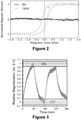
- the magnetization versus magnetic field curve of the as-deposited disks shows no obvious hysteresis (i.e., OFF magnetism in the as-prepared state) (see Figure 2 ).
- a clear hysteresis loop is observed after subjecting the FeO x to -50 V (ON state), with a magnetic moment at saturation of 24 ⁇ emu.
- the magnetic state of the pristine FeO x disks (before applying any voltage) can be varied and hysteresis loops with low saturation magnetization can also be obtained.
- application of the negative voltage also induces a measurable increase of the magnetic moment.
- the effects of the negative voltage can be reversed by applying a positive voltage (of certain magnitude and time duration).
- the changes in magnetic moment are not absolute or discrete, but can take intermediate values depending on the time and voltage value that is used.
- This analog variation of the magnetization, with applied voltage and time can be the basis for the use of this technology and procedure in neuromorphic computing.
- X-ray photoelectron spectroscopy can be used. Given the need for ultra-high vacuum environment during XPS experiments, the effect of the magnetoelectric actuation has to be analysed ex-situ, after voltage has been applied and outside the electrochemical cell setup.
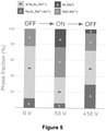
- the XPS spectra reveal that the pristine FeO x disks consist of a mixture of iron oxide phases (hematite, wüstite and magnetite). The relative percentages of the different oxides are given in Figure 5 .
- the second main implementation of the first aspect of the present invention relates to the use of voltage to induce transitions in the reversal mode of patterned ferromagnetic structures, at room temperature, when deposited onto ferroelectric substrate (piezo-strain mediated magnetic transitions). More specifically, a transition from ferromagnetic states (square hysteresis loops with two clear remanent magnetization values, i.e. coherent rotation reversal mode) to states with zero net remanent magnetization (for example, vortex-like states) or states with very low remanent magnetization (for example, C-states or S-states) can be induced in Fe 75 Al 25 (at.
- the effects of voltage are not governed by ion migration (magneto-ionics) but, instead, they are mediated by piezostrain, via the coupling between the highly magnetostrictive FeAl phase and the ferroelectric substrate S2.
- no liquid electrolyte is used during magnetoelectric measurements.
- the electrical contacts are made directly at both sides of the PMN-32PT crystals, in this case by corresponding silver paste portions Ls, and the Fe 75 Al 25 disks are electrically charged through the underlying Cu conductive layer Lc (see Figure 6 ).
- Magnetic hysteresis loops are recorded by magneto-optic Kerr effect (MOKE), focusing the laser spot (which is about 25 ⁇ m in diameter) directly on top of the patterned disk of interest.
- the magnetoelectric device of the first aspect of the present invention consists of electrically interconnecting different groups of dots (i.e. of patterned structures or magnetoelectric elements Me) of one or more arrays, in different ways, so that magnetoelectric actuation (either magneto-ionic or strain-mediated) can be performed selectively to a single dot or patterned structure Me, groups of patterned structures Me or the whole array of patterned structures Me.
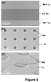
- Figure 8 shows two sub-arrays of patterned disks Me, grown onto a Cu seed layer Lc of a substrate S1, S2, separated by a rectangular region with no deposited Cu (and with no disks Me) - a shadow mask was used for such a purpose.
- Electric contact can be made either to the upper or to the bottom sub-arrays of disks Me, or to both simultaneously.
- the presence of an electrically insulating spacer region (the surface of the Si/SiO 2 substrate S1, S2 is insulating unless it is metallized with Cu), allows for this selective electrical actuation.
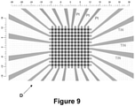
- FIG. 9 Another embodiment of the magnetoelectric device of the first aspect of the present invention is related to the implementation of crossbar arrays of interconnected memory units ( Figure 9 ). These arrays can be fabricated using a sequential deposition method that combines standard optical lithography techniques. First, a layer of photoresist is spin-coated on the Si surface and then exposed under ultraviolet light in a Micro-Writer lithography system. A developer is used to dissolve the exposed areas, where a conductive layer of e.g. TiN is grown by reactive sputtering. Next, the unexposed areas are lifted off using acetone, thus resulting in the patterning of the bottom electrodes.
- a sequential deposition method that combines standard optical lithography techniques. First, a layer of photoresist is spin-coated on the Si surface and then exposed under ultraviolet light in a Micro-Writer lithography system. A developer is used to dissolve the exposed areas, where a conductive layer of e.g. TiN is grown by reactive sputtering. Next, the
- the layers of interest i.e., those comprised in the multi-stack memory units
- the pads of bottom electrode e.g., TiN plus the multi-stack comprising the magnetic layers
- an upper Pt electrode is patterned employing similar optical lithography protocols, defining the perpendicular crossbar structure.
- FIG. 10 A further embodiment of the magnetoelectric device of the first aspect of the present invention is shown in Figure 10 .
- a solid-state magnetoelectric storage device is depicted, which consists of an ordered array of micro/nano-scale transition-metal oxide (MO x ) interconnected dots Me arranged over a substrate S1 S2, each of the interconnected dots Me being in direct contact with an oxygen getter/donor layer (e.g., Gd, which will become GdO x upon voltage application) deposited below these dots Me to either give or accept oxygen upon voltage application (depending on the voltage polarity).
- Gd oxygen getter/donor layer
- These dots Me can be electrically connected using different paths, through corresponding metal elements Bm, forming various possible circuits.
- An electrically insulating material In is arranged between and under the dots Me.
- voltage ( ⁇ V) can be applied only to pre-selected dots Me belonging to an activated path (e.g., circuit '6').
- ⁇ V voltage
- the pre-selected disks will undergo transitions from antiferromagnetic to ferromagnetic states (magneto-ionic effect) or from coherent rotation to vortex-like hysteresis loops (strain-mediated magnetoelectric effect).
- voltage is directly used to write "ON" or "OFF" bits of information in each magnetic memory unit.
- the magnetoelectric device D of the first aspect of the invention for the embodiment shown in Figure 10
- the presence or absence of magnetic signal in the memory units including magnetoelectric elements Me of the embodiment of Figure 10 can be read using a magnetic sensor.
- This effect constitutes the basis of a secure keycard (similar to those employed to open the doors of rooms in a hotel).
- the sensor reads the ON state (with either positive or negative saturation magnetization) as "1" and the OFF state as "0". Since these states are written with voltage and not with magnetic field, this offers an enhanced degree of robustness compared to conventional magnetic keycards, which can be easily demagnetized in the proximity of a permanent magnet.
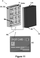
- a similar device architecture can be utilized to implement prototypes of smart cards in high-security identification or credit cards CC ( Figure 11 ), by means of a spatially-resolved magnetic sensor R with spatial resolution, and having an insulating substrate S3 with a metal layer Lm facing the memory units.
- Figure 12 shows an embodiment of the magnetoelectric device D of the first aspect of the present invention, for implementing a magnetoelectric MRAM (ME-RAM) device comprising a plurality of memory units including respective magnetoelectric elements Me for implementing their free layers, and the electrical interconnection between those magnetoelectric elements or disks Me (in this case using a crossbar geometry).
- ME-RAM magnetoelectric MRAM
- the magnetic properties of the free layer contained in each memory unit are manipulated using voltage instead of high-intensity spin-polarized currents, as opposed to STT-RAM devices.
- the saturation magnetization of the free layer can be either increased or decreased with voltage (eventually it can be brought to zero) if the mechanism governing the magnetoelectric actuation is the ion migration or, alternatively, the reversal mode of the free layer can be changed from coherent rotation to vortex (or vice versa ) if its magnetoelectric behavior is strain-mediated. In all cases, this will result in changes in the magnetoresistance which can be detected during the reading operation of the ME-RAM. As a final application, it is proposed that such ME-RAM devices can be used as "physical unclonable function" (PUF) systems for enhanced data protection hardware solutions.
- PAF physical unclonable function
Landscapes
- Engineering & Computer Science (AREA)
- Computer Hardware Design (AREA)
- Hall/Mr Elements (AREA)
- Mram Or Spin Memory Techniques (AREA)
Abstract
- a magnetoelectric element (Me); and
- an electric voltage source (PS) configured and arranged to induce on the magnetoelectric element (Me), at least at room temperature, ON-OFF states and OFF-ON states magnetic transitions, by applying or removing determined electric voltages, wherein at said ON state the magnetoelectric element (Me) shows permanent and net magnetization.
Description
- The present invention generally relates, in a first aspect, to a magnetoelectric device adapted to undergo ON-OFF states and OFF-ON states magnetic transitions, and more particularly to a magnetoelectric device made to provide said transitions by ferromagnetic to/from antiferromagnetic transitions.
- A second aspect of the present invention relate to different uses of the magnetoelectric device of the first aspect of the present invention, including a use for implementing a data security device, and uses for information and communications technologies, including neuromorphic computing and/or stochastic data storage and/or stochastic data processing.
- To be at the forefront of advanced and sustainable economies in our modern society, it is not only crucial to develop breakthrough technologies but also to translate them into new products, processes and services. Increasing industrial competitiveness while fulfilling energy, environment, security and other related demands is a central objective, which is intrinsically linked to technological advances and, ultimately, to scientific progress. Internet and digital technologies are transforming our world at a vertiginous speed. Big Data is a clear example, challenging information technology to an unprecedented extent, not only in terms of storage capacity needs but also from processing speed, robustness/stability and energy-efficiency as well as confidentiality, integrity and data availability aspects. According to International Data Corporation (IDC) [https://www.idc.com/abouf], Big Data is surpassing the €175 billion market in 2020 (€112 billion in 2016) and, by 2025, around 180 trillion GB of information will be generated [https://www.forbes.com/sites/gilpress/2017/01/20/6-predictions-for-the-203-billion-big-data-analytics-marketl#3b00b3572083]. Regarding data security, a Wipro study reported that, based on public disclosures, more than 2.7 billion data files are being stolen every year, doubling the total amount of data breaches during the preceding year [https:llwww.wipro.com/].
- Information technology deals with the storage, retrieval and manipulation of data in electronic devices, such as computers. Computers share a common architecture, known as the Von Neumann architecture, based on a storage hierarchy approach and built around the central processing unit (CPU), which constitutes the electronic circuitry (i.e., processor). Next to the CPU is located the so-called random-access memory (RAM), or primary memory, a sub-device which allows data items to be rapidly stored and manipulated. The mass storage sub-device (e.g., the hard disk drive, HDD), designed to exclusively store large amounts of information in partial detriment of processing speed, is placed further away [D. A. Patterson, J. L. Hennessy, in Computer Organization and Design: The Hardware/Software Interface (5th edition, Elsevier Inc., Amsterdam, 2014 )]. Nowadays, even though semiconductor-based RAMs, such as dynamic or static RAMs (DRAMs and SRAMs, respectively) are mainly used [https://techinsights.com/], magnetoresistive RAMs (MRAMs) are already on the market, foreseeing magnetically-actuated RAMs as the next generation of these primary memories. In contrast to dynamical and static memories, MRAMs are non-volatile, fast enough to compete with static RAMs, more power efficient and allow for higher storage densities. MRAM technology is based on spintronics (spin-based electronics), incorporating spin (i.e., magnetism) as an additional degree of freedom to electronic charge [S. Bhatti et al., Spintronics based random access memory: a review, Mater. Today 20 (2017) 530-548]. The MRAM variant based on spin transfer torque (STT-MRAMs) is so far the most promising in terms of energy-efficiency [K. L. Wang et al., Low-power non-volatile spintronic memory: STT-RAM and beyond, J. Phys. D: Appl. Phys. 46 (2013) 074003].
- Although the Von Neumann computer architecture has been widely and successfully used for more than five decades, further device scaling (computing volume and complexity scaling) is hindered due to power and data processing speed considerations. The time and energy spent transporting data between the memory and the processor (i.e., along the communication bus) has become a bottleneck for new progress in the field. A new paradigm for data storage and processing, inspired by the operating principles of neurons in the brain, has emerged in recent years [C. D. James et al., A historical survey of algorithms and hardware architectures for neural-inspired and neuromorphic computing applications, Biol. Inspir. Cogn. Arc. 19 (2017) 49-64]. So-called "neuromorphic computing" is based on the assembly of a myriad of low-power electrically interconnected computing elements (neurons) and adaptive memory units (artificial synapses) which can operate in parallel via spikes and the generation of synaptic weights, outperforming traditional computer systems both in terms of capacity and speed. Both digital and analogic neuromorphically-engineered integration systems have been proposed. One of the most efficient geometric arrangements of computing elements is the use of crossbar arrays. Different types of physical devices and principles of operation have been proposed in order to operate each memory unit. Perhaps the most extended is resistive switching (memristor-based synaptic devices), which takes advantage of drastic changes in the electric resistance of two-terminal dielectric materials under the action of strong electric fields or currents [D. lelmini, H. S. Philip Wong, In-memory computing with resistive switching devices, Nat. Electron. 1 (2018) 333-343]. Such a change is non-volatile and reversible and it has been utilized in the so-called resistive-RAMs (RRAMs). Some drawbacks of this type of memories are: (i) relatively high energy dissipation, in the form of Joule heating effects, during writing or encoding of information, (ii) uncontrolled fluctuations which renders increased read error outputs, (iii) difficulties to program memristors with a negative synaptic weight (inhibitory postsynaptic potential) and (iv) lack of understanding of the physical mechanisms responsible for the drastic change in conductivity [R. Mishra et al., Oxygen-migration-based spintronic device emulating a biological synapse, Phys. Rev. Appl. 11 (2019) 054065]. Some of these drawbacks, as will be described below, can be overcome by using magnetoelectric, instead of resistive, memory units in voltage-driven MRAM architectures.
- Returning to conventional (Von Neumann) computer architectures, data storage and manipulation rely on magnetic HDDs and either electrically- or magnetically-actuated RAMs, respectively [S. D. Bader, S. S. P. Parkin, Spintronics. Rev. Condens. Matter. Phys. 1 (2010) 71-88]. According to the International Roadmap for Devices and Systems [https://irds.ieee.org/editions/2018], the optimization of such devices is considered a long-term challenge in electronics. In particular, these systems are ultimately controlled by electric currents (i.e., magnetic fields through electromagnetic induction and/or spin-polarized electric currents via STT), involving a significant energy waste by heat dissipation through the Joule effect. The energy needed to switch a memory unit in a toggle MRAM is around 1 pJ, while that in a STT-RAM is 10-1 pJ. This is one and two orders of magnitude larger than the writing energy/bit in dynamic (DRAM) and static (SRAM) devices, respectively [H. Cai et al., High performance MRAM with spin-transfer-torque and voltage-controlled magnetic anisotropy effects, Appl. Sci. 7 (2017) 929].
- Alternatively, electric field control of magnetism (by converse magnetoelectric effect) is a fundamentally different approach towards the implementation of ultralow-heat-dissipation memories (with writing energies/bit down to 10-6 pJ) [S. Manipatruni et al., Scalable energy-efficient magnetoelectric spin-orbit logic, Nature 565 (2019) 35-42]. In this case, voltage is applied through an insulating layer (with an infinite resistance) and, therefore, electrons remain virtually static (leakage current flowing across the structure is nearly zero). As a result, this type of memories is highly efficient from an energy consumption viewpoint. Recently, magnetoelectric approaches have been realized in numerous classes of materials and architectures where an efficient modulation of various parameters, such as coercivity, magnetic moment, magnetic anisotropy, remanent magnetization, exchange bias, topological spin structures, etc. has been achieved [C. Navarro-Senent et al., Electrolyte-gated magnetoelectric actuation: Phenomenology, materials, mechanisms, and prospective applications, APL Mater. 7 (2019) 030701 ; A. Molinari et al., Voltage-control of magnetism in all-solid-state and solid/liquid magnetoelectric composites, Adv. Mater. 31 (2019) 1806662]. Some of the reported effects, such as the modulation of magnetization with voltage, has been proposed for neuromorphic computing [R. Mishra et al., Oxygen-migration-based spintronic device emulating a biological synapse, Phys. Rev. Appl. 11 (2019) 054065]. However, most of the research done so far has been focused on continuous films. Magnetoelectric studies on ordered arrays of patterned structures, in which different voltages can be applied to different memory units, have not been performed so far and are essential to bridge fundamental research to marketable devices.
- Electric-field control of magnetism has primarily relied on the following strategies: (i) the use of single-phase multiferroic materials with intrinsic magnetoelectric coupling [W. Eerenstein et al., Multiferroic and magnetoelectric materials, Nature 442 (2006) 759-765], (ii) electric charge accumulation in ferromagnetic metals [M. Weisheit et al., Electric field-induced modification of magnetism in thin-film ferromagnets, Science 315 (2007) 349-351 ;_ A. Quintana et al., Voltage-induced coercivity reduction in nanoporous alloy films: a boost toward energy-efficient magnetic actuation. Adv. Funct. Mater. 27 (2017) 1701904] or semiconductors [H. Ohno et al., Electric-field control of ferromagnetism. Nature 408 (2000) 944-946] (i.e., direct electric-field effect) and (iii) piezostrain-mediated effects through inverse magnetostriction in ferromagnetic/ferroelectric heterostructures [M. Liu et al., Giant electric field tuning of magnetic properties in multiferroic ferrite/ferroelectric heterostructures, Adv. Mater. 19 (2009) 1826-1831]. However, the implementation of these approaches in marketable devices, such as magnetoelectric random access memories (ME-RAMs) [M. Bibes, A. Barthélémy, Towards a magnetoelectric memory nature materials. Nat. Mater. 7 (2008) 425-426], is hampered by several factors. Intrinsic multiferroics are scarce and show weak magnetoelectric coupling [N. Izyumskaya et al., Oxides, oxides, and more oxides: High-κ oxides, ferroelectrics, ferromagnetics, and multiferroics, Crit. Rev. Solid State Mater. Sci. 34 (2009) 89-179]. Due to the limited electric-field screening length in metallic ferromagnetic materials (within the Thomas-Fermi screening length which is roughly 5 Å), electronic charging is only observed in ultrathin films (2-3 nm), thus imposing strong fabrication/processing challenges [I. V. Ovchinnikov, K. L. Wang, Theory of electric-field-controlled surface ferromagnetic transition in metals, Phys. Rev. B 79 (2009) 020402(R )]. Finally, strain-mediated artificial multiferroic ferromagnetic/ferroelectric heterostructures suffer from clamping effects with the substrate, severely limiting the achievable strains and, thus, the potential magnetic modulation, and yielding mechanical failure [Y. Wang et al., Multiferroic magnetoelectric composite nanostructures. NPG Asia Mater. 2 (2010) 61-68].
- In recent years, voltage-induced ion motion in magnetic materials (magneto-ionics) has revolutionized electric-field control of magnetism, since this mechanism may allow for a voltage-driven modulation of magnetic properties to an extent not reached by any of the aforementioned magnetoelectric means. Magneto-ionics also overcomes some of the drawbacks of the other magnetoelectric mechanisms, such as the clamping effects or film thickness limitation. In some materials an applied electric field induces ion migration of, e.g., O2- [A. Quintana et al., Voltage-controlled ON-OFF ferromagnetism at room temperature in a single metal oxide film, ACS Nano. 12 (2018) 10291; S. Robbennolt et al., Electric Field Control of Magnetism in Iron Oxide Nanoporous Thin Films, ACS Appl. Mater. Interfaces. 11 (2019) 37338-37346 ; U. Bauer et al., Magneto-ionic control of interfacial magnetism, Nat. Mater. 14 (2015) 174-181], Li+ [Q. Zhang et al., Lithium-Ion Battery Cycling for Magnetism Control, Nano Lett. 16 (2016) 583-587 ; S. Dasgupta et al., Toward on and off magnetism: reversible electrochemistry to control magnetic phase transitions in spinel ferrites, Adv. Funct. Mater. 26 (2016) 7507-7515], H+ [A. J. Tan et al., Magneto-ionic control of magnetism using a solid-state proton pump, Nat. Mater. 18 (2019) 35-41 ; M. Gößler et al., Magneto-ionic switching of superparamagnetism, Small 15 (2019) 1904523] or F- [S. Vasala et al., Reversible tuning of magnetization in a ferromagnetic Ruddlesden-Popper-type manganite by electrochemical fluoride-ion intercalation, Adv. Electron. Mater. 6 (2020) 1900974] back and forth between the material of interest and an ion source/sink, depending on the voltage polarity. Diffusion of ions is associated with a change in the oxidation state of the metal, thus leading to large changes in magnetization. In the extreme case, one can induce ON/OFF magnetic switching, generating (ON) or suppressing (OFF) ferromagnetism at will, with voltage [A. Quintana et al., Voltage-controlled ON-OFF ferromagnetism at room temperature in a single metal oxide film, ACS Nano. 12 (2018) 10291 ; A. Molinari et al., Voltage-Controlled On/Off Switching of Ferromagnetism in Manganite Supercapacitors, Adv. Mater. 30 (2018) 1703908].
- So far, such an effect has been observed at room temperature in only a very limited number of systems, such as non-patterned continuous Co3O4 thin films [A. Quintana et al., Voltage-controlled ON-OFF ferromagnetism at room temperature in a single metal oxide film, ACS Nano. 12 (2018) 10291], for a magnetoelectric element which adopts the OFF state by becoming paramagnetic, and which are therefore not applicable to implement ME-RAMs.
- ON-OFF ferromagnetism at low temperatures was also achieved in La0.74Sr0.26MnO3 films by electrochemical (pseudo-capacitance) doping [A. Molinari et al., Voltage-Controlled On/Off Switching of Ferromagnetism in Manganite Supercapacitors, Adv. Mater. 30 (2018) 1703908 ]. Other complex oxide heterostructures, such as perovskite SrCoO3-δ actuated through an ionic liquid gate, also require of low temperature (<225 K) to enable ON/OFF magnetic switching [N. Lu et al., Electric-field control of tristate phase transformation with a selective dual-ion switch, Nature. 546 (2017) 124-128]. High-temperature (>470 K) voltage-assisted oxidation of ultrathin (0.7 nm) Co layers in contact with GdOx underlayers has also been used to suppress magnetization [C. Bi et al., Reversible control of Co magnetism by voltage-induced oxidation, Phys. Rev. Lett. 113 (2014) 267202]. A maximum of up to 70% change of the magnetization has been observed in ZnFe2O4 films at room temperature by electrochemistry-driven Li-ion exchange [S. Dasgupta et al., Toward on and off magnetism: reversible electrochemistry to control magnetic phase transitions in spinel ferrites, Adv. Funct. Mater. 26 (2016) 7507-7515].
- Full ON/OFF switching of the magnetization at room temperature in low-dimensional systems (in view of applications to miniaturized devices) remains rather elusive. For instance, it has been realized via Li+ intercalation/deintercalation in α-Fe2O3 nanoparticles loaded onto a Cu foil cathode in a lithium ion battery [Q. Zhang et al., Lithium-Ion Battery Cycling for Magnetism Control, Nano Lett. 16 (2016) 583-587]. During lithiation, the device becomes magnetized due to an electrochemical reaction between the iron oxide and Li+ which results in partial conversion of oxide into metallic Fe. The effect is fully reversed during the de-lithiation process. Yet, α-Fe2O3 particles larger than 1 µm undergo irreversible changes in magnetism and cannot sustain large lithium intercalation [Q. Zhang et al., Lithium-Ion Battery Cycling for Magnetism Control, Nano Lett. 16 (2016) 583-587 ; D. Larcher et al., Effect of Particle Size on Lithium Intercalation into α-Fe2O3, J. Electrochem. Soc. 150 (2003) A133-A139]. Remarkably, almost complete ON/OFF switching was recently reported for β-FeOOH nanoplatelets in an alkaline Li-based electrolyte at room temperature [M. Nichterwitz et al., Voltage-controlled on switching and manipulation of magnetization via the redox transformation of β-FeOOH nanoplatelets, J. Phys. D. Appl. Phys. 53 (2020) 084001] and in electrodeposited Fe naturally covered by a thin layer of FeOx tested in aqueous KOH solution [K. Duschek et al., All-electrochemical voltage-control of magnetization in metal oxide/metal nanoislands, J. Mater. Chem. C. 6 (2018) 8411-8417]. In the former case, application of negative voltage results in the reduction of virtually non-magnetic β-FeOOH to metallic Fe giving rise to magnetization; however, the platelet nanostructure is collapsed after first voltage cycle and cannot be recovered anymore. In the latter case, a modulation of magnetization (up to 86 %) was achieved by applying moderate voltages. However, the presence of a ferrimagnetic component in the starting FeOx material precludes initial OFF magnetism. In these examples, the low-dimensional materials under investigation have random shapes or are disposed randomly onto a surface, thus precluding their use in interconnected ordered memory arrays.
- Besides magneto-ionics, strain-mediated converse magneto-electric effects have been sometimes used to induce large changes in the magnetic properties of materials. A drastic voltage-controlled ON-OFF ferromagnetism at room temperature has only been achieved by tuning the antiferromagnetic-to-ferromagnetic metamagnetic transition of FeRh thin films [R. O. Cherifi et al., Electric-field control of magnetic order above room temperature, Nat. Mater. 13 (2014) 345-351] or the superparamagnetic blocking temperature of Ni nanoparticles [H. K. D. Kim et a/., Magnetoelectric control of superparamagnetism, Nano Lett. 13 (2013) 884-888], in both cases through the coupling to underlying ferroelectric substrates. Voltage has been also used to induce a reorientation of the magnetic easy-axis in arrays of dipolarly coupled elliptical FeGa dots (preserving coherent rotation modes of magnetization reversal) [H. Ahmad et al., Electric field control of magnetic states in isolated and dipole-coupled FeGa nanomagnets delineated on a PMN-PT substrate, Nanotechnology 26 (2015) 401001]. Transition from coherent rotation mode (i.e., square hysteresis loops with two remanent magnetization states) to vortex-like hysteresis loops (with zero or virtually zero remanent magnetization) has been only predicted theoretically for a single dot [Q. Sheng et a/., Phase diagrams of magnetic state transformations in multiferroic composites controlled by size, shape and interfacial coupling strain, AIP Adv. 7 (2017) 105221] and not demonstrated experimentally. Moreover, the case of an array of dots remains from theoretical and experimental viewpoints unexplored. It is, therefore, necessary to provide an alternative to the state of the art which covers the gaps found therein, by providing a magnetoelectric device which indeed induces ON-OFF magnetic switching at room temperature, of a kind which make it suitable for being used, among others, as a ME-RAM.
- To that end, the present invention relates, in a first aspect, to a magnetoelectric device, comprising:
- a magnetoelectric element; and
- an electric voltage source configured and arranged to induce on said magnetoelectric element, at least at room temperature, ON-OFF states and OFF-ON states magnetic transitions, by applying or removing determined electric voltages, wherein at said ON state the magnetoelectric element shows permanent and net magnetization, i.e. ferromagnetism.
- In contrast to the systems known in the prior art, in the system of the present invention, in a characterizing manner, the magnetoelectric element is configured and arranged to be, at said induced OFF state, completely antiferromagnetic or partially antiferromagnetic (i.e., with some traces of ferromagnetism) but with a magnetization below 50 emu/cm3. This makes it suitable for implementing a ME-RAM.
- As stated above, the magnetoelectric device of the first aspect of the present invention operates (i.e., is made to undergo the ON-OFF and OFF-ON states magnetic transitions) at least at room temperature, which means that it is made to operate with no external o extrinsic applied additional heating or cooling, and specifically from room temperature up to a temperature below the Néel temperature of the antiferromagnetic element.
- For a first main implementation, the magnetoelectric element and the electric voltage source are configured and arranged to induce the above mentioned ON-OFF states and OFF-ON states magnetic transitions by phase transformations caused by a voltage-driven ion migration mechanism.
- For some embodiments of said first main implementation, the magnetoelectric element is made of an oxide or nitride of iron, nickel, ternary nickel-cobalt or ternary cobalt-manganese.
- According to some of those embodiments, the magnetoelectric element is an iron oxide comprising, when no voltage is applied thereto, hematite, wüstite or a mixture of hematite and wüstite iron oxide phases (antiferromagnetic), and wherein the magnetoelectric element and the electric voltage source are configured and arranged to induce phase transformations including:
- for the ON state, metallic iron (ferromagnetic) and/or maghemite (ferrimagnetic) and/or magnetite (ferrimagnetic); and
- for the OFF state, said hematite and wüstite iron oxide phases, and no metallic iron, no magnetite and no maghemite or a rather small fraction of metallic iron and magnetite providing said magnetization below 50 emu/cm3 (in the form of superparamagnetic clusters).
- For an embodiment of the first main implementation, the magnetoelectric element is in the form of a dense layer (i.e., a non-porous layer) of thickness between 2 and 200 nm, and the magnetization device further comprises:
- an electrically conducting substrate or a substrate with an electrically conducting buffer/seed layer; and
- a top electrode configured and arranged to act as ion reservoir and/or electric contact.
- According to different embodiments of the first main implementation, the electric voltage source is configured and arranged to applying the determined electric voltages to the magnetoelectric element for example via a condenser-like configuration, by means of other schemes, such as transistor-like configurations, in which case the magnetoelectric element would act itself as source and drain of current.
- For a second main implementation of the magnetoelectric device of the first aspect of the present invention, the magnetoelectric device further comprises a ferroelectric substrate supporting the magnetoelectric element, and the magnetoelectric element and the electric voltage source are configured and arranged to induce said ON-OFF states and OFF-ON states magnetic transitions by reversal mode changes caused by a mechanism providing a voltage-driven piezostrain-mediated coupling between the ferroelectric substrate and the magnetoelectric element, wherein said reversal mode changes refer to changes from/to a ferromagnetic state with multi- or single-domain state, for said ON state, to/from a state with a closure domain with minimal squareness (MR/MS.100% where MR is the remanent magnetization and Ms is the saturation magnetization) below 10% for said OFF state.
- According to an embodiment of said second main implementation, the magnetoelectric element has an any form (e.g., oval, circular, square, rectangular...), the ferromagnetic state corresponds to either a multi- or a single-domain state (i.e., non-constricted hysteresis loop), and wherein said state with minimal squareness is a flux-closure domain structure where magnetization is symmetrically distributed in-plane with respect to the flux-closure domain structure core, allowing for a maximum remanent magnetization MR of 10% of the saturation magnetization Ms in case the flux-closure domain structure core is offset from the magnetoelectric element centre.
- Preferably, the above mentioned full-closure domain structure is a vortex or similar full-closure domain structure.
- For an embodiment of the second main implementation, the electric voltage source is configured and arranged to apply said determined electric voltages perpendicularly (i.e., out-of-plane poling) to a surface of the ferroelectric substrate facing said magnetoelectric element and to the plane of the magnetoelectric element, for example via a condenser-like configuration, through which an in-plane voltage-induced strain is produced under the out-of-plane application of said determined electric voltages.
- According to an embodiment of the second main implementation, the magnetoelectric element is made of a soft ferromagnetic material with a coercivity below 200 Oe having a large polycrystalline magnetostrictive constant λ above 100 ppm.
- For a variant of said embodiment, said soft ferromagnetic material is a Fe-based alloy, such as FeAI.
- For an embodiment of the second main implementation, the electric voltage source is configured and arranged to provide an initial out-of-plane electrical poling of the ferroelectric substrate to make the magnetoelectric element prepared for being induced to the OFF state when a determined electric voltage is applied by the electric voltage source.
- The magnetoelectric element has respective X and Y lateral dimensions below 30 µm (any shape) and a thickness equal or larger than 2 nm, for an embodiment of the second main implementation of the magnetoelectric device of the first aspect of the present invention.
- The magnetoelectric device of the first aspect of the invention comprises for an embodiment:
- an ordered array of magnetoelectric elements including the magnetoelectric element described above (for any of its implementations and embodiments) and further magnetoelectric elements which are as said magnetoelectric element; and
- an interconnection arrangement electrically connecting at least part of the magnetoelectric elements of the array and the electric voltage source, wherein the electric voltage source is configured and arranged to induce on at least some of the magnetoelectric elements, at room temperature, said ON-OFF states and OFF-ON states magnetic transitions, by selectively applying or removing said determined electric voltages thereto.
- For a variant of said embodiment, the magnetoelectric device implements a magnetoelectric random access memory (ME-RAM) device, wherein each of the magnetoelectric elements of the ordered array is a free or pinned layer of a corresponding magnetic tunnel junction of a memory unit.
- For some embodiments, the magnetoelectric element is in the form of a continuous film. However for other embodiments, it is in the form patterned "dots", or separate elements, forming part of the above mentioned array by being electrically interconnected using different paths. This allows for the use of this effect to implement ME-RAM device architectures (e.g., crossbar geometries) suitable for several uses.
- A second aspect of the present invention relates to different uses of the magnetoelectric device of the first aspect of the present invention:
- to implement a data security device using either a rigid or a flexible substrate or support for the magnetoelectric element or array of magnetoelectric elements, or
- for information and communications technologies, including neuromorphic computing and/or stochastic data storage and/or stochastic data processing.
- The uses related to neuromorphic computing or stochastic data storage and processing (i.e., computing) benefit from the above mentioned ME-RAM device architectures.
- Specifically, the stochastic data processing can benefit from local variations in the threshold voltage values to induce ON-OFF magneto-ionic transitions in the different memory units due to uncontrolled (i.e., not completely reproducible) manufacturing processes. This is the working principle of devices for "physical unclonable functions" and "true random number generators" [T. McGrath et al., A PUF taxonomy, Appl. Phys. Rev. 6 (2019) 011303], which constitute ultra-secure hardware solutions compared to conventional software cryptographic methods, which utilize complex algorithms that require additional data and increased power consumption, thus potentially reducing cost-efficiency.
- In the following some preferred embodiments of the invention will be described with reference to the enclosed figures. They are provided only for illustration purposes without however limiting the scope of the invention.
-
Figure 1 : Experimental setup used to measure the magnetoelectric properties of the patterned structures or dots, i.e. of magnetoelectric elements Me, of the magnetoelectric device D (called "sample" below) of the first aspect of the present invention, in liquid configuration. It consists of a home-made electrochemical cell, where the sample/device D acts as working electrode and a Pt spiral as counter electrode WPt. An anhydrous electrolyte EI (propylene carbonate with dissolved Na+ ions) is utilized to prevent oxidation of the sample D upon electrical polarization of the solution. This electrolyte EI also allows the formation of the electric double layer when voltage is applied. The setup can be assembled with a vibrating sample magnetometer Vb (to measure the magnetic signal of the whole array of dots Me while voltage is applied) or with a magneto-optic Kerr effect setup, to locally measure a single dot. -
Figure 2 : Normalized hysteresis loops from FeOx disks in the as-prepared state (ΔV = 0 V) and while applying a voltage ΔV = -50 V. -
Figure 3 : Variation of the normalized magnetization with time for FeOx during two consecutive cycles, first applying ΔV = -10 V (to induce the "ON" state) and then ΔV = +10V (to induce the OFF state). -
Figure 4 : X-ray photoelectron spectroscopy (XPS) spectra of the 2p3/2 Fe peaks of the FeOx disks in (a) the pristine state (ΔV = 0 V), (b) after applying a negative voltage (ΔV = -50 V) and (c) after subsequently applying a positive voltage (ΔV = 50 V). The experimental data has been fitted using the convolution of the peaks corresponding to different Fe oxide phases (hematite, magnetite, wüstite) and metallic Fe. -
Figure 5 : Quantitative assessment of the phase percentages (α-Fe2O3 : hematite, Fe3O4: magnetite, Fe1-yOy: wüstite, Fe0: metallic iron), obtained from the fits of the X-ray photoelectron spectroscopy (XPS) spectra, of FeOx disks, at 0 V (OFF state), after applying ΔV = -50 V ("ON" state) and after subsequently applying ΔV = +50 V (partial-OFF state, in which 80% of the magnetization was removed during the time a given voltage was applied). -
Figure 6 : (a) Scanning electron microscopy (SEM) image of a Fe75Al25 (at. %) dense disk grown onto a lead magnesium niobate-lead titanate [PbMg1/3Nb2/3O3-32% PbTiO3 (PMN-PT)] [001] single crystal substrate S2 by sputtering, in combination with optical lithography and photoresist lift off. (b) Custom-made setup (magneto-optic Kerr effect, MOKE) used to measure the hysteresis loops of this disk while applying different voltage values. -
Figure 7 : Hysteresis loops of a Fe75Al25 (at. %) disk (25 µm in diameter), grown onto a [110]-oriented ferroelectric lead magnesium niobate-lead titanate [PbMg1/3Nb2/3O3-32% PbTiO3 (PMN-PT)] single crystal, at (a) ΔV = 0 V (pristine state), (b) ΔV = + 50 V and (c) ΔV = + 100 V. In the latter two cases, the sample was first brought to ΔV = -200 V to pole the ferroelectric substrate. Note that while two different remanent states are clearly observed at 0 V and +50 V, only one state is obtained after applying ΔV = +100 V (i.e., corresponding to a vortex-like hysteresis loop). -
Figure 8 : (a) Scanning electron microscopy (SEM) image showing two arrays of interconnected dots (through the underlying electrically conductive Cu layer) separated by a trench for electrical isolation (in which the Si/SiO2 substrate was not coated with Cu, i.e. using a shadow mask). (b) Top SEM view image of an enlarged area of one of the magnetoelectrically actuated array of dots. (c) Tilted SEM view of the array of magnetoelectrically actuated disks. -
Figure 9 : Crossbar arrangement that can be prepared using a sequential deposition method that combines standard optical lithography techniques. -
Figure 10 : A solid-state magnetoelectric storage device which consists of an ordered array of micro/nano-scale transition-metal oxide (MOx) interconnected dots, each of them in direct contact with an oxygen getter/donor layer (e.g., Gd, which will become GdOx upon voltage application) deposited below these dots to either provide or accept oxygen upon voltage application (depending on the voltage polarity). The dots can be electrically connected in a combinatorial fashion, i.e., using different paths, therefore, forming a number of possible circuits. Voltage (ΔV) will be applied only to pre-selected dots belonging to an activated path (e.g., circuit '6'). By applying ΔV, the pre-selected disks will undergo transitions from antiferromagnetic (or paramagnetic) to ferromagnetic (or ferrimagnetic) states. Metal paths can be made of metals such as Cu, Pt or Au. -
Figure 11 : Concept/configuration of a voltage-actuated multi-element security memory device to be used in anti-counterfeiting technologies (e.g., smart chips in credit cards). -
Figure 12 : (a) Schematic drawing of the magnetoelectric device of the first aspect of the present invention implementing a magnetic random-access memory (MRAM) device in which each magnetic unit consists of a magnetic tunnel junction coupled to complementary-metal-oxide semiconductor (CMOS) transistor. (b) Writing operation principle in a voltage-driven MRAM using the magnetoelectric element of the magnetoelectric device as a free layer in the magnetic tunnel junctions. - In the present section some working embodiments of the present invention will be described with reference to the Figures.
- In a previous section first and second main implementations of the magnetoelectric device of the first aspect of the present invention have been described, based on two different physical mechanisms, to induce ON-OFF (or OFF-ON) magnetic transitions, at room temperature, in one or more magnetoelectric elements, by means of applying or removing determined electric voltages, of given polarities.
- In the present section, those first and second main implementations will be described with more detail, and experiments carried out by the present inventors will be described for both of said first and second main implementations.
- For the first main implementation, as stated above, voltage is used to induce a controlled migration of ions (e.g., oxygen or nitrogen) in one or more magnetic elements of certain metal oxide or nitride patterned structures. This effect is referred to as "magneto-ionics". Such migration induces a transition from antiferromagnetic phases (with zero or negligible magnetic moment) to ferromagnetic phases (with a certain net magnetization that can be tuned with voltage). The effect is here demonstrated in FeOx disks (8 µm in diameter) prepared from continuous films grown by evaporation induced self-assembly and subsequently patterned by optical lithography plus selective etching. The typical thickness of the FeOx layer is 100 nm and it exhibits a 25% porosity degree with an average ligament size of around 20 nm. Magnetoelectric measurements are performed using vibrating sample magnetometry (VSM) while applying voltage in a home-made setup. Anhydrous propylene carbonate, a liquid electrolyte, is used as a means to generate an electric double layer which conformally coats the surface when voltage is applied. Starting from a virtually non-magnetic OFF state (magnetization below the threshold of detection), a clear ferromagnetic-like hysteresis loop (ON state) is obtained when a negative voltage is applied. The generated signal is proportional to the applied voltage and progressively increases with the time voltage is applied. Such ON state can be reversed (magnetism can be essentially deleted) by subsequently applying a sufficiently high positive voltage. The cycling process can be repeated several times, demonstrating reasonably good endurance. This magnetic phase transition is related to oxygen migration (from the sample to the electrolyte during negative voltage and vice versa for positive voltage), which causes reversible phase transformations. In particular, metallic iron phase is formed when negative voltage is applied (providing finite magnetization), while it reoxidizes when positive voltage is applied (reducing the magnetization). Slight changes in the amounts of oxides depending on the applied voltage and time can be quantified by using X-ray photoelectron spectroscopy. Similar effects can be induced in sputtered CoN and FeN, where magneto-ionics is driven by voltage-induced nitrogen ion migration, instead of oxygen migration.
- In the first main implementation of the first aspect of the present invention, a magneto-ionic OFF-ON effect is demonstrated in circular disks consisting of FeOx. First, FeOx films are prepared by the evaporation-induced self-assembly (EISA) method. Then, the films are patterned by optical lithography followed by chemical etching. The complete technical details and processing conditions are as follows. To grow the films, a sol-gel is first obtained by dissolving 400 mg FeCl2·4H2O and 380 mg citric acid (1:1 molar ratio) in 10 ml of ethanol absolute. The solution is stirred for 48 h at 500 rpm at room temperature. Sputtered Pt thin film (70 nm in thickness) onto Si chips serve as substrates for the FeOx films deposition. The Si/Pt substrates are cleaned in oxygen plasma and soaked in 0.4 M KOH solution (1:1 water:ethanol mixed solvent) for 5 min to increase sol-gel wettability. The FeOx thin film is obtained by dip-coating technique, using a withdrawal rate of 300 mm/min in a
Coater 5 AC from id Lab at room temperature and 50 % relative humidity. After dip-coating, the samples are promptly transferred to the hot plate at 100°C to assist fast solvent evaporation. Accumulated thickness of the FeOx layers can be realized by iterating this cycle, i.e., for 100 nm thick film, the dipping process is repeated 3 times gently annealing the layers at 100°C for 10 min after dipping. As a final step, the samples are annealed at 600°C for 3 h in air atmosphere to crystalize the oxide. Patterning of the arrays of FeOx microdisks are then obtained by a conventional microfabrication sequence, consisting in photolithography and selective chemical etching processes. The photoresist patterned as an array of circles of 10 µm in diameter is used as mask in the chemical etching. Wet chemical etchant consists in concentrated HCI acid (12 M) and is able to remove unmasked FeOx in approximately 14 min, selectively, i.e., both photoresist and Pt film are unaffected. The photoresist mask is, then, removed by immersing the samples in dimethyl sulfoxide (DMSO) for 45 min, followed by a final gentle rising in acetone, isopropanol and Milli-Q water. In a similar fashion, arrays of CoN and FeN disks can be prepared combining e.g. reactive sputtering and optical lithography processing or sequence. - For the embodiment of this first main implementation shown in
Figure 1 , in-situ magnetoelectric measurements are performed on the assembly of patterned dots (i.e., magnetoelectric elements Me) using a MicroSense (LOT-QuantumDesign) Vibrating Sample Magnetometer (VSM) (seeFigure 1 ), for by magnetic field coils C1, C2 to provide a vibration to the device D according to direction Vb. The voltage is applied using an Agilent B2902A power supply PS through a home-made electrochemical cell attached to the VSM holder. The FeOx sample, or device D, acts as a cathode and the contact is made to an underlying Pt seed layer (not shown) of a substrate S1, in this case via an accessible electrically conductive pad P. A Pt wire is the counter electrode WPt. The two electrodes are placed parallel to each other in a small Eppendorf® tube (1 mL) filled with the anhydrous propylene carbonate (PC) solution (Figure 1 ). The electrolyte is externally treated with metallic Na to eliminate any trace of water and thus contains a small fraction of Na+ (ca. 5 ppm) and OH- ions. No other salts are added. Magnetic hysteresis loops are recorded in-plane after the voltage (negative or positive) is applied to the sample for 1 h. Apart from the FeOx samples, magnetic hysteresis loops are also recorded for the spare Si/Pt substrate immersed in the electrochemical cell containing of the same components as in the case of FeOx for recording a reference signal. Subsequently, the substrate contribution is subtracted from the magnetic hysteresis loops of FeOx. The magnetization versus magnetic field curve of the as-deposited disks shows no obvious hysteresis (i.e., OFF magnetism in the as-prepared state) (seeFigure 2 ). Conversely, a clear hysteresis loop is observed after subjecting the FeOx to -50 V (ON state), with a magnetic moment at saturation of 24 µemu. It is worth mentioning that, depending on the EISA conditions, the magnetic state of the pristine FeOx disks (before applying any voltage) can be varied and hysteresis loops with low saturation magnetization can also be obtained. In that case, application of the negative voltage also induces a measurable increase of the magnetic moment. Remarkably, the effects of the negative voltage can be reversed by applying a positive voltage (of certain magnitude and time duration).Figure 3 shows how the saturation magnetization of the FeOx disks can be increased and then decreased, two times consecutively, applying alternating values of negative (ΔV = -10 V) and positive (ΔV = +10 V), respectively. The changes in magnetic moment are not absolute or discrete, but can take intermediate values depending on the time and voltage value that is used. This analog variation of the magnetization, with applied voltage and time, can be the basis for the use of this technology and procedure in neuromorphic computing. - To unravel the mechanism which governs the OFF-ON magnetic transition, X-ray photoelectron spectroscopy (XPS) can be used. Given the need for ultra-high vacuum environment during XPS experiments, the effect of the magnetoelectric actuation has to be analysed ex-situ, after voltage has been applied and outside the electrochemical cell setup. The XPS spectra (
Figure 4 ) reveal that the pristine FeOx disks consist of a mixture of iron oxide phases (hematite, wüstite and magnetite). The relative percentages of the different oxides are given inFigure 5 . Note that while magnetite (which is ferrimagnetic in bulk form) is present in the as-prepared state, no hysteresis loop can be measured at ΔV = 0 V (Figure 2 ), suggesting that this phase is mainly in the form of small superparamagnetic nanoclusters, so that they do not give rise to any hysteresis and the attainable magnetization is below the detection limit of the technique. Remarkably, XPS spectra reveal that when a negative voltage (ΔV = -50 V) is applied, a fraction of metallic iron forms. This can explain the emergence of the ferromagnetic behavior (ON state). After positive voltage (ΔV = +50 V) is applied, metallic iron re-oxidizes, and the FeOx disks become again a mixture of oxide phases. Note that XPS is a surface-sensitive technique, so the overall phase percentages given inFigure 5 should be taken with certain caution. - The second main implementation of the first aspect of the present invention relates to the use of voltage to induce transitions in the reversal mode of patterned ferromagnetic structures, at room temperature, when deposited onto ferroelectric substrate (piezo-strain mediated magnetic transitions). More specifically, a transition from ferromagnetic states (square hysteresis loops with two clear remanent magnetization values, i.e. coherent rotation reversal mode) to states with zero net remanent magnetization (for example, vortex-like states) or states with very low remanent magnetization (for example, C-states or S-states) can be induced in Fe75Al25 (at. %) disks (25 µm in diameter, layer thickness around 50 nm, dense) deposited onto a lead magnesium niobate-lead titanate [PbMg1/3Nb2/3O3-32% PbTiO3 (PMN-PT)] [001] single crystal by sputtering. Imprinting of ferroelectric domains to the ferromagnetic Fe75Al25 layer is at the heart of the observed effects.
- For the second main implementation of the magnetoelectric device of the first aspect of the present invention, the magnetoelectric behaviour of an array of dense (non-mesoporous) Fe75Al25 (at.%) disks (20 µm in diameter, 50 nm in thickness), implementing magnetoelectric elements Me, grown onto a PMN-32PT ferroelectric [100] single-crystalline substrate S2, is investigated. These disks Me are grown by sputtering and a thin Cu film Lc is used as seed layer over the substrate S2. Patterning is performed by optical lithography and subsequent wet chemical etching, using a process analogous to that reported in the first embodiment (in this case with acetone and for two minutes in an ultra-sounds bath). In this case, the effects of voltage are not governed by ion migration (magneto-ionics) but, instead, they are mediated by piezostrain, via the coupling between the highly magnetostrictive FeAl phase and the ferroelectric substrate S2. Here, no liquid electrolyte is used during magnetoelectric measurements. Instead, the electrical contacts are made directly at both sides of the PMN-32PT crystals, in this case by corresponding silver paste portions Ls, and the Fe75Al25 disks are electrically charged through the underlying Cu conductive layer Lc (see
Figure 6 ). Magnetic hysteresis loops are recorded by magneto-optic Kerr effect (MOKE), focusing the laser spot (which is about 25 µm in diameter) directly on top of the patterned disk of interest. A square hysteresis loop, with two possible remanent magnetization states ("ON +" and "ON -") is obtained in the pristine disks at ΔV = 0 V. Out-of-plane electrical poling of the ferroelectric is then performed by applying a strong negative voltage (ΔV = -200 V). Remarkably, after doing so, the hysteresis loops that are recorded while applying positive voltages (e.g., at ΔV = +50 V or ΔV = +100 V), tend to change their shape, losing their squareness and becoming progressively more constricted as the positive voltage value is increased (seeFigure 7 ). While "ON +" and "ON -" states with lower remanent magnetization are obtained at ΔV = +50 V, a vortex-like hysteresis loop (with zero remanent magnetization, "OFF" state) is measured at ΔV = +100 V. These results show the strong influence of voltage-controlled strain on the obtained magnetic properties. Here, opposite to the magneto-ionic case described in the first embodiment, no phase transformations are induced by voltage. Instead, the existing piezostrain causes a change in the magnetization reversal mode of the patterned structures. Remarkably, the pristine Fe75Al25 disks are probably already under the influence of strain due to the underlying ferroelectric substrate, which has a spontaneous ferroelectric polarization. When voltage is applied, new domains form in the ferroelectric substrate, which change the strain state in the Fe75Al25 disks, resulting in the observed constriction of the hysteresis loops. In this context, coupling between the ferroelectric domains in PMN-32 (molar %) PT and the ferromagnetic state in Fe75Al25 is envisaged. Interestingly, similar to the first embodiment, the effect of voltage can also be reversed here. Hysteresis loops with two remanent states can be recovered if the applied positive voltage is further increased (e.g., ΔV = +200 V) or by bringing the disks back to 0 V. The maximum constriction is thus obtained around ΔV = +100 V, which is the coercive voltage of the substrate. A notable aspect of this second embodiment is that here the magnetoelectric effects are rather instantaneous (as opposed to magneto-ionics, which required applying each voltage value for several minutes). - For an embodiment of any of the above described first and second main implementations, the magnetoelectric device of the first aspect of the present invention consists of electrically interconnecting different groups of dots (i.e. of patterned structures or magnetoelectric elements Me) of one or more arrays, in different ways, so that magnetoelectric actuation (either magneto-ionic or strain-mediated) can be performed selectively to a single dot or patterned structure Me, groups of patterned structures Me or the whole array of patterned structures Me. In the simplest example,
Figure 8 shows two sub-arrays of patterned disks Me, grown onto a Cu seed layer Lc of a substrate S1, S2, separated by a rectangular region with no deposited Cu (and with no disks Me) - a shadow mask was used for such a purpose. Electric contact can be made either to the upper or to the bottom sub-arrays of disks Me, or to both simultaneously. The presence of an electrically insulating spacer region (the surface of the Si/SiO2 substrate S1, S2 is insulating unless it is metallized with Cu), allows for this selective electrical actuation. In this way, for example, one can induce an "ON state" in the upper sub-array of dots Me and an "OFF state" in the bottom sub-array of dots Me. Or, even more interestingly, two different ON states (with different magnetization) can be obtained in the two sub-arrays of disks Me by applying different voltage values to them. This selective actuation is the basis for the utilization of this magnetoelectric effect in practical applications such as neuromorphic computing or data security devices. - Another embodiment of the magnetoelectric device of the first aspect of the present invention is related to the implementation of crossbar arrays of interconnected memory units (
Figure 9 ). These arrays can be fabricated using a sequential deposition method that combines standard optical lithography techniques. First, a layer of photoresist is spin-coated on the Si surface and then exposed under ultraviolet light in a Micro-Writer lithography system. A developer is used to dissolve the exposed areas, where a conductive layer of e.g. TiN is grown by reactive sputtering. Next, the unexposed areas are lifted off using acetone, thus resulting in the patterning of the bottom electrodes. Subsequently, the layers of interest (i.e., those comprised in the multi-stack memory units) are sputtered. Then, the pads of bottom electrode (e.g., TiN plus the multi-stack comprising the magnetic layers) are exposed through lithography and wet etching. Finally, an upper Pt electrode is patterned employing similar optical lithography protocols, defining the perpendicular crossbar structure. - A further embodiment of the magnetoelectric device of the first aspect of the present invention is shown in
Figure 10 . In this case, a solid-state magnetoelectric storage device is depicted, which consists of an ordered array of micro/nano-scale transition-metal oxide (MOx) interconnected dots Me arranged over a substrate S1 S2, each of the interconnected dots Me being in direct contact with an oxygen getter/donor layer (e.g., Gd, which will become GdOx upon voltage application) deposited below these dots Me to either give or accept oxygen upon voltage application (depending on the voltage polarity). These dots Me can be electrically connected using different paths, through corresponding metal elements Bm, forming various possible circuits. An electrically insulating material In is arranged between and under the dots Me. For example, as illustrated inFigure 10 , voltage (ΔV) can be applied only to pre-selected dots Me belonging to an activated path (e.g., circuit '6'). By applying ΔV between the selected metal element(s) Bm and a metal layer Lm attached to an insulating substrate S3, the pre-selected disks will undergo transitions from antiferromagnetic to ferromagnetic states (magneto-ionic effect) or from coherent rotation to vortex-like hysteresis loops (strain-mediated magnetoelectric effect). In this device, voltage is directly used to write "ON" or "OFF" bits of information in each magnetic memory unit. - One of the possible uses of the second aspect of the present invention, for which the magnetoelectric device D of the first aspect of the invention, for the embodiment shown in
Figure 10 , is used. In this case the presence or absence of magnetic signal in the memory units including magnetoelectric elements Me of the embodiment ofFigure 10 can be read using a magnetic sensor. This effect constitutes the basis of a secure keycard (similar to those employed to open the doors of rooms in a hotel). The sensor reads the ON state (with either positive or negative saturation magnetization) as "1" and the OFF state as "0". Since these states are written with voltage and not with magnetic field, this offers an enhanced degree of robustness compared to conventional magnetic keycards, which can be easily demagnetized in the proximity of a permanent magnet. Different passwords can be established in these keycards, each of them activating or deactivating different collections of pre-selected memory units with voltage. A similar device architecture can be utilized to implement prototypes of smart cards in high-security identification or credit cards CC (Figure 11 ), by means of a spatially-resolved magnetic sensor R with spatial resolution, and having an insulating substrate S3 with a metal layer Lm facing the memory units. - Finally,
Figure 12 shows an embodiment of the magnetoelectric device D of the first aspect of the present invention, for implementing a magnetoelectric MRAM (ME-RAM) device comprising a plurality of memory units including respective magnetoelectric elements Me for implementing their free layers, and the electrical interconnection between those magnetoelectric elements or disks Me (in this case using a crossbar geometry). Here, the magnetic properties of the free layer contained in each memory unit (the so-called magnetic tunnel junction, MTJ) are manipulated using voltage instead of high-intensity spin-polarized currents, as opposed to STT-RAM devices. The saturation magnetization of the free layer can be either increased or decreased with voltage (eventually it can be brought to zero) if the mechanism governing the magnetoelectric actuation is the ion migration or, alternatively, the reversal mode of the free layer can be changed from coherent rotation to vortex (or vice versa) if its magnetoelectric behavior is strain-mediated. In all cases, this will result in changes in the magnetoresistance which can be detected during the reading operation of the ME-RAM. As a final application, it is proposed that such ME-RAM devices can be used as "physical unclonable function" (PUF) systems for enhanced data protection hardware solutions. By setting all memory units to the same state, variations in the magnetoresistance would still be detectable when comparing the readings from different MTJs, due to uncontrolled microstructural variations within the layers not addressable during the manufacturing process. This would allow to set a series of "challenges-responses" pairs, a procedure known as PUF authentication [T. McGrath et al., A PUF taxonomy, Appl. Phys. Rev. 6 (2019) 011303]. Another property that could serve as the basis for these PUF ME-RAMs is the critical threshold voltage to induce the ON-OFF (or OFF-ON) magnetic transitions, which will be slightly different for each magnetic memory unit due to manufacturing variations. By applying a voltage very close to the nominal threshold voltage, a stochastic (i.e., random) transition between ON and OFF states (or between states with different magnetization) will occur. This could be the principle for stochastic data processing or stochastic computing. - A person skilled in the art could introduce changes and modifications in the embodiments described without departing from the scope of the invention as it is defined in the attached claims.
Claims (15)
- A magnetoelectric device (D), comprising:- a magnetoelectric element (Me); and- an electric voltage source (PS) configured and arranged to induce on said magnetoelectric element (Me), at least at room temperature, ON-OFF states and OFF-ON states magnetic transitions, by applying or removing determined electric voltages, wherein at said ON state the magnetoelectric element (Me) shows permanent and net magnetization;characterized in that the magnetoelectric element (Me) is configured and arranged to be, at said induced OFF state, completely antiferromagnetic or partially antiferromagnetic but with a magnetization below 50 emu/cm3.
- The magnetoelectric device (D) according to claim 1, wherein the magnetoelectric element (Me) and the electric voltage source (PS) are configured and arranged to induce said ON-OFF states and OFF-ON states magnetic transitions by phase transformations caused by a voltage-driven ion migration mechanism.
- The magnetoelectric device (D) according to claim 2, wherein the magnetoelectric element (Me) is made of an oxide or nitride of iron, nickel, ternary nickel-cobalt or ternary cobalt-manganese.
- The magnetoelectric device (D) according to claim 3, wherein the magnetoelectric element (Me) is an iron oxide comprising, when no voltage is applied thereto, hematite, wüstite or a mixture of hematite and wüstite iron oxide phases, and wherein the magnetoelectric element (Me) and the electric voltage source (PS) are configured and arranged to induce phase transformations including:- for the ON state, metallic iron and/or magnetite; and- for the OFF state, said hematite and wüstite iron oxide phases, and no metallic iron, no magnetite and no maghemite or a rather small fraction of metallic iron and magnetite providing said magnetization below 50 emu/cm3.
- The magnetization device according to any of claim 2 to 4, wherein said magnetoelectric element (Me) is in the form of a dense layer of thickness between 2 and 200 nm, and the magnetization device (D) further comprises:- an electrically conducting substrate (S1) or a substrate (S1) with an electrically conducting buffer/seed layer (Lc); and- a top electrode (P) configured and arranged to act as ion reservoir and/or electric contact.
- The magnetoelectric device (D) according to claim 1, further comprising a ferroelectric substrate (S2) supporting the magnetoelectric element (Me), and wherein the magnetoelectric element (Me) and the electric voltage source (PS) are configured and arranged to induce said ON-OFF states and OFF-ON states magnetic transitions by reversal mode changes caused by a mechanism providing a voltage-driven piezostrain-mediated coupling between the ferroelectric substrate (S2) and the magnetoelectric element (Me), wherein said reversal mode changes refer to changes from/to a ferromagnetic state with multi- or single-domain state, for said ON state, to/from a state with a closure domain with minimal squareness below 10% for said OFF state.
- The magnetoelectric device (D) according to claim 6, wherein said ferromagnetic state corresponds to either a multi- or a single-domain state, and wherein said state with minimal squareness is a flux-closure domain structure where magnetization is symmetrically distributed in-plane with respect to the flux-closure domain structure core, allowing for a maximum remanent magnetization MR of 10% of the saturation magnetization Ms in case the flux-closure domain structure core is offset from the magnetoelectric element (Me) centre.
- The magnetization device according to claim 6 or 7, wherein said electric voltage source (PS) is configured and arranged to apply said determined electric voltages perpendicularly to a surface of the ferroelectric substrate (S2) facing said magnetoelectric element (Me) and to the plane of the magnetoelectric element (Me) via a condenser-like configuration through which an in-plane voltage-induced strain is produced under the out-of-plane application of said determined electric voltages.
- The magnetization device according to any of claims 6 to 8, wherein the magnetoelectric element (Me) is made of a soft ferromagnetic material with a coercivity below 200 Oe having a large polycrystalline magnetostrictive constant λ above 100 ppm.
- The magnetization device according to claim 9, wherein said soft ferromagnetic material is a Fe-based alloy.
- The magnetization device according to any of claims 6 to 10, wherein the electric voltage source (PS) is configured and arranged to provide an initial out-of-plane electrical poling of the ferroelectric substrate (S2) to make the magnetoelectric element (Me) prepared for being induced to the OFF state when a determined electric voltage is applied by the electric voltage source (PS).
- The method according to any of claims 6 to 11, wherein said magnetoelectric element (Me) has respective X and Y lateral dimensions below 30 µm and a thickness equal or larger than 2 nm.
- The magnetoelectric device (D) according to any of the previous claims, comprising:- an ordered array of magnetoelectric elements (Me) including said magnetoelectric element (Me) and further magnetoelectric elements which are as said magnetoelectric element (Me); and- an interconnection arrangement electrically connecting at least part of the magnetoelectric elements (Me) of the array and the electric voltage source (PS), wherein the electric voltage source (PS) is configured and arranged to induce on at least some of the magnetoelectric elements (Me), at room temperature, said ON-OFF states and OFF-ON states magnetic transitions, by selectively applying or removing said determined electric voltages thereto.
- The magnetoelectric device (D) according to claim 13, wherein it implements a magnetoelectric random access memory (ME-RAM) device, wherein each of said magnetoelectric elements (Me) of the ordered array is a free or pinned layer of a corresponding magnetic tunnel junction of a memory unit.
- Use of the magnetoelectric device (D) according to any of the previous claims:- to implement a data security device using either a rigid or a flexible substrate or support for the magnetoelectric element (Me) or array of magnetoelectric elements (Me), or- for information and communications technologies, including neuromorphic computing and/or stochastic data storage and/or stochastic data processing.
Priority Applications (3)
| Application Number | Priority Date | Filing Date | Title |
|---|---|---|---|
| ES20382628T ES3001458T3 (en) | 2020-07-14 | 2020-07-14 | A magnetoelectric device and uses of the magnetoelectric device |
| EP20382628.4A EP3940702B1 (en) | 2020-07-14 | 2020-07-14 | A magnetoelectric device and uses of the magnetoelectric device |
| PCT/EP2021/060062 WO2022012790A1 (en) | 2020-07-14 | 2021-04-19 | A magnetoelectric device and uses of the magnetoelectric device |
Applications Claiming Priority (1)
| Application Number | Priority Date | Filing Date | Title |
|---|---|---|---|
| EP20382628.4A EP3940702B1 (en) | 2020-07-14 | 2020-07-14 | A magnetoelectric device and uses of the magnetoelectric device |
Publications (3)
| Publication Number | Publication Date |
|---|---|
| EP3940702A1 true EP3940702A1 (en) | 2022-01-19 |
| EP3940702B1 EP3940702B1 (en) | 2024-11-27 |
| EP3940702C0 EP3940702C0 (en) | 2024-11-27 |
Family
ID=72039485
Family Applications (1)
| Application Number | Title | Priority Date | Filing Date |
|---|---|---|---|
| EP20382628.4A Active EP3940702B1 (en) | 2020-07-14 | 2020-07-14 | A magnetoelectric device and uses of the magnetoelectric device |
Country Status (3)
| Country | Link |
|---|---|
| EP (1) | EP3940702B1 (en) |
| ES (1) | ES3001458T3 (en) |
| WO (1) | WO2022012790A1 (en) |
Cited By (1)
| Publication number | Priority date | Publication date | Assignee | Title |
|---|---|---|---|---|
| CN118778914A (en) * | 2024-09-13 | 2024-10-15 | 青岛海存微电子有限公司 | Semiconductor memory devices |
Family Cites Families (2)
| Publication number | Priority date | Publication date | Assignee | Title |
|---|---|---|---|---|
| JP4568926B2 (en) * | 1999-07-14 | 2010-10-27 | ソニー株式会社 | Magnetic functional element and magnetic recording apparatus |
| US8054677B2 (en) * | 2008-08-07 | 2011-11-08 | Seagate Technology Llc | Magnetic memory with strain-assisted exchange coupling switch |
-
2020
- 2020-07-14 EP EP20382628.4A patent/EP3940702B1/en active Active
- 2020-07-14 ES ES20382628T patent/ES3001458T3/en active Active
-
2021
- 2021-04-19 WO PCT/EP2021/060062 patent/WO2022012790A1/en not_active Ceased
Non-Patent Citations (40)
| Title |
|---|
| A. J. TAN ET AL.: "Magneto-ionic control of magnetism using a solid-state proton pump", NAT. MATER., vol. 18, 2019, pages 35 - 41 |
| A. MOLINARI ET AL.: "Voltage-Controlled On/Off Switching of Ferromagnetism in Manganite Supercapacitors", ADV. MATER., vol. 30, 2018, pages 1703908 |
| A. MOLINARI: "Voltage-control of magnetism in all-solid-state and solid/liquid magnetoelectric composites", ADV. MATER., vol. 31, 2019, pages 1806662 |
| A. QUINTANA ET AL.: "Voltage-controlled ON-OFF ferromagnetism at room temperature in a single metal oxide film", ACS NANO, vol. 12, 2018, pages 10291 |
| A. QUINTANA ET AL.: "Voltage-induced coercivity reduction in nanoporous alloy films: a boost toward energy-efficient magnetic actuation", ADV. FUNCT. MATER., vol. 27, 2017, pages 1701904 |
| C. BI ET AL.: "Reversible control of Co magnetism by voltage-induced oxidation", PHYS. REV. LETT., vol. 113, 2014, pages 267202 |
| C. D. JAMES: "A historical survey of algorithms and hardware architectures for neural-inspired and neuromorphic computing applications", BIOL. INSPIR. COGN. ARC., vol. 19, 2017, pages 49 - 64 |
| C. NAVARRO-SENENT: "Electrolyte-gated magnetoelectric actuation: Phenomenology, materials, mechanisms, and prospective applications", APL MATER., vol. 7, 2019, pages 030701 |
| D. LARCHER ET AL.: "Effect of Particle Size on Lithium Intercalation into a-Fe 0", J. ELECTROCHEM. SOC., vol. 150, 2003, pages A 133 - A 139 |
| D. LELMINIH. S. PHILIP WONG: "In-memory computing with resistive switching devices", NAT. ELECTRON, vol. 1, 2018, pages 333 - 343 |
| H. AHMAD ET AL.: "Electric field control of magnetic states in isolated and dipole-coupled FeGa nanomagnets delineated on a PMN-PT substrate", NANOTECHNOLOGY, vol. 26, 2015, pages 401001 |
| H. CAI ET AL.: "igh performance MRAM with spin-transfer-torque and voltage-controlled magnetic anisotropy effects", APPL. SCI., vol. 7, 2017, pages 929 |
| H. K. D. KIM: "Magnetoelectric control of superparamagnetism", NANO LETT., vol. 13, 2013, pages 884 - 888 |
| H. OHNO ET AL.: "Electric-field control of ferromagnetism", NATURE, vol. 408, 2000, pages 944 - 946 |
| I. V. OVCHINNIKOVK. L. WANG: "Theory of electric-field-controlled surface ferromagnetic transition in metals", PHYS. REV. B, vol. 79, 2009, pages 020402 |
| JIANG M ET AL: "Electrochemical control of the phase transition of ultrathin FeRh films", APPLIED PHYSICS LETTERS, A I P PUBLISHING LLC, US, vol. 108, no. 20, 16 May 2016 (2016-05-16), XP012207848, ISSN: 0003-6951, [retrieved on 19010101], DOI: 10.1063/1.4950973 * |
| K. DUSCHEK ET AL.: "All-electrochemical voltage-control of magnetization in metal oxide/metal nanoislands", J. MATER. CHEM. C., vol. 6, 2018, pages 8411 - 8417 |
| K. L. WANG: "Low-power non-volatile spintronic memory: STT-RAM and beyond", J. PHYS. D: APPL. PHYS., vol. 46, 2013, pages 074003 |
| M. BIBESA. BARTHELEMY: "Towards a magnetoelectric memory nature materials", NAT. MATER., vol. 7, 2008, pages 425 - 426 |
| M. GO FILER ET AL.: "Magneto-ionic switching of superparamagnetism", SMALL, vol. 15, 2019, pages 1904523 |
| M. LIU ET AL.: "Giant electric field tuning of magnetic properties in multiferroic ferritelferroelectric heterostructures", ADV. MATER., vol. 19, 2009, pages 1826 - 1831 |
| M. NICHTERWITZ ET AL.: "Voltage-controlled on switching and manipulation of magnetization via the redox transformation of /3-FeOO/-/ nanoplatelets", J. PHYS. D. APPL. PHYS., vol. 53, 2020, pages 084001 |
| M. WEISHEIT: "Electric field-induced modification of magnetism in thin-film ferromagnets", SCIENCE, vol. 315, 2007, pages 349 - 351 |
| N. IZYUMSKAYA ET AL.: ", Oxides, oxides, and more oxides: High-K oxides, ferroelectrics, ferromagnetics, and multiferroics", CRIT. REV. SOLID STATE MATER. SCI., vol. 34, 2009, pages 89 - 179 |
| N. LU ET AL.: "Electric-field control of tristate phase transformation with a selective dual-ion switch", NATURE, vol. 546, 2017, pages 124 - 128 |
| NAVARRO-SENENT CRISTINA ET AL: "Electrolyte-gated magnetoelectric actuation: Phenomenology, materials, mechanisms, and prospective applications", APL MATERIALS, AMERICAN INSTITUTE OF PHYSICS, 2 HUNTINGTON QUADRANGLE, MELVILLE, NY 11747, vol. 7, no. 3, 6 March 2019 (2019-03-06), XP012242075, DOI: 10.1063/1.5080284 * |
| Q. SHENG: "Phase diagrams of magnetic state transformations in multiferroic composites controlled by size, shape and interfacial coupling strain", AIP ADV., vol. 7, 2017, pages 105221 |
| Q. ZHANG ET AL.: "Lithium-Ion Battery Cycling for Magnetism Control", NANO LETT., vol. 16, 2016, pages 583 - 587 |
| R. MISHRA ET AL.: "Oxygen-migration-based spintronic device emulating a biological synapse", PHYS. REV. APPL., vol. 11, 2019, pages 054065 |
| R. O. CHERIFI: "Electric-field control of magnetic order above room temperature", NAT. MATER., vol. 13, 2014, pages 345 - 351 |
| S. BHATTI: "Spintronics based random access memory: a review", MATER. TODAY, vol. 20, 2017, pages 530 - 548 |
| S. D. BADERS. S. P. PARKIN, SPINTRONICS. REV. CONDENS. MATTER. PHYS., vol. 1, 2010, pages 71 - 88 |
| S. DASGUPTA ET AL.: "Toward on and off magnetism: reversible electrochemistry to control magnetic phase transitions in spinel ferrites", ADV. FUNCT. MATER., vol. 26, 2016, pages 7507 - 7515 |
| S. MANIPATRUNI ET AL.: "Scalable energy-efficient magnetoelectric spin-orbit logic", NATURE, vol. 565, 2019, pages 35 - 42 |
| S. ROBBENNOLT ET AL.: "Electric Field Control of Magnetism in Iron Oxide Nanoporous Thin Films", ACS APPL. MATER. INTERFACES, vol. 11, 2019, pages 37338 - 37346 |
| S. VASALA ET AL.: "Reversible tuning of magnetization in a ferromagnetic Ruddlesden-Popper-type manganite by electrochemical fluoride-ion intercalation", ADV. ELECTRON. MATER., vol. 6, 2020, pages 1900974 |
| T. MCGRATH ET AL.: "A PUF taxonomy", APPL. PHYS. REV., vol. 6, 2019, pages 011303 |
| U. BAUER ET AL.: "Magneto-ionic control of interfacial magnetism", NAT. MATER., vol. 14, 2015, pages 174 - 181 |
| V. WANG ET AL.: "Multiferroic magnetoelectric composite nanostructures", NPG ASIA MATER., vol. 2, 2010, pages 61 - 68 |
| W EERENSTEIN: "Multiferroic and magnetoelectric materials", NATURE, vol. 442, 2006, pages 759 - 765 |
Cited By (1)
| Publication number | Priority date | Publication date | Assignee | Title |
|---|---|---|---|---|
| CN118778914A (en) * | 2024-09-13 | 2024-10-15 | 青岛海存微电子有限公司 | Semiconductor memory devices |
Also Published As
| Publication number | Publication date |
|---|---|
| EP3940702B1 (en) | 2024-11-27 |
| EP3940702C0 (en) | 2024-11-27 |
| ES3001458T3 (en) | 2025-03-05 |
| WO2022012790A1 (en) | 2022-01-20 |
Similar Documents
| Publication | Publication Date | Title |
|---|---|---|
| Guo et al. | Ferroic tunnel junctions and their application in neuromorphic networks | |
| Luo et al. | Voltage-controlled skyrmion memristor for energy-efficient synapse applications | |
| CN101896976B (en) | High speed low power magnetic devices based on current induced spin-momentum transfer | |
| JP5360774B2 (en) | Magnetization control method, information storage method, information storage element, and magnetic functional element | |
| JP5909223B2 (en) | High-speed low-power magnetic device based on current-induced spin-momentum transfer | |
| KR100754930B1 (en) | MRM element of voltage controlled magnetization inversion recording method and method of recording and reading information using the same | |
| CN100507591C (en) | Synthetic antiferromagnetic structure for magnetoelectronics devices | |
| CN109952662B (en) | Spin device, method of operating the same, and method of manufacturing the same | |
| US8023317B2 (en) | Magnetic random access memory with dual spin torque reference layers | |
| US9196336B2 (en) | Storage cell, storage device, and magnetic head | |
| EP2903020B1 (en) | Storage element, storage device, and magnetic head | |
| US9385309B2 (en) | Smooth seed layers with uniform crystalline texture for high perpendicular magnetic anisotropy materials | |
| Dong et al. | Field-Free Current-Induced Switching of L 10-Fe Pt Using Interlayer Exchange Coupling for Neuromorphic Computing | |
| EP3961632A1 (en) | Magnetic tunnel junction comprising an inhomogeneous granular free layer and associated spintronic devices | |
| Ren et al. | Efficient spin–orbit torque switching in a perpendicularly magnetized Heusler alloy MnPtGe single layer | |
| Namiki et al. | Room-temperature manipulation of magnetization angle, achieved with an all-solid-state redox device | |
| Tang et al. | Electric-field control of perpendicularly magnetized ferrimagnetic order and giant magnetoresistance in multiferroic heterostructures | |
| EP3940702B1 (en) | A magnetoelectric device and uses of the magnetoelectric device | |
| CN112968125A (en) | Device for driving magnetic flip magnetic moment by spin orbit torque without external field and preparation method | |
| Liu et al. | Field-free Spin–Orbit Torque Perpendicular Magnetization Switching Induced by Metallic Multilayers | |
| Locatelli et al. | Magnetic and ferroelectric memories | |
| Bertacco et al. | New trends in magnetic memories | |
| Rajib | Voltage control of interfacial magnetism for energy-efficient skyrmion-based memory and neuromorphic computing | |
| Ameziane | Solid-state lithium magnetoionics for voltage control of magnetic phenomena | |
| Jadhav et al. | Nanoferrites in memory devices |
Legal Events
| Date | Code | Title | Description |
|---|---|---|---|
| PUAI | Public reference made under article 153(3) epc to a published international application that has entered the european phase |
Free format text: ORIGINAL CODE: 0009012 |
|
| STAA | Information on the status of an ep patent application or granted ep patent |
Free format text: STATUS: THE APPLICATION HAS BEEN PUBLISHED |
|
| AK | Designated contracting states |
Kind code of ref document: A1 Designated state(s): AL AT BE BG CH CY CZ DE DK EE ES FI FR GB GR HR HU IE IS IT LI LT LU LV MC MK MT NL NO PL PT RO RS SE SI SK SM TR |
|
| STAA | Information on the status of an ep patent application or granted ep patent |
Free format text: STATUS: REQUEST FOR EXAMINATION WAS MADE |
|
| 17P | Request for examination filed |
Effective date: 20220714 |
|
| RBV | Designated contracting states (corrected) |
Designated state(s): AL AT BE BG CH CY CZ DE DK EE ES FI FR GB GR HR HU IE IS IT LI LT LU LV MC MK MT NL NO PL PT RO RS SE SI SK SM TR |
|
| GRAP | Despatch of communication of intention to grant a patent |
Free format text: ORIGINAL CODE: EPIDOSNIGR1 |
|
| STAA | Information on the status of an ep patent application or granted ep patent |
Free format text: STATUS: GRANT OF PATENT IS INTENDED |
|
| RIC1 | Information provided on ipc code assigned before grant |
Ipc: H10N 50/10 20230101ALI20240620BHEP Ipc: H10N 50/80 20230101ALI20240620BHEP Ipc: H10B 61/00 20230101ALI20240620BHEP Ipc: G11C 11/16 20060101ALI20240620BHEP Ipc: G11C 11/15 20060101AFI20240620BHEP |
|
| INTG | Intention to grant announced |
Effective date: 20240705 |
|
| GRAS | Grant fee paid |
Free format text: ORIGINAL CODE: EPIDOSNIGR3 |
|
| GRAA | (expected) grant |
Free format text: ORIGINAL CODE: 0009210 |
|
| STAA | Information on the status of an ep patent application or granted ep patent |
Free format text: STATUS: THE PATENT HAS BEEN GRANTED |
|
| AK | Designated contracting states |
Kind code of ref document: B1 Designated state(s): AL AT BE BG CH CY CZ DE DK EE ES FI FR GB GR HR HU IE IS IT LI LT LU LV MC MK MT NL NO PL PT RO RS SE SI SK SM TR |
|
| REG | Reference to a national code |
Ref country code: GB Ref legal event code: FG4D |
|
| REG | Reference to a national code |
Ref country code: CH Ref legal event code: EP |
|
| REG | Reference to a national code |
Ref country code: IE Ref legal event code: FG4D |
|
| REG | Reference to a national code |
Ref country code: DE Ref legal event code: R096 Ref document number: 602020041988 Country of ref document: DE |
|
| U01 | Request for unitary effect filed |
Effective date: 20241223 |
|
| U07 | Unitary effect registered |
Designated state(s): AT BE BG DE DK EE FI FR IT LT LU LV MT NL PT RO SE SI Effective date: 20250121 |
|
| PG25 | Lapsed in a contracting state [announced via postgrant information from national office to epo] |
Ref country code: HR Free format text: LAPSE BECAUSE OF FAILURE TO SUBMIT A TRANSLATION OF THE DESCRIPTION OR TO PAY THE FEE WITHIN THE PRESCRIBED TIME-LIMIT Effective date: 20241127 Ref country code: IS Free format text: LAPSE BECAUSE OF FAILURE TO SUBMIT A TRANSLATION OF THE DESCRIPTION OR TO PAY THE FEE WITHIN THE PRESCRIBED TIME-LIMIT Effective date: 20250327 |
|
| PG25 | Lapsed in a contracting state [announced via postgrant information from national office to epo] |
Ref country code: NO Free format text: LAPSE BECAUSE OF FAILURE TO SUBMIT A TRANSLATION OF THE DESCRIPTION OR TO PAY THE FEE WITHIN THE PRESCRIBED TIME-LIMIT Effective date: 20250227 |
|
| PG25 | Lapsed in a contracting state [announced via postgrant information from national office to epo] |
Ref country code: GR Free format text: LAPSE BECAUSE OF FAILURE TO SUBMIT A TRANSLATION OF THE DESCRIPTION OR TO PAY THE FEE WITHIN THE PRESCRIBED TIME-LIMIT Effective date: 20250228 |
|
| PG25 | Lapsed in a contracting state [announced via postgrant information from national office to epo] |
Ref country code: PL Free format text: LAPSE BECAUSE OF FAILURE TO SUBMIT A TRANSLATION OF THE DESCRIPTION OR TO PAY THE FEE WITHIN THE PRESCRIBED TIME-LIMIT Effective date: 20241127 |
|
| PG25 | Lapsed in a contracting state [announced via postgrant information from national office to epo] |
Ref country code: RS Free format text: LAPSE BECAUSE OF FAILURE TO SUBMIT A TRANSLATION OF THE DESCRIPTION OR TO PAY THE FEE WITHIN THE PRESCRIBED TIME-LIMIT Effective date: 20250227 |
|
| PG25 | Lapsed in a contracting state [announced via postgrant information from national office to epo] |
Ref country code: SM Free format text: LAPSE BECAUSE OF FAILURE TO SUBMIT A TRANSLATION OF THE DESCRIPTION OR TO PAY THE FEE WITHIN THE PRESCRIBED TIME-LIMIT Effective date: 20241127 |
|
| U20 | Renewal fee for the european patent with unitary effect paid |
Year of fee payment: 6 Effective date: 20250610 |
|
| PG25 | Lapsed in a contracting state [announced via postgrant information from national office to epo] |
Ref country code: SK Free format text: LAPSE BECAUSE OF FAILURE TO SUBMIT A TRANSLATION OF THE DESCRIPTION OR TO PAY THE FEE WITHIN THE PRESCRIBED TIME-LIMIT Effective date: 20241127 |
|
| PG25 | Lapsed in a contracting state [announced via postgrant information from national office to epo] |
Ref country code: CZ Free format text: LAPSE BECAUSE OF FAILURE TO SUBMIT A TRANSLATION OF THE DESCRIPTION OR TO PAY THE FEE WITHIN THE PRESCRIBED TIME-LIMIT Effective date: 20241127 |
|
| PLBE | No opposition filed within time limit |
Free format text: ORIGINAL CODE: 0009261 |
|
| STAA | Information on the status of an ep patent application or granted ep patent |
Free format text: STATUS: NO OPPOSITION FILED WITHIN TIME LIMIT |
|
| REG | Reference to a national code |
Ref country code: CH Ref legal event code: L10 Free format text: ST27 STATUS EVENT CODE: U-0-0-L10-L00 (AS PROVIDED BY THE NATIONAL OFFICE) Effective date: 20251008 |
|
| PGFP | Annual fee paid to national office [announced via postgrant information from national office to epo] |
Ref country code: ES Payment date: 20250805 Year of fee payment: 6 |
|
| 26N | No opposition filed |
Effective date: 20250828 |
|
| REG | Reference to a national code |
Ref country code: CH Ref legal event code: H13 Free format text: ST27 STATUS EVENT CODE: U-0-0-H10-H13 (AS PROVIDED BY THE NATIONAL OFFICE) Effective date: 20260224 |
|
| GBPC | Gb: european patent ceased through non-payment of renewal fee |
Effective date: 20250714 |
|
| PG25 | Lapsed in a contracting state [announced via postgrant information from national office to epo] |
Ref country code: GB Free format text: LAPSE BECAUSE OF NON-PAYMENT OF DUE FEES Effective date: 20250714 |
|
| PG25 | Lapsed in a contracting state [announced via postgrant information from national office to epo] |
Ref country code: CH Free format text: LAPSE BECAUSE OF NON-PAYMENT OF DUE FEES Effective date: 20250731 |