EP3940402A1 - Inspection apparatus - Google Patents
Inspection apparatus Download PDFInfo
- Publication number
- EP3940402A1 EP3940402A1 EP21185534.1A EP21185534A EP3940402A1 EP 3940402 A1 EP3940402 A1 EP 3940402A1 EP 21185534 A EP21185534 A EP 21185534A EP 3940402 A1 EP3940402 A1 EP 3940402A1
- Authority
- EP
- European Patent Office
- Prior art keywords
- light
- inspection apparatus
- amount
- substrate
- irradiator
- Prior art date
- Legal status (The legal status is an assumption and is not a legal conclusion. Google has not performed a legal analysis and makes no representation as to the accuracy of the status listed.)
- Granted
Links
Images


Classifications
-
- G—PHYSICS
- G01—MEASURING; TESTING
- G01R—MEASURING ELECTRIC VARIABLES; MEASURING MAGNETIC VARIABLES
- G01R31/00—Arrangements for testing electric properties; Arrangements for locating electric faults; Arrangements for electrical testing characterised by what is being tested not provided for elsewhere
- G01R31/28—Testing of electronic circuits, e.g. by signal tracer
- G01R31/2851—Testing of integrated circuits [IC]
- G01R31/2886—Features relating to contacting the IC under test, e.g. probe heads; chucks
- G01R31/2891—Features relating to contacting the IC under test, e.g. probe heads; chucks related to sensing or controlling of force, position, temperature
-
- G—PHYSICS
- G01—MEASURING; TESTING
- G01R—MEASURING ELECTRIC VARIABLES; MEASURING MAGNETIC VARIABLES
- G01R31/00—Arrangements for testing electric properties; Arrangements for locating electric faults; Arrangements for electrical testing characterised by what is being tested not provided for elsewhere
- G01R31/28—Testing of electronic circuits, e.g. by signal tracer
- G01R31/2851—Testing of integrated circuits [IC]
- G01R31/2855—Environmental, reliability or burn-in testing
- G01R31/2872—Environmental, reliability or burn-in testing related to electrical or environmental aspects, e.g. temperature, humidity, vibration, nuclear radiation
- G01R31/2874—Environmental, reliability or burn-in testing related to electrical or environmental aspects, e.g. temperature, humidity, vibration, nuclear radiation related to temperature
-
- H—ELECTRICITY
- H10—SEMICONDUCTOR DEVICES; ELECTRIC SOLID-STATE DEVICES NOT OTHERWISE PROVIDED FOR
- H10P—GENERIC PROCESSES OR APPARATUS FOR THE MANUFACTURE OR TREATMENT OF DEVICES COVERED BY CLASS H10
- H10P74/00—Testing or measuring during manufacture or treatment of wafers, substrates or devices
- H10P74/20—Testing or measuring during manufacture or treatment of wafers, substrates or devices characterised by the properties tested or measured, e.g. structural or electrical properties
- H10P74/207—Electrical properties, e.g. testing or measuring of resistance, deep levels or capacitance-voltage characteristics
-
- G—PHYSICS
- G01—MEASURING; TESTING
- G01R—MEASURING ELECTRIC VARIABLES; MEASURING MAGNETIC VARIABLES
- G01R1/00—Details of instruments or arrangements of the types included in groups G01R5/00 - G01R13/00 and G01R31/00
- G01R1/02—General constructional details
- G01R1/06—Measuring leads; Measuring probes
- G01R1/067—Measuring probes
- G01R1/073—Multiple probes
- G01R1/07307—Multiple probes with individual probe elements, e.g. needles, cantilever beams or bump contacts, fixed in relation to each other, e.g. bed of nails fixture or probe card
-
- G—PHYSICS
- G01—MEASURING; TESTING
- G01R—MEASURING ELECTRIC VARIABLES; MEASURING MAGNETIC VARIABLES
- G01R1/00—Details of instruments or arrangements of the types included in groups G01R5/00 - G01R13/00 and G01R31/00
- G01R1/02—General constructional details
- G01R1/06—Measuring leads; Measuring probes
- G01R1/067—Measuring probes
- G01R1/073—Multiple probes
- G01R1/07307—Multiple probes with individual probe elements, e.g. needles, cantilever beams or bump contacts, fixed in relation to each other, e.g. bed of nails fixture or probe card
- G01R1/07314—Multiple probes with individual probe elements, e.g. needles, cantilever beams or bump contacts, fixed in relation to each other, e.g. bed of nails fixture or probe card the body of the probe being perpendicular to test object, e.g. bed of nails or probe with bump contacts on a rigid support
-
- G—PHYSICS
- G01—MEASURING; TESTING
- G01R—MEASURING ELECTRIC VARIABLES; MEASURING MAGNETIC VARIABLES
- G01R1/00—Details of instruments or arrangements of the types included in groups G01R5/00 - G01R13/00 and G01R31/00
- G01R1/44—Modifications of instruments for temperature compensation
-
- G—PHYSICS
- G01—MEASURING; TESTING
- G01R—MEASURING ELECTRIC VARIABLES; MEASURING MAGNETIC VARIABLES
- G01R31/00—Arrangements for testing electric properties; Arrangements for locating electric faults; Arrangements for electrical testing characterised by what is being tested not provided for elsewhere
- G01R31/28—Testing of electronic circuits, e.g. by signal tracer
- G01R31/302—Contactless testing
- G01R31/308—Contactless testing using non-ionising electromagnetic radiation, e.g. optical radiation
-
- H—ELECTRICITY
- H05—ELECTRIC TECHNIQUES NOT OTHERWISE PROVIDED FOR
- H05B—ELECTRIC HEATING; ELECTRIC LIGHT SOURCES NOT OTHERWISE PROVIDED FOR; CIRCUIT ARRANGEMENTS FOR ELECTRIC LIGHT SOURCES, IN GENERAL
- H05B3/00—Ohmic-resistance heating
- H05B3/0033—Heating devices using lamps
- H05B3/0038—Heating devices using lamps for industrial applications
- H05B3/0047—Heating devices using lamps for industrial applications for semiconductor manufacture
-
- H—ELECTRICITY
- H05—ELECTRIC TECHNIQUES NOT OTHERWISE PROVIDED FOR
- H05B—ELECTRIC HEATING; ELECTRIC LIGHT SOURCES NOT OTHERWISE PROVIDED FOR; CIRCUIT ARRANGEMENTS FOR ELECTRIC LIGHT SOURCES, IN GENERAL
- H05B3/00—Ohmic-resistance heating
- H05B3/20—Heating elements having extended surface area substantially in a two-dimensional [2D] plane, e.g. plate-heater
-
- H—ELECTRICITY
- H10—SEMICONDUCTOR DEVICES; ELECTRIC SOLID-STATE DEVICES NOT OTHERWISE PROVIDED FOR
- H10P—GENERIC PROCESSES OR APPARATUS FOR THE MANUFACTURE OR TREATMENT OF DEVICES COVERED BY CLASS H10
- H10P72/00—Handling or holding of wafers, substrates or devices during manufacture or treatment thereof
- H10P72/04—Apparatus for manufacture or treatment
- H10P72/0431—Apparatus for thermal treatment
- H10P72/0436—Apparatus for thermal treatment mainly by radiation
Definitions
- the present disclosure relates to an inspection apparatus.
- Japanese Patent Application Publication No. 2018-151369 discloses a substrate support including a cooler on which an inspection target is placed and a light irradiator disposed to face the inspection target via the cooler.
- the cooler is formed of a light transmitting material and allows a coolant capable of transmitting light to flow therethrough.
- the light irradiator has a plurality of light-emitting diodes (LEDs) oriented to the inspection target.
- the temperature is controlled by irradiating light from the stage side on which the electronic devices are placed to cope with heat generated by the electronic devices under inspection. Further, when the temperatures of the electronic devices are adjusted, it is required to improve the responsiveness of the temperature control.
- the present disclosure provides an inspection device that improves responsiveness of temperature control of a substrate.
- an inspection apparatus including a stage on which a substrate is placed; a cooler to cool the substrate placed on the stage; a probe card having probes to be in contact with the substrate to supply electric power; a light irradiator to irradiate light to an upper surface of the substrate; and a controller to control the light irradiator.
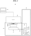
- FIG. 1 is an example of a schematic cross-sectional view illustrating a configuration of the inspection apparatus 10 according to the embodiment.
- the inspection apparatus 10 is configured to respectively inspect electrical characteristics of a plurality of electronic devices disposed on a wafer (inspection target) W.
- the inspection target is not limited to the wafer W, and includes a carrier, a glass substrate, a single chip, or the like having electronic devices thereon.
- the inspection apparatus 10 includes an accommodating chamber 12 accommodating a stage 11 on which the wafer W is placed, a loader 13 disposed adjacent to the accommodating chamber 12, and a tester 14 disposed to cover the accommodating chamber 12.
- the accommodation chamber 12 has a hollow housing shape.
- the stage 11 on which the wafer W is placed and a probe card 15 disposed to face the stage 11 are accommodated.
- the probe card 15 has a plurality of needle-shaped probes (contact terminals) 16 arranged to correspond to solder bumps or electrode pads installed correspondingly to electrodes of each electronic device of the wafer W.
- the stage 11 has a fixing mechanism (not shown) for fixing the wafer W to the stage 11. Accordingly, the displacement of the position of the wafer W with respect to the stage 11 is prevented. Further, a moving mechanism (not shown) for moving the stage 11 in a horizontal direction and a vertical direction is disposed in the accommodating chamber 12. Accordingly, the solder bumps or the electrodes pads installed correspondingly to electrodes of each electronic device are brought into contact with the probes 16 of the probe card 15 by adjusting a relative position between the probe card 15 and the wafer W.
- the loader 13 is configured to extract a wafer W having the electronic devices thereon from a FOUP (not shown) that is a transfer container and places the wafer W on the stage 11 in the accommodating chamber 12. Further, the loader 13 is configured to remove an inspected wafer W from the stage 11 and accommodates the inspected wafer W in the FOUP.
- the probe card 15 is connected to the tester 14 through an interface 17.
- the probes 16 When the probes 16 are brought into contact with the solder bumps or the electrode pads installed correspondingly to the electrodes of each electronic device of the wafer W, the probes 16 supply electric power from the tester 14 to the electronic device through the interface 17 or transmits signals from the electronic device to the tester 14 through the interface 17.
- the tester 14 includes a test board (not shown) that emulates a part of a circuit configuration of a motherboard on which the electronic devices are installed.
- the test board is connected to a tester computer 18 that is configured to determine whether the electronic devices are defective or non-defective based on the signals from the electronic devices.
- the tester 14 it is possible to emulate the circuit configurations of various types of motherboards by replacing the test board.
- a controller 19 controls an operation of the stage 11.
- the controller 19 controls the moving mechanism (not shown) of the stage 11 to move the stage 11 in the horizontal direction and the vertical direction. Further, the controller 19 is connected to a light irradiator 20 through a wiring 23.
- the controller 19 controls an operation of the light irradiator 20 through the wiring 23, which will be described later.
- a coolant supply device 31 is connected to a coolant channel 30 of the stage 11 through a supply pipe 32 and a return pipe 33, and the coolant can be circulated between the coolant supply device 31 and the coolant channel 30 of the stage 11.
- the controller 19 controls the coolant supply device 31 to control a temperature, a flow rate, or the like of the coolant that is supplied from the coolant supply device 31 to the coolant channel 30.
- controller 19 and the coolant supply device 31 are disposed in the loader 13, the present disclosure is not limited thereto and the controller 19 and the coolant supply device 31 may be disposed at other portions.
- the tester computer 18 transmits data to the test board connected through the electronic devices and the probes 16. Then, the tester computer 18 determines whether or not the transmitted data has been correctly processed by the test board based on the electrical signals from the test board.
- Fig. 2 is an example of a schematic cross-sectional view illustrating the temperature adjusting mechanism of the wafer W in the inspection apparatus 10 according to the embodiment.
- the wafer W on which electronic devices are formed is placed on the stage 11.
- the coolant channel (cooler) 30 is formed in the stage 11.
- the coolant is supplied from the coolant supply device 31 (see Fig. 1 ) to the coolant channel 30 through the supply pipe 32 (see Fig. 1 ) .
- the coolant flowing through the coolant channel 30 is returned to the coolant supply device 31 through the return pipe 33 (see Fig. 1 ) .
- the coolant may be, for example, Galden (Registered Trademark) or colorless liquid that allows light to pass therethrough such as water.
- the probe card 15 has a light irradiator 20 that irradiates light to heat the electronic devices of the wafer W from right above the upper surface of the wafer W (the upper surface being opposite to the bottom surface of the wafer W placed on the stage).
- the light irradiator 20 includes an LED array 21 and an LED control board 22.
- the LED control board 22 controls the on/off of the LED array 21. Further, the LED array 21 is supported by the LED control board 22 while being inclined toward the electronic devices (electronic devices under inspection) to which the probes 16 are connected. Further, the LED array 21 is provided with a lens (not shown) for controlling directivity of LED light so that the LED light can be irradiated to the electronic devices under inspection.
- the LED control board 22 supports the LED array 21 and is suspended from the probe card 15. The LED control board 22 is connected to the controller 19 (see Fig. 1 ) through the wiring 23 (see Fig. 1 ).
- Fig. 3 is an example of a schematic cross-sectional view illustrating the temperature adjustment of the wafer W in the inspection apparatus 10 according to the embodiment.
- the electronic devices When the electronic devices are inspected, electric power is supplied from the tester 14 to the electronic devices of the wafer W through the probes 16. Accordingly, the electronic devices of the wafer W generate heat. In Fig. 3 , such a region is illustrated as a heat generating region 40. Further, the controller 19 controls the light irradiator 20. In Fig. 3 , light 25 emitted from the light irradiator 20 is indicated by a double dotted line. The light emitted from the light irradiator 20 is irradiated to the heat generating region 40 from right above the upper surface of the wafer W. Further, the coolant is supplied to the coolant channel 30. Accordingly, the heat of the heat generating region 40 is absorbed by the coolant in the coolant channel 30 through the stage 11 as indicated by a white arrow.
- Fig. 4 is an example of a graph illustrating the amount of heat generated in the heat generating region 40 of the wafer W.
- the vertical axis represents a heat emission amount and the horizontal axis represents time.
- the controller 19 controls the time-varying changes of the light amount of the light irradiator 20 depending on the time-varying changes of the heat emission amount 101 of the electronic device itself. Specifically, a total device heat emission amount 102 that is the sum of a heat emission amount 111 of the electronic device itself due to the electric power supply and a heat emission amount 112 due to the light irradiator 20 is controlled to be constant.
- the electronic devices can be directly heated by irradiating the light from right above the the upper surface of the wafer W. Accordingly, the responsiveness of the temperature control of the electronic devices can be improved.
- the total heat emission amount can be maintained at a constant level by controlling the heating amount of the electronic devices by the light irradiator 20.
- the coolant channel 30 is controlled to absorb a constant amount of heat. Accordingly, the temperatures of the electronic devices can be maintained at a constant level during the inspection of the electronic devices.
- the degree of freedom in designing the coolant channel 30 in the stage 11 is improved. Accordingly, it is easy to assemble a high heat-absorbing cooler, such as a microchannel structure, a heat pipe structure, or the like.
- Fig. 5 is an example of a schematic view of the LED array 21 viewed from an irradiation surface side.
- the LED array 21 is disposed to surround the outer periphery of the probes 16 (see Fig. 2 ).
- the LED array 21 includes, e.g., an LED array group 251 that irradiates light to an outer peripheral side of an electronic device to be inspected, an LED array group 252 that irradiates light to an intermediate portion (between the outer peripheral portion and a central portion) of the electronic device to be inspected, and an LED array group 253 that illuminates light to the central portion (inner peripheral side) of the electronic device.
- the controller 19 can adjust the light amount distribution of the light irradiated to the wafer W by controlling the light amount of each LED depending on the arrangement position of the LEDs.
- the controller 19 can control the light amount for each of the LED array groups 251 to 253.
- the controller 19 is configured to control the light amount distribution of the light irradiator 20 that irradiates light to the electronic devices.
- Fig. 5 it is illustrated that the LED array 21 is arranged in three rows from the central portion toward the outer peripheral side.
- the present disclosure is not limited thereto.
- the arrangement of the LED array groups is not limited thereto.
- the electronic device When the electronic device is inspected, the electronic device generates heat due to an output supplied from the probes 16.
- heat of an outer peripheral portion of a chip of the electronic device is dissipated to its neighboring portions.
- a heat is stored in a central portion of the chip of the electronic device. Therefore, non-uniform heat distribution (temperature distribution) occurs in the electronic device.
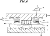
- Fig. 6 is an example of a schematic cross-sectional view illustrating the temperature adjustment of the wafer W in the inspection apparatus 10 according to the embodiment.
- the controller 19 controls light amount distribution 26 of the light irradiator 20 based on the heat distribution of the electronic device.
- Fig. 6 schematically shows the light amount distribution 26 of the light irradiator 20.
- the light amount of the LED array group 251 that irradiates light to the outer peripheral side of the electronic device is controlled to be stronger than the light amount of the LED array group 253 that irradiates light to the inner peripheral side of the electronic device. Accordingly, the heat distribution on the surface of the electronic device can become uniform.
- the inspected object of the inspection apparatus 10 has been described by taking a wafer W on which a plurality of electronic devices are formed as an example, but the present invention is not limited thereto.
- the object to be inspected by the inspection apparatus 10 may be a carrier C in which a plurality of electronic devices are arranged.
- the light source is not limited thereto, and may be a lamp or the like.
Landscapes
- Engineering & Computer Science (AREA)
- Physics & Mathematics (AREA)
- General Physics & Mathematics (AREA)
- General Engineering & Computer Science (AREA)
- Toxicology (AREA)
- Health & Medical Sciences (AREA)
- Environmental & Geological Engineering (AREA)
- Microelectronics & Electronic Packaging (AREA)
- Computer Hardware Design (AREA)
- Computer Vision & Pattern Recognition (AREA)
- Electromagnetism (AREA)
- Manufacturing & Machinery (AREA)
- Testing Or Measuring Of Semiconductors Or The Like (AREA)
- Testing Of Individual Semiconductor Devices (AREA)
Abstract
Description
- The present disclosure relates to an inspection apparatus.
- There is known an inspection apparatus in which a wafer or a carrier having electronic devices thereon is placed on a substrate support and electrical characteristics of the electronic devices are inspected by supplying a current from a tester to the electronic devices through probes or the like. Temperatures of the electronic devices are controlled by a cooler or a heater in the substrate support.
-
Japanese Patent Application Publication No. 2018-151369 - In
Japanese Patent Application Publication No. 2018-151369 - In view of the above, the present disclosure provides an inspection device that improves responsiveness of temperature control of a substrate.
- In accordance with an aspect of the present disclosure, there is provided an inspection apparatus including a stage on which a substrate is placed; a cooler to cool the substrate placed on the stage; a probe card having probes to be in contact with the substrate to supply electric power; a light irradiator to irradiate light to an upper surface of the substrate; and a controller to control the light irradiator.
- The objects and features of the present disclosure will become apparent from the following description of embodiments, given in conjunction with the accompanying drawings, in which:
-
Fig. 1 is an example of a schematic cross-sectional view illustrating a configuration of an inspection apparatus according to an embodiment; -
Fig. 2 is an example of a schematic cross-sectional view illustrating a wafer temperature control mechanism in the inspection apparatus according to the embodiment; -
Fig. 3 is an example of a schematic cross-sectional view illustrating temperature control of a wafer in the inspection apparatus according to the embodiment; -
Fig. 4 is an example of a graph illustrating the amount of heat generated in a heat generation region of the wafer; -
Fig. 5 is an example of a schematic view of an LED array viewed from an irradiation surface side; and. -
Fig. 6 is an example of a schematic cross-sectional view illustrating the temperature control of the wafer in the inspection apparatus according to the embodiment. - Hereinafter, embodiments will be described in detail with reference to the accompanying drawings. Like reference numerals will be given to like parts throughout the drawings, and redundant description thereof may be omitted.
- An
inspection apparatus 10 including a stage (substrate support) 11 according to an embodiment will be described with reference toFig. 1. Fig. 1 is an example of a schematic cross-sectional view illustrating a configuration of theinspection apparatus 10 according to the embodiment. - The
inspection apparatus 10 is configured to respectively inspect electrical characteristics of a plurality of electronic devices disposed on a wafer (inspection target) W. The inspection target is not limited to the wafer W, and includes a carrier, a glass substrate, a single chip, or the like having electronic devices thereon. Theinspection apparatus 10 includes anaccommodating chamber 12 accommodating astage 11 on which the wafer W is placed, aloader 13 disposed adjacent to theaccommodating chamber 12, and atester 14 disposed to cover theaccommodating chamber 12. - The
accommodation chamber 12 has a hollow housing shape. In theaccommodating chamber 12, thestage 11 on which the wafer W is placed and aprobe card 15 disposed to face thestage 11 are accommodated. Theprobe card 15 has a plurality of needle-shaped probes (contact terminals) 16 arranged to correspond to solder bumps or electrode pads installed correspondingly to electrodes of each electronic device of the wafer W. - The
stage 11 has a fixing mechanism (not shown) for fixing the wafer W to thestage 11. Accordingly, the displacement of the position of the wafer W with respect to thestage 11 is prevented. Further, a moving mechanism (not shown) for moving thestage 11 in a horizontal direction and a vertical direction is disposed in theaccommodating chamber 12. Accordingly, the solder bumps or the electrodes pads installed correspondingly to electrodes of each electronic device are brought into contact with theprobes 16 of theprobe card 15 by adjusting a relative position between theprobe card 15 and the wafer W. - The
loader 13 is configured to extract a wafer W having the electronic devices thereon from a FOUP (not shown) that is a transfer container and places the wafer W on thestage 11 in theaccommodating chamber 12. Further, theloader 13 is configured to remove an inspected wafer W from thestage 11 and accommodates the inspected wafer W in the FOUP. - The
probe card 15 is connected to thetester 14 through aninterface 17. When theprobes 16 are brought into contact with the solder bumps or the electrode pads installed correspondingly to the electrodes of each electronic device of the wafer W, theprobes 16 supply electric power from thetester 14 to the electronic device through theinterface 17 or transmits signals from the electronic device to thetester 14 through theinterface 17. - The
tester 14 includes a test board (not shown) that emulates a part of a circuit configuration of a motherboard on which the electronic devices are installed. The test board is connected to atester computer 18 that is configured to determine whether the electronic devices are defective or non-defective based on the signals from the electronic devices. In thetester 14, it is possible to emulate the circuit configurations of various types of motherboards by replacing the test board. - A
controller 19 controls an operation of thestage 11. Thecontroller 19 controls the moving mechanism (not shown) of thestage 11 to move thestage 11 in the horizontal direction and the vertical direction. Further, thecontroller 19 is connected to alight irradiator 20 through awiring 23. Thecontroller 19 controls an operation of thelight irradiator 20 through thewiring 23, which will be described later. - A
coolant supply device 31 is connected to acoolant channel 30 of thestage 11 through asupply pipe 32 and areturn pipe 33, and the coolant can be circulated between thecoolant supply device 31 and thecoolant channel 30 of thestage 11. Thecontroller 19 controls thecoolant supply device 31 to control a temperature, a flow rate, or the like of the coolant that is supplied from thecoolant supply device 31 to thecoolant channel 30. - Although it is illustrated in
Fig. 1 that thecontroller 19 and thecoolant supply device 31 are disposed in theloader 13, the present disclosure is not limited thereto and thecontroller 19 and thecoolant supply device 31 may be disposed at other portions. - In the
inspection apparatus 10, when the electrical characteristics of the electronic devices are inspected, thetester computer 18 transmits data to the test board connected through the electronic devices and theprobes 16. Then, thetester computer 18 determines whether or not the transmitted data has been correctly processed by the test board based on the electrical signals from the test board. - Next, a temperature control mechanism of the wafer W in the
inspection apparatus 10 according to the embodiment will be described with reference toFig. 2. Fig. 2 is an example of a schematic cross-sectional view illustrating the temperature adjusting mechanism of the wafer W in theinspection apparatus 10 according to the embodiment. - The wafer W on which electronic devices are formed is placed on the
stage 11. The coolant channel (cooler) 30 is formed in thestage 11. The coolant is supplied from the coolant supply device 31 (seeFig. 1 ) to thecoolant channel 30 through the supply pipe 32 (seeFig. 1 ) . The coolant flowing through thecoolant channel 30 is returned to thecoolant supply device 31 through the return pipe 33 (seeFig. 1 ) . The coolant may be, for example, Galden (Registered Trademark) or colorless liquid that allows light to pass therethrough such as water. - The
probe card 15 has alight irradiator 20 that irradiates light to heat the electronic devices of the wafer W from right above the upper surface of the wafer W (the upper surface being opposite to the bottom surface of the wafer W placed on the stage). Thelight irradiator 20 includes anLED array 21 and anLED control board 22. TheLED control board 22 controls the on/off of theLED array 21. Further, theLED array 21 is supported by theLED control board 22 while being inclined toward the electronic devices (electronic devices under inspection) to which theprobes 16 are connected. Further, theLED array 21 is provided with a lens (not shown) for controlling directivity of LED light so that the LED light can be irradiated to the electronic devices under inspection. TheLED control board 22 supports theLED array 21 and is suspended from theprobe card 15. TheLED control board 22 is connected to the controller 19 (seeFig. 1 ) through the wiring 23 (seeFig. 1 ). -
Fig. 3 is an example of a schematic cross-sectional view illustrating the temperature adjustment of the wafer W in theinspection apparatus 10 according to the embodiment. - When the electronic devices are inspected, electric power is supplied from the
tester 14 to the electronic devices of the wafer W through theprobes 16. Accordingly, the electronic devices of the wafer W generate heat. InFig. 3 , such a region is illustrated as aheat generating region 40. Further, thecontroller 19 controls thelight irradiator 20. InFig. 3 , light 25 emitted from thelight irradiator 20 is indicated by a double dotted line. The light emitted from thelight irradiator 20 is irradiated to theheat generating region 40 from right above the upper surface of the wafer W. Further, the coolant is supplied to thecoolant channel 30. Accordingly, the heat of theheat generating region 40 is absorbed by the coolant in thecoolant channel 30 through thestage 11 as indicated by a white arrow. -
Fig. 4 is an example of a graph illustrating the amount of heat generated in theheat generating region 40 of the wafer W. InFig. 4 , the vertical axis represents a heat emission amount and the horizontal axis represents time. When the electronic devices are inspected, the electric power supplied from theprobes 16 to the electronic devices of the wafer W changes depending on the inspection content. Therefore, aheat emission amount 101 of the electronic device itself changes with time. - The
controller 19 controls the time-varying changes of the light amount of thelight irradiator 20 depending on the time-varying changes of theheat emission amount 101 of the electronic device itself. Specifically, a total deviceheat emission amount 102 that is the sum of aheat emission amount 111 of the electronic device itself due to the electric power supply and aheat emission amount 112 due to thelight irradiator 20 is controlled to be constant. - In the
inspection apparatus 10 of the present embodiment, the electronic devices can be directly heated by irradiating the light from right above the the upper surface of the wafer W. Accordingly, the responsiveness of the temperature control of the electronic devices can be improved. - Further, in the
inspection apparatus 10 of the present embodiment, even when the heat emission amount of the electronic devices changes due to the change in the electric power supply during the inspection of the electronic devices, the total heat emission amount can be maintained at a constant level by controlling the heating amount of the electronic devices by thelight irradiator 20. At this time, thecoolant channel 30 is controlled to absorb a constant amount of heat. Accordingly, the temperatures of the electronic devices can be maintained at a constant level during the inspection of the electronic devices. - Further, due to the configuration in which the
light irradiator 20 irradiates light from right above the upper surface of the wafer W, the degree of freedom in designing thecoolant channel 30 in thestage 11 is improved. Accordingly, it is easy to assemble a high heat-absorbing cooler, such as a microchannel structure, a heat pipe structure, or the like. -
Fig. 5 is an example of a schematic view of theLED array 21 viewed from an irradiation surface side. TheLED array 21 is disposed to surround the outer periphery of the probes 16 (seeFig. 2 ). TheLED array 21 includes, e.g., anLED array group 251 that irradiates light to an outer peripheral side of an electronic device to be inspected, anLED array group 252 that irradiates light to an intermediate portion (between the outer peripheral portion and a central portion) of the electronic device to be inspected, and anLED array group 253 that illuminates light to the central portion (inner peripheral side) of the electronic device. Thecontroller 19 can adjust the light amount distribution of the light irradiated to the wafer W by controlling the light amount of each LED depending on the arrangement position of the LEDs. For example, thecontroller 19 can control the light amount for each of theLED array groups 251 to 253. In other words, thecontroller 19 is configured to control the light amount distribution of thelight irradiator 20 that irradiates light to the electronic devices. InFig. 5 , it is illustrated that theLED array 21 is arranged in three rows from the central portion toward the outer peripheral side. However, the present disclosure is not limited thereto. Further, although the case where the light amount is controlled for each of the three LED array groups has been described, the arrangement of the LED array groups is not limited thereto. - When the electronic device is inspected, the electronic device generates heat due to an output supplied from the
probes 16. In this specification, heat of an outer peripheral portion of a chip of the electronic device is dissipated to its neighboring portions. On the other hand, a heat is stored in a central portion of the chip of the electronic device. Therefore, non-uniform heat distribution (temperature distribution) occurs in the electronic device. -
Fig. 6 is an example of a schematic cross-sectional view illustrating the temperature adjustment of the wafer W in theinspection apparatus 10 according to the embodiment. - The
controller 19 controlslight amount distribution 26 of thelight irradiator 20 based on the heat distribution of the electronic device.Fig. 6 schematically shows thelight amount distribution 26 of thelight irradiator 20. For example, the light amount of theLED array group 251 that irradiates light to the outer peripheral side of the electronic device is controlled to be stronger than the light amount of theLED array group 253 that irradiates light to the inner peripheral side of the electronic device. Accordingly, the heat distribution on the surface of the electronic device can become uniform. - While the
inspection apparatus 10 has been described above, the present disclosure is not limited to the above-described embodiments, and various changes and modifications can be made without departing from the scope of the appended claims and the gist thereof. - The inspected object of the
inspection apparatus 10 has been described by taking a wafer W on which a plurality of electronic devices are formed as an example, but the present invention is not limited thereto. The object to be inspected by theinspection apparatus 10 may be a carrier C in which a plurality of electronic devices are arranged. - Although the
light irradiator 20 using the LEDs as a light source has been described, the light source is not limited thereto, and may be a lamp or the like. - While certain embodiments have been described, these embodiments have been presented by way of example only, and are not intended to limit the scope of the disclosures. Indeed, the embodiments described herein may be embodied in a variety of other forms. Furthermore, various omissions, substitutions and changes to the embodiments described herein may be made without departing from the spirit of the disclosures. The accompanying claims and their equivalents are intended to cover such forms or modifications as would fall within the scope and spirit of the disclosures.
Claims (9)
- An inspection apparatus comprising:a stage on which a substrate is placed;a cooler to cool the substrate placed on the stage;a probe card having probes to be in contact with the substrate to supply electric power;a light irradiator to irradiate light to an upper surface of the substrate, opposite to a bottom surface of the substrate placed on the stage; anda controller to control the light irradiator.
- The inspection apparatus of claim 1, wherein the controller controls the light amount of the light irradiator based on a heat emission amount of the substrate due to the electric power supply.
- The inspection apparatus of claim 2, wherein the controller controls time-varing changes of the light amount of the light irradiator based on time-varying changes of the heat emission amount of the substrate due to the electric power supply.
- The inspection apparatus of claim 3, wherein the controller controls the light amount of the light irradiator or the time-vayring changes of the light amount of the light irradiation amount based on the sum of the heat emission amount of the substrate due to the electric power supply and the heat emission amount of the substrate due to the light irradiated by the light irradiator.
- The inspection apparatus of any one of claims 1 to 4, wherein the controller controls light amount distribution of the light irradiator based on heat distribution of the substrate.
- The inspection apparatus of claim 5, wherein the substrate has a device to which the electric power from the probes is supplied, and
the controller controls the light amount distribution of the light irradiator such that the amount of light irradiated to an outer peripheral portion of the device becomes greater than the amount of light irradiated to an inner peripheral portion of the device. - The inspection apparatus of any one of claims 1 to 6, wherein the light irradiator includes multiple light sources, and
the light sources are arranged at outer peripheries of the probes. - The inspection apparatus of claim 7, wherein the controller controls the light amount of each of the light sources depending on the arrangement positions of the light sources, and controls the light amount distribution of the light irradiator.
- The inspection apparatus of claim 8, wherein the light sources are arranged in multiple rows in a radial direction at the outer peripheries of the probes, and
the controller controls the light amount of each of the light sources by dividing the light sources arranged in the multiple rows into an inner peripheral side light source group and an outer peripheral side light source group, and controls the light amount distribution of the light irradiator.
Applications Claiming Priority (1)
| Application Number | Priority Date | Filing Date | Title |
|---|---|---|---|
| JP2020120860A JP7455015B2 (en) | 2020-07-14 | 2020-07-14 | Inspection equipment |
Publications (2)
| Publication Number | Publication Date |
|---|---|
| EP3940402A1 true EP3940402A1 (en) | 2022-01-19 |
| EP3940402B1 EP3940402B1 (en) | 2023-09-27 |
Family
ID=76920678
Family Applications (1)
| Application Number | Title | Priority Date | Filing Date |
|---|---|---|---|
| EP21185534.1A Active EP3940402B1 (en) | 2020-07-14 | 2021-07-14 | Inspection apparatus |
Country Status (6)
| Country | Link |
|---|---|
| US (1) | US11536768B2 (en) |
| EP (1) | EP3940402B1 (en) |
| JP (1) | JP7455015B2 (en) |
| KR (1) | KR102665977B1 (en) |
| CN (1) | CN113937021B (en) |
| TW (1) | TWI905221B (en) |
Families Citing this family (1)
| Publication number | Priority date | Publication date | Assignee | Title |
|---|---|---|---|---|
| KR102808414B1 (en) | 2022-11-18 | 2025-05-16 | 삼성전자주식회사 | Probe Card |
Citations (3)
| Publication number | Priority date | Publication date | Assignee | Title |
|---|---|---|---|---|
| US6078183A (en) * | 1998-03-03 | 2000-06-20 | Sandia Corporation | Thermally-induced voltage alteration for integrated circuit analysis |
| US20050287685A1 (en) * | 2004-06-14 | 2005-12-29 | Mcfadden Bruce | Localizing a temperature of a device for testing |
| JP2018151369A (en) | 2016-11-29 | 2018-09-27 | 東京エレクトロン株式会社 | Placing stand and electronic device inspection apparatus |
Family Cites Families (13)
| Publication number | Priority date | Publication date | Assignee | Title |
|---|---|---|---|---|
| JPS5068069A (en) * | 1973-10-17 | 1975-06-07 | ||
| JPH0494733U (en) * | 1991-01-17 | 1992-08-17 | ||
| JPH0722477A (en) * | 1993-06-29 | 1995-01-24 | Nec Yamaguchi Ltd | Semiconductor integrated circuit measuring device |
| JP2002055146A (en) | 2000-08-10 | 2002-02-20 | Hitachi Ltd | Method for manufacturing semiconductor device |
| US7071714B2 (en) * | 2001-11-02 | 2006-07-04 | Formfactor, Inc. | Method and system for compensating for thermally induced motion of probe cards |
| JP2009170730A (en) * | 2008-01-17 | 2009-07-30 | Fujifilm Corp | Back-illuminated solid-state image sensor inspection device |
| JP5861557B2 (en) | 2012-04-26 | 2016-02-16 | 三菱電機株式会社 | Inspection device |
| CN105514008A (en) * | 2015-12-14 | 2016-04-20 | 重庆远创光电科技有限公司 | Chip carrying apparatus with light source |
| CN109983350B (en) * | 2016-11-29 | 2022-02-22 | 东京毅力科创株式会社 | Stages and test equipment for electronic devices |
| US11107708B2 (en) * | 2017-11-14 | 2021-08-31 | Taiwan Semiconductor Manufacturing Company, Ltd. | Heating platform, thermal treatment and manufacturing method |
| JP7078838B2 (en) | 2017-12-01 | 2022-06-01 | 東京エレクトロン株式会社 | Prober |
| JP7161854B2 (en) * | 2018-03-05 | 2022-10-27 | 東京エレクトロン株式会社 | inspection equipment |
| JP7042158B2 (en) * | 2018-05-23 | 2022-03-25 | 東京エレクトロン株式会社 | Inspection device and temperature control method |
-
2020
- 2020-07-14 JP JP2020120860A patent/JP7455015B2/en active Active
-
2021
- 2021-07-02 KR KR1020210087356A patent/KR102665977B1/en active Active
- 2021-07-02 CN CN202110751970.5A patent/CN113937021B/en active Active
- 2021-07-05 TW TW110124564A patent/TWI905221B/en active
- 2021-07-13 US US17/374,660 patent/US11536768B2/en active Active
- 2021-07-14 EP EP21185534.1A patent/EP3940402B1/en active Active
Patent Citations (3)
| Publication number | Priority date | Publication date | Assignee | Title |
|---|---|---|---|---|
| US6078183A (en) * | 1998-03-03 | 2000-06-20 | Sandia Corporation | Thermally-induced voltage alteration for integrated circuit analysis |
| US20050287685A1 (en) * | 2004-06-14 | 2005-12-29 | Mcfadden Bruce | Localizing a temperature of a device for testing |
| JP2018151369A (en) | 2016-11-29 | 2018-09-27 | 東京エレクトロン株式会社 | Placing stand and electronic device inspection apparatus |
Also Published As
| Publication number | Publication date |
|---|---|
| CN113937021B (en) | 2025-12-05 |
| US11536768B2 (en) | 2022-12-27 |
| KR20220008765A (en) | 2022-01-21 |
| TWI905221B (en) | 2025-11-21 |
| JP7455015B2 (en) | 2024-03-25 |
| CN113937021A (en) | 2022-01-14 |
| US20220018898A1 (en) | 2022-01-20 |
| TW202209524A (en) | 2022-03-01 |
| EP3940402B1 (en) | 2023-09-27 |
| KR102665977B1 (en) | 2024-05-13 |
| JP2022017971A (en) | 2022-01-26 |
Similar Documents
| Publication | Publication Date | Title |
|---|---|---|
| JP7078838B2 (en) | Prober | |
| KR102387504B1 (en) | inspection device | |
| US20210382105A1 (en) | Inspection apparatus and inspection method | |
| US11536768B2 (en) | Inspection apparatus | |
| KR102753001B1 (en) | Control method of inspection apparatus and inspection apparatus | |
| US12436188B2 (en) | LED chuck | |
| US11874319B2 (en) | Inspection apparatus and control method for inspection apparatus | |
| JP7636103B2 (en) | Mounting table and inspection device | |
| KR102956151B1 (en) | Inspection apparatus and control method for inspection apparatus | |
| CN114258164B (en) | Control method of inspection device and inspection device |
Legal Events
| Date | Code | Title | Description |
|---|---|---|---|
| PUAI | Public reference made under article 153(3) epc to a published international application that has entered the european phase |
Free format text: ORIGINAL CODE: 0009012 |
|
| STAA | Information on the status of an ep patent application or granted ep patent |
Free format text: STATUS: REQUEST FOR EXAMINATION WAS MADE |
|
| 17P | Request for examination filed |
Effective date: 20210714 |
|
| AK | Designated contracting states |
Kind code of ref document: A1 Designated state(s): AL AT BE BG CH CY CZ DE DK EE ES FI FR GB GR HR HU IE IS IT LI LT LU LV MC MK MT NL NO PL PT RO RS SE SI SK SM TR |
|
| GRAP | Despatch of communication of intention to grant a patent |
Free format text: ORIGINAL CODE: EPIDOSNIGR1 |
|
| STAA | Information on the status of an ep patent application or granted ep patent |
Free format text: STATUS: GRANT OF PATENT IS INTENDED |
|
| RIC1 | Information provided on ipc code assigned before grant |
Ipc: G01R 31/308 20060101ALI20230331BHEP Ipc: G01R 31/28 20060101AFI20230331BHEP |
|
| INTG | Intention to grant announced |
Effective date: 20230425 |
|
| RAP3 | Party data changed (applicant data changed or rights of an application transferred) |
Owner name: TOKYO ELECTRON LIMITED |
|
| GRAS | Grant fee paid |
Free format text: ORIGINAL CODE: EPIDOSNIGR3 |
|
| GRAA | (expected) grant |
Free format text: ORIGINAL CODE: 0009210 |
|
| STAA | Information on the status of an ep patent application or granted ep patent |
Free format text: STATUS: THE PATENT HAS BEEN GRANTED |
|
| AK | Designated contracting states |
Kind code of ref document: B1 Designated state(s): AL AT BE BG CH CY CZ DE DK EE ES FI FR GB GR HR HU IE IS IT LI LT LU LV MC MK MT NL NO PL PT RO RS SE SI SK SM TR |
|
| REG | Reference to a national code |
Ref country code: GB Ref legal event code: FG4D |
|
| REG | Reference to a national code |
Ref country code: CH Ref legal event code: EP |
|
| REG | Reference to a national code |
Ref country code: DE Ref legal event code: R096 Ref document number: 602021005396 Country of ref document: DE |
|
| REG | Reference to a national code |
Ref country code: IE Ref legal event code: FG4D |
|
| REG | Reference to a national code |
Ref country code: LT Ref legal event code: MG9D |
|
| PG25 | Lapsed in a contracting state [announced via postgrant information from national office to epo] |
Ref country code: GR Free format text: LAPSE BECAUSE OF FAILURE TO SUBMIT A TRANSLATION OF THE DESCRIPTION OR TO PAY THE FEE WITHIN THE PRESCRIBED TIME-LIMIT Effective date: 20231228 |
|
| PG25 | Lapsed in a contracting state [announced via postgrant information from national office to epo] |
Ref country code: SE Free format text: LAPSE BECAUSE OF FAILURE TO SUBMIT A TRANSLATION OF THE DESCRIPTION OR TO PAY THE FEE WITHIN THE PRESCRIBED TIME-LIMIT Effective date: 20230927 Ref country code: RS Free format text: LAPSE BECAUSE OF FAILURE TO SUBMIT A TRANSLATION OF THE DESCRIPTION OR TO PAY THE FEE WITHIN THE PRESCRIBED TIME-LIMIT Effective date: 20230927 Ref country code: NO Free format text: LAPSE BECAUSE OF FAILURE TO SUBMIT A TRANSLATION OF THE DESCRIPTION OR TO PAY THE FEE WITHIN THE PRESCRIBED TIME-LIMIT Effective date: 20231227 Ref country code: LV Free format text: LAPSE BECAUSE OF FAILURE TO SUBMIT A TRANSLATION OF THE DESCRIPTION OR TO PAY THE FEE WITHIN THE PRESCRIBED TIME-LIMIT Effective date: 20230927 Ref country code: LT Free format text: LAPSE BECAUSE OF FAILURE TO SUBMIT A TRANSLATION OF THE DESCRIPTION OR TO PAY THE FEE WITHIN THE PRESCRIBED TIME-LIMIT Effective date: 20230927 Ref country code: HR Free format text: LAPSE BECAUSE OF FAILURE TO SUBMIT A TRANSLATION OF THE DESCRIPTION OR TO PAY THE FEE WITHIN THE PRESCRIBED TIME-LIMIT Effective date: 20230927 Ref country code: GR Free format text: LAPSE BECAUSE OF FAILURE TO SUBMIT A TRANSLATION OF THE DESCRIPTION OR TO PAY THE FEE WITHIN THE PRESCRIBED TIME-LIMIT Effective date: 20231228 Ref country code: FI Free format text: LAPSE BECAUSE OF FAILURE TO SUBMIT A TRANSLATION OF THE DESCRIPTION OR TO PAY THE FEE WITHIN THE PRESCRIBED TIME-LIMIT Effective date: 20230927 |
|
| REG | Reference to a national code |
Ref country code: NL Ref legal event code: MP Effective date: 20230927 |
|
| REG | Reference to a national code |
Ref country code: AT Ref legal event code: MK05 Ref document number: 1615918 Country of ref document: AT Kind code of ref document: T Effective date: 20230927 |
|
| PG25 | Lapsed in a contracting state [announced via postgrant information from national office to epo] |
Ref country code: NL Free format text: LAPSE BECAUSE OF FAILURE TO SUBMIT A TRANSLATION OF THE DESCRIPTION OR TO PAY THE FEE WITHIN THE PRESCRIBED TIME-LIMIT Effective date: 20230927 |
|
| PG25 | Lapsed in a contracting state [announced via postgrant information from national office to epo] |
Ref country code: IS Free format text: LAPSE BECAUSE OF FAILURE TO SUBMIT A TRANSLATION OF THE DESCRIPTION OR TO PAY THE FEE WITHIN THE PRESCRIBED TIME-LIMIT Effective date: 20240127 |
|
| PG25 | Lapsed in a contracting state [announced via postgrant information from national office to epo] |
Ref country code: AT Free format text: LAPSE BECAUSE OF FAILURE TO SUBMIT A TRANSLATION OF THE DESCRIPTION OR TO PAY THE FEE WITHIN THE PRESCRIBED TIME-LIMIT Effective date: 20230927 |
|
| PG25 | Lapsed in a contracting state [announced via postgrant information from national office to epo] |
Ref country code: ES Free format text: LAPSE BECAUSE OF FAILURE TO SUBMIT A TRANSLATION OF THE DESCRIPTION OR TO PAY THE FEE WITHIN THE PRESCRIBED TIME-LIMIT Effective date: 20230927 |
|
| PG25 | Lapsed in a contracting state [announced via postgrant information from national office to epo] |
Ref country code: SM Free format text: LAPSE BECAUSE OF FAILURE TO SUBMIT A TRANSLATION OF THE DESCRIPTION OR TO PAY THE FEE WITHIN THE PRESCRIBED TIME-LIMIT Effective date: 20230927 Ref country code: RO Free format text: LAPSE BECAUSE OF FAILURE TO SUBMIT A TRANSLATION OF THE DESCRIPTION OR TO PAY THE FEE WITHIN THE PRESCRIBED TIME-LIMIT Effective date: 20230927 Ref country code: IS Free format text: LAPSE BECAUSE OF FAILURE TO SUBMIT A TRANSLATION OF THE DESCRIPTION OR TO PAY THE FEE WITHIN THE PRESCRIBED TIME-LIMIT Effective date: 20240127 Ref country code: ES Free format text: LAPSE BECAUSE OF FAILURE TO SUBMIT A TRANSLATION OF THE DESCRIPTION OR TO PAY THE FEE WITHIN THE PRESCRIBED TIME-LIMIT Effective date: 20230927 Ref country code: EE Free format text: LAPSE BECAUSE OF FAILURE TO SUBMIT A TRANSLATION OF THE DESCRIPTION OR TO PAY THE FEE WITHIN THE PRESCRIBED TIME-LIMIT Effective date: 20230927 Ref country code: CZ Free format text: LAPSE BECAUSE OF FAILURE TO SUBMIT A TRANSLATION OF THE DESCRIPTION OR TO PAY THE FEE WITHIN THE PRESCRIBED TIME-LIMIT Effective date: 20230927 Ref country code: AT Free format text: LAPSE BECAUSE OF FAILURE TO SUBMIT A TRANSLATION OF THE DESCRIPTION OR TO PAY THE FEE WITHIN THE PRESCRIBED TIME-LIMIT Effective date: 20230927 Ref country code: SK Free format text: LAPSE BECAUSE OF FAILURE TO SUBMIT A TRANSLATION OF THE DESCRIPTION OR TO PAY THE FEE WITHIN THE PRESCRIBED TIME-LIMIT Effective date: 20230927 Ref country code: PT Free format text: LAPSE BECAUSE OF FAILURE TO SUBMIT A TRANSLATION OF THE DESCRIPTION OR TO PAY THE FEE WITHIN THE PRESCRIBED TIME-LIMIT Effective date: 20240129 |
|
| PG25 | Lapsed in a contracting state [announced via postgrant information from national office to epo] |
Ref country code: PL Free format text: LAPSE BECAUSE OF FAILURE TO SUBMIT A TRANSLATION OF THE DESCRIPTION OR TO PAY THE FEE WITHIN THE PRESCRIBED TIME-LIMIT Effective date: 20230927 Ref country code: IT Free format text: LAPSE BECAUSE OF FAILURE TO SUBMIT A TRANSLATION OF THE DESCRIPTION OR TO PAY THE FEE WITHIN THE PRESCRIBED TIME-LIMIT Effective date: 20230927 |
|
| REG | Reference to a national code |
Ref country code: DE Ref legal event code: R097 Ref document number: 602021005396 Country of ref document: DE |
|
| PG25 | Lapsed in a contracting state [announced via postgrant information from national office to epo] |
Ref country code: DK Free format text: LAPSE BECAUSE OF FAILURE TO SUBMIT A TRANSLATION OF THE DESCRIPTION OR TO PAY THE FEE WITHIN THE PRESCRIBED TIME-LIMIT Effective date: 20230927 |
|
| PG25 | Lapsed in a contracting state [announced via postgrant information from national office to epo] |
Ref country code: DK Free format text: LAPSE BECAUSE OF FAILURE TO SUBMIT A TRANSLATION OF THE DESCRIPTION OR TO PAY THE FEE WITHIN THE PRESCRIBED TIME-LIMIT Effective date: 20230927 |
|
| PLBE | No opposition filed within time limit |
Free format text: ORIGINAL CODE: 0009261 |
|
| STAA | Information on the status of an ep patent application or granted ep patent |
Free format text: STATUS: NO OPPOSITION FILED WITHIN TIME LIMIT |
|
| 26N | No opposition filed |
Effective date: 20240628 |
|
| PG25 | Lapsed in a contracting state [announced via postgrant information from national office to epo] |
Ref country code: SI Free format text: LAPSE BECAUSE OF FAILURE TO SUBMIT A TRANSLATION OF THE DESCRIPTION OR TO PAY THE FEE WITHIN THE PRESCRIBED TIME-LIMIT Effective date: 20230927 |
|
| PG25 | Lapsed in a contracting state [announced via postgrant information from national office to epo] |
Ref country code: SI Free format text: LAPSE BECAUSE OF FAILURE TO SUBMIT A TRANSLATION OF THE DESCRIPTION OR TO PAY THE FEE WITHIN THE PRESCRIBED TIME-LIMIT Effective date: 20230927 |
|
| PG25 | Lapsed in a contracting state [announced via postgrant information from national office to epo] |
Ref country code: BG Free format text: LAPSE BECAUSE OF FAILURE TO SUBMIT A TRANSLATION OF THE DESCRIPTION OR TO PAY THE FEE WITHIN THE PRESCRIBED TIME-LIMIT Effective date: 20230927 |
|
| PG25 | Lapsed in a contracting state [announced via postgrant information from national office to epo] |
Ref country code: BG Free format text: LAPSE BECAUSE OF FAILURE TO SUBMIT A TRANSLATION OF THE DESCRIPTION OR TO PAY THE FEE WITHIN THE PRESCRIBED TIME-LIMIT Effective date: 20230927 |
|
| PG25 | Lapsed in a contracting state [announced via postgrant information from national office to epo] |
Ref country code: MC Free format text: LAPSE BECAUSE OF FAILURE TO SUBMIT A TRANSLATION OF THE DESCRIPTION OR TO PAY THE FEE WITHIN THE PRESCRIBED TIME-LIMIT Effective date: 20230927 |
|
| REG | Reference to a national code |
Ref country code: CH Ref legal event code: PL |
|
| PG25 | Lapsed in a contracting state [announced via postgrant information from national office to epo] |
Ref country code: LU Free format text: LAPSE BECAUSE OF NON-PAYMENT OF DUE FEES Effective date: 20240714 |
|
| PG25 | Lapsed in a contracting state [announced via postgrant information from national office to epo] |
Ref country code: LU Free format text: LAPSE BECAUSE OF NON-PAYMENT OF DUE FEES Effective date: 20240714 |
|
| PG25 | Lapsed in a contracting state [announced via postgrant information from national office to epo] |
Ref country code: CH Free format text: LAPSE BECAUSE OF NON-PAYMENT OF DUE FEES Effective date: 20240731 Ref country code: BE Free format text: LAPSE BECAUSE OF NON-PAYMENT OF DUE FEES Effective date: 20240731 |
|
| PG25 | Lapsed in a contracting state [announced via postgrant information from national office to epo] |
Ref country code: FR Free format text: LAPSE BECAUSE OF NON-PAYMENT OF DUE FEES Effective date: 20240731 |
|
| REG | Reference to a national code |
Ref country code: BE Ref legal event code: MM Effective date: 20240731 |
|
| PG25 | Lapsed in a contracting state [announced via postgrant information from national office to epo] |
Ref country code: IE Free format text: LAPSE BECAUSE OF NON-PAYMENT OF DUE FEES Effective date: 20240714 |
|
| PGFP | Annual fee paid to national office [announced via postgrant information from national office to epo] |
Ref country code: DE Payment date: 20250528 Year of fee payment: 5 |
|
| PG25 | Lapsed in a contracting state [announced via postgrant information from national office to epo] |
Ref country code: CY Free format text: LAPSE BECAUSE OF FAILURE TO SUBMIT A TRANSLATION OF THE DESCRIPTION OR TO PAY THE FEE WITHIN THE PRESCRIBED TIME-LIMIT; INVALID AB INITIO Effective date: 20210714 |
|
| PG25 | Lapsed in a contracting state [announced via postgrant information from national office to epo] |
Ref country code: HU Free format text: LAPSE BECAUSE OF FAILURE TO SUBMIT A TRANSLATION OF THE DESCRIPTION OR TO PAY THE FEE WITHIN THE PRESCRIBED TIME-LIMIT; INVALID AB INITIO Effective date: 20210714 |
|
| GBPC | Gb: european patent ceased through non-payment of renewal fee |
Effective date: 20250714 |
|
| PG25 | Lapsed in a contracting state [announced via postgrant information from national office to epo] |
Ref country code: GB Free format text: LAPSE BECAUSE OF NON-PAYMENT OF DUE FEES Effective date: 20250714 |