EP3940337A1 - A method and apparatus for measuring a lateral depth in a microstructure - Google Patents
A method and apparatus for measuring a lateral depth in a microstructure Download PDFInfo
- Publication number
- EP3940337A1 EP3940337A1 EP21183291.0A EP21183291A EP3940337A1 EP 3940337 A1 EP3940337 A1 EP 3940337A1 EP 21183291 A EP21183291 A EP 21183291A EP 3940337 A1 EP3940337 A1 EP 3940337A1
- Authority
- EP
- European Patent Office
- Prior art keywords
- depth
- substrate
- response
- relation
- recess
- Prior art date
- Legal status (The legal status is an assumption and is not a legal conclusion. Google has not performed a legal analysis and makes no representation as to the accuracy of the status listed.)
- Granted
Links
Images


Classifications
-
- G—PHYSICS
- G01—MEASURING; TESTING
- G01B—MEASURING LENGTH, THICKNESS OR SIMILAR LINEAR DIMENSIONS; MEASURING ANGLES; MEASURING AREAS; MEASURING IRREGULARITIES OF SURFACES OR CONTOURS
- G01B11/00—Measuring arrangements characterised by the use of optical techniques
- G01B11/22—Measuring arrangements characterised by the use of optical techniques for measuring depth
-
- G—PHYSICS
- G01—MEASURING; TESTING
- G01N—INVESTIGATING OR ANALYSING MATERIALS BY DETERMINING THEIR CHEMICAL OR PHYSICAL PROPERTIES
- G01N21/00—Investigating or analysing materials by the use of optical means, i.e. using sub-millimetre waves, infrared, visible or ultraviolet light
- G01N21/62—Systems in which the material investigated is excited whereby it emits light or causes a change in wavelength of the incident light
- G01N21/63—Systems in which the material investigated is excited whereby it emits light or causes a change in wavelength of the incident light optically excited
- G01N21/65—Raman scattering
-
- G—PHYSICS
- G01—MEASURING; TESTING
- G01B—MEASURING LENGTH, THICKNESS OR SIMILAR LINEAR DIMENSIONS; MEASURING ANGLES; MEASURING AREAS; MEASURING IRREGULARITIES OF SURFACES OR CONTOURS
- G01B15/00—Measuring arrangements characterised by the use of electromagnetic waves or particle radiation, e.g. by the use of microwaves, X-rays, gamma rays or electrons
-
- H—ELECTRICITY
- H10—SEMICONDUCTOR DEVICES; ELECTRIC SOLID-STATE DEVICES NOT OTHERWISE PROVIDED FOR
- H10D—INORGANIC ELECTRIC SEMICONDUCTOR DEVICES
- H10D62/00—Semiconductor bodies, or regions thereof, of devices having potential barriers
- H10D62/10—Shapes, relative sizes or dispositions of the regions of the semiconductor bodies; Shapes of the semiconductor bodies
- H10D62/117—Shapes of semiconductor bodies
- H10D62/118—Nanostructure semiconductor bodies
- H10D62/119—Nanowire, nanosheet or nanotube semiconductor bodies
- H10D62/121—Nanowire, nanosheet or nanotube semiconductor bodies oriented parallel to substrates
-
- H—ELECTRICITY
- H10—SEMICONDUCTOR DEVICES; ELECTRIC SOLID-STATE DEVICES NOT OTHERWISE PROVIDED FOR
- H10P—GENERIC PROCESSES OR APPARATUS FOR THE MANUFACTURE OR TREATMENT OF DEVICES COVERED BY CLASS H10
- H10P74/00—Testing or measuring during manufacture or treatment of wafers, substrates or devices
- H10P74/20—Testing or measuring during manufacture or treatment of wafers, substrates or devices characterised by the properties tested or measured, e.g. structural or electrical properties
- H10P74/203—Structural properties, e.g. testing or measuring thicknesses, line widths, warpage, bond strengths or physical defects
-
- H—ELECTRICITY
- H10—SEMICONDUCTOR DEVICES; ELECTRIC SOLID-STATE DEVICES NOT OTHERWISE PROVIDED FOR
- H10P—GENERIC PROCESSES OR APPARATUS FOR THE MANUFACTURE OR TREATMENT OF DEVICES COVERED BY CLASS H10
- H10P74/00—Testing or measuring during manufacture or treatment of wafers, substrates or devices
- H10P74/23—Testing or measuring during manufacture or treatment of wafers, substrates or devices characterised by multiple measurements, corrections, marking or sorting processes
-
- H—ELECTRICITY
- H10—SEMICONDUCTOR DEVICES; ELECTRIC SOLID-STATE DEVICES NOT OTHERWISE PROVIDED FOR
- H10P—GENERIC PROCESSES OR APPARATUS FOR THE MANUFACTURE OR TREATMENT OF DEVICES COVERED BY CLASS H10
- H10P74/00—Testing or measuring during manufacture or treatment of wafers, substrates or devices
- H10P74/23—Testing or measuring during manufacture or treatment of wafers, substrates or devices characterised by multiple measurements, corrections, marking or sorting processes
- H10P74/235—Testing or measuring during manufacture or treatment of wafers, substrates or devices characterised by multiple measurements, corrections, marking or sorting processes comprising optical enhancement of defects or not-directly-visible states
-
- G—PHYSICS
- G01—MEASURING; TESTING
- G01B—MEASURING LENGTH, THICKNESS OR SIMILAR LINEAR DIMENSIONS; MEASURING ANGLES; MEASURING AREAS; MEASURING IRREGULARITIES OF SURFACES OR CONTOURS
- G01B2210/00—Aspects not specifically covered by any group under G01B, e.g. of wheel alignment, caliper-like sensors
- G01B2210/56—Measuring geometric parameters of semiconductor structures, e.g. profile, critical dimensions or trench depth
-
- G—PHYSICS
- G03—PHOTOGRAPHY; CINEMATOGRAPHY; ANALOGOUS TECHNIQUES USING WAVES OTHER THAN OPTICAL WAVES; ELECTROGRAPHY; HOLOGRAPHY
- G03F—PHOTOMECHANICAL PRODUCTION OF TEXTURED OR PATTERNED SURFACES, e.g. FOR PRINTING, FOR PROCESSING OF SEMICONDUCTOR DEVICES; MATERIALS THEREFOR; ORIGINALS THEREFOR; APPARATUS SPECIALLY ADAPTED THEREFOR
- G03F7/00—Photomechanical, e.g. photolithographic, production of textured or patterned surfaces, e.g. printing surfaces; Materials therefor, e.g. comprising photoresists; Apparatus specially adapted therefor
- G03F7/70—Microphotolithographic exposure; Apparatus therefor
- G03F7/70483—Information management; Active and passive control; Testing; Wafer monitoring, e.g. pattern monitoring
- G03F7/70605—Workpiece metrology
- G03F7/70616—Monitoring the printed patterns
- G03F7/70625—Dimensions, e.g. line width, critical dimension [CD], profile, sidewall angle or edge roughness
-
- H—ELECTRICITY
- H10—SEMICONDUCTOR DEVICES; ELECTRIC SOLID-STATE DEVICES NOT OTHERWISE PROVIDED FOR
- H10D—INORGANIC ELECTRIC SEMICONDUCTOR DEVICES
- H10D30/00—Field-effect transistors [FET]
- H10D30/501—FETs having stacked nanowire, nanosheet or nanoribbon channels
Definitions
- a microstructure is a structure having dimensions of individual features, for example the width and length of a fin, in the order of nanometres up to one or more micrometres.
- CD-SEM Critical Dimension Scanning Electron Microscope
- OCD Optical Critical Dimension
- the invention aims to provide a solution to the problems set out in the previous paragraph. This aim is achieved by the methods and by an apparatus as disclosed in the appended claims.
- the method of the invention applies a spectroscopic measurement for determining a lateral recess depth in the sidewall of a microstructure.
- the structure is formed on a larger substrate with the sidewall in an upright position relative to the substrate, and the recess extends essentially parallel to the substrate.
- the recess may be an etch depth obtained by etching a first layer relative to two adjacent layers, the layers oriented parallel to the substrate, the etch process progressing inward from the sidewall.
- an energy beam is directed at the structure.
- the incident beam falling on the structure generates a spectroscopic response captured and processed respectively by a detector and a processing unit.
- the response comprises one or more peaks related to the material or materials of the substrate and the structure.
- a parameter is derived from said one or more peaks, that is representative of the lateral recess depth, said parameter having a previously established one-on-one relation to said depth. From the measured parameter, the depth is derived, using the previously established relation.
- the method is fast and, according to the majority of embodiments, non-invasive and therefore represents a way of performing metrology on buried structures, without the disadvantages of present techniques such as CD-SEM or OCD.
- the method can be used for in-line measurements of a lateral depth in a semiconductor processing line.
- the invention is in particular related to a method for measuring a lateral recess depth in a microstructure positioned on a substrate, the structure having an elongate sidewall in an upright position relative to the substrate, the structure comprising at least one recess formed from the sidewall inwards and extending essentially parallel to the surface of the substrate, the method comprising the steps of :
- the structure comprises at least one first layer, oriented essentially parallel to the surface of the substrate, the layer being sandwiched between two adjacent layers, and wherein the first layer is recessed relative to the adjacent layers, the recess being formed from the sidewall inwards.
- the first layer is formed of a first material and the adjacent layers are formed of a second material different from the first material.
- the recess depth is an etch depth, formed in a process wherein the first layer is etched progressively with respect to the adjacent layers, the etch process progressing from the sidewall inwards.
- the energy beam is a laser beam, the light of the laser beam being polarized in the length direction of the sidewall, and the spectroscopic response is a Raman spectroscopic response.
- the energy beam is an electron beam
- the spectroscopic response is an Energy-Dispersive X-ray Spectroscopy response.
- the energy beam is an X-ray beam
- the spectroscopic response is an X-Ray photoelectron Spectroscopy response
- the energy beam is an ion beam
- the spectroscopic response is a Secondary Ion Mass Spectrometry response
- the previously established relation is a linear relation.
- the invention is equally related to an apparatus for performing the method according to the invention, the apparatus comprising :
- the source is a laser source and the detector and the processing unit are configured for Raman spectroscopy.
- the invention is equally related to a computer program product configured to run on a processing unit and execute the steps stated in appended claim 11.
- the invention is equally related to a use of the method according to the invention, for performing in-line measurements of lateral recess depth in a semiconductor processing line.
- the invention is equally related to a use of the apparatus according to the invention, for performing in-line measurements of a recess depth in a semiconductor processing line.
- spectroscopy is used as a tool for measurements of mechanical stress, composition, doping and phase.
- Well-known spectroscopic techniques include X-Ray photoelectron spectroscopy (XPS), Energy-dispersive X-ray spectroscopy (EDS) and Raman spectroscopy.
- the method of the invention allows to measure a lateral depth on the basis of a spectroscopic measurement, wherein a representative parameter is derivable from the response, the parameter being in a previously established one-on-one relation with the depth, thereby allowing to derive the depth from the measurement.
- the invention was verified on the basis of an etch process, but generally the invention is related to measuring a lateral recess depth, regardless of the process by which this depth has been produced.
- the method may for example also be used to measure progressively the decreasing depth of a lateral cavity, as the cavity is being filled with a filling material.
- a fin-shaped structure 1 was produced, a cross section of which is shown in Figure 1 a.
- the structure comprises a base portion 2 formed of silicon, that is uniform with a silicon substrate 10.
- the width of the structure is about 120 nm.
- the length of the structure measured in the direction perpendicular to the plane of the drawing, is several micrometres.
- the structure has two sidewalls 11 which may be perpendicular to the surface of the substrate 10, as in the drawing, but the walls may also be slightly inclined towards the vertical central plane of the fin structure 1. In general terms, the sidewalls are in an upright position relative to the substrate 10.
- the structure 1 further comprises SiGe layers 3 with a thickness of about 9 nm, creating a multistack of Si nanosheets 4, the nanosheets each also having a thickness of about 9 nm.
- a silicon nitride portion 5 on top of the structure represents the lithographic mask used for producing the fin-shaped structure 1.
- the structure 1 was produced by depositing consecutive thin layers of SiGe 3 and Si 4 on the Si substrate 10, followed by the formation of the lithographic mask 5 and etching away the materials on either side of the mask down to a depth of about 105 nm measured from the upper surface of the Si substrate 10.
- the stack of Si and SiGe layers finds an application in the fabrication of superlattice structures in finFET transistors.
- the SiGe layers 3 were then etched away by a selective etch process, which may be any process known in the art for this purpose wherein the SiGe is etched progressively inwards from the sidewalls 11 of the fin-shaped structure 1, relative to the base portion 2, the mask portion 5, and the silicon nanosheets 4.
- Figures 1b, 1c and 1d respectively show the structure at etch times of 10s, 20s and 30s.
- the lateral etch depth was respectively about 4nm, 10nm and 19nm at these points in time.
- a Raman spectroscopy measurement was done, using a laser beam oriented perpendicularly with respect to the substrate 10 onto which the fin-shaped structure 1 is positioned.
- the laser light had a wavelength of 532 nm and was polarized in the direction of the length of the fin structure 1.
- the laser was focused on a spot having a diameter of about one micrometre (i.e. the laser beam diameter itself was about 1 micrometre), that overlapped the full width of the fin structure 1.
- the measurement time at each depth was 100s.
- the measurement time may range from short (for example between 5 and 10s) up to several minutes, depending on the laser power or other parameters.
- Figure 2 shows the Raman response at the start of the etch process, i.e. corresponding to the structure shown in Figure 1a .
- the strong peak 15 at 521 cm -1 is coming from Si-Si vibrations in the substrate 10, the base portion 2 and/or the Si nanosheets 4, but at the same time a distinct satellite peak 16 appears at slightly lower frequency than the main 521 cm -1 peak.
- This feature originates from Si-Si vibrations in the SiGe material.
- the intensity of this second peak is a function of the remaining volume of SiGe material, and therefore directly related to the etch depth.
- Figure 3 shows the Si-Si satellite peak intensity normalized to the Si-Si main peak intensity, i.e.
- the use of the SiGe/Si ratio as the depth-related parameter is itself related to the use of Raman spectroscopy, because it was found that both the SiGe-related peak 16 and the Si-related peak 15 increase with increasing etch depth, which was unexpected and which may be attributed to the combined effect of a reduction in both the reflectivity and the absorptivity of the sample.
- the Si-peak however rises faster than the SiGe-related peak, so that the ratio exhibits a reduction as a function of the etch depth.
- the recess-related parameter may be other than said ratio, which is the case when other spectroscopy techniques are used (see further).
- the recess-related parameter may simply be the intensity of one particular peak in the spectrum, or the integrated area under said peak, the peak being directly representative of the amount of a particular material in the irradiated structure. This parameter then decreases as a function of increasing recess depths.
- the peak or the integrated peak area is preferably based on a spectrum expressed in arbitrary units (a.u.) as shown in Figure 2 , said units being independent of the specific measurement conditions applied during the measurement.
- the method of the invention is thus not limited to the set of conditions defining the above-described experiment.
- the method is not applicable only to a fin-shaped structure 1 wherein the etched layer extends between the two sidewalls 11 of the structure, but generally to any structure having at least one sidewall that is upright with respect to the substrate onto which the structure is formed, with at least one lateral recess extending along the sidewall.
- the method is applicable to an array of parallel fins, each being recessed from the side in the manner described above. In the latter case, the width of the beam may irradiate several fins of the array.
- an array of the above-described fin-shaped structures may have a pitch of about 400 nm, so that a laser beam having a diameter of 1 micrometre irradiates two adjacent fins of the array.
- the recess-related parameter is the ratio of two peaks as described above, the number of irradiated fins is factored out in the ratio value.
- the peak value itself, or the integrated area under the peak is used as the depth-related parameter, the number of irradiated fins may need to be taken into account when calculating the recess depth in each of the fins.
- the fins may be more narrow than the structure used in the experiment, for example having a width in the order of 20 nm.
- the parameter chosen in the experiment is the ratio between the intensity of the satellite peak relative to the intensity of the main peak. This is true for the particular case of the SiGe layers etched relative to Si. For other geometries and materials, other parameters may be applicable.
- the method is for example applicable also to similar superlattice structures as in Figure 1 but with SiO 2 and amorphous Si replacing respectively Si and SiGe.
- the one-on-one relation is preferably linear, which allows the relation to be derived in a wide range of lateral depths, based on only a few calibration measurements. However, also when the relation is not linear, it may be determined across a wide range of depths by a more thorough calibration. The method is therefore not limited to linear relations between the parameter and the lateral depth.
- the invention was verified on the basis of an etch process, but generally the invention is related to measuring a lateral recess depth, regardless of the process by which this depth has been produced.
- the method may for example also be used to measure progressively the decreasing depth of a lateral recess as the recess is being filled with a filling material.
- the recesses may be filled with a different material, for example TiN to create spacers in between adjacent Si layers.
- the method of the invention can be used to measure the decreasing depth, based on a spectroscopic response that is sensitive to the progressively increasing volume of said different material in the recesses.
- the decreasing depth can for example be detected by the method of the invention, not using Raman spectroscopy which is not suitable for TiN, but using for example EDS (see further).
- the invention is not limited to the use of an incident laser beam and analysis via Raman spectroscopy.
- the wavelength of the incident light is such that it probes the entire region of interest. It is also important that the laser light is polarized in the length direction of the sidewall or sidewalls of the structure, into which sidewall(s) a lateral recess is formed.
- the energy beam directed at the structure is an electron beam
- the response is measured by detecting X-rays generated by electrons from the beam which excite inner shell electrons in the structure, which then relax and emit X-rays at an energy level that is characteristic for the excited material.
- the spectroscopic response is therefore a spectrum of X-ray intensity as a function of X-ray energy.
- the Ge-related peak in the spectrum is sensitive to the etch depth, with the peak itself or the integrated area under the peak decreasing for increasing recess depths.
- the landing energy of the e-beam is preferably higher than about 4keV. Successful experiments were done on the structure of Figure 1 using an e-beam with landing energy of 5.7keV and a measurement time of 60s.
- the energy beam directed at the structure is an X-ray beam.
- the material is ionized through the ejection of inner shell electrons which are detected and whose energy characterizes the material.
- the spectroscopic response is now a spectrum of emitted electron intensity (electron count) as a function of the binding energy of the inner shell electrons in the various materials, taking into account that the kinetic energy of the emitted electrons is equal to the X-ray energy (known) minus the binding energy.
- SIMS Secondary ion mass spectrometry
- the incident energy beam is an ion beam, which sputters material from the structure in the form of emitted ions, released layer by layer from the structure.
- the emitted ions are detected and analysed in terms of their mass.
- the mass is determined e.g. by measuring the time of flight of the ionized species.
- the spectroscopic response is thus a spectrum of ion counts as a function of the time of flight or the mass of the various materials in the structure.
- This technique is however invasive as the top layers are sputtered before the signal related to the material at the location of the recess is detected. In relation to this, the measurement time is also longer than the formerly cited techniques.
- spectrometry techniques known in the art are usable in the method and in an apparatus of the invention, for example XRF (X-ray fluoresence), XRD (X-ray diffraction analysis) and RBS (Rutherford Backscattering spectrometry).
- XRF X-ray fluoresence
- XRD X-ray diffraction analysis
- RBS Rutherford Backscattering spectrometry
- the energy beam is not necessarily oriented perpendicularly to the surface of the substrate 10.
- the optimal beam orientation may depend on the applied spectroscopy technique.
- the invention is not limited to determining the depth of a recess obtainable by removing a layer of a first material, for example the SiGe layers 3 in Figure 1 , that is sandwiched between two layers of a second material different from the first, such as the Si base portion 2 and the Si-layers 4 in Figure 1 .
- the recess could be formed in a structure formed of a single material, provided that the spectroscopy technique that is applied is sensitive to the change in volume of this material as a function of the recess depth.
- the method of the invention can be applied in-line, for example integrated in a semiconductor manufacturing process that includes a lateral etch process as described above.
- the method enables a fast and (in most cases) non-invasive measurement of the etch depth at various times of the etch process, allowing an in-line verification of the etch process.
- the method may be performed using known spectroscopy tools which include an energy beam source, such as a laser or e-beam source, a detector and a processing unit for numerically processing the obtained spectra.
- an energy beam source such as a laser or e-beam source
- a detector for detecting the presence of the object in the sample of the object in the case of the Si/SiGe layer stack
- a processing unit has access to the previously established relation between the parameter, for example the ratio between the satellite peak intensity and the main peak intensity in the case of the Si/SiGe layer stack, and the recess depth, when the combination laser+Raman spectroscopy is applied.
- Said relation may be stored in a memory incorporated in or accessible to the processing unit.
- the processing unit is furthermore configured to perform the following steps :
- the processing unit is a computer programmed to perform the above steps.
- the invention is related also to such a computer program as such.
- forksheet structures are fin-shaped structures comprising nano-sheets, as in the structure of Figure 1 , but with a vertical wall separating the nano-sheets on either side of the fin's central vertical plane.
- Forksheet fins 20 as shown in Figure 5a were processed on a Si substrate 10. Each fin comprises alternating Si nanosheets 21 and SiGe nanosheets 22. The top SiGe nanosheet has a higher thickness than the lower SiGe nanosheets.
- the vertical wall 23 comprises SiN, and possibly additional layers not shown in the drawing, but well-known in the art.
- a layer of STI (Shallow Trench Isolation) oxide 24 separates the structures.
- the SiGe was etched relative to the Si, resulting in the laterally etched structures shown in Figure 5b . Both the nonetched and the etched structures, at various stages of the etch process corresponding to various etch depths, were subjected to the method of the invention, using a variety of different spectroscopy techniques.
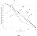
- Figure 6 shows the normalized characteristic parameter values as a function of the etch depth, for four spectroscopy techniques : Raman (curve 30) EDS (curve 31), XPS (curve 32) and SIMS (curve 33), as well as the ratio of the SiGe volume at each depth relative to the SiGe volume at the start of the etch process (curve 34).
- the parameters used are different depending on the spectroscopy technique. For instance, for the Raman curve 30, the ratio was used of the SiGe-related peak in the spectrum, relative to the Si-related peak, as explained above with reference to Figure 2 .
- the parameter is the integrated intensity of the typical Ge-related peak (i.e.
- SIMS the area under the peak in the spectrum that is representative of the SiGe volume.
- three different Ge-related peaks turned out to be representative of the SiGe volume.
- the SIMS-related parameter used in Figure 6 is based on the integrated intensity of one of these three peaks, measured during a sputter time of about 1 hour.
- the XPS curve 32 has one outlier value for the zero-depth measurement point. This is believed to be due to the influence of a thin SiO 2 layer that covers the structures. Apart from this one data point however, it is clear that all these techniques yield a suitable one on one relation between the parameter and the etch depth, that enables to determine the etch depth by measuring the parameter in question.
Landscapes
- Physics & Mathematics (AREA)
- General Physics & Mathematics (AREA)
- Health & Medical Sciences (AREA)
- Chemical & Material Sciences (AREA)
- Nuclear Medicine, Radiotherapy & Molecular Imaging (AREA)
- Life Sciences & Earth Sciences (AREA)
- Analytical Chemistry (AREA)
- Biochemistry (AREA)
- General Health & Medical Sciences (AREA)
- Immunology (AREA)
- Pathology (AREA)
- Electromagnetism (AREA)
- Investigating, Analyzing Materials By Fluorescence Or Luminescence (AREA)
- Testing Or Measuring Of Semiconductors Or The Like (AREA)
- Analysing Materials By The Use Of Radiation (AREA)
Abstract
Description
- The present invention is related to the field of metrology of patterned microstructures produced in semiconductor processing. Within the context of this description, a microstructure is a structure having dimensions of individual features, for example the width and length of a fin, in the order of nanometres up to one or more micrometres.
- The semiconductor processing industry has been driven by scaling of devices, cells and functions to maintain a steady increase in performance per area and cost resulting in device architectures below 10 nm becoming an HVM (High Volume Manufacturing) reality. However, due to their extremely small nmscale dimensions, the manufacturing of the aforementioned devices requires a precise control over their geometry, especially the CD (Critical Dimension). At the same time, technology nodes of 4 nm and beyond will see increased demand for 3D metrology of buried information. In the case of a lateral cavity etch, a certain amount of material is removed laterally, for example below a nitride and/or oxide stack, which greatly hampers accurate control of the etched depth parameter. Such monitoring is commonly done with a metrology step involving Critical Dimension Scanning Electron Microscope (CD-SEM) or Optical Critical Dimension (OCD), but CD-SEM is not sensitive to such buried information and OCD relies on complex models where many geometrical parameters of the complex (oxide, nitride, polysilicon,...) stack may be correlated to the cavity depth such that the latter cannot be uniquely determined by fitting.
- The invention aims to provide a solution to the problems set out in the previous paragraph. This aim is achieved by the methods and by an apparatus as disclosed in the appended claims.
- The method of the invention applies a spectroscopic measurement for determining a lateral recess depth in the sidewall of a microstructure. The structure is formed on a larger substrate with the sidewall in an upright position relative to the substrate, and the recess extends essentially parallel to the substrate. The recess may be an etch depth obtained by etching a first layer relative to two adjacent layers, the layers oriented parallel to the substrate, the etch process progressing inward from the sidewall. According to the method of the invention, an energy beam is directed at the structure. The incident beam falling on the structure generates a spectroscopic response captured and processed respectively by a detector and a processing unit. The response comprises one or more peaks related to the material or materials of the substrate and the structure. According to the invention, a parameter is derived from said one or more peaks, that is representative of the lateral recess depth, said parameter having a previously established one-on-one relation to said depth. From the measured parameter, the depth is derived, using the previously established relation.
- The method is fast and, according to the majority of embodiments, non-invasive and therefore represents a way of performing metrology on buried structures, without the disadvantages of present techniques such as CD-SEM or OCD. The method can be used for in-line measurements of a lateral depth in a semiconductor processing line.
- The invention is in particular related to a method for measuring a lateral recess depth in a microstructure positioned on a substrate, the structure having an elongate sidewall in an upright position relative to the substrate, the structure comprising at least one recess formed from the sidewall inwards and extending essentially parallel to the surface of the substrate, the method comprising the steps of :
- directing an energy beam at the structure,
- measuring a spectroscopic response generated by the interaction between the incident beam and the structure,
- detecting one or more peaks in the response and deriving from said one or more peaks a parameter value that is representative of the recess depth, said parameter having a previously established one-on-one relation to the recess depth,
- deriving the recess depth from the detected parameter value, using the previously established relation.
- According to an embodiment, the structure comprises at least one first layer, oriented essentially parallel to the surface of the substrate, the layer being sandwiched between two adjacent layers, and wherein the first layer is recessed relative to the adjacent layers, the recess being formed from the sidewall inwards.
- According to an embodiment, the first layer is formed of a first material and the adjacent layers are formed of a second material different from the first material.
- According to an embodiment:
- the substrate is a silicon substrate,
- the structure is a fin-shaped structure having two elongate sidewalls, and wherein the first layer and the adjacent layers extend between said two sidewalls,
- the first material is SiGe and the second material is Si,
- the energy beam is a laser beam and the spectroscopic response is a Raman response,
- the fin structure comprises a silicon base portion that is uniform with the substrate, and on said base portion a stack of silicon nanosheets separated from each other and from the base portion by SiGe layers recessed relative to said Si nano-sheets,
- the parameter is the ratio between an intensity peak in the Raman spectrum related to vibrations of silicon atoms in the SiGe layers, and an intensity peak related to vibrations of silicon atoms in the silicon substrate, the base portion and/or the Si nanosheets,
- the previously established relation is linear.
- According to an embodiment, the recess depth is an etch depth, formed in a process wherein the first layer is etched progressively with respect to the adjacent layers, the etch process progressing from the sidewall inwards.
- According to an embodiment, the energy beam is a laser beam, the light of the laser beam being polarized in the length direction of the sidewall, and the spectroscopic response is a Raman spectroscopic response.
- According to an embodiment, the energy beam is an electron beam, and the spectroscopic response is an Energy-Dispersive X-ray Spectroscopy response.
- According to an embodiment, the energy beam is an X-ray beam, and the spectroscopic response is an X-Ray photoelectron Spectroscopy response.
- According to an embodiment, the energy beam is an ion beam, and the spectroscopic response is a Secondary Ion Mass Spectrometry response.
- According to an embodiment, the previously established relation is a linear relation.
- The invention is equally related to an apparatus for performing the method according to the invention, the apparatus comprising :
- An energy beam source,
- A detector,
- A processing unit configured to perform the following steps when the method is applied on a structure as described in appended claim 1 :
- ∘ obtain the spectroscopic response from the detector,
- ∘ determine on the basis of the spectroscopic response, the value of the parameter,
- ∘ derive from the obtained parameter value and from the previously established one-on-one relation, the recess depth.
- According to an embodiment, the source is a laser source and the detector and the processing unit are configured for Raman spectroscopy.
- The invention is equally related to a computer program product configured to run on a processing unit and execute the steps stated in appended
claim 11. - The invention is equally related to a use of the method according to the invention, for performing in-line measurements of lateral recess depth in a semiconductor processing line.
- The invention is equally related to a use of the apparatus according to the invention, for performing in-line measurements of a recess depth in a semiconductor processing line.
-
-
Figures 1a to 1d illustrate progressive stages of an etch process applied on a fin-shaped structure to which the method of the invention is applied. -
Figure 2 shows a typical Raman spectrum obtained by the method of the invention from the structure shown inFigure 1 . -
Figure 3 shows the relation between the ratio of the intensity of two characteristic peaks from the spectrum, and the etch time. -
Figure 4 shows the relation between the same ratio that is represented inFigure 3 , but now as a function of the etch depth. -
Figures 5a and 5b illustrate the application of the method of the invention to an array of forksheet-type fin structures. -
Figure 6 shows the relation between various parameters derived from the method using different spectroscopy techniques, and the etch depth, for the forksheet structures shown inFigures 5a and 5b . - In semiconductor reliability and characterization, spectroscopy is used as a tool for measurements of mechanical stress, composition, doping and phase. Well-known spectroscopic techniques include X-Ray photoelectron spectroscopy (XPS), Energy-dispersive X-ray spectroscopy (EDS) and Raman spectroscopy.
- As stated above and in the claims, the method of the invention allows to measure a lateral depth on the basis of a spectroscopic measurement, wherein a representative parameter is derivable from the response, the parameter being in a previously established one-on-one relation with the depth, thereby allowing to derive the depth from the measurement.
- The invention was verified on the basis of an etch process, but generally the invention is related to measuring a lateral recess depth, regardless of the process by which this depth has been produced. The method may for example also be used to measure progressively the decreasing depth of a lateral cavity, as the cavity is being filled with a filling material.
- The following experiment was conducted and serves as a proof-of-concept of the invention. A fin-shaped
structure 1 was produced, a cross section of which is shown inFigure 1 a. The structure comprises abase portion 2 formed of silicon, that is uniform with asilicon substrate 10. The width of the structure is about 120 nm. The length of the structure measured in the direction perpendicular to the plane of the drawing, is several micrometres. The structure has twosidewalls 11 which may be perpendicular to the surface of thesubstrate 10, as in the drawing, but the walls may also be slightly inclined towards the vertical central plane of thefin structure 1. In general terms, the sidewalls are in an upright position relative to thesubstrate 10. - The
structure 1 further comprises SiGe layers 3 with a thickness of about 9 nm, creating a multistack ofSi nanosheets 4, the nanosheets each also having a thickness of about 9 nm. Asilicon nitride portion 5 on top of the structure represents the lithographic mask used for producing the fin-shapedstructure 1. Thestructure 1 was produced by depositing consecutive thin layers ofSiGe 3 andSi 4 on theSi substrate 10, followed by the formation of thelithographic mask 5 and etching away the materials on either side of the mask down to a depth of about 105 nm measured from the upper surface of theSi substrate 10. The stack of Si and SiGe layers finds an application in the fabrication of superlattice structures in finFET transistors. - The SiGe layers 3 were then etched away by a selective etch process, which may be any process known in the art for this purpose wherein the SiGe is etched progressively inwards from the
sidewalls 11 of the fin-shapedstructure 1, relative to thebase portion 2, themask portion 5, and thesilicon nanosheets 4.Figures 1b, 1c and 1d respectively show the structure at etch times of 10s, 20s and 30s. The lateral etch depth was respectively about 4nm, 10nm and 19nm at these points in time. At each of these etch depths, a Raman spectroscopy measurement was done, using a laser beam oriented perpendicularly with respect to thesubstrate 10 onto which the fin-shapedstructure 1 is positioned. The laser light had a wavelength of 532 nm and was polarized in the direction of the length of thefin structure 1. The laser was focused on a spot having a diameter of about one micrometre (i.e. the laser beam diameter itself was about 1 micrometre), that overlapped the full width of thefin structure 1. The measurement time at each depth was 100s. Generally when applying the Raman-spectroscopy based embodiment of the invention, the measurement time may range from short (for example between 5 and 10s) up to several minutes, depending on the laser power or other parameters. -
Figure 2 shows the Raman response at the start of the etch process, i.e. corresponding to the structure shown inFigure 1a . Thestrong peak 15 at 521 cm-1 is coming from Si-Si vibrations in thesubstrate 10, thebase portion 2 and/or theSi nanosheets 4, but at the same time adistinct satellite peak 16 appears at slightly lower frequency than the main 521 cm-1 peak. This feature originates from Si-Si vibrations in the SiGe material. The intensity of this second peak is a function of the remaining volume of SiGe material, and therefore directly related to the etch depth.Figure 3 shows the Si-Si satellite peak intensity normalized to the Si-Si main peak intensity, i.e. the ratio between thesatellite peak 16 and themain peak 15, as a function of the etch time. A non-linear decrease of the intensity ratio with longer etch time is demonstrated. However when using the total etched depth as the abscissa parameter, as shown inFigure 4 , the relationship becomes linear. This linear relation represents a one-on-one relation between the ratio and the etch depth, i.e. a relation that enables to determine the etch depth when the ratio is known. The relation thus allows to determine the etch depth by measuring the Raman spectrum and deriving from said spectrum the value of the ratio of the satellite peak intensity to the main peak intensity. The method thereby allows to monitor the etch depth by performing regular Raman measurements during the etch process. - The use of the SiGe/Si ratio as the depth-related parameter is itself related to the use of Raman spectroscopy, because it was found that both the SiGe-related
peak 16 and the Si-relatedpeak 15 increase with increasing etch depth, which was unexpected and which may be attributed to the combined effect of a reduction in both the reflectivity and the absorptivity of the sample. The Si-peak however rises faster than the SiGe-related peak, so that the ratio exhibits a reduction as a function of the etch depth. - A similar relation between the Raman peak ratio and the recess depth has been verified on nano-sheet structures of similar dimensions than the ones shown in
Figure 1 , but comprising a stack of SiO2 sheets interspaced with polysilicon sheets having various degrees of recess depths relative to the SiO2 sheets. - Nevertheless, the recess-related parameter may be other than said ratio, which is the case when other spectroscopy techniques are used (see further). In many cases, the recess-related parameter may simply be the intensity of one particular peak in the spectrum, or the integrated area under said peak, the peak being directly representative of the amount of a particular material in the irradiated structure. This parameter then decreases as a function of increasing recess depths. The peak or the integrated peak area is preferably based on a spectrum expressed in arbitrary units (a.u.) as shown in
Figure 2 , said units being independent of the specific measurement conditions applied during the measurement. - The method of the invention is thus not limited to the set of conditions defining the above-described experiment. The method is not applicable only to a fin-shaped
structure 1 wherein the etched layer extends between the twosidewalls 11 of the structure, but generally to any structure having at least one sidewall that is upright with respect to the substrate onto which the structure is formed, with at least one lateral recess extending along the sidewall. The method is applicable to an array of parallel fins, each being recessed from the side in the manner described above. In the latter case, the width of the beam may irradiate several fins of the array. For example, an array of the above-described fin-shaped structures may have a pitch of about 400 nm, so that a laser beam having a diameter of 1 micrometre irradiates two adjacent fins of the array. When the recess-related parameter is the ratio of two peaks as described above, the number of irradiated fins is factored out in the ratio value. However, when the peak value itself, or the integrated area under the peak is used as the depth-related parameter, the number of irradiated fins may need to be taken into account when calculating the recess depth in each of the fins. - The fins may be more narrow than the structure used in the experiment, for example having a width in the order of 20 nm. As stated above, the parameter chosen in the experiment is the ratio between the intensity of the satellite peak relative to the intensity of the main peak. This is true for the particular case of the SiGe layers etched relative to Si. For other geometries and materials, other parameters may be applicable. The method is for example applicable also to similar superlattice structures as in
Figure 1 but with SiO2 and amorphous Si replacing respectively Si and SiGe. The one-on-one relation is preferably linear, which allows the relation to be derived in a wide range of lateral depths, based on only a few calibration measurements. However, also when the relation is not linear, it may be determined across a wide range of depths by a more thorough calibration. The method is therefore not limited to linear relations between the parameter and the lateral depth. - The invention was verified on the basis of an etch process, but generally the invention is related to measuring a lateral recess depth, regardless of the process by which this depth has been produced. The method may for example also be used to measure progressively the decreasing depth of a lateral recess as the recess is being filled with a filling material. For example, when the structure of
Figure 1 is used as a superlattice, the recesses may be filled with a different material, for example TiN to create spacers in between adjacent Si layers. The method of the invention can be used to measure the decreasing depth, based on a spectroscopic response that is sensitive to the progressively increasing volume of said different material in the recesses. In the specific case of spacers filled with TiN, the decreasing depth can for example be detected by the method of the invention, not using Raman spectroscopy which is not suitable for TiN, but using for example EDS (see further). - The invention is not limited to the use of an incident laser beam and analysis via Raman spectroscopy. When this combination is used, the wavelength of the incident light is such that it probes the entire region of interest. It is also important that the laser light is polarized in the length direction of the sidewall or sidewalls of the structure, into which sidewall(s) a lateral recess is formed.
- A number of alternative energy beams and spectroscopic measurement techniques applicable in the invention are summarized hereafter. Using EDS, the energy beam directed at the structure is an electron beam, and the response is measured by detecting X-rays generated by electrons from the beam which excite inner shell electrons in the structure, which then relax and emit X-rays at an energy level that is characteristic for the excited material. The spectroscopic response is therefore a spectrum of X-ray intensity as a function of X-ray energy. For the structure of
Figures 1a-1d , the Ge-related peak in the spectrum is sensitive to the etch depth, with the peak itself or the integrated area under the peak decreasing for increasing recess depths. The landing energy of the e-beam is preferably higher than about 4keV. Successful experiments were done on the structure ofFigure 1 using an e-beam with landing energy of 5.7keV and a measurement time of 60s. - Using XPS, the energy beam directed at the structure is an X-ray beam. The material is ionized through the ejection of inner shell electrons which are detected and whose energy characterizes the material. The spectroscopic response is now a spectrum of emitted electron intensity (electron count) as a function of the binding energy of the inner shell electrons in the various materials, taking into account that the kinetic energy of the emitted electrons is equal to the X-ray energy (known) minus the binding energy. Successful experiments were done on the structure of
Figure 1 , using an aluminium-based X-ray source producing X-rays with energy of 1.48keV, which showed that the 3d Ge-related peak in the spectrum, at a binding energy of about 30eV, is sensitive to the etch depth, with the peak itself or the integrated area under the peak decreasing for increasing recess depths . The measurement time in this case was 2 hours. The use of XPS however does require the removal of thehardmask 5. - Another alternative is the use of Secondary ion mass spectrometry (SIMS), wherein the incident energy beam is an ion beam, which sputters material from the structure in the form of emitted ions, released layer by layer from the structure. The emitted ions are detected and analysed in terms of their mass. The mass is determined e.g. by measuring the time of flight of the ionized species. The spectroscopic response is thus a spectrum of ion counts as a function of the time of flight or the mass of the various materials in the structure. This technique is however invasive as the top layers are sputtered before the signal related to the material at the location of the recess is detected. In relation to this, the measurement time is also longer than the formerly cited techniques. Nevertheless, successful experiments were done on the structure of
Figure 1 , which showed that the Ge-related peaks (Ge-, SiGe-, Ge- 2) in the SIMS spectrum were sensitive to the recess depth, with each of the peaks or the integrated areas under the peaks decreasing for increasing recess depths. The measurement time may be one hour or more, during which time the material is progressively sputtered away from the top of the structures. While sputtering away the SiGe layers 3 during consecutive phases of the total sputter time, the recorded spectra enable to determine the etch depth of the different SiGe layers as the intensity of the Ge-related peaks differs depending on the depth of the respective recesses (i.e. depending on which of the structures shown inFigures 1a to 1d is being subjected to the sputtering beam). - Other existing spectrometry techniques known in the art are usable in the method and in an apparatus of the invention, for example XRF (X-ray fluoresence), XRD (X-ray diffraction analysis) and RBS (Rutherford Backscattering spectrometry).
- The energy beam is not necessarily oriented perpendicularly to the surface of the
substrate 10. The optimal beam orientation may depend on the applied spectroscopy technique. - The invention is not limited to determining the depth of a recess obtainable by removing a layer of a first material, for example the SiGe layers 3 in
Figure 1 , that is sandwiched between two layers of a second material different from the first, such as theSi base portion 2 and the Si-layers 4 inFigure 1 . The recess could be formed in a structure formed of a single material, provided that the spectroscopy technique that is applied is sensitive to the change in volume of this material as a function of the recess depth. - The method of the invention can be applied in-line, for example integrated in a semiconductor manufacturing process that includes a lateral etch process as described above. In this way, the method enables a fast and (in most cases) non-invasive measurement of the etch depth at various times of the etch process, allowing an in-line verification of the etch process.
- The method may be performed using known spectroscopy tools which include an energy beam source, such as a laser or e-beam source, a detector and a processing unit for numerically processing the obtained spectra. The invention is however related also to a specific apparatus for performing the method of the invention, which comprises the same basic components, and wherein the processing unit has access to the previously established relation between the parameter, for example the ratio between the satellite peak intensity and the main peak intensity in the case of the Si/SiGe layer stack, and the recess depth, when the combination laser+Raman spectroscopy is applied. Said relation may be stored in a memory incorporated in or accessible to the processing unit. The processing unit is furthermore configured to perform the following steps :
- obtain the spectroscopic response from the detector,
- determine on the basis of the spectroscopic response obtained from the detector, the value of the parameter,
- derive from the obtained parameter value and from the previously established one-on-one relation, the recess depth.
- Preferably the processing unit is a computer programmed to perform the above steps. The invention is related also to such a computer program as such.
- The method of the invention was applied also to so-called forksheet structures, as illustrated in
Figures 5a and 5b . An array of these forksheet structures was provided, having a critical dimension CD of about 50 nm and a pitch p of about 90nm. As known in the art, forksheet structures are fin-shaped structures comprising nano-sheets, as in the structure ofFigure 1 , but with a vertical wall separating the nano-sheets on either side of the fin's central vertical plane.Forksheet fins 20 as shown inFigure 5a were processed on aSi substrate 10. Each fin comprises alternatingSi nanosheets 21 andSiGe nanosheets 22. The top SiGe nanosheet has a higher thickness than the lower SiGe nanosheets. Thevertical wall 23 comprises SiN, and possibly additional layers not shown in the drawing, but well-known in the art. A layer of STI (Shallow Trench Isolation)oxide 24 separates the structures. The SiGe was etched relative to the Si, resulting in the laterally etched structures shown inFigure 5b . Both the nonetched and the etched structures, at various stages of the etch process corresponding to various etch depths, were subjected to the method of the invention, using a variety of different spectroscopy techniques. -
Figure 6 shows the normalized characteristic parameter values as a function of the etch depth, for four spectroscopy techniques : Raman (curve 30) EDS (curve 31), XPS (curve 32) and SIMS (curve 33), as well as the ratio of the SiGe volume at each depth relative to the SiGe volume at the start of the etch process (curve 34). The parameters used are different depending on the spectroscopy technique. For instance, for theRaman curve 30, the ratio was used of the SiGe-related peak in the spectrum, relative to the Si-related peak, as explained above with reference toFigure 2 . For EDS and XPS, the parameter is the integrated intensity of the typical Ge-related peak (i.e. the area under the peak) in the spectrum that is representative of the SiGe volume. For SIMS, three different Ge-related peaks turned out to be representative of the SiGe volume. The SIMS-related parameter used inFigure 6 is based on the integrated intensity of one of these three peaks, measured during a sputter time of about 1 hour. - It is seen that the
XPS curve 32 has one outlier value for the zero-depth measurement point. This is believed to be due to the influence of a thin SiO2 layer that covers the structures. Apart from this one data point however, it is clear that all these techniques yield a suitable one on one relation between the parameter and the etch depth, that enables to determine the etch depth by measuring the parameter in question. - While the invention has been illustrated and described in detail in the drawings and foregoing description, such illustration and description are to be considered illustrative or exemplary and not restrictive. Other variations to the disclosed embodiments can be understood and effected by those skilled in the art in practicing the claimed invention, from a study of the drawings, the disclosure and the appended claims. In the claims, the word "comprising" does not exclude other elements or steps, and the indefinite article "a" or "an" does not exclude a plurality. The mere fact that certain measures are recited in mutually different dependent claims does not indicate that a combination of these measures cannot be used to advantage. Any reference signs in the claims should not be construed as limiting the scope.
Claims (15)
- A method for measuring a lateral recess depth in a microstructure (1) positioned on a substrate (10), the structure having an elongate sidewall (11) in an upright position relative to the substrate (10), the structure (1) comprising at least one recess formed from the sidewall (11) inwards and extending essentially parallel to the surface of the substrate, the method comprising the steps of :- directing an energy beam at the structure (1),- measuring a spectroscopic response generated by the interaction between the incident beam and the structure (1),- detecting one or more peaks (15,16) in the response and deriving from said one or more peaks a parameter value that is representative of the recess depth, said parameter having a previously established one-on-one relation to the recess depth,- deriving the recess depth from the detected parameter value, using the previously established relation.
- The method according to claim 1, wherein the structure (1) comprises at least one first layer (3), oriented essentially parallel to the surface of the substrate (10), the layer (3) being sandwiched between two adjacent layers (4,2), and wherein the first layer (3) is recessed relative to the adjacent layers (4,2), the recess being formed from the sidewall (11) inwards.
- The method according to claim 2, wherein the first layer (3) is formed of a first material and the adjacent layers (4,2) are formed of a second material different from the first material.
- The method according to claim 3, wherein :- the substrate (10) is a silicon substrate,- the structure (1) is a fin-shaped structure having two elongate sidewalls (11), and wherein the first layer (3,4,2) and the adjacent layers extend between said two sidewalls (11),- the first material is SiGe and the second material is Si,- the energy beam is a laser beam and the spectroscopic response is a Raman response,- the fin structure (1) comprises a silicon base portion (2) that is uniform with the substrate (10), and on said base portion a stack of silicon nanosheets (4) separated from each other and from the base portion (2) by SiGe layers (3) recessed relative to said Si nano-sheets (4),- the parameter is the ratio between an intensity peak (16) in the Raman spectrum related to vibrations of silicon atoms in the SiGe layers (3), and an intensity peak (15) related to vibrations of silicon atoms in the silicon substrate (10), the base portion (2) and/or the Si nanosheets (4),- the previously established relation is linear.
- The method according to any one of claims 2 to 4, wherein the recess depth is an etch depth, formed in a process wherein the first layer (3) is etched progressively with respect to the adjacent layers (4,2), the etch process progressing from the sidewall (11) inwards.
- The method according to any one of the preceding claims, wherein the energy beam is a laser beam, the light of the laser beam being polarized in the length direction of the sidewall (11), and wherein the spectroscopic response is a Raman spectroscopic response.
- The method according to any one of claims 1 to , wherein the energy beam is an electron beam, and wherein the spectroscopic response is an Energy-Dispersive X-ray Spectroscopy response.
- The method according to any one of claims 1 to 3, wherein the energy beam is an X-ray beam, and wherein the spectroscopic response is an X-Ray photoelectron Spectroscopy response.
- The method according to any one of claims 1 to 3, wherein the energy beam is an ion beam, and wherein the spectroscopic response is a Secondary Ion Mass Spectrometry response.
- The method according to any one of the preceding claims, wherein the previously established relation is a linear relation.
- An apparatus for performing the method according to any one of the preceding claims, comprising- An energy beam source,- A detector,- A processing unit configured to perform the following steps when the method is applied on a structure as described in claim 1 :∘ obtain the spectroscopic response from the detector,∘ determine on the basis of the spectroscopic response, the value of the parameter,∘ derive from the obtained parameter value and from the previously established one-on-one relation, the recess depth.
- The apparatus according to claim 11, wherein the source is a laser source and wherein the detector and the processing unit are configured for Raman spectroscopy.
- A computer program product configured to run on a processing unit and execute the steps stated in claim 11.
- Use of the method according to any one of claims 1 to 10, for performing in-line measurements of lateral recess depth in a semiconductor processing line.
- Use of the apparatus according to claim 11 or 12, for performing in-line measurements of a recess depth in a semiconductor processing line.
Applications Claiming Priority (1)
| Application Number | Priority Date | Filing Date | Title |
|---|---|---|---|
| EP20185746 | 2020-07-14 |
Publications (2)
| Publication Number | Publication Date |
|---|---|
| EP3940337A1 true EP3940337A1 (en) | 2022-01-19 |
| EP3940337B1 EP3940337B1 (en) | 2024-01-10 |
Family
ID=71620169
Family Applications (1)
| Application Number | Title | Priority Date | Filing Date |
|---|---|---|---|
| EP21183291.0A Active EP3940337B1 (en) | 2020-07-14 | 2021-07-01 | A method and apparatus for measuring a lateral depth in a microstructure |
Country Status (3)
| Country | Link |
|---|---|
| US (1) | US12216057B2 (en) |
| EP (1) | EP3940337B1 (en) |
| CN (1) | CN113937022A (en) |
Families Citing this family (1)
| Publication number | Priority date | Publication date | Assignee | Title |
|---|---|---|---|---|
| CN114623777B (en) * | 2022-02-21 | 2022-11-18 | 武汉大学 | Construction method and measurement method of measurement model of stacked nanosheet structure |
Citations (4)
| Publication number | Priority date | Publication date | Assignee | Title |
|---|---|---|---|---|
| US20050118735A1 (en) * | 2003-10-09 | 2005-06-02 | Ulrich Mantz | Method for determining or inspecting a property of a patterned layer |
| US20180172609A1 (en) * | 2015-11-02 | 2018-06-21 | Nova Measuring Instruments Ltd. | Method and system for non-destructive metrology of thin layers |
| US20180372644A1 (en) * | 2015-12-15 | 2018-12-27 | Nova Measuring Instruments Ltd. | Raman spectroscopy based measurements in patterned structures |
| US20190178788A1 (en) * | 2017-12-08 | 2019-06-13 | Kla-Tencor Corporation | Measurement Methodology of Advanced Nanostructures |
Family Cites Families (11)
| Publication number | Priority date | Publication date | Assignee | Title |
|---|---|---|---|---|
| JPH0665963B2 (en) * | 1986-09-29 | 1994-08-24 | シャープ株式会社 | Fine groove depth measuring device |
| JP2000292129A (en) * | 1999-04-09 | 2000-10-20 | Toshiba Corp | Etching depth measuring method and apparatus |
| US6582619B1 (en) * | 1999-09-30 | 2003-06-24 | Lam Research Corporation | Methods and apparatuses for trench depth detection and control |
| US7049633B2 (en) * | 1999-12-10 | 2006-05-23 | Tokyo Electron Limited | Method of measuring meso-scale structures on wafers |
| US6650423B1 (en) * | 2001-07-02 | 2003-11-18 | Advanced Micro Devices Inc. | Method and apparatus for determining column dimensions using scatterometry |
| US6940592B2 (en) * | 2001-10-09 | 2005-09-06 | Applied Materials, Inc. | Calibration as well as measurement on the same workpiece during fabrication |
| US20040018647A1 (en) * | 2002-07-02 | 2004-01-29 | Applied Materials, Inc. | Method for controlling the extent of notch or undercut in an etched profile using optical reflectometry |
| US20060077403A1 (en) * | 2004-10-13 | 2006-04-13 | Zaidi Shoaib H | Optical system and method for measuring small dimensions |
| US7839509B2 (en) * | 2005-07-06 | 2010-11-23 | Advanced Metrology Systems Llc | Method of measuring deep trenches with model-based optical spectroscopy |
| CN101393015B (en) * | 2008-10-17 | 2010-06-16 | 华中科技大学 | A method and device for on-line measurement of micro-nano deep groove structure |
| US9059038B2 (en) * | 2012-07-18 | 2015-06-16 | Tokyo Electron Limited | System for in-situ film stack measurement during etching and etch control method |
-
2021
- 2021-07-01 EP EP21183291.0A patent/EP3940337B1/en active Active
- 2021-07-09 US US17/371,609 patent/US12216057B2/en active Active
- 2021-07-13 CN CN202110789468.3A patent/CN113937022A/en active Pending
Patent Citations (4)
| Publication number | Priority date | Publication date | Assignee | Title |
|---|---|---|---|---|
| US20050118735A1 (en) * | 2003-10-09 | 2005-06-02 | Ulrich Mantz | Method for determining or inspecting a property of a patterned layer |
| US20180172609A1 (en) * | 2015-11-02 | 2018-06-21 | Nova Measuring Instruments Ltd. | Method and system for non-destructive metrology of thin layers |
| US20180372644A1 (en) * | 2015-12-15 | 2018-12-27 | Nova Measuring Instruments Ltd. | Raman spectroscopy based measurements in patterned structures |
| US20190178788A1 (en) * | 2017-12-08 | 2019-06-13 | Kla-Tencor Corporation | Measurement Methodology of Advanced Nanostructures |
Non-Patent Citations (1)
| Title |
|---|
| NUYTTEN T ET AL: "Edge-enhanced Raman scattering in narrow sGe fin field-effect transistor channels", APPLIED PHYSICS LETTERS, AMERICAN INSTITUTE OF PHYSICS, 2 HUNTINGTON QUADRANGLE, MELVILLE, NY 11747, vol. 106, no. 3, 19 January 2015 (2015-01-19), XP012193858, ISSN: 0003-6951, [retrieved on 19010101], DOI: 10.1063/1.4906537 * |
Also Published As
| Publication number | Publication date |
|---|---|
| EP3940337B1 (en) | 2024-01-10 |
| CN113937022A (en) | 2022-01-14 |
| US12216057B2 (en) | 2025-02-04 |
| US20220018781A1 (en) | 2022-01-20 |
Similar Documents
| Publication | Publication Date | Title |
|---|---|---|
| US20090296073A1 (en) | Method to create three-dimensional images of semiconductor structures using a focused ion beam device and a scanning electron microscope | |
| KR102081870B1 (en) | Test key design to enable x-ray scatterometry measurement | |
| US12216057B2 (en) | Method and apparatus for measuring a lateral depth in a microstructure | |
| US20020137350A1 (en) | Process of manufacturing electron microscopic sample and process of analyzing semiconductor device | |
| TWI473188B (en) | Determination of etch depth in mask gate trench technology | |
| CN107507787A (en) | A kind of detection method in raceway groove hole | |
| US11199401B1 (en) | End-point detection for similar adjacent materials | |
| Bogdanowicz et al. | Spectroscopy: a new route towards critical-dimension metrology of the cavity etch of nanosheet transistors | |
| CN109883365B (en) | Method for measuring thickness of crystal grain layer and method for judging abnormality of crystal grain layer | |
| KR20150085956A (en) | A method of measuring a semiconductor device, a semiconductor measurement system, and a method of a semiconductor device using the same | |
| US10515818B2 (en) | Semiconductor methods and devices | |
| US20050037625A1 (en) | Site-specific method for large area uniform thickness plan view transmission electron microscopy sample preparation | |
| US6519542B1 (en) | Method of testing an unknown sample with an analytical tool | |
| JP2956627B2 (en) | Impurity concentration analysis method | |
| JP3266050B2 (en) | How to measure concentration profile | |
| Chong et al. | Techniques and Applications of Plasma Focused Ion Beam in Silicon Die Delayering | |
| JP2018157021A (en) | Method of manufacturing semiconductor storage device | |
| US8399834B2 (en) | Isotope ion microscope methods and systems | |
| KR0139577B1 (en) | Method for Fabricating Planar Transmission Electron Microscope Specimen Using Wet Etching Method | |
| Rimini | Analytical Techniques | |
| JPH05190633A (en) | Solid surface elemental analyzer | |
| KR20230009282A (en) | End point control in etching processes | |
| JP5130894B2 (en) | Management method of ion implantation conditions | |
| CN113643996A (en) | Methods of Characterization of Density | |
| Garud | Shallow trench isolation process in microfabrication for flash (NAND) memory |
Legal Events
| Date | Code | Title | Description |
|---|---|---|---|
| PUAI | Public reference made under article 153(3) epc to a published international application that has entered the european phase |
Free format text: ORIGINAL CODE: 0009012 |
|
| STAA | Information on the status of an ep patent application or granted ep patent |
Free format text: STATUS: THE APPLICATION HAS BEEN PUBLISHED |
|
| AK | Designated contracting states |
Kind code of ref document: A1 Designated state(s): AL AT BE BG CH CY CZ DE DK EE ES FI FR GB GR HR HU IE IS IT LI LT LU LV MC MK MT NL NO PL PT RO RS SE SI SK SM TR |
|
| STAA | Information on the status of an ep patent application or granted ep patent |
Free format text: STATUS: REQUEST FOR EXAMINATION WAS MADE |
|
| 17P | Request for examination filed |
Effective date: 20220714 |
|
| RBV | Designated contracting states (corrected) |
Designated state(s): AL AT BE BG CH CY CZ DE DK EE ES FI FR GB GR HR HU IE IS IT LI LT LU LV MC MK MT NL NO PL PT RO RS SE SI SK SM TR |
|
| GRAP | Despatch of communication of intention to grant a patent |
Free format text: ORIGINAL CODE: EPIDOSNIGR1 |
|
| STAA | Information on the status of an ep patent application or granted ep patent |
Free format text: STATUS: GRANT OF PATENT IS INTENDED |
|
| RIC1 | Information provided on ipc code assigned before grant |
Ipc: G03F 7/00 20060101ALN20230804BHEP Ipc: H01L 29/775 20060101ALI20230804BHEP Ipc: H01L 29/06 20060101ALI20230804BHEP Ipc: G03F 7/20 20060101ALI20230804BHEP Ipc: G01B 15/00 20060101ALI20230804BHEP Ipc: G01B 11/22 20060101AFI20230804BHEP |
|
| INTG | Intention to grant announced |
Effective date: 20230905 |
|
| P01 | Opt-out of the competence of the unified patent court (upc) registered |
Effective date: 20230914 |
|
| GRAS | Grant fee paid |
Free format text: ORIGINAL CODE: EPIDOSNIGR3 |
|
| GRAA | (expected) grant |
Free format text: ORIGINAL CODE: 0009210 |
|
| STAA | Information on the status of an ep patent application or granted ep patent |
Free format text: STATUS: THE PATENT HAS BEEN GRANTED |
|
| AK | Designated contracting states |
Kind code of ref document: B1 Designated state(s): AL AT BE BG CH CY CZ DE DK EE ES FI FR GB GR HR HU IE IS IT LI LT LU LV MC MK MT NL NO PL PT RO RS SE SI SK SM TR |
|
| REG | Reference to a national code |
Ref country code: GB Ref legal event code: FG4D |
|
| REG | Reference to a national code |
Ref country code: CH Ref legal event code: EP |
|
| REG | Reference to a national code |
Ref country code: DE Ref legal event code: R096 Ref document number: 602021008462 Country of ref document: DE |
|
| REG | Reference to a national code |
Ref country code: IE Ref legal event code: FG4D |
|
| REG | Reference to a national code |
Ref country code: LT Ref legal event code: MG9D |
|
| REG | Reference to a national code |
Ref country code: NL Ref legal event code: MP Effective date: 20240110 |
|
| REG | Reference to a national code |
Ref country code: AT Ref legal event code: MK05 Ref document number: 1649219 Country of ref document: AT Kind code of ref document: T Effective date: 20240110 |
|
| PG25 | Lapsed in a contracting state [announced via postgrant information from national office to epo] |
Ref country code: NL Free format text: LAPSE BECAUSE OF FAILURE TO SUBMIT A TRANSLATION OF THE DESCRIPTION OR TO PAY THE FEE WITHIN THE PRESCRIBED TIME-LIMIT Effective date: 20240110 |
|
| PG25 | Lapsed in a contracting state [announced via postgrant information from national office to epo] |
Ref country code: NL Free format text: LAPSE BECAUSE OF FAILURE TO SUBMIT A TRANSLATION OF THE DESCRIPTION OR TO PAY THE FEE WITHIN THE PRESCRIBED TIME-LIMIT Effective date: 20240110 |
|
| PG25 | Lapsed in a contracting state [announced via postgrant information from national office to epo] |
Ref country code: IS Free format text: LAPSE BECAUSE OF FAILURE TO SUBMIT A TRANSLATION OF THE DESCRIPTION OR TO PAY THE FEE WITHIN THE PRESCRIBED TIME-LIMIT Effective date: 20240510 |
|
| PG25 | Lapsed in a contracting state [announced via postgrant information from national office to epo] |
Ref country code: LT Free format text: LAPSE BECAUSE OF FAILURE TO SUBMIT A TRANSLATION OF THE DESCRIPTION OR TO PAY THE FEE WITHIN THE PRESCRIBED TIME-LIMIT Effective date: 20240110 |
|
| PG25 | Lapsed in a contracting state [announced via postgrant information from national office to epo] |
Ref country code: GR Free format text: LAPSE BECAUSE OF FAILURE TO SUBMIT A TRANSLATION OF THE DESCRIPTION OR TO PAY THE FEE WITHIN THE PRESCRIBED TIME-LIMIT Effective date: 20240411 |
|
| PG25 | Lapsed in a contracting state [announced via postgrant information from national office to epo] |
Ref country code: RS Free format text: LAPSE BECAUSE OF FAILURE TO SUBMIT A TRANSLATION OF THE DESCRIPTION OR TO PAY THE FEE WITHIN THE PRESCRIBED TIME-LIMIT Effective date: 20240410 Ref country code: HR Free format text: LAPSE BECAUSE OF FAILURE TO SUBMIT A TRANSLATION OF THE DESCRIPTION OR TO PAY THE FEE WITHIN THE PRESCRIBED TIME-LIMIT Effective date: 20240110 |
|
| PG25 | Lapsed in a contracting state [announced via postgrant information from national office to epo] |
Ref country code: ES Free format text: LAPSE BECAUSE OF FAILURE TO SUBMIT A TRANSLATION OF THE DESCRIPTION OR TO PAY THE FEE WITHIN THE PRESCRIBED TIME-LIMIT Effective date: 20240110 |
|
| PG25 | Lapsed in a contracting state [announced via postgrant information from national office to epo] |
Ref country code: AT Free format text: LAPSE BECAUSE OF FAILURE TO SUBMIT A TRANSLATION OF THE DESCRIPTION OR TO PAY THE FEE WITHIN THE PRESCRIBED TIME-LIMIT Effective date: 20240110 |
|
| PG25 | Lapsed in a contracting state [announced via postgrant information from national office to epo] |
Ref country code: RS Free format text: LAPSE BECAUSE OF FAILURE TO SUBMIT A TRANSLATION OF THE DESCRIPTION OR TO PAY THE FEE WITHIN THE PRESCRIBED TIME-LIMIT Effective date: 20240410 Ref country code: NO Free format text: LAPSE BECAUSE OF FAILURE TO SUBMIT A TRANSLATION OF THE DESCRIPTION OR TO PAY THE FEE WITHIN THE PRESCRIBED TIME-LIMIT Effective date: 20240410 Ref country code: LT Free format text: LAPSE BECAUSE OF FAILURE TO SUBMIT A TRANSLATION OF THE DESCRIPTION OR TO PAY THE FEE WITHIN THE PRESCRIBED TIME-LIMIT Effective date: 20240110 Ref country code: IS Free format text: LAPSE BECAUSE OF FAILURE TO SUBMIT A TRANSLATION OF THE DESCRIPTION OR TO PAY THE FEE WITHIN THE PRESCRIBED TIME-LIMIT Effective date: 20240510 Ref country code: HR Free format text: LAPSE BECAUSE OF FAILURE TO SUBMIT A TRANSLATION OF THE DESCRIPTION OR TO PAY THE FEE WITHIN THE PRESCRIBED TIME-LIMIT Effective date: 20240110 Ref country code: GR Free format text: LAPSE BECAUSE OF FAILURE TO SUBMIT A TRANSLATION OF THE DESCRIPTION OR TO PAY THE FEE WITHIN THE PRESCRIBED TIME-LIMIT Effective date: 20240411 Ref country code: ES Free format text: LAPSE BECAUSE OF FAILURE TO SUBMIT A TRANSLATION OF THE DESCRIPTION OR TO PAY THE FEE WITHIN THE PRESCRIBED TIME-LIMIT Effective date: 20240110 Ref country code: BG Free format text: LAPSE BECAUSE OF FAILURE TO SUBMIT A TRANSLATION OF THE DESCRIPTION OR TO PAY THE FEE WITHIN THE PRESCRIBED TIME-LIMIT Effective date: 20240110 Ref country code: AT Free format text: LAPSE BECAUSE OF FAILURE TO SUBMIT A TRANSLATION OF THE DESCRIPTION OR TO PAY THE FEE WITHIN THE PRESCRIBED TIME-LIMIT Effective date: 20240110 |
|
| PG25 | Lapsed in a contracting state [announced via postgrant information from national office to epo] |
Ref country code: PL Free format text: LAPSE BECAUSE OF FAILURE TO SUBMIT A TRANSLATION OF THE DESCRIPTION OR TO PAY THE FEE WITHIN THE PRESCRIBED TIME-LIMIT Effective date: 20240110 Ref country code: PT Free format text: LAPSE BECAUSE OF FAILURE TO SUBMIT A TRANSLATION OF THE DESCRIPTION OR TO PAY THE FEE WITHIN THE PRESCRIBED TIME-LIMIT Effective date: 20240510 |
|
| PG25 | Lapsed in a contracting state [announced via postgrant information from national office to epo] |
Ref country code: SE Free format text: LAPSE BECAUSE OF FAILURE TO SUBMIT A TRANSLATION OF THE DESCRIPTION OR TO PAY THE FEE WITHIN THE PRESCRIBED TIME-LIMIT Effective date: 20240110 Ref country code: PT Free format text: LAPSE BECAUSE OF FAILURE TO SUBMIT A TRANSLATION OF THE DESCRIPTION OR TO PAY THE FEE WITHIN THE PRESCRIBED TIME-LIMIT Effective date: 20240510 Ref country code: PL Free format text: LAPSE BECAUSE OF FAILURE TO SUBMIT A TRANSLATION OF THE DESCRIPTION OR TO PAY THE FEE WITHIN THE PRESCRIBED TIME-LIMIT Effective date: 20240110 Ref country code: LV Free format text: LAPSE BECAUSE OF FAILURE TO SUBMIT A TRANSLATION OF THE DESCRIPTION OR TO PAY THE FEE WITHIN THE PRESCRIBED TIME-LIMIT Effective date: 20240110 |
|
| PG25 | Lapsed in a contracting state [announced via postgrant information from national office to epo] |
Ref country code: DK Free format text: LAPSE BECAUSE OF FAILURE TO SUBMIT A TRANSLATION OF THE DESCRIPTION OR TO PAY THE FEE WITHIN THE PRESCRIBED TIME-LIMIT Effective date: 20240110 |
|
| REG | Reference to a national code |
Ref country code: DE Ref legal event code: R097 Ref document number: 602021008462 Country of ref document: DE |
|
| PG25 | Lapsed in a contracting state [announced via postgrant information from national office to epo] |
Ref country code: SM Free format text: LAPSE BECAUSE OF FAILURE TO SUBMIT A TRANSLATION OF THE DESCRIPTION OR TO PAY THE FEE WITHIN THE PRESCRIBED TIME-LIMIT Effective date: 20240110 |
|
| PG25 | Lapsed in a contracting state [announced via postgrant information from national office to epo] |
Ref country code: EE Free format text: LAPSE BECAUSE OF FAILURE TO SUBMIT A TRANSLATION OF THE DESCRIPTION OR TO PAY THE FEE WITHIN THE PRESCRIBED TIME-LIMIT Effective date: 20240110 Ref country code: CZ Free format text: LAPSE BECAUSE OF FAILURE TO SUBMIT A TRANSLATION OF THE DESCRIPTION OR TO PAY THE FEE WITHIN THE PRESCRIBED TIME-LIMIT Effective date: 20240110 |
|
| PG25 | Lapsed in a contracting state [announced via postgrant information from national office to epo] |
Ref country code: SK Free format text: LAPSE BECAUSE OF FAILURE TO SUBMIT A TRANSLATION OF THE DESCRIPTION OR TO PAY THE FEE WITHIN THE PRESCRIBED TIME-LIMIT Effective date: 20240110 |
|
| PG25 | Lapsed in a contracting state [announced via postgrant information from national office to epo] |
Ref country code: SM Free format text: LAPSE BECAUSE OF FAILURE TO SUBMIT A TRANSLATION OF THE DESCRIPTION OR TO PAY THE FEE WITHIN THE PRESCRIBED TIME-LIMIT Effective date: 20240110 Ref country code: SK Free format text: LAPSE BECAUSE OF FAILURE TO SUBMIT A TRANSLATION OF THE DESCRIPTION OR TO PAY THE FEE WITHIN THE PRESCRIBED TIME-LIMIT Effective date: 20240110 Ref country code: RO Free format text: LAPSE BECAUSE OF FAILURE TO SUBMIT A TRANSLATION OF THE DESCRIPTION OR TO PAY THE FEE WITHIN THE PRESCRIBED TIME-LIMIT Effective date: 20240110 Ref country code: EE Free format text: LAPSE BECAUSE OF FAILURE TO SUBMIT A TRANSLATION OF THE DESCRIPTION OR TO PAY THE FEE WITHIN THE PRESCRIBED TIME-LIMIT Effective date: 20240110 Ref country code: DK Free format text: LAPSE BECAUSE OF FAILURE TO SUBMIT A TRANSLATION OF THE DESCRIPTION OR TO PAY THE FEE WITHIN THE PRESCRIBED TIME-LIMIT Effective date: 20240110 Ref country code: CZ Free format text: LAPSE BECAUSE OF FAILURE TO SUBMIT A TRANSLATION OF THE DESCRIPTION OR TO PAY THE FEE WITHIN THE PRESCRIBED TIME-LIMIT Effective date: 20240110 |
|
| PLBE | No opposition filed within time limit |
Free format text: ORIGINAL CODE: 0009261 |
|
| STAA | Information on the status of an ep patent application or granted ep patent |
Free format text: STATUS: NO OPPOSITION FILED WITHIN TIME LIMIT |
|
| PG25 | Lapsed in a contracting state [announced via postgrant information from national office to epo] |
Ref country code: IT Free format text: LAPSE BECAUSE OF FAILURE TO SUBMIT A TRANSLATION OF THE DESCRIPTION OR TO PAY THE FEE WITHIN THE PRESCRIBED TIME-LIMIT Effective date: 20240110 |
|
| 26N | No opposition filed |
Effective date: 20241011 |
|
| PG25 | Lapsed in a contracting state [announced via postgrant information from national office to epo] |
Ref country code: IT Free format text: LAPSE BECAUSE OF FAILURE TO SUBMIT A TRANSLATION OF THE DESCRIPTION OR TO PAY THE FEE WITHIN THE PRESCRIBED TIME-LIMIT Effective date: 20240110 |
|
| PG25 | Lapsed in a contracting state [announced via postgrant information from national office to epo] |
Ref country code: MC Free format text: LAPSE BECAUSE OF FAILURE TO SUBMIT A TRANSLATION OF THE DESCRIPTION OR TO PAY THE FEE WITHIN THE PRESCRIBED TIME-LIMIT Effective date: 20240110 |
|
| REG | Reference to a national code |
Ref country code: CH Ref legal event code: PL |
|
| PG25 | Lapsed in a contracting state [announced via postgrant information from national office to epo] |
Ref country code: LU Free format text: LAPSE BECAUSE OF NON-PAYMENT OF DUE FEES Effective date: 20240701 |
|
| PG25 | Lapsed in a contracting state [announced via postgrant information from national office to epo] |
Ref country code: LU Free format text: LAPSE BECAUSE OF NON-PAYMENT OF DUE FEES Effective date: 20240701 |
|
| PG25 | Lapsed in a contracting state [announced via postgrant information from national office to epo] |
Ref country code: CH Free format text: LAPSE BECAUSE OF NON-PAYMENT OF DUE FEES Effective date: 20240731 Ref country code: BE Free format text: LAPSE BECAUSE OF NON-PAYMENT OF DUE FEES Effective date: 20240731 Ref country code: SI Free format text: LAPSE BECAUSE OF FAILURE TO SUBMIT A TRANSLATION OF THE DESCRIPTION OR TO PAY THE FEE WITHIN THE PRESCRIBED TIME-LIMIT Effective date: 20240110 |
|
| PG25 | Lapsed in a contracting state [announced via postgrant information from national office to epo] |
Ref country code: FR Free format text: LAPSE BECAUSE OF NON-PAYMENT OF DUE FEES Effective date: 20240731 |
|
| REG | Reference to a national code |
Ref country code: BE Ref legal event code: MM Effective date: 20240731 |
|
| PG25 | Lapsed in a contracting state [announced via postgrant information from national office to epo] |
Ref country code: IE Free format text: LAPSE BECAUSE OF NON-PAYMENT OF DUE FEES Effective date: 20240701 |
|
| PG25 | Lapsed in a contracting state [announced via postgrant information from national office to epo] |
Ref country code: FI Free format text: LAPSE BECAUSE OF FAILURE TO SUBMIT A TRANSLATION OF THE DESCRIPTION OR TO PAY THE FEE WITHIN THE PRESCRIBED TIME-LIMIT Effective date: 20240110 |
|
| PGFP | Annual fee paid to national office [announced via postgrant information from national office to epo] |
Ref country code: DE Payment date: 20250620 Year of fee payment: 5 |
|
| PG25 | Lapsed in a contracting state [announced via postgrant information from national office to epo] |
Ref country code: CY Free format text: LAPSE BECAUSE OF FAILURE TO SUBMIT A TRANSLATION OF THE DESCRIPTION OR TO PAY THE FEE WITHIN THE PRESCRIBED TIME-LIMIT; INVALID AB INITIO Effective date: 20210701 |
|
| PG25 | Lapsed in a contracting state [announced via postgrant information from national office to epo] |
Ref country code: HU Free format text: LAPSE BECAUSE OF FAILURE TO SUBMIT A TRANSLATION OF THE DESCRIPTION OR TO PAY THE FEE WITHIN THE PRESCRIBED TIME-LIMIT; INVALID AB INITIO Effective date: 20210701 |
|
| GBPC | Gb: european patent ceased through non-payment of renewal fee |
Effective date: 20250701 |
|
| PG25 | Lapsed in a contracting state [announced via postgrant information from national office to epo] |
Ref country code: GB Free format text: LAPSE BECAUSE OF NON-PAYMENT OF DUE FEES Effective date: 20250701 |