EP3938875B1 - Force sensing touch panel - Google Patents
Force sensing touch panel Download PDFInfo
- Publication number
- EP3938875B1 EP3938875B1 EP20715124.2A EP20715124A EP3938875B1 EP 3938875 B1 EP3938875 B1 EP 3938875B1 EP 20715124 A EP20715124 A EP 20715124A EP 3938875 B1 EP3938875 B1 EP 3938875B1
- Authority
- EP
- European Patent Office
- Prior art keywords
- electrodes
- touch panel
- capacitance
- sensing
- sensing electrodes
- Prior art date
- Legal status (The legal status is an assumption and is not a legal conclusion. Google has not performed a legal analysis and makes no representation as to the accuracy of the status listed.)
- Active
Links
Images





Classifications
-
- G—PHYSICS
- G06—COMPUTING OR CALCULATING; COUNTING
- G06F—ELECTRIC DIGITAL DATA PROCESSING
- G06F3/00—Input arrangements for transferring data to be processed into a form capable of being handled by the computer; Output arrangements for transferring data from processing unit to output unit, e.g. interface arrangements
- G06F3/01—Input arrangements or combined input and output arrangements for interaction between user and computer
- G06F3/03—Arrangements for converting the position or the displacement of a member into a coded form
- G06F3/041—Digitisers, e.g. for touch screens or touch pads, characterised by the transducing means
- G06F3/044—Digitisers, e.g. for touch screens or touch pads, characterised by the transducing means by capacitive means
- G06F3/0443—Digitisers, e.g. for touch screens or touch pads, characterised by the transducing means by capacitive means using a single layer of sensing electrodes
-
- G—PHYSICS
- G06—COMPUTING OR CALCULATING; COUNTING
- G06F—ELECTRIC DIGITAL DATA PROCESSING
- G06F3/00—Input arrangements for transferring data to be processed into a form capable of being handled by the computer; Output arrangements for transferring data from processing unit to output unit, e.g. interface arrangements
- G06F3/01—Input arrangements or combined input and output arrangements for interaction between user and computer
- G06F3/03—Arrangements for converting the position or the displacement of a member into a coded form
- G06F3/041—Digitisers, e.g. for touch screens or touch pads, characterised by the transducing means
- G06F3/0412—Digitisers structurally integrated in a display
-
- G—PHYSICS
- G06—COMPUTING OR CALCULATING; COUNTING
- G06F—ELECTRIC DIGITAL DATA PROCESSING
- G06F3/00—Input arrangements for transferring data to be processed into a form capable of being handled by the computer; Output arrangements for transferring data from processing unit to output unit, e.g. interface arrangements
- G06F3/01—Input arrangements or combined input and output arrangements for interaction between user and computer
- G06F3/03—Arrangements for converting the position or the displacement of a member into a coded form
- G06F3/041—Digitisers, e.g. for touch screens or touch pads, characterised by the transducing means
- G06F3/0414—Digitisers, e.g. for touch screens or touch pads, characterised by the transducing means using force sensing means to determine a position
-
- G—PHYSICS
- G06—COMPUTING OR CALCULATING; COUNTING
- G06F—ELECTRIC DIGITAL DATA PROCESSING
- G06F3/00—Input arrangements for transferring data to be processed into a form capable of being handled by the computer; Output arrangements for transferring data from processing unit to output unit, e.g. interface arrangements
- G06F3/01—Input arrangements or combined input and output arrangements for interaction between user and computer
- G06F3/03—Arrangements for converting the position or the displacement of a member into a coded form
- G06F3/041—Digitisers, e.g. for touch screens or touch pads, characterised by the transducing means
- G06F3/0416—Control or interface arrangements specially adapted for digitisers
- G06F3/04164—Connections between sensors and controllers, e.g. routing lines between electrodes and connection pads
-
- G—PHYSICS
- G06—COMPUTING OR CALCULATING; COUNTING
- G06F—ELECTRIC DIGITAL DATA PROCESSING
- G06F3/00—Input arrangements for transferring data to be processed into a form capable of being handled by the computer; Output arrangements for transferring data from processing unit to output unit, e.g. interface arrangements
- G06F3/01—Input arrangements or combined input and output arrangements for interaction between user and computer
- G06F3/03—Arrangements for converting the position or the displacement of a member into a coded form
- G06F3/041—Digitisers, e.g. for touch screens or touch pads, characterised by the transducing means
- G06F3/044—Digitisers, e.g. for touch screens or touch pads, characterised by the transducing means by capacitive means
- G06F3/0445—Digitisers, e.g. for touch screens or touch pads, characterised by the transducing means by capacitive means using two or more layers of sensing electrodes, e.g. using two layers of electrodes separated by a dielectric layer
-
- G—PHYSICS
- G06—COMPUTING OR CALCULATING; COUNTING
- G06F—ELECTRIC DIGITAL DATA PROCESSING
- G06F3/00—Input arrangements for transferring data to be processed into a form capable of being handled by the computer; Output arrangements for transferring data from processing unit to output unit, e.g. interface arrangements
- G06F3/01—Input arrangements or combined input and output arrangements for interaction between user and computer
- G06F3/03—Arrangements for converting the position or the displacement of a member into a coded form
- G06F3/041—Digitisers, e.g. for touch screens or touch pads, characterised by the transducing means
- G06F3/044—Digitisers, e.g. for touch screens or touch pads, characterised by the transducing means by capacitive means
- G06F3/0446—Digitisers, e.g. for touch screens or touch pads, characterised by the transducing means by capacitive means using a grid-like structure of electrodes in at least two directions, e.g. using row and column electrodes
-
- G—PHYSICS
- G06—COMPUTING OR CALCULATING; COUNTING
- G06F—ELECTRIC DIGITAL DATA PROCESSING
- G06F3/00—Input arrangements for transferring data to be processed into a form capable of being handled by the computer; Output arrangements for transferring data from processing unit to output unit, e.g. interface arrangements
- G06F3/01—Input arrangements or combined input and output arrangements for interaction between user and computer
- G06F3/03—Arrangements for converting the position or the displacement of a member into a coded form
- G06F3/041—Digitisers, e.g. for touch screens or touch pads, characterised by the transducing means
- G06F3/044—Digitisers, e.g. for touch screens or touch pads, characterised by the transducing means by capacitive means
- G06F3/0447—Position sensing using the local deformation of sensor cells
-
- G—PHYSICS
- G06—COMPUTING OR CALCULATING; COUNTING
- G06F—ELECTRIC DIGITAL DATA PROCESSING
- G06F2203/00—Indexing scheme relating to G06F3/00 - G06F3/048
- G06F2203/041—Indexing scheme relating to G06F3/041 - G06F3/045
- G06F2203/04106—Multi-sensing digitiser, i.e. digitiser using at least two different sensing technologies simultaneously or alternatively, e.g. for detecting pen and finger, for saving power or for improving position detection
Definitions
- the present invention relates to a touch panel for force sensing.
- Resistive and capacitive touch panels are used as input devices for computers and mobile devices.
- One type of capacitive touch panel, projected capacitance touch panels is often used for mobile devices because an exterior layer may be made of glass, providing a hard surface which is resistant to scratching.
- An example of a projected capacitance touch panel is described in US 2010/0079384 A1 .
- JP 2010-026938 A describes a touch panel which includes a piezoelectric body layer containing a polyvinylidene fluoride-ethylene tetrafluoride copolymer, a first electrode provided on one surface of the piezoelectric body layer, and a second electrode provided on the other surface of the piezoelectric body layer.
- touch sensors combining capacitive sensing with piezoelectric based force-detection capabilities are described in WO 2016/102975 A1 . Further examples of touch sensors combining capacitive sensing with piezoelectric based force-detection capabilities are described in WO 2017/109455 A1 , WO 2019/030513 A1 and US 2017/262099 A1 .
- US2018/0059866 A1 discloses a touch panel using capacitive touch and force detection to discriminate between intended touches, including when the user is wearing gloves, and unintended touches or contamination of the touch panel caused by water.
- US2018/0341347 A1 discloses a touch panel using acoustic touch and force detection that can detect touches even when the panel is wet or submerged.
- apparatus which includes a touch panel.
- the touch panel includes a layer of piezoelectric material disposed between a number of sensing electrodes and at least one counter electrode.
- the apparatus also includes a touch controller connected to the touch panel.
- the touch controller is configured to determine, in response to receiving piezoelectric signals from one or more of the sensing electrodes, a location and an applied force corresponding to a user interaction with the touch panel.
- the touch controller is configured, in response to receiving piezoelectric signals and determining no changes in the capacitance values for any of the sensing electrodes, to operate in a force-based mode wherein the touch controller is configured to determine a location and an applied force corresponding to a user interaction based on the piezoelectric signals.
- the touch controller is configured, in response to determining changes in the capacitance values of one or more sensing electrodes and receiving no piezoelectric signals, to operate in a capacitance-based mode wherein the touch controller is configured to determine a location corresponding to a user interaction based on the determined changes in capacitance values.
- the touch controller is configured, in response to determining changes in the capacitance values of one or more sensing electrodes and receiving piezoelectric signals, to operate in a mixed force-capacitance mode wherein the touch controller is configured to determine a location corresponding to a user interaction based on the determined changes in capacitance values and to determine an applied force corresponding to the user interaction based on the piezoelectric signals.
- Each sensing electrode may include one or more sensing pads. Each sensing pad may be opposed across the layer of piezoelectric material by a corresponding counter electrode pad of a counter electrode.
- the touch controller may also be configured to determine a capacitance value of one or more of the sensing electrodes.
- the touch controller may be configured to determine one or more capacitance values and to receive one or more piezoelectric signals concurrently.
- the touch controller may be configured to determine one or more capacitance values and to receive one or more piezoelectric signals sequentially.
- the touch controller may be configured to determine a location corresponding to a user interaction based on the determined changes in the capacitance values and the piezoelectric signals.
- the touch controller may also be configured to determine whether the touch panel is wet or submerged based on the determined capacitance values of the sensing electrodes.
- the touch controller may also be configured, in response to determining that the touch panel is wet, to operate in the force-based mode.
- the touch controller may also be configured to operate in the force-based mode in response to determining that a signal-to-noise ratio of the capacitance values is less than a pre-calibrated threshold.
- the apparatus may also include a switch configured such that when the touch controller operates in the force-based mode, the switch connects each sensing electrode to a corresponding piezoelectric signal sensing circuit.
- the switch may be configured such that when the touch controller operates in the mixed force-capacitance mode, the switch connects two or more sensing electrodes to one piezoelectric signal sensing circuit.
- the sensing electrodes may include a number of first electrodes and a number of second electrodes. Each first electrode may extend in a first direction, and the first electrodes may be spaced apart in a second direction which is perpendicular to the first direction. Each second electrode may extend in the second direction, and the plurality of second electrodes may be spaced apart in the first direction.
- the first and second electrodes may be arranged on the same plane within the touch panel.
- the first and second electrodes may be arranged on different, parallel planes within the touch panel.
- the touch panel may have a circular or elliptical perimeter.
- the touch panel may have a square or rectangular perimeter.
- the touch panel may be a button input panel.
- a button input panel may include one or more sensing electrodes in the form of discrete button electrodes. Button electrodes of the button input panel may have different sizes and/or shapes.
- the counter electrode of the button input panel may be uniform.
- the counter electrode of the button input panel may be patterned to match the shapes and positions of the button electrodes. Patterned counter electrodes may all be electrically connected to one another. Patterned counter electrodes may be connected to individual conductive traces to enable patterned counter electrodes to be addressed individually.
- the button input panel may include a light emitting diode layer including one or more light emitting diodes. Each light emitting diode may be disposed and configured to illuminate a corresponding button electrode.
- a wearable device may include the apparatus.
- a wearable device may take the form of a watch, a smart watch, a bracelet, a belt, a buckle, glasses, lenses of glasses, frames of glasses, jewellery, and so forth.
- a method for processing signals from a touch panel includes a layer of piezoelectric material disposed between a plurality of sensing electrodes and at least one counter electrode.
- the method includes, in response to receiving piezoelectric signals from one or more of the sensing electrodes, determining a location corresponding to a user interaction with the touch panel based on the piezoelectric signals.
- the method also includes determining a capacitance value of one or more of the sensing electrodes.
- the method also includes, in response to receiving piezoelectric signals and determining no changes in the capacitance values for any of the sensing electrodes, determining, in a force-based mode, a location and an applied force corresponding to a user interaction based on the piezoelectric signals.
- the method also includes, in response to determining changes in the capacitance values of one or more sensing electrodes and receiving no piezoelectric signals, determining, in a capacitance-based mode, a location corresponding to a user interaction based on the determined changes in capacitance values.
- the method also includes, in response to determining changes in the capacitance values of one or more sensing electrodes and receiving piezoelectric signals, determining, in a mixed force-capacitance mode, a location corresponding to a user interaction based on the determined changes in capacitance values and determining an applied force corresponding to the user interaction based on the piezoelectric signals.
- Determining capacitance values of one or more of the sensing electrodes may be performed concurrently with receiving piezoelectric signals from one or more of the sensing electrodes.
- Determining capacitance values of one or more of the sensing electrodes may be performed sequentially with receiving piezoelectric signals from one or more of the sensing electrodes. Sequentially may include alternating between determining capacitance values and receiving piezoelectric signals.
- the location corresponding to a user interaction may be determined based on the determined changes in capacitance values and the piezoelectric signals.
- the method may also include determining whether the touch panel is wet or submerged based on the determined capacitance values of the sensing electrodes. The method may also include, in response to determining that the touch panel is wet, operating in the force-based mode.
- the method may also include operating in the force-based mode in response to determining that a signal-to-noise ratio of the capacitance values is less than a pre-calibrated threshold.
- the touch panel may be a button input panel.
- a button input panel may include one or more sensing electrodes in the form of discrete button electrodes. Button electrodes of the button input panel may have different sizes and/or shapes.
- the counter electrode of the button input panel may be uniform.
- the counter electrode of the button input panel may be patterned to match the shapes and positions of the button electrodes. Patterned counter electrodes may all be electrically connected to one another. Patterned counter electrodes may be connected to individual conductive traces to enable patterned counter electrodes to be addressed individually.
- the button input panel may include a light emitting diode layer including one or more light emitting diodes. Each light emitting diode may be disposed and configured to illuminate a corresponding button electrode.
- Projected capacitance touch panels operate by detecting changes in electric fields caused by the proximity of a conductive object. However, when a projected capacitance screen is wet, or fully submerged, the presence of water may cause the determination of a number of and locations of user touches based on capacitance values to become unreliable or entirely non-functional.
- Touch panels which operate using combined force sensing and capacitance sensing may use the capacitance measurements to determine the locations of one or more touches.
- capacitance measurements suffer the same issues as a pure capacitive touch panel when wet or submerged underwater.
- capacitance measurements will not detect a user touch using a non-conductive object, or through most conventional gloves.
- the present specification concerns apparatuses and methods which may mitigate one or more of these issues.
- FIG. 1 a schematic cross section of a display stack-up including a first touch panel 1 is shown.
- the first apparatus 2 includes the first touch panel 1 and a touch controller 3.
- the touch panel 1 includes a layer of piezoelectric material 4 disposed between a number of sensing electrodes 5 and at least one counter electrode 6.
- the touch controller 3 is electrically connected to the sensing electrodes 5 of the touch panel 1.
- the touch controller 3 is configured to receive piezoelectric signals 7 from one or more of the sensing electrodes 5 via corresponding conductive traces 8. In dependence on the received piezoelectric signals 7, the touch controller 3 is configured to determine a location 9 and an applied force 10 corresponding to a user interaction 11 with the touch panel 1.
- the touch controller 3 may be configured to amplify and/or filter the piezoelectric signals 7.
- the touch controller 3 may determine a location 9 and an applied force 10 by interpolating values of the piezoelectric signals 7 to determine an implied position and magnitude of a peak piezoelectric signal, which may correspond to a location 9 between a pair of sensing electrodes 5.
- the implied magnitude of a peak piezoelectric signal 7 may be mapped to an applied force using calibration data, and the mapping may depend on the location 9 of the user interaction 11.
- the touch controller 3 may be configured to determine locations 9 and applied forces 10 corresponding to two or more simultaneous (or concurrent) user interactions 11.
- the first apparatus 2 may continue to function without interruption even when the touch panel 1 is wet or submerged. Additionally or alternatively, the first apparatus 2 may continue to function even in environments which experience a relatively high level of electromagnetic interference. Such functionality may be particularly advantageous for wearable devices such as smart watches, which are more likely to be worn when swimming, or to become wet from, for example, rain, wet fingers, sweat and so forth. Although smart watches and other devices may be made waterproof, there has been little incentive to use them in wet environments such as, for example, a swimming pool, because a conventional projected capacitance touch panel does not function when wet or submerged.
- the first touch panel 1 includes, stacked in a thickness direction z, the counter electrode 6, a first layer structure 12 which includes the layer of piezoelectric material 4, and the sensing electrodes 5.
- the first layer structure 12 has a first face 13 and a second, opposite, face 14.
- the first layer structure 12 includes one or more layers, including at least the layer of piezoelectric material 4.
- Each layer included in the first layer structure 12 is generally planar and extends in first x and second y directions which are perpendicular to a thickness direction z.
- the one or more layers of the first layer structure 12 are arranged between the first and second faces 13, 14 such that the thickness direction z of each layer of the first layer structure 12 is perpendicular to the first and second faces 13, 14.
- the sensing electrodes 5 are disposed on the first face 13 of the first layer structure 12, and the counter electrode 6 is disposed on the second face 14 of the first layer structure 12.
- Each sensing electrode 5 takes the form of a conductive pad 15.
- the conductive pads 15 are disposed on the first face 13 in an array extending in the first and second directions x, y.
- Each sensing electrode 5 in the form of a conductive pad 15 is coupled to a corresponding input of the touch controller 3 by a respective conductive trace 8.
- the counter electrode 6 is disposed on the second face 14 and is extensive such that the counter electrode 6 at least partial underlies each sensing electrode 5 in the form of a conductive pad 15.
- the counter electrode 6 may be substantially coextensive with the second face 14.
- the counter electrode 6 is coupled to a common mode voltage V cm , system ground and/or to the touch controller 3 via a return path (not shown).
- the first touch panel 1 may be bonded overlying the display 16 of an electronic device such as, for example, a mobile phone, a tablet computer, a laptop computer, a smart watch or other wearable device, and so forth.
- the materials of the first touch panel 1 should be substantially transparent.
- a cover lens 17 is typically bonded overlying the first touch panel 1.
- the cover lens 17 is preferably glass but may be any transparent material including transparent polymers.
- the cover lens 17 may be bonded to the first touch panel 1 using a layer of pressure sensitive adhesive (PSA) material 18.
- PSA pressure sensitive adhesive
- the layer of PSA material 18 may also be substantially transparent.
- the array of sensing electrodes 5 and the corresponding conductive traces 8 may be fabricated using index matching techniques to minimise visibility to a user.
- the layer of piezoelectric material 4 is a piezoelectric polymer such as polyvinylidene fluoride (PVDF) or or polylactic acid (PLLA). However, the layer of piezoelectric material 4 may alternatively be a layer of a piezoelectric ceramic such as lead zirconate titanate (PZT).
- the sensing electrodes 5 and counter electrode 6 may be formed from indium tin oxide (ITO) or indium zinc oxide (IZO).
- the sensing electrodes 5 and counter electrode 6 may be formed from metal films such as aluminium, copper, silver or other metals suitable for deposition and patterning as a thin film.
- the sensing electrodes 5 and counter electrode 6 may be formed from conductive polymers such as polyaniline, polythiphene, polypyrrole or poly(3,4-ethylenedioxythiophene) polystyrene sulfonate (PEDOT/PSS).
- the sensing electrodes 5 and counter electrode 6 may be formed from a metal mesh; nanowires, for example silver nanowires; graphene; and/or carbon nanotubes.
- the first layer structure 12 may include only the layer of piezoelectric material 4, such that the first and second opposite faces 13, 14 are faces of the layer of piezoelectric material 4.
- the first layer structure 12 may include one or more dielectric layers 19 ( Figure 3 ) stacked between the layer of piezoelectric material 4 and the first face 13 of the first layer structure 12.
- the first layer structure 12 may include one or more dielectric layers 19 ( Figure 3 ) stacked between the second face 14 of the first layer structure 12 and the layer of piezoelectric material 4.
- One or more dielectric layer(s) 19 ( Figure 3 ) may include layers of a polymer dielectric material such as polyethylene terephthalate (PET), or layers of pressure sensitive adhesive (PSA) material.
- PAT polyethylene terephthalate
- PSA pressure sensitive adhesive
- one or more dielectric layer(s) 19 ( Figure 3 ) may include layers of a ceramic insulating material such as aluminium oxide.
- the conductive traces 8 may be made of the same material as the sensing electrodes 5. Alternatively, the conductive traces 8 may be made of a material having a higher conductivity than the material used for the sensing electrodes 5. The conductive traces 8 are generally much thinner in the plane defined by the first and second directions x, y than the corresponding sensing electrodes 5.
- first and second faces 13, 14 and the layers of the first layer structure 12 are shown extending along orthogonal axes labelled x and y, and the thickness direction of each layer of the first layer structure 12 is aligned with an axis labelled z which is orthogonal to the x and y axes.
- first, second and thickness directions need not form a right handed orthogonal set as shown.
- the first and second directions x, y may intersect at an angle of 30 degrees or 45 degrees or any other angle greater than 0 degrees and less than 90 degrees.
- the touch controller 3 is further configured to determine one or more capacitance values 20, each capacitance value 20 corresponding to one, or a pairing, of the sensing electrodes 5.
- the touch controller 3 may determine a capacitance value 20 corresponding to each sensing electrode 5 and/or each pairing of sensing electrodes 5.
- the touch controller 3 may receive and measure piezoelectric signals 7 and capacitance values 20 concurrently. For example, as described in WO 2017/109455 A1 , or as described in WO 2016/102975 A2 . In particular, see the combined force and capacitance touch panel systems shown in, and described with reference to, Figures 15 to 20 of WO 2016/102975 A2 . Further, suitable combined force and capacitance touch panel systems are shown in, and described with reference to, Figures 22 and 23 of WO 2017/109455 A1 .
- the touch controller 3 may receive and measure piezoelectric signals 7 and capacitance values 20 sequentially, for example, as described in WO 2014/005218 A1 .
- the touch controller 3 may receive and measure piezoelectric signals 7 and capacitance values 20 sequentially, for example, as described in WO 2014/005218 A1 .
- FIG. 3 a schematic cross section of a second touch panel 21 is shown.
- the second apparatus 22 includes the second touch panel 21 and the touch controller 3.
- the touch controller 3 is substantially the same as for the first apparatus 2.
- the sensing electrodes 5 of the second touch panel 21 are divided into first electrodes 23 and second electrodes 24. Additionally, the second touch panel 21 also includes a second layer structure 25. Stacked in the thickness direction, the second touch panel 21 includes the counter electrode 6, the first layer structure 12, the sensing electrodes 5 in the form of first electrodes 23, the second layer structure 25 and the sensing electrodes 5 in the form of second electrodes 24.
- the second layer structure 25 has a third face 26 and a fourth, opposite, face 27.
- the second layer structure 25 includes one or more dielectric layers 19.
- Each dielectric layer 19 is generally planar and extends in first x and second y directions which are perpendicular to a thickness direction z.
- the one or more dielectric layers 19 of the second layer structure 25 are arranged between the third and fourth faces 26, 27 such that the thickness direction z of each dielectric layer 18 of the second layer structure 25 is perpendicular to the third and fourth faces 26, 27.
- the first electrodes 23 each extend in the first direction x and the first electrodes 23 are disposed in an array evenly spaced in the second direction y.
- the second electrodes 24 each extend in the second direction y and the second electrodes 24 are disposed in an array evenly spaced in the first direction x.
- Each first electrode 23 and each second electrode 24 are coupled to a corresponding input of the touch controller 3 by a respective conductive trace 8.
- the first electrodes 23 may be disposed on the first surface 13 of the first layer structure 12, or on the fourth surface 27 of the second layer structure 25.
- the second electrodes 24 may be disposed on the third surface 26 of the second layer structure 25, or on the underside of a cover lens 17 bonded over the second touch panel 21.
- the counter electrode 6 is disposed on the second face 14 and is extensive such that the counter electrode 6 at least partially underlies each first electrode 23 and each second electrode 24.
- the counter electrode 6 may be substantially coextensive with the second face 14.
- the counter electrode 6 is coupled to a common mode voltage V cm , system ground and/or the touch controller 3.
- the touch controller 3 may address each sensing electrode 5, 23, 34 according to a predetermined or dynamically determined sequence so as to perform a raster scan of the first and second electrodes 23, 24. This may enable the touch controller 3 to determine locations 9 and applied forces 10 corresponding to one or more user interactions 11.
- the first apparatus may continue to function without interruption even when the second touch panel 21 is wet or submerged. Additionally or alternatively, the first apparatus 2 may continue to function even in environments which experience a relatively high level of electromagnetic interference. Such functionality may be particularly advantageous for wearable devices such as smart watches, which are more likely to be worn when swimming, or to become wet from, for example, rain, wet fingers, sweat and so forth. Although smart watches and other devices may be made waterproof, there has been little incentive to use them in wet environments such as, for example, a swimming pool, because a conventional projected capacitance touch panel does not function when wet or submerged.
- the dielectric layer(s) 19 may include layers of a polymer dielectric material such as PET or layers of PSA materials. However, the dielectric layer(s) 19 may include layers of a ceramic insulating material such as aluminium oxide.
- the second layer structure 25 may include only a single dielectric layer 19, such that the third and fourth opposite faces 26, 27 are faces of a single dielectric layer 19.
- a second layer structure 25 need not be used, and the second electrodes 24 may be disposed on the first face 13 along with the first electrodes 23 ( Figure 6 ).
- the third and fourth faces 26, 27 and the dielectric layers 19 of the second layer structure 25 are shown extending along orthogonal axes labelled x and y, and the thickness direction of each dielectric layer 19 of the second layer structure 25 is aligned with an axis labelled z which is orthogonal to the x and y axes.
- the first, second and thickness directions x, y, z need not form a right handed orthogonal set as shown.
- the touch controller 3 of the second apparatus 22 may also determine capacitance values 20.
- the capacitance values 20 measured by the touch controller 3 correspond to self-capacitances of the conductive pads 15.
- the capacitance values 20 measured by the touch controller 3 may correspond to self-capacitances of the first and second electrodes 23, 24 and/or mutual capacitances between pairings of a first electrode 23 and a second electrode 24.
- the touch controller 3 may receive and measure piezoelectric signals 7 and capacitance values 20 concurrently. For example, as described in WO 2017/109455 A1 , or as described in WO 2016/102975 A2 . In particular, see the combined force and capacitance touch panel systems shown in, and described with reference to, Figures 21 to 26 of WO 2016/102975 A2 . Further, suitable combined force and capacitance touch panel systems are shown in, and described with reference to, Figures 4 to 21 of WO 2017/109455 A1 .
- the touch controller 3 may receive and measure piezoelectric signals 7 and capacitance values 20 sequentially, for example, as described in WO 2014/005218 A1 .
- the touch controller 3 may receive and measure piezoelectric signals 7 and capacitance values 20 sequentially, for example, as described in WO 2014/005218 A1 .
- the second touch panel 21 may be bonded overlying the display 16 of an electronic device and a cover lens 17 may be bonded overlying the second touch panel 21 in the same way as for the first touch panel 1.
- first and second electrodes 23, 24 have been shown as being substantially rectangular, other shapes can be used.
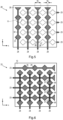
- a third touch panel 28 having an alternative arrangement of the first and second electrodes 23, 24 is shown.
- each first electrode 23 may include several first pad segments 29 evenly spaced in the first direction x and connected to one another in the first direction x by relatively narrower first bridging segments 30.
- each second electrode 24 may comprise several second pad segments 31 evenly spaced in the second direction y and connected to one another in the second direction y by relatively narrower second bridging segments 32.
- the first pad segments 29 are diamonds having a first width W 1 in the second direction y and the first bridging segments 30 have a second width W 2 in the second direction y.
- the second pad segments 31 and second bridging segments 32 of the second electrodes 24 have the same respective shapes and widths W 1 , W 2 as the first electrodes 23.
- the first electrodes 23 and the second electrodes 24 are arranged such that the second bridging segments 32 overlie the first bridging segments 30.
- the first electrodes 23 and the second electrodes 24 may be arranged such that the second pad segments 31 overlie the first pad segments 29.
- the pad segments 29, 31 need not be diamond shaped, and may instead be circular.
- the pad segments 29, 31 may take the form of a regular polygon such as a triangle, square, pentagon or hexagon.
- the pad segments 29, 31 may be I shaped or Z shaped.
- the first and second electrodes 23, 24 may take the form of interdigitated, comb-like, snowflake or Manhattan layouts.
- the second touch panel 21 may be exchanged for the third touch panel 28.
- the first and second electrodes 23, 24 are arranged on different, parallel planes within the touch panels 21, 28. However, in some examples the first and second electrodes 23, 24 may be disposed on substantially the same plane.
- a fourth touch panel 33 is shown.
- the fourth touch panel 33 is substantially the same as the third touch panel 28 except that the fourth touch panel 33 does not include the second layer structure 25 and the second electrodes 24 are disposed on the first face 13 of the first layer structure 12 in addition to the first electrodes 23.
- Each first electrode 23 is a continuous conductive region extending in the first direction x in the same way as the third touch panel 28.
- each first electrode 23 may include several first pad segments 34 evenly spaced in the first direction x and connected to one another in the first direction x by relatively narrower first bridging segments 35.
- Each second electrode 24 may comprise several second pad segments 36 evenly spaced in the second direction y in the same way as the third touch panel 28.
- the second pad segments 36 of the fourth touch panel 33 are disposed on the first face 13 of the first layer structure 12 and are interspersed with, and separated by, the first electrodes 23.
- the second pad segments 36 are connected together by conductive jumpers 37.
- the jumpers 37 each span a part of a first electrode 23 and the jumpers 37 are insulated from the first electrodes 23 by a thin layer of dielectric material (not shown) which may be localised to the area around the intersection of the jumper 37 and the first electrode 23.
- a thin dielectric layer may overlie the first face 13 of the first layer structure 12 and the first and second electrodes 23, 24.
- Conductive regions (not shown) extending in the second direction y may be disposed over the dielectric layer (not shown), each conductive region (not shown) overlying the second pad segments 36 making up one second electrode 24.
- the overlying conductive regions (not shown) may connect the second pad segments 36 making up each second electrode 24 using vias (not shown) formed through the dielectric layer (not shown).
- the second touch panel 21 may be exchanged for the fourth touch panel 33.
- the counter electrode 6 was disposed on, and substantially co-extensive with, the second surface 14 of the first layer structure 12.
- the counter electrode 6 may be replaced with one or more patterned counter electrodes.
- a fifth touch panel 38 is shown.
- Each sensing electrode 5, 23, 24 of the touch panel 38 takes the form of one or more sensing pads 40, 45 , and each sensing pad 40, 45 is opposed across the first layer structure 12 by a corresponding counter electrode pad 43a, 43b of a patterned counter electrode 39a, 39b.
- first electrodes 23 and a first patterned counter electrode 39a are shown.
- the first electrodes 23 and first patterned counter electrode 39a are disposed on the second surface 14 of a first layer structure 12.
- Each first electrode 23 includes several first sensing pads 40 evenly spaced in the first direction x and connected to one another in the first direction x by relatively narrower first bridging segments 41.
- the first patterned counter electrode 39a includes a number of first branches 42a.
- the first branches 42a each extend in the first direction x, and the first branches 42a are spaced apart in the second direction y and interdigitated with the first electrodes 23.
- the first branches 42a are all electrically connected together, for example, the first branches 42a may all connect to a single conductive trace 8 along one or more peripheral edges of the fifth touch panel 38.
- Each first branch 42a includes several first counter electrode pads 43a evenly spaced in the first direction x and connected to one another in the first direction x by relatively narrower first bridging counter electrode segments 44a.
- the second electrodes 24 and second patterned counter electrode 39b are disposed on the first surface 13 of the first layer structure 12.
- Each second electrode 24 includes several second sensing pads 45 evenly spaced in the second direction y and connected to one another in the second direction y by relatively narrower second bridging segments 46.
- the second patterned counter electrode 39b includes a number of second branches 42b.
- the second branches 42b each extend in the second direction y, and the second branches 42b are spaced apart in the first direction x and interdigitated with the second electrodes 24.
- the second branches 42b are all electrically connected together, for example, the second branches 42b may all connect to a single conductive trace 8 along one or more peripheral edges of the fifth touch panel 38.
- Each second branch 42b includes several second counter electrode pads 43b evenly spaced in the second direction y and connected to one another in the second direction y by relatively narrower second bridging counter electrode segments 44b.
- FIG. 9 a plan view of the fifth touch panel 38 is shown.
- the second electrodes 24 and the second patterned counter electrode 39b are arranged over the first electrodes 23 and the first patterned counter electrode 39a.
- the first layer structure 12 is not shown in Figure 9 to aid visualisation of the relative positioning of the electrodes 23, 24, 39a, 39b.
- Each first sensing pad 40 is opposed to a second counter electrode pad 43b across the first layer structure 12.
- each second sensing pad 45 is opposed to a first counter electrode pad 43a across the first layer structure 12.
- the fifth touch panel 38 may be optimised for location sensing using only piezoelectric signals 7, because the capacitance between sensing pads 40, 45 and corresponding counter electrode pads 43a, 43b may be maximised. This may increase the relative size of piezoelectric signals 7, compared to the second, third or fourth touch panels 21, 28, 33.
- the relative strength of piezoelectric signals 7 may be further increased by using a first layer structure 12 which only includes the layer of piezoelectric material 4.
- the sensing pads 40, 45 and the counter electrode pads 43a, 43b are diamond shaped in this example.
- the first sensing pads 40, 45 and counter electrode pads 43a, 43b may alternatively be square, circular, or any other regular or irregular shape.
- the sensing pads 40, 45 and the corresponding counter electrode pads 43a, 43b are the same shape.
- the counter electrode pads 43a, 43b have been drawn with slightly reduced areas compared to the sensing pads 40, 45 for the purposes of visualisation.
- each counter electrode pad 43a, 43b may have a shape and area matching the corresponding sensing pad 40, 45 in order to maximise collection of piezoelectric induced charges.
- the counter electrode pads 43a, 43b which will be closest to an input surface in use may be made relatively smaller in order to reduce the effects of screening of electrical fringing fields between the first and second electrodes 23, 24.
- the second touch panel 21 may be exchanged for the fifth touch panel 38.
- each branch 42a, 42b of the patterned counter electrodes need not all be connected to a single conductive trace 8. Instead, each branch 42a, 42b may be connected to the touch controller 3 using a separate conductive trace 8. In such a modification (not shown), instead of measuring applied forces 10 only from the sensing electrodes 5, applied forces 10 may additionally or alternatively be measured using the separately addressable patterned counter electrode branches 42a, 42b.
- the second electrodes 24 and branches 42b supported on the first face 13 may be connected to system ground or common mode (to provide electrostatic shielding), whilst applied forces 10 are measured using the first electrodes 23 and branches 42a supported on the second face 14.
- the first method is applicable to apparatuses 2, 22 which implement force and capacitance sensing, whether concurrently or sequentially.
- the first method may be used in combination with any touch panel 1, 21, 28, 33, 38, which may be used for measurements of force and capacitance.
- Measurements of applied force(s) 10 and capacitance values 20 are obtained by the touch controller (step S1).
- the apparatus 2, 22 measures force and capacitance concurrently, a single set of applied force(s) 10 and capacitance values 20 may be measured.
- the apparatus 2, 22 measures force and capacitance sequentially, one or more applied force(s) 10 may be measured, followed by measurements of the capacitance values 20, or vice versa.
- step S3 In response to receiving piezoelectric signals 7 (step S2, Yes), it is checked whether there are changes ⁇ C in the capacitance values 20 (step S3).
- the reception of piezoelectric signals 7 may correspond to piezoelectric signals 7 exceeding a pre-calibrated minimum piezoelectric signal threshold.
- checking whether piezoelectric signals 7 are received (step S2) may correspond to checking the time elapsed since piezoelectric signals 7 last exceeded the minimum piezoelectric signal.
- This condition checks for the application of a detectable force to the touch panel 1, 21, 28, 33, 38.
- Changes ⁇ C in the capacitance values 20 may correspond to differences between the capacitance values 20 and a set of baseline capacitance values which exceed minimum capacitance change thresholds.
- Minimum capacitance change thresholds may be determined upon start-up of the apparatus 2, 22, or may be pre-calibrated. This second condition checks for the presence of a conductive object close to, or touching, the touch panel 1, 21, 28, 33, 38.
- step S4 the touch controller 3 operates in a mixed force-capacitance mode.
- the touch controller 3 is configured to determine a location 9 corresponding to a user interaction 11 based on the determined changes ⁇ C in capacitance values 20 (step S5), and to determine an applied force 10 corresponding to the user interaction 11 based on the piezoelectric signals.
- the mixed force-capacitance mode (step S4) corresponds to a user interaction 11 which applies force to a touch panel 1, 21, 28, 33, 38 using a conductive object such as a user's digit or a conductive stylus.
- step S7 Whilst the first method continues (step S7, Yes), a further set of measurements is obtained (step S1).
- the touch controller 3 in response to in response to receiving piezoelectric signals (step S2, Yes) and determining no changes ⁇ C (at least no significant changes ⁇ C ) in capacitance values 20 for any of the sensing electrodes 5 (step S3, No), the touch controller 3 operates in a force-based mode (step S8).
- the touch controller 3 In the force-based mode (step S8), the touch controller 3 is configured to determine both a location 9 (step S9) and an applied force 10 (step S10) corresponding to a user interaction 11 based on the piezoelectric signals 7, without any input from capacitance values 20.
- the force-based mode (step S8) corresponds to a user interaction 11 which applies force to a touch panel 1, 21, 28, 33, 38 using a non-conductive object such as a user's gloved digit or a non-conductive stylus.
- the touch controller 2 In response to receiving no piezoelectric signals 7 (step S2, No), and also determining changes ⁇ C in capacitance values 20 of one or more sensing electrodes 5 (step S11, Yes), the touch controller 2 operated in a capacitance-based mode (step S12).
- the touch controller 3 In the capacitance based mode (step S12), the touch controller 3 is configured to determine a location 9 (step S13) corresponding to a user interaction 11 based on the determined changes ⁇ C in capacitance values 20.
- the capacitance-based mode (step S12) corresponds to a user interaction 11 which applies no or negligible force to a touch panel 1, 21, 28, 33, 38 using a conductive object such as a user's digit or a conductive stylus.
- step S1 In response to receiving no piezoelectric signals 7 (step S2, No), and also determining no changes ⁇ C in capacitance values 20 (step S11, No), there is no detectable user interaction 11 and the next set of measurements are obtained (step S1).
- the touch controller 3 may optimise signal processing for the conditions of ongoing user interactions 11.
- the processing of piezoelectric signals 7 may be optimised for maximum accuracy of determining applied force(s) 10. This may include aggregating piezoelectric signals 7 from one or more groups of sensing electrodes 5.
- the processing of the piezoelectric signals 7 may be optimised for accuracy in determining locations 9 of one or more user interactions 11, for example by treating piezoelectric signal 7 from each sensing electrode 5 separately.
- piezoelectric signals 7 may be ignored to save processing cycles/power.
- the touch controller 3 when the touch controller 3 operates in the mixed force-capacitance mode (step S4), the touch controller 3 may be configured to determine a location 9 corresponding to one or more user interactions 9 based on the determined changes ⁇ C in capacitance values 20, additionally augmented by the piezoelectric signals 7.
- the second method is the same as the first method, except that an additional check (step S14) is conducted before the touch controller 3 operates in mixed force-capacitance mode (step S4).
- the touch controller 3 in response to receiving piezoelectric signals 7 (step S2, Yes) and measuring changes ⁇ C in the capacitance values 20 (step S3, Yes), the touch controller 3 also checks whether the touch panel 1, 21, 28, 33, 38 is wet or submerged (step S14). The touch controller 3 may determine whether the touch panel 1, 21, 28, 33, 38 is wet or submerged based on the measured changes ⁇ C in the capacitance values 20. For example, when the touch panel 1, 21, 28, 33, 38 is wet or submerged, the fraction of sensing electrodes 5 registering changes ⁇ C and the magnitude of those changes ⁇ C may be inconsistent with even multiple user interactions 11. Appropriate thresholds may be determined based on calibration experiments conducted by applying progressively more droplets of water to the touch panel 1, 21, 28, 33, 38. Alternatively, measured changes ⁇ C in the capacitance values 20 corresponding to wet and dry touch panels 1, 21, 28, 33, 38 may be used to train a neural network based classifier.
- step S14 If the touch panel 1, 21, 28, 33, 38 is wet or submerged (step S14, Yes), the touch controller 3 operates in the force-based mode (step S8), despite the existence of measured changes ⁇ C in the capacitance values 20. If the touch panel 1, 21, 28, 33, 38 is not wet or submerged (step S14, No), the touch controller 3 operates in the mixed force-capacitance mode (step S4).
- a touch controller 3 carrying out the second method may avoid unreliable inputs when the touch panel 1, 21, 28, 33, 38 is wet or submerged by using the force-based mode to determine locations 9 of one or more user interactions 11 without relying on the measured changes ⁇ C in the capacitance values 20.
- the test for the touch panel 1, 21, 28, 33, 38 being wet or submerged may be expanded to encompass further criteria.
- the touch controller 3 may additionally or alternatively be configured to operate in the force-based mode (step S8) in response to determining that a signal-to-noise ratio for the capacitance values 20 is less than a pre-calibrated threshold.
- Such relatively high noise environments may be encountered in the in the presence of a high-frequency (10 kHz to 1 MHz) electrical noise environment, for example caused by proximity to a poorly shielded switched-mode power supply.
- the touch controller 3 may process received piezoelectric signals 7 differently in the force-based and mixed force-capacitance modes.
- the differences in processing may be differences in processing of digital signals, but may additionally or alternatively correspond to changes in one or more physical connections between the sensing electrodes 5 and the touch controller 3.
- the touch controller 3 may include a switch 47 ( Figure 13 ) configured so that:
- Each sensing electrode 5 remains coupled to a corresponding capacitance measurement channel 49 ( Figure 13 ) at all times.
- the sensing electrodes 5 may be coupled to the capacitance measurement channels 49 ( Figure 13 ) via high-pass filters, for example capacitances.
- piezoelectric signals 7 from individual sensing electrodes 5 may be processed individually in the force-based mode (step S8) to provide the best possible accuracy in determining locations 9 corresponding to user interactions 11.
- the piezoelectric signals 7 correspond to relatively low currents, and typically require amplification be a significant gain factor. High gain amplification may be relatively noisy and susceptible to interference from external electric fields.
- changes ⁇ C in capacitance values 20 are available for determining locations 9.
- piezoelectric signals 7 from two or more sensing electrodes 5 may be combined in order to increase the relatiove strength of the signal. Potentially, the amplification gain used may also be decreased.
- the first switching configuration includes a number, N, of sensing electrodes 5 1 , 5 2 , ..., 5 N which are connectable by a switch 47 to either a corresponding number N of piezoelectric signal sensing circuits 48 1 , 48 2 , ..., 48 N , or to a total piezoelectric signal sensing circuit 50.
- the switch 47 includes a number N of individual switch elements SW 1 , SW 2 , ..., SW N .
- the n th of N switch elements SW n may connect the corresponding n th sensing electrode 5 n to either the n th piezoelectric signal sensing circuit 48 n or to the total piezoelectric signal sensing circuit 50.
- each sensing electrode 5 1 , 5 2 , ..., 5 N The capacitive coupling of each sensing electrode 5 1 , 5 2 , ..., 5 N to a corresponding capacitance measurement channel 49 1 , 49 2 , ..., 49 N is shown in Figure 13 for reference, but is not drawn in Figure 14 as the capacitive coupling does not vary with the mode of the touch controller 3.
- the capacitance measurement channels 49 1 , 49 2 , ..., 49 N are not used in the force-based mode (step S8).
- the switch 47 when the touch controller 3 operates in the force-based mode (step S8), the switch 47 according to the first exemplary switching configuration connects each sensing electrode 5 n to the corresponding piezoelectric signal sensing circuit 48 n .
- the switch 47 when the touch controller 3 operates in the mixed force-capacitance mode (step S4), the switch 47 according to the first exemplary switching configuration connects all of the sensing electrodes 5 1 , 5 2 , ..., 5rr to the total piezoelectric signal sensing circuit 50.
- a significant resistance R in the range from about 10 k ⁇ to about 100 k ⁇ should also be provided in series between each capacitance measurement channel 49 1 , 49 2 , ..., 49 N and the corresponding switch elements SW 1 , SW 2 , ..., SW N .
- These resistances R may act to suppress or block high-frequency coupling of signals between capacitance measurement channels 49 1 , 49 2 , ..., 49 N via the switch elements SW 1 , SW 2 , ..., SW N .
- the corresponding switch element SW n may be temporarily opened to isolate the electrode 5 n for the duration of measuring a capacitance value 20.
- both a transmitting electrode 5 n and a receiving electrode 5 k may be temporarily isolated for the duration of the measurement using corresponding switch elements SW n , SW k .
- the second switching configuration includes a number, N, of sensing electrodes 5 1 , 5 2 , ..., 5 N which are connectable either individually or in pairs to a corresponding number N of piezoelectric signal sensing circuits 48 1 , 48 2 , ..., 48 N by a switch 47.
- the switch 47 includes a number N / 2 of individual switch elements SW 1,2 , SW 3,4 , ..., SW N-1,N .
- the switch element SW n-1,n may connect the n - 1 th and n th of N sensing electrodes 5n-1 , 5n to the corresponding piezoelectric signal sensing circuits 48 n-1 , 48 n , or the switch element SW n-1,n may connect both sensing electrodes 5 n-1 , 5 n to the n - 1 th piezoelectric signal sensing circuit 48 n-1 .
- the capacitive coupling of each sensing electrode 5 1 , 5 2 , ..., 5rr to a corresponding capacitance measurement channel 49 1 , 49 2 , ..., 49rr is not drawn in Figure 15 .
- the switch 47 is shown corresponding to the force-based mode (step S8) of the touch controller 3.
- the configuration of the switch elements SW 1,2 , SW 3,4 , ..., SW N-1,N corresponding to the mixed force-capacitance mode (step S4) is indicated in Figure 15 by dashed lines.
- touch panels 1, 21, 28, 33, 38 described hereinbefore have been illustrated with generally square shapes (square perimeters). However, touch panels 1, 21, 28, 33, 38 may have other shaped perimeters, for example rectangular, circular, elliptical, or any other regular or irregular perimeter shape.
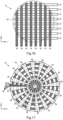
- FIG. 16 a sixth touch panel 51 is shown.
- the sixth touch panel 51 is the same as the second touch panel 21, except that the second touch panel 51 has a circular perimeter 52.
- the second layer structure 25 is not drawn in Figure 16 .
- the first and second sensing electrodes 23, 24 are truncated at one end by the circular perimeter 52 of the sixth touch panel 51.
- any hereinbefore described touch panel 1, 21, 28, 33, 38 may be modified to use a circular perimeter 52, or other shaped perimeter.
- Sensing electrodes 5 may be disposed according to any suitable coordinate system for determining locations 9 of user interactions 11 with the touch panel 1, 21, 28, 33, 38, 51.
- a seventh touch panel 53 is shown.
- the seventh touch panel 53 is the same as the second to fourth or sixth touch panels 21, 28, 33, 51, except that the first and second electrodes 23, 24 defining a Cartesian grid have been replaced with radial first electrodes 54 and circumferential second electrodes 55 defining a circular polar coordinate system ( ⁇ , r ).
- the radial first electrodes 54 measure the angle ⁇ of a location 9 with respect to the centre of the seventh touch panel 53
- the circumferential second electrodes 55 measure the radius r of a location 9 with respect to the centre of the seventh touch panel 53.
- the seventh touch panel 53 has a circular perimeter 52.
- the fifth touch panel 38 may be modified to employ radial first electrodes 54 and circumferential second electrodes 55.
- Apparatuses 2, 22 and touch panels 1, 21, 28, 33, 38, 51, 53 according to the present specification may be particularly advantageous when incorporated into a wearable device (not shown).
- apparatuses 2, 22 and touch panels 1, 21, 28, 33, 38, 51, 53 according to the present specification may operate underwater or when wetted by rain, wet fingers and so forth.
- a wearable device may take the form of a watch, a smart watch, a bracelet, a belt, a buckle, glasses, lenses of glasses, frames of glasses, jewellery, and so forth.
- the first and second methods of switching sensing modes may allow a wearable device to better handle varied input methods and/or challenging environmental conditions such as, for example, a wet or submerged touch panel 1, 21, 28, 33, 38, 51, 53, and so forth.
- a smart watch may incorporate a sixth or seventh touch panel 51, 53 and may include a touch controller 3 implementing the second method of switching sensing modes.
- sensing electrode 5 are disposed in regular patterns or arrays.
- the touch controller 3 and associated methods may also be used with touch panels in which sensing electrodes 5 are not disposed in regular patterns or arrays. Instead, the sensing electrodes 5 may be used to provide one or more discrete buttons for use on a control panel of a device.
- a button input panel 57 is shown.
- the button input panel 57 includes an outer layer 58 providing a user input surface 59, and stacked behind the outer layer 58 are sensing electrodes 5, a first layer structure 12, a counter electrode layer 6 and a light emitting diode (LED) layer 60.
- the button input panel 57 is a type of touch panel, and unless evidently incompatible, any description hereinbefore relating to touch panel(s) is equally applicable to the button input panel 57.
- FIG. 18 an example of a user input surface 59 is shown.
- the user input surface 59 shown in Figure 18 is for a washing machine (not shown), although the button input panel 57 may be readily adapted and applied to any device or machinery which requires or receives user input.
- Graphics, text or other indicia are printed or otherwise applied to the user input surface 59 (or the other side of the outer layer 58 if transparent) to define regions where a user may interact with the button input panel 57.
- a "Program" input area 61 is defined, including text corresponding to the different types of washing cycles which the washing machine can run. Each section of text is positioned over a corresponding sensing electrode 5 in the form of a first button electrode 62 belonging to a first group of buttons 63.
- a "Temp” input area 64 is defined, containing text corresponding to different wash temperatures and overlying sensing electrodes 5 in the form of second button electrodes 65 belonging to a second group of buttons 66.
- a "Spin” input area 67 is defined, containing text corresponding to different spin speeds and overlying sensing electrodes 5 in the form of third button electrodes 68 belonging to a third group of buttons 69.
- a power button electrode 70 is overlaid by a suitable graphic, as are a start button electrode 71 and a pause button electrode 72.
- the user input surface 59 may be generally opaque except for a transparent window 73 which is provided for viewing an underlying display 74.
- the display 74 may be provided as part of the LED layer 60, for example using one or more organic light emitting diodes (OLEDs), or the display 74 may be a separate device mounted to the underside of the button input panel 57, for example a liquid crystal display or OLED display.
- OLEDs organic light emitting diodes
- the area corresponding to each button electrode 62, 65, 68, 70, 71, 72 is at least partially translucent to allow particular buttons to be individually illuminable using the LED layer 60.
- buttons electrodes 65, 68, 70, 71, 72 can be visually indicated, for example, if the currently selected temperature is 60°C, then the second button electrode 65 underlying the text "60°C" may be illuminated whilst all the other buttons electrodes 65 of the second group 66 are not illuminated.
- the outer layer 58 may be transparent, and areas other than the transparent window 73 may be printed (for example on the opposite side to the user input surface) using opaque ink. Text or other indicia overlying button electrodes 62, 65, 68, 70, 71, 72 may be defined by omitting the opaque ink, or by using a different, translucent ink.
- each of the button electrodes 62, 65, 68, 70, 71, 72 is connected to the touch controller 3 via a corresponding conductive trace 8.
- the operation of the touch controller 3 is the same as described hereinbefore.
- the touch controller 3 measures forces 10 applied to the button electrodes 62, 65, 68, 70, 71, 72, locations 9 in the form of the identities of any actuated button electrodes 62, 65, 68, 70, 71, 72, and optionally self-capacitances of the button electrodes 62, 65, 68, 70, 71, 72.
- the button input panel 57 has a similar structure to the first touch panel 1, except that the cover lens 17 is replaced by the outer layer 58, the display 16 is replaced by the LED layer 60 and the sensing electrodes 5 have a different pattern.
- the LED layer 60 includes a light emitting diode (LED) 75 arranged to underlie each of the button electrodes 62, 65, 68, 70, 71, 72 in order to provide illumination indicative of actuating the button electrodes 62, 65, 68, 70, 71, 72.
- LED light emitting diode
- the intervening layers of counter electrode 6, first layer structure 12, button electrodes 62, 65, 68, 70, 71, 72 and pressure sensitive adhesive 18 should be transparent or at least translucent.
- the LED layer 60 may be omitted.
- a backlight (not shown) may be combined with a liquid crystal array (not shown) to provide selective illumination of the button electrodes 62, 65, 68, 70, 71, 72, and optionally the display 74.
- Each LED 75 may single or multi-coloured.
- feedback of force values 10 from the touch controller 3 may be used to alter the colour emitted to illuminate a corresponding button electrode 62, 65, 68, 70, 71, 72 in dependence on the magnitude of a corresponding applied force 10.
- the button input panel 57 may employ any of the hereinbefore described methods of switching input modes between capacitance-based, force-based and mixed force-capacitance modes. This may be advantageous in the context of a washing machine, as a user's hands may often be wet, and the ambient environment may often be humid and prone to condensation (e.g. from a tumble dryer machine). In this environment, replacement of mechanical buttons with capacitive buttons alone may not be practical.
- the devices and methods of the present specification may be used in this environment because even if a user's hands are wet and/or a thin film of condensed water vapour has formed over the user input surface, the force sensing mode may still reliably detect user input.
- a counter electrode layer may be patterned to correspond to the button electrodes 62, 65, 68, 70, 71, 72, for example the second face 14 may be patterned with a number of patterned counter electrodes having an identical layout to that shown in Figure 19 .
- patterned counter electrodes identical layout to Figure 19
- they may all be connected together so that forces may be measured between any button electrode 62, 65, 68, 70, 71, 72 and the patterned counter electrodes (identical layout to Figure 19 ).
- each patterned counter electrode may be connected to a separate conductive trace 8, enabling differential force measurements to be obtained for each individual button electrode 62, 65, 68, 70, 71, 72.
- the touch controller 3 may measure applied forces 10 using the patterned counter electrodes (identical layout to Figure 19 ), whilst connecting the corresponding button electrodes 62, 65, 68, 70, 71, 72 to system ground or common mode voltage to provide electrostatic shielding.
- Counter electrode measurement of force values 10 may be performed in the force-based mode, and/or time multiplexed with capacitance measurements in the mixed force-capacitance
- a counter electrode layer may include separate electrodes (not shown) corresponding to each of the power, start and pause button electrodes 70, 71, 72, and further electrodes (not shown) each of which is coextensive with one of the first, second and third groups 63, 66, 69 of electrodes.
- This latter approach represents a hybrid approach in which some button electrodes 70, 71, 72 are opposed by a matching counter electrodes (not shown), whereas each group 63, 66, 69 of electrodes is opposed by a common counter electrode (not shown).
- Counter electrode 6 measurements of applied force 10 would be possible using such a hybrid approach.
- the touch controller 3 may be configured to cycle through the options each time the common counter electrode (not shown) is actuated.
- the currently selected option may be indicated by illumination from the LED layer 60.
- the display 74 of the button input panel 57 is optional, and in other example may be omitted.
- the button input panel 57 is not limited to a washing machine, and with suitable customisation of the number and shape of button electrodes 62, 65, 68, 70, 71, 72 and overlying indicia, may be used in conjunction with any device requiring or receiving user input.
- suitable uses include kitchen or other domestic appliances, in-car button controls and/or infotainment screens mounted to a car dashboard, industrial equipment interfaces, medical equipment interfaces, ruggedised outdoor tablets, laptops, point-of-sale units and so forth, parking ticket machine interfaces, outdoor wearable use (e.g. fitness watches), marine equipment interfaces, and so forth.
- These applications all have in common that a user may be wearing protective gloves (e.g. protective gloves in an industrial setting, latex/nitrile gloves in a clinical setting) which may interfere with capacitive sensing, and/or an input panel may become wet or fully/partially submerged.
Landscapes
- Engineering & Computer Science (AREA)
- General Engineering & Computer Science (AREA)
- Theoretical Computer Science (AREA)
- Human Computer Interaction (AREA)
- Physics & Mathematics (AREA)
- General Physics & Mathematics (AREA)
- Computer Networks & Wireless Communication (AREA)
- Position Input By Displaying (AREA)
- User Interface Of Digital Computer (AREA)
Description
- The present invention relates to a touch panel for force sensing.
- Resistive and capacitive touch panels are used as input devices for computers and mobile devices. One type of capacitive touch panel, projected capacitance touch panels, is often used for mobile devices because an exterior layer may be made of glass, providing a hard surface which is resistant to scratching. An example of a projected capacitance touch panel is described in
US 2010/0079384 A1 . - Touch panels which use piezoelectric based force-detection have been proposed. For example
JP 2010-026938 A - Examples of touch sensors combining capacitive sensing with piezoelectric based force-detection capabilities are described in
WO 2016/102975 A1 . Further examples of touch sensors combining capacitive sensing with piezoelectric based force-detection capabilities are described inWO 2017/109455 A1 ,WO 2019/030513 A1 andUS 2017/262099 A1 . -
US2018/0059866 A1 discloses a touch panel using capacitive touch and force detection to discriminate between intended touches, including when the user is wearing gloves, and unintended touches or contamination of the touch panel caused by water. -
US2018/0341347 A1 discloses a touch panel using acoustic touch and force detection that can detect touches even when the panel is wet or submerged. - According to a first aspect of the invention, there is provided apparatus which includes a touch panel. The touch panel includes a layer of piezoelectric material disposed between a number of sensing electrodes and at least one counter electrode. The apparatus also includes a touch controller connected to the touch panel. The touch controller is configured to determine, in response to receiving piezoelectric signals from one or more of the sensing electrodes, a location and an applied force corresponding to a user interaction with the touch panel. The touch controller is configured, in response to receiving piezoelectric signals and determining no changes in the capacitance values for any of the sensing electrodes, to operate in a force-based mode wherein the touch controller is configured to determine a location and an applied force corresponding to a user interaction based on the piezoelectric signals. The touch controller is configured, in response to determining changes in the capacitance values of one or more sensing electrodes and receiving no piezoelectric signals, to operate in a capacitance-based mode wherein the touch controller is configured to determine a location corresponding to a user interaction based on the determined changes in capacitance values. The touch controller is configured, in response to determining changes in the capacitance values of one or more sensing electrodes and receiving piezoelectric signals, to operate in a mixed force-capacitance mode wherein the touch controller is configured to determine a location corresponding to a user interaction based on the determined changes in capacitance values and to determine an applied force corresponding to the user interaction based on the piezoelectric signals.
- Each sensing electrode may include one or more sensing pads. Each sensing pad may be opposed across the layer of piezoelectric material by a corresponding counter electrode pad of a counter electrode.
- The touch controller may also be configured to determine a capacitance value of one or more of the sensing electrodes.
- The touch controller may be configured to determine one or more capacitance values and to receive one or more piezoelectric signals concurrently.
- The touch controller may be configured to determine one or more capacitance values and to receive one or more piezoelectric signals sequentially.
- In the mixed force-capacitance mode, the touch controller may be configured to determine a location corresponding to a user interaction based on the determined changes in the capacitance values and the piezoelectric signals.
- The touch controller may also be configured to determine whether the touch panel is wet or submerged based on the determined capacitance values of the sensing electrodes. The touch controller may also be configured, in response to determining that the touch panel is wet, to operate in the force-based mode.
- The touch controller may also be configured to operate in the force-based mode in response to determining that a signal-to-noise ratio of the capacitance values is less than a pre-calibrated threshold.
- The apparatus may also include a switch configured such that when the touch controller operates in the force-based mode, the switch connects each sensing electrode to a corresponding piezoelectric signal sensing circuit. The switch may be configured such that when the touch controller operates in the mixed force-capacitance mode, the switch connects two or more sensing electrodes to one piezoelectric signal sensing circuit.
- The sensing electrodes may include a number of first electrodes and a number of second electrodes. Each first electrode may extend in a first direction, and the first electrodes may be spaced apart in a second direction which is perpendicular to the first direction. Each second electrode may extend in the second direction, and the plurality of second electrodes may be spaced apart in the first direction.
- The first and second electrodes may be arranged on the same plane within the touch panel.
- The first and second electrodes may be arranged on different, parallel planes within the touch panel.
- The touch panel may have a circular or elliptical perimeter. The touch panel may have a square or rectangular perimeter.
- The touch panel may be a button input panel. A button input panel may include one or more sensing electrodes in the form of discrete button electrodes. Button electrodes of the button input panel may have different sizes and/or shapes. The counter electrode of the button input panel may be uniform. The counter electrode of the button input panel may be patterned to match the shapes and positions of the button electrodes. Patterned counter electrodes may all be electrically connected to one another. Patterned counter electrodes may be connected to individual conductive traces to enable patterned counter electrodes to be addressed individually. The button input panel may include a light emitting diode layer including one or more light emitting diodes. Each light emitting diode may be disposed and configured to illuminate a corresponding button electrode.
- A wearable device may include the apparatus. A wearable device may take the form of a watch, a smart watch, a bracelet, a belt, a buckle, glasses, lenses of glasses, frames of glasses, jewellery, and so forth.
- According to a second aspect of the invention there is provided a method for processing signals from a touch panel. The touch panel includes a layer of piezoelectric material disposed between a plurality of sensing electrodes and at least one counter electrode. The method includes, in response to receiving piezoelectric signals from one or more of the sensing electrodes, determining a location corresponding to a user interaction with the touch panel based on the piezoelectric signals. The method also includes determining a capacitance value of one or more of the sensing electrodes. The method also includes, in response to receiving piezoelectric signals and determining no changes in the capacitance values for any of the sensing electrodes, determining, in a force-based mode, a location and an applied force corresponding to a user interaction based on the piezoelectric signals. The method also includes, in response to determining changes in the capacitance values of one or more sensing electrodes and receiving no piezoelectric signals, determining, in a capacitance-based mode, a location corresponding to a user interaction based on the determined changes in capacitance values. The method also includes, in response to determining changes in the capacitance values of one or more sensing electrodes and receiving piezoelectric signals, determining, in a mixed force-capacitance mode, a location corresponding to a user interaction based on the determined changes in capacitance values and determining an applied force corresponding to the user interaction based on the piezoelectric signals.
- Determining capacitance values of one or more of the sensing electrodes may be performed concurrently with receiving piezoelectric signals from one or more of the sensing electrodes.
- Determining capacitance values of one or more of the sensing electrodes may be performed sequentially with receiving piezoelectric signals from one or more of the sensing electrodes. Sequentially may include alternating between determining capacitance values and receiving piezoelectric signals.
- In the mixed force-capacitance mode, the location corresponding to a user interaction may be determined based on the determined changes in capacitance values and the piezoelectric signals.
- The method may also include determining whether the touch panel is wet or submerged based on the determined capacitance values of the sensing electrodes. The method may also include, in response to determining that the touch panel is wet, operating in the force-based mode.
- The method may also include operating in the force-based mode in response to determining that a signal-to-noise ratio of the capacitance values is less than a pre-calibrated threshold.
- The touch panel may be a button input panel. A button input panel may include one or more sensing electrodes in the form of discrete button electrodes. Button electrodes of the button input panel may have different sizes and/or shapes. The counter electrode of the button input panel may be uniform. The counter electrode of the button input panel may be patterned to match the shapes and positions of the button electrodes. Patterned counter electrodes may all be electrically connected to one another. Patterned counter electrodes may be connected to individual conductive traces to enable patterned counter electrodes to be addressed individually. The button input panel may include a light emitting diode layer including one or more light emitting diodes. Each light emitting diode may be disposed and configured to illuminate a corresponding button electrode.
- Certain embodiments of the present invention will now be described, by way of example, with reference to the accompanying drawings in which:
-
Figure 1 is a schematic cross-section of a first touch panel; -
Figure 2 schematically illustrates a first apparatus; -
Figure 3 is a schematic cross-section of a second touch panel; -
Figure 4 schematically illustrates a second apparatus; -
Figure 5 is a schematic plan-view of a third touch panel; -
Figure 6 is a schematic plan-view of a fourth touch panel; -
Figure 7 is a schematic plan-view of first electrodes and a first patterned counter electrode for a fifth touch panel; -
Figure 8 is a schematic plan-view of second electrodes and a second patterned counter electrode for the fifth touch panel; -
Figure 9 is a schematic plan-view of the fifth touch panel; -
Figure 10 is a schematic cross-section of the fifth touch panel; -
Figure 11 is a process flow diagram of a first method of switching sensing modes; -
Figure 12 is a process flow diagram of a second method of switching sensing modes; -
Figures 13 and 14 illustrate a first exemplary switching configuration; -
Figure 15 illustrates a second exemplary switching configuration; -
Figure 16 is a schematic plan-view of a sixth touch panel; -
Figure 17 is a schematic plan-view of a seventh touch panel; -
Figure 18 is a schematic plan-view of a user input surface of a button input panel; -
Figure 19 schematically illustrates connections between sensing electrodes of the button input panel shown inFigure 18 and a touch controller; and -
Figure 20 is a schematic cross-section along the line labelled B-B' inFigure 19 . - In the following description, like parts are denoted by like reference numerals.
- Projected capacitance touch panels operate by detecting changes in electric fields caused by the proximity of a conductive object. However, when a projected capacitance screen is wet, or fully submerged, the presence of water may cause the determination of a number of and locations of user touches based on capacitance values to become unreliable or entirely non-functional.
- Touch panels which operate using combined force sensing and capacitance sensing may use the capacitance measurements to determine the locations of one or more touches. However, such measurements suffer the same issues as a pure capacitive touch panel when wet or submerged underwater. Furthermore, capacitance measurements will not detect a user touch using a non-conductive object, or through most conventional gloves.
- The present specification concerns apparatuses and methods which may mitigate one or more of these issues.
- Referring to
Figure 1 , a schematic cross section of a display stack-up including afirst touch panel 1 is shown. - Referring also to
Figure 2 , afirst apparatus 2 is shown. - The
first apparatus 2 includes thefirst touch panel 1 and atouch controller 3. In general, thetouch panel 1 includes a layer ofpiezoelectric material 4 disposed between a number ofsensing electrodes 5 and at least onecounter electrode 6. Thetouch controller 3 is electrically connected to thesensing electrodes 5 of thetouch panel 1. Thetouch controller 3 is configured to receivepiezoelectric signals 7 from one or more of thesensing electrodes 5 via corresponding conductive traces 8. In dependence on the receivedpiezoelectric signals 7, thetouch controller 3 is configured to determine alocation 9 and an appliedforce 10 corresponding to auser interaction 11 with thetouch panel 1. Thetouch controller 3 may be configured to amplify and/or filter the piezoelectric signals 7. Thetouch controller 3 may determine alocation 9 and an appliedforce 10 by interpolating values of thepiezoelectric signals 7 to determine an implied position and magnitude of a peak piezoelectric signal, which may correspond to alocation 9 between a pair ofsensing electrodes 5. The implied magnitude of a peakpiezoelectric signal 7 may be mapped to an applied force using calibration data, and the mapping may depend on thelocation 9 of theuser interaction 11. Thetouch controller 3 may be configured to determinelocations 9 and appliedforces 10 corresponding to two or more simultaneous (or concurrent)user interactions 11. - By determining
locations 9 using only an applied force, thefirst apparatus 2 may continue to function without interruption even when thetouch panel 1 is wet or submerged. Additionally or alternatively, thefirst apparatus 2 may continue to function even in environments which experience a relatively high level of electromagnetic interference. Such functionality may be particularly advantageous for wearable devices such as smart watches, which are more likely to be worn when swimming, or to become wet from, for example, rain, wet fingers, sweat and so forth. Although smart watches and other devices may be made waterproof, there has been little incentive to use them in wet environments such as, for example, a swimming pool, because a conventional projected capacitance touch panel does not function when wet or submerged. - The
first touch panel 1 includes, stacked in a thickness direction z, thecounter electrode 6, afirst layer structure 12 which includes the layer ofpiezoelectric material 4, and thesensing electrodes 5. Thefirst layer structure 12 has afirst face 13 and a second, opposite, face 14. Thefirst layer structure 12 includes one or more layers, including at least the layer ofpiezoelectric material 4. Each layer included in thefirst layer structure 12 is generally planar and extends in first x and second y directions which are perpendicular to a thickness direction z. The one or more layers of thefirst layer structure 12 are arranged between the first and second faces 13, 14 such that the thickness direction z of each layer of thefirst layer structure 12 is perpendicular to the first and second faces 13, 14. - The
sensing electrodes 5 are disposed on thefirst face 13 of thefirst layer structure 12, and thecounter electrode 6 is disposed on thesecond face 14 of thefirst layer structure 12. Eachsensing electrode 5 takes the form of a conductive pad 15. The conductive pads 15 are disposed on thefirst face 13 in an array extending in the first and second directions x, y. Eachsensing electrode 5 in the form of a conductive pad 15 is coupled to a corresponding input of thetouch controller 3 by a respectiveconductive trace 8. Thecounter electrode 6 is disposed on thesecond face 14 and is extensive such that thecounter electrode 6 at least partial underlies eachsensing electrode 5 in the form of a conductive pad 15. Thecounter electrode 6 may be substantially coextensive with thesecond face 14. Thecounter electrode 6 is coupled to a common mode voltage Vcm , system ground and/or to thetouch controller 3 via a return path (not shown). - The
first touch panel 1 may be bonded overlying thedisplay 16 of an electronic device such as, for example, a mobile phone, a tablet computer, a laptop computer, a smart watch or other wearable device, and so forth. In such contexts, the materials of thefirst touch panel 1 should be substantially transparent. Acover lens 17 is typically bonded overlying thefirst touch panel 1. Thecover lens 17 is preferably glass but may be any transparent material including transparent polymers. Thecover lens 17 may be bonded to thefirst touch panel 1 using a layer of pressure sensitive adhesive (PSA)material 18. The layer ofPSA material 18 may also be substantially transparent. The array ofsensing electrodes 5 and the correspondingconductive traces 8 may be fabricated using index matching techniques to minimise visibility to a user. - The layer of
piezoelectric material 4 is a piezoelectric polymer such as polyvinylidene fluoride (PVDF) or or polylactic acid (PLLA). However, the layer ofpiezoelectric material 4 may alternatively be a layer of a piezoelectric ceramic such as lead zirconate titanate (PZT). Thesensing electrodes 5 andcounter electrode 6 may be formed from indium tin oxide (ITO) or indium zinc oxide (IZO). Thesensing electrodes 5 andcounter electrode 6 may be formed from metal films such as aluminium, copper, silver or other metals suitable for deposition and patterning as a thin film. Thesensing electrodes 5 andcounter electrode 6 may be formed from conductive polymers such as polyaniline, polythiphene, polypyrrole or poly(3,4-ethylenedioxythiophene) polystyrene sulfonate (PEDOT/PSS). Thesensing electrodes 5 andcounter electrode 6 may be formed from a metal mesh; nanowires, for example silver nanowires; graphene; and/or carbon nanotubes. - The
first layer structure 12 may include only the layer ofpiezoelectric material 4, such that the first and second opposite faces 13, 14 are faces of the layer ofpiezoelectric material 4. Alternatively, thefirst layer structure 12 may include one or more dielectric layers 19 (Figure 3 ) stacked between the layer ofpiezoelectric material 4 and thefirst face 13 of thefirst layer structure 12. Thefirst layer structure 12 may include one or more dielectric layers 19 (Figure 3 ) stacked between thesecond face 14 of thefirst layer structure 12 and the layer ofpiezoelectric material 4. One or more dielectric layer(s) 19 (Figure 3 ) may include layers of a polymer dielectric material such as polyethylene terephthalate (PET), or layers of pressure sensitive adhesive (PSA) material. However, one or more dielectric layer(s) 19 (Figure 3 ) may include layers of a ceramic insulating material such as aluminium oxide. - The conductive traces 8 may be made of the same material as the
sensing electrodes 5. Alternatively, theconductive traces 8 may be made of a material having a higher conductivity than the material used for thesensing electrodes 5. The conductive traces 8 are generally much thinner in the plane defined by the first and second directions x, y than the correspondingsensing electrodes 5. - In the example of the
first touch panel 1 shown inFigures 1 and 2 , the first and second faces 13, 14 and the layers of thefirst layer structure 12 are shown extending along orthogonal axes labelled x and y, and the thickness direction of each layer of thefirst layer structure 12 is aligned with an axis labelled z which is orthogonal to the x and y axes. However, the first, second and thickness directions need not form a right handed orthogonal set as shown. For example, the first and second directions x, y may intersect at an angle of 30 degrees or 45 degrees or any other angle greater than 0 degrees and less than 90 degrees. - The
touch controller 3 is further configured to determine one ormore capacitance values 20, eachcapacitance value 20 corresponding to one, or a pairing, of thesensing electrodes 5. Thetouch controller 3 may determine acapacitance value 20 corresponding to eachsensing electrode 5 and/or each pairing ofsensing electrodes 5. - The
touch controller 3 may receive and measurepiezoelectric signals 7 andcapacitance values 20 concurrently. For example, as described inWO 2017/109455 A1 , or as described inWO 2016/102975 A2 . In particular, see the combined force and capacitance touch panel systems shown in, and described with reference to,Figures 15 to 20 ofWO 2016/102975 A2 . Further, suitable combined force and capacitance touch panel systems are shown in, and described with reference to, Figures 22 and 23 ofWO 2017/109455 A1 . - Alternatively, the
touch controller 3 may receive and measurepiezoelectric signals 7 andcapacitance values 20 sequentially, for example, as described inWO 2014/005218 A1 . In particular, see the combined force and capacitance touch panel systems shown in, and described with reference to,Figures 4 to 6 ofWO 2014/005218 . - Referring to
Figure 3 , a schematic cross section of asecond touch panel 21 is shown. - Referring also to
Figure 4 , asecond apparatus 22 is shown. - The
second apparatus 22 includes thesecond touch panel 21 and thetouch controller 3. Thetouch controller 3 is substantially the same as for thefirst apparatus 2. - Compared to the
first touch panel 1, thesensing electrodes 5 of thesecond touch panel 21 are divided intofirst electrodes 23 andsecond electrodes 24. Additionally, thesecond touch panel 21 also includes asecond layer structure 25. Stacked in the thickness direction, thesecond touch panel 21 includes thecounter electrode 6, thefirst layer structure 12, thesensing electrodes 5 in the form offirst electrodes 23, thesecond layer structure 25 and thesensing electrodes 5 in the form ofsecond electrodes 24. - The
second layer structure 25 has athird face 26 and a fourth, opposite, face 27. Thesecond layer structure 25 includes one or more dielectric layers 19. Eachdielectric layer 19 is generally planar and extends in first x and second y directions which are perpendicular to a thickness direction z. The one or moredielectric layers 19 of thesecond layer structure 25 are arranged between the third and fourth faces 26, 27 such that the thickness direction z of eachdielectric layer 18 of thesecond layer structure 25 is perpendicular to the third and fourth faces 26, 27. - The
first electrodes 23 each extend in the first direction x and thefirst electrodes 23 are disposed in an array evenly spaced in the second direction y. Thesecond electrodes 24 each extend in the second direction y and thesecond electrodes 24 are disposed in an array evenly spaced in the first direction x. Eachfirst electrode 23 and eachsecond electrode 24 are coupled to a corresponding input of thetouch controller 3 by a respectiveconductive trace 8. Thefirst electrodes 23 may be disposed on thefirst surface 13 of thefirst layer structure 12, or on thefourth surface 27 of thesecond layer structure 25. Thesecond electrodes 24 may be disposed on thethird surface 26 of thesecond layer structure 25, or on the underside of acover lens 17 bonded over thesecond touch panel 21. Thecounter electrode 6 is disposed on thesecond face 14 and is extensive such that thecounter electrode 6 at least partially underlies eachfirst electrode 23 and eachsecond electrode 24. Thecounter electrode 6 may be substantially coextensive with thesecond face 14. Thecounter electrode 6 is coupled to a common mode voltage Vcm , system ground and/or thetouch controller 3. - The
touch controller 3 may address eachsensing electrode second electrodes touch controller 3 to determinelocations 9 and appliedforces 10 corresponding to one ormore user interactions 11. - By determining
locations 9 using only an applied force, the first apparatus may continue to function without interruption even when thesecond touch panel 21 is wet or submerged. Additionally or alternatively, thefirst apparatus 2 may continue to function even in environments which experience a relatively high level of electromagnetic interference. Such functionality may be particularly advantageous for wearable devices such as smart watches, which are more likely to be worn when swimming, or to become wet from, for example, rain, wet fingers, sweat and so forth. Although smart watches and other devices may be made waterproof, there has been little incentive to use them in wet environments such as, for example, a swimming pool, because a conventional projected capacitance touch panel does not function when wet or submerged. - The dielectric layer(s) 19 may include layers of a polymer dielectric material such as PET or layers of PSA materials. However, the dielectric layer(s) 19 may include layers of a ceramic insulating material such as aluminium oxide.
- The
second layer structure 25 may include only asingle dielectric layer 19, such that the third and fourth opposite faces 26, 27 are faces of asingle dielectric layer 19. Alternatively, asecond layer structure 25 need not be used, and thesecond electrodes 24 may be disposed on thefirst face 13 along with the first electrodes 23 (Figure 6 ). - In
Figures 3 and 4 , the third and fourth faces 26, 27 and thedielectric layers 19 of thesecond layer structure 25 are shown extending along orthogonal axes labelled x and y, and the thickness direction of eachdielectric layer 19 of thesecond layer structure 25 is aligned with an axis labelled z which is orthogonal to the x and y axes. However, the first, second and thickness directions x, y, z need not form a right handed orthogonal set as shown. - In the same way as the
first apparatus 2, thetouch controller 3 of thesecond apparatus 22 may also determine capacitance values 20. For thefirst apparatus 2, the capacitance values 20 measured by thetouch controller 3 correspond to self-capacitances of the conductive pads 15. For thesecond apparatus 22, the capacitance values 20 measured by thetouch controller 3 may correspond to self-capacitances of the first andsecond electrodes first electrode 23 and asecond electrode 24. - The
touch controller 3 may receive and measurepiezoelectric signals 7 andcapacitance values 20 concurrently. For example, as described inWO 2017/109455 A1 , or as described inWO 2016/102975 A2 . In particular, see the combined force and capacitance touch panel systems shown in, and described with reference to, Figures 21 to 26 ofWO 2016/102975 A2 . Further, suitable combined force and capacitance touch panel systems are shown in, and described with reference to,Figures 4 to 21 ofWO 2017/109455 A1 . - Alternatively, the
touch controller 3 may receive and measurepiezoelectric signals 7 andcapacitance values 20 sequentially, for example, as described inWO 2014/005218 A1 . In particular, see the combined force and capacitance touch panel systems shown in, and described with reference to,Figures 5 to 8 ofWO 2014/005218 . - The
second touch panel 21 may be bonded overlying thedisplay 16 of an electronic device and acover lens 17 may be bonded overlying thesecond touch panel 21 in the same way as for thefirst touch panel 1. - Although the first and
second electrodes - For example, referring also to
Figure 5 , athird touch panel 28 having an alternative arrangement of the first andsecond electrodes - Instead of being rectangular, each
first electrode 23 may include severalfirst pad segments 29 evenly spaced in the first direction x and connected to one another in the first direction x by relatively narrowerfirst bridging segments 30. Similarly eachsecond electrode 24 may comprise severalsecond pad segments 31 evenly spaced in the second direction y and connected to one another in the second direction y by relatively narrowersecond bridging segments 32. Thefirst pad segments 29 are diamonds having a first width W1 in the second direction y and thefirst bridging segments 30 have a second width W2 in the second direction y. Thesecond pad segments 31 andsecond bridging segments 32 of thesecond electrodes 24 have the same respective shapes and widths W1 , W2 as thefirst electrodes 23. - The
first electrodes 23 and thesecond electrodes 24 are arranged such that thesecond bridging segments 32 overlie thefirst bridging segments 30. Alternatively, thefirst electrodes 23 and thesecond electrodes 24 may be arranged such that thesecond pad segments 31 overlie thefirst pad segments 29. Thepad segments pad segments pad segments second electrodes - In the
second apparatus 22, thesecond touch panel 21 may be exchanged for thethird touch panel 28. - In the second and
third touch panels second electrodes touch panels second electrodes - For example, referring also to
Figure 6 , afourth touch panel 33 is shown. - The
fourth touch panel 33 is substantially the same as thethird touch panel 28 except that thefourth touch panel 33 does not include thesecond layer structure 25 and thesecond electrodes 24 are disposed on thefirst face 13 of thefirst layer structure 12 in addition to thefirst electrodes 23. Eachfirst electrode 23 is a continuous conductive region extending in the first direction x in the same way as thethird touch panel 28. For example, eachfirst electrode 23 may include severalfirst pad segments 34 evenly spaced in the first direction x and connected to one another in the first direction x by relatively narrowerfirst bridging segments 35. Eachsecond electrode 24 may comprise severalsecond pad segments 36 evenly spaced in the second direction y in the same way as thethird touch panel 28. However, unlike thethird touch panel 28, thesecond pad segments 36 of thefourth touch panel 33 are disposed on thefirst face 13 of thefirst layer structure 12 and are interspersed with, and separated by, thefirst electrodes 23. Thesecond pad segments 36 are connected together byconductive jumpers 37. Thejumpers 37 each span a part of afirst electrode 23 and thejumpers 37 are insulated from thefirst electrodes 23 by a thin layer of dielectric material (not shown) which may be localised to the area around the intersection of thejumper 37 and thefirst electrode 23. - Alternatively, a thin dielectric layer (not shown) may overlie the
first face 13 of thefirst layer structure 12 and the first andsecond electrodes second pad segments 36 making up onesecond electrode 24. The overlying conductive regions (not shown) may connect thesecond pad segments 36 making up eachsecond electrode 24 using vias (not shown) formed through the dielectric layer (not shown). - In the second apparatus, the
second touch panel 21 may be exchanged for thefourth touch panel 33. - In the first to
fourth touch panels counter electrode 6 was disposed on, and substantially co-extensive with, thesecond surface 14 of thefirst layer structure 12. However, in some examples thecounter electrode 6 may be replaced with one or more patterned counter electrodes. - For example, referring also to
Figures 7 to 10 , afifth touch panel 38 is shown. - Each
sensing electrode touch panel 38 takes the form of one ormore sensing pads sensing pad first layer structure 12 by a correspondingcounter electrode pad counter electrode - Referring in particular to
Figure 7 , an arrangement offirst electrodes 23 and a firstpatterned counter electrode 39a is shown. - The
first electrodes 23 and firstpatterned counter electrode 39a are disposed on thesecond surface 14 of afirst layer structure 12. Eachfirst electrode 23 includes severalfirst sensing pads 40 evenly spaced in the first direction x and connected to one another in the first direction x by relatively narrowerfirst bridging segments 41. The firstpatterned counter electrode 39a includes a number offirst branches 42a. Thefirst branches 42a each extend in the first direction x, and thefirst branches 42a are spaced apart in the second direction y and interdigitated with thefirst electrodes 23. Thefirst branches 42a are all electrically connected together, for example, thefirst branches 42a may all connect to a singleconductive trace 8 along one or more peripheral edges of thefifth touch panel 38. Eachfirst branch 42a includes several firstcounter electrode pads 43a evenly spaced in the first direction x and connected to one another in the first direction x by relatively narrower first bridgingcounter electrode segments 44a. - Referring in particular to
Figure 8 , an arrangement ofsecond electrodes 24 and a secondpatterned counter electrode 39b is shown. - The
second electrodes 24 and secondpatterned counter electrode 39b are disposed on thefirst surface 13 of thefirst layer structure 12. Eachsecond electrode 24 includes severalsecond sensing pads 45 evenly spaced in the second direction y and connected to one another in the second direction y by relatively narrowersecond bridging segments 46. The secondpatterned counter electrode 39b includes a number ofsecond branches 42b. Thesecond branches 42b each extend in the second direction y, and thesecond branches 42b are spaced apart in the first direction x and interdigitated with thesecond electrodes 24. Thesecond branches 42b are all electrically connected together, for example, thesecond branches 42b may all connect to a singleconductive trace 8 along one or more peripheral edges of thefifth touch panel 38. Eachsecond branch 42b includes several secondcounter electrode pads 43b evenly spaced in the second direction y and connected to one another in the second direction y by relatively narrower second bridgingcounter electrode segments 44b. - Referring in particular to
Figure 9 , a plan view of thefifth touch panel 38 is shown. - The
second electrodes 24 and the secondpatterned counter electrode 39b are arranged over thefirst electrodes 23 and the firstpatterned counter electrode 39a. Thefirst layer structure 12 is not shown inFigure 9 to aid visualisation of the relative positioning of theelectrodes first sensing pad 40 is opposed to a secondcounter electrode pad 43b across thefirst layer structure 12. Similarly, eachsecond sensing pad 45 is opposed to a firstcounter electrode pad 43a across thefirst layer structure 12. - In this way, the
fifth touch panel 38 may be optimised for location sensing using onlypiezoelectric signals 7, because the capacitance betweensensing pads counter electrode pads piezoelectric signals 7, compared to the second, third orfourth touch panels piezoelectric signals 7 may be further increased by using afirst layer structure 12 which only includes the layer ofpiezoelectric material 4. - The
sensing pads counter electrode pads first sensing pads counter electrode pads sensing pads counter electrode pads Figures 7 to 10 , thecounter electrode pads sensing pads counter electrode pad sensing pad counter electrode pads second electrodes - In the
second apparatus 22, thesecond touch panel 21 may be exchanged for thefifth touch panel 38. - In a modification (not shown) of the
fifth touch panel 38, thebranches conductive trace 8. Instead, eachbranch touch controller 3 using a separateconductive trace 8. In such a modification (not shown), instead of measuring appliedforces 10 only from thesensing electrodes 5, appliedforces 10 may additionally or alternatively be measured using the separately addressable patternedcounter electrode branches fifth touch panel 38, if thefirst face 13 is closer to a user, then thesecond electrodes 24 andbranches 42b supported on thefirst face 13 may be connected to system ground or common mode (to provide electrostatic shielding), whilst appliedforces 10 are measured using thefirst electrodes 23 andbranches 42a supported on thesecond face 14. - Referring also to
Figure 11 , a first method of switching sensing modes is shown. - The first method is applicable to
apparatuses touch panel - Measurements of applied force(s) 10 and
capacitance values 20 are obtained by the touch controller (step S1). When theapparatus capacitance values 20 may be measured. When theapparatus - In response to receiving piezoelectric signals 7 (step S2, Yes), it is checked whether there are changes ΔC in the capacitance values 20 (step S3). The reception of
piezoelectric signals 7 may correspond topiezoelectric signals 7 exceeding a pre-calibrated minimum piezoelectric signal threshold. Aspiezoelectric signals 7 are typically transient, checking whetherpiezoelectric signals 7 are received (step S2) may correspond to checking the time elapsed sincepiezoelectric signals 7 last exceeded the minimum piezoelectric signal. This condition checks for the application of a detectable force to thetouch panel apparatus touch panel - If changes ΔC in
capacitance values 20 are also detected (step S3, Yes), then thetouch controller 3 operates in a mixed force-capacitance mode (step S4). In the mixed force-capacitance mode (step S4), thetouch controller 3 is configured to determine alocation 9 corresponding to auser interaction 11 based on the determined changes ΔC in capacitance values 20 (step S5), and to determine an appliedforce 10 corresponding to theuser interaction 11 based on the piezoelectric signals. The mixed force-capacitance mode (step S4) corresponds to auser interaction 11 which applies force to atouch panel - Whilst the first method continues (step S7, Yes), a further set of measurements is obtained (step S1).
- Other outcomes are possible. For example, in response to in response to receiving piezoelectric signals (step S2, Yes) and determining no changes ΔC (at least no significant changes ΔC) in
capacitance values 20 for any of the sensing electrodes 5 (step S3, No), thetouch controller 3 operates in a force-based mode (step S8). In the force-based mode (step S8), thetouch controller 3 is configured to determine both a location 9 (step S9) and an applied force 10 (step S10) corresponding to auser interaction 11 based on thepiezoelectric signals 7, without any input from capacitance values 20. The force-based mode (step S8) corresponds to auser interaction 11 which applies force to atouch panel - In response to receiving no piezoelectric signals 7 (step S2, No), and also determining changes ΔC in
capacitance values 20 of one or more sensing electrodes 5 (step S11, Yes), thetouch controller 2 operated in a capacitance-based mode (step S12). In the capacitance based mode (step S12), thetouch controller 3 is configured to determine a location 9 (step S13) corresponding to auser interaction 11 based on the determined changes ΔC in capacitance values 20. The capacitance-based mode (step S12) corresponds to auser interaction 11 which applies no or negligible force to atouch panel - In response to receiving no piezoelectric signals 7 (step S2, No), and also determining no changes ΔC in capacitance values 20 (step S11, No), there is no
detectable user interaction 11 and the next set of measurements are obtained (step S1). - By differentiating between these different modes (steps S4, S8 or S12), the
touch controller 3 may optimise signal processing for the conditions ofongoing user interactions 11. For example, in the mixed force-capacitance mode (step S4), the processing ofpiezoelectric signals 7 may be optimised for maximum accuracy of determining applied force(s) 10. This may include aggregatingpiezoelectric signals 7 from one or more groups ofsensing electrodes 5. However, in the force-based mode (step S8), the processing of thepiezoelectric signals 7 may be optimised for accuracy in determininglocations 9 of one ormore user interactions 11, for example by treatingpiezoelectric signal 7 from eachsensing electrode 5 separately. In the capacitance-based mode (step S12),piezoelectric signals 7 may be ignored to save processing cycles/power. - In some examples, when the
touch controller 3 operates in the mixed force-capacitance mode (step S4), thetouch controller 3 may be configured to determine alocation 9 corresponding to one ormore user interactions 9 based on the determined changes ΔC incapacitance values 20, additionally augmented by the piezoelectric signals 7. - Referring also to
Figure 12 , a second method of switching sensing modes is shown. - The second method is the same as the first method, except that an additional check (step S14) is conducted before the
touch controller 3 operates in mixed force-capacitance mode (step S4). - In particular, in response to receiving piezoelectric signals 7 (step S2, Yes) and measuring changes ΔC in the capacitance values 20 (step S3, Yes), the
touch controller 3 also checks whether thetouch panel touch controller 3 may determine whether thetouch panel touch panel sensing electrodes 5 registering changes ΔC and the magnitude of those changes ΔC may be inconsistent with evenmultiple user interactions 11. Appropriate thresholds may be determined based on calibration experiments conducted by applying progressively more droplets of water to thetouch panel dry touch panels - If the
touch panel touch controller 3 operates in the force-based mode (step S8), despite the existence of measured changes ΔC in the capacitance values 20. If thetouch panel touch controller 3 operates in the mixed force-capacitance mode (step S4). - In this way, in addition to the effects described hereinbefore in relation to the first method, a
touch controller 3 carrying out the second method may avoid unreliable inputs when thetouch panel locations 9 of one ormore user interactions 11 without relying on the measured changes ΔC in the capacitance values 20. - In other examples, the test for the
touch panel touch controller 3 may additionally or alternatively be configured to operate in the force-based mode (step S8) in response to determining that a signal-to-noise ratio for the capacitance values 20 is less than a pre-calibrated threshold. Such relatively high noise environments may be encountered in the in the presence of a high-frequency (10 kHz to 1 MHz) electrical noise environment, for example caused by proximity to a poorly shielded switched-mode power supply. - As described hereinbefore, the
touch controller 3 may process receivedpiezoelectric signals 7 differently in the force-based and mixed force-capacitance modes. The differences in processing may be differences in processing of digital signals, but may additionally or alternatively correspond to changes in one or more physical connections between thesensing electrodes 5 and thetouch controller 3. - The
touch controller 3 may include a switch 47 (Figure 13 ) configured so that: - 1. when the
touch controller 3 operates in the force-based mode (step S8), the switch 47 (Figure 13 ) connects eachsensing electrode 5 to a corresponding piezoelectric signal sensing circuit 48; - 2. when the
touch controller 3 operates in the mixed force-capacitance mode (step S4), the switch 47 (Figure 13 ) connects two ormore sensing electrodes 5 to one piezoelectric signal sensing circuit 48. - Each
sensing electrode 5 remains coupled to a corresponding capacitance measurement channel 49 (Figure 13 ) at all times. Thesensing electrodes 5 may be coupled to the capacitance measurement channels 49 (Figure 13 ) via high-pass filters, for example capacitances. - In this way,
piezoelectric signals 7 fromindividual sensing electrodes 5 may be processed individually in the force-based mode (step S8) to provide the best possible accuracy in determininglocations 9 corresponding touser interactions 11. However, thepiezoelectric signals 7 correspond to relatively low currents, and typically require amplification be a significant gain factor. High gain amplification may be relatively noisy and susceptible to interference from external electric fields. By contrast, in the mixed force-capacitance mode (step S4) changes ΔC incapacitance values 20 are available for determininglocations 9. Thus,piezoelectric signals 7 from two or more sensing electrodes 5 (typically adjacent to one another) may be combined in order to increase the relatiove strength of the signal. Potentially, the amplification gain used may also be decreased. - Referring also to
Figures 13 and 14 , a first exemplary switching configuration is shown. - The first switching configuration includes a number, N, of
sensing electrodes switch 47 to either a corresponding number N of piezoelectric signal sensing circuits 481, 482, ..., 48N, or to a total piezoelectricsignal sensing circuit 50. Theswitch 47 includes a number N of individual switch elements SW1, SW2, ..., SWN. The n th of N switch elements SWn may connect the corresponding n th sensing electrode 5n to either the n th piezoelectric signal sensing circuit 48n or to the total piezoelectricsignal sensing circuit 50. The capacitive coupling of eachsensing electrode Figure 13 for reference, but is not drawn inFigure 14 as the capacitive coupling does not vary with the mode of thetouch controller 3. The capacitance measurement channels 491, 492, ..., 49N are not used in the force-based mode (step S8). - Referring in particular to
Figure 13 , when thetouch controller 3 operates in the force-based mode (step S8), theswitch 47 according to the first exemplary switching configuration connects eachsensing electrode 5n to the corresponding piezoelectric signal sensing circuit 48n. - Referring in particular to
Figure 14 , when thetouch controller 3 operates in the mixed force-capacitance mode (step S4), theswitch 47 according to the first exemplary switching configuration connects all of thesensing electrodes signal sensing circuit 50. - Preferably a significant resistance R (not shown in
Figure 13 ) in the range from about 10 kΩ to about 100 kΩ should also be provided in series between each capacitance measurement channel 491, 492, ..., 49N and the corresponding switch elements SW1, SW2, ..., SWN. These resistances R may act to suppress or block high-frequency coupling of signals between capacitance measurement channels 491, 492, ..., 49N via the switch elements SW1, SW2, ..., SWN. As an alternative to additional resistances, whenever a particular capacitance measurement channel 49n is read, the corresponding switch element SWn may be temporarily opened to isolate theelectrode 5n for the duration of measuring acapacitance value 20. When thetouch controller 3 performs mutual capacitance measurements, both a transmittingelectrode 5n and a receiving electrode 5k (with k aninteger 1≤k≤N) may be temporarily isolated for the duration of the measurement using corresponding switch elements SWn, SWk. - Referring also to
Figure 15 , a second exemplary switching configuration is shown. - The second switching configuration includes a number, N, of
sensing electrodes switch 47. Theswitch 47 includes a number N/2 of individual switch elements SW1,2, SW3,4, ..., SWN-1,N. The switch element SWn-1,n may connect the n-1 th and n th of N sensing electrodes 5n-1, 5n to the corresponding piezoelectric signal sensing circuits 48n-1, 48n, or the switch element SWn-1,n may connect bothsensing electrodes sensing electrode Figure 15 . - In
Figure 15 , theswitch 47 is shown corresponding to the force-based mode (step S8) of thetouch controller 3. The configuration of the switch elements SW1,2, SW3,4, ..., SWN-1,N corresponding to the mixed force-capacitance mode (step S4) is indicated inFigure 15 by dashed lines. - Examples of
touch panels touch panels - For example, referring also to
Figure 16 asixth touch panel 51 is shown. - The
sixth touch panel 51 is the same as thesecond touch panel 21, except that thesecond touch panel 51 has acircular perimeter 52. Thesecond layer structure 25 is not drawn inFigure 16 . The first andsecond sensing electrodes circular perimeter 52 of thesixth touch panel 51. - Although illustrated as a modification of the
second touch panel 21, any hereinbefore describedtouch panel circular perimeter 52, or other shaped perimeter. - First and
second electrodes Sensing electrodes 5 may be disposed according to any suitable coordinate system for determininglocations 9 ofuser interactions 11 with thetouch panel - For example, referring also to
Figure 17 , aseventh touch panel 53 is shown. - The
seventh touch panel 53 is the same as the second to fourth orsixth touch panels second electrodes first electrodes 54 and circumferentialsecond electrodes 55 defining a circular polar coordinate system (θ, r). The radialfirst electrodes 54 measure the angle θ of alocation 9 with respect to the centre of theseventh touch panel 53, and the circumferentialsecond electrodes 55 measure the radius r of alocation 9 with respect to the centre of theseventh touch panel 53. Theseventh touch panel 53 has acircular perimeter 52. - With appropriate modifications to the first and second
patterned counter electrodes fifth touch panel 38 may be modified to employ radialfirst electrodes 54 and circumferentialsecond electrodes 55. - It will be appreciated that many modifications may be made to the embodiments hereinbefore described. Such modifications may involve equivalent and other features which are already known in the design, manufacture and use of touch panels and which may be used instead of or in addition to features already described herein.
Apparatuses touch panels apparatuses touch panels touch panel - For example, a smart watch (not shown) may incorporate a sixth or
seventh touch panel touch controller 3 implementing the second method of switching sensing modes. - First to
seventh touch panels sensing electrode 5 are disposed in regular patterns or arrays. However, thetouch controller 3 and associated methods may also be used with touch panels in whichsensing electrodes 5 are not disposed in regular patterns or arrays. Instead, thesensing electrodes 5 may be used to provide one or more discrete buttons for use on a control panel of a device. - Referring also to
Figures 18 to 20 , abutton input panel 57 is shown. - The
button input panel 57 includes anouter layer 58 providing auser input surface 59, and stacked behind theouter layer 58 are sensingelectrodes 5, afirst layer structure 12, acounter electrode layer 6 and a light emitting diode (LED)layer 60. Thebutton input panel 57 is a type of touch panel, and unless evidently incompatible, any description hereinbefore relating to touch panel(s) is equally applicable to thebutton input panel 57. - Referring in particular to
Figure 18 , an example of auser input surface 59 is shown. Theuser input surface 59 shown inFigure 18 is for a washing machine (not shown), although thebutton input panel 57 may be readily adapted and applied to any device or machinery which requires or receives user input. Graphics, text or other indicia are printed or otherwise applied to the user input surface 59 (or the other side of theouter layer 58 if transparent) to define regions where a user may interact with thebutton input panel 57. A "Program"input area 61 is defined, including text corresponding to the different types of washing cycles which the washing machine can run. Each section of text is positioned over a correspondingsensing electrode 5 in the form of afirst button electrode 62 belonging to a first group ofbuttons 63. - Similarly, a "Temp"
input area 64 is defined, containing text corresponding to different wash temperatures andoverlying sensing electrodes 5 in the form ofsecond button electrodes 65 belonging to a second group of buttons 66. Additionally, a "Spin"input area 67 is defined, containing text corresponding to different spin speeds andoverlying sensing electrodes 5 in the form ofthird button electrodes 68 belonging to a third group of buttons 69. Apower button electrode 70 is overlaid by a suitable graphic, as are astart button electrode 71 and apause button electrode 72. - The
user input surface 59 may be generally opaque except for atransparent window 73 which is provided for viewing anunderlying display 74. Thedisplay 74 may be provided as part of theLED layer 60, for example using one or more organic light emitting diodes (OLEDs), or thedisplay 74 may be a separate device mounted to the underside of thebutton input panel 57, for example a liquid crystal display or OLED display. Preferably the area corresponding to eachbutton electrode LED layer 60. This can allow the actuation status of thebutton electrodes second button electrode 65 underlying the text "60°C" may be illuminated whilst all theother buttons electrodes 65 of the second group 66 are not illuminated. To provide these functions, theouter layer 58 may be transparent, and areas other than thetransparent window 73 may be printed (for example on the opposite side to the user input surface) using opaque ink. Text or other indicia overlyingbutton electrodes - Referring in particular to
Figure 19 , thefirst face 13 of thefirst layer structure 12 underlying theouter layer 58 is shown. Each of thebutton electrodes touch controller 3 via a correspondingconductive trace 8. The operation of thetouch controller 3 is the same as described hereinbefore. In particular thetouch controller 3 measures forces 10 applied to thebutton electrodes locations 9 in the form of the identities of any actuatedbutton electrodes button electrodes - Referring in particular to
Figure 20 , a cross-section of thebutton input panel 57 is shown corresponding to the line labelled B-B' inFigure 19 . Thebutton input panel 57 has a similar structure to thefirst touch panel 1, except that thecover lens 17 is replaced by theouter layer 58, thedisplay 16 is replaced by theLED layer 60 and thesensing electrodes 5 have a different pattern. TheLED layer 60 includes a light emitting diode (LED) 75 arranged to underlie each of thebutton electrodes button electrodes counter electrode 6,first layer structure 12,button electrodes LED layer 60 may be omitted. In further examples, a backlight (not shown) may be combined with a liquid crystal array (not shown) to provide selective illumination of thebutton electrodes display 74. - Each
LED 75 may single or multi-coloured. Whenmulti-coloured LEDs 75 are used, feedback offorce values 10 from thetouch controller 3 may be used to alter the colour emitted to illuminate acorresponding button electrode force 10. - The
button input panel 57 may employ any of the hereinbefore described methods of switching input modes between capacitance-based, force-based and mixed force-capacitance modes. This may be advantageous in the context of a washing machine, as a user's hands may often be wet, and the ambient environment may often be humid and prone to condensation (e.g. from a tumble dryer machine). In this environment, replacement of mechanical buttons with capacitive buttons alone may not be practical. The devices and methods of the present specification may be used in this environment because even if a user's hands are wet and/or a thin film of condensed water vapour has formed over the user input surface, the force sensing mode may still reliably detect user input. - Although illustrated using a single,
continuous counter electrode 6, in other examples a counter electrode layer may be patterned to correspond to thebutton electrodes second face 14 may be patterned with a number of patterned counter electrodes having an identical layout to that shown inFigure 19 . When such patterned counter electrodes (identical layout toFigure 19 ) are used, they may all be connected together so that forces may be measured between anybutton electrode Figure 19 ). - Alternatively, each patterned counter electrode (identical layout to
Figure 19 ) may be connected to a separateconductive trace 8, enabling differential force measurements to be obtained for eachindividual button electrode touch controller 3 may measure appliedforces 10 using the patterned counter electrodes (identical layout toFigure 19 ), whilst connecting thecorresponding button electrodes force values 10 may be performed in the force-based mode, and/or time multiplexed with capacitance measurements in the mixed force-capacitance - Other configurations of a counter electrode layer are possible, for example, a counter electrode layer may include separate electrodes (not shown) corresponding to each of the power, start and
pause button electrodes third groups 63, 66, 69 of electrodes. This latter approach represents a hybrid approach in which somebutton electrodes group 63, 66, 69 of electrodes is opposed by a common counter electrode (not shown).Counter electrode 6 measurements of appliedforce 10 would be possible using such a hybrid approach. For example, whilst an appliedforce 10 measurement made using a common counter electrode (not shown) for the "Spin"input area 67 could not distinguish between the various options, thetouch controller 3 may be configured to cycle through the options each time the common counter electrode (not shown) is actuated. The currently selected option may be indicated by illumination from theLED layer 60. - The
display 74 of thebutton input panel 57 is optional, and in other example may be omitted. - The
button input panel 57 is not limited to a washing machine, and with suitable customisation of the number and shape ofbutton electrodes
Claims (15)
- Apparatus comprising:a touch panel (1, 21, 28, 33, 38) which comprises a layer of piezoelectric material (4) disposed between a plurality of sensing electrodes (5, 23, 24) and at least one counter electrode (6);a touch controller (3) connected to the touch panel, and configured to determine, in response to receiving piezoelectric signals (7) from one or more of the sensing electrodes, a location (9) and an applied force (10) corresponding to a user interaction (11) with the touch panel;wherein the touch controller is further configured to determine a capacitance value (20) of one or more of the sensing electrodes;characterized in that the touch controller is configured to:in response to receiving piezoelectric signals and determining no changes in the capacitance values for any of the sensing electrodes, to operate in a force-based mode wherein the touch controller is configured to determine a location and an applied force corresponding to a user interaction based on the piezoelectric signals;in response to determining changes in the capacitance values of one or more sensing electrodes and receiving no piezoelectric signals, to operate in a capacitance-based mode wherein the touch controller is configured to determine a location corresponding to a user interaction based on the determined changes in the capacitance values;in response to determining changes in the capacitance values of one or more sensing electrodes and receiving piezoelectric signals, to operate in a mixed force-capacitance mode wherein the touch controller is configured to determine a location corresponding to a user interaction based on the determined changes in the capacitance values and to determine an applied force corresponding to the user interaction based on the piezoelectric signals.
- Apparatus according to claim 1, wherein each sensing electrode comprises one or more sensing pads, and wherein each sensing pad is opposed across the layer of piezoelectric material by a corresponding counter electrode pad of a counter electrode.
- Apparatus according to claims 1 or 2, wherein the touch controller is configured:to determine one or more capacitance values and to receive one or more piezoelectric signals concurrently; orto determine one or more capacitance values and to receive one or more piezoelectric signals sequentially.
- Apparatus according to any one of claims 1 to 3, wherein in the mixed force-capacitance mode, the touch controller is configured to determine a location corresponding to a user interaction based on the determined changes in the capacitance values and the piezoelectric signals.
- Apparatus according to any one of claims 1 to 4, wherein the touch controller is further configured:to determine whether the touch panel is wet or submerged based on the determined changes in the capacitance values of the sensing electrodes;in response to determining that the touch panel is wet, to operate in the force-based mode.
- Apparatus according to any one of claims 1 to 5, further comprising a switch configured such that:when the touch controller operates in the force-based mode, the switch connects each sensing electrode to a corresponding piezoelectric signal sensing circuit;when the touch controller operates in the mixed force-capacitance mode, the switch connects two or more sensing electrodes to one piezoelectric signal sensing circuit.
- Apparatus according to any one of claims 1 to 6, wherein the plurality of sensing electrodes includes a plurality of first electrodes and a plurality of second electrodes, wherein:each first electrodes extends in a first direction, and the plurality of first electrodes are spaced apart in a second direction which is perpendicular to the first direction;each second electrode extends in the second direction, and the plurality of second electrodes are spaced apart in the first direction.
- Apparatus according to claim 7, wherein:the first and second electrodes are arranged on the same plane within the touch panel; orthe first and second electrodes are arranged on different, parallel planes within the touch panel.
- Apparatus according to any one of claims 1 to 8, wherein:the touch panel has a circular or elliptical perimeter; orthe touch panel has a square or rectangular perimeter.
- Apparatus according to any one of claims 1 to 9, wherein the touch panel is a button input panel.
- A method for processing signals from a touch panel (1, 21, 28, 33, 38) which comprises a layer of piezoelectric material (4) disposed between a plurality of sensing electrodes (5, 23, 24) and at least one counter electrode (6), the method comprising:in response to receiving (S2) piezoelectric signals (7) from one or more of the sensing electrodes, determining a location (9) corresponding to a user interaction with the touch panel based on the piezoelectric signals;determining a capacitance value (20) of one or more of the sensing electrodes;characterised by:in response to receiving piezoelectric signals and determining (S3) no changes in the capacitance values for any of the sensing electrodes, determining, in a force-based mode (S8), a location (S9) and an applied force (S10) corresponding to a user interaction based on the piezoelectric signals;in response to determining changes (S11) in the capacitance values of one or more sensing electrodes and receiving (S2) no piezoelectric signals, determining, in a capacitance-based mode (S12), a location (S13) corresponding to a user interaction based on the determined changes in the capacitance values;in response to determining changes (S3) in the capacitance values of one or more sensing electrodes and receiving (S2) piezoelectric signals, determining, in a mixed force-capacitance mode (S4), a location (S5) corresponding to a user interaction based on the determined changes in the capacitance values, and determining an applied force corresponding to the user interaction based on the piezoelectric signals.
- A method according to claim 11, wherein determining the capacitance values of one or more of the sensing electrodes occurs concurrently with receiving piezoelectric signals from one or more of the sensing electrodes.
- A method according to claim 11, wherein determining the capacitance values of one or more of the sensing electrodes occurs sequentially with receiving piezoelectric signals from one or more of the sensing electrodes.
- A method according to any one of claims 11 to 13, wherein in the mixed force-capacitance mode, the location corresponding to a user interaction is determined based on the determined changes in the capacitance values and the piezoelectric signals.
- A method according to any one of claims 11 to 14, further comprising:determining whether the touch panel is wet or submerged based on the determined changes in the capacitance values of the sensing electrodes;in response to determining that the touch panel is wet, to operate in the force-based mode.
Applications Claiming Priority (2)
| Application Number | Priority Date | Filing Date | Title |
|---|---|---|---|
| GB1903459.4A GB2582171B (en) | 2019-03-13 | 2019-03-13 | Force sensing touch panel |
| PCT/GB2020/050645 WO2020183194A1 (en) | 2019-03-13 | 2020-03-13 | Force sensing touch panel |
Publications (2)
| Publication Number | Publication Date |
|---|---|
| EP3938875A1 EP3938875A1 (en) | 2022-01-19 |
| EP3938875B1 true EP3938875B1 (en) | 2024-09-04 |
Family
ID=66380310
Family Applications (1)
| Application Number | Title | Priority Date | Filing Date |
|---|---|---|---|
| EP20715124.2A Active EP3938875B1 (en) | 2019-03-13 | 2020-03-13 | Force sensing touch panel |
Country Status (5)
| Country | Link |
|---|---|
| US (1) | US11556202B2 (en) |
| EP (1) | EP3938875B1 (en) |
| CN (1) | CN113544632B (en) |
| GB (1) | GB2582171B (en) |
| WO (1) | WO2020183194A1 (en) |
Families Citing this family (8)
| Publication number | Priority date | Publication date | Assignee | Title |
|---|---|---|---|---|
| JP7186685B2 (en) * | 2019-09-20 | 2022-12-09 | 株式会社ジャパンディスプレイ | pressure sensor |
| CN111930273B (en) * | 2020-06-02 | 2024-09-10 | 广州视源电子科技股份有限公司 | Capacitive touch screen and electronic equipment |
| GB2602988A (en) * | 2021-01-22 | 2022-07-27 | Cambridge Touch Tech Ltd | Force input localisation |
| JP7429213B2 (en) * | 2021-09-28 | 2024-02-07 | シャープディスプレイテクノロジー株式会社 | Capacitive touch panel and display device |
| JP2023151407A (en) * | 2022-03-31 | 2023-10-16 | シャープディスプレイテクノロジー株式会社 | Touch panel system, display device, and touch panel control method |
| GB202207148D0 (en) | 2022-05-16 | 2022-06-29 | Cambridge Touch Tech Ltd | Assembly |
| KR20240025095A (en) * | 2022-08-17 | 2024-02-27 | 삼성디스플레이 주식회사 | Touch detection module and display device including the same |
| US12315466B2 (en) | 2023-04-26 | 2025-05-27 | JoysonQuin Automotive Systems North America, LLC | Front-lit user interface |
Citations (2)
| Publication number | Priority date | Publication date | Assignee | Title |
|---|---|---|---|---|
| US20180059866A1 (en) * | 2016-08-25 | 2018-03-01 | Parade Technologies, Ltd. | Using 3D Touch for Tracking Objects on a Wet Touch Surface |
| US20180341347A1 (en) * | 2017-05-24 | 2018-11-29 | Apple Inc. | Differential acoustic touch and force sensing |
Family Cites Families (82)
| Publication number | Priority date | Publication date | Assignee | Title |
|---|---|---|---|---|
| EP0574213B1 (en) | 1992-06-08 | 1999-03-24 | Synaptics, Inc. | Object position detector |
| US6492979B1 (en) | 1999-09-07 | 2002-12-10 | Elo Touchsystems, Inc. | Dual sensor touchscreen utilizing projective-capacitive and force touch sensors |
| US7034700B2 (en) | 2004-02-11 | 2006-04-25 | Kulite Semiconductor Products, Inc. | Solid state electronic pressure switch |
| US8063886B2 (en) * | 2006-07-18 | 2011-11-22 | Iee International Electronics & Engineering S.A. | Data input device |
| US8860683B2 (en) * | 2007-04-05 | 2014-10-14 | Cypress Semiconductor Corporation | Integrated button activation sensing and proximity sensing |
| US9019237B2 (en) | 2008-04-06 | 2015-04-28 | Lester F. Ludwig | Multitouch parameter and gesture user interface employing an LED-array tactile sensor that can also operate as a display |
| US8421483B2 (en) | 2008-06-13 | 2013-04-16 | Sony Ericsson Mobile Communications Ab | Touch and force sensing for input devices |
| JP2010026938A (en) * | 2008-07-23 | 2010-02-04 | Daikin Ind Ltd | Touch panel |
| US8624845B2 (en) | 2008-09-26 | 2014-01-07 | Cypress Semiconductor Corporation | Capacitance touch screen |
| US9395850B2 (en) | 2008-10-06 | 2016-07-19 | Japan Display Inc. | Coordinate input device and display device with the same |
| US20100123686A1 (en) | 2008-11-19 | 2010-05-20 | Sony Ericsson Mobile Communications Ab | Piezoresistive force sensor integrated in a display |
| TWI390281B (en) | 2009-06-05 | 2013-03-21 | Higgstec Inc | Micro-matrix electrode and the touch panel thereof |
| CN102812425B (en) | 2009-10-27 | 2016-05-04 | 感知像素股份有限公司 | Projected Capacitive Touch Sensing |
| TWI397843B (en) | 2009-10-30 | 2013-06-01 | Orise Technology Co Ltd | Touch panel sensing circuit |
| WO2011156447A1 (en) | 2010-06-11 | 2011-12-15 | 3M Innovative Properties Company | Positional touch sensor with force measurement |
| US8681122B2 (en) | 2011-04-19 | 2014-03-25 | Cypress Semiconductor Corporation | Capacitive sensing with programmable logic for touch sense arrays |
| CN102929422B (en) * | 2011-08-10 | 2017-04-12 | 谱瑞科技股份有限公司 | Force sensing capacitive hybrid touch sensor |
| US8988384B2 (en) | 2011-09-23 | 2015-03-24 | Apple Inc. | Force sensor interface for touch controller |
| WO2013089048A1 (en) | 2011-12-16 | 2013-06-20 | 株式会社村田製作所 | Touch operation input device |
| JP5886029B2 (en) | 2011-12-22 | 2016-03-16 | Kddi株式会社 | Telephone |
| US9001072B2 (en) | 2012-01-09 | 2015-04-07 | Broadcom Corporation | Asymmetric multi-row touch panel scanning |
| WO2013149331A1 (en) | 2012-04-07 | 2013-10-10 | Cambridge Touch Technologies, Ltd. | Pressure sensing display device |
| WO2014005218A1 (en) | 2012-07-05 | 2014-01-09 | Cambridge Touch Technologies, Ltd. | Pressure sensing display device |
| WO2014015032A2 (en) | 2012-07-19 | 2014-01-23 | Cypress Semiconductor Corporation | Touchscreen data processing |
| US20140049892A1 (en) | 2012-08-15 | 2014-02-20 | Wintek Corporation | Touch panel and touch display panel |
| CN104603726B (en) | 2012-09-17 | 2017-08-25 | 株式会社村田制作所 | Touch input unit |
| EP2899615B1 (en) | 2012-09-20 | 2018-10-24 | Murata Manufacturing Co., Ltd. | Touch panel |
| CN104641327B (en) | 2012-09-28 | 2017-06-23 | 株式会社村田制作所 | Pressure detection sensor, touch input device |
| US10817096B2 (en) | 2014-02-06 | 2020-10-27 | Apple Inc. | Force sensor incorporated into display |
| US9983715B2 (en) | 2012-12-17 | 2018-05-29 | Apple Inc. | Force detection in touch devices using piezoelectric sensors |
| JP5686443B2 (en) | 2013-01-10 | 2015-03-18 | 日本写真印刷株式会社 | Film pressure sensor with adhesive layer, touch pad using the same, protection panel with touch input function, and electronic device |
| JP5855604B2 (en) | 2013-02-23 | 2016-02-09 | 日本写真印刷株式会社 | Touch panel with pressure measurement |
| WO2014145924A1 (en) | 2013-03-15 | 2014-09-18 | Tactual Labs Co. | Fast multi-touch sensor with user identification techniques |
| US9158410B2 (en) | 2013-05-16 | 2015-10-13 | International Business Machines Corporation | Utilizing a touch screen as a biometric device |
| JP5884948B2 (en) | 2013-05-28 | 2016-03-15 | 株式会社村田製作所 | Touch-type input device and touch-type input detection method |
| JP5854174B2 (en) | 2013-05-29 | 2016-02-09 | 株式会社村田製作所 | Touch-type input device and display device |
| US9141225B2 (en) | 2013-05-31 | 2015-09-22 | Eastman Kodak Company | Capacitive touch screen with force detection |
| JP5722954B2 (en) | 2013-06-23 | 2015-05-27 | 日本写真印刷株式会社 | Touch panel with pressure detection function |
| US10120447B2 (en) | 2013-06-24 | 2018-11-06 | Northwestern University | Haptic display with simultaneous sensing and actuation |
| CN110134283B (en) | 2013-10-28 | 2022-10-11 | 苹果公司 | Piezoelectric based force sensing |
| JP6485618B2 (en) | 2013-11-11 | 2019-03-20 | Tianma Japan株式会社 | Piezoelectric sheet, touch panel using the same, and input / output device using them |
| EP3072169B1 (en) | 2013-11-21 | 2020-01-01 | 3M Innovative Properties Company | Multi-layer piezoelectric polymer film device |
| KR102198176B1 (en) | 2013-12-13 | 2021-01-04 | 삼성전자주식회사 | Method for measuring frequency of touch pen and electronic apparatus thereof |
| CN105814420B (en) | 2013-12-27 | 2018-02-09 | 株式会社村田制作所 | Piezoelectric transducer, touch panel |
| WO2015126848A1 (en) | 2014-02-18 | 2015-08-27 | Arokia Nathan | Dynamic switching of power modes for touch screens using force touch |
| JP6290441B2 (en) | 2014-03-05 | 2018-03-07 | メジャメント スペシャリティーズ, インコーポレイテッド | Ultrasonic and strain dual mode sensor for contact switch |
| US9690408B1 (en) | 2014-09-26 | 2017-06-27 | Apple Inc. | Electronic device with an integrated touch sensing and force sensing device |
| US9501167B2 (en) | 2014-10-22 | 2016-11-22 | Synaptics Incorporated | Scanned piezoelectric touch sensor device |
| KR102198854B1 (en) | 2014-11-05 | 2021-01-05 | 삼성전자 주식회사 | Touch analog front end and touch sensor controller having the same |
| KR102480003B1 (en) * | 2014-12-23 | 2022-12-21 | 케임브리지 터치 테크놀로지스 리미티드 | Pressure sensitive touch panel |
| GB2533667B (en) * | 2014-12-23 | 2017-07-19 | Cambridge Touch Tech Ltd | Pressure-sensitive touch panel |
| EP3159777B1 (en) | 2015-10-20 | 2024-05-29 | LG Display Co., Ltd. | Method and circuit for driving touch sensors and display device using the same |
| KR102408442B1 (en) | 2015-10-20 | 2022-06-14 | 삼성디스플레이 주식회사 | Touch sensor and liquid crystal display including the same |
| GB2544307B (en) | 2015-11-12 | 2018-02-07 | Cambridge Touch Tech Ltd | Processing signals from a touchscreen panel |
| JP6549976B2 (en) | 2015-11-27 | 2019-07-24 | 株式会社ジャパンディスプレイ | Touch detection device and display device with touch detection function |
| GB2544353B (en) | 2015-12-23 | 2018-02-21 | Cambridge Touch Tech Ltd | Pressure-sensitive touch panel |
| US10282046B2 (en) * | 2015-12-23 | 2019-05-07 | Cambridge Touch Technologies Ltd. | Pressure-sensitive touch panel |
| GB2547031B (en) | 2016-02-05 | 2019-09-25 | Cambridge Touch Tech Ltd | Touchscreen panel signal processing |
| US20190114001A1 (en) | 2016-03-28 | 2019-04-18 | Sharp Kabushiki Kaisha | Display panel fitted with pressure sensor |
| CN105955522B (en) | 2016-04-20 | 2018-12-07 | 厦门天马微电子有限公司 | Touch control display apparatus and its driving method |
| KR102636735B1 (en) * | 2016-09-20 | 2024-02-15 | 삼성디스플레이 주식회사 | Display Device |
| CN106406619B (en) | 2016-09-28 | 2019-08-23 | 京东方科技集团股份有限公司 | A touch display panel, display device and driving method |
| US10254884B2 (en) | 2016-11-21 | 2019-04-09 | Qualcomm Incorporated | Apparatus for piezoelectric force detection |
| JP6714959B2 (en) | 2016-12-28 | 2020-07-01 | アルプスアルパイン株式会社 | Input device |
| CN106814912B (en) * | 2017-01-17 | 2021-01-26 | 京东方科技集团股份有限公司 | Pressure touch sensor, display device and driving method thereof |
| TWI654554B (en) | 2017-03-31 | 2019-03-21 | 日商阿爾普士電氣股份有限公司 | Input device, element data structure method and program |
| CN108733246A (en) | 2017-04-24 | 2018-11-02 | 原相科技股份有限公司 | Physiological detection device and operation method thereof |
| GB2561883A (en) | 2017-04-27 | 2018-10-31 | Cambridge Touch Tech Ltd | Touchscreen panel haptics |
| GB2563601B (en) * | 2017-06-19 | 2020-03-11 | Cambridge Touch Tech Ltd | Device for processing signals from a pressure-sensing touch panel |
| GB2565305A (en) * | 2017-08-08 | 2019-02-13 | Cambridge Touch Tech Ltd | Device for processing signals from a pressure-sensing touch panel |
| GB2568217A (en) | 2017-08-08 | 2019-05-15 | Cambridge Touch Tech Ltd | Touch panel pressure detection |
| US11093088B2 (en) | 2017-08-08 | 2021-08-17 | Cambridge Touch Technologies Ltd. | Device for processing signals from a pressure-sensing touch panel |
| CN107491215B (en) | 2017-08-29 | 2023-01-20 | 京东方科技集团股份有限公司 | Pressure touch display panel, detection method thereof and display device |
| US10976278B2 (en) * | 2017-08-31 | 2021-04-13 | Apple Inc. | Modifying functionality of an electronic device during a moisture exposure event |
| WO2019103966A1 (en) * | 2017-11-27 | 2019-05-31 | Intel Corporation | Display integratable hybrid transparent antenna |
| CN108196716B (en) | 2018-01-04 | 2020-08-28 | 厦门天马微电子有限公司 | Display panel, display device and display panel control method |
| GB2574588A (en) | 2018-06-06 | 2019-12-18 | Cambridge Touch Tech Ltd | Pressure sensing apparatus and method |
| GB2570446B (en) | 2018-01-23 | 2020-11-04 | Cambridge Touch Tech Ltd | Pressure signal processing |
| US11294492B2 (en) | 2018-06-06 | 2022-04-05 | Cambridge Touch Technologies Ltd. | Pressure signal processing |
| GB2574589B (en) | 2018-06-06 | 2020-12-23 | Cambridge Touch Tech Ltd | Pressure sensing apparatus and method |
| CN109491550B (en) | 2019-01-03 | 2022-05-10 | 京东方科技集团股份有限公司 | A touch substrate, a detection method thereof, and a display device |
| GB2588426A (en) | 2019-10-23 | 2021-04-28 | Cambridge Touch Tech Ltd | Device for force input |
-
2019
- 2019-03-13 GB GB1903459.4A patent/GB2582171B/en active Active
-
2020
- 2020-03-13 EP EP20715124.2A patent/EP3938875B1/en active Active
- 2020-03-13 WO PCT/GB2020/050645 patent/WO2020183194A1/en not_active Ceased
- 2020-03-13 US US17/436,545 patent/US11556202B2/en active Active
- 2020-03-13 CN CN202080019978.6A patent/CN113544632B/en active Active
Patent Citations (2)
| Publication number | Priority date | Publication date | Assignee | Title |
|---|---|---|---|---|
| US20180059866A1 (en) * | 2016-08-25 | 2018-03-01 | Parade Technologies, Ltd. | Using 3D Touch for Tracking Objects on a Wet Touch Surface |
| US20180341347A1 (en) * | 2017-05-24 | 2018-11-29 | Apple Inc. | Differential acoustic touch and force sensing |
Also Published As
| Publication number | Publication date |
|---|---|
| GB2582171B (en) | 2022-10-12 |
| US11556202B2 (en) | 2023-01-17 |
| GB201903459D0 (en) | 2019-04-24 |
| CN113544632B (en) | 2024-10-01 |
| CN113544632A (en) | 2021-10-22 |
| WO2020183194A1 (en) | 2020-09-17 |
| GB2582171A (en) | 2020-09-16 |
| EP3938875A1 (en) | 2022-01-19 |
| US20220171489A1 (en) | 2022-06-02 |
Similar Documents
| Publication | Publication Date | Title |
|---|---|---|
| US11556202B2 (en) | Force sensing touch panel | |
| US8653834B2 (en) | Input device with floating electrodes having at least one aperture | |
| CN104169850B (en) | Single layer capacitive imaging sensor | |
| US8947392B2 (en) | Multi-driver touch panel | |
| TWI522932B (en) | Capacitive sensor, device and method | |
| US9632638B2 (en) | Device and method for force and proximity sensing employing an intermediate shield electrode layer | |
| US20070242054A1 (en) | Light transmission touch panel and manufacturing method thereof | |
| JP5806684B2 (en) | Coordinate input device | |
| EP1986084A1 (en) | Conductor pattern structure of capatitive touch panel | |
| US20150084909A1 (en) | Device and method for resistive force sensing and proximity sensing | |
| US20080264699A1 (en) | Conductor pattern structure of capacitive touch panel | |
| US9910531B2 (en) | Circular outline single layer pattern | |
| JP2012529126A5 (en) | ||
| EP2650765B1 (en) | Conductor pattern structure of capacitive touch panel | |
| US9471173B2 (en) | Capacitive input sensing in the presence of a uniform conductor | |
| US20150378498A1 (en) | Hybrid capacitive sensor device | |
| US20160041638A1 (en) | Touch electrode structure and touch panel using the same | |
| US9372587B2 (en) | Methods and apparatus for arranging electrode layers and associated routing traces in a sensor device | |
| US10534468B2 (en) | Force sensing using touch sensors | |
| US10528178B2 (en) | Capacitive touch sensing with conductivity type determination | |
| WO2016018530A1 (en) | Improved stackup for touch and force sensing | |
| CN116761991A (en) | Force input positioning | |
| KR20180029402A (en) | Touch panel | |
| CN102830869B (en) | Conductive pattern structure of capacitive touch panel | |
| KR20150051719A (en) | Touch panel sensor and manufacturing method of the same |
Legal Events
| Date | Code | Title | Description |
|---|---|---|---|
| STAA | Information on the status of an ep patent application or granted ep patent |
Free format text: STATUS: UNKNOWN |
|
| STAA | Information on the status of an ep patent application or granted ep patent |
Free format text: STATUS: THE INTERNATIONAL PUBLICATION HAS BEEN MADE |
|
| PUAI | Public reference made under article 153(3) epc to a published international application that has entered the european phase |
Free format text: ORIGINAL CODE: 0009012 |
|
| STAA | Information on the status of an ep patent application or granted ep patent |
Free format text: STATUS: REQUEST FOR EXAMINATION WAS MADE |
|
| 17P | Request for examination filed |
Effective date: 20210825 |
|
| AK | Designated contracting states |
Kind code of ref document: A1 Designated state(s): AL AT BE BG CH CY CZ DE DK EE ES FI FR GB GR HR HU IE IS IT LI LT LU LV MC MK MT NL NO PL PT RO RS SE SI SK SM TR |
|
| DAV | Request for validation of the european patent (deleted) | ||
| DAX | Request for extension of the european patent (deleted) | ||
| RAP3 | Party data changed (applicant data changed or rights of an application transferred) |
Owner name: CAMBRIDGE TOUCH TECHNOLOGIES LTD. |
|
| P01 | Opt-out of the competence of the unified patent court (upc) registered |
Effective date: 20230524 |
|
| GRAP | Despatch of communication of intention to grant a patent |
Free format text: ORIGINAL CODE: EPIDOSNIGR1 |
|
| STAA | Information on the status of an ep patent application or granted ep patent |
Free format text: STATUS: GRANT OF PATENT IS INTENDED |
|
| INTG | Intention to grant announced |
Effective date: 20240321 |
|
| GRAJ | Information related to disapproval of communication of intention to grant by the applicant or resumption of examination proceedings by the epo deleted |
Free format text: ORIGINAL CODE: EPIDOSDIGR1 |
|
| STAA | Information on the status of an ep patent application or granted ep patent |
Free format text: STATUS: REQUEST FOR EXAMINATION WAS MADE |
|
| GRAP | Despatch of communication of intention to grant a patent |
Free format text: ORIGINAL CODE: EPIDOSNIGR1 |
|
| STAA | Information on the status of an ep patent application or granted ep patent |
Free format text: STATUS: GRANT OF PATENT IS INTENDED |
|
| GRAS | Grant fee paid |
Free format text: ORIGINAL CODE: EPIDOSNIGR3 |
|
| GRAA | (expected) grant |
Free format text: ORIGINAL CODE: 0009210 |
|
| STAA | Information on the status of an ep patent application or granted ep patent |
Free format text: STATUS: THE PATENT HAS BEEN GRANTED |
|
| INTC | Intention to grant announced (deleted) | ||
| INTG | Intention to grant announced |
Effective date: 20240718 |
|
| AK | Designated contracting states |
Kind code of ref document: B1 Designated state(s): AL AT BE BG CH CY CZ DE DK EE ES FI FR GB GR HR HU IE IS IT LI LT LU LV MC MK MT NL NO PL PT RO RS SE SI SK SM TR |
|
| REG | Reference to a national code |
Ref country code: GB Ref legal event code: FG4D |
|
| REG | Reference to a national code |
Ref country code: CH Ref legal event code: EP |
|
| REG | Reference to a national code |
Ref country code: IE Ref legal event code: FG4D |
|
| REG | Reference to a national code |
Ref country code: DE Ref legal event code: R096 Ref document number: 602020037042 Country of ref document: DE |
|
| REG | Reference to a national code |
Ref country code: NL Ref legal event code: FP |
|
| REG | Reference to a national code |
Ref country code: LT Ref legal event code: MG9D |
|
| PG25 | Lapsed in a contracting state [announced via postgrant information from national office to epo] |
Ref country code: NO Free format text: LAPSE BECAUSE OF FAILURE TO SUBMIT A TRANSLATION OF THE DESCRIPTION OR TO PAY THE FEE WITHIN THE PRESCRIBED TIME-LIMIT Effective date: 20241204 |
|
| PG25 | Lapsed in a contracting state [announced via postgrant information from national office to epo] |
Ref country code: PL Free format text: LAPSE BECAUSE OF FAILURE TO SUBMIT A TRANSLATION OF THE DESCRIPTION OR TO PAY THE FEE WITHIN THE PRESCRIBED TIME-LIMIT Effective date: 20240904 Ref country code: GR Free format text: LAPSE BECAUSE OF FAILURE TO SUBMIT A TRANSLATION OF THE DESCRIPTION OR TO PAY THE FEE WITHIN THE PRESCRIBED TIME-LIMIT Effective date: 20241205 Ref country code: FI Free format text: LAPSE BECAUSE OF FAILURE TO SUBMIT A TRANSLATION OF THE DESCRIPTION OR TO PAY THE FEE WITHIN THE PRESCRIBED TIME-LIMIT Effective date: 20240904 |
|
| PG25 | Lapsed in a contracting state [announced via postgrant information from national office to epo] |
Ref country code: BG Free format text: LAPSE BECAUSE OF FAILURE TO SUBMIT A TRANSLATION OF THE DESCRIPTION OR TO PAY THE FEE WITHIN THE PRESCRIBED TIME-LIMIT Effective date: 20240904 |
|
| PG25 | Lapsed in a contracting state [announced via postgrant information from national office to epo] |
Ref country code: LV Free format text: LAPSE BECAUSE OF FAILURE TO SUBMIT A TRANSLATION OF THE DESCRIPTION OR TO PAY THE FEE WITHIN THE PRESCRIBED TIME-LIMIT Effective date: 20240904 |
|
| PG25 | Lapsed in a contracting state [announced via postgrant information from national office to epo] |
Ref country code: HR Free format text: LAPSE BECAUSE OF FAILURE TO SUBMIT A TRANSLATION OF THE DESCRIPTION OR TO PAY THE FEE WITHIN THE PRESCRIBED TIME-LIMIT Effective date: 20240904 |
|
| PG25 | Lapsed in a contracting state [announced via postgrant information from national office to epo] |
Ref country code: ES Free format text: LAPSE BECAUSE OF FAILURE TO SUBMIT A TRANSLATION OF THE DESCRIPTION OR TO PAY THE FEE WITHIN THE PRESCRIBED TIME-LIMIT Effective date: 20240904 Ref country code: RS Free format text: LAPSE BECAUSE OF FAILURE TO SUBMIT A TRANSLATION OF THE DESCRIPTION OR TO PAY THE FEE WITHIN THE PRESCRIBED TIME-LIMIT Effective date: 20241204 |
|
| PG25 | Lapsed in a contracting state [announced via postgrant information from national office to epo] |
Ref country code: RS Free format text: LAPSE BECAUSE OF FAILURE TO SUBMIT A TRANSLATION OF THE DESCRIPTION OR TO PAY THE FEE WITHIN THE PRESCRIBED TIME-LIMIT Effective date: 20241204 Ref country code: PL Free format text: LAPSE BECAUSE OF FAILURE TO SUBMIT A TRANSLATION OF THE DESCRIPTION OR TO PAY THE FEE WITHIN THE PRESCRIBED TIME-LIMIT Effective date: 20240904 Ref country code: NO Free format text: LAPSE BECAUSE OF FAILURE TO SUBMIT A TRANSLATION OF THE DESCRIPTION OR TO PAY THE FEE WITHIN THE PRESCRIBED TIME-LIMIT Effective date: 20241204 Ref country code: LV Free format text: LAPSE BECAUSE OF FAILURE TO SUBMIT A TRANSLATION OF THE DESCRIPTION OR TO PAY THE FEE WITHIN THE PRESCRIBED TIME-LIMIT Effective date: 20240904 Ref country code: HR Free format text: LAPSE BECAUSE OF FAILURE TO SUBMIT A TRANSLATION OF THE DESCRIPTION OR TO PAY THE FEE WITHIN THE PRESCRIBED TIME-LIMIT Effective date: 20240904 Ref country code: GR Free format text: LAPSE BECAUSE OF FAILURE TO SUBMIT A TRANSLATION OF THE DESCRIPTION OR TO PAY THE FEE WITHIN THE PRESCRIBED TIME-LIMIT Effective date: 20241205 Ref country code: FI Free format text: LAPSE BECAUSE OF FAILURE TO SUBMIT A TRANSLATION OF THE DESCRIPTION OR TO PAY THE FEE WITHIN THE PRESCRIBED TIME-LIMIT Effective date: 20240904 Ref country code: ES Free format text: LAPSE BECAUSE OF FAILURE TO SUBMIT A TRANSLATION OF THE DESCRIPTION OR TO PAY THE FEE WITHIN THE PRESCRIBED TIME-LIMIT Effective date: 20240904 Ref country code: BG Free format text: LAPSE BECAUSE OF FAILURE TO SUBMIT A TRANSLATION OF THE DESCRIPTION OR TO PAY THE FEE WITHIN THE PRESCRIBED TIME-LIMIT Effective date: 20240904 |
|
| REG | Reference to a national code |
Ref country code: AT Ref legal event code: MK05 Ref document number: 1721061 Country of ref document: AT Kind code of ref document: T Effective date: 20240904 |
|
| PG25 | Lapsed in a contracting state [announced via postgrant information from national office to epo] |
Ref country code: PT Free format text: LAPSE BECAUSE OF FAILURE TO SUBMIT A TRANSLATION OF THE DESCRIPTION OR TO PAY THE FEE WITHIN THE PRESCRIBED TIME-LIMIT Effective date: 20250106 Ref country code: IS Free format text: LAPSE BECAUSE OF FAILURE TO SUBMIT A TRANSLATION OF THE DESCRIPTION OR TO PAY THE FEE WITHIN THE PRESCRIBED TIME-LIMIT Effective date: 20250104 |
|
| PG25 | Lapsed in a contracting state [announced via postgrant information from national office to epo] |
Ref country code: RO Free format text: LAPSE BECAUSE OF FAILURE TO SUBMIT A TRANSLATION OF THE DESCRIPTION OR TO PAY THE FEE WITHIN THE PRESCRIBED TIME-LIMIT Effective date: 20240904 Ref country code: SM Free format text: LAPSE BECAUSE OF FAILURE TO SUBMIT A TRANSLATION OF THE DESCRIPTION OR TO PAY THE FEE WITHIN THE PRESCRIBED TIME-LIMIT Effective date: 20240904 |
|
| PG25 | Lapsed in a contracting state [announced via postgrant information from national office to epo] |
Ref country code: EE Free format text: LAPSE BECAUSE OF FAILURE TO SUBMIT A TRANSLATION OF THE DESCRIPTION OR TO PAY THE FEE WITHIN THE PRESCRIBED TIME-LIMIT Effective date: 20240904 Ref country code: AT Free format text: LAPSE BECAUSE OF FAILURE TO SUBMIT A TRANSLATION OF THE DESCRIPTION OR TO PAY THE FEE WITHIN THE PRESCRIBED TIME-LIMIT Effective date: 20240904 |
|
| PG25 | Lapsed in a contracting state [announced via postgrant information from national office to epo] |
Ref country code: CZ Free format text: LAPSE BECAUSE OF FAILURE TO SUBMIT A TRANSLATION OF THE DESCRIPTION OR TO PAY THE FEE WITHIN THE PRESCRIBED TIME-LIMIT Effective date: 20240904 |
|
| PG25 | Lapsed in a contracting state [announced via postgrant information from national office to epo] |
Ref country code: IT Free format text: LAPSE BECAUSE OF FAILURE TO SUBMIT A TRANSLATION OF THE DESCRIPTION OR TO PAY THE FEE WITHIN THE PRESCRIBED TIME-LIMIT Effective date: 20240904 Ref country code: SK Free format text: LAPSE BECAUSE OF FAILURE TO SUBMIT A TRANSLATION OF THE DESCRIPTION OR TO PAY THE FEE WITHIN THE PRESCRIBED TIME-LIMIT Effective date: 20240904 |
|
| REG | Reference to a national code |
Ref country code: DE Ref legal event code: R097 Ref document number: 602020037042 Country of ref document: DE |
|
| PG25 | Lapsed in a contracting state [announced via postgrant information from national office to epo] |
Ref country code: DK Free format text: LAPSE BECAUSE OF FAILURE TO SUBMIT A TRANSLATION OF THE DESCRIPTION OR TO PAY THE FEE WITHIN THE PRESCRIBED TIME-LIMIT Effective date: 20240904 |
|
| PLBE | No opposition filed within time limit |
Free format text: ORIGINAL CODE: 0009261 |
|
| STAA | Information on the status of an ep patent application or granted ep patent |
Free format text: STATUS: NO OPPOSITION FILED WITHIN TIME LIMIT |
|
| 26N | No opposition filed |
Effective date: 20250605 |
|
| PG25 | Lapsed in a contracting state [announced via postgrant information from national office to epo] |
Ref country code: SE Free format text: LAPSE BECAUSE OF FAILURE TO SUBMIT A TRANSLATION OF THE DESCRIPTION OR TO PAY THE FEE WITHIN THE PRESCRIBED TIME-LIMIT Effective date: 20240904 |
|
| PG25 | Lapsed in a contracting state [announced via postgrant information from national office to epo] |
Ref country code: MC Free format text: LAPSE BECAUSE OF FAILURE TO SUBMIT A TRANSLATION OF THE DESCRIPTION OR TO PAY THE FEE WITHIN THE PRESCRIBED TIME-LIMIT Effective date: 20240904 |
|
| REG | Reference to a national code |
Ref country code: CH Ref legal event code: H13 Free format text: ST27 STATUS EVENT CODE: U-0-0-H10-H13 (AS PROVIDED BY THE NATIONAL OFFICE) Effective date: 20251023 |
|
| PG25 | Lapsed in a contracting state [announced via postgrant information from national office to epo] |
Ref country code: LU Free format text: LAPSE BECAUSE OF NON-PAYMENT OF DUE FEES Effective date: 20250313 |
|
| REG | Reference to a national code |
Ref country code: BE Ref legal event code: MM Effective date: 20250331 |
|
| PG25 | Lapsed in a contracting state [announced via postgrant information from national office to epo] |
Ref country code: BE Free format text: LAPSE BECAUSE OF NON-PAYMENT OF DUE FEES Effective date: 20250331 |
|
| PG25 | Lapsed in a contracting state [announced via postgrant information from national office to epo] |
Ref country code: CH Free format text: LAPSE BECAUSE OF NON-PAYMENT OF DUE FEES Effective date: 20250331 |
|
| PG25 | Lapsed in a contracting state [announced via postgrant information from national office to epo] |
Ref country code: IE Free format text: LAPSE BECAUSE OF NON-PAYMENT OF DUE FEES Effective date: 20250313 |
|
| PGFP | Annual fee paid to national office [announced via postgrant information from national office to epo] |
Ref country code: GB Payment date: 20260317 Year of fee payment: 7 |
|
| PGFP | Annual fee paid to national office [announced via postgrant information from national office to epo] |
Ref country code: DE Payment date: 20260319 Year of fee payment: 7 |
|
| PGFP | Annual fee paid to national office [announced via postgrant information from national office to epo] |
Ref country code: NL Payment date: 20260319 Year of fee payment: 7 |
|
| PGFP | Annual fee paid to national office [announced via postgrant information from national office to epo] |
Ref country code: FR Payment date: 20260323 Year of fee payment: 7 |