EP3937385A1 - Digital up converser processing device and intermediate frequency link in wireless communication system - Google Patents
Digital up converser processing device and intermediate frequency link in wireless communication system Download PDFInfo
- Publication number
- EP3937385A1 EP3937385A1 EP20869154.3A EP20869154A EP3937385A1 EP 3937385 A1 EP3937385 A1 EP 3937385A1 EP 20869154 A EP20869154 A EP 20869154A EP 3937385 A1 EP3937385 A1 EP 3937385A1
- Authority
- EP
- European Patent Office
- Prior art keywords
- module
- carrier signal
- frequency mixing
- subband carrier
- subband
- Prior art date
- Legal status (The legal status is an assumption and is not a legal conclusion. Google has not performed a legal analysis and makes no representation as to the accuracy of the status listed.)
- Granted
Links
Images


Classifications
-
- H—ELECTRICITY
- H03—ELECTRONIC CIRCUITRY
- H03D—DEMODULATION OR TRANSFERENCE OF MODULATION FROM ONE CARRIER TO ANOTHER
- H03D7/00—Transference of modulation from one carrier to another, e.g. frequency-changing
-
- H—ELECTRICITY
- H04—ELECTRIC COMMUNICATION TECHNIQUE
- H04B—TRANSMISSION
- H04B1/00—Details of transmission systems, not covered by a single one of groups H04B3/00 - H04B13/00; Details of transmission systems not characterised by the medium used for transmission
- H04B1/0003—Software-defined radio [SDR] systems, i.e. systems wherein components typically implemented in hardware, e.g. filters or modulators/demodulators, are implented using software, e.g. by involving an AD or DA conversion stage such that at least part of the signal processing is performed in the digital domain
- H04B1/0007—Software-defined radio [SDR] systems, i.e. systems wherein components typically implemented in hardware, e.g. filters or modulators/demodulators, are implented using software, e.g. by involving an AD or DA conversion stage such that at least part of the signal processing is performed in the digital domain wherein the AD/DA conversion occurs at radiofrequency or intermediate frequency stage
- H04B1/0017—Digital filtering
-
- H—ELECTRICITY
- H04—ELECTRIC COMMUNICATION TECHNIQUE
- H04B—TRANSMISSION
- H04B1/00—Details of transmission systems, not covered by a single one of groups H04B3/00 - H04B13/00; Details of transmission systems not characterised by the medium used for transmission
- H04B1/0003—Software-defined radio [SDR] systems, i.e. systems wherein components typically implemented in hardware, e.g. filters or modulators/demodulators, are implented using software, e.g. by involving an AD or DA conversion stage such that at least part of the signal processing is performed in the digital domain
- H04B1/0028—Software-defined radio [SDR] systems, i.e. systems wherein components typically implemented in hardware, e.g. filters or modulators/demodulators, are implented using software, e.g. by involving an AD or DA conversion stage such that at least part of the signal processing is performed in the digital domain wherein the AD/DA conversion occurs at baseband stage
- H04B1/0042—Digital filtering
-
- H—ELECTRICITY
- H04—ELECTRIC COMMUNICATION TECHNIQUE
- H04B—TRANSMISSION
- H04B1/00—Details of transmission systems, not covered by a single one of groups H04B3/00 - H04B13/00; Details of transmission systems not characterised by the medium used for transmission
- H04B1/38—Transceivers, i.e. devices in which transmitter and receiver form a structural unit and in which at least one part is used for functions of transmitting and receiving
- H04B1/40—Circuits
-
- H—ELECTRICITY
- H04—ELECTRIC COMMUNICATION TECHNIQUE
- H04B—TRANSMISSION
- H04B1/00—Details of transmission systems, not covered by a single one of groups H04B3/00 - H04B13/00; Details of transmission systems not characterised by the medium used for transmission
- H04B1/02—Transmitters
- H04B1/04—Circuits
- H04B2001/0491—Circuits with frequency synthesizers, frequency converters or modulators
-
- Y—GENERAL TAGGING OF NEW TECHNOLOGICAL DEVELOPMENTS; GENERAL TAGGING OF CROSS-SECTIONAL TECHNOLOGIES SPANNING OVER SEVERAL SECTIONS OF THE IPC; TECHNICAL SUBJECTS COVERED BY FORMER USPC CROSS-REFERENCE ART COLLECTIONS [XRACs] AND DIGESTS
- Y02—TECHNOLOGIES OR APPLICATIONS FOR MITIGATION OR ADAPTATION AGAINST CLIMATE CHANGE
- Y02D—CLIMATE CHANGE MITIGATION TECHNOLOGIES IN INFORMATION AND COMMUNICATION TECHNOLOGIES [ICT], I.E. INFORMATION AND COMMUNICATION TECHNOLOGIES AIMING AT THE REDUCTION OF THEIR OWN ENERGY USE
- Y02D30/00—Reducing energy consumption in communication networks
- Y02D30/70—Reducing energy consumption in communication networks in wireless communication networks
Definitions
- the present disclosure relates to the field of wireless communication networks, and for example, relates to a digital up conversion processing device, and an intermediate frequency link in a wireless communication system.
- a digital up conversion processing device can perform multiple types of power adjustments and rate conversions on an inputted digital signal, achieve modulation and frequency mixing in a digital domain, and output a high-speed digital intermediate frequency signal.
- some large-bandwidth digital signals sent at a base band can be divided into multiple subband carrier signals, which are then transmitted to an intermediate frequency portion for processing.
- the digital up conversion processing device generally includes a structure (hereinafter structure I for short) configured to process subband carrier signals and a structure (hereinafter structure II for short) configured to process non-subband carrier signals.
- structure I and the structure II are separately provided, causing a high cost and a large volume of the digital up conversion processing device.
- the embodiments of the present disclosure provide a digital up conversion processing device, and an intermediate frequency link in a wireless communication system, which can reduce hardware overhead and production costs of the digital up conversion processing device, and achieve low power consumption and miniaturization of the digital up conversion processing device.
- a digital up conversion processing device including N main body modules and a combination module, wherein N is a positive integer greater than or equal to 1; each of the N main body modules includes: a gain module, a shaping filtering module, a Digital Up Converter (DUC) module, a first frequency mixing module, and a second frequency mixing module; wherein
- N is a positive integer greater than or equal to 1; each of the N main body modules includes: a gain module, a shaping filtering module, a Digital Up Converter (DUC) module, a first frequency mixing module, and a second frequency mixing module;
- DUC Digital Up Converter
- an intermediate frequency link in a wireless communication system wherein the intermediate frequency link includes the described digital up conversion processing device.
- a digital up conversion processing device is an important component of a transceiver board unit in a radio remote unit (RRU), and main functions of the digital up conversion processing device are to perform multiple types of power adjustments and rate conversions on an inputted digital signal, achieve modulation and frequency mixing in a digital domain, and output a high-speed digital intermediate frequency signal.
- RRU radio remote unit
- large-bandwidth digital signals sent by a building base band unit (BBU) to an RRU may be divided into multiple subband carrier signals, and signal processing flows for the subband carrier signals and non-subband carrier signals in the digital up conversion processing device are different according to their respective characteristics.
- BBU building base band unit
- Fig. 1 is a structural schematic diagram of a digital up conversion processing device.
- the digital up conversion processing device as shown in Fig. 1 is configured to process subband carrier signals.
- the digital up conversion processing device includes: N paths of gains, N paths of multi-stage interpolation filtering modules (also referred to as multi-stage DUC filtering modules, and in Fig. 1 , the modules are drawn as M stages as an example), N paths of frequency mixing numerically controlled oscillators (NCOs) 0, a combination module and N paths of shaping filtering modules.
- NCOs numerically controlled oscillators
- the subband carrier signal When a digital signal is a subband carrier signal, the subband carrier signal first passes through the gain for power adjustment, then passes through the multi-stage interpolation filtering modules to complete digital up conversion processing, and finally passes through the frequency mixing NCO0 and the combination module and enters the shaping filtering module to complete shaping filtering and then is outputted.
- Fig. 2 is a structural schematic diagram of another digital up conversion processing device.
- the digital up conversion processing device shown in Fig. 2 is configured to process non-subband carrier signals.
- the digital up conversion processing device includes: N paths of gains, N paths of shaping filtering modules, N paths of multi-stage interpolation filtering modules (in Fig. 2 , the modules are drawn as M stages as an example) and N paths of frequency mixing NCO1.
- the digital signal is a non-subband carrier signal
- the non-subband carrier signal first passes through the gain for power adjustment, then passes through the shaping filtering module to complete shaping filtering, and finally sequentially passes through the multi-stage interpolation filtering modules and the frequency mixing NCO1 to complete digital up conversion processing and frequency mixing operations.
- Fig. 3 is a structural schematic diagram of yet another digital up conversion processing device.
- the digital up conversion processing device includes: N paths of gains, N paths of multi-stage interpolation filtering modules 1 (in Fig.
- the modules are drawn as M stages as an example), N paths of frequency mixing NCO0, a combination module, N paths of shaping filtering modules, N paths of multi-stage interpolation filtering modules 2 (in Fig. 3 , the modules are drawn as M stages as an example), and N paths of frequency mixing NCO1.
- the digital up conversion processing device shown in Fig. 3 also has the advantages of the digital up conversion processing devices as shown in Figs. 1 and 2 when processing subband carrier signals and non-subband carrier signals, that is, the timing control is simple and is easy to implement. However, as shown in Fig.
- the multi-stage interpolation filtering modules achieving the same function appear twice in the implementation structure, and the disadvantages caused thereby include two aspects: on the one hand, the digital up conversion processing device as shown in Fig. 3 requires more hardware resources and more interpolation filtering modules, but nowadays, as the product requirements develop towards the directions of low power consumption, miniaturization and microminiaturization, the digital up conversion processing device as shown in Fig. 3 cannot meet the requirements; and on the other hand, the digital up conversion processing device as shown in Fig. 3 prolongs the product development time, and a lot of hardware overheads also significantly increase the system power consumption. In a multi-bandwidth multi-carrier communication system, the described disadvantages become more and more fatal and obvious, which weakens the product competitiveness to a great extent.
- Embodiments of the present disclosure provide a digital up conversion processing device, and an intermediate frequency link in a wireless communication system, which can reduce hardware overhead and production costs of the digital up conversion processing device, and achieve low power consumption and miniaturization of the digital up conversion processing device.
- first”, “second”, “third”, and the like herein are used to distinguish different objects, and are not to define a specific sequence.
- the following multiple embodiments of the present disclosure may be executed separately, or the multiple embodiments may be executed in combination with each other, which is not limited in the embodiments of the present disclosure.
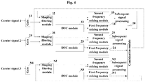
- Fig. 4 is a structural schematic diagram of a digital up conversion processing device provided in some embodiments. As shown in Fig. 4 , the digital up conversion processing device includes: N main body modules and a combination module 20, wherein N is a positive integer greater than or equal to 1.
- Each of the N main body modules includes: a gain module, a shaping filtering module, a DUC module, a first frequency mixing module, and a second frequency mixing module.
- a first main body module includes: a gain module 11, a shaping filtering module 12, a DUC module 13, a first frequency mixing module 14 and a second frequency mixing module 15;
- a second main body module includes: a gain module 21, a shaping filtering module 22, a DUC module 23, a first frequency mixing module 24 and a second frequency mixing module 25; and by analogy, an Nth main body module includes: a gain module N1, a shaping filtering module N2, a DUC module N3, a first frequency mixing module N4 and a second frequency mixing module N5.
- an input end of the gain module 11 inputs a carrier signal, and an output end of the gain module 11 is connected to an input end of the shaping filtering module 12 and an input end of the DUC module 13; an output end of the shaping filtering module 12 is connected to the input end of the DUC module 13 and an input end of the second frequency mixing module 15; an output end of the DUC module 13 is connected to an input end of the first frequency mixing module 14 and the input end of the second frequency mixing module 15; an output end of the second frequency mixing module 15 outputs the carrier signal; an output end of the first frequency mixing module 14 is connected to an input end of the combination module 20; and an output end of the combination module 20 is connected to the input end of the shaping filtering module 12.
- connection relationships of the second main body module, ..., the Nth main body module are similar to the connection relationship of the first main body module, and will not be repeated herein.
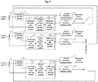
- Fig. 5 is a structural schematic diagram of another digital up conversion processing device provided in some embodiments.
- the DUC module includes M interpolation filtering modules connected in series, wherein M is a positive integer greater than or equal to 1.
- the DUC module 13 includes an interpolation filtering module 131, an interpolation filtering module 132, ..., and an interpolation filtering module 13M;
- the DUC module 23 includes an interpolation filtering module 231, an interpolation filtering module 232, ..., and an interpolation filtering module 23M;
- the DUC module N3 includes an interpolation filtering module N31, an interpolation filtering module N32, ..., and an interpolation filtering module N3M.
- the interpolation filtering modules are double interpolation filters. Assuming that an input data rate of the interpolation filtering module 131 is a, output data rates of the interpolation filtering module 131, the interpolation filtering module 132, ..., and the interpolation filtering module 13M are 2a, 4a, ..., 2ma, respectively.
- the filter order and corresponding filter coefficient of each of the shaping filtering modules are built in and can be selected, thereby satisfying performance requirements for processing signals with different bandwidths and different rates.
- the combination module 20 may be a subband combination module.
- the combination module 20 can combine and add K (K ⁇ N) carriers in N carrier signals according to service requirements and then output the combined carrier signal, and the shaping filtering module which can be connected to the output of the combined carrier signal may be randomly selected from shaping filtering modules connected when the K carriers are outputted without being combined.
- Figs. 4 and 5 do not reflect a subband carrier combination function, that is, Figs. 4 and 5 show a structure when carriers are not subjected to subband combination.
- the gain module is configured to adjust the power of the subband carrier signal and send the subband carrier signal to the DUC module;
- the DUC module is configured to perform digital up conversion processing on the subband carrier signal, and send the subband carrier signal to the first frequency mixing module;
- the first frequency mixing module is configured to perform frequency mixing processing on the subband carrier signal, and send the subband carrier signal to the combination module.
- the combination module is configured to receive the subband carrier signal and send the subband carrier signal to the shaping filtering module of the main body module corresponding to the subband carrier signal;
- the shaping filtering module is configured to perform shaping filtering processing on the subband carrier signal, and send the subband carrier signal to the second frequency mixing module;
- the second frequency mixing module is configured to perform frequency mixing processing on the subband carrier signal.
- a carrier signal 1, a carrier signal 2, ..., and a carrier signal N are subband carrier signals, and the carrier signal 1, the carrier signal 2, ..., and the carrier signal N are not subjected to subband combination, taking the first main body module as an example, a flow direction of the carrier signal 1 is shown by dotted lines in the figure, and in this case, the main body module implements the following functions respectively.
- the gain module 11 is configured to adjust the power of the subband carrier signal, and sends the subband carrier signal to the DUC module 13.
- the DUC module 13 is configured to perform digital up conversion processing on the subband carrier signal, and send the subband carrier signal to the first frequency mixing module 14.
- the first frequency mixing module 14 is configured to perform frequency mixing processing on the subband carrier signal, and send the subband carrier signal to the combination module 20.
- the combination module 20 is configured to receive the subband carrier signal, and send the subband carrier signal to the shaping filtering module of the main body module corresponding to the subband carrier signal (that is, send the subband carrier signal 1 to the shaping filtering module 12, send the subband carrier signal 2 to the shaping filtering module 22, ..., and send the subband carrier signal N to the shaping filtering module N2).
- the shaping filtering module 12 is configured to perform shaping filtering processing on the subband carrier signal, and send the subband carrier signal to the second frequency mixing module 15.
- the second frequency mixing module 15 is configured to perform frequency mixing processing on the subband carrier signal.
- the gain module is configured to adjust the power of the subband carrier signal and send the subband carrier signal to the DUC module.
- the DUC module is configured to perform digital up conversion processing on the subband carrier signal, and send the subband carrier signal to the first frequency mixing module.
- the first frequency mixing module is configured to perform frequency mixing processing on the subband carrier signal, and send the subband carrier signal to the combination module.
- the combination module is configured to receive N subband carrier signals, add and combine K subband carrier signals to obtain a combined subband carrier signal, and send the combined subband carrier signal to a shaping filtering module of the main body module corresponding to any one subband carrier signal among the K subband carrier signals, wherein K is a positive integer less than or equal to N.
- the shaping filtering module is configured to perform shaping filtering processing on the combined subband carrier signal, and send the combined subband carrier signal to the second frequency mixing module.
- the second frequency mixing module is configured to perform frequency mixing processing on the combined subband carrier signal.
- the combination module is further configured to send each uncombined subband carrier signal to the shaping filtering module of the main body module corresponding to the uncombined subband carrier signal.
- the shaping filtering module is further configured to perform shaping filtering processing on the uncombined subband carrier signal, and send the uncombined subband carrier signal to the second frequency mixing module.
- the second frequency mixing module is further configured to perform frequency mixing processing on the uncombined subband carrier signal.
- the carrier signal 1, the carrier signal 2, ..., and the carrier signal N are subband carrier signals, and the carrier signal 1 and the carrier signal 2 are subjected to subband combination, and the carrier signal 3, ..., and the carrier signal N are not subjected to subband combination.
- the main body modules respectively implement the following functions.
- the gain module 11 is configured to adjust the power of the subband carrier signal, and send the subband carrier signal to the DUC module 13.
- the DUC module 13 is configured to perform digital up conversion processing on the subband carrier signal, and send the subband carrier signal to the first frequency mixing module 14.
- the first frequency mixing module 14 is configured to perform frequency mixing processing on the subband carrier signal, and send the subband carrier signal to the combination module 20.
- the gain module 21 is configured to adjust the power of the subband carrier signal, and send the subband carrier signal to the DUC module 23.
- the DUC module 23 is configured to perform digital up conversion processing on the subband carrier signal, and send the subband carrier signal to the first frequency mixing module 24.
- the first frequency mixing module 24 is configured to perform frequency mixing processing on the subband carrier signal, and send the subband carrier signal to the combination module 20.
- the gain module N1 is configured to adjust the power of the subband carrier signal, and send the subband carrier signal to the DUC module N3.
- the DUC module N3 is configured to perform digital up conversion processing on the subband carrier signal, and send the subband carrier signal to the first frequency mixing module N4.
- the first frequency mixing module N4 is configured to perform frequency mixing processing on the subband carrier signal, and send the subband carrier signal to the combination module 20.
- the combination module 20 is configured to receive N subband carrier signals, add and combine the carrier signal 1 and the carrier signal 2 to obtain a combined subband carrier signal, and send the combined subband carrier signal to the shaping filtering module 12 or the shaping filtering module 22 (in some embodiments of the present disclosure, the combined subband carrier signal is sent to the shaping filtering module 12 for illustration).
- the combination module 20 is further configured to send each uncombined subband carrier signal to the shaping filtering module of the main body module corresponding to the uncombined subband carrier signal (that is, send the subband carrier signal 3 to the shaping filtering module 32, ..., and send the subband carrier signal N to the shaping filtering module N2).
- the shaping filtering module 12 is configured to perform shaping filtering processing on the combined subband carrier signal, and send the combined subband carrier signal to the second frequency mixing module 15.
- the second frequency mixing module 15 is configured to perform frequency mixing processing on the combined subband carrier signal.
- the shaping filtering module N2 is configured to perform shaping filtering processing on the uncombined subband carrier signal, and send the uncombined subband carrier signal to the second frequency mixing module N5.
- the second frequency mixing module N5 is configured to perform frequency mixing processing on the uncombined subband carrier signal.
- the gain module is configured to adjust the power of the non-subband carrier signal and send the non-subband carrier signal to the shaping filtering module.
- the shaping filtering module is configured to perform shaping filtering processing on the non-subband carrier signal, and send the non-subband carrier signal to the DUC module.
- the DUC module is configured to perform digital up conversion processing on the non-subband carrier signal, and send the non-subband carrier signal to the second frequency mixing module.
- the second frequency mixing module is configured to perform frequency mixing processing on the non-subband carrier signal.
- the carrier signal 1, the carrier signal 2, ..., and the carrier signal N are non-subband carrier signals, taking the first main body module as an example, a flow direction of the carrier signal 1 is shown by solid lines in the figure, and in this case, the main body module implements the following functions respectively.
- the gain module 11 is configured to adjust the power of the non-subband carrier signal, and send the non-subband carrier signal to the shaping filtering module 12.
- the shaping filtering module 12 is configured to perform shaping filtering processing on the non-subband carrier signal, and send the non-subband carrier signal to the DUC module 13.
- the DUC module 13 is configured to perform digital up conversion processing on the non-subband carrier signal, and send the non-subband carrier signal to the second frequency mixing module 15.
- the second frequency mixing module 15 is configured to perform frequency mixing processing on the non-subband carrier signal.
- the embodiments of the present disclosure provide a digital up conversion processing device, including N main body modules and a combination module, wherein N is a positive integer greater than or equal to 1.
- Each of the N main body modules includes: a gain module, a shaping filtering module, a DUC module, a first frequency mixing module, and a second frequency mixing module.
- An input end of the gain module inputs a carrier signal, and an output end of the gain module is connected to an input end of the shaping filtering module and an input end of the DUC module.
- An output end of the shaping filtering module is connected to the input end of the DUC module and an input end of the second frequency mixing module.
- An output end of the DUC module is connected to an input end of the first frequency mixing module and the input end of the second frequency mixing module.
- An output end of the second frequency mixing module outputs a carrier signal.
- An output end of the first frequency mixing module is connected to an input end of the combination module; and an output end of the combination module is connected to the input end of the shaping filtering module.
- the DUC module is multiplexed while processing both multi-bandwidth subband carrier signals and non-subband carrier signals, which reduces hardware overhead and production costs of the digital up conversion processing device, and achieves low power consumption and miniaturization of the digital up conversion processing device.
- the embodiments of the present disclosure also provide an intermediate frequency link in a wireless communication system.
- the intermediate frequency link includes the digital up conversion processing device provided in any embodiment of the present disclosure.
- the implementation principle and effect of the intermediate frequency link in a wireless communication system provided in this embodiment are similar to those of the described digital up conversion processing device, and will not be repeated herein.
- the digital up conversion processing device is located on a transceiver board unit of the intermediate frequency link in a wireless communication system.
- the described content merely relates to exemplary embodiments of the present disclosure, and is not intended to limit the scope of protection of some embodiments of the present disclosure.
- the multiple embodiments of the present disclosure may be implemented in hardware or dedicated circuit, software, logic, or any combination thereof.
- some aspects may be implemented in hardware, while other aspects may be implemented in firmware or software that may be executed by a controller, a microprocessor or other computing devices, although the present disclosure is not limited thereto.
Landscapes
- Engineering & Computer Science (AREA)
- Computer Networks & Wireless Communication (AREA)
- Signal Processing (AREA)
- Power Engineering (AREA)
- Transceivers (AREA)
Abstract
Description
- The present disclosure claims the priority of
Chinese Patent Application No. 201910935350.X, filed to the China National Intellectual Property Administration on September 29, 2019 - The present disclosure relates to the field of wireless communication networks, and for example, relates to a digital up conversion processing device, and an intermediate frequency link in a wireless communication system.
- A digital up conversion processing device can perform multiple types of power adjustments and rate conversions on an inputted digital signal, achieve modulation and frequency mixing in a digital domain, and output a high-speed digital intermediate frequency signal. In a wireless communication system, some large-bandwidth digital signals sent at a base band can be divided into multiple subband carrier signals, which are then transmitted to an intermediate frequency portion for processing. The digital up conversion processing device generally includes a structure (hereinafter structure I for short) configured to process subband carrier signals and a structure (hereinafter structure II for short) configured to process non-subband carrier signals. The structure I and the structure II are separately provided, causing a high cost and a large volume of the digital up conversion processing device.
- The embodiments of the present disclosure provide a digital up conversion processing device, and an intermediate frequency link in a wireless communication system, which can reduce hardware overhead and production costs of the digital up conversion processing device, and achieve low power consumption and miniaturization of the digital up conversion processing device.
- Provided is a digital up conversion processing device, including N main body modules and a combination module, wherein N is a positive integer greater than or equal to 1; each of the N main body modules includes: a gain module, a shaping filtering module, a Digital Up Converter (DUC) module, a first frequency mixing module, and a second frequency mixing module; wherein
- an input end of the gain module is configured to input a carrier signal, and an output end of the gain module is connected to an input end of the shaping filtering module and an input end of the DUC module;
- an output end of the shaping filtering module is connected to the input end of the DUC module and an input end of the second frequency mixing module;
- an output end of the DUC module is connected to an input end of the first frequency mixing module and the input end of the second frequency mixing module;
- an output end of the second frequency mixing module is configured to output the carrier signal;
- an output end of the first frequency mixing module is connected to an input end of the combination module; and
- an output end of the combination module is connected to the input end of the shaping filtering module.
- Also provided is an intermediate frequency link in a wireless communication system, wherein the intermediate frequency link includes the described digital up conversion processing device.
-
-
Fig. 1 is a structural schematic diagram of a digital up conversion processing device; -
Fig. 2 is a structural schematic diagram of another digital up conversion processing device; -
Fig. 3 is a structural schematic diagram of yet another digital up conversion processing device; -
Fig. 4 is a structural schematic diagram of a digital up conversion processing device provided in some embodiments; and -
Fig. 5 is a structural schematic diagram of another digital up conversion processing device provided in some embodiments. - Hereinafter, the embodiments of the present disclosure will be described in combination with the accompanying drawings.
- A digital up conversion processing device is an important component of a transceiver board unit in a radio remote unit (RRU), and main functions of the digital up conversion processing device are to perform multiple types of power adjustments and rate conversions on an inputted digital signal, achieve modulation and frequency mixing in a digital domain, and output a high-speed digital intermediate frequency signal.
- Generally, large-bandwidth digital signals sent by a building base band unit (BBU) to an RRU may be divided into multiple subband carrier signals, and signal processing flows for the subband carrier signals and non-subband carrier signals in the digital up conversion processing device are different according to their respective characteristics.
-
Fig. 1 is a structural schematic diagram of a digital up conversion processing device. The digital up conversion processing device as shown inFig. 1 is configured to process subband carrier signals. As shown inFig. 1 , the digital up conversion processing device includes: N paths of gains, N paths of multi-stage interpolation filtering modules (also referred to as multi-stage DUC filtering modules, and inFig. 1 , the modules are drawn as M stages as an example), N paths of frequency mixing numerically controlled oscillators (NCOs) 0, a combination module and N paths of shaping filtering modules. When a digital signal is a subband carrier signal, the subband carrier signal first passes through the gain for power adjustment, then passes through the multi-stage interpolation filtering modules to complete digital up conversion processing, and finally passes through the frequency mixing NCO0 and the combination module and enters the shaping filtering module to complete shaping filtering and then is outputted. -
Fig. 2 is a structural schematic diagram of another digital up conversion processing device. The digital up conversion processing device shown inFig. 2 is configured to process non-subband carrier signals. As shown inFig. 2 , the digital up conversion processing device includes: N paths of gains, N paths of shaping filtering modules, N paths of multi-stage interpolation filtering modules (inFig. 2 , the modules are drawn as M stages as an example) and N paths of frequency mixing NCO1. When the digital signal is a non-subband carrier signal, the non-subband carrier signal first passes through the gain for power adjustment, then passes through the shaping filtering module to complete shaping filtering, and finally sequentially passes through the multi-stage interpolation filtering modules and the frequency mixing NCO1 to complete digital up conversion processing and frequency mixing operations. - The described two digital up conversion processing devices separately process subband carrier signals and non-subband carrier signals. The processes for data stream processing and timing control are simple, the multiple processes of carrier processing do not affect each other, and the implementation technology is simple. However, when a system needs to be compatible for multi-bandwidth subband carrier signals and non-subband carrier signals, the digital up conversion processing devices as shown in
Figs. 1 and2 cannot satisfy the requirements.Fig. 3 is a structural schematic diagram of yet another digital up conversion processing device. The digital up conversion processing device includes: N paths of gains, N paths of multi-stage interpolation filtering modules 1 (inFig. 3 , the modules are drawn as M stages as an example), N paths of frequency mixing NCO0, a combination module, N paths of shaping filtering modules, N paths of multi-stage interpolation filtering modules 2 (inFig. 3 , the modules are drawn as M stages as an example), and N paths of frequency mixing NCO1. The digital up conversion processing device shown inFig. 3 also has the advantages of the digital up conversion processing devices as shown inFigs. 1 and2 when processing subband carrier signals and non-subband carrier signals, that is, the timing control is simple and is easy to implement. However, as shown inFig. 3 , the multi-stage interpolation filtering modules achieving the same function appear twice in the implementation structure, and the disadvantages caused thereby include two aspects: on the one hand, the digital up conversion processing device as shown inFig. 3 requires more hardware resources and more interpolation filtering modules, but nowadays, as the product requirements develop towards the directions of low power consumption, miniaturization and microminiaturization, the digital up conversion processing device as shown inFig. 3 cannot meet the requirements; and on the other hand, the digital up conversion processing device as shown inFig. 3 prolongs the product development time, and a lot of hardware overheads also significantly increase the system power consumption. In a multi-bandwidth multi-carrier communication system, the described disadvantages become more and more fatal and obvious, which weakens the product competitiveness to a great extent. - Embodiments of the present disclosure provide a digital up conversion processing device, and an intermediate frequency link in a wireless communication system, which can reduce hardware overhead and production costs of the digital up conversion processing device, and achieve low power consumption and miniaturization of the digital up conversion processing device.
- The terms "first", "second", "third", and the like herein are used to distinguish different objects, and are not to define a specific sequence. The following multiple embodiments of the present disclosure may be executed separately, or the multiple embodiments may be executed in combination with each other, which is not limited in the embodiments of the present disclosure.
- Hereinafter, a digital up conversion processing device, an intermediate frequency link in a wireless communication system, and effects thereof are described.
-
Fig. 4 is a structural schematic diagram of a digital up conversion processing device provided in some embodiments. As shown inFig. 4 , the digital up conversion processing device includes: N main body modules and acombination module 20, wherein N is a positive integer greater than or equal to 1. - Each of the N main body modules includes: a gain module, a shaping filtering module, a DUC module, a first frequency mixing module, and a second frequency mixing module. As shown in
Fig. 4 , a first main body module includes: a gain module 11, ashaping filtering module 12, aDUC module 13, a firstfrequency mixing module 14 and a secondfrequency mixing module 15; a second main body module includes: again module 21, ashaping filtering module 22, aDUC module 23, a firstfrequency mixing module 24 and a secondfrequency mixing module 25; and by analogy, an Nth main body module includes: a gain module N1, a shaping filtering module N2, a DUC module N3, a first frequency mixing module N4 and a second frequency mixing module N5. - Taking the first main body module as an example, an input end of the gain module 11 inputs a carrier signal, and an output end of the gain module 11 is connected to an input end of the
shaping filtering module 12 and an input end of theDUC module 13; an output end of theshaping filtering module 12 is connected to the input end of theDUC module 13 and an input end of the secondfrequency mixing module 15; an output end of theDUC module 13 is connected to an input end of the firstfrequency mixing module 14 and the input end of the secondfrequency mixing module 15; an output end of the secondfrequency mixing module 15 outputs the carrier signal; an output end of the firstfrequency mixing module 14 is connected to an input end of thecombination module 20; and an output end of thecombination module 20 is connected to the input end of theshaping filtering module 12. - The connection relationships of the second main body module, ..., the Nth main body module are similar to the connection relationship of the first main body module, and will not be repeated herein.
- In some embodiments, in combination with
Fig. 4 ,Fig. 5 is a structural schematic diagram of another digital up conversion processing device provided in some embodiments. As shown inFig. 5 , the DUC module includes M interpolation filtering modules connected in series, wherein M is a positive integer greater than or equal to 1. That is, theDUC module 13 includes aninterpolation filtering module 131, aninterpolation filtering module 132, ..., and aninterpolation filtering module 13M; theDUC module 23 includes aninterpolation filtering module 231, aninterpolation filtering module 232, ..., and aninterpolation filtering module 23M; and by analogy, the DUC module N3 includes an interpolation filtering module N31, an interpolation filtering module N32, ..., and an interpolation filtering module N3M. - In some embodiments, the interpolation filtering modules are double interpolation filters. Assuming that an input data rate of the
interpolation filtering module 131 is a, output data rates of theinterpolation filtering module 131, theinterpolation filtering module 132, ..., and theinterpolation filtering module 13M are 2a, 4a, ..., 2ma, respectively. - In some embodiments, the filter order and corresponding filter coefficient of each of the shaping filtering modules are built in and can be selected, thereby satisfying performance requirements for processing signals with different bandwidths and different rates.
- In some embodiments, the
combination module 20 may be a subband combination module. Thecombination module 20 can combine and add K (K≤N) carriers in N carrier signals according to service requirements and then output the combined carrier signal, and the shaping filtering module which can be connected to the output of the combined carrier signal may be randomly selected from shaping filtering modules connected when the K carriers are outputted without being combined.Figs. 4 and5 do not reflect a subband carrier combination function, that is,Figs. 4 and5 show a structure when carriers are not subjected to subband combination. - In some embodiments, if the carrier signal is a subband carrier signal, the gain module is configured to adjust the power of the subband carrier signal and send the subband carrier signal to the DUC module; the DUC module is configured to perform digital up conversion processing on the subband carrier signal, and send the subband carrier signal to the first frequency mixing module; the first frequency mixing module is configured to perform frequency mixing processing on the subband carrier signal, and send the subband carrier signal to the combination module.
- The combination module is configured to receive the subband carrier signal and send the subband carrier signal to the shaping filtering module of the main body module corresponding to the subband carrier signal; the shaping filtering module is configured to perform shaping filtering processing on the subband carrier signal, and send the subband carrier signal to the second frequency mixing module; and the second frequency mixing module is configured to perform frequency mixing processing on the subband carrier signal.
- Refer to
Fig. 5 , if acarrier signal 1, acarrier signal 2, ..., and a carrier signal N are subband carrier signals, and thecarrier signal 1, thecarrier signal 2, ..., and the carrier signal N are not subjected to subband combination, taking the first main body module as an example, a flow direction of thecarrier signal 1 is shown by dotted lines in the figure, and in this case, the main body module implements the following functions respectively. - The gain module 11 is configured to adjust the power of the subband carrier signal, and sends the subband carrier signal to the
DUC module 13. TheDUC module 13 is configured to perform digital up conversion processing on the subband carrier signal, and send the subband carrier signal to the firstfrequency mixing module 14. The firstfrequency mixing module 14 is configured to perform frequency mixing processing on the subband carrier signal, and send the subband carrier signal to thecombination module 20. thecombination module 20 is configured to receive the subband carrier signal, and send the subband carrier signal to the shaping filtering module of the main body module corresponding to the subband carrier signal (that is, send thesubband carrier signal 1 to the shapingfiltering module 12, send thesubband carrier signal 2 to the shapingfiltering module 22, ..., and send the subband carrier signal N to the shaping filtering module N2). The shapingfiltering module 12 is configured to perform shaping filtering processing on the subband carrier signal, and send the subband carrier signal to the secondfrequency mixing module 15. The secondfrequency mixing module 15 is configured to perform frequency mixing processing on the subband carrier signal. - In some embodiments, if the carrier signal is a subband carrier signal, the gain module is configured to adjust the power of the subband carrier signal and send the subband carrier signal to the DUC module. The DUC module is configured to perform digital up conversion processing on the subband carrier signal, and send the subband carrier signal to the first frequency mixing module. The first frequency mixing module is configured to perform frequency mixing processing on the subband carrier signal, and send the subband carrier signal to the combination module.
- The combination module is configured to receive N subband carrier signals, add and combine K subband carrier signals to obtain a combined subband carrier signal, and send the combined subband carrier signal to a shaping filtering module of the main body module corresponding to any one subband carrier signal among the K subband carrier signals, wherein K is a positive integer less than or equal to N. The shaping filtering module is configured to perform shaping filtering processing on the combined subband carrier signal, and send the combined subband carrier signal to the second frequency mixing module. The second frequency mixing module is configured to perform frequency mixing processing on the combined subband carrier signal.
- The combination module is further configured to send each uncombined subband carrier signal to the shaping filtering module of the main body module corresponding to the uncombined subband carrier signal. The shaping filtering module is further configured to perform shaping filtering processing on the uncombined subband carrier signal, and send the uncombined subband carrier signal to the second frequency mixing module. The second frequency mixing module is further configured to perform frequency mixing processing on the uncombined subband carrier signal.
- Refer to
Fig. 5 , if thecarrier signal 1, thecarrier signal 2, ..., and the carrier signal N are subband carrier signals, and thecarrier signal 1 and thecarrier signal 2 are subjected to subband combination, and thecarrier signal 3, ..., and the carrier signal N are not subjected to subband combination. By taking the first main body module, the second main body module, and the Nth main body module as an example, flow directions of thecarrier signal 1, thecarrier signal 2, and the carrier signal N are shown by dotted lines in the figure, and at this time, the main body modules respectively implement the following functions. - The gain module 11 is configured to adjust the power of the subband carrier signal, and send the subband carrier signal to the
DUC module 13. TheDUC module 13 is configured to perform digital up conversion processing on the subband carrier signal, and send the subband carrier signal to the firstfrequency mixing module 14. The firstfrequency mixing module 14 is configured to perform frequency mixing processing on the subband carrier signal, and send the subband carrier signal to thecombination module 20. - The
gain module 21 is configured to adjust the power of the subband carrier signal, and send the subband carrier signal to theDUC module 23. TheDUC module 23 is configured to perform digital up conversion processing on the subband carrier signal, and send the subband carrier signal to the firstfrequency mixing module 24. The firstfrequency mixing module 24 is configured to perform frequency mixing processing on the subband carrier signal, and send the subband carrier signal to thecombination module 20. - The gain module N1 is configured to adjust the power of the subband carrier signal, and send the subband carrier signal to the DUC module N3. The DUC module N3 is configured to perform digital up conversion processing on the subband carrier signal, and send the subband carrier signal to the first frequency mixing module N4. The first frequency mixing module N4 is configured to perform frequency mixing processing on the subband carrier signal, and send the subband carrier signal to the
combination module 20. - The
combination module 20 is configured to receive N subband carrier signals, add and combine thecarrier signal 1 and thecarrier signal 2 to obtain a combined subband carrier signal, and send the combined subband carrier signal to the shapingfiltering module 12 or the shaping filtering module 22 (in some embodiments of the present disclosure, the combined subband carrier signal is sent to the shapingfiltering module 12 for illustration). In addition, thecombination module 20 is further configured to send each uncombined subband carrier signal to the shaping filtering module of the main body module corresponding to the uncombined subband carrier signal (that is, send thesubband carrier signal 3 to the shaping filtering module 32, ..., and send the subband carrier signal N to the shaping filtering module N2). - The shaping
filtering module 12 is configured to perform shaping filtering processing on the combined subband carrier signal, and send the combined subband carrier signal to the secondfrequency mixing module 15. The secondfrequency mixing module 15 is configured to perform frequency mixing processing on the combined subband carrier signal. - The shaping filtering module N2 is configured to perform shaping filtering processing on the uncombined subband carrier signal, and send the uncombined subband carrier signal to the second frequency mixing module N5. The second frequency mixing module N5 is configured to perform frequency mixing processing on the uncombined subband carrier signal.
- In some embodiments, if the carrier signal is a non-subband carrier signal, the gain module is configured to adjust the power of the non-subband carrier signal and send the non-subband carrier signal to the shaping filtering module. the shaping filtering module is configured to perform shaping filtering processing on the non-subband carrier signal, and send the non-subband carrier signal to the DUC module. The DUC module is configured to perform digital up conversion processing on the non-subband carrier signal, and send the non-subband carrier signal to the second frequency mixing module. The second frequency mixing module is configured to perform frequency mixing processing on the non-subband carrier signal.
- Refer to
Fig. 5 , if thecarrier signal 1, thecarrier signal 2, ..., and the carrier signal N are non-subband carrier signals, taking the first main body module as an example, a flow direction of thecarrier signal 1 is shown by solid lines in the figure, and in this case, the main body module implements the following functions respectively. - The gain module 11 is configured to adjust the power of the non-subband carrier signal, and send the non-subband carrier signal to the shaping
filtering module 12. The shapingfiltering module 12 is configured to perform shaping filtering processing on the non-subband carrier signal, and send the non-subband carrier signal to theDUC module 13. TheDUC module 13 is configured to perform digital up conversion processing on the non-subband carrier signal, and send the non-subband carrier signal to the secondfrequency mixing module 15. The secondfrequency mixing module 15 is configured to perform frequency mixing processing on the non-subband carrier signal. - The embodiments of the present disclosure provide a digital up conversion processing device, including N main body modules and a combination module, wherein N is a positive integer greater than or equal to 1. Each of the N main body modules includes: a gain module, a shaping filtering module, a DUC module, a first frequency mixing module, and a second frequency mixing module. An input end of the gain module inputs a carrier signal, and an output end of the gain module is connected to an input end of the shaping filtering module and an input end of the DUC module. An output end of the shaping filtering module is connected to the input end of the DUC module and an input end of the second frequency mixing module. An output end of the DUC module is connected to an input end of the first frequency mixing module and the input end of the second frequency mixing module. An output end of the second frequency mixing module outputs a carrier signal. An output end of the first frequency mixing module is connected to an input end of the combination module; and an output end of the combination module is connected to the input end of the shaping filtering module. Compared with the digital up conversion processing device in the related art, the DUC module is multiplexed while processing both multi-bandwidth subband carrier signals and non-subband carrier signals, which reduces hardware overhead and production costs of the digital up conversion processing device, and achieves low power consumption and miniaturization of the digital up conversion processing device.
- The embodiments of the present disclosure also provide an intermediate frequency link in a wireless communication system. The intermediate frequency link includes the digital up conversion processing device provided in any embodiment of the present disclosure. The implementation principle and effect of the intermediate frequency link in a wireless communication system provided in this embodiment are similar to those of the described digital up conversion processing device, and will not be repeated herein.
- In some embodiments, the digital up conversion processing device is located on a transceiver board unit of the intermediate frequency link in a wireless communication system.
- The described content merely relates to exemplary embodiments of the present disclosure, and is not intended to limit the scope of protection of some embodiments of the present disclosure. In general, the multiple embodiments of the present disclosure may be implemented in hardware or dedicated circuit, software, logic, or any combination thereof. For example, some aspects may be implemented in hardware, while other aspects may be implemented in firmware or software that may be executed by a controller, a microprocessor or other computing devices, although the present disclosure is not limited thereto.
Claims (10)
- A digital up conversion processing device, comprising: N main body modules and a combination module, wherein N is a positive integer greater than or equal to 1; each of the N main body modules comprises: a gain module, a shaping filtering module, a Digital Up Converter, DUC, module, a first frequency mixing module, and a second frequency mixing module; whereinan input end of the gain module is configured to input a carrier signal, and an output end of the gain module is connected to an input end of the shaping filtering module and an input end of the DUC module;an output end of the shaping filtering module is connected to the input end of the DUC module and an input end of the second frequency mixing module;an output end of the DUC module is connected to an input end of the first frequency mixing module and the input end of the second frequency mixing module;an output end of the second frequency mixing module is configured to output the carrier signal;an output end of the first frequency mixing module is connected to an input end of the combination module; andan output end of the combination module is connected to the input end of the shaping filtering module.
- The digital up conversion processing device according to claim 1, wherein the DUC module comprises M interpolation filtering modules connected in series, wherein M is a positive integer greater than or equal to 1.
- The digital up conversion processing device according to claim 2, wherein each of the M interpolation filtering modules is a double interpolation filter.
- The digital up conversion processing device according to claim 1, wherein in cases where the carrier signal is a subband carrier signal,the gain module is configured to adjust the power of the subband carrier signal and send the subband carrier signal to the DUC module;the DUC module is configured to perform digital up conversion processing on the subband carrier signal, and send the subband carrier signal to the first frequency mixing module; andthe first frequency mixing module is configured to perform frequency mixing processing on the subband carrier signal, and send the subband carrier signal to the combination module.
- The digital up conversion processing device according to claim 4, whereinthe combination module is configured to receive the subband carrier signal and send the subband carrier signal to the shaping filtering module of the main body module corresponding to the subband carrier signal;the shaping filtering module is configured to perform shaping filtering processing on the subband carrier signal, and send the subband carrier signal to the second frequency mixing module; andthe second frequency mixing module is configured to perform frequency mixing processing on the subband carrier signal.
- The digital up conversion processing device according to claim 4, whereinthe combination module is configured to receive N subband carrier signals, add and combine K subband carrier signals in the N subband carrier signals to obtain a combined subband carrier signal, and send the combined subband carrier signal to the shaping filtering module of the main body module corresponding to one subband carrier signal among the K subband carrier signals, wherein K is a positive integer less than or equal to N;the shaping filtering module is configured to perform shaping filtering processing on the combined subband carrier signal, and send the combined subband carrier signal to the second frequency mixing module; andthe second frequency mixing module is configured to perform frequency mixing processing on the combined subband carrier signal.
- The digital up conversion processing device according to claim 6, whereinthe combination module is further configured to send each uncombined subband carrier signal to the shaping filtering module of the main body module corresponding to the uncombined subband carrier signal;the shaping filtering module is further configured to perform shaping filtering processing on the uncombined subband carrier signal, and send the uncombined subband carrier signal to the second frequency mixing module; andthe second frequency mixing module is configured to perform frequency mixing processing on the uncombined subband carrier signal.
- The digital up conversion processing device according to claim 1, wherein in cases where the carrier signal is a non-subband carrier signal,the gain module is configured to adjust the power of the non-subband carrier signal and send the non-subband carrier signal to the shaping filtering module;the shaping filtering module is configured to perform shaping filtering processing on the non-subband carrier signal, and send the non-subband carrier signal to the DUC module;the DUC module is configured to perform digital up conversion processing on the non-subband carrier signal, and send the non-subband carrier signal to the second frequency mixing module; andthe second frequency mixing module is configured to perform frequency mixing processing on the non-subband carrier signal.
- An intermediate frequency link in a wireless communication system, wherein the intermediate frequency link comprises the digital up conversion processing device according to any one of claims 1-8.
- The intermediate frequency link in the wireless communication system according to claim 9, wherein the digital up conversion processing device is located on a transceiver board unit of the intermediate frequency link in a wireless communication system.
Applications Claiming Priority (2)
| Application Number | Priority Date | Filing Date | Title |
|---|---|---|---|
| CN201910935350.XA CN112583423B (en) | 2019-09-29 | 2019-09-29 | Digital up-conversion processing device and intermediate frequency link of wireless communication system |
| PCT/CN2020/116174 WO2021057617A1 (en) | 2019-09-29 | 2020-09-18 | Digital up converser processing device and intermediate frequency link in wireless communication system |
Publications (3)
| Publication Number | Publication Date |
|---|---|
| EP3937385A1 true EP3937385A1 (en) | 2022-01-12 |
| EP3937385A4 EP3937385A4 (en) | 2022-07-06 |
| EP3937385B1 EP3937385B1 (en) | 2026-04-08 |
Family
ID=75111260
Family Applications (1)
| Application Number | Title | Priority Date | Filing Date |
|---|---|---|---|
| EP20869154.3A Active EP3937385B1 (en) | 2019-09-29 | 2020-09-18 | Digital up converser processing device and intermediate frequency link in wireless communication system |
Country Status (3)
| Country | Link |
|---|---|
| EP (1) | EP3937385B1 (en) |
| CN (1) | CN112583423B (en) |
| WO (1) | WO2021057617A1 (en) |
Cited By (1)
| Publication number | Priority date | Publication date | Assignee | Title |
|---|---|---|---|---|
| GB2642781A (en) * | 2022-05-24 | 2026-01-21 | Evertz Microsystems Ltd | Multi-stage digital converters |
Family Cites Families (16)
| Publication number | Priority date | Publication date | Assignee | Title |
|---|---|---|---|---|
| CN1124756C (en) * | 2000-11-14 | 2003-10-15 | 华为技术有限公司 | Gain equalizing method and device based on wide band multiple carrier base station |
| KR100446540B1 (en) * | 2001-04-16 | 2004-09-01 | 삼성전자주식회사 | Transmitter for a data communication |
| US6987953B2 (en) * | 2003-03-31 | 2006-01-17 | Nortel Networks Limited | Digital transmitter and method |
| KR100628741B1 (en) * | 2004-11-25 | 2006-09-29 | 엘지노텔 주식회사 | Digital Combined Multicarrier Transmitter in Mobile Communication System and Its Method |
| CN100550627C (en) * | 2005-07-07 | 2009-10-14 | 中兴通讯股份有限公司 | A multi-carrier signal peak clipping device and method using preprocessing technology |
| KR100780669B1 (en) * | 2006-03-30 | 2007-11-30 | 포스데이타 주식회사 | Digital frequency upconversion device and method |
| CN101197606B (en) * | 2006-12-04 | 2012-03-07 | 京信通信技术(广州)有限公司 | Digital intermediate frequency conversion method and system used in repeater |
| CN101119356B (en) * | 2007-07-10 | 2012-10-17 | 京信通信系统(中国)有限公司 | Multi-channel digital up-conversion system and digital up-conversion method |
| CN100593913C (en) * | 2007-07-31 | 2010-03-10 | 京信通信系统(中国)有限公司 | Multi-carrier transmitter and multi-carrier transmission method based on digital intermediate frequency technology |
| CN101399600A (en) * | 2007-09-29 | 2009-04-01 | 京信通信系统(中国)有限公司 | Multi-carrier digital frequency selecting antenna repeater system and multi-carrier digital frequency selecting method thereof |
| CN101257481B (en) * | 2008-04-22 | 2012-09-05 | 中兴通讯股份有限公司 | System and method for cutting peak of preprocess discontinuousness allocating multiple carrier waves |
| CN101369881B (en) * | 2008-09-27 | 2011-09-14 | 京信通信系统(中国)有限公司 | Multi-carrier digital frequency-selection system and its signal processing method |
| CN201369715Y (en) * | 2009-03-18 | 2009-12-23 | 京信通信系统(中国)有限公司 | Digital frequency selective system with function of fluctuation adjustment |
| CN106972833B (en) * | 2017-02-28 | 2020-08-18 | 深圳市鼎阳科技股份有限公司 | Digital up-converter capable of resampling by any multiple |
| CN107682098B (en) * | 2017-11-06 | 2020-07-28 | 北京理工大学 | Method for calibrating transmission channel of spaceborne multi-beam antenna without service interruption |
| CN110098803B (en) * | 2019-03-28 | 2023-05-30 | 鹤壁天海电子信息系统有限公司 | Digital up-conversion system and multi-carrier intermediate frequency combining circuit |
-
2019
- 2019-09-29 CN CN201910935350.XA patent/CN112583423B/en active Active
-
2020
- 2020-09-18 WO PCT/CN2020/116174 patent/WO2021057617A1/en not_active Ceased
- 2020-09-18 EP EP20869154.3A patent/EP3937385B1/en active Active
Cited By (2)
| Publication number | Priority date | Publication date | Assignee | Title |
|---|---|---|---|---|
| GB2642781A (en) * | 2022-05-24 | 2026-01-21 | Evertz Microsystems Ltd | Multi-stage digital converters |
| US12580604B2 (en) | 2022-05-24 | 2026-03-17 | Evertz Microsystems Ltd. | Multi-stage digital converters |
Also Published As
| Publication number | Publication date |
|---|---|
| WO2021057617A1 (en) | 2021-04-01 |
| CN112583423B (en) | 2023-08-04 |
| EP3937385A4 (en) | 2022-07-06 |
| CN112583423A (en) | 2021-03-30 |
| EP3937385B1 (en) | 2026-04-08 |
Similar Documents
| Publication | Publication Date | Title |
|---|---|---|
| US20240405733A1 (en) | Multi-mode power amplifier system and related wireless devices and methods | |
| US10128918B2 (en) | Universal remote radio head | |
| EP3944510A1 (en) | Radio frequency front end circuit and mobile terminal | |
| CN103916172B (en) | A kind of RF transceiver and radio frequency transmit-receive method | |
| US10560132B2 (en) | Reconfigurable transmitter and receiver, and methods for reconfiguring | |
| KR20080110553A (en) | Single chip wireless transceiver | |
| CN109450496B (en) | Antenna sharing system, terminal | |
| EP3937385B1 (en) | Digital up converser processing device and intermediate frequency link in wireless communication system | |
| WO2023197662A1 (en) | Dual-transmitting radio frequency circuit and electronic device | |
| CN102098255A (en) | Method, device and base station for signal combination clipping | |
| CN102457292B (en) | Terminal equipment | |
| KR101795090B1 (en) | Process and apparatus for reducing emi in the rf subsystem of a wireless communication system | |
| CN204350042U (en) | There is the shift frequency device of bandwidth varying | |
| CN208046596U (en) | A kind of transmission channel signal processing system for multi-channel digital TR components | |
| CN111106841B (en) | 5G signal processing device of multichannel high rate | |
| CN102457858B (en) | Base station equipment | |
| US9793938B2 (en) | Intermediate-frequency analogue-to-digital conversion device | |
| CN105119618B (en) | A kind of GSM R IF process modules of multichannel | |
| CN114124134B (en) | TDD transmitting and receiving method, device, system and storage medium | |
| CN117014028A (en) | A frequency-agile component system for scatter communications | |
| CN114466434B (en) | A method for transmitting information and a communication device | |
| CN113872616B (en) | Communication device and communication method | |
| CN205195697U (en) | GSM -R intermediate frequency processing module of multichannel | |
| US9356599B1 (en) | Differential driver circuit having bias equalizing pre-drivers | |
| CN115176426A (en) | Radio frequency circuit, signal feedback circuit and communication system |
Legal Events
| Date | Code | Title | Description |
|---|---|---|---|
| STAA | Information on the status of an ep patent application or granted ep patent |
Free format text: STATUS: THE INTERNATIONAL PUBLICATION HAS BEEN MADE |
|
| PUAI | Public reference made under article 153(3) epc to a published international application that has entered the european phase |
Free format text: ORIGINAL CODE: 0009012 |
|
| STAA | Information on the status of an ep patent application or granted ep patent |
Free format text: STATUS: REQUEST FOR EXAMINATION WAS MADE |
|
| 17P | Request for examination filed |
Effective date: 20211008 |
|
| AK | Designated contracting states |
Kind code of ref document: A1 Designated state(s): AL AT BE BG CH CY CZ DE DK EE ES FI FR GB GR HR HU IE IS IT LI LT LU LV MC MK MT NL NO PL PT RO RS SE SI SK SM TR |
|
| A4 | Supplementary search report drawn up and despatched |
Effective date: 20220602 |
|
| RIC1 | Information provided on ipc code assigned before grant |
Ipc: H04B 1/00 20060101ALI20220527BHEP Ipc: H04B 7/00 20060101ALI20220527BHEP Ipc: H04B 1/04 20060101AFI20220527BHEP |
|
| DAV | Request for validation of the european patent (deleted) | ||
| DAX | Request for extension of the european patent (deleted) | ||
| GRAP | Despatch of communication of intention to grant a patent |
Free format text: ORIGINAL CODE: EPIDOSNIGR1 |
|
| STAA | Information on the status of an ep patent application or granted ep patent |
Free format text: STATUS: GRANT OF PATENT IS INTENDED |
|
| INTG | Intention to grant announced |
Effective date: 20260105 |
|
| GRAS | Grant fee paid |
Free format text: ORIGINAL CODE: EPIDOSNIGR3 |
|
| GRAA | (expected) grant |
Free format text: ORIGINAL CODE: 0009210 |
|
| STAA | Information on the status of an ep patent application or granted ep patent |
Free format text: STATUS: THE PATENT HAS BEEN GRANTED |
|
| AK | Designated contracting states |
Kind code of ref document: B1 Designated state(s): AL AT BE BG CH CY CZ DE DK EE ES FI FR GB GR HR HU IE IS IT LI LT LU LV MC MK MT NL NO PL PT RO RS SE SI SK SM TR |
|
| REG | Reference to a national code |
Ref country code: CH Ref legal event code: F10 Free format text: ST27 STATUS EVENT CODE: U-0-0-F10-F00 (AS PROVIDED BY THE NATIONAL OFFICE) Effective date: 20260408 Ref country code: GB Ref legal event code: FG4D |
|
| REG | Reference to a national code |
Ref country code: DE Ref legal event code: R096 Ref document number: 602020070181 Country of ref document: DE |