EP3937327A1 - Multi-power supply monitoring, operation, and control - Google Patents
Multi-power supply monitoring, operation, and control Download PDFInfo
- Publication number
- EP3937327A1 EP3937327A1 EP21183897.4A EP21183897A EP3937327A1 EP 3937327 A1 EP3937327 A1 EP 3937327A1 EP 21183897 A EP21183897 A EP 21183897A EP 3937327 A1 EP3937327 A1 EP 3937327A1
- Authority
- EP
- European Patent Office
- Prior art keywords
- input voltage
- circuit path
- switch
- input
- power supply
- Prior art date
- Legal status (The legal status is an assumption and is not a legal conclusion. Google has not performed a legal analysis and makes no representation as to the accuracy of the status listed.)
- Pending
Links
Images






Classifications
-
- H—ELECTRICITY
- H02—GENERATION; CONVERSION OR DISTRIBUTION OF ELECTRIC POWER
- H02J—ELECTRIC POWER NETWORKS; CIRCUIT ARRANGEMENTS OR SYSTEMS FOR SUPPLYING OR DISTRIBUTING ELECTRIC POWER; SYSTEMS FOR STORING ELECTRIC ENERGY
- H02J1/00—Circuit arrangements for DC mains or DC distribution networks
- H02J1/10—Parallel operation of DC sources
- H02J1/102—Parallel operation of DC sources being switching converters
-
- G—PHYSICS
- G01—MEASURING; TESTING
- G01R—MEASURING ELECTRIC VARIABLES; MEASURING MAGNETIC VARIABLES
- G01R31/00—Arrangements for testing electric properties; Arrangements for locating electric faults; Arrangements for electrical testing characterised by what is being tested not provided for elsewhere
- G01R31/40—Testing power supplies
-
- H—ELECTRICITY
- H02—GENERATION; CONVERSION OR DISTRIBUTION OF ELECTRIC POWER
- H02J—ELECTRIC POWER NETWORKS; CIRCUIT ARRANGEMENTS OR SYSTEMS FOR SUPPLYING OR DISTRIBUTING ELECTRIC POWER; SYSTEMS FOR STORING ELECTRIC ENERGY
- H02J1/00—Circuit arrangements for DC mains or DC distribution networks
- H02J1/08—Three-wire DC power distribution systems; Systems having more than three wires
- H02J1/084—Three-wire DC power distribution systems; Systems having more than three wires for selectively connecting the load or loads to one or several among a plurality of power lines or power sources
-
- G—PHYSICS
- G01—MEASURING; TESTING
- G01R—MEASURING ELECTRIC VARIABLES; MEASURING MAGNETIC VARIABLES
- G01R19/00—Arrangements for measuring currents or voltages or for indicating presence or sign thereof
- G01R19/165—Indicating that current or voltage is either above or below a predetermined value or within or outside a predetermined range of values
- G01R19/16528—Indicating that current or voltage is either above or below a predetermined value or within or outside a predetermined range of values using digital techniques or performing arithmetic operations
-
- G—PHYSICS
- G05—CONTROLLING; REGULATING
- G05F—SYSTEMS FOR REGULATING ELECTRIC OR MAGNETIC VARIABLES
- G05F1/00—Automatic systems in which deviations of an electric quantity from one or more predetermined values are detected at the output of the system and fed back to a device within the system to restore the detected quantity to its predetermined value or values, i.e. retroactive systems
- G05F1/10—Regulating voltage or current
- G05F1/46—Regulating voltage or current wherein the variable actually regulated by the final control device is DC
- G05F1/462—Regulating voltage or current wherein the variable actually regulated by the final control device is DC as a function of the requirements of the load, e.g. delay, temperature, specific voltage/current characteristic
- G05F1/465—Internal voltage generators for integrated circuits, e.g. step down generators
-
- G—PHYSICS
- G05—CONTROLLING; REGULATING
- G05F—SYSTEMS FOR REGULATING ELECTRIC OR MAGNETIC VARIABLES
- G05F1/00—Automatic systems in which deviations of an electric quantity from one or more predetermined values are detected at the output of the system and fed back to a device within the system to restore the detected quantity to its predetermined value or values, i.e. retroactive systems
- G05F1/66—Regulating electric power
-
- G—PHYSICS
- G06—COMPUTING OR CALCULATING; COUNTING
- G06F—ELECTRIC DIGITAL DATA PROCESSING
- G06F1/00—Details not covered by groups G06F3/00 - G06F13/00 and G06F21/00
- G06F1/26—Power supply means, e.g. regulation thereof
-
- G—PHYSICS
- G06—COMPUTING OR CALCULATING; COUNTING
- G06F—ELECTRIC DIGITAL DATA PROCESSING
- G06F1/00—Details not covered by groups G06F3/00 - G06F13/00 and G06F21/00
- G06F1/26—Power supply means, e.g. regulation thereof
- G06F1/263—Arrangements for using multiple switchable power supplies, e.g. battery and AC
-
- G—PHYSICS
- G06—COMPUTING OR CALCULATING; COUNTING
- G06F—ELECTRIC DIGITAL DATA PROCESSING
- G06F1/00—Details not covered by groups G06F3/00 - G06F13/00 and G06F21/00
- G06F1/26—Power supply means, e.g. regulation thereof
- G06F1/28—Supervision thereof, e.g. detecting power-supply failure by out of limits supervision
-
- H—ELECTRICITY
- H02—GENERATION; CONVERSION OR DISTRIBUTION OF ELECTRIC POWER
- H02J—ELECTRIC POWER NETWORKS; CIRCUIT ARRANGEMENTS OR SYSTEMS FOR SUPPLYING OR DISTRIBUTING ELECTRIC POWER; SYSTEMS FOR STORING ELECTRIC ENERGY
- H02J1/00—Circuit arrangements for DC mains or DC distribution networks
- H02J1/08—Three-wire DC power distribution systems; Systems having more than three wires
- H02J1/082—DC supplies with two or more different DC voltage levels
-
- H—ELECTRICITY
- H02—GENERATION; CONVERSION OR DISTRIBUTION OF ELECTRIC POWER
- H02J—ELECTRIC POWER NETWORKS; CIRCUIT ARRANGEMENTS OR SYSTEMS FOR SUPPLYING OR DISTRIBUTING ELECTRIC POWER; SYSTEMS FOR STORING ELECTRIC ENERGY
- H02J1/00—Circuit arrangements for DC mains or DC distribution networks
- H02J1/10—Parallel operation of DC sources
- H02J1/108—Parallel operation of DC sources having arrangements for blocking reverse current flow, e.g. using diodes
-
- H—ELECTRICITY
- H02—GENERATION; CONVERSION OR DISTRIBUTION OF ELECTRIC POWER
- H02M—APPARATUS FOR CONVERSION BETWEEN AC AND AC, BETWEEN AC AND DC, OR BETWEEN DC AND DC, AND FOR USE WITH MAINS OR SIMILAR POWER SUPPLY SYSTEMS; CONVERSION OF DC OR AC INPUT POWER INTO SURGE OUTPUT POWER; CONTROL OR REGULATION THEREOF
- H02M1/00—Details of apparatus for conversion
- H02M1/08—Circuits specially adapted for the generation of control voltages for semiconductor devices incorporated in static converters
-
- H—ELECTRICITY
- H02—GENERATION; CONVERSION OR DISTRIBUTION OF ELECTRIC POWER
- H02M—APPARATUS FOR CONVERSION BETWEEN AC AND AC, BETWEEN AC AND DC, OR BETWEEN DC AND DC, AND FOR USE WITH MAINS OR SIMILAR POWER SUPPLY SYSTEMS; CONVERSION OF DC OR AC INPUT POWER INTO SURGE OUTPUT POWER; CONTROL OR REGULATION THEREOF
- H02M1/00—Details of apparatus for conversion
- H02M1/36—Means for starting or stopping converters
-
- H—ELECTRICITY
- H02—GENERATION; CONVERSION OR DISTRIBUTION OF ELECTRIC POWER
- H02M—APPARATUS FOR CONVERSION BETWEEN AC AND AC, BETWEEN AC AND DC, OR BETWEEN DC AND DC, AND FOR USE WITH MAINS OR SIMILAR POWER SUPPLY SYSTEMS; CONVERSION OF DC OR AC INPUT POWER INTO SURGE OUTPUT POWER; CONTROL OR REGULATION THEREOF
- H02M3/00—Conversion of DC power input into DC power output
- H02M3/02—Conversion of DC power input into DC power output without intermediate conversion into AC
- H02M3/04—Conversion of DC power input into DC power output without intermediate conversion into AC by static converters
- H02M3/10—Conversion of DC power input into DC power output without intermediate conversion into AC by static converters using discharge tubes with control electrode or semiconductor devices with control electrode
- H02M3/145—Conversion of DC power input into DC power output without intermediate conversion into AC by static converters using discharge tubes with control electrode or semiconductor devices with control electrode using devices of a triode or transistor type requiring continuous application of a control signal
- H02M3/155—Conversion of DC power input into DC power output without intermediate conversion into AC by static converters using discharge tubes with control electrode or semiconductor devices with control electrode using devices of a triode or transistor type requiring continuous application of a control signal using semiconductor devices only
- H02M3/156—Conversion of DC power input into DC power output without intermediate conversion into AC by static converters using discharge tubes with control electrode or semiconductor devices with control electrode using devices of a triode or transistor type requiring continuous application of a control signal using semiconductor devices only with automatic control of output voltage or current, e.g. switching regulators
- H02M3/158—Conversion of DC power input into DC power output without intermediate conversion into AC by static converters using discharge tubes with control electrode or semiconductor devices with control electrode using devices of a triode or transistor type requiring continuous application of a control signal using semiconductor devices only with automatic control of output voltage or current, e.g. switching regulators including plural semiconductor devices as final control devices for a single load
-
- H—ELECTRICITY
- H02—GENERATION; CONVERSION OR DISTRIBUTION OF ELECTRIC POWER
- H02M—APPARATUS FOR CONVERSION BETWEEN AC AND AC, BETWEEN AC AND DC, OR BETWEEN DC AND DC, AND FOR USE WITH MAINS OR SIMILAR POWER SUPPLY SYSTEMS; CONVERSION OF DC OR AC INPUT POWER INTO SURGE OUTPUT POWER; CONTROL OR REGULATION THEREOF
- H02M3/00—Conversion of DC power input into DC power output
- H02M3/02—Conversion of DC power input into DC power output without intermediate conversion into AC
- H02M3/04—Conversion of DC power input into DC power output without intermediate conversion into AC by static converters
- H02M3/10—Conversion of DC power input into DC power output without intermediate conversion into AC by static converters using discharge tubes with control electrode or semiconductor devices with control electrode
- H02M3/145—Conversion of DC power input into DC power output without intermediate conversion into AC by static converters using discharge tubes with control electrode or semiconductor devices with control electrode using devices of a triode or transistor type requiring continuous application of a control signal
- H02M3/155—Conversion of DC power input into DC power output without intermediate conversion into AC by static converters using discharge tubes with control electrode or semiconductor devices with control electrode using devices of a triode or transistor type requiring continuous application of a control signal using semiconductor devices only
- H02M3/156—Conversion of DC power input into DC power output without intermediate conversion into AC by static converters using discharge tubes with control electrode or semiconductor devices with control electrode using devices of a triode or transistor type requiring continuous application of a control signal using semiconductor devices only with automatic control of output voltage or current, e.g. switching regulators
- H02M3/158—Conversion of DC power input into DC power output without intermediate conversion into AC by static converters using discharge tubes with control electrode or semiconductor devices with control electrode using devices of a triode or transistor type requiring continuous application of a control signal using semiconductor devices only with automatic control of output voltage or current, e.g. switching regulators including plural semiconductor devices as final control devices for a single load
- H02M3/1584—Conversion of DC power input into DC power output without intermediate conversion into AC by static converters using discharge tubes with control electrode or semiconductor devices with control electrode using devices of a triode or transistor type requiring continuous application of a control signal using semiconductor devices only with automatic control of output voltage or current, e.g. switching regulators including plural semiconductor devices as final control devices for a single load with a plurality of power processing stages connected in parallel
-
- H—ELECTRICITY
- H02—GENERATION; CONVERSION OR DISTRIBUTION OF ELECTRIC POWER
- H02M—APPARATUS FOR CONVERSION BETWEEN AC AND AC, BETWEEN AC AND DC, OR BETWEEN DC AND DC, AND FOR USE WITH MAINS OR SIMILAR POWER SUPPLY SYSTEMS; CONVERSION OF DC OR AC INPUT POWER INTO SURGE OUTPUT POWER; CONTROL OR REGULATION THEREOF
- H02M1/00—Details of apparatus for conversion
- H02M1/0003—Details of control, feedback or regulation circuits
-
- H—ELECTRICITY
- H02—GENERATION; CONVERSION OR DISTRIBUTION OF ELECTRIC POWER
- H02M—APPARATUS FOR CONVERSION BETWEEN AC AND AC, BETWEEN AC AND DC, OR BETWEEN DC AND DC, AND FOR USE WITH MAINS OR SIMILAR POWER SUPPLY SYSTEMS; CONVERSION OF DC OR AC INPUT POWER INTO SURGE OUTPUT POWER; CONTROL OR REGULATION THEREOF
- H02M1/00—Details of apparatus for conversion
- H02M1/32—Means for protecting converters other than automatic disconnection
-
- H—ELECTRICITY
- H02—GENERATION; CONVERSION OR DISTRIBUTION OF ELECTRIC POWER
- H02M—APPARATUS FOR CONVERSION BETWEEN AC AND AC, BETWEEN AC AND DC, OR BETWEEN DC AND DC, AND FOR USE WITH MAINS OR SIMILAR POWER SUPPLY SYSTEMS; CONVERSION OF DC OR AC INPUT POWER INTO SURGE OUTPUT POWER; CONTROL OR REGULATION THEREOF
- H02M3/00—Conversion of DC power input into DC power output
- H02M3/003—Constructional details, e.g. physical layout, assembly, wiring or busbar connections
Definitions
- Ethernet ASICs Application Specific Integrated Circuits
- a load such as a circuit has a core voltage requirement of 0.75V and up to 2400 Amperes.
- This disclosure includes the observation that conventional power supply monitoring and power supply control techniques suffer from deficiencies. For example, it is not desirable to supply different levels of input voltages from asynchronous power supplies to different input voltage pins of a load as such different input voltage levels may cause damage to a corresponding load.
- Embodiments herein include novel ways of tracking and controlling power delivery in a multi-phase power supply simultaneously supplying power to a common load.
- embodiments herein include an apparatus comprising a first power supply, a second power supply, and a controller.
- the first power supply supplies a first input voltage to power a first input of a load over a first circuit path.
- the second power supply supplies a second input voltage to power a second input of the load over a second circuit path.
- the controller controls connectivity of the first circuit path to the second circuit path as a function of the first input voltage and the second input voltage.
- the controller controls connectivity (such as via one or more switches) of the first circuit path to the second circuit path as a function of the first input voltage and the second input voltage during ramp up or ramp down of either or both of the first input voltage and the second input voltage.
- connectivity such as via one or more switches
- switch circuitry connected between the first circuit path and the second circuit path.
- the controller controls activation of the switch circuitry to an ON state during ramping of the first input voltage from the first power supply. Ramping occurs at startup of generating the respective first input voltage and the second input voltage. Ramping also occurs at power down of discontinuing generation of the respective first input voltage and the second input voltage.
- the apparatus as described herein includes switch circuitry (such as one or more switches) connected between the first circuit path and the second circuit path.
- the controller controls activation of the switch circuitry to an ON state in response to detecting a condition in which a magnitude of the first input voltage is below a first threshold voltage value and a magnitude of the second voltage is below a second threshold voltage value. This ensures that a same voltage is applied to the load at different inputs (such as pins, ports, etc.)
- the controller monitors both a magnitude of the first input voltage and a magnitude of the second input voltage during a startup (ramping up) condition of the first power supply producing the first input voltage and the second power supply producing the second input voltage. Depending on detected operating conditions, the controller switches between connecting the first circuit path and the second circuit path and disconnecting the first circuit path from the second circuit path.
- the controller electrically connects the first circuit path and the second circuit path to each other via a low impedance (such as short circuit) path prior to both the first power supply producing the first input voltage above a first threshold value and the second power supply producing the second input voltage above a second threshold value.
- a low impedance such as short circuit
- the controller disconnects (provides an open circuit) the first circuit path and the second circuit path subsequent to both the first power supply producing the first input voltage above a first threshold voltage value and the second power supply producing the second input voltage above a second threshold voltage value.
- generation of the first input voltage by the first power supply is asynchronous with respect to generation of the second input voltage by the second power supply. More specifically, in one embodiment, the first power supply (such as one or more power supply phases) operates off a different signal clock than the second power supply (such as one or more power supply phases). Control as described herein supports simultaneous input of an input voltage to the load at different inputs even though one of the power supplies may be slower to produce an input voltage to power the load.
- the load includes a first input such as first input pins and second input such as second input pins, each of which is configured to receive an input voltage to power different internal circuitry in the load.
- the first input includes a first set of multiple input voltage pins, each of which supplies power (via the first input voltage) to a first portion (first circuitry) of the load; and the second input includes a second set of multiple input voltage pins, each of which supplies power (via the second input voltage) to a second portion (first circuitry) of the load.
- the first circuitry interacts w the second circuitry.
- FIG. 1 For embodiments herein, include, via the controller, providing an electrically conductive path between the first circuit path and the second circuit path prior to both or either of the first input voltage being above a first threshold value and the second input voltage being above a second threshold value.
- Still further embodiments of the apparatus (or system, device, hardware, etc.) as described herein include one or more field effect transistors (switches).
- a field effect transistor directly couples the first circuit path and the second circuit path.
- the controller controls a state of the field effect transistor as a function of a magnitude of the first input voltage and a magnitude of the second input voltage.
- Yet further example embodiments herein include a first switch coupled in series with a second switch between the first circuit path and the second circuit path.
- the switch includes any number of series switches connected in parallel.
- the controller produces a common control signal that simultaneously controls both the first switch circuitry and the second switch circuitry to an OFF state subsequent to detecting that both a magnitude of the first input voltage and the second input voltage are above a threshold value.
- the controller produces the common control signal to simultaneously control both the first switch circuitry and the second switch circuitry to an OFF state in response to detecting that both a magnitude of the first input voltage and the second input voltage are above a voltage threshold value.
- Such an embodiment prevents the power supply outputs from being shorted to each other when they are both up and running.
- embodiments herein include providing connectivity between the first circuit path and the second circuit path during ramping of the first power supply and the second power supply. After the first input voltage and the second input voltage are above respective threshold values, the controller electrically disconnects the first circuit path and the second circuit path.
- Embodiments herein are beneficial over conventional techniques.
- the load as described herein can be configured to consume a high amount of current; requiring power from multiple different power supply sources.
- embodiments herein include implementing supplemental switch circuitry (one or more switches) to ensure that different portions of circuitry in the load are powered at the same time with a same input voltage magnitude even though the power supplies asynchronously generate the input voltages.
- the controller controls the switch circuitry temporarily connects the input voltages from different power supply sources to ensure simultaneous powering until both power supplies produce receive input voltages applied to the load above a threshold value.
- any of the resources as discussed herein can include one or more computerized devices, mobile communication devices, servers, base stations, wireless communication equipment, communication management systems, workstations, user equipment, handheld or laptop computers, or the like to carry out and/or support any or all of the method operations disclosed herein.
- one or more computerized devices or processors can be programmed and/or configured to operate as explained herein to carry out the different embodiments as described herein.
- One such embodiment comprises a computer program product including a non-transitory computer-readable storage medium (i.e., any computer readable hardware storage medium) on which software instructions are encoded for subsequent execution.
- the instructions when executed in a computerized device (hardware) having a processor, program and/or cause the processor (hardware) to perform the operations disclosed herein.
- Such arrangements are typically provided as software, code, instructions, and/or other data (e.g., data structures) arranged or encoded on a non-transitory computer readable storage medium such as an optical medium (e.g., CD-ROM), floppy disk, hard disk, memory stick, memory device, etc., or other a medium such as firmware in one or more ROM, RAM, PROM, etc., or as an Application Specific Integrated Circuit (ASIC), etc.
- the software or firmware or other such configurations can be installed onto a computerized device to cause the computerized device to perform the techniques explained herein.
- embodiments herein are directed to methods, systems, computer program products, etc., that support operations as discussed herein.
- One embodiment herein includes a computer readable storage medium and/or system having instructions stored thereon.
- the instructions when executed by computer processor hardware, cause the computer processor hardware (such as one or more co-located or disparately located processor devices) to: monitor a first input voltage supplied to power a first input of a load over a first circuit path; monitor a second input voltage supplied to power a second input of the load over a second circuit path; and control connectivity of the first circuit path and the second circuit path to each other as a function of the first input voltage and the second input voltage.
- system, method, apparatus, instructions on computer readable storage media, etc., as discussed herein also can be embodied strictly as a software program, firmware, as a hybrid of software, hardware and/or firmware, or as hardware alone such as within a processor (hardware or software), or within an operating system or a within a software application.
- Embodiments herein include an apparatus comprising multiple power supplies and a controller.
- the multiple power supplies include a first power supply and a second power supply.
- the first power supply supplies a first input voltage over a first circuit path to power a first input of a load.
- the second power supply supplies a second input voltage over a second circuit path to power a second input of the load.
- the controller controls connectivity of the first circuit path to the second circuit path as a function of the first input voltage and the second input voltage during at least ramp up or ramp down of either or both of the first input voltage and the second input voltage.
- the controller electrically connects the first circuit path and the second circuit path prior to detecting that both the first input voltage and the second input voltage are above a respective threshold value.
- Such embodiments ensure that different inputs (such as different sets of input voltage pins of a load) simultaneously receive the same input voltage during both ramp-up and ramp down of the power supplies.
- FIG. 1 is an example general diagram of a power supply supporting generation and input of different input voltages to a load according to embodiments herein.
- the power system 100 includes power supply 121 power supply 122, monitor 151, monitor 152, controller 140, switch S1, and load 118.
- the load 118 includes any number of inputs to receive power such as multiple input voltages.
- the load 118 includes a first input 141 such as one or more input voltage pins; the load 118 includes a second input 142 such as one or more input voltage pins.
- Load 118 can be configured to include any number inputs to receive respective input voltages.
- the load 118 in FIG. 1 includes two inputs, namely, input 141 and input 142.
- the power supply 121 produces the input voltage 131 (such as VIN1).
- the power supply 121 outputs the input voltage 131 to the circuit path 101.
- Circuit path 101 conveys the input voltage 131 from the power supply 121 to the input 141 of the load 118 as well as the node A of switch S1.
- the power supply 122 produces the input voltage 132 (such as VIN2).
- the power supply 122 outputs the input voltage 132 to the circuit path 102.
- Circuit path 102 conveys the input voltage 132 from the power supply 122 to the input 142 of the load 118 as well as the node B of switch S1.
- the state of switch S1 controls an open circuit or short circuit condition between node A and node B of switch S1.
- the power system 100 as described herein further includes monitor 151 and monitor 152.
- the monitor 151 monitors the input voltage 131 supplied by the power supply 121 to the input 141 of the load 118. In one embodiment, the monitor 151 compares the magnitude of the input voltage 131 to a respective threshold value TV1. Based upon a comparison of the magnitude of the input voltage 131 to the respective threshold value TV1, the monitor 151 produces the monitor signal 161. The monitor 151 outputs the monitor signal 161 to the controller 140. In one embodiment, the monitor signal 161 indicates whether or not the input voltage 131 is greater than or less than the threshold value TV1.
- the monitor 152 monitors the input voltage 132 supplied by the power supply 122 to the input 142 of the load 118. In one embodiment, the monitor 152 compares the magnitude of the input voltage 132 to a respective threshold value TV2. Based upon a comparison of the magnitude of the input voltage 132 to the respective threshold value TV2, the monitor 152 produces and outputs the monitor signal 162 to the controller 140. In one embodiment, the monitor signal 162 indicates whether or not the input voltage 132 is greater than or less than the threshold value TV2.
- embodiments herein include novel ways of monitoring and controlling simultaneous power delivery from multiple power supplies to a load 118.
- the controller 140 monitors the received monitor signal 161 and monitor signal 162.
- the controller controls connectivity of the first circuit path 101 to the second circuit path 102 as a function of the first input voltage 131 and the second input voltage 132.
- the first power supply 121 and the second power supply 122 operate asynchronously with respect to each other.
- the power supply 121 operates off of a first clock (Clock1); the power supply 122 operates off of a second clock (Clock2).
- the power supply 121 and power supply 122 operate off the same clock input.
- the power supplies produce the respective input voltages 131 and 132 independently and potentially delayed with respect to each other.
- a magnitude of the respective input voltage 131 is not always equal to the magnitude of the input voltage 132 on power up and power down.
- controlling connectivity of the first circuit path 101 and the second circuit path 102 includes controlling a respective state of the switch S1.
- the controller 140 controls the switch to an ON state, providing a low impedance path (short circuit path) between the first circuit path 101 and the second circuit path 102.
- the controller 140 controls the switch S1 to an OFF state, providing a high impedance path (open circuit path) between the first circuit path 101 and the second circuit path 102.
- FIG. 2 is an example diagram illustrating a controller and corresponding switch circuitry according to embodiments herein.
- the power supply 121 includes a multiphase controller PC1 and corresponding multiple phases PH11, PH 12, etc.
- the multiphase controller PC1 controls operation of the multiple phases PH11, PH12, etc., to convert a power supply voltage into the respective input voltage 131 (such as 1.0 VDC or other suitable value) supplied to node A of the switch S1 and the input 141.
- the power supply 121 includes thirty-two phases (such as offset phase) that produce the respective input voltage 131.
- the power supply 121 can include any number of phases.
- the power supply 122 includes a multiphase controller PC2 and corresponding multiple phases PH21, PH22, etc.
- the multiphase controller PC2 controls operation of the multiple phases PH21, PH22, etc., to convert a received power supply voltage into the respective input voltage 132 (such as 1.0VDC or other suitable value) supplied to node B of the switch S1 and the input 142.
- the power supply 122 includes thirty-two phases (such as offset phases) that produce the respective input voltage 132.
- the power supply 122 can include any number of phases.
- the controller 140 includes a respective NAND gate 220 as well as driver D1 controlling operation of the switch S1 via driving node C with the control signal 105.
- the NAND produces control signal 205 based upon respective states of monitor signal 161 and monitor signal 162.
- Driver D1 produces the respective control signal 105 to drive node C depending upon the state of the control signal 205 generated by the NAND gate 220. Additional details of generating the respective control signal 205 and control signal 105 and corresponding truth table 310 are shown in FIG. 3 .
- the load 118 includes a first input 141 such as first one or more input pins and second input 142 such as second one or more input pins, each of which is configured to receive an input voltage to power circuitry in the load.
- the load 118 includes input 141 to receive the input voltage 131 generated by the power supply 121. Via input 141, the input voltage 131 powers the first portion 251 (such as first circuitry) of the load 118.
- the load 118 includes input 142 to receive the input voltage 132 generated by the power supply 122. Via input 142, the input voltage 132 powers the second portion 252 (such as second circuitry) of the load 118.
- the load is a single integrated circuit.
- the load 118 can include any number of integrated circuits.
- the first input 141 includes a first set of multiple input voltage pins, which collectively supply power (via the first input voltage 131) to a first portion 251 (first set of load circuitry) of the load 118; and the second input 142 includes a second set of multiple input voltage pins, which collectively supply power (via the second input voltage 132) to a second portion 252 (second set of load circuitry) of the load 118.
- FIG. 3 is an example diagram illustrating different operational states of controlling connectivity of multiple input voltage paths according to embodiments herein.
- the controller 140 monitors the magnitude of the respective input voltage 131 via monitor signal 161; the controller 140 monitors the magnitude of the respective input voltage 132 via monitor signal 162.
- the controller 140 activates the switch S1 to an ON state (short circuit of circuit path 101 and circuit path 102) in response to detecting that the monitor signal 161 is logic low (corresponding to a condition in which the magnitude of the input voltage 131 is below the threshold value TV1) and monitor signal 162 is logic low (corresponding to a condition in which the magnitude of the input voltage 132 is below the threshold value TV2).
- the controller 140 activates the switch S1 to an ON state (short circuit of circuit path 101 and circuit path 102) in response to detecting that the monitor signal 161 is logic low (corresponding to a condition in which the magnitude of the input voltage 131 is below the threshold value TV1) and monitor signal 162 is logic high (corresponding to a condition in which the magnitude of the input voltage 132 is above the threshold value TV2).
- the controller 140 activates the switch S1 to an ON state (short circuit of circuit path 101 and circuit path 102) in response to detecting that the monitor signal 161 is logic high (corresponding to a condition in which the magnitude of the input voltage 131 is above the threshold value TV1) and monitor signal 162 is logic low (corresponding to a condition in which the magnitude of the input voltage 132 is below the threshold value TV2).
- Activation of the respective switch S1 for the above 3 states ensures that a same voltage is applied to the load 118 at the different inputs 141 and 142 (such as pins, ports, etc.) when either or both of the input voltages are below a respective threshold value.
- the controller 140 deactivates the switch S1 to an OFF state (open circuit between circuit path 101 and circuit path 102) in response to detecting that the monitor signal 161 is logic high (corresponding to a condition in which the magnitude of the input voltage 131 is above the threshold value TV1) and monitor signal 162 is logic high (corresponding to a condition in which the magnitude of the input voltage 132 is above the threshold value TV2).
- the status of the input voltages 131 and 132 can change over time.
- the input voltage 131 may be above or below the threshold value TV1; the input voltage 132 may be above or below the threshold value TV2.
- the controller 140 switches between connecting the first circuit path 101 and the second circuit path 102 and disconnecting the first circuit path 101 and the second circuit path 102.
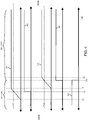
- FIG. 4 is an example timing diagram illustrating input voltage control during ramp-up of multiple power supplies according to embodiments herein.
- the controller 140 controls connectivity (such as via one or more switches associated with S1) of the first circuit path 101 to the second circuit path 102 as a function of the first input voltage 131 and the second input voltage 132 during ramp up of either or both of the first input voltage 131 and the second input voltage 132.
- connectivity such as via one or more switches associated with S1
- the controller 140 controls connectivity (such as via one or more switches associated with S1) of the first circuit path 101 to the second circuit path 102 as a function of the first input voltage 131 and the second input voltage 132 during ramp up of either or both of the first input voltage 131 and the second input voltage 132.
- Such embodiments ensure that a same input voltage level is applied to the first circuit path 101 (and input 141) and the second circuit path 102 (and input 142) during startup of the power supplies 121 and 122.
- the controller 140 monitors both a magnitude of the first input voltage 131 and a magnitude of the second input voltage 132 during a startup (ramping up) condition of the first power supply 121 producing the first input voltage 131 and the second power supply 122 producing the second input voltage 132.
- the controller 140 activates the switch S1. Because the switch S1 is ON, the input voltage 131 supplies power via input voltage 131 to both the first input 141 and the second input 142 of the load 118. In other words, via switch S1, the input voltage 131 is conveyed to the second input 142 of the load 118.
- the input voltage 131 is below the threshold value TV1. In such an instance, the load 118 is not properly powered. However, between time T2 and time T4, the input voltage 131 is above the threshold value TV1. In such an instance, the load 118 and corresponding input 141 and input 142 are powered with a single input voltage 131. In one embodiment, the input voltage 131 allows the load 118 to operate in at least a sleep mode or a low power mode as the power supply 121 may not be able to supply sufficient current for the load 118 to operate in a maximum power consumption mode.
- a magnitude of the input voltage 132 also increases above the threshold value TV2.
- the controller 140 deactivates the switch S1; the power supply 121 supplies power to the first input 141 of the load 118 independent of the power supply 122 supplying input voltage 132 to the second input 142 of the load 118.
- the load 118 is able to operate in a maximum power consumption mode because both input voltage 141 and input voltage 142 supply current to the dynamic load 118.
- the monitor signal 162 switches to a logic low. This causes the controller 140 to activate the switch S1 to an ON state.
- the controller 140 activates the switch S1. Because the switch S1 is ON, the input voltage 131 supplies power via input voltage 131 to both the first input 141 and the second input 142 of the load 118. In other words, via switch S1, the input voltage 131 is conveyed to the second input 142 of the load 118.
- the input voltage 131 is below the threshold value TV1. In such an instance, the load 118 is not properly powered. However, between time T7 and time T9, the input voltage 131 is above the threshold value TV1. In such an instance, the load 118 is powered with a single input voltage 131. In one embodiment, the input voltage 131 allows the load 118 to operate in at least a sleep mode or low power consumption to the limit of power supply 121 supplying current via input voltage 131.
- FIG. 6 is an example diagram illustrating switch circuitry according to embodiments herein.
- the apparatus such as power system 100
- switch S1 as described herein include one or more field effect transistors (switches).
- the series combination of switch Q2 and switch Q6 are coupled between node A and node B of switch S1.
- the drain node (D) of switch Q2 is connected to node A; the drain node (D) of switch Q6 is connected to node B; the source node (S) of switch Q2 is connected to the source node (S) of switch Q6; each of the gate node (G) of switch Q2 and the gate node (G) of switch Q6 are connected to node C.
- the series combination of switch Q3 and switch Q7 are coupled between node A and node B of switch S1.
- the drain node (D) of switch Q3 is connected to node A; the drain node (D) of switch Q7 is connected to node B; the source node (S) of switch Q3 is connected to the source node (S) of switch Q7; each of the gate node (G) of switch Q3 and the gate node (G) of switch Q7 are connected to node C.
- switch Q4 and switch Q8 are coupled between node A and node B of switch S1.
- the drain node (D) of switch Q4 is connected to node A; the drain node (D) of switch Q8 is connected to node B; the source node (S) of switch Q4 is connected to the source node (S) of switch Q8; each of the gate node (G) of switch Q4 and the gate node (G) of switch Q8 are connected to node C.
- the controller 140 generates the signal 105 as a logic high voltage (such as greater than 1VDC) to turn ON the switch S1 and corresponding field effect transistors, connecting the node A and node B.
- the controller 140 generates the signal 105 as a logic high low (such as around 0 VDC) to turn OFF the switch S1 and corresponding field effect transistors, disconnecting the node A and node B.
- FIG. 7 is an example diagram illustrating switch circuitry according to embodiments herein.
- the switch S1 includes switches Q1, Q2, Q3, and Q4 disposed in parallel between node A and node B.
- the drain node (D) of switch Q1 is connected to node A of switch S1; the source node (S) of switch Q1 is connected to node B of switch S1; the gate node (G) of switch Q1 is connected to node C of switch S1.
- the drain node (D) of switch Q2 is connected to node A of switch S1; the source node (S) of switch Q2 is connected to node B of switch S1; the gate node (G) of switch Q2 is connected to node C of switch S1.
- the drain node (D) of switch Q3 is connected to node A of switch S1; the source node (S) of switch Q3 is connected to node B of switch S1; the gate node (G) of switch Q3 is connected to node C of switch S1.
- the drain node (D) of switch Q4 is connected to node A of switch S1; the source node (S) of switch Q4 is connected to node B of switch S1; the gate node (G) of switch Q4 is connected to node C of switch S1.
- the controller 140 generates the signal 105 as a logic high voltage (such as greater than 1VDC) to turn ON the switch S1 and corresponding field effect transistors, connecting the node A and node B.
- the controller 140 generates the signal 105 as a logic high low (such as around 0 VDC) to turn OFF the switch S1 and corresponding field effect transistors, disconnecting the node A and node B.
- FIG. 8 is an example diagram illustrating switch circuitry according to embodiments herein.
- the switch S1 includes switches Q5, Q6, Q7, and Q8 disposed in parallel between node A and node B.
- the source node (S) of switch Q5 is connected to node A of switch S1; the drain node (D) of switch Q5 is connected to node B of switch S1; the gate node (G) of switch Q5 is connected to node C of switch S1.
- the source node (S) of switch Q6 is connected to node A of switch S1; the drain node (D) of switch Q6 is connected to node B of switch S1; the gate node (G) of switch Q6 is connected to node C of switch S1.
- the source node (S) of switch Q7 is connected to node A of switch S1; the drain node (D) of switch Q7 is connected to node B of switch S1; the gate node (G) of switch Q7 is connected to node C of switch S1.
- the source node (S) of switch Q8 is connected to node A of switch S1; the drain node (D) of switch Q8 is connected to node B of switch S1; the gate node (G) of switch Q8 is connected to node C of switch S1.
- the controller 140 In a manner as previously discussed, the controller 140 generates the signal 105 as a logic high voltage (such as greater than 1VDC) to turn ON the switch S1, connecting the node A and node B.
- the controller 140 generates the signal 105 as a logic high low (such as around 0 VDC) to turn OFF the switch S1, disconnecting the node A and node B.
- FIG. 9 is an example diagram illustrating switch circuitry according to embodiments herein. Still further embodiments of the apparatus (such as power system 100) as described herein include one or more field effect transistors (switches).
- the switch S1 includes multiple switches such as switch Q1, switch Q2, switch Q3, switch Q4, switch Q5, switch Q6 , switch Q7 and switch Q8.
- the switch S1 can include any number of switches.
- the series combination of switch Q1 and switch Q5 are coupled between node A and node B of switch S1.
- the source node (S) of switch Q1 is connected to node A; the source node (S) of switch Q5 is connected to node B; the drain node (D) of switch Q1 is connected to the drain node (D) of switch Q5; each of the gate node (G) of switch Q1 and the gate node (G) of switch Q5 are connected to node C.
- switch Q2 and switch Q6 are coupled between node A and node B of switch S1.
- the source node (S) of switch Q2 is connected to node A; the source node (S) of switch Q6 is connected to node B; the drain node (D) of switch Q2 is connected to the drain node (D) of switch Q6; each of the gate node (G) of switch Q2 and the gate node (G) of switch Q6 are connected to node C.
- the series combination of switch Q3 and switch Q7 are coupled between node A and node B of switch S1.
- the source node (S) of switch Q3 is connected to node A; the source node (S) of switch Q7 is connected to node B; the drain node (D) of switch Q3 is connected to the drain node (D) of switch Q7; each of the gate node (G) of switch Q3 and the gate node (G) of switch Q7 are connected to node C.
- switch Q4 and switch Q8 are coupled between node A and node B of switch S1.
- the source node (S) of switch Q4 is connected to node A; the source node (S) of switch Q8 is connected to node B; the drain node (D) of switch Q4 is connected to the drain node (D) of switch Q8; each of the gate node (G) of switch Q4 and the gate node (G) of switch Q8 are connected to node C.
- the controller 140 In a manner as previously discussed, the controller 140 generates the signal 105 as a logic high voltage (such as greater than 1VDC) to turn ON the switch S1, connecting the node A and node B.
- the controller 140 generates the signal 105 as a logic high low (such as around 0 VDC) to turn OFF the switch S1, disconnecting the node A and node B.
- the load 118 as described herein can be configured to consume a high amount of current, requiring power from multiple different power supplies.
- embodiments herein include implementing supplemental switch circuitry S1 (such as via one or more switches) to ensure that different portions of circuitry in the load 118 are powered at the same time with a same input voltage magnitude even though the power supplies (such as power converters) asynchronously generate the input voltages 131 and 132.
- the controller 140 temporarily connects the input voltages 131 and 132 from different power sources to ensure simultaneous powering of the load 118 with one of the input voltages until both power supplies 121 and 122 produce input voltages 131 and 132 to be above one or more threshold values.
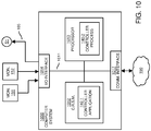
- FIG. 10 is an example block diagram of a computer device for implementing any of the operations as discussed herein according to embodiments herein.
- computer system 1000 (such as implemented by any of one or more resources such as controller 140, monitor 151, monitor 152, power supply 121, power supply 122, etc.) of the present example includes an interconnect 1011 that couples computer readable storage media 1012 such as a non-transitory type of media (or hardware storage media) in which digital information can be stored and retrieved, a processor 1013 (e.g., computer processor hardware such as one or more processor devices), I/O interface 1014, and a communications interface 1017.
- computer readable storage media 1012 such as a non-transitory type of media (or hardware storage media) in which digital information can be stored and retrieved
- processor 1013 e.g., computer processor hardware such as one or more processor devices
- I/O interface 1014 e.g., I/O interface 1014
- Computer readable storage medium 1012 can be any hardware storage resource or device such as memory, optical storage, hard drive, floppy disk, etc. In one embodiment, the computer readable storage medium 1012 stores instructions and/or data used by the control application 140-1 to perform any of the operations as described herein.
- communications interface 1017 enables the computer system 1000 and processor 1013 to communicate over a resource such as network 190 to retrieve information from remote sources and communicate with other computers.
- control application 140-1 e.g., software, firmware, etc.
- processor 1013 executes instructions to implement any of the operations as discussed herein.
- processor 1013 accesses computer readable storage media 1012 via the use of interconnect 1011 in order to launch, run, execute, interpret or otherwise perform the instructions in control application 140-1 stored on computer readable storage medium 1012.
- control application 140-1 produces processing functionality such as control process 140-2 in processor 1013.
- control process 140-2 associated with processor 1013 represents one or more aspects of executing control application 140-1 within or upon the processor 1013 in the computer system 1000.
- computer system 1000 can be a micro-controller device, logic, hardware processor, hybrid analog/digital circuitry, etc., configured to control a power supply and perform any of the operations as described herein.
- FIG. 11 is an example diagram illustrating a method of controlling a power supply according to embodiments herein.
- the controller 140 monitors a first input voltage 131 (VIN1) supplied by power supply 121 to power a first input (such as one or more input voltage pins 141) of a load 118 over a first circuit path 101.
- VIN1 first input voltage 131
- the controller 140 monitors a second input voltage 132 (VIN2) supplied by power supply 122 to power a second input (such as one or more input voltage pins) of the load 118 over a second circuit path 102.
- VIN2 a second input voltage 132 supplied by power supply 122 to power a second input (such as one or more input voltage pins) of the load 118 over a second circuit path 102.
- the controller 140 controls connectivity of the first circuit path 101 and the second circuit path 102 to each other as a function of the first input voltage 131 and the second input voltage 132.
- FIG. 12 is an example diagram illustrating assembly of a power supply circuit on a circuit board according to embodiments herein.
- assembler 1240 receives a substrate 1210 (such as a circuit board).
- the assembler 1240 further affixes (couples) the controller 140 (and one or more corresponding components or system such as power supply 121, power supply 122, monitor 151, monitor, etc., associated with the power system 100) to the substrate 1210.
- the assembler 1240 couples the controller 140 and corresponding resources as shown in FIG. 1 .
- components such as the controller 140, power supply 121, power supply 122, monitor 151, monitor 152, etc., associated with the power system 100 can be affixed or coupled to the substrate 1210 in any suitable manner.
- one or more of the components in power supply 100 can be soldered to the substrate, inserted into sockets on the substrate 1210, etc.
- Circuit paths may be disposed in cables providing connectivity between the power system 100 and the load 118.
- the load 118 is disposed on its own substrate independent of substrate 1210; the substrate of the load 118 is directly or indirectly connected to the substrate 1210, etc.
- the controller 140 or any portion of the power system 100 can be disposed on a standalone smaller board plugged into a socket of the substrate 1210.
- embodiments herein include a system comprising: a substrate 1210 (such as a circuit board, standalone board, mother board, standalone board destined to be coupled to a mother board, host, etc.); a power system 100 including corresponding components as described herein; and a load 118.
- the load 118 is powered based on conveyance of the input voltage 131 and/or input voltage 132 conveyed over one or more circuit paths 101 and 102 to the load 118.
- An algorithm as described herein, and generally, is considered to be a self-consistent sequence of operations or similar processing leading to a desired result.
- operations or processing involve physical manipulation of physical quantities.
- quantities may take the form of electrical or magnetic signals capable of being stored, transferred, combined, compared or otherwise manipulated. It has been convenient at times, principally for reasons of common usage, to refer to such signals as bits, data, values, elements, symbols, characters, terms, numbers, numerals or the like. It should be understood, however, that all of these and similar terms are to be associated with appropriate physical quantities and are merely convenient labels.
Landscapes
- Engineering & Computer Science (AREA)
- Power Engineering (AREA)
- Physics & Mathematics (AREA)
- General Physics & Mathematics (AREA)
- Theoretical Computer Science (AREA)
- General Engineering & Computer Science (AREA)
- Automation & Control Theory (AREA)
- Electromagnetism (AREA)
- Radar, Positioning & Navigation (AREA)
- Microelectronics & Electronic Packaging (AREA)
- Electronic Switches (AREA)
- Direct Current Feeding And Distribution (AREA)
- Power Sources (AREA)
Abstract
Description
- As a result of the ever-increasing need for more processing power and ethernet data traffic, newer circuits such as Ethernet ASICs (Application Specific Integrated Circuits) now require more complex power delivery requirements.
- For example, the general trend is toward increasing load current with lower core voltages. In certain instances, a load such as a circuit has a core voltage requirement of 0.75V and up to 2400 Amperes.
- Currently, there is no single controller capable of simultaneously driving a sufficient number of power converter phases to deliver appropriate power (such as via 2400 Amperes) to power the load. This means that conventional power supply technology may require two separate asynchronous power converters to supply power to the load.
- This disclosure includes the observation that conventional power supply monitoring and power supply control techniques suffer from deficiencies. For example, it is not desirable to supply different levels of input voltages from asynchronous power supplies to different input voltage pins of a load as such different input voltage levels may cause damage to a corresponding load.
- Embodiments herein include novel ways of tracking and controlling power delivery in a multi-phase power supply simultaneously supplying power to a common load.
- More specifically, embodiments herein include an apparatus comprising a first power supply, a second power supply, and a controller. The first power supply supplies a first input voltage to power a first input of a load over a first circuit path. The second power supply supplies a second input voltage to power a second input of the load over a second circuit path. During operation, to ensure simultaneous application of a same input voltage level to input voltage pins of the load from the different power supplies (such as first power supply and second power supply), the controller controls connectivity of the first circuit path to the second circuit path as a function of the first input voltage and the second input voltage.
- In one embodiment, the controller controls connectivity (such as via one or more switches) of the first circuit path to the second circuit path as a function of the first input voltage and the second input voltage during ramp up or ramp down of either or both of the first input voltage and the second input voltage. Such embodiments ensure that a same input voltage level is applied to the first circuit path and the second circuit path during startup and shut down of the power supplies.
- Further embodiments herein include switch circuitry connected between the first circuit path and the second circuit path. The controller controls activation of the switch circuitry to an ON state during ramping of the first input voltage from the first power supply. Ramping occurs at startup of generating the respective first input voltage and the second input voltage. Ramping also occurs at power down of discontinuing generation of the respective first input voltage and the second input voltage.
- In yet further example embodiments, the apparatus as described herein includes switch circuitry (such as one or more switches) connected between the first circuit path and the second circuit path. The controller controls activation of the switch circuitry to an ON state in response to detecting a condition in which a magnitude of the first input voltage is below a first threshold voltage value and a magnitude of the second voltage is below a second threshold voltage value. This ensures that a same voltage is applied to the load at different inputs (such as pins, ports, etc.)
- In still further example embodiments, the controller monitors both a magnitude of the first input voltage and a magnitude of the second input voltage during a startup (ramping up) condition of the first power supply producing the first input voltage and the second power supply producing the second input voltage. Depending on detected operating conditions, the controller switches between connecting the first circuit path and the second circuit path and disconnecting the first circuit path from the second circuit path.
- For example, in one embodiment, the controller electrically connects the first circuit path and the second circuit path to each other via a low impedance (such as short circuit) path prior to both the first power supply producing the first input voltage above a first threshold value and the second power supply producing the second input voltage above a second threshold value.
- Alternatively, in one embodiment, the controller disconnects (provides an open circuit) the first circuit path and the second circuit path subsequent to both the first power supply producing the first input voltage above a first threshold voltage value and the second power supply producing the second input voltage above a second threshold voltage value.
- In still further example embodiments, generation of the first input voltage by the first power supply is asynchronous with respect to generation of the second input voltage by the second power supply. More specifically, in one embodiment, the first power supply (such as one or more power supply phases) operates off a different signal clock than the second power supply (such as one or more power supply phases). Control as described herein supports simultaneous input of an input voltage to the load at different inputs even though one of the power supplies may be slower to produce an input voltage to power the load.
- In still further example embodiments, the load includes a first input such as first input pins and second input such as second input pins, each of which is configured to receive an input voltage to power different internal circuitry in the load. In one embodiment, the first input includes a first set of multiple input voltage pins, each of which supplies power (via the first input voltage) to a first portion (first circuitry) of the load; and the second input includes a second set of multiple input voltage pins, each of which supplies power (via the second input voltage) to a second portion (first circuitry) of the load. In one embodiment, during power up of the first circuitry and the second circuitry, the first circuitry interacts w the second circuitry.
- Further embodiments herein include, via the controller, providing an electrically conductive path between the first circuit path and the second circuit path prior to both or either of the first input voltage being above a first threshold value and the second input voltage being above a second threshold value.
- Still further embodiments of the apparatus (or system, device, hardware, etc.) as described herein include one or more field effect transistors (switches). In one embodiment, a field effect transistor directly couples the first circuit path and the second circuit path. The controller controls a state of the field effect transistor as a function of a magnitude of the first input voltage and a magnitude of the second input voltage.
- Yet further example embodiments herein include a first switch coupled in series with a second switch between the first circuit path and the second circuit path. The switch includes any number of series switches connected in parallel. The controller produces a common control signal that simultaneously controls both the first switch circuitry and the second switch circuitry to an OFF state subsequent to detecting that both a magnitude of the first input voltage and the second input voltage are above a threshold value. Conversely, the controller produces the common control signal to simultaneously control both the first switch circuitry and the second switch circuitry to an OFF state in response to detecting that both a magnitude of the first input voltage and the second input voltage are above a voltage threshold value. Such an embodiment prevents the power supply outputs from being shorted to each other when they are both up and running.
- Accordingly, embodiments herein include providing connectivity between the first circuit path and the second circuit path during ramping of the first power supply and the second power supply. After the first input voltage and the second input voltage are above respective threshold values, the controller electrically disconnects the first circuit path and the second circuit path.
- Embodiments herein are beneficial over conventional techniques. For example, the load as described herein can be configured to consume a high amount of current; requiring power from multiple different power supply sources. Instead of implementing complex circuitry to synchronize generation and application of an input voltage from each of multiple sources to different portions of circuitry in a load to ensure mirroring of the input voltages from multiple different power supplies, embodiments herein include implementing supplemental switch circuitry (one or more switches) to ensure that different portions of circuitry in the load are powered at the same time with a same input voltage magnitude even though the power supplies asynchronously generate the input voltages. In other words, during power up and power down of both power supplies and powering the different portions of load, the controller controls the switch circuitry temporarily connects the input voltages from different power supply sources to ensure simultaneous powering until both power supplies produce receive input voltages applied to the load above a threshold value.
- These and other more specific embodiments are disclosed in more detail below.
- Note that although embodiments as discussed herein are applicable to power supplies and powering a respective load, the concepts disclosed herein may be advantageously applied to any other suitable topologies as well as general power supply control applications.
- Note that any of the resources as discussed herein can include one or more computerized devices, mobile communication devices, servers, base stations, wireless communication equipment, communication management systems, workstations, user equipment, handheld or laptop computers, or the like to carry out and/or support any or all of the method operations disclosed herein. In other words, one or more computerized devices or processors can be programmed and/or configured to operate as explained herein to carry out the different embodiments as described herein.
- Yet other embodiments herein include software programs to perform the steps and operations summarized above and disclosed in detail below. One such embodiment comprises a computer program product including a non-transitory computer-readable storage medium (i.e., any computer readable hardware storage medium) on which software instructions are encoded for subsequent execution. The instructions, when executed in a computerized device (hardware) having a processor, program and/or cause the processor (hardware) to perform the operations disclosed herein. Such arrangements are typically provided as software, code, instructions, and/or other data (e.g., data structures) arranged or encoded on a non-transitory computer readable storage medium such as an optical medium (e.g., CD-ROM), floppy disk, hard disk, memory stick, memory device, etc., or other a medium such as firmware in one or more ROM, RAM, PROM, etc., or as an Application Specific Integrated Circuit (ASIC), etc. The software or firmware or other such configurations can be installed onto a computerized device to cause the computerized device to perform the techniques explained herein.
- Accordingly, embodiments herein are directed to methods, systems, computer program products, etc., that support operations as discussed herein.
- One embodiment herein includes a computer readable storage medium and/or system having instructions stored thereon. The instructions, when executed by computer processor hardware, cause the computer processor hardware (such as one or more co-located or disparately located processor devices) to: monitor a first input voltage supplied to power a first input of a load over a first circuit path; monitor a second input voltage supplied to power a second input of the load over a second circuit path; and control connectivity of the first circuit path and the second circuit path to each other as a function of the first input voltage and the second input voltage.
- The ordering of the steps above has been added for clarity sake. Note that any of the processing steps as discussed herein can be performed in any suitable order.
- Other embodiments of the present disclosure include software programs and/or respective hardware to perform any of the method embodiment steps and operations summarized above and disclosed in detail below.
- It is to be understood that the system, method, apparatus, instructions on computer readable storage media, etc., as discussed herein also can be embodied strictly as a software program, firmware, as a hybrid of software, hardware and/or firmware, or as hardware alone such as within a processor (hardware or software), or within an operating system or a within a software application.
- As discussed herein, techniques herein are well suited for use in the field of supporting switching power supplies. However, it should be noted that embodiments herein are not limited to use in such applications and that the techniques discussed herein are well suited for other applications as well.
- Additionally, note that although each of the different features, techniques, configurations, etc., herein may be discussed in different places of this disclosure, it is intended, where suitable, that each of the concepts can optionally be executed independently of each other or in combination with each other. Accordingly, the one or more present inventions as described herein can be embodied and viewed in many different ways.
- Also, note that this preliminary discussion of embodiments herein (BRIEF DESCRIPTION OF EMBODIMENTS) purposefully does not specify every embodiment and/or incrementally novel aspect of the present disclosure or claimed invention(s). Instead, this brief description only presents general embodiments and corresponding points of novelty over conventional techniques. For additional details and/or possible perspectives (permutations) of the invention(s), the reader is directed to the Detailed Description section (which is a summary of embodiments) and corresponding figures of the present disclosure as further discussed below.
-
FIG. 1 is an example general diagram of a power supply system supporting input and control of different input voltages to a load according to embodiments herein. -
FIG. 2 is an example detailed diagram of a power supply system supporting input and control of different input voltages to a load according to embodiments herein. -
FIG. 3 is an example diagram illustrating a truth table of controlling connectivity of multiple circuit paths according to embodiments herein. -
FIG. 4 is an example timing diagram of multiple ramping up power supplies and corresponding control of switch connectivity according to embodiments herein. -
FIG. 5 is an example timing diagram of multiple ramping down power supplies and corresponding control of switch connectivity according to embodiments herein. -
FIG. 6 is an example diagram illustrating switch circuitry according to embodiments herein. -
FIG. 7 is an example diagram illustrating switch circuitry according to embodiments herein. -
FIG. 8 is an example diagram illustrating switch circuitry according to embodiments herein. -
FIG. 9 is an example diagram illustrating switch circuitry according to embodiments herein. -
FIG. 10 is an example diagram illustrating computer processor hardware and related software instructions that execute methods according to embodiments herein. -
FIG. 11 is an example diagram illustrating a method according to embodiments herein. -
FIG. 12 is an example diagram illustrating fabrication of a circuit according to embodiments herein. - The foregoing and other objects, features, and advantages of the invention will be apparent from the following more particular description of preferred embodiments herein, as illustrated in the accompanying drawings in which like reference characters refer to the same parts throughout the different views. The drawings are not necessarily to scale, with emphasis instead being placed upon illustrating the embodiments, principles, concepts, etc.
- Embodiments herein include an apparatus comprising multiple power supplies and a controller. In one embodiment, the multiple power supplies include a first power supply and a second power supply. During operation, the first power supply supplies a first input voltage over a first circuit path to power a first input of a load. The second power supply supplies a second input voltage over a second circuit path to power a second input of the load. The controller controls connectivity of the first circuit path to the second circuit path as a function of the first input voltage and the second input voltage during at least ramp up or ramp down of either or both of the first input voltage and the second input voltage. For example, as further discussed herein, during both ramp-up and ramp down of the first input voltage and the second input voltage, the controller electrically connects the first circuit path and the second circuit path prior to detecting that both the first input voltage and the second input voltage are above a respective threshold value.
- Such embodiments ensure that different inputs (such as different sets of input voltage pins of a load) simultaneously receive the same input voltage during both ramp-up and ramp down of the power supplies.
- Now, more specifically,
FIG. 1 is an example general diagram of a power supply supporting generation and input of different input voltages to a load according to embodiments herein. In this example embodiment, thepower system 100 includespower supply 121power supply 122, monitor 151, monitor 152,controller 140, switch S1, andload 118. - The
load 118 includes any number of inputs to receive power such as multiple input voltages. - For example, in this example embodiment, the
load 118 includes afirst input 141 such as one or more input voltage pins; theload 118 includes asecond input 142 such as one or more input voltage pins. -
Load 118 can be configured to include any number inputs to receive respective input voltages. For illustrative sake, theload 118 inFIG. 1 includes two inputs, namely,input 141 andinput 142. - As further shown, the
power supply 121 produces the input voltage 131 (such as VIN1). Thepower supply 121 outputs theinput voltage 131 to thecircuit path 101.Circuit path 101 conveys theinput voltage 131 from thepower supply 121 to theinput 141 of theload 118 as well as the node A of switch S1. - Additionally, the
power supply 122 produces the input voltage 132 (such as VIN2). Thepower supply 122 outputs theinput voltage 132 to thecircuit path 102.Circuit path 102 conveys theinput voltage 132 from thepower supply 122 to theinput 142 of theload 118 as well as the node B of switch S1. - The state of switch S1 controls an open circuit or short circuit condition between node A and node B of switch S1.
- As previously discussed, the
power system 100 as described herein further includes monitor 151 and monitor 152. As shown, themonitor 151 monitors theinput voltage 131 supplied by thepower supply 121 to theinput 141 of theload 118. In one embodiment, themonitor 151 compares the magnitude of theinput voltage 131 to a respective threshold value TV1. Based upon a comparison of the magnitude of theinput voltage 131 to the respective threshold value TV1, themonitor 151 produces themonitor signal 161. Themonitor 151 outputs themonitor signal 161 to thecontroller 140. In one embodiment, themonitor signal 161 indicates whether or not theinput voltage 131 is greater than or less than the threshold value TV1. - In a similar manner, the
monitor 152 monitors theinput voltage 132 supplied by thepower supply 122 to theinput 142 of theload 118. In one embodiment, themonitor 152 compares the magnitude of theinput voltage 132 to a respective threshold value TV2. Based upon a comparison of the magnitude of theinput voltage 132 to the respective threshold value TV2, themonitor 152 produces and outputs themonitor signal 162 to thecontroller 140. In one embodiment, themonitor signal 162 indicates whether or not theinput voltage 132 is greater than or less than the threshold value TV2. - As previously discussed, embodiments herein include novel ways of monitoring and controlling simultaneous power delivery from multiple power supplies to a
load 118. For example, in one embodiment, thecontroller 140 monitors the receivedmonitor signal 161 and monitorsignal 162. To ensure simultaneous application of the same input voltage level to bothinput first circuit path 101 to thesecond circuit path 102 as a function of thefirst input voltage 131 and thesecond input voltage 132. - In one embodiment, the
first power supply 121 and thesecond power supply 122 operate asynchronously with respect to each other. For example, in one nonlimiting example embodiment, thepower supply 121 operates off of a first clock (Clock1); thepower supply 122 operates off of a second clock (Clock2). - Additionally, or alternatively, the
power supply 121 andpower supply 122 operate off the same clock input. However, the power supplies produce therespective input voltages respective input voltage 131 is not always equal to the magnitude of theinput voltage 132 on power up and power down. In one embodiment, when both theinput voltage 131 in theinput voltage 132 are above a threshold value, it is desirable to disconnect thecircuit path 101 from thecircuit path 102. - In this example embodiment, controlling connectivity of the
first circuit path 101 and thesecond circuit path 102 includes controlling a respective state of the switch S1. - More specifically, as further discussed herein, in response to detecting that the
input voltage 131 is less than the threshold value TV1 or detecting that theinput voltage 132 is less than the threshold value TV2, thecontroller 140 controls the switch to an ON state, providing a low impedance path (short circuit path) between thefirst circuit path 101 and thesecond circuit path 102. - As previously discussed, in response to detecting a condition in which both the
input voltage 131 is greater than the threshold value TV1 and theinput voltage 132 is greater than the threshold value TV2, thecontroller 140 controls the switch S1 to an OFF state, providing a high impedance path (open circuit path) between thefirst circuit path 101 and thesecond circuit path 102. -
FIG. 2 is an example diagram illustrating a controller and corresponding switch circuitry according to embodiments herein. In this example embodiment, thepower supply 121 includes a multiphase controller PC1 and corresponding multiple phases PH11, PH 12, etc. In response to receiving a respective ENABLE signal indicating to generate arespective input voltage 131, the multiphase controller PC1 controls operation of the multiple phases PH11, PH12, etc., to convert a power supply voltage into the respective input voltage 131 (such as 1.0 VDC or other suitable value) supplied to node A of the switch S1 and theinput 141. - In one embodiment, the
power supply 121 includes thirty-two phases (such as offset phase) that produce therespective input voltage 131. However, thepower supply 121 can include any number of phases. - Further in this example embodiment, the
power supply 122 includes a multiphase controller PC2 and corresponding multiple phases PH21, PH22, etc. In response to receiving a respective ENABLE signal indicating to generate arespective input voltage 132, the multiphase controller PC2 controls operation of the multiple phases PH21, PH22, etc., to convert a received power supply voltage into the respective input voltage 132 (such as 1.0VDC or other suitable value) supplied to node B of the switch S1 and theinput 142. - In one embodiment, the
power supply 122 includes thirty-two phases (such as offset phases) that produce therespective input voltage 132. However, thepower supply 122 can include any number of phases. - As further shown in this example embodiment, the
controller 140 includes arespective NAND gate 220 as well as driver D1 controlling operation of the switch S1 via driving node C with thecontrol signal 105. The NAND produces control signal 205 based upon respective states ofmonitor signal 161 and monitorsignal 162. - Driver D1 produces the respective control signal 105 to drive node C depending upon the state of the
control signal 205 generated by theNAND gate 220. Additional details of generating therespective control signal 205 andcontrol signal 105 and corresponding truth table 310 are shown inFIG. 3 . - Referring again to
FIG. 2 , as previously discussed, theload 118 includes afirst input 141 such as first one or more input pins andsecond input 142 such as second one or more input pins, each of which is configured to receive an input voltage to power circuitry in the load. - More specifically, the
load 118 includesinput 141 to receive theinput voltage 131 generated by thepower supply 121. Viainput 141, theinput voltage 131 powers the first portion 251 (such as first circuitry) of theload 118. Theload 118 includesinput 142 to receive theinput voltage 132 generated by thepower supply 122. Viainput 142, theinput voltage 132 powers the second portion 252 (such as second circuitry) of theload 118. - In one embodiment, the load is a single integrated circuit. Alternatively, the
load 118 can include any number of integrated circuits. - As previously discussed, in one embodiment, even though the
inputs load 118 are coupled to different circuitry, it is desirable that the same voltage is applied to thedifferent inputs respective input voltages - Accordingly, in one embodiment, the
first input 141 includes a first set of multiple input voltage pins, which collectively supply power (via the first input voltage 131) to a first portion 251 (first set of load circuitry) of theload 118; and thesecond input 142 includes a second set of multiple input voltage pins, which collectively supply power (via the second input voltage 132) to a second portion 252 (second set of load circuitry) of theload 118. -
FIG. 3 is an example diagram illustrating different operational states of controlling connectivity of multiple input voltage paths according to embodiments herein. As previously discussed, thecontroller 140 monitors the magnitude of therespective input voltage 131 viamonitor signal 161; thecontroller 140 monitors the magnitude of therespective input voltage 132 viamonitor signal 162. - In one embodiment, via the NAND control function supplied by the
NAND gate 220, and as indicated by the truth table 310, thecontroller 140 activates the switch S1 to an ON state (short circuit ofcircuit path 101 and circuit path 102) in response to detecting that themonitor signal 161 is logic low (corresponding to a condition in which the magnitude of theinput voltage 131 is below the threshold value TV1) and monitorsignal 162 is logic low (corresponding to a condition in which the magnitude of theinput voltage 132 is below the threshold value TV2). - Via the NAND control function supplied by the
NAND gate 220, and as indicated by the truth table 310, thecontroller 140 activates the switch S1 to an ON state (short circuit ofcircuit path 101 and circuit path 102) in response to detecting that themonitor signal 161 is logic low (corresponding to a condition in which the magnitude of theinput voltage 131 is below the threshold value TV1) and monitorsignal 162 is logic high (corresponding to a condition in which the magnitude of theinput voltage 132 is above the threshold value TV2). - Via the NAND control function supplied by the
NAND gate 220, and as indicated by the truth table 310, thecontroller 140 activates the switch S1 to an ON state (short circuit ofcircuit path 101 and circuit path 102) in response to detecting that themonitor signal 161 is logic high (corresponding to a condition in which the magnitude of theinput voltage 131 is above the threshold value TV1) and monitorsignal 162 is logic low (corresponding to a condition in which the magnitude of theinput voltage 132 is below the threshold value TV2). - Activation of the respective switch S1 for the above 3 states (00, 01, and 10) ensures that a same voltage is applied to the
load 118 at thedifferent inputs 141 and 142 (such as pins, ports, etc.) when either or both of the input voltages are below a respective threshold value. - Via the NAND control function supplied by the
NAND gate 220, and as indicated by the truth table 310, thecontroller 140 deactivates the switch S1 to an OFF state (open circuit betweencircuit path 101 and circuit path 102) in response to detecting that themonitor signal 161 is logic high (corresponding to a condition in which the magnitude of theinput voltage 131 is above the threshold value TV1) and monitorsignal 162 is logic high (corresponding to a condition in which the magnitude of theinput voltage 132 is above the threshold value TV2). - Deactivation of the respective switch S1 for the final state (11) ensures that the outputs of the power supplies 121 and 122 are not shorted to each other (i.e.,
circuit path 101 is not connected to circuit path 102) during a condition in which their respective magnitudes are above the operating threshold values TV1 and TV2. - Note that the status of the
input voltages input voltage 131 may be above or below the threshold value TV1; theinput voltage 132 may be above or below the threshold value TV2. In accordance with the detected operating conditions (magnitudes ofinput voltages 131 and 132) as indicated by table 310, via switch S1 and corresponding control, thecontroller 140 switches between connecting thefirst circuit path 101 and thesecond circuit path 102 and disconnecting thefirst circuit path 101 and thesecond circuit path 102. -
FIG. 4 is an example timing diagram illustrating input voltage control during ramp-up of multiple power supplies according to embodiments herein. As shown in this example embodiment, thecontroller 140 controls connectivity (such as via one or more switches associated with S1) of thefirst circuit path 101 to thesecond circuit path 102 as a function of thefirst input voltage 131 and thesecond input voltage 132 during ramp up of either or both of thefirst input voltage 131 and thesecond input voltage 132. Such embodiments ensure that a same input voltage level is applied to the first circuit path 101 (and input 141) and the second circuit path 102 (and input 142) during startup of the power supplies 121 and 122. - For example, the
controller 140 monitors both a magnitude of thefirst input voltage 131 and a magnitude of thesecond input voltage 132 during a startup (ramping up) condition of thefirst power supply 121 producing thefirst input voltage 131 and thesecond power supply 122 producing thesecond input voltage 132. - Prior to time T1,
input voltage 131 is below the threshold value TV1;input voltage 132 is below the threshold value TV2. In such an instance, themonitor signal 161 and monitorsignal 162 are both a logic low. The logic low states cause thecontroller 140 to produce thecontrol signal 105 as a logic high, activating switch S1 to a short circuit (ON) state, connecting thecircuit path 101 to thecircuit path 102. - Between time T1 and time T4, the magnitude of the
input voltage 132 is below the threshold value TV2. This causes thecontroller 140 to activate the switch S1. Because the switch S1 is ON, theinput voltage 131 supplies power viainput voltage 131 to both thefirst input 141 and thesecond input 142 of theload 118. In other words, via switch S1, theinput voltage 131 is conveyed to thesecond input 142 of theload 118. - Note further that prior to time T2, the
input voltage 131 is below the threshold value TV1. In such an instance, theload 118 is not properly powered. However, between time T2 and time T4, theinput voltage 131 is above the threshold value TV1. In such an instance, theload 118 andcorresponding input 141 andinput 142 are powered with asingle input voltage 131. In one embodiment, theinput voltage 131 allows theload 118 to operate in at least a sleep mode or a low power mode as thepower supply 121 may not be able to supply sufficient current for theload 118 to operate in a maximum power consumption mode. - After time T4, a magnitude of the
input voltage 132 also increases above the threshold value TV2. In such an instance, thecontroller 140 deactivates the switch S1; thepower supply 121 supplies power to thefirst input 141 of theload 118 independent of thepower supply 122 supplyinginput voltage 132 to thesecond input 142 of theload 118. In such an instance, theload 118 is able to operate in a maximum power consumption mode because bothinput voltage 141 andinput voltage 142 supply current to thedynamic load 118. -
FIG. 5 is an example timing diagram illustrating input voltage control during ramp-down of multiple power supplies according to embodiments herein. As shown in this example embodiment, thecontroller 140 controls connectivity (such as via one or more switches associated with S1) of thefirst circuit path 101 to thesecond circuit path 102 as a function of thefirst input voltage 131 and thesecond input voltage 132 during ramp down of either or both of thefirst input voltage 131 and thesecond input voltage 132. Such embodiments ensure that a same input voltage level is applied to the first circuit path 101 (and input 141) and the second circuit path 102 (and input 142) during shut down of the power supplies 121 and 122. - For example, the
controller 140 monitors both a magnitude of thefirst input voltage 131 and a magnitude of thesecond input voltage 132 during a shut-down (ramping down) condition of thefirst power supply 121 producing thefirst input voltage 131 and thesecond power supply 122 producing thesecond input voltage 132. - Prior to time T7,
input voltage 131 is above the threshold value TV1;input voltage 132 is above the threshold value TV2. In such an instance, themonitor signal 161 and monitorsignal 162 are both a logic high. The logic high states cause thecontroller 140 to produce thecontrol signal 105 as a logic low, deactivating switch S1 to an open circuit (ON) state, disconnecting thecircuit path 101 from thecircuit path 102. - At time T7, the magnitude of the
input voltage 132 falls below the threshold value TV2. In such an instance, themonitor signal 162 switches to a logic low. This causes thecontroller 140 to activate the switch S1 to an ON state. - Thus, between time T7 and time T 10, the magnitude of the
input voltage 132 is below the threshold value TV2. This causes thecontroller 140 to activate the switch S1. Because the switch S1 is ON, theinput voltage 131 supplies power viainput voltage 131 to both thefirst input 141 and thesecond input 142 of theload 118. In other words, via switch S1, theinput voltage 131 is conveyed to thesecond input 142 of theload 118. - Note further that after time T9, the
input voltage 131 is below the threshold value TV1. In such an instance, theload 118 is not properly powered. However, between time T7 and time T9, theinput voltage 131 is above the threshold value TV1. In such an instance, theload 118 is powered with asingle input voltage 131. In one embodiment, theinput voltage 131 allows theload 118 to operate in at least a sleep mode or low power consumption to the limit ofpower supply 121 supplying current viainput voltage 131. -
FIG. 6 is an example diagram illustrating switch circuitry according to embodiments herein. In this example embodiment, the apparatus (such as power system 100) or switch S1 as described herein include one or more field effect transistors (switches). - For example, in this example embodiment, the switch S1 includes multiple switches such as switch Q1, switch Q2, switch Q3, switch Q4, switch Q 5, switch Q6 , switch Q7 and switch Q8. Note that the switch S1 can include any number of switches.
- As further shown, the series combination of switch Q1 and switch Q5 are coupled between node A and node B of switch S1. For example, the drain node (D) of switch Q1 is connected to node A; the drain node (D) of switch Q5 is connected to node B; the source node (S) of switch Q1 is connected to the source node (S) of switch Q5; each of the gate node (G) of switch Q1 and the gate node (G) of switch Q5 are connected to node C.
- In a similar manner, the series combination of switch Q2 and switch Q6 are coupled between node A and node B of switch S1. For example, the drain node (D) of switch Q2 is connected to node A; the drain node (D) of switch Q6 is connected to node B; the source node (S) of switch Q2 is connected to the source node (S) of switch Q6; each of the gate node (G) of switch Q2 and the gate node (G) of switch Q6 are connected to node C.
- In a similar manner, the series combination of switch Q3 and switch Q7 are coupled between node A and node B of switch S1. For example, the drain node (D) of switch Q3 is connected to node A; the drain node (D) of switch Q7 is connected to node B; the source node (S) of switch Q3 is connected to the source node (S) of switch Q7; each of the gate node (G) of switch Q3 and the gate node (G) of switch Q7 are connected to node C.
- In a similar manner, the series combination of switch Q4 and switch Q8 are coupled between node A and node B of switch S1. For example, the drain node (D) of switch Q4 is connected to node A; the drain node (D) of switch Q8 is connected to node B; the source node (S) of switch Q4 is connected to the source node (S) of switch Q8; each of the gate node (G) of switch Q4 and the gate node (G) of switch Q8 are connected to node C.
- In a manner as previously discussed, the
controller 140 generates thesignal 105 as a logic high voltage (such as greater than 1VDC) to turn ON the switch S1 and corresponding field effect transistors, connecting the node A and node B. Thecontroller 140 generates thesignal 105 as a logic high low (such as around 0 VDC) to turn OFF the switch S1 and corresponding field effect transistors, disconnecting the node A and node B. -
FIG. 7 is an example diagram illustrating switch circuitry according to embodiments herein. In this example embodiment, the switch S1 includes switches Q1, Q2, Q3, and Q4 disposed in parallel between node A and node B. For example, the drain node (D) of switch Q1 is connected to node A of switch S1; the source node (S) of switch Q1 is connected to node B of switch S1; the gate node (G) of switch Q1 is connected to node C of switch S1. - The drain node (D) of switch Q2 is connected to node A of switch S1; the source node (S) of switch Q2 is connected to node B of switch S1; the gate node (G) of switch Q2 is connected to node C of switch S1.
- The drain node (D) of switch Q3 is connected to node A of switch S1; the source node (S) of switch Q3 is connected to node B of switch S1; the gate node (G) of switch Q3 is connected to node C of switch S1.
- The drain node (D) of switch Q4 is connected to node A of switch S1; the source node (S) of switch Q4 is connected to node B of switch S1; the gate node (G) of switch Q4 is connected to node C of switch S1.
- In a manner as previously discussed, the
controller 140 generates thesignal 105 as a logic high voltage (such as greater than 1VDC) to turn ON the switch S1 and corresponding field effect transistors, connecting the node A and node B. Thecontroller 140 generates thesignal 105 as a logic high low (such as around 0 VDC) to turn OFF the switch S1 and corresponding field effect transistors, disconnecting the node A and node B. -
FIG. 8 is an example diagram illustrating switch circuitry according to embodiments herein. In this example embodiment, the switch S1 includes switches Q5, Q6, Q7, and Q8 disposed in parallel between node A and node B. - For example, the source node (S) of switch Q5 is connected to node A of switch S1; the drain node (D) of switch Q5 is connected to node B of switch S1; the gate node (G) of switch Q5 is connected to node C of switch S1.
- The source node (S) of switch Q6 is connected to node A of switch S1; the drain node (D) of switch Q6 is connected to node B of switch S1; the gate node (G) of switch Q6 is connected to node C of switch S1.
- The source node (S) of switch Q7 is connected to node A of switch S1; the drain node (D) of switch Q7 is connected to node B of switch S1; the gate node (G) of switch Q7 is connected to node C of switch S1.
- The source node (S) of switch Q8 is connected to node A of switch S1; the drain node (D) of switch Q8 is connected to node B of switch S1; the gate node (G) of switch Q8 is connected to node C of switch S1.
- In a manner as previously discussed, the
controller 140 generates thesignal 105 as a logic high voltage (such as greater than 1VDC) to turn ON the switch S1, connecting the node A and node B. Thecontroller 140 generates thesignal 105 as a logic high low (such as around 0 VDC) to turn OFF the switch S1, disconnecting the node A and node B. -
FIG. 9 is an example diagram illustrating switch circuitry according to embodiments herein. Still further embodiments of the apparatus (such as power system 100) as described herein include one or more field effect transistors (switches). - For example, in this example embodiment, the switch S1 includes multiple switches such as switch Q1, switch Q2, switch Q3, switch Q4, switch Q5, switch Q6 , switch Q7 and switch Q8. Note that the switch S1 can include any number of switches.
- As further shown, the series combination of switch Q1 and switch Q5 are coupled between node A and node B of switch S1. For example, the source node (S) of switch Q1 is connected to node A; the source node (S) of switch Q5 is connected to node B; the drain node (D) of switch Q1 is connected to the drain node (D) of switch Q5; each of the gate node (G) of switch Q1 and the gate node (G) of switch Q5 are connected to node C.
- In a similar manner, the series combination of switch Q2 and switch Q6 are coupled between node A and node B of switch S1. For example, the source node (S) of switch Q2 is connected to node A; the source node (S) of switch Q6 is connected to node B; the drain node (D) of switch Q2 is connected to the drain node (D) of switch Q6; each of the gate node (G) of switch Q2 and the gate node (G) of switch Q6 are connected to node C.
- In a similar manner, the series combination of switch Q3 and switch Q7 are coupled between node A and node B of switch S1. For example, the source node (S) of switch Q3 is connected to node A; the source node (S) of switch Q7 is connected to node B; the drain node (D) of switch Q3 is connected to the drain node (D) of switch Q7; each of the gate node (G) of switch Q3 and the gate node (G) of switch Q7 are connected to node C.
- In a similar manner, the series combination of switch Q4 and switch Q8 are coupled between node A and node B of switch S1. For example, the source node (S) of switch Q4 is connected to node A; the source node (S) of switch Q8 is connected to node B; the drain node (D) of switch Q4 is connected to the drain node (D) of switch Q8; each of the gate node (G) of switch Q4 and the gate node (G) of switch Q8 are connected to node C.
- In a manner as previously discussed, the
controller 140 generates thesignal 105 as a logic high voltage (such as greater than 1VDC) to turn ON the switch S1, connecting the node A and node B. Thecontroller 140 generates thesignal 105 as a logic high low (such as around 0 VDC) to turn OFF the switch S1, disconnecting the node A and node B. - As previously discussed, embodiments herein are beneficial over conventional techniques. For example, the
load 118 as described herein can be configured to consume a high amount of current, requiring power from multiple different power supplies. Instead of implementing complex circuitry to synchronize generation and application of an input voltage from each of multiple power supply sources to different portions of circuitry in theload 118 to ensure mirroring magnitudes of theinput voltages load 118 are powered at the same time with a same input voltage magnitude even though the power supplies (such as power converters) asynchronously generate theinput voltages load 118, via switch S1, thecontroller 140 temporarily connects theinput voltages load 118 with one of the input voltages until bothpower supplies produce input voltages -
FIG. 10 is an example block diagram of a computer device for implementing any of the operations as discussed herein according to embodiments herein. As shown, computer system 1000 (such as implemented by any of one or more resources such ascontroller 140, monitor 151, monitor 152,power supply 121,power supply 122, etc.) of the present example includes aninterconnect 1011 that couples computerreadable storage media 1012 such as a non-transitory type of media (or hardware storage media) in which digital information can be stored and retrieved, a processor 1013 (e.g., computer processor hardware such as one or more processor devices), I/O interface 1014, and acommunications interface 1017. - I/
O interface 1014 provides connectivity to any suitable circuitry such asmonitor 151, monitor 152, switch S1, etc. - Computer
readable storage medium 1012 can be any hardware storage resource or device such as memory, optical storage, hard drive, floppy disk, etc. In one embodiment, the computerreadable storage medium 1012 stores instructions and/or data used by the control application 140-1 to perform any of the operations as described herein. - Further in this example embodiment,
communications interface 1017 enables thecomputer system 1000 andprocessor 1013 to communicate over a resource such asnetwork 190 to retrieve information from remote sources and communicate with other computers. - As shown, computer
readable storage media 1012 is encoded with control application 140-1 (e.g., software, firmware, etc.) executed byprocessor 1013. Control application 140-1 can be configured to include instructions to implement any of the operations as discussed herein. - During operation of one embodiment,
processor 1013 accesses computerreadable storage media 1012 via the use ofinterconnect 1011 in order to launch, run, execute, interpret or otherwise perform the instructions in control application 140-1 stored on computerreadable storage medium 1012. - Execution of the control application 140-1 produces processing functionality such as control process 140-2 in
processor 1013. In other words, the control process 140-2 associated withprocessor 1013 represents one or more aspects of executing control application 140-1 within or upon theprocessor 1013 in thecomputer system 1000. - In accordance with different embodiments, note that
computer system 1000 can be a micro-controller device, logic, hardware processor, hybrid analog/digital circuitry, etc., configured to control a power supply and perform any of the operations as described herein. - Functionality supported by the different resources will now be discussed via flowchart in
FIG. 11 . Note that the steps in the flowcharts below can be executed in any suitable order. -
FIG. 11 is an example diagram illustrating a method of controlling a power supply according to embodiments herein. Inprocessing operation 1110, thecontroller 140 monitors a first input voltage 131 (VIN1) supplied bypower supply 121 to power a first input (such as one or more input voltage pins 141) of aload 118 over afirst circuit path 101. - In
processing operation 1120, thecontroller 140 monitors a second input voltage 132 (VIN2) supplied bypower supply 122 to power a second input (such as one or more input voltage pins) of theload 118 over asecond circuit path 102. - In
processing operation 1130, thecontroller 140 controls connectivity of thefirst circuit path 101 and thesecond circuit path 102 to each other as a function of thefirst input voltage 131 and thesecond input voltage 132. -
FIG. 12 is an example diagram illustrating assembly of a power supply circuit on a circuit board according to embodiments herein. In this example embodiment,assembler 1240 receives a substrate 1210 (such as a circuit board). - The
assembler 1240 further affixes (couples) the controller 140 (and one or more corresponding components or system such aspower supply 121,power supply 122, monitor 151, monitor, etc., associated with the power system 100) to thesubstrate 1210. - Via circuit paths (such as one or more traces, electrical conductors, cables, wires, etc.), the
assembler 1240 couples thecontroller 140 and corresponding resources as shown inFIG. 1 . - Note that components such as the
controller 140,power supply 121,power supply 122, monitor 151, monitor 152, etc., associated with thepower system 100 can be affixed or coupled to thesubstrate 1210 in any suitable manner. For example, one or more of the components inpower supply 100 can be soldered to the substrate, inserted into sockets on thesubstrate 1210, etc. - Note further that the
substrate 1210 is optional. Circuit paths may be disposed in cables providing connectivity between thepower system 100 and theload 118. - In one nonlimiting example embodiment, the
load 118 is disposed on its own substrate independent ofsubstrate 1210; the substrate of theload 118 is directly or indirectly connected to thesubstrate 1210, etc. Thecontroller 140 or any portion of thepower system 100 can be disposed on a standalone smaller board plugged into a socket of thesubstrate 1210. - Accordingly, embodiments herein include a system comprising: a substrate 1210 (such as a circuit board, standalone board, mother board, standalone board destined to be coupled to a mother board, host, etc.); a
power system 100 including corresponding components as described herein; and aload 118. As previously discussed, theload 118 is powered based on conveyance of theinput voltage 131 and/orinput voltage 132 conveyed over one ormore circuit paths load 118. - Note that the
load 118 can be any suitable circuit or hardware such as one or more CPUs (Central Processing Units), GPUs (Graphics Processing Unit) and ASICs (Application Specific Integrated Circuits, such those including one or more Artificial Intelligence Accelerators), which can be located on thesubstrate 1210 or disposed at a remote location. - Some of the aspects explained above are summarized in the following by way of numbered examples.
- Example 1. An apparatus comprising: a controller operative to: monitor a first input voltage conveyed over a first circuit path to power a first input of a load; monitor a second input voltage conveyed over a second circuit path to power a second input of the load; and control connectivity of the first circuit path and the second circuit path to each other as a function of the first input voltage and the second input voltage.
- Example 2. The apparatus as in example 1, wherein the controller is operative to control activation of switch circuitry between the first circuit path and the second circuit path to an ON state in response to detecting a condition in which a magnitude of the first input voltage is below a first threshold voltage value and a magnitude of the second voltage is below a second threshold voltage value.
- Example 3. The apparatus as in example 1, wherein the controller is further operative to control activation of switch circuitry connected between the first circuit path and the second circuit path to an ON state during ramping of the first input voltage.
- Example 4. The apparatus as in example 1, wherein the controller is further operative to monitor both a magnitude of the first input voltage and a magnitude of the second input voltage during a startup condition of the first power supply producing the first input voltage and the second power supply producing the second input voltage.
- Example 5. The apparatus as in example 4, wherein the controller is further operative to connect the first circuit path and the second circuit path prior to both the first power supply producing the first input voltage above a first threshold value and the second power supply producing the second input voltage above a second threshold value.
- Example 6. The apparatus as in example 4, wherein the controller is further operative to disconnect the first circuit path and the second circuit path subsequent to both the first power supply producing the first input voltage above a first threshold value and the second power supply producing the second input voltage above a second threshold value.
- Example 7. The apparatus as in example 1, wherein the first input voltage by the first power supply is generated asynchronously with respect to generation of the second input voltage by the second power supply.
- Example 8. The apparatus as in example 1, wherein the first input of the load includes a first set of multiple input voltage pins of the load; and wherein the second input of the load includes a second set of multiple input voltage pins of the load.
- Example 9. The apparatus as in example 1, wherein the controller is operative to provide an electrically conductive path between the first circuit path and the second circuit path prior to both the first input voltage being above a first threshold value and the second input voltage being above a second threshold value.
- Example 10. The apparatus as in example 1, wherein the controller is operative to control a state of a field effect transistor between the first circuit path and the second circuit path as a function of the first input voltage and the second input voltage.
- Example 11. The apparatus as in example 1, wherein the controller is operative to produce a common control signal that simultaneously controls both first switch circuitry and second switch circuitry to an OFF state subsequent to detecting that both a magnitude of the first input voltage and the second input voltage are above a threshold value, the first switch circuitry coupled in series with second switch circuitry between the first circuit path and the second circuit path.
- Example 12. A method comprising: monitoring a first input voltage supplied over a first circuit path to power a first input of a load; monitoring a second input voltage supplied over a second circuit path to power a second input of the load; and controlling connectivity of the first circuit path and the second circuit path to each other as a function of the first input voltage and the second input voltage.
- Example 13. The method as in example 12, wherein controlling connectivity of the first circuit path and the second circuit path includes: controlling activation of switch circuitry between the first circuit path and the second circuit path to an ON state in response to detecting a condition in which a magnitude of the first input voltage is below a first threshold voltage value and a magnitude of the second voltage is below a second threshold voltage value.
- Example 14. The method as in example 12, wherein controlling connectivity of the first circuit path and the second circuit path includes: electrically connecting the first circuit path and the second circuit path to an ON state during ramping of the first input voltage.
- Example 15. The method as in example 12, wherein controlling connectivity of the first circuit path and the second circuit path includes: monitoring both a magnitude of the first input voltage and a magnitude of the second input voltage during a startup condition of a first power supply producing the first input the voltage and a second power supply producing the second input voltage.
- Example 16. The method as in example 15, wherein controlling connectivity of the first circuit path and the second circuit path includes: electrically connecting the first circuit path and the second circuit path prior to both the first input voltage being above a first threshold value and the second input voltage being above a second threshold value.
- Example 17. The method as in example 15, wherein controlling connectivity of the first circuit path and the second circuit path includes: disconnecting the first circuit path and the second circuit path subsequent to both the first power supply producing the first input voltage above a first threshold value and the second power supply producing the second input voltage above a second threshold value.
- Example 18. The method as in example 12, wherein generation of the first input voltage by the first power supply is asynchronous with respect to generation of the second input voltage by the second power supply.
- Example 19. The method as in example 12, wherein the first input includes a first set of multiple input voltage pins of the load; and wherein the second input includes a second set of multiple input voltage pins of the load.
- Example 20. The method as in example 12, wherein controlling connectivity of the first circuit path and the second circuit path includes: providing an electrically conductive path between the first circuit path and the second circuit path prior to both the first input voltage being above a first threshold value and the second input voltage being above a second threshold value.
- Example 21. The method as in example 12 further comprising: via a field effect transistor switch, directly coupling the first circuit path and the second circuit path prior to both the first input voltage and the second input voltage being above a threshold value.
- Example 22. The method as in example 12 further comprising: produce a common control signal that simultaneously controls both first switch circuitry and second switch circuitry to an OFF state subsequent to detecting that both a magnitude of the first input voltage and the second input voltage are above a threshold value, the first switch circuitry coupled in series with second switch circuitry between the first circuit path and the second circuit path.
- Example 23. Computer-readable storage media having instructions stored thereon, the instructions, when executed by computer processor hardware, cause the computer processor hardware to: supply a first input voltage to power a first input of a load over a first circuit path; supply a second input voltage to power a second input of the load over a second circuit path; and control connectivity of the first circuit path and the second circuit path to each other as a function of the first input voltage and the second input voltage.
- Example 24. A system comprising: a circuit substrate; the apparatus of example 14, the apparatus coupled to the circuit substrate; and wherein the load is coupled to the substrate.
- Example 25. A method comprising: receiving a circuit substrate; and coupling the apparatus of example 14 to the circuit substrate.
- Note again that techniques herein are well suited for use in circuit applications such as those that implement power control to a load. However, it should be noted that embodiments herein are not limited to use in such applications and that the techniques discussed herein are well suited for other applications as well.
- Based on the description set forth herein, numerous specific details have been set forth to provide a thorough understanding of claimed subject matter. However, it will be understood by those skilled in the art that claimed subject matter may be practiced without these specific details. In other instances, methods, apparatuses, systems, etc., that would be known by one of ordinary skill have not been described in detail so as not to obscure claimed subject matter. Some portions of the detailed description have been presented in terms of algorithms or symbolic representations of operations on data bits or binary digital signals stored within a computing system memory, such as a computer memory. These algorithmic descriptions or representations are examples of techniques used by those of ordinary skill in the data processing arts to convey the substance of their work to others skilled in the art. An algorithm as described herein, and generally, is considered to be a self-consistent sequence of operations or similar processing leading to a desired result. In this context, operations or processing involve physical manipulation of physical quantities. Typically, although not necessarily, such quantities may take the form of electrical or magnetic signals capable of being stored, transferred, combined, compared or otherwise manipulated. It has been convenient at times, principally for reasons of common usage, to refer to such signals as bits, data, values, elements, symbols, characters, terms, numbers, numerals or the like. It should be understood, however, that all of these and similar terms are to be associated with appropriate physical quantities and are merely convenient labels. Unless specifically stated otherwise, as apparent from the following discussion, it is appreciated that throughout this specification discussions utilizing terms such as "processing," "computing," "calculating," "determining" or the like refer to actions or processes of a computing platform, such as a computer or a similar electronic computing device, that manipulates or transforms data represented as physical electronic or magnetic quantities within memories, registers, or other information storage devices, transmission devices, or display devices of the computing platform.
Claims (15)
- An apparatus comprising:
a controller (140) configured to:monitor a first input voltage (131) conveyed over a first circuit path to power a first input (141) of a load (118);monitor a second input voltage (132) conveyed over a second circuit path to power a second input (142) of the load (118); andcontrol connectivity of the first circuit path (101) and the second circuit path (102) to each other as a function of the first input voltage (131) and the second input voltage (132). - The apparatus as in claim 1, wherein the controller (140) is configured to control activation of switch circuitry (S1) between the first circuit path (101) and the second circuit path (102) to an ON state in response to detecting a condition in which a magnitude of the first input voltage (131) is below a first threshold voltage value and a magnitude of the second voltage (132) is below a second threshold voltage value.
- The apparatus as in claim 1, wherein the controller (140) is further configured to control activation of switch circuitry (S1) connected between the first circuit path (101) and the second circuit path (012) to an ON state during ramping of the first input voltage (131).
- The apparatus as in any one of claims 1 to 3, wherein the controller (140) is further configured to monitor both a magnitude of the first input voltage (131) and a magnitude of the second input voltage (132) during a startup condition of a first power supply (121) producing the first input voltage (131) and a second power supply (122) producing the second input voltage (132).
- The apparatus as in claim 4, wherein the controller (140) is further configured to connect the first circuit path (101) and the second circuit (102) path prior to both the first power supply (121) producing the first input voltage (131) above a first threshold value and the second power supply (122) producing the second input voltage (132) above a second threshold value.
- The apparatus as in claim 4, wherein the controller is further configured to disconnect the first circuit path (101) and the second circuit path (102) subsequent to both the first power supply (121) producing the first input voltage (131) above a first threshold value and the second power supply (121) producing the second input voltage (132) above a second threshold value.
- The apparatus as in claim 1, wherein the first input voltage (121) by a first power supply (121) is generated asynchronously with respect to generation of a second input voltage (132) by the second power supply (122).
- The apparatus as in claim 1, wherein the first input (141) of the load (141) includes a first set of multiple input voltage pins of the load (118); and
wherein the second input (142) of the load (118) includes a second set of multiple input voltage pins of the load (118). - The apparatus as in claim 1, wherein the controller (140) is configured to provide an electrically conductive path between the first circuit path (101) and the second circuit path (102) prior to both the first input voltage (131) being above a first threshold value and the second input voltage (132) being above a second threshold value.
- The apparatus as in claim 1, wherein the controller (140) is configured to control a state of a field effect transistor between the first circuit path (101) and the second circuit path (102) as a function of the first input voltage (131) and the second input voltage (132).
- The apparatus as in claim 1, wherein the controller (140) is configured to produce a common control signal (105) that simultaneously controls both first switch circuitry and second switch circuitry to an OFF state subsequent to detecting that both a magnitude of the first input voltage (131) and the second input voltage (132) are above a threshold value, wherein the first switch circuitry is coupled in series with second switch circuitry between the first circuit path (101) and the second circuit path (102).
- A method comprising:monitoring a first input voltage (131) supplied over a first circuit path (101) to power a first input (141) of a load (118);monitoring a second input voltage (132) supplied over a second circuit path (102) to power a second input (141) of the load (118); andcontrolling connectivity of the first circuit path (101) and the second circuit path (102) to each other as a function of the first input voltage (131) and the second input voltage (132).
- The method as in claim 12, wherein controlling connectivity of the first circuit path (101) and the second circuit path (102) includes:
controlling activation of switch circuitry (S1) between the first circuit path (101) and the second circuit path (102) to an ON state in response to detecting a condition in which a magnitude of the first input voltage (131) is below a first threshold voltage value and a magnitude of the second voltage (132) is below a second threshold voltage value. - The method as in claim 12, wherein controlling connectivity of the first circuit path (101) and the second circuit path (102) includes:
electrically connecting the first circuit path (101) and the second circuit path (102) to an ON state during ramping of the first input voltage (131). - A system comprising:a circuit substrate (1210);the apparatus of any one of claims 1 to 11, the apparatus coupled to the circuit substrate (1210); andwherein the load (118) is coupled to the substrate.
Applications Claiming Priority (1)
| Application Number | Priority Date | Filing Date | Title |
|---|---|---|---|
| US16/925,715 US11594879B2 (en) | 2020-07-10 | 2020-07-10 | Multi-power supply monitoring, operation, and control |
Publications (1)
| Publication Number | Publication Date |
|---|---|
| EP3937327A1 true EP3937327A1 (en) | 2022-01-12 |
Family
ID=76829292
Family Applications (1)
| Application Number | Title | Priority Date | Filing Date |
|---|---|---|---|
| EP21183897.4A Pending EP3937327A1 (en) | 2020-07-10 | 2021-07-06 | Multi-power supply monitoring, operation, and control |
Country Status (3)
| Country | Link |
|---|---|
| US (1) | US11594879B2 (en) |
| EP (1) | EP3937327A1 (en) |
| CN (1) | CN113970708B (en) |
Families Citing this family (1)
| Publication number | Priority date | Publication date | Assignee | Title |
|---|---|---|---|---|
| TWI823286B (en) * | 2022-03-09 | 2023-11-21 | 康舒科技股份有限公司 | Input voltage detection circuit for multi-power supply systems |
Citations (3)
| Publication number | Priority date | Publication date | Assignee | Title |
|---|---|---|---|---|
| US5654859A (en) * | 1995-11-14 | 1997-08-05 | The Boeing Company | Fault tolerant power distribution system |
| US20140217821A1 (en) * | 2013-02-01 | 2014-08-07 | Hamilton Sundstrand Corporation | Matrix-based power distribution architecture |
| US20200094758A1 (en) * | 2017-05-17 | 2020-03-26 | Autonetworks Technologies, Ltd. | Power supply apparatus for vehicles |
Family Cites Families (6)
| Publication number | Priority date | Publication date | Assignee | Title |
|---|---|---|---|---|
| JP6169892B2 (en) * | 2013-05-21 | 2017-07-26 | ルネサスエレクトロニクス株式会社 | Semiconductor integrated circuit and operation method thereof |
| US9831773B2 (en) * | 2015-12-18 | 2017-11-28 | Infineon Technologies Americas Corp. | Current sensing in a power supply |
| US10730391B2 (en) * | 2017-02-16 | 2020-08-04 | Ford Global Technologies, Llc | Control of redundant power architecture for a vehicle |
| US10153697B2 (en) * | 2017-04-10 | 2018-12-11 | Infineon Technologies Austria Ag | Multiphase power supply and failure mode protection |
| JP6930505B2 (en) * | 2017-09-22 | 2021-09-01 | 株式会社デンソー | Power system |
| US10317969B1 (en) * | 2018-04-27 | 2019-06-11 | Cypress Semiconductor Corporation | Dynamic VCONN swapping in dual-powered type-C cable applications |
-
2020
- 2020-07-10 US US16/925,715 patent/US11594879B2/en active Active
-
2021
- 2021-07-06 EP EP21183897.4A patent/EP3937327A1/en active Pending
- 2021-07-09 CN CN202110777526.0A patent/CN113970708B/en active Active
Patent Citations (3)
| Publication number | Priority date | Publication date | Assignee | Title |
|---|---|---|---|---|
| US5654859A (en) * | 1995-11-14 | 1997-08-05 | The Boeing Company | Fault tolerant power distribution system |
| US20140217821A1 (en) * | 2013-02-01 | 2014-08-07 | Hamilton Sundstrand Corporation | Matrix-based power distribution architecture |
| US20200094758A1 (en) * | 2017-05-17 | 2020-03-26 | Autonetworks Technologies, Ltd. | Power supply apparatus for vehicles |
Also Published As
| Publication number | Publication date |
|---|---|
| US20220014017A1 (en) | 2022-01-13 |
| CN113970708B (en) | 2026-04-28 |
| CN113970708A (en) | 2022-01-25 |
| US11594879B2 (en) | 2023-02-28 |
Similar Documents
| Publication | Publication Date | Title |
|---|---|---|
| US9640989B2 (en) | Powered device controllers having shared connection interfaces and two-level inrush current limit | |
| US11249448B2 (en) | Devices, control modules, and controllers | |
| US20100138074A1 (en) | Computer system | |
| CN109428727B (en) | Power-Supplying Equipment and Power-over-Ethernet Energy-Saving Methods | |
| EP3937327A1 (en) | Multi-power supply monitoring, operation, and control | |
| EP4135177A1 (en) | Power conversion, fault management, and notification | |
| CN102375521B (en) | Computer system | |
| CN115360718A (en) | Power supply system and control in series dynamic load configuration | |
| CN108681386A (en) | A kind of server redundancy method of supplying power to and its for electric installation | |
| TWI549408B (en) | Apparatus, method and system for thermal load balancing | |
| US20040178682A1 (en) | Interface circuit for providing a computer logic circuit with first and second voltages and an associated method | |
| US6909605B2 (en) | Optical communication boards including power control function and system having the boards | |
| CN113687706B (en) | Device and method for automatically adjusting whether NCSI is opened or not | |
| US20100275042A1 (en) | Computer and expandable power supply system thereof | |
| CN106249838A (en) | Method, backboard and the server powered for server | |
| US10637672B2 (en) | Apparatus and methods of power over ethernet | |
| CN111338460B (en) | Electronic device and power supply method | |
| US9323305B2 (en) | Power supply unit with configurable output rails | |
| EP4123891A1 (en) | Power supply system and control in a dynamic load configuration | |
| CN115421568A (en) | Adapter card, control method thereof and server | |
| CN121070133A (en) | Time sequence control method and circuit, adapter card and computing equipment | |
| CN104914970A (en) | Powering-on and powering-off device and method for PCIE slots and main board | |
| US12489299B2 (en) | Configurable current steering in a printed circuit board | |
| EP3285139A1 (en) | Power expansion board | |
| CN217506486U (en) | Sequential control circuit and electronic equipment |
Legal Events
| Date | Code | Title | Description |
|---|---|---|---|
| PUAI | Public reference made under article 153(3) epc to a published international application that has entered the european phase |
Free format text: ORIGINAL CODE: 0009012 |
|
| STAA | Information on the status of an ep patent application or granted ep patent |
Free format text: STATUS: THE APPLICATION HAS BEEN PUBLISHED |
|
| AK | Designated contracting states |
Kind code of ref document: A1 Designated state(s): AL AT BE BG CH CY CZ DE DK EE ES FI FR GB GR HR HU IE IS IT LI LT LU LV MC MK MT NL NO PL PT RO RS SE SI SK SM TR |
|
| B565 | Issuance of search results under rule 164(2) epc |
Effective date: 20211215 |
|
| STAA | Information on the status of an ep patent application or granted ep patent |
Free format text: STATUS: REQUEST FOR EXAMINATION WAS MADE |
|
| 17P | Request for examination filed |
Effective date: 20220712 |
|
| RBV | Designated contracting states (corrected) |
Designated state(s): AL AT BE BG CH CY CZ DE DK EE ES FI FR GB GR HR HU IE IS IT LI LT LU LV MC MK MT NL NO PL PT RO RS SE SI SK SM TR |