EP3937262A1 - A method for fabricating an avalanche photodiode device - Google Patents
A method for fabricating an avalanche photodiode device Download PDFInfo
- Publication number
- EP3937262A1 EP3937262A1 EP20184864.5A EP20184864A EP3937262A1 EP 3937262 A1 EP3937262 A1 EP 3937262A1 EP 20184864 A EP20184864 A EP 20184864A EP 3937262 A1 EP3937262 A1 EP 3937262A1
- Authority
- EP
- European Patent Office
- Prior art keywords
- region
- mask layer
- mask
- layer
- forming
- Prior art date
- Legal status (The legal status is an assumption and is not a legal conclusion. Google has not performed a legal analysis and makes no representation as to the accuracy of the status listed.)
- Pending
Links
Images







Classifications
-
- H—ELECTRICITY
- H10—SEMICONDUCTOR DEVICES; ELECTRIC SOLID-STATE DEVICES NOT OTHERWISE PROVIDED FOR
- H10F—INORGANIC SEMICONDUCTOR DEVICES SENSITIVE TO INFRARED RADIATION, LIGHT, ELECTROMAGNETIC RADIATION OF SHORTER WAVELENGTH OR CORPUSCULAR RADIATION
- H10F71/00—Manufacture or treatment of devices covered by this subclass
-
- H—ELECTRICITY
- H10—SEMICONDUCTOR DEVICES; ELECTRIC SOLID-STATE DEVICES NOT OTHERWISE PROVIDED FOR
- H10F—INORGANIC SEMICONDUCTOR DEVICES SENSITIVE TO INFRARED RADIATION, LIGHT, ELECTROMAGNETIC RADIATION OF SHORTER WAVELENGTH OR CORPUSCULAR RADIATION
- H10F30/00—Individual radiation-sensitive semiconductor devices in which radiation controls the flow of current through the devices, e.g. photodetectors
- H10F30/20—Individual radiation-sensitive semiconductor devices in which radiation controls the flow of current through the devices, e.g. photodetectors the devices having potential barriers, e.g. phototransistors
- H10F30/21—Individual radiation-sensitive semiconductor devices in which radiation controls the flow of current through the devices, e.g. photodetectors the devices having potential barriers, e.g. phototransistors the devices being sensitive to infrared, visible or ultraviolet radiation
- H10F30/22—Individual radiation-sensitive semiconductor devices in which radiation controls the flow of current through the devices, e.g. photodetectors the devices having potential barriers, e.g. phototransistors the devices being sensitive to infrared, visible or ultraviolet radiation the devices having only one potential barrier, e.g. photodiodes
- H10F30/225—Individual radiation-sensitive semiconductor devices in which radiation controls the flow of current through the devices, e.g. photodetectors the devices having potential barriers, e.g. phototransistors the devices being sensitive to infrared, visible or ultraviolet radiation the devices having only one potential barrier, e.g. photodiodes the potential barrier working in avalanche mode, e.g. avalanche photodiodes
- H10F30/2255—Individual radiation-sensitive semiconductor devices in which radiation controls the flow of current through the devices, e.g. photodetectors the devices having potential barriers, e.g. phototransistors the devices being sensitive to infrared, visible or ultraviolet radiation the devices having only one potential barrier, e.g. photodiodes the potential barrier working in avalanche mode, e.g. avalanche photodiodes in which the active layers form heterostructures, e.g. SAM structures
-
- H—ELECTRICITY
- H10—SEMICONDUCTOR DEVICES; ELECTRIC SOLID-STATE DEVICES NOT OTHERWISE PROVIDED FOR
- H10F—INORGANIC SEMICONDUCTOR DEVICES SENSITIVE TO INFRARED RADIATION, LIGHT, ELECTROMAGNETIC RADIATION OF SHORTER WAVELENGTH OR CORPUSCULAR RADIATION
- H10F30/00—Individual radiation-sensitive semiconductor devices in which radiation controls the flow of current through the devices, e.g. photodetectors
- H10F30/20—Individual radiation-sensitive semiconductor devices in which radiation controls the flow of current through the devices, e.g. photodetectors the devices having potential barriers, e.g. phototransistors
- H10F30/21—Individual radiation-sensitive semiconductor devices in which radiation controls the flow of current through the devices, e.g. photodetectors the devices having potential barriers, e.g. phototransistors the devices being sensitive to infrared, visible or ultraviolet radiation
- H10F30/22—Individual radiation-sensitive semiconductor devices in which radiation controls the flow of current through the devices, e.g. photodetectors the devices having potential barriers, e.g. phototransistors the devices being sensitive to infrared, visible or ultraviolet radiation the devices having only one potential barrier, e.g. photodiodes
- H10F30/225—Individual radiation-sensitive semiconductor devices in which radiation controls the flow of current through the devices, e.g. photodetectors the devices having potential barriers, e.g. phototransistors the devices being sensitive to infrared, visible or ultraviolet radiation the devices having only one potential barrier, e.g. photodiodes the potential barrier working in avalanche mode, e.g. avalanche photodiodes
-
- H—ELECTRICITY
- H10—SEMICONDUCTOR DEVICES; ELECTRIC SOLID-STATE DEVICES NOT OTHERWISE PROVIDED FOR
- H10F—INORGANIC SEMICONDUCTOR DEVICES SENSITIVE TO INFRARED RADIATION, LIGHT, ELECTROMAGNETIC RADIATION OF SHORTER WAVELENGTH OR CORPUSCULAR RADIATION
- H10F71/00—Manufacture or treatment of devices covered by this subclass
- H10F71/121—The active layers comprising only Group IV materials
-
- H—ELECTRICITY
- H10—SEMICONDUCTOR DEVICES; ELECTRIC SOLID-STATE DEVICES NOT OTHERWISE PROVIDED FOR
- H10F—INORGANIC SEMICONDUCTOR DEVICES SENSITIVE TO INFRARED RADIATION, LIGHT, ELECTROMAGNETIC RADIATION OF SHORTER WAVELENGTH OR CORPUSCULAR RADIATION
- H10F71/00—Manufacture or treatment of devices covered by this subclass
- H10F71/127—The active layers comprising only Group III-V materials, e.g. GaAs or InP
-
- H—ELECTRICITY
- H10—SEMICONDUCTOR DEVICES; ELECTRIC SOLID-STATE DEVICES NOT OTHERWISE PROVIDED FOR
- H10F—INORGANIC SEMICONDUCTOR DEVICES SENSITIVE TO INFRARED RADIATION, LIGHT, ELECTROMAGNETIC RADIATION OF SHORTER WAVELENGTH OR CORPUSCULAR RADIATION
- H10F77/00—Constructional details of devices covered by this subclass
- H10F77/10—Semiconductor bodies
- H10F77/12—Active materials
- H10F77/122—Active materials comprising only Group IV materials
-
- H—ELECTRICITY
- H10—SEMICONDUCTOR DEVICES; ELECTRIC SOLID-STATE DEVICES NOT OTHERWISE PROVIDED FOR
- H10F—INORGANIC SEMICONDUCTOR DEVICES SENSITIVE TO INFRARED RADIATION, LIGHT, ELECTROMAGNETIC RADIATION OF SHORTER WAVELENGTH OR CORPUSCULAR RADIATION
- H10F77/00—Constructional details of devices covered by this subclass
- H10F77/40—Optical elements or arrangements
- H10F77/413—Optical elements or arrangements directly associated or integrated with the devices, e.g. back reflectors
-
- H—ELECTRICITY
- H10—SEMICONDUCTOR DEVICES; ELECTRIC SOLID-STATE DEVICES NOT OTHERWISE PROVIDED FOR
- H10P—GENERIC PROCESSES OR APPARATUS FOR THE MANUFACTURE OR TREATMENT OF DEVICES COVERED BY CLASS H10
- H10P30/00—Ion implantation into wafers, substrates or parts of devices
- H10P30/20—Ion implantation into wafers, substrates or parts of devices into semiconductor materials, e.g. for doping
- H10P30/22—Ion implantation into wafers, substrates or parts of devices into semiconductor materials, e.g. for doping using masks
Definitions
- This present disclosure is related to photodetectors and specifically to avalanche photodetectors targeting optical communication, light sensing or quantum communication applications.
- the present disclosure specifically proposes a method for processing an avalanche photodiode (APD) device, in particular, a separate absorption charge multiplication (SACM) APD device.
- APD avalanche photodiode
- SACM separate absorption charge multiplication
- APD devices e.g., photodetectors
- a receiver sensitivity and operating data rates are crucial requirements for performance, as they determine the power consumption of the optical communication link.
- APD devices have great potential to enable these requirements.
- the first device architecture is a standard pin form, which is also referred to as pin-APD device.
- the second device architecture is a p+/i/p-/i/n+ form, which is also referred to as SACM APD device.
- SACM APD devices In the standard pin APD devices, a light absorption and a multiplication of carriers due to the avalanche effect occur in an intrinsic region of the diode.
- SACM APD devices an absorption region and a multiplication region of the diode are separated by a charge region (e.g., the p- doped region of a p+/p-/n+ diode).
- the SACM APD devices While standard pin APD devices have the potential for low operating voltages, the SACM APD devices have a higher sensitivity and can operate at higher speeds. Thus, the SACM APD devices are more attractive for optical interconnections, optical communication, local optical quantum computing, quantum communication, terahertz communication, terahertz imaging, sensing, etc.
- SACM APD devices work efficiently only, if the absorption region and the multiplication region are separated by the charge region (also referred to as field control region or layer).
- charge region also referred to as field control region or layer.
- a SACM APD device light is absorbed in the absorption region, and an electric field due to a reverse bias separates photo-generated carriers, with electrons moving to the multiplication region.
- the high reverse bias also allows for an avalanche of the carriers in the multiplication region.
- the charge region controls/balances the electrical fields in the absorption region and the multiplication region, respectively, and thus protects the typically low-bandgap semiconductor material (e.g., Ge) in the absorption region from high electrical fields needed in the multiplication region.
- typically low-bandgap semiconductor material e.g., Ge
- the doping level and the width of the charge region play a crucial role in balancing the electric field between the absorption region and the multiplication region.
- controlling the doping level and thickness of the charge region is critical for the overall behavior of the SACM APD device.
- SACM APD devices are realized in a vertical formation, which either requires dedicated epitaxially grown stacks or contacts on the absorption region.
- Such vertical SACM APD devices with dedicated epitaxially grown stacks have the benefit of controlling the doping layer and the thickness of the charge region with very good precision.
- integration of the epitaxially grown stacks into an existing silicon photonics platform is challenging, due to the epitaxy complexity.
- the vertical device designs also require contacting schemes on the absorption region, which can be a yield issue.
- the epitaxially grown stacks restrict the freedom in designing the devices, as every design requires a dedicated epitaxy study and epitaxy split.
- An example of such a different device design may be a lateral SACM APD device.
- a designer could easily design the diode using dedicated masks.
- the challenge with this design lies in fabricating the charge region, and particularly controlling the width, doping level and the position of the charge region with respect to the absorption region with good accuracy.
- embodiments of the present invention aim to provide an improved SACM APD device and a method for its fabrication.
- An objective is, in particular, to provide a method for fabricating a lateral SACM APD device, which does not suffer from the above-mentioned disadvantages of the vertical SACM devices, and which has a charge region that can be accurately fabricated and controlled.
- a doping level and a width of the charge region should be controllable with high accuracy.
- the width of the charge region should particularly be controllable down to 50nm.
- embodiments of the present invention enable fabricating the charge region with a very small width in the order of 100nm or less, or even of 50nm.
- embodiments of the invention enable a lateral SACM APD device that does not require contacts on the absorption region.
- a first aspect of the present disclosure provides a method for fabricating an avalanche photodiode device, the method comprising: forming a first contact region and a second contact region in a semiconductor layer; forming a first mask layer above at least a first region of the semiconductor layer adjacent to the first contact region; forming a second mask layer above and laterally overlapping the first mask layer, wherein a mask window is defined by the first mask layer and the second mask layer, and wherein the first mask layer and/or the second mask layer are formed above a second region of the semiconductor layer adjacent to the second contact region; forming a charge region in the semiconductor layer through the mask window, wherein the charge region is formed between the first region and the second region; and forming an absorption region on the first region using the first mask layer.
- the width of the charge region can be accurately controlled by controlling the size of the mask window.
- the size of the mask window can be accurately controlled by forming the two mask layers.
- the doping level of the charge region can further be accurately controlled by forming the charge region, e.g. by implantation, through the mask window. Accordingly, an improved lateral SACM APD device is enabled.
- the terms “above” or “on” with respect to layers or regions of the APD device may mean that these are arranged vertically, i.e., along the formation/growth direction of the APD device.
- Terms “adjacent” or “between” in the same layer may mean that these are arranged laterally, i.e., perpendicular to the growth direction of the APD device.
- the lateral overlap of the first mask layer and the second mask layer may thus be seen in a view along the formation/growth direction of the APD device, e.g., in a top view of the APD device.
- Lateral may be in the plane or parallel to the plane of a layer, e.g., the semiconductor layer.
- the vertical direction is from bottom to top of the figure
- the lateral direction is from left to right and/or into the plane of the figure.
- the charge region is adjacent to the first region; and/or the charge region is laterally adjacent to the absorption region.
- the charge region is laterally arranged between the second region, which may be the modulation region of the APD device, and the absorption region.
- the charge region can optimally balance the electric field between the absorption region and the multiplication region.
- the charge region has a width of below 100nm, in particular, has a width in a range of 50-60nm.
- the width of the charge region can thus be precisely controlled down to 50nm.
- the method may also be used for charge regions having a width larger than 100nm.
- the second region is configured to function as an amplification region in the avalanche photodiode device.
- the charge region is formed by implanting dopants through the mask window into the semiconductor layer.
- the doping level in the charge region can be precisely controlled by the implementation of the dopants.
- the first mask layer is formed above the first region and above the second region of the semiconductor layer, and the method further comprises: etching into the first mask layer to obtain an opening in the first mask layer; and forming the second mask layer above the first mask layer such that the mask window is defined by the opening in the first mask layer.
- a width of the mask window is controlled by controlling the width of the opening when etching into the first mask layer.
- the width of the charge region can be controlled by the accurate mask layer (e.g., polycrystalline silicon) etch, which can be controlled with good confidence.
- the accurate mask layer e.g., polycrystalline silicon
- the first mask layer is formed only above the first region
- the method further comprises: forming the second mask layer above the second region such that the mask window is defined by a gap region where the first mask layer and the second mask layer do not laterally overlap.
- a width of the mask window is controlled by controlling the lateral arrangement of the second mask layer relative to the first mask layer when forming the second mask layer.
- the width of the charge region can be controlled without any CD constraints, only limited by the overlap error between the first mask layer and second mask layer, which can be very precisely controlled.
- the first mask layer is formed by depositing polycrystalline silicon (poly-Si) onto the semiconductor layer and then patterning the polycrystalline silicon.
- the poly-Si patterning can be controlled very precisely, and with commonly used processing tools.
- the second mask layer is formed by applying a resist and then patterning the resist.
- the absorption region is formed by: removing the second mask layer; forming a sacrificial layer around the first mask layer; removing the first mask layer above the first region, thereby forming a sacrificial layer window; and depositing absorption material through the sacrificial layer window onto the first region, thereby forming the absorption region.
- the absorption region can thus be created with high accuracy.
- the absorption region is formed by absorption material that comprises germanium; and/or the absorption region is formed by epitaxial growth of the absorption material.
- a high quality absorption region can be fabricated, which improves the device performance.
- the absorption region is formed in an indentation of the semiconductor layer, in particular, in an indentation spanning the first region.
- the absorption region is partly arranged to be laterally adjacent to the charge region, which allows the charge region to even better balance the electric field between the absorption region and the multiplication region.
- the method further comprises: forming a first contact on the first contact region and a second contact on the second contact region; and/or not forming any contact on the absorption region.
- a second aspect of the present disclosure provides an avalanche photodiode device fabricated by using the method according to the first aspect or any implementation thereof.
- the APD device of the second aspect is easy to implement without any modification of process flows dedicated for these devices. There is also no need for dedicated epitaxy developments. Further, there is no need for contacts on the absorption region, or for any other active layers.
- FIG. 1 shows a first alternative (a) of a general method 10 according to an embodiment of the invention
- FIG. 2 shows a second alternative (a) of the general method according to an embodiment of the invention.
- Both alternatives have several steps in common, and both alternatives are methods 10 for fabricating an APD device 20 according to an embodiment of the invention, as it is for example shown in FIG. 3 or FIG. 4 .
- a first contact region 21 and a second contact region 22 are formed in a semiconductor layer 23.
- the contact regions 21 and 22 may be doped regions, for instance, one region may be p-doped and one region may be n-doped.
- the semiconductor layer 23 may be the top layer of a silicon on insulator (SOI) substrate 50 (see, e.g., FIG. 5 ).
- a first mask layer 11 is formed in both alternatives (a) and (b) above at least a first region 24 of the semiconductor layer 23, wherein the first region 24 is adjacent to the first contact region 21.
- a second mask layer 12 is formed above and laterally overlapping the first mask layer 11, wherein a mask window 13 is defined by the first mask layer 11 and the second mask layer 12.
- the first mask layer 11 and/or the second mask layer 12 are formed above a second region 25 of the semiconductor layer 23, wherein the second region 25 is adjacent to the second contact region 22.
- the second region 25 may be configured to function as an amplification region in the APD device 20.
- the first mask layer 11 may be formed only above the first region 24, i.e., only the second mask layer 12 may be formed above the second region 25.
- the first mask layer 11 may be formed above the first region 24 and above the second region 25 of the semiconductor layer 23, i.e., both mask layers 11 and 12 may be formed above the second region 25.
- a charge region 26 is formed in the semiconductor layer 23 through the mask window 13, wherein the charge region 26 is formed between the first region 24 and the second region 25.
- the charge region 26 may be formed by implanting dopants through the mask window 13 and into the semiconductor layer 23.
- the method 10 may comprise etching into the first mask layer 11 to obtain an opening in the first mask layer.
- the second mask layer 12 may be formed such above the first mask layer 11, that the mask window 13 is defined by the opening in the first mask layer 11.
- a width of the mask window 13 may be controlled by controlling the width of the opening when etching into the first mask layer 11.
- the second mask layer 12 may be formed such above the second region 25, that the mask window 13 is defined by a gap region where the first mask layer 11 and the second mask layer 12 do not laterally overlap.
- a width of the mask window 13 may be controlled by controlling the lateral arrangement of the second mask layer 12 relative to the first mask layer 11 when forming the second mask layer 12, i.e., by controlling the overlap and non-overlap of the first and second mask layers 11, 12.
- an absorption region 27 is the formed on the first region 24 using the first mask layer 11.
- the APD device 20 shown in FIG. 2 may be a lateral SACM APD device, wherein the absorption region 27, the charge region 26, and the multiplication region (second region 25) are formed laterally between the first contact region 21 and the second contact region 22.
- the width wc of the charge region 26 can be precisely controlled by the method 10, in particular, down to 50nm or even less. Also a width w M of the multiplication region (i.e., of the second region 25) may be precisely controlled.
- FIG. 4 shows another APD device 20, according to an embodiment of the invention, which builds on the embodiment shown in FIG. 3 .
- Same elements in FIG. 3 and in FIG. 4 are labelled with the same reference signs, and may be implemented likewise.
- the APD device 20 of FIG. 4 includes further a first contact 41 that is formed on the first contact region 21, and a second contact 42 that is formed on the second contact region 22.
- the first contact 41 is formed on a highly-doped region 21a of the first contact region 21, and the second contact 42 is formed on a highly-doped region 22a of the second contact region 22.
- the first contact region 21 is p-doped and the highly-doped region 21a is accordingly highly p-doped
- the second contact region 22 is n-doped and the highly-doped region 22a is highly n-doped.
- the charge region 26 is p-doped.
- the charge region 26 maybe p-doped to a lower extend as the first contact region 21.
- the connectivity types in the APD device 20 can be reversed.
- an upper surface (top surface) of the absorption region 27 may be free/exposed.
- FIGs. 5-14 show steps of the first alternative (a) of a specific method 10 according to an embodiment of the invention, which builds on the more general embodiment shown in FIG. 1 .
- FIGs. 5-7 and FIGs. 15-20 show steps of the second alternative (b) of a specific method 10 according to an embodiment of the invention, which builds on the more general embodiment shown in FIG. 2 . That is, FIGs. 5-7 are valid for both alternatives (a) and (b). Same elements in all the figures are labelled with the same reference signs, and may be implemented likewise.
- FIG. 5 shows that in a first step of the method 10, a SOI substrate 50 is provided, which includes a silicon substrate layer 51, an insulator layer 52 (silicon oxide layer) on the substrate layer 51, and a silicon layer as the semiconductor layer 23.
- the SOI substrate 50 may be provided in the form of a wafer.
- FIG. 6 shows that in a next step of the method 10, the first contact region 21 and the second contact region 22 are formed in the semiconductor layer 23.
- the first contact region 21 and the second contact region 22 are formed by implantation of respective dopants into the silicon, in order to form an n-doped and p-doped contact region, respectively.
- a thin oxide layer 60 maybe provided on the semiconductor layer 23.
- the thin oxide layer 60 may have a thickness of 5-10nm.
- FIG. 7 shows that in a next step of the method 10, a material 11a for the first mask layer 11 may be provided onto the thin oxide layer 60.
- a polycrystalline silicon layer may be deposited as the first mask layer material 11a.
- FIG. 8 shows that in a next step of the first alternative (a) of the method 10, the first mask layer material 11a is patterned into the first mask layer 11.
- the first mask layer 11 is only formed above the first region 24 of the semiconductor layer 23.
- the first mask layer 11 may be patterned by lithography and etching. Thereby, the oxide layer 60 may function as an etch stop.
- FIG. 9 shows that in a next step of the first alternative (a) of the method 10, the second mask layer 12 is formed above the first mask layer 11, wherein the second mask layer 12 laterally overlaps with the first mask layer 11. That may mean that the second mask layer 12 is arranged above at least a part of the first mask layer 11.
- the second mask layer 12 is, in particular, formed such above the second region 25 that the mask window 13 is defined by a gap region where the first mask layer 11 and the second mask layer 12 do not laterally overlap, i.e., the first mask layer 11 and the second mask layer 12 have an opening in a top view.
- the width of the mask window 13 can be controlled by controlling the lateral arrangement of the second mask layer 12 relative to the first mask layer 11 when forming the second mask layer 12, i.e., by controlling the lateral overlap of the first mask layer 11 and the second mask layer 12. Further, the charge region 26 is formed in FIG. 9 by implanting dopants through the mask window 13, and into the semiconductor layer 23 (as indicated by the arrows).
- FIG. 10 shows that in a next step of the first alternative (a) of the method 10, the second mask layer 12 maybe removed, and the highly-doped regions 21a and 22a are formed in the first contact region 21 and the second contact region 22, respectively.
- These highly-doped regions 21a and 22a may be formed by implantation of dopants of different type to form p-doped and n-doped regions, respectively.
- FIG. 11 shows that in a next step of the first alternative (a) of the method 10, a sacrificial layer 111 may be formed around the first mask layer 11.
- the sacrificial layer 111 may comprise an oxide, for instance, silicon oxide.
- the top surface of the intermediate structure may be planarized, in order to form a planar upper surface.
- FIG. 12 shows that in a next step of the first alternative (a) of the method 10, the first mask layer 11 may be removed above the first region 24, wherein a sacrificial layer window 110 may be formed. That is, the window 110 may be formed by etching into the sacrificial layer 111, wherein the first mask layer 11 is removed. The first mask layer 11 may be used to align the etching. Notably, the etching of the sacrificial layer window 110 may also etch into the first region 24 of the semiconductor layer 23, thereby forming an indentation in the first region 24.
- FIG. 13 shows that in a next step of the first alternative (a) of the method 10, absorption material may be deposited into the sacrificial layer window 110, onto the first region 24, thereby forming the absorption region 27. Since the window 110 was etched using the first mask layer 11, the forming of the absorption region 27 is also based on using the first mask layer 11. Further, the absorption region 27 may be formed in the indentation of the semiconductor layer 24, in particular, in an indentation spanning the first region 24. The step may also comprise CMP to planarize the surface of the absorption region 27 and the sacrificial layer 111, respectively. In particular, the absorption region 27 may comprise germanium as absorption material, or a germanium-based material. The absorption material may further be epitaxially grown into the window 110 to form the absorption region 27.
- FIG. 14 shows that in a final step of the first alternative (a) of the method 10, a back end of line (BEOL) processing may be performed, wherein the first contact 41 is formed on the first contact region 21 and the second contact 42 is formed on the second contact region 22a.
- BEOL back end of line
- FIG. 15 shows a step of the second alternative (b) of the method 10, which follows the step shown in FIG. 7 .
- the first mask layer material 11a is patterned into the first mask layer 11.
- the first mask layer 11 is formed both above the first region 24 and above the second region 25 of the semiconductor layer 23.
- etching into the first mask layer 11 is performed to obtain an opening 140 in the first mask layer 13, namely located above the region of the semiconductor layer 13 where the charge region 26 will be formed (between the first region 24 and the second region 25).
- FIG. 16 shows that in a next step of the second alternative (b) of the method 10, the second mask layer 12 is formed above the first mask layer 11, and laterally overlapping with the first mask layer 11.
- the second mask layer 12 is, in particular, formed such above the second region 25, that the mask window 13 is defined by the opening 140 in the first mask layer 11.
- the width of the mask window 13 can be controlled by controlling the width of the opening 140 when etching into the first mask layer 11.
- the charge region 26 is formed in FIG. 16 , particularly by implanting dopants through the mask window 13 into the semiconductor layer 23 (as indicated by the arrows). The doping may be as described above for the first alternative (a).
- FIG. 17 shows that in a next step of the second alternative (b) of the method 10, the second mask layer 12 maybe removed, and the highly-doped regions 21a and 22a are formed in the first contact region 21 and the second contact region 22, respectively. These highly-doped regions 21a and 22a, may be formed by implantation of dopants (as described for the first alternative (a).
- FIG. 18 shows that in a next step of the second alternative (b) of the method 10, a sacrificial layer 111 may be formed around the first mask layer 11.
- the sacrificial layer 111 may comprise an oxide, for instance, silicon oxide.
- the top surface of the structure may be planarized to form a planar surface.
- FIG. 19 shows that in the next step of the second alternative (b) of the method 10, the first mask layer 11 may be removed above the first region 24 (here it may remain, however, above the second region 25), wherein a sacrificial layer window 110 may be formed. That is, the window 110 may be formed by etching into the sacrificial layer 111, wherein the first mask layer 11 is removed. The first mask layer 11 may thus be used, as in the first alternative (a), to align the window 110. Notably, the etching of the sacrificial layer window 110 may also etch into the first region 24 of the semiconductor layer 23, to form an indentation.
- FIG. 20 shows that in a next step of the second alternative (b) of the method 10, absorption material may be deposited into the sacrificial layer window 110, onto the first region 24, thereby forming the absorption region 27.
- the absorption region 27 may be formed in the indentation of the first region 24 of the semiconductor layer 24, in particular, in an indentation spanning the first region 24.
- the step may also comprise CMP to planarize the surface of the absorption region 27 and the sacrificial layer 111.
- the absorption region 27 may comprise germanium as absorption material, or a germanium-based material.
- the absorption material may be epitaxially grown into the window 110 to form the absorption region 27.
- FIG. 21 shows that in a final step of the second alternative (b) of the method 10, BEOL processing may be performed, wherein the first contact 41 is formed on the first contact region 21 and the second contact 42 is formed on the second contact region will 22. This concludes the processing of the APD device 20 according to the second alternative (a) of the method 10.
- the semiconductor layer 23 may comprise silicon.
- the first mask layer 11 may comprise poly-Si.
- the second mask layer 12 may comprise a resist.
- the absorption region 27 may comprise germanium.
- the first and second contacts 41 and 42 may comprise tungsten.
- the method 10 may in particular be used for avalanche photodetectors, photodetectors and single photon avalanche photodetectors. These devices are typically used in applications such as optical interconnections, optical communication, local optical quantum computing, quantum communication, terahertz communication, terahertz imaging, or sensing.
Landscapes
- Light Receiving Elements (AREA)
Abstract

Description
- This present disclosure is related to photodetectors and specifically to avalanche photodetectors targeting optical communication, light sensing or quantum communication applications. The present disclosure specifically proposes a method for processing an avalanche photodiode (APD) device, in particular, a separate absorption charge multiplication (SACM) APD device.
- In the above-given technical field of APD devices (e.g., photodetectors) for optical communication, light sensing or quantum communication, a receiver sensitivity and operating data rates are crucial requirements for performance, as they determine the power consumption of the optical communication link. APD devices have great potential to enable these requirements.
- Conventional APD devices are typically realized in two device architectures. The first device architecture is a standard pin form, which is also referred to as pin-APD device. The second device architecture is a p+/i/p-/i/n+ form, which is also referred to as SACM APD device. In the standard pin APD devices, a light absorption and a multiplication of carriers due to the avalanche effect occur in an intrinsic region of the diode. However, in SACM APD devices, an absorption region and a multiplication region of the diode are separated by a charge region (e.g., the p- doped region of a p+/p-/n+ diode). While standard pin APD devices have the potential for low operating voltages, the SACM APD devices have a higher sensitivity and can operate at higher speeds. Thus, the SACM APD devices are more attractive for optical interconnections, optical communication, local optical quantum computing, quantum communication, terahertz communication, terahertz imaging, sensing, etc.
- SACM APD devices work efficiently only, if the absorption region and the multiplication region are separated by the charge region (also referred to as field control region or layer). In a SACM APD device, light is absorbed in the absorption region, and an electric field due to a reverse bias separates photo-generated carriers, with electrons moving to the multiplication region. The high reverse bias also allows for an avalanche of the carriers in the multiplication region. The charge region controls/balances the electrical fields in the absorption region and the multiplication region, respectively, and thus protects the typically low-bandgap semiconductor material (e.g., Ge) in the absorption region from high electrical fields needed in the multiplication region.
- Thereby, the doping level and the width of the charge region play a crucial role in balancing the electric field between the absorption region and the multiplication region. Thus, controlling the doping level and thickness of the charge region is critical for the overall behavior of the SACM APD device.
- Conventionally, SACM APD devices are realized in a vertical formation, which either requires dedicated epitaxially grown stacks or contacts on the absorption region. Such vertical SACM APD devices with dedicated epitaxially grown stacks have the benefit of controlling the doping layer and the thickness of the charge region with very good precision. However, integration of the epitaxially grown stacks into an existing silicon photonics platform is challenging, due to the epitaxy complexity. Further, the vertical device designs also require contacting schemes on the absorption region, which can be a yield issue. Moreover, the epitaxially grown stacks restrict the freedom in designing the devices, as every design requires a dedicated epitaxy study and epitaxy split.
- Therefore, there is need for different SACM APD device designs.
- An example of such a different device design may be a lateral SACM APD device. For such a lateral device formation, a designer could easily design the diode using dedicated masks. However, the challenge with this design lies in fabricating the charge region, and particularly controlling the width, doping level and the position of the charge region with respect to the absorption region with good accuracy.
- In view of the above-mentioned challenges and disadvantages, embodiments of the present invention aim to provide an improved SACM APD device and a method for its fabrication. An objective is, in particular, to provide a method for fabricating a lateral SACM APD device, which does not suffer from the above-mentioned disadvantages of the vertical SACM devices, and which has a charge region that can be accurately fabricated and controlled. In particular, a doping level and a width of the charge region should be controllable with high accuracy. The width of the charge region should particularly be controllable down to 50nm.
- The objective is achieved by the embodiments of the invention provided in the enclosed independent claims. Advantageous implementations of these embodiments are defined in the dependent claims.
- In particular, embodiments of the present invention enable fabricating the charge region with a very small width in the order of 100nm or less, or even of 50nm. In addition, embodiments of the invention enable a lateral SACM APD device that does not require contacts on the absorption region.
- A first aspect of the present disclosure provides a method for fabricating an avalanche photodiode device, the method comprising: forming a first contact region and a second contact region in a semiconductor layer; forming a first mask layer above at least a first region of the semiconductor layer adjacent to the first contact region; forming a second mask layer above and laterally overlapping the first mask layer, wherein a mask window is defined by the first mask layer and the second mask layer, and wherein the first mask layer and/or the second mask layer are formed above a second region of the semiconductor layer adjacent to the second contact region; forming a charge region in the semiconductor layer through the mask window, wherein the charge region is formed between the first region and the second region; and forming an absorption region on the first region using the first mask layer.
- The width of the charge region can be accurately controlled by controlling the size of the mask window. The size of the mask window can be accurately controlled by forming the two mask layers. The doping level of the charge region can further be accurately controlled by forming the charge region, e.g. by implantation, through the mask window. Accordingly, an improved lateral SACM APD device is enabled.
- Notably, in this disclosure, the terms "above" or "on" with respect to layers or regions of the APD device may mean that these are arranged vertically, i.e., along the formation/growth direction of the APD device. Terms "adjacent" or "between" in the same layer may mean that these are arranged laterally, i.e., perpendicular to the growth direction of the APD device. The lateral overlap of the first mask layer and the second mask layer may thus be seen in a view along the formation/growth direction of the APD device, e.g., in a top view of the APD device. Lateral may be in the plane or parallel to the plane of a layer, e.g., the semiconductor layer. In the figures, the vertical direction is from bottom to top of the figure, and the lateral direction is from left to right and/or into the plane of the figure.
- In an implementation form of the method, the charge region is adjacent to the first region; and/or the charge region is laterally adjacent to the absorption region.
- Thus, the charge region is laterally arranged between the second region, which may be the modulation region of the APD device, and the absorption region. Thus, the charge region can optimally balance the electric field between the absorption region and the multiplication region.
- In an implementation form of the method, the charge region has a width of below 100nm, in particular, has a width in a range of 50-60nm.
- In particular, the width of the charge region can thus be precisely controlled down to 50nm. Of course, the method may also be used for charge regions having a width larger than 100nm.
- In an implementation form of the method, the second region is configured to function as an amplification region in the avalanche photodiode device.
- In an implementation form of the method, the charge region is formed by implanting dopants through the mask window into the semiconductor layer.
- Thereby, the doping level in the charge region can be precisely controlled by the implementation of the dopants.
- In an implementation form of the method, the first mask layer is formed above the first region and above the second region of the semiconductor layer, and the method further comprises: etching into the first mask layer to obtain an opening in the first mask layer; and forming the second mask layer above the first mask layer such that the mask window is defined by the opening in the first mask layer.
- In an implementation form of the method, a width of the mask window is controlled by controlling the width of the opening when etching into the first mask layer.
- That is, in this implementation form, the width of the charge region can be controlled by the accurate mask layer (e.g., polycrystalline silicon) etch, which can be controlled with good confidence.
- In an implementation form of the method, the first mask layer is formed only above the first region, and the method further comprises: forming the second mask layer above the second region such that the mask window is defined by a gap region where the first mask layer and the second mask layer do not laterally overlap.
- In an implementation form of the method, a width of the mask window is controlled by controlling the lateral arrangement of the second mask layer relative to the first mask layer when forming the second mask layer.
- That is, in this implementation form, the width of the charge region can be controlled without any CD constraints, only limited by the overlap error between the first mask layer and second mask layer, which can be very precisely controlled.
- In an implementation form of the method, the first mask layer is formed by depositing polycrystalline silicon (poly-Si) onto the semiconductor layer and then patterning the polycrystalline silicon.
- The poly-Si patterning can be controlled very precisely, and with commonly used processing tools.
- In an implementation form of the method, the second mask layer is formed by applying a resist and then patterning the resist.
- In an implementation form of the method, the absorption region is formed by: removing the second mask layer; forming a sacrificial layer around the first mask layer; removing the first mask layer above the first region, thereby forming a sacrificial layer window; and depositing absorption material through the sacrificial layer window onto the first region, thereby forming the absorption region.
- The absorption region can thus be created with high accuracy.
- In an implementation form of the method, the absorption region is formed by absorption material that comprises germanium; and/or the absorption region is formed by epitaxial growth of the absorption material.
- Thus, a high quality absorption region can be fabricated, which improves the device performance.
- In an implementation form of the method, the absorption region is formed in an indentation of the semiconductor layer, in particular, in an indentation spanning the first region.
- Thus, the absorption region is partly arranged to be laterally adjacent to the charge region, which allows the charge region to even better balance the electric field between the absorption region and the multiplication region.
- In an implementation form, the method further comprises: forming a first contact on the first contact region and a second contact on the second contact region; and/or not forming any contact on the absorption region.
- Thus, no contacting schemes on the absorption region are required, which may improve the yield of fabricating the APD device.
- A second aspect of the present disclosure provides an avalanche photodiode device fabricated by using the method according to the first aspect or any implementation thereof.
- The APD device of the second aspect is easy to implement without any modification of process flows dedicated for these devices. There is also no need for dedicated epitaxy developments. Further, there is no need for contacts on the absorption region, or for any other active layers.
- The above described aspects and implementations are explained in the following description of embodiments with respect to the enclosed drawings:
- FIG. 1
- show a first alternative of a method according to an embodiment of the invention.
- FIG. 2
- show a second alternative of a method according to an embodiment of the invention.
- FIG. 3
- shows an APD device fabricated according to the method of
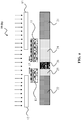
FIG. 1 orFIG. 2 , according to an embodiment of the invention. - FIG. 4
- shows an APD device according to an embodiment of the invention.
- FIG.5
- shows a step of a first alternative of a method according to an embodiment of the invention.
- FIG. 6
- shows a further step of the first alternative of a method according to an embodiment of the invention.
- FIG. 7
- shows a further step of the first alternative of a method according to an embodiment of the invention.
- FIG. 8
- shows a further step of the first alternative of a method according to an embodiment of the invention.
- FIG. 9
- shows a further step of the first alternative of a method according to an embodiment of the invention.
- FIG. 10
- shows a further step of the first alternative of a method according to an embodiment of the invention.
- FIG. 11
- shows a further step of the first alternative of a method according to an embodiment of the invention.
- FIG. 12
- shows a further step of the first alternative of a method according to an embodiment of the invention.
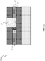
- FIG. 13
- shows a further step of the first alternative of a method according to an embodiment of the invention.
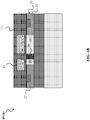
- FIG. 14
- shows a further step of the first alternative of a method according to an embodiment of the invention.
- FIG. 15
- shows a step of a second alternative of a method according to an embodiment of the invention.
- FIG. 16
- shows a further step of the second alternative of a method according to an embodiment of the invention.
- FIG. 17
- shows a further step of the second alternative of a method according to an embodiment of the invention.
- FIG. 18
- shows a further step of the second alternative of a method according to an embodiment of the invention.
- FIG. 19
- shows a further step of the second alternative of a method according to an embodiment of the invention.
- FIG. 20
- shows a further step of the second alternative of a method according to an embodiment of the invention.
- FIG. 21
- shows a further step of the second alternative of a method according to an embodiment of the invention.
-
FIG. 1 shows a first alternative (a) of ageneral method 10 according to an embodiment of the invention, andFIG. 2 shows a second alternative (a) of the general method according to an embodiment of the invention. Both alternatives have several steps in common, and both alternatives aremethods 10 for fabricating anAPD device 20 according to an embodiment of the invention, as it is for example shown inFIG. 3 orFIG. 4 . - In both alternatives (a) and (b), a
first contact region 21 and asecond contact region 22 are formed in asemiconductor layer 23. Thecontact regions semiconductor layer 23 may be the top layer of a silicon on insulator (SOI) substrate 50 (see, e.g.,FIG. 5 ). - Further, a
first mask layer 11 is formed in both alternatives (a) and (b) above at least afirst region 24 of thesemiconductor layer 23, wherein thefirst region 24 is adjacent to thefirst contact region 21. - Further, a
second mask layer 12 is formed above and laterally overlapping thefirst mask layer 11, wherein amask window 13 is defined by thefirst mask layer 11 and thesecond mask layer 12. Thefirst mask layer 11 and/or thesecond mask layer 12 are formed above asecond region 25 of thesemiconductor layer 23, wherein thesecond region 25 is adjacent to thesecond contact region 22. Thesecond region 25 may be configured to function as an amplification region in theAPD device 20. - In the first alternative (a) of
FIG. 1 , thefirst mask layer 11 may be formed only above thefirst region 24, i.e., only thesecond mask layer 12 may be formed above thesecond region 25. In the second alternative (b) ofFIG. 2 , thefirst mask layer 11 may be formed above thefirst region 24 and above thesecond region 25 of thesemiconductor layer 23, i.e., both mask layers 11 and 12 may be formed above thesecond region 25. - Further, in both alternatives (a) and (b), a
charge region 26 is formed in thesemiconductor layer 23 through themask window 13, wherein thecharge region 26 is formed between thefirst region 24 and thesecond region 25. Thecharge region 26 may be formed by implanting dopants through themask window 13 and into thesemiconductor layer 23. - In the first alternative (a) of
FIG. 1 , themethod 10 may comprise etching into thefirst mask layer 11 to obtain an opening in the first mask layer. Further, thesecond mask layer 12 may be formed such above thefirst mask layer 11, that themask window 13 is defined by the opening in thefirst mask layer 11. Thus, a width of themask window 13 may be controlled by controlling the width of the opening when etching into thefirst mask layer 11. - In the second alternative (b) of
FIG. 2 , thesecond mask layer 12 may be formed such above thesecond region 25, that themask window 13 is defined by a gap region where thefirst mask layer 11 and thesecond mask layer 12 do not laterally overlap. Thus, a width of themask window 13 may be controlled by controlling the lateral arrangement of thesecond mask layer 12 relative to thefirst mask layer 11 when forming thesecond mask layer 12, i.e., by controlling the overlap and non-overlap of the first and second mask layers 11, 12. - In both alternatives (a) and (b) an
absorption region 27 is the formed on thefirst region 24 using thefirst mask layer 11. This leads to theAPD device 20 shown inFIG. 3 . TheAPD device 20 shown inFIG. 2 may be a lateral SACM APD device, wherein theabsorption region 27, thecharge region 26, and the multiplication region (second region 25) are formed laterally between thefirst contact region 21 and thesecond contact region 22. The width wc of thecharge region 26 can be precisely controlled by themethod 10, in particular, down to 50nm or even less. Also a width wM of the multiplication region (i.e., of the second region 25) may be precisely controlled. -
FIG. 4 shows anotherAPD device 20, according to an embodiment of the invention, which builds on the embodiment shown inFIG. 3 . Same elements inFIG. 3 and inFIG. 4 are labelled with the same reference signs, and may be implemented likewise. - The
APD device 20 ofFIG. 4 includes further afirst contact 41 that is formed on thefirst contact region 21, and asecond contact 42 that is formed on thesecond contact region 22. In particular, thefirst contact 41 is formed on a highly-dopedregion 21a of thefirst contact region 21, and thesecond contact 42 is formed on a highly-dopedregion 22a of thesecond contact region 22. Preferably, thefirst contact region 21 is p-doped and the highly-dopedregion 21a is accordingly highly p-doped, and thesecond contact region 22 is n-doped and the highly-dopedregion 22a is highly n-doped. In this case also thecharge region 26 is p-doped. For instance, thecharge region 26 maybe p-doped to a lower extend as thefirst contact region 21. However, the connectivity types in theAPD device 20 can be reversed. - Notably, in the
APD device 20 shown inFIG. 4 , no contact is formed on theabsorption region 27, i.e., an upper surface (top surface) of theabsorption region 27 may be free/exposed. -
FIGs. 5-14 show steps of the first alternative (a) of aspecific method 10 according to an embodiment of the invention, which builds on the more general embodiment shown inFIG. 1 .FIGs. 5-7 andFIGs. 15-20 show steps of the second alternative (b) of aspecific method 10 according to an embodiment of the invention, which builds on the more general embodiment shown inFIG. 2 . That is,FIGs. 5-7 are valid for both alternatives (a) and (b). Same elements in all the figures are labelled with the same reference signs, and may be implemented likewise. -
FIG. 5 shows that in a first step of themethod 10, aSOI substrate 50 is provided, which includes asilicon substrate layer 51, an insulator layer 52 (silicon oxide layer) on thesubstrate layer 51, and a silicon layer as thesemiconductor layer 23. TheSOI substrate 50 may be provided in the form of a wafer. -
FIG. 6 shows that in a next step of themethod 10, thefirst contact region 21 and thesecond contact region 22 are formed in thesemiconductor layer 23. For instance, thefirst contact region 21 and thesecond contact region 22 are formed by implantation of respective dopants into the silicon, in order to form an n-doped and p-doped contact region, respectively. Before forming thefirst contact region 21 and thesecond contact region 22, athin oxide layer 60 maybe provided on thesemiconductor layer 23. For instance, thethin oxide layer 60 may have a thickness of 5-10nm. -
FIG. 7 shows that in a next step of themethod 10, amaterial 11a for thefirst mask layer 11 may be provided onto thethin oxide layer 60. In particular, a polycrystalline silicon layer may be deposited as the firstmask layer material 11a. -
FIG. 8 shows that in a next step of the first alternative (a) of themethod 10, the firstmask layer material 11a is patterned into thefirst mask layer 11. In this first alternative (a) of themethod 10, thefirst mask layer 11 is only formed above thefirst region 24 of thesemiconductor layer 23. Thefirst mask layer 11 may be patterned by lithography and etching. Thereby, theoxide layer 60 may function as an etch stop. -
FIG. 9 shows that in a next step of the first alternative (a) of themethod 10, thesecond mask layer 12 is formed above thefirst mask layer 11, wherein thesecond mask layer 12 laterally overlaps with thefirst mask layer 11. That may mean that thesecond mask layer 12 is arranged above at least a part of thefirst mask layer 11. Thesecond mask layer 12 is, in particular, formed such above thesecond region 25 that themask window 13 is defined by a gap region where thefirst mask layer 11 and thesecond mask layer 12 do not laterally overlap, i.e., thefirst mask layer 11 and thesecond mask layer 12 have an opening in a top view. The width of themask window 13 can be controlled by controlling the lateral arrangement of thesecond mask layer 12 relative to thefirst mask layer 11 when forming thesecond mask layer 12, i.e., by controlling the lateral overlap of thefirst mask layer 11 and thesecond mask layer 12. Further, thecharge region 26 is formed inFIG. 9 by implanting dopants through themask window 13, and into the semiconductor layer 23 (as indicated by the arrows). -
FIG. 10 shows that in a next step of the first alternative (a) of themethod 10, thesecond mask layer 12 maybe removed, and the highly-dopedregions first contact region 21 and thesecond contact region 22, respectively. These highly-dopedregions -
FIG. 11 shows that in a next step of the first alternative (a) of themethod 10, asacrificial layer 111 may be formed around thefirst mask layer 11. Thesacrificial layer 111 may comprise an oxide, for instance, silicon oxide. After forming thesacrificial layer 111, the top surface of the intermediate structure may be planarized, in order to form a planar upper surface. -
FIG. 12 shows that in a next step of the first alternative (a) of themethod 10, thefirst mask layer 11 may be removed above thefirst region 24, wherein asacrificial layer window 110 may be formed. That is, thewindow 110 may be formed by etching into thesacrificial layer 111, wherein thefirst mask layer 11 is removed. Thefirst mask layer 11 may be used to align the etching. Notably, the etching of thesacrificial layer window 110 may also etch into thefirst region 24 of thesemiconductor layer 23, thereby forming an indentation in thefirst region 24. -
FIG. 13 shows that in a next step of the first alternative (a) of themethod 10, absorption material may be deposited into thesacrificial layer window 110, onto thefirst region 24, thereby forming theabsorption region 27. Since thewindow 110 was etched using thefirst mask layer 11, the forming of theabsorption region 27 is also based on using thefirst mask layer 11. Further, theabsorption region 27 may be formed in the indentation of thesemiconductor layer 24, in particular, in an indentation spanning thefirst region 24. The step may also comprise CMP to planarize the surface of theabsorption region 27 and thesacrificial layer 111, respectively. In particular, theabsorption region 27 may comprise germanium as absorption material, or a germanium-based material. The absorption material may further be epitaxially grown into thewindow 110 to form theabsorption region 27. -
FIG. 14 shows that in a final step of the first alternative (a) of themethod 10, a back end of line (BEOL) processing may be performed, wherein thefirst contact 41 is formed on thefirst contact region 21 and thesecond contact 42 is formed on thesecond contact region 22a. This concludes the processing of theAPD device 20 according to the first alternative (a) of themethod 10. -
FIG. 15 shows a step of the second alternative (b) of themethod 10, which follows the step shown inFIG. 7 . InFIG. 15 , the firstmask layer material 11a is patterned into thefirst mask layer 11. In this first alternative (b) of themethod 10, thefirst mask layer 11 is formed both above thefirst region 24 and above thesecond region 25 of thesemiconductor layer 23. However, etching into thefirst mask layer 11 is performed to obtain anopening 140 in thefirst mask layer 13, namely located above the region of thesemiconductor layer 13 where thecharge region 26 will be formed (between thefirst region 24 and the second region 25). -
FIG. 16 shows that in a next step of the second alternative (b) of themethod 10, thesecond mask layer 12 is formed above thefirst mask layer 11, and laterally overlapping with thefirst mask layer 11. Thesecond mask layer 12 is, in particular, formed such above thesecond region 25, that themask window 13 is defined by theopening 140 in thefirst mask layer 11. The width of themask window 13 can be controlled by controlling the width of theopening 140 when etching into thefirst mask layer 11. Further, thecharge region 26 is formed inFIG. 16 , particularly by implanting dopants through themask window 13 into the semiconductor layer 23 (as indicated by the arrows). The doping may be as described above for the first alternative (a). -
FIG. 17 shows that in a next step of the second alternative (b) of themethod 10, thesecond mask layer 12 maybe removed, and the highly-dopedregions first contact region 21 and thesecond contact region 22, respectively. These highly-dopedregions -
FIG. 18 shows that in a next step of the second alternative (b) of themethod 10, asacrificial layer 111 may be formed around thefirst mask layer 11. Thesacrificial layer 111 may comprise an oxide, for instance, silicon oxide. After forming thesacrificial layer 111, the top surface of the structure may be planarized to form a planar surface. -
FIG. 19 shows that in the next step of the second alternative (b) of themethod 10, thefirst mask layer 11 may be removed above the first region 24 (here it may remain, however, above the second region 25), wherein asacrificial layer window 110 may be formed. That is, thewindow 110 may be formed by etching into thesacrificial layer 111, wherein thefirst mask layer 11 is removed. Thefirst mask layer 11 may thus be used, as in the first alternative (a), to align thewindow 110. Notably, the etching of thesacrificial layer window 110 may also etch into thefirst region 24 of thesemiconductor layer 23, to form an indentation. -
FIG. 20 shows that in a next step of the second alternative (b) of themethod 10, absorption material may be deposited into thesacrificial layer window 110, onto thefirst region 24, thereby forming theabsorption region 27. Further, theabsorption region 27 may be formed in the indentation of thefirst region 24 of thesemiconductor layer 24, in particular, in an indentation spanning thefirst region 24. The step may also comprise CMP to planarize the surface of theabsorption region 27 and thesacrificial layer 111. In particular, theabsorption region 27 may comprise germanium as absorption material, or a germanium-based material. The absorption material may be epitaxially grown into thewindow 110 to form theabsorption region 27. -
FIG. 21 shows that in a final step of the second alternative (b) of themethod 10, BEOL processing may be performed, wherein thefirst contact 41 is formed on thefirst contact region 21 and thesecond contact 42 is formed on the second contact region will 22. This concludes the processing of theAPD device 20 according to the second alternative (a) of themethod 10. - In the above-mentioned embodiments, certain materials may be used. In particular, the
semiconductor layer 23 may comprise silicon. Thefirst mask layer 11 may comprise poly-Si. Thesecond mask layer 12 may comprise a resist. Theabsorption region 27 may comprise germanium. The first andsecond contacts - The
method 10 according to its embodiments, implementations and alternatives described above for fabricating theAPD device 20, may in particular be used for avalanche photodetectors, photodetectors and single photon avalanche photodetectors. These devices are typically used in applications such as optical interconnections, optical communication, local optical quantum computing, quantum communication, terahertz communication, terahertz imaging, or sensing.
Claims (16)
- A method (10) for fabricating an avalanche photodiode device (20), the method (10) comprising:forming a first contact region (21) and a second contact region (22) in a semiconductor layer (23);forming a first mask layer (11) above at least a first region (24) of the semiconductor layer (23) adjacent to the first contact region (21);forming a second mask layer (12) above and laterally overlapping the first mask layer (11), wherein a mask window (13) is defined by the first mask layer (11) and the second mask layer (12), and wherein the first mask layer (11) and/or the second mask layer (12) are formed above a second region (25) of the semiconductor layer (23) adjacent to the second contact region (22);forming a charge region (26) in the semiconductor layer (23) through the mask window (13), wherein the charge region (26) is formed between the first region (24) and the second region (25); andforming an absorption region (27) on the first region (24) using the first mask layer (11).
- The method (10) according to claim 1, wherein:the charge region (26) is adjacent to the first region (24); and/orthe charge region (26) is laterally adjacent to the absorption region (27).
- The method (10) according to claim 1 or 2, wherein:
the charge region (26) has a width of below 100nm, in particular, has a width in a range of 50-60nm. - The method (10) according to one of the claims 1 to 3, wherein:
the second region (25) is configured to function as an amplification region in the avalanche photodiode device (20). - The method (10) according to one of the claims 1 to 4, wherein:
the charge region (26) is formed by implanting dopants through the mask window (13) into the semiconductor layer (23). - The method (10) according to one of the claims 1 to 5, wherein the first mask layer (11) is formed above the first region (24) and above the second region (25) of the semiconductor layer (23), and the method (10) further comprises:etching into the first mask layer (11) to obtain an opening (140) in the first mask layer (13); andforming the second mask layer (12) above the first mask layer (11) such that the mask window (13) is defined by the opening (140) in the first mask layer (11).
- The method (10) according to claim 6, wherein:
a width of the mask window (13) is controlled by controlling the width of the opening (140) when etching into the first mask layer (11). - The method (10) according to one of the claims 1 to 5, wherein the first mask layer (11) is formed only above the first region (24), and the method (10) further comprises:
forming the second mask layer (12) above the second region (25) such that the mask window (13) is defined by a gap region where the first mask layer (11) and the second mask layer (12) do not laterally overlap. - The method (10) according to claim 5, wherein:
a width of the mask window (13) is controlled by controlling the lateral arrangement of the second mask layer (12) relative to the first mask layer (11) when forming the second mask layer (12). - The method (10) according to one of the claims 1 to 9, wherein:
the first mask layer (11) is formed by depositing polycrystalline silicon onto the semiconductor layer (13) and then patterning the polycrystalline silicon. - The method (10) according to one of the claims 1 to 10, wherein:
the second mask layer (12) is formed by applying a resist and then patterning the resist. - The method (10) according to one of the claims 1 to 11, wherein the absorption region (27) is formed by:removing the second mask layer (12);forming a sacrificial layer (111) around the first mask layer (11);removing the first mask layer (11) above the first region (24), thereby forming a sacrificial layer window (110); anddepositing absorption material through the sacrificial layer window (110) onto the first region (24), thereby forming the absorption region (27).
- The method (10) according to one of the claims 1 to 12, wherein:the absorption region (27) is formed by absorption material that comprises germanium; and/orthe absorption region (27) is formed by epitaxial growth of the absorption material.
- The method (10) according to one of the claims 1 to 13, wherein the absorption region (27) is formed in an indentation of the semiconductor layer (24), in particular, in an indentation spanning the first region (24).
- The method (10) according to one of the claims 1 to 14, further comprising:forming a first contact (41) on the first contact region (21) and a second contact (42) on the second contact region (22); and/ornot forming any contact on the absorption region (27).
- An avalanche photodiode device (20) fabricated by using the method (10) according to one of the claims 1 to 15.
Priority Applications (3)
| Application Number | Priority Date | Filing Date | Title |
|---|---|---|---|
| EP20184864.5A EP3937262A1 (en) | 2020-07-09 | 2020-07-09 | A method for fabricating an avalanche photodiode device |
| US17/370,578 US11600735B2 (en) | 2020-07-09 | 2021-07-08 | Method for fabricating an avalanche photodiode device |
| CN202110772098.2A CN113921651A (en) | 2020-07-09 | 2021-07-08 | Method for manufacturing avalanche photodiode device |
Applications Claiming Priority (1)
| Application Number | Priority Date | Filing Date | Title |
|---|---|---|---|
| EP20184864.5A EP3937262A1 (en) | 2020-07-09 | 2020-07-09 | A method for fabricating an avalanche photodiode device |
Publications (1)
| Publication Number | Publication Date |
|---|---|
| EP3937262A1 true EP3937262A1 (en) | 2022-01-12 |
Family
ID=71574963
Family Applications (1)
| Application Number | Title | Priority Date | Filing Date |
|---|---|---|---|
| EP20184864.5A Pending EP3937262A1 (en) | 2020-07-09 | 2020-07-09 | A method for fabricating an avalanche photodiode device |
Country Status (3)
| Country | Link |
|---|---|
| US (1) | US11600735B2 (en) |
| EP (1) | EP3937262A1 (en) |
| CN (1) | CN113921651A (en) |
Citations (4)
| Publication number | Priority date | Publication date | Assignee | Title |
|---|---|---|---|---|
| US5385849A (en) * | 1993-05-17 | 1995-01-31 | Nec Corporation | Process of fabricating solid-state image pick-up device free from crystal defects in active region |
| US20070262475A1 (en) * | 2006-05-10 | 2007-11-15 | International Business Machines Corporation | Polysilicon hard mask for enhanced alignment signal |
| JP2015046429A (en) * | 2013-08-27 | 2015-03-12 | 株式会社日立製作所 | Light receiving element and manufacturing method thereof |
| US20190378949A1 (en) * | 2018-06-06 | 2019-12-12 | Fujitsu Limited | Optical semiconductor device and optical transceiver |
Family Cites Families (5)
| Publication number | Priority date | Publication date | Assignee | Title |
|---|---|---|---|---|
| US5238864A (en) * | 1990-12-21 | 1993-08-24 | Mitsubishi Denki Kabushiki Kaisha | Method of making solid-state imaging device |
| WO2014100506A1 (en) * | 2012-12-19 | 2014-06-26 | Intevac, Inc. | Grid for plasma ion implant |
| CN104347347A (en) * | 2013-08-05 | 2015-02-11 | 中芯国际集成电路制造(上海)有限公司 | Forming method of polysilicon resistor |
| US9755096B2 (en) * | 2014-03-10 | 2017-09-05 | Elenion Technologies, Llc | Lateral Ge/Si avalanche photodetector |
| KR102372892B1 (en) * | 2017-08-10 | 2022-03-10 | 삼성전자주식회사 | method of manufacturing integrated circuit device |
-
2020
- 2020-07-09 EP EP20184864.5A patent/EP3937262A1/en active Pending
-
2021
- 2021-07-08 US US17/370,578 patent/US11600735B2/en active Active
- 2021-07-08 CN CN202110772098.2A patent/CN113921651A/en active Pending
Patent Citations (4)
| Publication number | Priority date | Publication date | Assignee | Title |
|---|---|---|---|---|
| US5385849A (en) * | 1993-05-17 | 1995-01-31 | Nec Corporation | Process of fabricating solid-state image pick-up device free from crystal defects in active region |
| US20070262475A1 (en) * | 2006-05-10 | 2007-11-15 | International Business Machines Corporation | Polysilicon hard mask for enhanced alignment signal |
| JP2015046429A (en) * | 2013-08-27 | 2015-03-12 | 株式会社日立製作所 | Light receiving element and manufacturing method thereof |
| US20190378949A1 (en) * | 2018-06-06 | 2019-12-12 | Fujitsu Limited | Optical semiconductor device and optical transceiver |
Non-Patent Citations (1)
| Title |
|---|
| SRINIVASAN SRINIVASAN ASHWYN ET AL: "27 GHz Silicon-Contacted Waveguide-Coupled Ge/Si Avalanche Photodiode", JOURNAL OF LIGHTWAVE TECHNOLOGY, IEEE, USA, vol. 38, no. 11, 27 April 2020 (2020-04-27), pages 3044 - 3050, XP011790469, ISSN: 0733-8724, [retrieved on 20200527], DOI: 10.1109/JLT.2020.2986923 * |
Also Published As
| Publication number | Publication date |
|---|---|
| CN113921651A (en) | 2022-01-11 |
| US20220013682A1 (en) | 2022-01-13 |
| US11600735B2 (en) | 2023-03-07 |
Similar Documents
| Publication | Publication Date | Title |
|---|---|---|
| US9048371B2 (en) | Semiconductor devices including avalanche photodetector diodes integrated on waveguides and methods for fabricating the same | |
| JP5655153B2 (en) | Photodetector and photodetector circuit | |
| US9742147B2 (en) | Monolithic integrated photonics with lateral bipolar and BiCMOS | |
| KR101891150B1 (en) | Low voltage photodetectors | |
| US9329415B2 (en) | Method for forming an optical modulator | |
| US20250006856A1 (en) | Diode with light-sensitive intrinsic region | |
| US10580923B2 (en) | Optical semiconductor device and optical transceiver | |
| US20200313026A1 (en) | Method of fabrication of a photonic chip comprising an sacm-apd photodiode optically coupled to an integrated waveguide | |
| EP4207318B1 (en) | Avalanche photodetector and preparation method therefor | |
| US20150016769A1 (en) | Semiconductor devices including photodetectors integrated on waveguides and methods for fabricating the same | |
| US11600734B2 (en) | Avalanche photodiode device with a curved absorption region | |
| US11054674B2 (en) | PN-junction phase modulator in a large silicon waveguide platform | |
| EP3548963B1 (en) | Waveguide device and method of doping a waveguide device | |
| US11520113B1 (en) | Photodetectors and terminators including a tapered thickness | |
| US20190259900A1 (en) | Semiconductor light receiving element and manufacturing method | |
| US11600735B2 (en) | Method for fabricating an avalanche photodiode device | |
| US8022494B2 (en) | Photodetector and manufacturing method thereof | |
| US12176351B2 (en) | Photonics chips including a fully-depleted silicon-on-insulator field-effect transistor | |
| CN113451426A (en) | Photodetector with adjacent anode-cathode pairs | |
| KR101923730B1 (en) | A semiconductor laser and method of forming the same | |
| CN115377241A (en) | Single-chip photoelectric integrated planar avalanche photoelectric detection array chip on SOI and preparation method thereof | |
| CN113809198A (en) | Photodiode and/or PIN diode structure | |
| US10283665B2 (en) | Compensated photonic device structure and fabrication method thereof | |
| CN112599547A (en) | Semiconductor device and manufacturing method thereof | |
| US12550459B1 (en) | Integrated germanium photodiode with self-aligned implant and electrical contact |
Legal Events
| Date | Code | Title | Description |
|---|---|---|---|
| PUAI | Public reference made under article 153(3) epc to a published international application that has entered the european phase |
Free format text: ORIGINAL CODE: 0009012 |
|
| STAA | Information on the status of an ep patent application or granted ep patent |
Free format text: STATUS: THE APPLICATION HAS BEEN PUBLISHED |
|
| AK | Designated contracting states |
Kind code of ref document: A1 Designated state(s): AL AT BE BG CH CY CZ DE DK EE ES FI FR GB GR HR HU IE IS IT LI LT LU LV MC MK MT NL NO PL PT RO RS SE SI SK SM TR |
|
| B565 | Issuance of search results under rule 164(2) epc |
Effective date: 20201207 |
|
| STAA | Information on the status of an ep patent application or granted ep patent |
Free format text: STATUS: REQUEST FOR EXAMINATION WAS MADE |
|
| 17P | Request for examination filed |
Effective date: 20220712 |
|
| RBV | Designated contracting states (corrected) |
Designated state(s): AL AT BE BG CH CY CZ DE DK EE ES FI FR GB GR HR HU IE IS IT LI LT LU LV MC MK MT NL NO PL PT RO RS SE SI SK SM TR |