EP3937237A1 - Mixed poly pitch design solution for power trim - Google Patents
Mixed poly pitch design solution for power trim Download PDFInfo
- Publication number
- EP3937237A1 EP3937237A1 EP21184799.1A EP21184799A EP3937237A1 EP 3937237 A1 EP3937237 A1 EP 3937237A1 EP 21184799 A EP21184799 A EP 21184799A EP 3937237 A1 EP3937237 A1 EP 3937237A1
- Authority
- EP
- European Patent Office
- Prior art keywords
- pitch
- poly
- gate length
- cell
- cells
- Prior art date
- Legal status (The legal status is an assumption and is not a legal conclusion. Google has not performed a legal analysis and makes no representation as to the accuracy of the status listed.)
- Withdrawn
Links
Images














Classifications
-
- G—PHYSICS
- G06—COMPUTING OR CALCULATING; COUNTING
- G06F—ELECTRIC DIGITAL DATA PROCESSING
- G06F30/00—Computer-aided design [CAD]
- G06F30/30—Circuit design
- G06F30/39—Circuit design at the physical level
- G06F30/392—Floor-planning or layout, e.g. partitioning or placement
-
- H—ELECTRICITY
- H10—SEMICONDUCTOR DEVICES; ELECTRIC SOLID-STATE DEVICES NOT OTHERWISE PROVIDED FOR
- H10D—INORGANIC ELECTRIC SEMICONDUCTOR DEVICES
- H10D89/00—Aspects of integrated devices not covered by groups H10D84/00 - H10D88/00
- H10D89/10—Integrated device layouts
-
- G—PHYSICS
- G06—COMPUTING OR CALCULATING; COUNTING
- G06F—ELECTRIC DIGITAL DATA PROCESSING
- G06F30/00—Computer-aided design [CAD]
- G06F30/30—Circuit design
- G06F30/39—Circuit design at the physical level
- G06F30/398—Design verification or optimisation, e.g. using design rule check [DRC], layout versus schematics [LVS] or finite element methods [FEM]
-
- G—PHYSICS
- G06—COMPUTING OR CALCULATING; COUNTING
- G06F—ELECTRIC DIGITAL DATA PROCESSING
- G06F2111/00—Details relating to CAD techniques
- G06F2111/04—Constraint-based CAD
-
- G—PHYSICS
- G06—COMPUTING OR CALCULATING; COUNTING
- G06F—ELECTRIC DIGITAL DATA PROCESSING
- G06F2119/00—Details relating to the type or aim of the analysis or the optimisation
- G06F2119/06—Power analysis or power optimisation
-
- H—ELECTRICITY
- H10—SEMICONDUCTOR DEVICES; ELECTRIC SOLID-STATE DEVICES NOT OTHERWISE PROVIDED FOR
- H10D—INORGANIC ELECTRIC SEMICONDUCTOR DEVICES
- H10D84/00—Integrated devices formed in or on semiconductor substrates that comprise only semiconducting layers, e.g. on Si wafers or on GaAs-on-Si wafers
- H10D84/01—Manufacture or treatment
- H10D84/0123—Integrating together multiple components covered by H10D12/00 or H10D30/00, e.g. integrating multiple IGBTs
- H10D84/0126—Integrating together multiple components covered by H10D12/00 or H10D30/00, e.g. integrating multiple IGBTs the components including insulated gates, e.g. IGFETs
- H10D84/0135—Manufacturing their gate conductors
-
- H—ELECTRICITY
- H10—SEMICONDUCTOR DEVICES; ELECTRIC SOLID-STATE DEVICES NOT OTHERWISE PROVIDED FOR
- H10D—INORGANIC ELECTRIC SEMICONDUCTOR DEVICES
- H10D84/00—Integrated devices formed in or on semiconductor substrates that comprise only semiconducting layers, e.g. on Si wafers or on GaAs-on-Si wafers
- H10D84/01—Manufacture or treatment
- H10D84/0123—Integrating together multiple components covered by H10D12/00 or H10D30/00, e.g. integrating multiple IGBTs
- H10D84/0126—Integrating together multiple components covered by H10D12/00 or H10D30/00, e.g. integrating multiple IGBTs the components including insulated gates, e.g. IGFETs
- H10D84/0135—Manufacturing their gate conductors
- H10D84/0142—Manufacturing their gate conductors the gate conductors having different shapes or dimensions
-
- H—ELECTRICITY
- H10—SEMICONDUCTOR DEVICES; ELECTRIC SOLID-STATE DEVICES NOT OTHERWISE PROVIDED FOR
- H10D—INORGANIC ELECTRIC SEMICONDUCTOR DEVICES
- H10D84/00—Integrated devices formed in or on semiconductor substrates that comprise only semiconducting layers, e.g. on Si wafers or on GaAs-on-Si wafers
- H10D84/01—Manufacture or treatment
- H10D84/02—Manufacture or treatment characterised by using material-based technologies
- H10D84/03—Manufacture or treatment characterised by using material-based technologies using Group IV technology, e.g. silicon technology or silicon-carbide [SiC] technology
- H10D84/038—Manufacture or treatment characterised by using material-based technologies using Group IV technology, e.g. silicon technology or silicon-carbide [SiC] technology using silicon technology, e.g. SiGe
-
- H—ELECTRICITY
- H10—SEMICONDUCTOR DEVICES; ELECTRIC SOLID-STATE DEVICES NOT OTHERWISE PROVIDED FOR
- H10D—INORGANIC ELECTRIC SEMICONDUCTOR DEVICES
- H10D84/00—Integrated devices formed in or on semiconductor substrates that comprise only semiconducting layers, e.g. on Si wafers or on GaAs-on-Si wafers
- H10D84/80—Integrated devices formed in or on semiconductor substrates that comprise only semiconducting layers, e.g. on Si wafers or on GaAs-on-Si wafers characterised by the integration of at least one component covered by groups H10D12/00 or H10D30/00, e.g. integration of IGFETs
- H10D84/82—Integrated devices formed in or on semiconductor substrates that comprise only semiconducting layers, e.g. on Si wafers or on GaAs-on-Si wafers characterised by the integration of at least one component covered by groups H10D12/00 or H10D30/00, e.g. integration of IGFETs of only field-effect components
- H10D84/83—Integrated devices formed in or on semiconductor substrates that comprise only semiconducting layers, e.g. on Si wafers or on GaAs-on-Si wafers characterised by the integration of at least one component covered by groups H10D12/00 or H10D30/00, e.g. integration of IGFETs of only field-effect components of only insulated-gate FETs [IGFET]
- H10D84/83138—Integrated devices formed in or on semiconductor substrates that comprise only semiconducting layers, e.g. on Si wafers or on GaAs-on-Si wafers characterised by the integration of at least one component covered by groups H10D12/00 or H10D30/00, e.g. integration of IGFETs of only field-effect components of only insulated-gate FETs [IGFET] the IGFETs characterised by having different shapes or dimensions of their gate conductors
Definitions
- An integrated circuit is an electronic circuit manufactured into the surface of a thin substrate of semiconductor material.
- ICs are used in virtually all electronic equipment today and have revolutionized the world of electronics.
- Computers, mobile phones, and other digital home appliances are now inextricable parts of the structure of modern societies, made possible by the low cost of producing ICs.
- IC layout designs are optimized for speed and power before ICs are manufactured.
- first and second features are formed in direct contact
- additional features may be formed between the first and second features, such that the first and second features may not be in direct contact
- present disclosure may repeat reference numerals and/or letters in the various examples. This repetition is for the purpose of simplicity and clarity and does not in itself dictate a relationship between the various embodiments and/or configurations discussed.
- spatially relative terms such as “beneath,” “below,” “lower,” “above,” “upper” and the like, may be used herein for ease of description to describe one element or feature's relationship to another element(s) or feature(s) as illustrated in the figures.
- the spatially relative terms are intended to encompass different orientations of the device in use or operation in addition to the orientation depicted in the figures.
- the apparatus may be otherwise oriented (rotated 90 degrees or at other orientations) and the spatially relative descriptors used herein may likewise be interpreted accordingly.
- Trimming is typically conducted with laser. For example, one of the most common applications of trimming is conducted using laser to burn away a small portion of the circuit, such as resistors or transistors. Trimming of transistors causes changes in transistor performance, such as power consumption and operating speed. As will be discussed in details below, the trimming of even a few nanometers causes significant effects in power and speed of the IC. As a result, trimming needs to be carefully calculated for each individual cell and well-coordinated among different cells to achieve an overall optimization of the design and manufacturing of the entire circuit.
- FIG. 1 is a figure illustrating the effect of Lg+3nm G-bias in a mixed poly pitch upon power and speed according to an exemplary embodiment.
- the mixed poly pitch power trim design of the of systems and methods as disclosed herein implements the effect of Lg + GPM (for example, Lg+3nm) G-bias upon power and speed.
- Gate length (“Lg") expansion causes a bias called G-bias in speed-power figure as illustrated in Fig. 1 , where the horizontal axis is speed in GHz and the vertical is leakage power in nW.
- the three filled dots designate three different cells with threshold voltages, where SVT stands for standard threshold voltage, LVT stands for low threshold voltage and ⁇ LVT stands fo ultra-low threshold voltage.
- threshold voltage is related to leakage power and there are trade-offs between leakage power and speed. For example, for the fastest ⁇ LVT cell, the leakage power is also large. In comparison, LVT is relatively slower than ⁇ LVT but consumes less leakage power. SVT has even smaller leakage power than LVT but at the cost of even slower speed.
- G-bias is an effective approach to reduce device leakage for low power optimization.
- GPM 3nm, Lg + 3nm
- both leakage power and speed of the ⁇ LVT cell are reduced, which is designated by an empty dot connected to the original filled dot (Lg) with dashed line.
- the G-bias also reduces both leakage power and speed for both LVT and SVT cells, as illustrated in Fig. 1 .
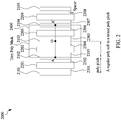
- FIG. 2 is a schematic illustrating a regular poly cell in a mixed poly pitch according to the exemplary embodiment.
- the Lg+3nm G-bias effect discussed in FIG. 1 above are further explained in FIG's. 2-5.
- FIG.'s 2 and 4 illustrate a regular poly pitch, while FIG. 4 is a cut-through cross-sectional view of FIG. 2 .
- FIG's. 3 and 5 illustrate an increased poly pitch Lg + GPM (for example, Lg+3nm), with FIG. 5 as the cut-through cross-sectional view of FIG. 3 .
- Lg + GPM for example, Lg+3nm
- Transistor gate pitch is also referred to as CPP (contacted poly pitch) and interconnect pitch is also referred to as MMP (minimum metal pitch).
- CPP contacted poly pitch
- MMP minimum metal pitch
- Integrated circuit layout design needs to be optimized, for power consumption or for speed, before they are used to manufacture integrated circuits.
- There are constraints on the floorplan of an IC layout design for example, cells cannot be freely moved or swapped because of their geometric constraints. Cells can only be moved with certain step sizes, and a cell or a minimum unit can only be moved to another location on the layout which can geometrically accommodate the cell or minimum unit.
- the poly cell 2000 includes poly lines 2101, 2102, 2103, 2104 and 2105 which are separated by a constant distance called poly pitch.
- Poly pitch is defined as the distance between the center of two closest poly lines, for example, 2101 and 2102.
- mid-diffusion (“MD") layers 2201, 2202, 2203 and 2204 are deployed.
- the MD layer is the diffusion layer manufactured in mid-end process, as compared to front-end process and back-end process. Front-end process refers to wafer processing operation, back-end process refers to assembly process, mid-end process refers to the operations in between.
- the MD layer refers to the diffusion layer between source/drain active area.
- Atomic diffusion in semiconductors refers to the migration of atoms, including host, dopant and impurities.
- Ga atoms can migrate over the Ga sublattice via jumps into nearest neighbor Ga vacancies, as can dopant atoms substituting on Ga sites.
- Spacers 2301-2308 are deployed between poly lines and diffusion layers to filled the space.
- a trim poly mask 2400 is deployed to cover at least partially the poly cell 2000. When the poly cell 2000 is cut along A-A', a cross-sectional view along A-A' is shown in Fig. 4 below.
- FIG. 3 is a schematic illustrating an increased poly pitch in a mixed poly pitch according to the exemplary embodiment.
- the increased poly pitch structure Lg + GPM (for example, Lg+3) of the of systems and methods as discussed in FIG. 1 above is illustrated in FIG. 3 .
- G-bias technique mentioned above requires poly pitch increase which comes with area scaling penalty.
- the spacers 3304 and 3305 on the left and right sides of the gate 3103 can be trimmed by, for example laser. Laser burns away certain amount of the spacer materials to increase the length of the gate 3103. The amount of the spacer trimmed away can be called gate parameter modification (GPM).
- GPM gate parameter modification
- GPM is 3nm .
- the length of the gate can be increased from Lg to Lg + GPM.
- the length of the gate can be increased from Lg to Lg + 3nm. Trimming can also be achieved by chemical etching and other physical and chemical methods. As discussed in Fig. 1 , when the gate length is increased from Lg to Lg + 3nm, G-bias effect decreases the speed of the device while at the same time decreases the leakage power of the device. On a design layout, some cells are functional cells on the speed critical unit while other functional cells are on non-timing critical unit.
- a decrease in speed as a result of increasing Lg to Lg + 3nm for functional cells on the speed critical unit would not be desirable, while a decrease in speed as a result of increasing Lg to Lg + 3nm for non-timing critical unit does not affect the overall performance of the design. Due to the G-bias effect discussed above, increasing Lg to Lg + 3nm for dummy cells also decreases leakage power of the cells on non-timing critical unit. Overall, when all cells on non-timing critical unit are trimmed to increase the gate length from Lg to Lg + 3nm, the overall speed of the circuit is not affected, while the overall leakage power of the circuit is reduced, according to G-bias effect.
- poly cell 3000 is a poly cell with extended gate length Lg + 3 nm, which means that the width of the gate poly line 3103 is increased by 3nm in the same poly pitch.
- neighboring spacers 3304 and 3305 are appropriately trimmed to accommodate the extension of poly line 3103.
- a cross-sectional view along line C-C' is shown in Fig. 5 below.
- FIG. 4 is a cross-sectional view along line A-A' in Fig. 2 of a normal pitch in a mixed poly pitch according to the exemplary embodiment. As discussed earlier, FIG. 4 illustrates a cut-through cross-sectional view of the regular poly pitch of systems and methods as disclosed in FIG. 2 above.
- the MD layers 4202 and 4203 correspond to diffusion layer 2202 and 2203 in Fig. 2 .
- the distance OA and OA' are equal to one poly pitch (1CPP, or simply CPP).
- the gate 4103 has a corresponding gate length Lg. 4501 and 4502 are source and drain respectively.
- FIG. 5 is a cross-sectional view along line C-C' in Fig. 3 of an extended poly pitch in a mixed poly pitch according to the exemplary embodiment.
- FIG. 5 illustrates a cut-through cross-sectional view of the increased poly pitch of systems and methods as disclosed in FIG. 3 .
- the gate 5103 is increased in length by 3nm, as a result, the poly pitch OC and OC' are also increased by 3nm (CPP+3), while the gate to MD spacing is kept unchanged.
- the gate length increase is achieved by trimming of neighboring spacer materials by the amount of GPM.
- the gate length increace invokes G-bias effect to reduce both speed and leakage power of the units. When such gate length increace is only applied to non-timing critical units, then the overall timing of the design is hardly affected, but the overall leakage power is reduced due to G-bias effect discussed earlier.
- FIG. 6 illustrates a mixed poly pitch design according to the exemplary embodiment.
- the mixed poly pitch in FIG. 6 can achieve larger process window, better PPA (performance power area) and more complex flow.
- the box with (CPP48, Lg) designate a poly cell with poly pitch 48 and regular gate length Lg;
- the middle box with (CPP48, Lg+3) designates a poly cell with poly pitch 48 and an enlarged (by 3nm) gate length Lg+3;
- the right box is another (CPP48, Lg) cell.
- the left cell is (CPP45, Lg) which designates poly pitch of 45 with a regular gate length Lg; the middle cell (CPP48, Lg) or (CPP48, Lg+3) is a poly pitch of 48 with a regular gate length Lg, or an extended gate length Lg+3; the right cell is another (CPP45, Lg).
- the three cells (CPP45, Lg)(CPP48, Lg)(CPP45, Lg) can be called a unit; alternatively.
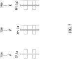
- FIG. 7 is a schematic illustrating three poly pitch and gate length combinations of equivalent cell types according to the exemplary embodiment.
- the poly cell 7100 PP_Lg is a cell with a poly pitch PP and regular gate length Lg; the poly cell 7200 PP1_Lg is a cell with a second poly pitch PP1 and regular gate length Lg; the poly cell 7300 PP1_Lg1 is a cell with the second poly pitch PP1 and an extended gate length Lg1.
- an equivalent cell type is a type of cells with the same number of pitches, which are no greater than the minimum unit to be fitted into the minimum unit.
- the poly cells 7200 and 7300 are of the same pitch size PP1 but with different gate length, Lg and Lg 1, respectively. By replacing the poly cell 7200 with 7300, leakage power is reduced due to G-bias as discussed above. On the other hand, when the poly cell 8300 is replaced by 7200, speed is increased due to G-bias discussed above.
- FIG. 8A and FIG. 8B are schematics illustrating asymmetric 2CPP and 3CPP designs of equivalent cell types according to the exemplary embodiment.
- FIG. 9A and FIG. 9B are schematics illustrating asymmetric 2CPP and 3CPP designs of equivalent cell types according to the exemplary embodiment.
- cells CPP45, CPP48
- Fig. 8A /B both CPP45 and CPP48 have the same number of poly pitches, for example, 2CPP, 3CPP or 4CPP; while in FIG.
- FIG. 9A /B CPP45 has 2CPP and CPP48 has 3CPP, or vice versa.
- FIG. 8A /B is called symmetric ratio
- FIG. 9A /B is called asymmetric ratio.
- cells can be replaced by equivalent cells to optimize speed and power.
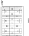
- FIG. 10 is a schematic illustrating cell abutment according to an exemplary embodiment.
- cell boundaries are aligned to MD centers, and cell boundary should be VDD or VSS. The implication will be discussed in FIG. 11 below.
- FIG. 11 is a schematic illustrating mixed poly pitch floorplan using minimal units of equivalent cell types according to the exemplary embodiment.
- symmetric ratio 2CPP minimum units are deployed on the floorplan, for example, minimum units 1101-1104 are four such 2CPP minimum units (CPP45, CPP48).
- Minimum units 1101 and 1103 are of the same configurations, with two CPP45 poly cells with regular gate length Lg on the left and two CPP48 poly cells with extended gate length Lg+3nm abutting to the right of (CPP45, Lg) cells.
- the right 2CPP of the minimum unit 1102 there are two CPP48 poly cells with regular gate length Lg.
- the right 2CPP of the minimum unit 1104 there is one CPP48 poly cell with regular gate length Lg, there is another CPP48 poly cell with extended gate length Lg+3nm.
- 1101_CPP45_1 and 1101_CPP45_2 are two poly lines with poly pitch 45, both with gate length Lg.
- 1101_CPP48_1 and 1101_CPP48_2 are two poly lines with poly pitch 48, but with gate length Lg+3nm.
- the minimum unit 1103 below 1101 has similar configurations.
- the minimum unit 1102 to the right of the minimum unit 1101 has a different configuration, in that, the poly lines 1102_CPP48_1 and 1102_CPP48_2 have a pitch size of 48 and regular gate length Lg.
- the minimum unit 1104 has two poly lines 1104_CPP48_1 and 1104_CPP48_2 with poly size 48, but the poly lines 1104_CPP48_1 and 1104_CPP48_2 have differing gate lengths: 1104_CPP48_1 has a gate length of Lg and 1104_CPP48_2 has a gate length of Lg+3nm.
- minimum units are rectangles of equal sizes deployed over the floorplan. Minimum units can contain different cells in the same equivalent cell types, i.e. with different leakage power and speed, without affecting the physical size of the minimum units. According to the abutment rules discussed on FIG. 14 , Type A can only abut Type C, and Type B can only abut Type D. As discussed above, by tweaking the equivalent cells in the same type, power and speed optimization can be achieved locally and globally with well-known algorithms.
- FIG. 12 is a schematic illustrating different combinations of mixed poly pitch and gate length of equivalent cell types according to the exemplary embodiment.
- minimum unit (2PP_Lg, 2PP1_Lg1) is illustrated, poly cell 2PP_Lg is on the left of the minimum unit and poly cell 2PP1_Lg1 is on the right.
- Different combinations of 2CPP, 3CPP, 4CPP and 5CPP are listed under FIG. 12A as equivalent types as discussed above.
- the equivalent type includes: 2PP_Lg, or 2PP1_Lg1, or PP_Lg+ P P1_Lg1; for 3CPP, the equivalent type includes: 2PP_Lg + PP1_Lg1, or PP_Lg + 2PP1_Lg1; for 4CPP, the equivalent type includes: 2PP_Lg + 2PP1_Lg1; and for 5CPP: 2PP_Lg + 2PP1_Lg1 + PP_Lg, or 2PP_Lg + 2PP1_Lg1 + PP1_Lg1.
- the equivalent type combination for 2CPP are: 2PP_Lg or 2PP1_Lg1 or PP_Lg + PP1_Lg; the equivalent type combination for 3CPP are: 2PP_Lg + PP1_Lg1, or PP Lg + 2PP1_Lg1, or PP_Lg + PP1_Lg1 + PP1_Lg; the equivalent type combination for 4CPP are: 2PP_Lg + 2PP1_Lg1, or 2PP_Lg + PP1_Lg1 + PP1_Lg.
- one cell can be replaced by another cell in the same equivalent type to achieve performance and/or power optimization without affecting the physical layout because cells of equivalent type can fit into the same minimum unit with varied power and speed.
- FIG. 13 is a schematic illustrating different combinations of mixed poly pitch and gate length of equivalent cell types according to the exemplary embodiment.
- a minimum unit (2PP_Lg, 3PP1_Lg1) is illustrated.
- Different combinations for 2CPP-6CPP equivalent types are listed.
- 2CPP equivalent type 2PP_Lg, or 2PP1_Lg1, or PP_Lg+PP_Lg1
- 3CPP equivalent type 2PP_Lg + PP1_Lg1, or 3PP1_Lg1, or 2PP1_Lg1 + PP_Lg
- 4CPP equivalent type 2PP_Lg + 2PP1_Lg1, or 3PP1_Lg1+PP_Lg
- 5CPP equivalent type 2PP_Lg + 3PP1_Lg1
- 6CPP equivalent type 2PP_Lg + 3PP1_Lg1 + PP_Lg, or 2PP_Lg + 4PP1_Lg1.
- equivalent type cells can be tweaked for performance and power optimization purposes.
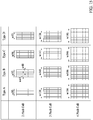
- FIG. 14 is a schematic illustrating the placement of four types of cells of equivalent cell types according to the exemplary embodiment.
- FIG. 15 is another schematic illustrating the placement of four types of cells of equivalent cell types according to the exemplary embodiment.
- Each type can be a 2CPP cell, a 3CPP cell or a 4CPP cell, etc.
- FIG. 14 is a schematic illustrating the placement of four types of cells of equivalent cell types according to the exemplary embodiment.
- FIG. 15 is another schematic illustrating the placement of four types of cells of equivalent cell types according to the exemplary embodiment.
- Each type can be a 2CPP cell, a 3CPP cell or a 4CPP cell, etc.
- 2CPP equivalent Type A 2CPP equivalent Type B, 2CPP equivalent Type C, 2CPP equivalent Type D, 3CPP equivalent Type A, 3CPP equivalent Type B, 3CPP equivalent Type C, 3CPP equivalent Type D, 4CPP equivalent Type A, 4CPP equivalent Type B, 4CPP equivalent Type C, 4CPP equivalent Type D.
- a minimum unit is (2CPP45, 2CPP48). As illustrated in FIGs. 14 and 15 , within the minimum unit, up to four CPP can be accommodated. As illustrated in FIG.
- the widths of equivalent Types A, B, C, D 2 pitch cells are: 90nm (45 pitch + 45 pitch), 93nm (45 pitch + 48 pitch), 96nm (48 pitch + 48 pitch), and 93nm (48 pitch + 45 pitch), respectively;
- the widths of Types A, B, C, D 3 pitch cells are 138nm (45 pitch + 45 pitch + 48 pitch), 141nm (45 pitch + 48 pitch + 48 pitch), 141nm (48 pitch + 48 pitch + 45 pitch), and 138nm (48 pitch + 45 pitch + 45 pitch), respectively; for 4 pitch cells, the widths for Types A-D are all the same: 186nm (45 pitch + 45 pitch + 48 pitch + 48 pitch).
- FIG. 16 is a flow chart illustrating a method of layout design optimization using mixed poly pitch cells for manufacturing integrated circuit according to the exemplary embodiment.
- the first step of the method 1610 is deploying an integrated circuit layout with mixed poly pitch cells.
- the integrated circuit layout includes a number of minimum unit each with at least a first number of first poly pitch cells with a first pitch size, and a second number of second poly pitch cells with a second pitch size. Both the first number and the second number are integers larger than 1.
- the first pitch size PP is different from the second pitch size PP1.
- a gate length of the first pitch size is Lg and a gate length of the second pitch size is Lg1.
- the method includes the next step 1620 of defining a plurality of equivalent cell types no greater than each of the number of minimum unit.
- the method includes the next step 1630 of optimizing the integrated circuit layout design by optimizing each of the minimum unit.
- the optimizing each of the minimum unit is achieved by step 1640 selecting one of the plurality of the equivalent cell types with a pitch size combination and a gate length combination which optimizes a speed and a total power of the integrated circuit.
- the optimization include placement optimization, clock tree timing optimization and routing optimization.
- the optimization processed can be repeated until the performance and/or power reaches predetermined values, which is step 1650.
- manufacturing the integrated circuit with the optimized integrated circuit layout deign.
- the minimum unit in this context is by definition the legalized step of moving on the layout floor plan, making the minimum units the smallest design blocks in the layout. During the optimization process, the optimization can be repeated until the power and/or speed reach predetermined values, or alternatively, the optimization can be repeated a predetermined number of iterations.
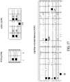
- FIG. 17 is a schematic illustrating the floorplans of three devices according to the exemplary embodiment.
- the layout of an inverter INVD occupies 2 pitches (2CPP).
- an AOI22 gate occupies 5 pitches (5CPP);
- a flip-flop with reset function occupies 13 pitches (13CPP).
- the minimum unit can choose a pitch size of 20 (20CPP).
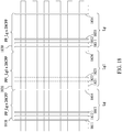
- FIG. 18 is a schematic illustrating mixed poly pitch floorplan of 20CPP according to the exemplary embodiment.
- a mixed poly pitch floorplan of 20 pitches can include PP_Lg ⁇ 20CPP, PP1_Lg1 ⁇ 20CPP, and PP_Lg ⁇ 20CPP.
- the minimum unit 1810 is a PP_Lg ⁇ 20CPP, which includes 20 regular gates, for example: 1811, 1812, 1813 and 1814;
- the minimum unit 1820 is a PP1_Lg1 ⁇ 20CPP, which includes 20 extended gates with gate length Lg1, for example: 1821, 1822, 1823 and 1824;
- the minimum unit 1830 is another PP_Lg ⁇ 20CPP, which includes 20 regular gates, for example: 1831, 1832, 1833, 1834.
- the 20CPP minimum units can be optimized for performance and for power, which will be discussed in FIGs 19 and 20 below.
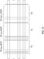
- FIG. 19 is a schematic illustrating mixed poly pitch floorplan for performance of 20CPP according to the exemplary embodiment.
- regular gate length is faster than extended gate length but has a larger leakage power. Accordingly, the ratio of 20CPP minimum unit in FIG. 18 above can be optimized for power or for performance.
- the floorplan in FIG. 19 is optimized for performance because there are more regular gates.
- FIG. 20 is a schematic illustrating mixed poly pitch floorplan for power saving of 20CPP according to the exemplary embodiment.
- FIG. 20 is optimized for power because there are more gates with extended gate length. As discussed above, the G-bias makes the leakage power smaller for gates with extended length.
- FIG. 21 is a schematic illustrating minimal cell movement in 20CPP floorplan according to the exemplary embodiment.
- the minimum cell movement within the minimum units is 3.
- a cell PP_Lg For example, for a cell PP_Lg, it can only move in steps of 3, after 15 steps, the cell PP_Lg moves the distance of one pitch 45; for a cell PP1_Lg1, it can also only move in steps of 3, after 16 steps, the cell PP1_Lg1 moves the distance of one pitch 48.
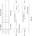
- FIG. 22 is a schematic illustrating cell swapping according to an exemplary embodiment.
- the cell 2201 A_Lg with shorter gate length Lg which is not on a critical path
- the cell 2204 B_Lg1 with longer gate length is located on a critical path and it needs to be optimized for speed, so the cell 2204 B_Lg1 is swapped to the cell 2203 B_Lg with shorter gate length Lg for optimized speed.
- the legalized step is a multiple of the minimum step 3, or 3 ⁇ steps, as discussed above.
- FIG. 23 is another schematic illustrating cell swapping according to the exemplary embodiment.
- cell B_Lg1 cannot be swapped to cell A_Lg because, for example, there is not enough space to accommodate cell B_Lg, or there is a mismatch in space configuration.
- cell B_Lg1 can be optimized without moving cell B_Lg1, instead, the gate length of cell B is modified to become B_Lg. According to G-bias discussed above, speed and/or power can be optimized through G-bias effect.
- FIG. 24 is a schematic illustrating a single cell height with mixed poly pitch floorplan and a hybrid cell height with mixed poly pitch floorplan according to the exemplary embodiment.
- FIG. 24A a regular single cell height mixed poly pitch floorplan is illustrated.
- FIG. 24B there are two difference cell heights: cell height 1 and cell height 2.
- FIG. 24B is hybrid cell height mixed poly pitch floor plan.
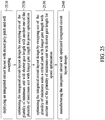
- FIG. 25 is a flow chart illustrating a method of layout design optimization using mixed poly pitch and cell swapping for manufacturing integrated circuit according to the exemplary embodiment.
- method of layout design optimization using mixed poly pitch and cell swapping for manufacturing integrated circuit includes the first step 2510 deploying an integrated circuit layout with mixed poly pitch and cell swapping, the integrated circuit layout includes a plurality of minimum units[2201-2204] each with at least a first number of first poly pitch cells with a first pitch size, and a second number of second poly pitch cells with a second pitch size, the first pitch size PP is different from the second pitch size PP1, the greatest common divisor of the first pitch size PP and the second pitch size PP1 is GCD, wherein GCD is an integer greater than 1; a gate length of the first pitch size is Lg; a gate length of the second pitch size is Lg1; Lg and Lg1 are capable of being extended to achieve G-bias for power and speed optimization of the minimum unit and the integrated circuit; and the size of the minimum unit is no smaller than
- the method includes the next step 2520 optimizing the integrated circuit layout design by swapping one of the plurality of minimum unit with shorter gate length with another one of the plurality of minimum unis with longer gate length for power optimization.
- the method includes the next step 2530 optimizing the integrated circuit layout design by swapping one of the plurality of minimum units on a critical path with longer gate length with another one of the plurality of minimum unis with shorter gate length for speed optimization.
- the last step 2540 of the method is manufacturing the integrated circuit with the optimized integrated circuit layout deign.
- FIG. 26 is a flow chart illustrating a method of layout design optimization using mixed poly pitch cells for manufacturing integrated circuit according to the exemplary embodiment.
- the next step is mixed poly pitch planning in floorplan by using the min.unit defined above. For example, normal Lg is for high performance, and Lg+3nm is implemented for leakage power reduction. Alternatively, cell layout for different types are planned. And the legalized step of site if equal to the min.unit.
- the placement step referring to FIG's 11-15, cells are placed according to the results of planning steps. After the placement step, clock tree synthesis, or CTS, is conducted. And signal routing step follows the CTS step.
- FIG. 27 is a flow chart illustrating a method of layout design with mixed poly pitch and cell swapping, according to the exemplary embodiment.
- the minim unit is the highest common factor. For example, find the max pitch of cells in the library as the min.unit. Refer to FIG. 17 and related discussions, for example, the min.unit is 20. Then use that min.unit (for example, 20) in the mixed poly planning. And the legalized step of site is the highest common factor of LG/Lg1, referring to FIG. 18-20 .
- poly alignment and PPA cell swap are conducted, referring to FIG's 21-24.
- clock tree synthesis, or CTS is conducted.
- signal routing step follows the CTS step.
- FIG. 28 is a system chart illustrating a layout design system according to the exemplary embodiment.
- a layout design system include at least a processor for processing all information related to design of floor plan and cell layout, etc.
- the layout design system also include at least a memory module for storing information related to design of floor plan and cell layout.
- the memory module can also be implemented to store software and tools for layout design and related tasks.
- the layout design system can include input and output modules, the layout design system can also be connected to network for information exchange.
- the layout design system can be connected to fabrication tools, after the layout design is finalized, the layout design is forwarded to the fabrication tool for fabrication of the integrated circuit according to the layout design.
- an integrated circuit with mixed poly pitch cells with a plurality of different pitch sizes includes: at least a minimum unit each with at least a first number of first poly pitch cells with a first pitch size, and a second number of second poly pitch cells with a second pitch size, the first pitch size PP is different from the second pitch size PP1, the greatest common divisor of the first pitch size PP and the second pitch size PP1 is GCD, wherein GCD is an integer greater than 1.
- the plurality of different pitch sizes is 2.
- a gate length of the first pitch size is Lg; a gate length of the second pitch size is Lg1, the minimum unit includes 2 poly cells with the first pitch size PP and the first gate length Lg, and 2 poly cells with the second pitch size PP1 and the second gate length Lg1.
- the minimum unit includes 2 poly cells with the first pitch size PP and the first gate length Lg, one poly cell with the second pitch size PP1 and the first gate length Lg, and one poly cell with the second pitch size PP1 and the second gate length Lg1.
- the minimum unit includes 2 poly cells with the first pitch size PP and the first gate length Lg, one poly cell with the first pitch size PP and the first gate length Lg, and one poly cell with the second pitch size PP1 and the second gate length Lg1.
- the minimum unit includes 2 poly cells with the first pitch size PP and the first gate length Lg, one poly cell with the first pitch size PP and the first gate length Lg, and one poly cell with the second pitch size PP1 and the first gate length Lg.
- the first pitch size PP is 45 and the second pitch size PP1 is 48
- the GCD is 3.
- the minimum unit includes 2 poly cells with the first pitch size PP and the first gate length Lg, and 3 poly cells with the second pitch size PP1 and the second gate length Lg1.
- the minimum unit includes 2 poly cells with the first pitch size PP and the first gate length Lg, and 2 poly cells with the second pitch size PP1 and the second gate length Lg1, and one poly cell with the first pitch size PP and the first gate length Lg.
- the minimum unit includes 2 poly cells with the first pitch size PP and the first gate length Lg, and 2 poly cells with the second pitch size PP1 and the first gate length Lg, and one poly cell with the second pitch size PP1 and the second gate length Lg1.
- a method of integrated circuit layout design optimization using mixed poly pitch cells for manufacturing integrated circuit includes: deploying an integrated circuit layout with mixed poly pitch cells, the integrated circuit layout includes: a number of minimum unit each with at least a first number of first poly pitch cells with a first pitch size, and a second number of second poly pitch cells with a second pitch size, wherein both the first number and the second number are integers larger than 1; the first pitch size PP is different from the second pitch size PP1, the greatest common divisor of the first pitch size PP and the second pitch size PP1 is GCD, wherein GCD is an integer greater than 1; a gate length of the first pitch size is Lg; a gate length of the second pitch size is Lg1; the method further includes defining a plurality of equivalent cell types no greater than each of the number of minimum unit; optimizing the integrated circuit layout design by optimizing each of the minimum unit, optimizing each of the minimum unit further includes: selecting one of the plurality of the equivalent cell types with a pitch size
- the method further includes: optimizing the integrated circuit layout design by optimizing each of the minimum unit one more time until the speed and the total power reach predetermined values.
- the method further includes: optimizing the integrated circuit layout design by optimizing each of the minimum unit a predetermined number of iterations.
- an integrated circuit layout with mixed poly pitch cells with a plurality of different pitch sizes includes: a plurality of minimum units each with at least a first number of first poly pitch cells with a first pitch size, and a second number of second poly pitch cells with a second pitch size, the first pitch size PP is different from the second pitch size PP1, a gate length of the first pitch size is Lg; a gate length of the second pitch size is Lg1; the layout is formed based on a modification of an initial layout, wherein the modification comprises increasing a length of one of Lg and Lg1 by a gate parameter modification magnitude selected to achieve G-bias of the minimum unit.
- the size of the minimum unit is no smaller than the largest cell pitch size in a standard library. According to an exemplary embodiment, the size of the minimum unit is no smaller than the size of a flip-flop with reset function in the standard library. According to an exemplary embodiment, the size of the minimum unit is greater than 13. According to an exemplary embodiment, the size of the minimum unit is 20. According to an exemplary embodiment, one of the plurality of minimum units with shorter gate length is swapped with another one of the plurality of minimum unis with longer gate length for power optimization. According to an exemplary embodiment, one of the plurality of minimum units on a critical path with longer gate length is swapped with another one of the plurality of minimum unis with shorter gate length for speed optimization.
Landscapes
- Engineering & Computer Science (AREA)
- Computer Hardware Design (AREA)
- Physics & Mathematics (AREA)
- Theoretical Computer Science (AREA)
- Evolutionary Computation (AREA)
- Geometry (AREA)
- General Engineering & Computer Science (AREA)
- General Physics & Mathematics (AREA)
- Architecture (AREA)
- Design And Manufacture Of Integrated Circuits (AREA)
Abstract
An integrated circuit with mixed poly pitch cells with a plurality of different pitch sizes is disclosed. The integrated circuit includes: at least a minimum unit each with at least a first number of first poly pitch cells with a first pitch size (CPP45), and a second number of second poly pitch cells with a second pitch size (CPP48), the first pitch size PP is different from the second pitch size PP1, the greatest common divisor of the first pitch size PP and the second pitch size PP1 is GCD, wherein GCD is an integer greater than 1; a gate length of the first pitch size is Lg; a gate length of the second pitch size is Lg1; Lg and Lg1 are capable of being extended to achieve G-bias for power and speed optimization of the minimum unit and the integrated circuit.
Description
- An integrated circuit (IC) is an electronic circuit manufactured into the surface of a thin substrate of semiconductor material. ICs are used in virtually all electronic equipment today and have revolutionized the world of electronics. Computers, mobile phones, and other digital home appliances are now inextricable parts of the structure of modern societies, made possible by the low cost of producing ICs. IC layout designs are optimized for speed and power before ICs are manufactured.
- Aspects of the present disclosure are best understood from the following detailed description when read with the accompanying figures. It is noted that, in accordance with the standard practice in the industry, various features are not drawn to scale. In fact, the dimensions of the various features may be arbitrarily increased or reduced for clarity of discussion.
-
FIG. 1 is a figure illustrating the effect of Lg+3nm G-bias in a mixed poly pitch upon power and speed according to an exemplary embodiment. -
FIG. 2 is a schematic illustrating a regular poly cell in a mixed poly pitch according to the exemplary embodiment. -
FIG. 3 is a schematic illustrating an increased poly pitch in a mixed poly pitch according to the exemplary embodiment. -
FIG. 4 is a cross-sectional view along line A-A' inFig. 2 of a normal pitch in a mixed poly pitch according to the exemplary embodiment. -
FIG. 5 is a cross-sectional view along line C-C' inFig. 3 of an extended poly pitch in a mixed poly pitch according to the exemplary embodiment. -
FIG. 6 illustrates a mixed poly pitch design according to the exemplary embodiment. -
FIG. 7 is a schematic illustrating three poly pitch and gate length combinations of equivalent cell types according to the exemplary embodiment. -
FIG. 8A and FIG. 8B are schematics illustrating symmetric 2CPP and 3CPP designs of equivalent cell types according to the exemplary embodiment. -
FIG. 9A and FIG. 9B are schematics illustrating asymmetric 2CPP and 3CPP designs of equivalent cell types according to the exemplary embodiment. -
FIG. 10 is a schematic illustrating cell abutment according to an exemplary embodiment. -
FIG. 11 is a schematic illustrating mixed poly pitch floorplan of equivalent cell types according to the exemplary embodiment. -
FIG. 12 is a schematic illustrating different combinations of mixed poly pitch and gate length of equivalent cell types according to the exemplary embodiment. -
FIG. 13 is a schematic illustrating different combinations of mixed poly pitch and gate length of equivalent cell types according to the exemplary embodiment. -
FIG. 14 is a schematic illustrating the placement of four types of cells of equivalent cell types according to the exemplary embodiment. -
FIG. 15 is another schematic illustrating the placement of four types of cells of equivalent cell types according to the exemplary embodiment. -
FIG. 16 is a flow chart illustrating a method of layout design optimization using mixed poly pitch cells for manufacturing integrated circuit according to the exemplary embodiment. -
FIG. 17 is a schematic illustrating the floorplans of three devices according to the exemplary embodiment. -
FIG. 18 is a schematic illustrating mixed poly pitch floorplan of 20CPP according to the exemplary embodiment. -
FIG. 19 is a schematic illustrating mixed poly pitch floorplan for performance of 20CPP according to the exemplary embodiment. -
FIG. 20 is a schematic illustrating mixed poly pitch floorplan for power saving of 20CPP according to the exemplary embodiment. -
FIG. 21 is a schematic illustrating minimal cell movement in 20CPP floorplan according to the exemplary embodiment. -
FIG. 22 is a schematic illustrating cell swapping according to an exemplary embodiment. -
FIG. 23 is another schematic illustrating cell swapping according to the exemplary embodiment. -
FIG. 24 is a schematic illustrating a single cell height with mixed poly pitch floorplan and a hybrid cell height with mixed poly pitch floorplan according to the exemplary embodiment. -
FIG. 25 is a flow chart illustrating a method of layout design with mixed poly pitch and cell swapping according to the exemplary embodiment. -
FIG. 26 is a flow chart illustrating a method of layout design optimization using mixed poly pitch cells for manufacturing integrated circuit according to the exemplary embodiment. -
FIG. 27 is a flow chart illustrating a method of layout design with mixed poly pitch and cell swapping according to the exemplary embodiment. -
FIG. 28 is a system chart illustrating a layout design system according to the exemplary embodiment. - The following disclosure provides many different embodiments, or examples, for implementing different features of the provided subject matter. Specific examples of components and arrangements are described below to simplify the present disclosure. These are, of course, merely examples and are not intended to be limiting. For example, the formation of a first feature over or on a second feature in the description that follows may include embodiments in which the first and second features are formed in direct contact, and may also include embodiments in which additional features may be formed between the first and second features, such that the first and second features may not be in direct contact. In addition, the present disclosure may repeat reference numerals and/or letters in the various examples. This repetition is for the purpose of simplicity and clarity and does not in itself dictate a relationship between the various embodiments and/or configurations discussed.
- Further, spatially relative terms, such as "beneath," "below," "lower," "above," "upper" and the like, may be used herein for ease of description to describe one element or feature's relationship to another element(s) or feature(s) as illustrated in the figures. The spatially relative terms are intended to encompass different orientations of the device in use or operation in addition to the orientation depicted in the figures. The apparatus may be otherwise oriented (rotated 90 degrees or at other orientations) and the spatially relative descriptors used herein may likewise be interpreted accordingly.
- During the manufacturing of integrated circuits, certain operating parameters of the circuits need to be adjusted, or "trimmed". Trimming is typically conducted with laser. For example, one of the most common applications of trimming is conducted using laser to burn away a small portion of the circuit, such as resistors or transistors. Trimming of transistors causes changes in transistor performance, such as power consumption and operating speed. As will be discussed in details below, the trimming of even a few nanometers causes significant effects in power and speed of the IC. As a result, trimming needs to be carefully calculated for each individual cell and well-coordinated among different cells to achieve an overall optimization of the design and manufacturing of the entire circuit. The following paragraphs will give detailed discussions regarding the performance optimization for individual cells, for a group of neighboring cells, and for cells of greater distance away within the same circuit design. Within the entire circuit design, few cells can be trimmed without affecting the performance of the entire circuit, and in return, trimming effects caused by some cells can sometimes be compensated by the trimming of other cells. Often times, speed gain is at the cost of power, and vice versa. Trimming can be implemented to increase the gate length of certain devices, the change in gate length can be measured by a gate parameter modification (GPM). Trimming effects, and the combination of trimming effects will be discussed in further details from
Fig. 1 to Fig. 25 . -
FIG. 1 is a figure illustrating the effect of Lg+3nm G-bias in a mixed poly pitch upon power and speed according to an exemplary embodiment. The mixed poly pitch power trim design of the of systems and methods as disclosed herein implements the effect of Lg + GPM (for example, Lg+3nm) G-bias upon power and speed. Gate length ("Lg") expansion causes a bias called G-bias in speed-power figure as illustrated inFig. 1 , where the horizontal axis is speed in GHz and the vertical is leakage power in nW. According to some embodiments, the three filled dots, namely SVT, LVT and µLVT, designate three different cells with threshold voltages, where SVT stands for standard threshold voltage, LVT stands for low threshold voltage and µLVT stands fo ultra-low threshold voltage. As illustrated inFig. 1 , threshold voltage is related to leakage power and there are trade-offs between leakage power and speed. For example, for the fastest µLVT cell, the leakage power is also large. In comparison, LVT is relatively slower than µLVT but consumes less leakage power. SVT has even smaller leakage power than LVT but at the cost of even slower speed. - In the same figure, three empty dots with corresponding dashed lines illustrate the bias effect when the gate length is increased (gate length extension). Gate length extension can effectively reduce leakage power because of smaller subthreshold leakage. According to some embodiments, the bias illustrated in
Fig. 1 is called G-bias. G-bias is an effective approach to reduce device leakage for low power optimization. According to some embodiments, when G-bias is applied to the µLVT cell by increasing the gate length by GPM (for example, GPM = 3nm, Lg + 3nm), both leakage power and speed of the µLVT cell are reduced, which is designated by an empty dot connected to the original filled dot (Lg) with dashed line. Similarly, the G-bias also reduces both leakage power and speed for both LVT and SVT cells, as illustrated inFig. 1 . -
FIG. 2 is a schematic illustrating a regular poly cell in a mixed poly pitch according to the exemplary embodiment. The Lg+3nm G-bias effect discussed inFIG. 1 above are further explained in FIG's. 2-5. FIG.'s 2 and 4 illustrate a regular poly pitch, whileFIG. 4 is a cut-through cross-sectional view ofFIG. 2 . In comparison, FIG's. 3 and 5 illustrate an increased poly pitch Lg + GPM (for example, Lg+3nm), withFIG. 5 as the cut-through cross-sectional view ofFIG. 3 . In the advanced technology, it is a challenge to etch-back metal gates during manufacturing semiconductor devices due to no selectivity between silicide and metal gates. Transistor gate pitch is also referred to as CPP (contacted poly pitch) and interconnect pitch is also referred to as MMP (minimum metal pitch). Some manufacturers have reported their 10 nm process as having a 64 nm transistor gate pitch and 48 nm interconnect pitch. - Integrated circuit layout design needs to be optimized, for power consumption or for speed, before they are used to manufacture integrated circuits. There are constraints on the floorplan of an IC layout design, for example, cells cannot be freely moved or swapped because of their geometric constraints. Cells can only be moved with certain step sizes, and a cell or a minimum unit can only be moved to another location on the layout which can geometrically accommodate the cell or minimum unit. When cells need to be moved or swapped for power and speed optimizations, such constraints in poly pitch, step sizes and minimum unit size, etc.
- According to some embodiments, the
poly cell 2000 includespoly lines trim poly mask 2400 is deployed to cover at least partially thepoly cell 2000. When thepoly cell 2000 is cut along A-A', a cross-sectional view along A-A' is shown inFig. 4 below. -
FIG. 3 is a schematic illustrating an increased poly pitch in a mixed poly pitch according to the exemplary embodiment. The increased poly pitch structure Lg + GPM (for example, Lg+3) of the of systems and methods as discussed inFIG. 1 above is illustrated inFIG. 3 . With the development of technology, while poly pitch keeps scaling aggressively, it remains very challenging to extend gate length in the same poly pitch. G-bias technique mentioned above requires poly pitch increase which comes with area scaling penalty. According to some embodiments, thespacers gate 3103 can be trimmed by, for example laser. Laser burns away certain amount of the spacer materials to increase the length of thegate 3103. The amount of the spacer trimmed away can be called gate parameter modification (GPM). According to some embodiments, GPM is 3nm . For example, the length of the gate can be increased from Lg to Lg + GPM. According to some embodiments, the length of the gate can be increased from Lg to Lg + 3nm. Trimming can also be achieved by chemical etching and other physical and chemical methods. As discussed inFig. 1 , when the gate length is increased from Lg to Lg + 3nm, G-bias effect decreases the speed of the device while at the same time decreases the leakage power of the device. On a design layout, some cells are functional cells on the speed critical unit while other functional cells are on non-timing critical unit. A decrease in speed as a result of increasing Lg to Lg + 3nm for functional cells on the speed critical unit would not be desirable, while a decrease in speed as a result of increasing Lg to Lg + 3nm for non-timing critical unit does not affect the overall performance of the design. Due to the G-bias effect discussed above, increasing Lg to Lg + 3nm for dummy cells also decreases leakage power of the cells on non-timing critical unit. Overall, when all cells on non-timing critical unit are trimmed to increase the gate length from Lg to Lg + 3nm, the overall speed of the circuit is not affected, while the overall leakage power of the circuit is reduced, according to G-bias effect. Those skilled in the art should appreciate that the GPM can be numbers other than 3nm, and 3nm is only an example for illustration purpose. According to some embodiments,poly cell 3000 is a poly cell with extended gate length Lg + 3 nm, which means that the width of thegate poly line 3103 is increased by 3nm in the same poly pitch. And neighboringspacers poly line 3103. A cross-sectional view along line C-C' is shown inFig. 5 below. -
FIG. 4 is a cross-sectional view along line A-A' inFig. 2 of a normal pitch in a mixed poly pitch according to the exemplary embodiment. As discussed earlier,FIG. 4 illustrates a cut-through cross-sectional view of the regular poly pitch of systems and methods as disclosed inFIG. 2 above. According to some embodiments, the MD layers 4202 and 4203 correspond todiffusion layer Fig. 2 . The distance OA and OA' are equal to one poly pitch (1CPP, or simply CPP). Thegate 4103 has a corresponding gate length Lg. 4501 and 4502 are source and drain respectively. -
FIG. 5 is a cross-sectional view along line C-C' inFig. 3 of an extended poly pitch in a mixed poly pitch according to the exemplary embodiment. As discussed earlier,FIG. 5 illustrates a cut-through cross-sectional view of the increased poly pitch of systems and methods as disclosed inFIG. 3 . As a comparison toFig. 4 , thegate 5103 is increased in length by 3nm, as a result, the poly pitch OC and OC' are also increased by 3nm (CPP+3), while the gate to MD spacing is kept unchanged. As discussed earlier, the gate length increase is achieved by trimming of neighboring spacer materials by the amount of GPM. The gate length increace invokes G-bias effect to reduce both speed and leakage power of the units. When such gate length increace is only applied to non-timing critical units, then the overall timing of the design is hardly affected, but the overall leakage power is reduced due to G-bias effect discussed earlier. -
FIG. 6 illustrates a mixed poly pitch design according to the exemplary embodiment. According to some embodiments, the mixed poly pitch inFIG. 6 can achieve larger process window, better PPA (performance power area) and more complex flow. In the "as is" column, the box with (CPP48, Lg) designate a poly cell with poly pitch 48 and regular gate length Lg; the middle box with (CPP48, Lg+3) designates a poly cell with poly pitch 48 and an enlarged (by 3nm) gate length Lg+3; the right box is another (CPP48, Lg) cell. In comparison, in the "Mixed Poly Pitch" column, the left cell is (CPP45, Lg) which designates poly pitch of 45 with a regular gate length Lg; the middle cell (CPP48, Lg) or (CPP48, Lg+3) is a poly pitch of 48 with a regular gate length Lg, or an extended gate length Lg+3; the right cell is another (CPP45, Lg). The three cells (CPP45, Lg)(CPP48, Lg)(CPP45, Lg) can be called a unit; alternatively. -
FIG. 7 is a schematic illustrating three poly pitch and gate length combinations of equivalent cell types according to the exemplary embodiment. According to some embodiments, thepoly cell 7100 PP_Lg is a cell with a poly pitch PP and regular gate length Lg; thepoly cell 7200 PP1_Lg is a cell with a second poly pitch PP1 and regular gate length Lg; thepoly cell 7300 PP1_Lg1 is a cell with the second poly pitch PP1 and an extended gate length Lg1. According to some embodiments, for example, PP = 45, PP1 = 48, and Lg1 = Lg + 3. According to some embodiments, an equivalent cell type is a type of cells with the same number of pitches, which are no greater than the minimum unit to be fitted into the minimum unit. Within the same equivalent cell type, there can be different combinations of pitch sizes and gate lengths. Because they have the same number of pitches, one cell in the same equivalent type can sometimes replace another cell with a different gate length. Due to the G-bias discussed above, such replacement can change the speed and power of the integrated circuit. Accordingly, speed and power optimization can be achieved by tweaking different cells within the same equivalent cell type. For example, thepoly cells Lg 1, respectively. By replacing thepoly cell 7200 with 7300, leakage power is reduced due to G-bias as discussed above. On the other hand, when the poly cell 8300 is replaced by 7200, speed is increased due to G-bias discussed above. Because the number of equivalent cells in each type is rather limited especially when the size of the minimum unit is small. In the worst case scenario, a minimum or maximum value can be located when all equivalent cells are exhausted in the same type. This tweaking process is also called optimization. Various optimization algorithms are well known. -
FIG. 8A and FIG. 8B are schematics illustrating asymmetric 2CPP and 3CPP designs of equivalent cell types according to the exemplary embodiment.FIG. 9A and FIG. 9B are schematics illustrating asymmetric 2CPP and 3CPP designs of equivalent cell types according to the exemplary embodiment. In bothFIG. 8A /B andFIG. 9A /B, cells (CPP45, CPP48) are called minimum units which are capable of being repeated over the floorplan as basic blocks. The difference is that inFig. 8A /B, both CPP45 and CPP48 have the same number of poly pitches, for example, 2CPP, 3CPP or 4CPP; while inFIG. 9A /B, CPP45 has 2CPP and CPP48 has 3CPP, or vice versa.FIG. 8A /B is called symmetric ratio,FIG. 9A /B is called asymmetric ratio. As discussed above, in each 2CPP or 3CPP equivalent types, cells can be replaced by equivalent cells to optimize speed and power. -
FIG. 10 is a schematic illustrating cell abutment according to an exemplary embodiment. According to some embodiments, in general standard cell structure, cell boundaries are aligned to MD centers, and cell boundary should be VDD or VSS. The implication will be discussed inFIG. 11 below. -
FIG. 11 is a schematic illustrating mixed poly pitch floorplan using minimal units of equivalent cell types according to the exemplary embodiment. According to some embodiments, symmetric ratio 2CPP minimum units are deployed on the floorplan, for example, minimum units 1101-1104 are four such 2CPP minimum units (CPP45, CPP48). Minimum units 1101 and 1103 are of the same configurations, with two CPP45 poly cells with regular gate length Lg on the left and two CPP48 poly cells with extended gate length Lg+3nm abutting to the right of (CPP45, Lg) cells. On the left 2CPP of the minimum unit 1102, there are two CPP45 poly cells with regular gate length Lg. On the right 2CPP of the minimum unit 1102, there are two CPP48 poly cells with regular gate length Lg. In comparison, the right 2CPP of the minimum unit 1104, there is one CPP48 poly cell with regular gate length Lg, there is another CPP48 poly cell with extended gate length Lg+3nm. More specifically, in the minimum unit 1101, 1101_CPP45_1 and 1101_CPP45_2 are two poly lines withpoly pitch 45, both with gate length Lg. In comparison, 1101_CPP48_1 and 1101_CPP48_2 are two poly lines with poly pitch 48, but with gate length Lg+3nm. The minimum unit 1103 below 1101 has similar configurations. By contrast, the minimum unit 1102 to the right of the minimum unit 1101 has a different configuration, in that, the poly lines 1102_CPP48_1 and 1102_CPP48_2 have a pitch size of 48 and regular gate length Lg. In comparison to the minimum unit 1102, the minimum unit 1104 has two poly lines 1104_CPP48_1 and 1104_CPP48_2 with poly size 48, but the poly lines 1104_CPP48_1 and 1104_CPP48_2 have differing gate lengths: 1104_CPP48_1 has a gate length of Lg and 1104_CPP48_2 has a gate length of Lg+3nm. As discussed above, regular gate length Lg is for high performance, and Lg+3nm is for leakage power reduction. As discussed above, the minimum units are rectangles of equal sizes deployed over the floorplan. Minimum units can contain different cells in the same equivalent cell types, i.e. with different leakage power and speed, without affecting the physical size of the minimum units. According to the abutment rules discussed onFIG. 14 , Type A can only abut Type C, and Type B can only abut Type D. As discussed above, by tweaking the equivalent cells in the same type, power and speed optimization can be achieved locally and globally with well-known algorithms. -
FIG. 12 is a schematic illustrating different combinations of mixed poly pitch and gate length of equivalent cell types according to the exemplary embodiment. InFIG. 12A , minimum unit (2PP_Lg, 2PP1_Lg1) is illustrated, poly cell 2PP_Lg is on the left of the minimum unit and poly cell 2PP1_Lg1 is on the right. Different combinations of 2CPP, 3CPP, 4CPP and 5CPP are listed underFIG. 12A as equivalent types as discussed above. For 2CPP, the equivalent type includes: 2PP_Lg, or 2PP1_Lg1, or PP_Lg+ P P1_Lg1; for 3CPP, the equivalent type includes: 2PP_Lg + PP1_Lg1, or PP_Lg + 2PP1_Lg1; for 4CPP, the equivalent type includes: 2PP_Lg + 2PP1_Lg1; and for 5CPP: 2PP_Lg + 2PP1_Lg1 + PP_Lg, or 2PP_Lg + 2PP1_Lg1 + PP1_Lg1.FIG. 12B is a variation ofFIG. 12A because 2PP1_Lg1 = PP1_Lg + PP1_Lg1. Similarly, the equivalent type combination for 2CPP are: 2PP_Lg or 2PP1_Lg1 or PP_Lg + PP1_Lg; the equivalent type combination for 3CPP are: 2PP_Lg + PP1_Lg1, or PP Lg + 2PP1_Lg1, or PP_Lg + PP1_Lg1 + PP1_Lg; the equivalent type combination for 4CPP are: 2PP_Lg + 2PP1_Lg1, or 2PP_Lg + PP1_Lg1 + PP1_Lg. As discussed above, one cell can be replaced by another cell in the same equivalent type to achieve performance and/or power optimization without affecting the physical layout because cells of equivalent type can fit into the same minimum unit with varied power and speed. -
FIG. 13 is a schematic illustrating different combinations of mixed poly pitch and gate length of equivalent cell types according to the exemplary embodiment. InFIG. 13A , a minimum unit (2PP_Lg, 3PP1_Lg1) is illustrated. Different combinations for 2CPP-6CPP equivalent types are listed. For 2CPP equivalent type: 2PP_Lg, or 2PP1_Lg1, or PP_Lg+PP_Lg1; for 3CPP equivalent type: 2PP_Lg + PP1_Lg1, or 3PP1_Lg1, or 2PP1_Lg1 + PP_Lg; for 4CPP equivalent type: 2PP_Lg + 2PP1_Lg1, or 3PP1_Lg1+PP_Lg; for 5CPP equivalent type: 2PP_Lg + 3PP1_Lg1; for 6CPP equivalent type: 2PP_Lg + 3PP1_Lg1 + PP_Lg, or 2PP_Lg + 4PP1_Lg1.FIG. 13B illustrates three equivalent type embodiments for 3PP1_Lg1, where 3PP1_Lg1 = 2PP1_Lg + PP1_Lg1, or PP1_Lg1 + 2PP1_Lg. As discussed above, equivalent type cells can be tweaked for performance and power optimization purposes. -
FIG. 14 is a schematic illustrating the placement of four types of cells of equivalent cell types according to the exemplary embodiment.FIG. 15 is another schematic illustrating the placement of four types of cells of equivalent cell types according to the exemplary embodiment. According to some embodiments, there are four types of poly cells: Type A, Type B, Type C and Type D. Each type can be a 2CPP cell, a 3CPP cell or a 4CPP cell, etc. InFIG. 14 , three are 12 cells illustrated: 2CPP equivalent Type A , 2CPP equivalent Type B, 2CPP equivalent Type C, 2CPP equivalent Type D, 3CPP equivalent Type A, 3CPP equivalent Type B, 3CPP equivalent Type C, 3CPP equivalent Type D, 4CPP equivalent Type A, 4CPP equivalent Type B, 4CPP equivalent Type C, 4CPP equivalent Type D. A minimum unit is (2CPP45, 2CPP48). As illustrated inFIGs. 14 and15 , within the minimum unit, up to four CPP can be accommodated. As illustrated inFIG. 15 , the widths of equivalent Types A, B, C,D 2 pitch cells are: 90nm (45 pitch + 45 pitch), 93nm (45 pitch + 48 pitch), 96nm (48 pitch + 48 pitch), and 93nm (48 pitch + 45 pitch), respectively; the widths of Types A, B, C,D 3 pitch cells are 138nm (45 pitch + 45 pitch + 48 pitch), 141nm (45 pitch + 48 pitch + 48 pitch), 141nm (48 pitch + 48 pitch + 45 pitch), and 138nm (48 pitch + 45 pitch + 45 pitch), respectively; for 4 pitch cells, the widths for Types A-D are all the same: 186nm (45 pitch + 45 pitch + 48 pitch + 48 pitch). -
FIG. 16 is a flow chart illustrating a method of layout design optimization using mixed poly pitch cells for manufacturing integrated circuit according to the exemplary embodiment. The first step of themethod 1610 is deploying an integrated circuit layout with mixed poly pitch cells. The integrated circuit layout includes a number of minimum unit each with at least a first number of first poly pitch cells with a first pitch size, and a second number of second poly pitch cells with a second pitch size. Both the first number and the second number are integers larger than 1. The first pitch size PP is different from the second pitch size PP1. A gate length of the first pitch size is Lg and a gate length of the second pitch size is Lg1. The method includes thenext step 1620 of defining a plurality of equivalent cell types no greater than each of the number of minimum unit. The equivalent cell types are discussed above inFIGs. 7-15 . The method includes thenext step 1630 of optimizing the integrated circuit layout design by optimizing each of the minimum unit. The optimizing each of the minimum unit is achieved bystep 1640 selecting one of the plurality of the equivalent cell types with a pitch size combination and a gate length combination which optimizes a speed and a total power of the integrated circuit. The optimization include placement optimization, clock tree timing optimization and routing optimization. The optimization processed can be repeated until the performance and/or power reaches predetermined values, which isstep 1650. Atstep 1660, manufacturing the integrated circuit with the optimized integrated circuit layout deign. The minimum unit in this context is by definition the legalized step of moving on the layout floor plan, making the minimum units the smallest design blocks in the layout. During the optimization process, the optimization can be repeated until the power and/or speed reach predetermined values, or alternatively, the optimization can be repeated a predetermined number of iterations. -
FIG. 17 is a schematic illustrating the floorplans of three devices according to the exemplary embodiment. On the left, the layout of an inverter INVD occupies 2 pitches (2CPP). In the middle, an AOI22 gate occupies 5 pitches (5CPP); on the right, a flip-flop with reset function occupies 13 pitches (13CPP). For a minimum unit to accommodate all cells in a library, for example a standard library, the minimum unit can choose a pitch size of 20 (20CPP). -
FIG. 18 is a schematic illustrating mixed poly pitch floorplan of 20CPP according to the exemplary embodiment. According to some embodiments, a mixed poly pitch floorplan of 20 pitches can include PP_Lg × 20CPP, PP1_Lg1 × 20CPP, and PP_Lg × 20CPP. According to some embodiments, theminimum unit 1810 is a PP_Lg × 20CPP, which includes 20 regular gates, for example: 1811, 1812, 1813 and 1814; theminimum unit 1820 is a PP1_Lg1 × 20CPP, which includes 20 extended gates with gate length Lg1, for example: 1821, 1822, 1823 and 1824; theminimum unit 1830 is another PP_Lg × 20CPP, which includes 20 regular gates, for example: 1831, 1832, 1833, 1834. The 20CPP minimum units can be optimized for performance and for power, which will be discussed inFIGs 19 and20 below. -
FIG. 19 is a schematic illustrating mixed poly pitch floorplan for performance of 20CPP according to the exemplary embodiment. As discussed above, regular gate length is faster than extended gate length but has a larger leakage power. Accordingly, the ratio of 20CPP minimum unit inFIG. 18 above can be optimized for power or for performance. The floorplan inFIG. 19 is optimized for performance because there are more regular gates. - In comparison,
FIG. 20 is a schematic illustrating mixed poly pitch floorplan for power saving of 20CPP according to the exemplary embodiment. Instead of optimized for performance,FIG. 20 is optimized for power because there are more gates with extended gate length. As discussed above, the G-bias makes the leakage power smaller for gates with extended length. -
FIG. 21 is a schematic illustrating minimal cell movement in 20CPP floorplan according to the exemplary embodiment. According to some embodiments, the minimum cell movement within the minimum unit is the greatest common divisor (GCD) of the two different pitches, PP and PP1. This is also called the legalized step of the site. For example, when PP = 45, and PP1 = 48, then the GCD of PP and PP1 is 3. Accordingly, the minimum cell movement is 3 and the legalized movement of the site is 3. For minimum units of both PP_Lg × 20CPP and PP1_Lg1 × 20CPP, the minimum cell movement within the minimum units is 3. For example, for a cell PP_Lg, it can only move in steps of 3, after 15 steps, the cell PP_Lg moves the distance of onepitch 45; for a cell PP1_Lg1, it can also only move in steps of 3, after 16 steps, the cell PP1_Lg1 moves the distance of one pitch 48. -
FIG. 22 is a schematic illustrating cell swapping according to an exemplary embodiment. According to some embodiments, when thecell 2201 A_Lg with shorter gate length Lg, which is not on a critical path, can be swapped to thecell 2202 A_Lg1 with longer gate length Lg1 for optimized lowered power. In comparison, thecell 2204 B_Lg1 with longer gate length is located on a critical path and it needs to be optimized for speed, so thecell 2204 B_Lg1 is swapped to thecell 2203 B_Lg with shorter gate length Lg for optimized speed. During the cell swapping either for power or for speed, the legalized step is a multiple of theminimum step -
FIG. 23 is another schematic illustrating cell swapping according to the exemplary embodiment. In comparison toFIG. 22 , cell B_Lg1 cannot be swapped to cell A_Lg because, for example, there is not enough space to accommodate cell B_Lg, or there is a mismatch in space configuration. Under this condition, according to some embodiments, cell B_Lg1 can be optimized without moving cell B_Lg1, instead, the gate length of cell B is modified to become B_Lg. According to G-bias discussed above, speed and/or power can be optimized through G-bias effect. -
FIG. 24 is a schematic illustrating a single cell height with mixed poly pitch floorplan and a hybrid cell height with mixed poly pitch floorplan according to the exemplary embodiment. InFIG. 24A , a regular single cell height mixed poly pitch floorplan is illustrated. In comparison, inFIG. 24B , there are two difference cell heights:cell height 1 andcell height 2.FIG. 24B is hybrid cell height mixed poly pitch floor plan. -
FIG. 25 is a flow chart illustrating a method of layout design optimization using mixed poly pitch and cell swapping for manufacturing integrated circuit according to the exemplary embodiment. According to some embodiments, method of layout design optimization using mixed poly pitch and cell swapping for manufacturing integrated circuit includes thefirst step 2510 deploying an integrated circuit layout with mixed poly pitch and cell swapping, the integrated circuit layout includes a plurality of minimum units[2201-2204] each with at least a first number of first poly pitch cells with a first pitch size, and a second number of second poly pitch cells with a second pitch size, the first pitch size PP is different from the second pitch size PP1, the greatest common divisor of the first pitch size PP and the second pitch size PP1 is GCD, wherein GCD is an integer greater than 1; a gate length of the first pitch size is Lg; a gate length of the second pitch size is Lg1; Lg and Lg1 are capable of being extended to achieve G-bias for power and speed optimization of the minimum unit and the integrated circuit; and the size of the minimum unit is no smaller than the largest cell pitch size in a standard library. The method includes thenext step 2520 optimizing the integrated circuit layout design by swapping one of the plurality of minimum unit with shorter gate length with another one of the plurality of minimum unis with longer gate length for power optimization. The method includes thenext step 2530 optimizing the integrated circuit layout design by swapping one of the plurality of minimum units on a critical path with longer gate length with another one of the plurality of minimum unis with shorter gate length for speed optimization. Thelast step 2540 of the method is manufacturing the integrated circuit with the optimized integrated circuit layout deign. -
FIG. 26 is a flow chart illustrating a method of layout design optimization using mixed poly pitch cells for manufacturing integrated circuit according to the exemplary embodiment. According to some embodiments, referring to FIG's 7 -10, define the minimum unit as the CPP combination, for example: min.unit = combination (PP_Lg, PP1_Lg1∥PP1_Lg1'). After the cell mixed poly pitch planning, the next step is mixed poly pitch planning in floorplan by using the min.unit defined above. For example, normal Lg is for high performance, and Lg+3nm is implemented for leakage power reduction. Alternatively, cell layout for different types are planned. And the legalized step of site if equal to the min.unit. In the placement step, referring to FIG's 11-15, cells are placed according to the results of planning steps. After the placement step, clock tree synthesis, or CTS, is conducted. And signal routing step follows the CTS step. -
FIG. 27 is a flow chart illustrating a method of layout design with mixed poly pitch and cell swapping, according to the exemplary embodiment. According to some embodiments, referring to FIG's 17-24, the minim unit is the highest common factor. For example, find the max pitch of cells in the library as the min.unit. Refer toFIG. 17 and related discussions, for example, the min.unit is 20. Then use that min.unit (for example, 20) in the mixed poly planning. And the legalized step of site is the highest common factor of LG/Lg1, referring toFIG. 18-20 . Before the placement step, poly alignment and PPA cell swap are conducted, referring to FIG's 21-24. Then, similar toFIG. 26 , after the placement step, clock tree synthesis, or CTS, is conducted. And signal routing step follows the CTS step. -
FIG. 28 is a system chart illustrating a layout design system according to the exemplary embodiment. According to some embodiments, a layout design system include at least a processor for processing all information related to design of floor plan and cell layout, etc. The layout design system also include at least a memory module for storing information related to design of floor plan and cell layout. The memory module can also be implemented to store software and tools for layout design and related tasks. According to some embodiments, the layout design system can include input and output modules, the layout design system can also be connected to network for information exchange. According to some embodiments, the layout design system can be connected to fabrication tools, after the layout design is finalized, the layout design is forwarded to the fabrication tool for fabrication of the integrated circuit according to the layout design. - According to an exemplary embodiment, an integrated circuit with mixed poly pitch cells with a plurality of different pitch sizes is disclosed. The integrated circuit includes: at least a minimum unit each with at least a first number of first poly pitch cells with a first pitch size, and a second number of second poly pitch cells with a second pitch size, the first pitch size PP is different from the second pitch size PP1, the greatest common divisor of the first pitch size PP and the second pitch size PP1 is GCD, wherein GCD is an integer greater than 1.
- According to an exemplary embodiment, the plurality of different pitch sizes is 2. According to an exemplary embodiment, a gate length of the first pitch size is Lg; a gate length of the second pitch size is Lg1, the minimum unit includes 2 poly cells with the first pitch size PP and the first gate length Lg, and 2 poly cells with the second pitch size PP1 and the second gate length Lg1. According to an exemplary embodiment, the minimum unit includes 2 poly cells with the first pitch size PP and the first gate length Lg, one poly cell with the second pitch size PP1 and the first gate length Lg, and one poly cell with the second pitch size PP1 and the second gate length Lg1. According to an exemplary embodiment, the minimum unit includes 2 poly cells with the first pitch size PP and the first gate length Lg, one poly cell with the first pitch size PP and the first gate length Lg, and one poly cell with the second pitch size PP1 and the second gate length Lg1. According to an exemplary embodiment, the minimum unit includes 2 poly cells with the first pitch size PP and the first gate length Lg, one poly cell with the first pitch size PP and the first gate length Lg, and one poly cell with the second pitch size PP1 and the first gate length Lg. According to an exemplary embodiment, the first pitch size PP is 45 and the second pitch size PP1 is 48, the GCD is 3. According to an exemplary embodiment, the minimum unit includes 2 poly cells with the first pitch size PP and the first gate length Lg, and 3 poly cells with the second pitch size PP1 and the second gate length Lg1. According to an exemplary embodiment, the minimum unit includes 2 poly cells with the first pitch size PP and the first gate length Lg, and 2 poly cells with the second pitch size PP1 and the second gate length Lg1, and one poly cell with the first pitch size PP and the first gate length Lg. According to an exemplary embodiment, the minimum unit includes 2 poly cells with the first pitch size PP and the first gate length Lg, and 2 poly cells with the second pitch size PP1 and the first gate length Lg, and one poly cell with the second pitch size PP1 and the second gate length Lg1.
- According to an exemplary embodiment, a method of integrated circuit layout design optimization using mixed poly pitch cells for manufacturing integrated circuit is disclosed. The method includes: deploying an integrated circuit layout with mixed poly pitch cells, the integrated circuit layout includes: a number of minimum unit each with at least a first number of first poly pitch cells with a first pitch size, and a second number of second poly pitch cells with a second pitch size, wherein both the first number and the second number are integers larger than 1; the first pitch size PP is different from the second pitch size PP1, the greatest common divisor of the first pitch size PP and the second pitch size PP1 is GCD, wherein GCD is an integer greater than 1; a gate length of the first pitch size is Lg; a gate length of the second pitch size is Lg1; the method further includes defining a plurality of equivalent cell types no greater than each of the number of minimum unit; optimizing the integrated circuit layout design by optimizing each of the minimum unit, optimizing each of the minimum unit further includes: selecting one of the plurality of the equivalent cell types with a pitch size combination and a gate length combination which optimizes a speed and a total power of the integrated circuit. the last step of the method is manufacturing the integrated circuit with the optimized integrated circuit layout deign.
- According to an exemplary embodiment, the method further includes: optimizing the integrated circuit layout design by optimizing each of the minimum unit one more time until the speed and the total power reach predetermined values. According to an exemplary embodiment, the method further includes: optimizing the integrated circuit layout design by optimizing each of the minimum unit a predetermined number of iterations.
- According to an exemplary embodiment, an integrated circuit layout with mixed poly pitch cells with a plurality of different pitch sizes is disclosed. The integrated circuit layout includes: a plurality of minimum units each with at least a first number of first poly pitch cells with a first pitch size, and a second number of second poly pitch cells with a second pitch size, the first pitch size PP is different from the second pitch size PP1, a gate length of the first pitch size is Lg; a gate length of the second pitch size is Lg1; the layout is formed based on a modification of an initial layout, wherein the modification comprises increasing a length of one of Lg and Lg1 by a gate parameter modification magnitude selected to achieve G-bias of the minimum unit. According to an exemplary embodiment, the size of the minimum unit is no smaller than the largest cell pitch size in a standard library. According to an exemplary embodiment, the size of the minimum unit is no smaller than the size of a flip-flop with reset function in the standard library. According to an exemplary embodiment, the size of the minimum unit is greater than 13. According to an exemplary embodiment, the size of the minimum unit is 20. According to an exemplary embodiment, one of the plurality of minimum units with shorter gate length is swapped with another one of the plurality of minimum unis with longer gate length for power optimization. According to an exemplary embodiment, one of the plurality of minimum units on a critical path with longer gate length is swapped with another one of the plurality of minimum unis with shorter gate length for speed optimization.
- The foregoing outlines features of several embodiments so that those skilled in the art may better understand the aspects of the present disclosure. Those skilled in the art should appreciate that they may readily use the present disclosure as a basis for designing or modifying other processes and structures for carrying out the same purposes and/or achieving the same advantages of the embodiments introduced herein. Those skilled in the art should also realize that such equivalent constructions do not depart from the spirit and scope of the present disclosure, and that they may make various changes, substitutions, and alterations herein without departing from the spirit and scope of the present disclosure.
Claims (10)
- An integrated circuit with mixed poly pitch cells with a plurality of different pitch sizes, the integrated circuit comprising:at least a minimum unit each with at least a first number of first poly pitch cells with a first pitch size, and a second number of second poly pitch cells with a second pitch size,wherein the first pitch size PP is different from the second pitch size PP1, andwherein the greatest common divisor of the first pitch size PP and the second pitch size PP1 is GCD, wherein GCD is an integer greater than 1.
- The circuit of claim 1, wherein the plurality of different pitch sizes is 2.
- The circuit of claim 2, wherein a gate length of the first pitch size is Lg, wherein a gate length of the second pitch size is Lg1, wherein the minimum unit includes 2 poly cells with the first pitch size PP and the first gate length Lg, and 2 poly cells with the second pitch size PP1 and the second gate length Lg1.
- The circuit of claim 3, wherein the minimum unit includes 2 poly cells with the first pitch size PP and the first gate length Lg, one poly cell with the second pitch size PP1 and the first gate length Lg, and one poly cell with the second pitch size PP1 and the second gate length Lg1.
- The circuit of claim 3, wherein the minimum unit includes 2 poly cells with the first pitch size PP and the first gate length Lg, one poly cell with the first pitch size PP and the first gate length Lg, and one poly cell with the second pitch size PP1 and the second gate length Lg1.
- The circuit of claim 3, wherein the minimum unit includes 2 poly cells with the first pitch size PP and the first gate length Lg, one poly cell with the first pitch size PP and the first gate length Lg, and one poly cell with the second pitch size PP1 and the first gate length Lg.
- The circuit of claim 3, wherein the first pitch size PP is 45 and the second pitch size PP1 is 48, the GCD is 3.
- The circuit of claim 3, wherein the minimum unit includes 2 poly cells with the first pitch size PP and the first gate length Lg, and 3 poly cells with the second pitch size PP1 and the second gate length Lg1.
- The circuit of claim 3, wherein the minimum unit includes 2 poly cells with the first pitch size PP and the first gate length Lg, and 2 poly cells with the second pitch size PP1 and the second gate length Lg1, and one poly cell with the first pitch size PP and the first gate length Lg.
- The circuit of claim 3, wherein the minimum unit includes 2 poly cells with the first pitch size PP and the first gate length Lg, and 2 poly cells with the second pitch size PP1 and the first gate length Lg, and one poly cell with the second pitch size PP1 and the second gate length Lg1.
Applications Claiming Priority (1)
| Application Number | Priority Date | Filing Date | Title |
|---|---|---|---|
| US16/925,483 US11755808B2 (en) | 2020-07-10 | 2020-07-10 | Mixed poly pitch design solution for power trim |
Publications (1)
| Publication Number | Publication Date |
|---|---|
| EP3937237A1 true EP3937237A1 (en) | 2022-01-12 |
Family
ID=77042696
Family Applications (1)
| Application Number | Title | Priority Date | Filing Date |
|---|---|---|---|
| EP21184799.1A Withdrawn EP3937237A1 (en) | 2020-07-10 | 2021-07-09 | Mixed poly pitch design solution for power trim |
Country Status (5)
| Country | Link |
|---|---|
| US (4) | US11755808B2 (en) |
| EP (1) | EP3937237A1 (en) |
| JP (1) | JP2022016402A (en) |
| CN (1) | CN113392614A (en) |
| TW (1) | TW202203073A (en) |
Families Citing this family (3)
| Publication number | Priority date | Publication date | Assignee | Title |
|---|---|---|---|---|
| DE102017127276A1 (en) * | 2017-08-30 | 2019-02-28 | Taiwan Semiconductor Manufacturing Co., Ltd. | STANDARD CELLS AND ADAPTATIONS FROM THEREOF WITHIN A STANDARD CELL LIBRARY |
| CN110416296B (en) * | 2018-04-26 | 2021-03-26 | 苏州能讯高能半导体有限公司 | Semiconductor device, semiconductor chip and semiconductor device manufacturing method |
| US11755808B2 (en) * | 2020-07-10 | 2023-09-12 | Taiwan Semiconductor Manufacturing Company Limited | Mixed poly pitch design solution for power trim |
Citations (5)
| Publication number | Priority date | Publication date | Assignee | Title |
|---|---|---|---|---|
| US20100169847A1 (en) * | 2005-05-06 | 2010-07-01 | Tela Innovations. Inc., A Delaware Corporation | Standard cells having transistors annotated for gate-length biasing |
| US20140115554A1 (en) * | 2012-10-23 | 2014-04-24 | Arm Limited | Method of generating a layout of an integrated circuit comprising both standard cells and at least one memory instance |
| US20160111421A1 (en) * | 2014-10-21 | 2016-04-21 | Mark S. Rodder | Multiple cpp for increased source/drain area for fets including in a critical speed path |
| US20160269004A1 (en) * | 2015-03-10 | 2016-09-15 | International Business Machines Corporation | High-speed latch circuits by selective use of large gate pitch |
| EP3079172A1 (en) * | 2015-04-08 | 2016-10-12 | MediaTek Inc. | Cell layout utilizing boundary cell with mixed poly pitch within integrated circuit |
Family Cites Families (45)
| Publication number | Priority date | Publication date | Assignee | Title |
|---|---|---|---|---|
| JPS55115353A (en) * | 1979-02-27 | 1980-09-05 | Fujitsu Ltd | Cell rotatable by 90 |
| JP3600393B2 (en) * | 1997-02-10 | 2004-12-15 | 株式会社東芝 | Semiconductor device and manufacturing method thereof |
| US6393601B1 (en) * | 1997-04-14 | 2002-05-21 | Matsushita Electric Industrial Co., Ltd. | Layout designing apparatus for integrated circuit, transistor size determining apparatus, circuit characteristic evaluating method, and transistor size determining method |
| JP2002124585A (en) * | 2000-10-17 | 2002-04-26 | Hitachi Ltd | Nonvolatile semiconductor memory device and method of manufacturing the same |
| WO2002033544A1 (en) * | 2000-10-17 | 2002-04-25 | Pdf Solutions, Incorporated | Method for optimizing the characteristics of integrated circuits components from circuit speficications |
| AU2002230574A1 (en) * | 2000-10-30 | 2002-05-15 | Advanced Micro Devices Inc. | Doping for flash memory cell |
| JP3829088B2 (en) * | 2001-03-29 | 2006-10-04 | 株式会社東芝 | Semiconductor memory device |
| JP4190791B2 (en) * | 2002-04-12 | 2008-12-03 | エルピーダメモリ株式会社 | Manufacturing method of semiconductor integrated circuit device |
| JP2004086546A (en) * | 2002-08-27 | 2004-03-18 | Matsushita Electric Ind Co Ltd | Circuit simulation method |
| US6734521B2 (en) * | 2002-08-30 | 2004-05-11 | Texas Instruments Incorporated | Integrated circuit cells |
| JP4533645B2 (en) * | 2004-03-02 | 2010-09-01 | 株式会社東芝 | Standard cell layout design method and computer-readable recording medium storing layout design software |
| US7287237B2 (en) * | 2005-02-24 | 2007-10-23 | Icera Inc. | Aligned logic cell grid and interconnect routing architecture |
| US7492013B2 (en) * | 2005-06-27 | 2009-02-17 | International Business Machines Corporation | Systems and arrangements to interconnect components of a semiconductor device |
| JP2007012855A (en) * | 2005-06-30 | 2007-01-18 | Matsushita Electric Ind Co Ltd | Semiconductor integrated circuit, standard cell, standard cell library, semiconductor integrated circuit design method, and semiconductor integrated circuit design apparatus |
| US9009641B2 (en) * | 2006-03-09 | 2015-04-14 | Tela Innovations, Inc. | Circuits with linear finfet structures |
| JP4728203B2 (en) * | 2006-11-06 | 2011-07-20 | 富士通セミコンダクター株式会社 | Semiconductor circuit layout method, program, and design support system |
| US7932566B2 (en) * | 2008-12-31 | 2011-04-26 | Taiwan Semiconductor Manufacturing Company, Ltd. | Structure and system of mixing poly pitch cell design under default poly pitch design rules |
| US8719754B1 (en) * | 2011-08-31 | 2014-05-06 | Cadence Design Systems, Inc. | System and method to generate re-useable layout components from schematic components in an IC design with hierarchical parameters |
| US8822278B2 (en) * | 2012-03-29 | 2014-09-02 | International Business Machines Corporation | Asymmetric FET formed through use of variable pitch gate for use as logic device and test structure |
| FR2994506B1 (en) * | 2012-08-13 | 2015-11-27 | Soitec Silicon On Insulator | ADAPTATION OF TRANSISTORS |
| US9275181B2 (en) * | 2012-09-21 | 2016-03-01 | Taiwan Semiconductor Manufacturing Company Limited | Cell design |
| US8815742B2 (en) * | 2012-12-12 | 2014-08-26 | Globalfoundries Inc. | Methods of forming bulk FinFET semiconductor devices by performing a liner recessing process to define fin heights and FinFET devices with such a recessed liner |
| US8878303B2 (en) * | 2012-12-28 | 2014-11-04 | Broadcom Corporation | Geometric regularity in fin-based multi-gate transistors of a standard cell library |
| US8863048B1 (en) * | 2013-03-15 | 2014-10-14 | Cadence Design Systems, Inc. | Methods, systems, and articles of manufacture for implementing multiple-patterning-aware correct-by-construction layout processing for an electronic design |
| US9582633B2 (en) * | 2013-07-19 | 2017-02-28 | Taiwan Semiconductor Manufacturing Company Limited | 3D device modeling for FinFET devices |
| US9141745B2 (en) * | 2013-10-31 | 2015-09-22 | Taiwan Semiconductor Manufacturing Co., Ltd. | Method and system for designing Fin-FET semiconductor device |
| US9984029B2 (en) * | 2014-04-18 | 2018-05-29 | Qualcomm Incorporated | Variable interconnect pitch for improved performance |
| US10164108B2 (en) * | 2014-10-17 | 2018-12-25 | Taiwan Semiconductor Manufacturing Co., Ltd. | Fin field effect transistor (FinFET) device and method for forming the same |
| JP6380065B2 (en) * | 2014-12-09 | 2018-08-29 | Tdk株式会社 | Multilayer ceramic capacitor |
| TWI695283B (en) * | 2015-08-05 | 2020-06-01 | 聯華電子股份有限公司 | Semiconductor layout structure and designing method thereof |
| US9449986B1 (en) * | 2015-10-13 | 2016-09-20 | Samsung Electronics Co., Ltd. | 3-dimensional memory device having peripheral circuit devices having source/drain contacts with different spacings |
| US10366200B2 (en) * | 2016-09-07 | 2019-07-30 | Taiwan Semiconductor Manufacturing Company, Ltd. | System for and method of manufacturing a layout design of an integrated circuit |
| KR102483546B1 (en) * | 2016-11-28 | 2023-01-02 | 삼성전자주식회사 | Semiconductor devices having a vertical channel |
| US10878157B2 (en) * | 2017-11-15 | 2020-12-29 | Taiwan Semiconductor Manufacturing Company, Ltd. | Variant cell height integrated circuit design |
| US10523206B2 (en) * | 2018-03-15 | 2019-12-31 | Globalfoundries Inc. | CMOS inverters with asymmetric contact distances and methods of making such inverters |
| US10515954B2 (en) * | 2018-03-18 | 2019-12-24 | Taiwan Semiconductor Manufacturing Co., Ltd. | Semiconductor device having fin structures of varying dimensions |
| US10783313B2 (en) * | 2018-08-30 | 2020-09-22 | Taiwan Semiconductor Manufacturing Company Ltd. | Method for improved cut metal patterning |
| US20200098920A1 (en) * | 2018-09-24 | 2020-03-26 | Qualcomm Incorporated | Transistor gate structure |
| US10878161B2 (en) * | 2018-09-28 | 2020-12-29 | Taiwan Semiconductor Manufacturing Company Ltd. | Method and structure to reduce cell width in integrated circuits |
| CN110232213B (en) * | 2019-05-09 | 2023-06-13 | 上海华力微电子有限公司 | High-speed standard cell library layout design method based on FinFET structure |
| US20200410153A1 (en) * | 2019-05-30 | 2020-12-31 | Celera, Inc. | Automated circuit generation |
| US10978437B2 (en) * | 2019-06-28 | 2021-04-13 | Qualcomm Incorporated | Analog-mixed signal circuit cells with universal Fin pitch and poly pitch |
| US11139245B1 (en) * | 2020-04-01 | 2021-10-05 | Taiwan Semiconductor Manufacturing Company Limited | Advanced node interconnect routing methodology |
| US11935888B2 (en) * | 2020-04-01 | 2024-03-19 | Taiwan Semiconductor Manufacturing Company, Ltd. | Integrated circuit having fins crossing cell boundary |
| US11755808B2 (en) * | 2020-07-10 | 2023-09-12 | Taiwan Semiconductor Manufacturing Company Limited | Mixed poly pitch design solution for power trim |
-
2020
- 2020-07-10 US US16/925,483 patent/US11755808B2/en active Active
- 2020-11-25 CN CN202011337628.2A patent/CN113392614A/en active Pending
- 2020-12-02 TW TW109142506A patent/TW202203073A/en unknown
-
2021
- 2021-07-09 JP JP2021113943A patent/JP2022016402A/en active Pending
- 2021-07-09 EP EP21184799.1A patent/EP3937237A1/en not_active Withdrawn
-
2022
- 2022-07-31 US US17/877,952 patent/US12367332B2/en active Active
-
2023
- 2023-07-31 US US18/361,948 patent/US12299372B2/en active Active
-
2025
- 2025-06-26 US US19/250,290 patent/US20250322136A1/en active Pending
Patent Citations (5)
| Publication number | Priority date | Publication date | Assignee | Title |
|---|---|---|---|---|
| US20100169847A1 (en) * | 2005-05-06 | 2010-07-01 | Tela Innovations. Inc., A Delaware Corporation | Standard cells having transistors annotated for gate-length biasing |
| US20140115554A1 (en) * | 2012-10-23 | 2014-04-24 | Arm Limited | Method of generating a layout of an integrated circuit comprising both standard cells and at least one memory instance |
| US20160111421A1 (en) * | 2014-10-21 | 2016-04-21 | Mark S. Rodder | Multiple cpp for increased source/drain area for fets including in a critical speed path |
| US20160269004A1 (en) * | 2015-03-10 | 2016-09-15 | International Business Machines Corporation | High-speed latch circuits by selective use of large gate pitch |
| EP3079172A1 (en) * | 2015-04-08 | 2016-10-12 | MediaTek Inc. | Cell layout utilizing boundary cell with mixed poly pitch within integrated circuit |
Also Published As
| Publication number | Publication date |
|---|---|
| CN113392614A (en) | 2021-09-14 |
| US20250322136A1 (en) | 2025-10-16 |
| TW202203073A (en) | 2022-01-16 |
| JP2022016402A (en) | 2022-01-21 |
| US11755808B2 (en) | 2023-09-12 |
| US12367332B2 (en) | 2025-07-22 |
| US20230385509A1 (en) | 2023-11-30 |
| US20220012399A1 (en) | 2022-01-13 |
| US20220382956A1 (en) | 2022-12-01 |
| US12299372B2 (en) | 2025-05-13 |
Similar Documents
| Publication | Publication Date | Title |
|---|---|---|
| US12299372B2 (en) | Mixed poly pitch design solution for power trim | |
| KR100690559B1 (en) | Multi-height フ INFET | |
| US9009641B2 (en) | Circuits with linear finfet structures | |
| US6871338B2 (en) | Semiconductor integrated circuit device and method for designing the same | |
| CN108695319B (en) | Integrated circuits with heterogeneous contacts | |
| CN117542895A (en) | Semiconductor layout in FinFET technology | |
| US20230078381A1 (en) | Tapered device for lateral gate all around devices | |
| US20140183602A1 (en) | Alternating tap-cell strategy in a standard cell logic block for area reduction | |
| KR102816986B1 (en) | Layout of integrated circuit | |
| US20250348649A1 (en) | Systems and methods for optimizing layouts of integrated circuits | |
| JP2022140387A (en) | Integrated scaling and stretching platform for optimization of monolithic and/or heterogeneous integration on single semiconductor die | |
| US11853673B2 (en) | Standard cell template and semiconductor structure | |
| KR102958609B1 (en) | Semiconductor device and method for manufacturing the same | |
| KR102257381B1 (en) | Method of design layout of integrated circuit and computer system performing the same | |
| US20240063119A1 (en) | Two-dimensional (2d) metal structure | |
| CN219876754U (en) | memory structure | |
| EP4451332A2 (en) | Integrated circuit including read only memory (rom) cell | |
| US20240194603A1 (en) | Semiconductor device including filler cell | |
| US20260143801A1 (en) | Integrated circuit including merged nanosheet | |
| Badrudduza et al. | Automotive reliable memories integrated into an ultra-low power 40 nm CMOS logic process | |
| US20260045295A1 (en) | Logic semiconductor die with multiple level caches operated at different voltages | |
| US20250120059A1 (en) | Bit line structure for memory devices | |
| US20220367336A1 (en) | Integrated circuit device and method of manufacturing the same | |
| CN120221395A (en) | Method for manufacturing semiconductor structure | |
| JP2009081455A (en) | Semiconductor integrated circuit device |
Legal Events
| Date | Code | Title | Description |
|---|---|---|---|
| PUAI | Public reference made under article 153(3) epc to a published international application that has entered the european phase |
Free format text: ORIGINAL CODE: 0009012 |
|
| STAA | Information on the status of an ep patent application or granted ep patent |
Free format text: STATUS: THE APPLICATION HAS BEEN PUBLISHED |
|
| AK | Designated contracting states |
Kind code of ref document: A1 Designated state(s): AL AT BE BG CH CY CZ DE DK EE ES FI FR GB GR HR HU IE IS IT LI LT LU LV MC MK MT NL NO PL PT RO RS SE SI SK SM TR |
|
| B565 | Issuance of search results under rule 164(2) epc |
Effective date: 20211105 |
|
| STAA | Information on the status of an ep patent application or granted ep patent |
Free format text: STATUS: THE APPLICATION IS DEEMED TO BE WITHDRAWN |
|
| 18D | Application deemed to be withdrawn |
Effective date: 20220713 |