EP3937221A1 - Semiconductor device and method - Google Patents
Semiconductor device and method Download PDFInfo
- Publication number
- EP3937221A1 EP3937221A1 EP21184334.7A EP21184334A EP3937221A1 EP 3937221 A1 EP3937221 A1 EP 3937221A1 EP 21184334 A EP21184334 A EP 21184334A EP 3937221 A1 EP3937221 A1 EP 3937221A1
- Authority
- EP
- European Patent Office
- Prior art keywords
- layer
- silicon
- gate
- figures
- metal gate
- Prior art date
- Legal status (The legal status is an assumption and is not a legal conclusion. Google has not performed a legal analysis and makes no representation as to the accuracy of the status listed.)
- Withdrawn
Links
Images













Classifications
-
- H—ELECTRICITY
- H10—SEMICONDUCTOR DEVICES; ELECTRIC SOLID-STATE DEVICES NOT OTHERWISE PROVIDED FOR
- H10D—INORGANIC ELECTRIC SEMICONDUCTOR DEVICES
- H10D84/00—Integrated devices formed in or on semiconductor substrates that comprise only semiconducting layers, e.g. on Si wafers or on GaAs-on-Si wafers
- H10D84/01—Manufacture or treatment
- H10D84/0123—Integrating together multiple components covered by H10D12/00 or H10D30/00, e.g. integrating multiple IGBTs
- H10D84/0126—Integrating together multiple components covered by H10D12/00 or H10D30/00, e.g. integrating multiple IGBTs the components including insulated gates, e.g. IGFETs
- H10D84/0151—Manufacturing their isolation regions
-
- H—ELECTRICITY
- H10—SEMICONDUCTOR DEVICES; ELECTRIC SOLID-STATE DEVICES NOT OTHERWISE PROVIDED FOR
- H10D—INORGANIC ELECTRIC SEMICONDUCTOR DEVICES
- H10D64/00—Electrodes of devices having potential barriers
- H10D64/01—Manufacture or treatment
- H10D64/013—Manufacture or treatment of electrodes having a conductor capacitively coupled to a semiconductor by an insulator
- H10D64/01302—Manufacture or treatment of electrodes having a conductor capacitively coupled to a semiconductor by an insulator the insulator being formed after the semiconductor body, the semiconductor being silicon
- H10D64/01304—Manufacture or treatment of electrodes having a conductor capacitively coupled to a semiconductor by an insulator the insulator being formed after the semiconductor body, the semiconductor being silicon characterised by the conductor
- H10D64/01326—Aspects related to lithography, isolation or planarisation of the conductor
-
- H—ELECTRICITY
- H10—SEMICONDUCTOR DEVICES; ELECTRIC SOLID-STATE DEVICES NOT OTHERWISE PROVIDED FOR
- H10D—INORGANIC ELECTRIC SEMICONDUCTOR DEVICES
- H10D30/00—Field-effect transistors [FET]
- H10D30/01—Manufacture or treatment
- H10D30/021—Manufacture or treatment of FETs having insulated gates [IGFET]
- H10D30/024—Manufacture or treatment of FETs having insulated gates [IGFET] of fin field-effect transistors [FinFET]
-
- H—ELECTRICITY
- H10—SEMICONDUCTOR DEVICES; ELECTRIC SOLID-STATE DEVICES NOT OTHERWISE PROVIDED FOR
- H10D—INORGANIC ELECTRIC SEMICONDUCTOR DEVICES
- H10D30/00—Field-effect transistors [FET]
- H10D30/60—Insulated-gate field-effect transistors [IGFET]
- H10D30/62—Fin field-effect transistors [FinFET]
-
- H—ELECTRICITY
- H10—SEMICONDUCTOR DEVICES; ELECTRIC SOLID-STATE DEVICES NOT OTHERWISE PROVIDED FOR
- H10D—INORGANIC ELECTRIC SEMICONDUCTOR DEVICES
- H10D30/00—Field-effect transistors [FET]
- H10D30/60—Insulated-gate field-effect transistors [IGFET]
- H10D30/62—Fin field-effect transistors [FinFET]
- H10D30/6211—Fin field-effect transistors [FinFET] having fin-shaped semiconductor bodies integral with the bulk semiconductor substrates
-
- H—ELECTRICITY
- H10—SEMICONDUCTOR DEVICES; ELECTRIC SOLID-STATE DEVICES NOT OTHERWISE PROVIDED FOR
- H10D—INORGANIC ELECTRIC SEMICONDUCTOR DEVICES
- H10D30/00—Field-effect transistors [FET]
- H10D30/60—Insulated-gate field-effect transistors [IGFET]
- H10D30/791—Arrangements for exerting mechanical stress on the crystal lattice of the channel regions
- H10D30/797—Arrangements for exerting mechanical stress on the crystal lattice of the channel regions being in source or drain regions, e.g. SiGe source or drain
-
- H—ELECTRICITY
- H10—SEMICONDUCTOR DEVICES; ELECTRIC SOLID-STATE DEVICES NOT OTHERWISE PROVIDED FOR
- H10D—INORGANIC ELECTRIC SEMICONDUCTOR DEVICES
- H10D62/00—Semiconductor bodies, or regions thereof, of devices having potential barriers
- H10D62/01—Manufacture or treatment
- H10D62/021—Forming source or drain recesses by etching e.g. recessing by etching and then refilling
-
- H—ELECTRICITY
- H10—SEMICONDUCTOR DEVICES; ELECTRIC SOLID-STATE DEVICES NOT OTHERWISE PROVIDED FOR
- H10D—INORGANIC ELECTRIC SEMICONDUCTOR DEVICES
- H10D62/00—Semiconductor bodies, or regions thereof, of devices having potential barriers
- H10D62/10—Shapes, relative sizes or dispositions of the regions of the semiconductor bodies; Shapes of the semiconductor bodies
- H10D62/113—Isolations within a component, i.e. internal isolations
- H10D62/115—Dielectric isolations, e.g. air gaps
- H10D62/116—Dielectric isolations, e.g. air gaps adjoining the input or output regions of field-effect devices, e.g. adjoining source or drain regions
-
- H—ELECTRICITY
- H10—SEMICONDUCTOR DEVICES; ELECTRIC SOLID-STATE DEVICES NOT OTHERWISE PROVIDED FOR
- H10D—INORGANIC ELECTRIC SEMICONDUCTOR DEVICES
- H10D62/00—Semiconductor bodies, or regions thereof, of devices having potential barriers
- H10D62/10—Shapes, relative sizes or dispositions of the regions of the semiconductor bodies; Shapes of the semiconductor bodies
- H10D62/13—Semiconductor regions connected to electrodes carrying current to be rectified, amplified or switched, e.g. source or drain regions
- H10D62/149—Source or drain regions of field-effect devices
- H10D62/151—Source or drain regions of field-effect devices of IGFETs
-
- H—ELECTRICITY
- H10—SEMICONDUCTOR DEVICES; ELECTRIC SOLID-STATE DEVICES NOT OTHERWISE PROVIDED FOR
- H10D—INORGANIC ELECTRIC SEMICONDUCTOR DEVICES
- H10D64/00—Electrodes of devices having potential barriers
- H10D64/01—Manufacture or treatment
- H10D64/017—Manufacture or treatment using dummy gates in processes wherein at least parts of the final gates are self-aligned to the dummy gates, i.e. replacement gate processes
-
- H—ELECTRICITY
- H10—SEMICONDUCTOR DEVICES; ELECTRIC SOLID-STATE DEVICES NOT OTHERWISE PROVIDED FOR
- H10D—INORGANIC ELECTRIC SEMICONDUCTOR DEVICES
- H10D84/00—Integrated devices formed in or on semiconductor substrates that comprise only semiconducting layers, e.g. on Si wafers or on GaAs-on-Si wafers
- H10D84/01—Manufacture or treatment
- H10D84/0123—Integrating together multiple components covered by H10D12/00 or H10D30/00, e.g. integrating multiple IGBTs
- H10D84/0126—Integrating together multiple components covered by H10D12/00 or H10D30/00, e.g. integrating multiple IGBTs the components including insulated gates, e.g. IGFETs
- H10D84/0135—Manufacturing their gate conductors
-
- H—ELECTRICITY
- H10—SEMICONDUCTOR DEVICES; ELECTRIC SOLID-STATE DEVICES NOT OTHERWISE PROVIDED FOR
- H10D—INORGANIC ELECTRIC SEMICONDUCTOR DEVICES
- H10D84/00—Integrated devices formed in or on semiconductor substrates that comprise only semiconducting layers, e.g. on Si wafers or on GaAs-on-Si wafers
- H10D84/01—Manufacture or treatment
- H10D84/0123—Integrating together multiple components covered by H10D12/00 or H10D30/00, e.g. integrating multiple IGBTs
- H10D84/0126—Integrating together multiple components covered by H10D12/00 or H10D30/00, e.g. integrating multiple IGBTs the components including insulated gates, e.g. IGFETs
- H10D84/0149—Manufacturing their interconnections or electrodes, e.g. source or drain electrodes
-
- H—ELECTRICITY
- H10—SEMICONDUCTOR DEVICES; ELECTRIC SOLID-STATE DEVICES NOT OTHERWISE PROVIDED FOR
- H10D—INORGANIC ELECTRIC SEMICONDUCTOR DEVICES
- H10D84/00—Integrated devices formed in or on semiconductor substrates that comprise only semiconducting layers, e.g. on Si wafers or on GaAs-on-Si wafers
- H10D84/01—Manufacture or treatment
- H10D84/0123—Integrating together multiple components covered by H10D12/00 or H10D30/00, e.g. integrating multiple IGBTs
- H10D84/0126—Integrating together multiple components covered by H10D12/00 or H10D30/00, e.g. integrating multiple IGBTs the components including insulated gates, e.g. IGFETs
- H10D84/0158—Integrating together multiple components covered by H10D12/00 or H10D30/00, e.g. integrating multiple IGBTs the components including insulated gates, e.g. IGFETs the components including FinFETs
-
- H—ELECTRICITY
- H10—SEMICONDUCTOR DEVICES; ELECTRIC SOLID-STATE DEVICES NOT OTHERWISE PROVIDED FOR
- H10D—INORGANIC ELECTRIC SEMICONDUCTOR DEVICES
- H10D84/00—Integrated devices formed in or on semiconductor substrates that comprise only semiconducting layers, e.g. on Si wafers or on GaAs-on-Si wafers
- H10D84/01—Manufacture or treatment
- H10D84/0123—Integrating together multiple components covered by H10D12/00 or H10D30/00, e.g. integrating multiple IGBTs
- H10D84/0126—Integrating together multiple components covered by H10D12/00 or H10D30/00, e.g. integrating multiple IGBTs the components including insulated gates, e.g. IGFETs
- H10D84/0165—Integrating together multiple components covered by H10D12/00 or H10D30/00, e.g. integrating multiple IGBTs the components including insulated gates, e.g. IGFETs the components including complementary IGFETs, e.g. CMOS devices
- H10D84/017—Manufacturing their source or drain regions, e.g. silicided source or drain regions
-
- H—ELECTRICITY
- H10—SEMICONDUCTOR DEVICES; ELECTRIC SOLID-STATE DEVICES NOT OTHERWISE PROVIDED FOR
- H10D—INORGANIC ELECTRIC SEMICONDUCTOR DEVICES
- H10D84/00—Integrated devices formed in or on semiconductor substrates that comprise only semiconducting layers, e.g. on Si wafers or on GaAs-on-Si wafers
- H10D84/01—Manufacture or treatment
- H10D84/0123—Integrating together multiple components covered by H10D12/00 or H10D30/00, e.g. integrating multiple IGBTs
- H10D84/0126—Integrating together multiple components covered by H10D12/00 or H10D30/00, e.g. integrating multiple IGBTs the components including insulated gates, e.g. IGFETs
- H10D84/0165—Integrating together multiple components covered by H10D12/00 or H10D30/00, e.g. integrating multiple IGBTs the components including insulated gates, e.g. IGFETs the components including complementary IGFETs, e.g. CMOS devices
- H10D84/0172—Manufacturing their gate conductors
-
- H—ELECTRICITY
- H10—SEMICONDUCTOR DEVICES; ELECTRIC SOLID-STATE DEVICES NOT OTHERWISE PROVIDED FOR
- H10D—INORGANIC ELECTRIC SEMICONDUCTOR DEVICES
- H10D84/00—Integrated devices formed in or on semiconductor substrates that comprise only semiconducting layers, e.g. on Si wafers or on GaAs-on-Si wafers
- H10D84/01—Manufacture or treatment
- H10D84/0123—Integrating together multiple components covered by H10D12/00 or H10D30/00, e.g. integrating multiple IGBTs
- H10D84/0126—Integrating together multiple components covered by H10D12/00 or H10D30/00, e.g. integrating multiple IGBTs the components including insulated gates, e.g. IGFETs
- H10D84/0165—Integrating together multiple components covered by H10D12/00 or H10D30/00, e.g. integrating multiple IGBTs the components including insulated gates, e.g. IGFETs the components including complementary IGFETs, e.g. CMOS devices
- H10D84/0188—Manufacturing their isolation regions
-
- H—ELECTRICITY
- H10—SEMICONDUCTOR DEVICES; ELECTRIC SOLID-STATE DEVICES NOT OTHERWISE PROVIDED FOR
- H10D—INORGANIC ELECTRIC SEMICONDUCTOR DEVICES
- H10D84/00—Integrated devices formed in or on semiconductor substrates that comprise only semiconducting layers, e.g. on Si wafers or on GaAs-on-Si wafers
- H10D84/01—Manufacture or treatment
- H10D84/0123—Integrating together multiple components covered by H10D12/00 or H10D30/00, e.g. integrating multiple IGBTs
- H10D84/0126—Integrating together multiple components covered by H10D12/00 or H10D30/00, e.g. integrating multiple IGBTs the components including insulated gates, e.g. IGFETs
- H10D84/0165—Integrating together multiple components covered by H10D12/00 or H10D30/00, e.g. integrating multiple IGBTs the components including insulated gates, e.g. IGFETs the components including complementary IGFETs, e.g. CMOS devices
- H10D84/0193—Integrating together multiple components covered by H10D12/00 or H10D30/00, e.g. integrating multiple IGBTs the components including insulated gates, e.g. IGFETs the components including complementary IGFETs, e.g. CMOS devices the components including FinFETs
-
- H—ELECTRICITY
- H10—SEMICONDUCTOR DEVICES; ELECTRIC SOLID-STATE DEVICES NOT OTHERWISE PROVIDED FOR
- H10D—INORGANIC ELECTRIC SEMICONDUCTOR DEVICES
- H10D84/00—Integrated devices formed in or on semiconductor substrates that comprise only semiconducting layers, e.g. on Si wafers or on GaAs-on-Si wafers
- H10D84/01—Manufacture or treatment
- H10D84/02—Manufacture or treatment characterised by using material-based technologies
- H10D84/03—Manufacture or treatment characterised by using material-based technologies using Group IV technology, e.g. silicon technology or silicon-carbide [SiC] technology
- H10D84/038—Manufacture or treatment characterised by using material-based technologies using Group IV technology, e.g. silicon technology or silicon-carbide [SiC] technology using silicon technology, e.g. SiGe
-
- H—ELECTRICITY
- H10—SEMICONDUCTOR DEVICES; ELECTRIC SOLID-STATE DEVICES NOT OTHERWISE PROVIDED FOR
- H10D—INORGANIC ELECTRIC SEMICONDUCTOR DEVICES
- H10D84/00—Integrated devices formed in or on semiconductor substrates that comprise only semiconducting layers, e.g. on Si wafers or on GaAs-on-Si wafers
- H10D84/80—Integrated devices formed in or on semiconductor substrates that comprise only semiconducting layers, e.g. on Si wafers or on GaAs-on-Si wafers characterised by the integration of at least one component covered by groups H10D12/00 or H10D30/00, e.g. integration of IGFETs
- H10D84/82—Integrated devices formed in or on semiconductor substrates that comprise only semiconducting layers, e.g. on Si wafers or on GaAs-on-Si wafers characterised by the integration of at least one component covered by groups H10D12/00 or H10D30/00, e.g. integration of IGFETs of only field-effect components
- H10D84/83—Integrated devices formed in or on semiconductor substrates that comprise only semiconducting layers, e.g. on Si wafers or on GaAs-on-Si wafers characterised by the integration of at least one component covered by groups H10D12/00 or H10D30/00, e.g. integration of IGFETs of only field-effect components of only insulated-gate FETs [IGFET]
- H10D84/834—Integrated devices formed in or on semiconductor substrates that comprise only semiconducting layers, e.g. on Si wafers or on GaAs-on-Si wafers characterised by the integration of at least one component covered by groups H10D12/00 or H10D30/00, e.g. integration of IGFETs of only field-effect components of only insulated-gate FETs [IGFET] comprising FinFETs
-
- H—ELECTRICITY
- H10—SEMICONDUCTOR DEVICES; ELECTRIC SOLID-STATE DEVICES NOT OTHERWISE PROVIDED FOR
- H10D—INORGANIC ELECTRIC SEMICONDUCTOR DEVICES
- H10D84/00—Integrated devices formed in or on semiconductor substrates that comprise only semiconducting layers, e.g. on Si wafers or on GaAs-on-Si wafers
- H10D84/80—Integrated devices formed in or on semiconductor substrates that comprise only semiconducting layers, e.g. on Si wafers or on GaAs-on-Si wafers characterised by the integration of at least one component covered by groups H10D12/00 or H10D30/00, e.g. integration of IGFETs
- H10D84/82—Integrated devices formed in or on semiconductor substrates that comprise only semiconducting layers, e.g. on Si wafers or on GaAs-on-Si wafers characterised by the integration of at least one component covered by groups H10D12/00 or H10D30/00, e.g. integration of IGFETs of only field-effect components
- H10D84/83—Integrated devices formed in or on semiconductor substrates that comprise only semiconducting layers, e.g. on Si wafers or on GaAs-on-Si wafers characterised by the integration of at least one component covered by groups H10D12/00 or H10D30/00, e.g. integration of IGFETs of only field-effect components of only insulated-gate FETs [IGFET]
- H10D84/85—Complementary IGFETs, e.g. CMOS
- H10D84/853—Complementary IGFETs, e.g. CMOS comprising FinFETs
-
- H—ELECTRICITY
- H10—SEMICONDUCTOR DEVICES; ELECTRIC SOLID-STATE DEVICES NOT OTHERWISE PROVIDED FOR
- H10P—GENERIC PROCESSES OR APPARATUS FOR THE MANUFACTURE OR TREATMENT OF DEVICES COVERED BY CLASS H10
- H10P14/00—Formation of materials, e.g. in the shape of layers or pillars
- H10P14/60—Formation of materials, e.g. in the shape of layers or pillars of insulating materials
- H10P14/63—Formation of materials, e.g. in the shape of layers or pillars of insulating materials characterised by the formation processes
- H10P14/6302—Non-deposition formation processes
- H10P14/6304—Formation by oxidation, e.g. oxidation of the substrate
- H10P14/6306—Formation by oxidation, e.g. oxidation of the substrate of the semiconductor materials
- H10P14/6308—Formation by oxidation, e.g. oxidation of the substrate of the semiconductor materials of Group IV semiconductors
- H10P14/6309—Formation by oxidation, e.g. oxidation of the substrate of the semiconductor materials of Group IV semiconductors of silicon in uncombined form, i.e. pure silicon
-
- H—ELECTRICITY
- H10—SEMICONDUCTOR DEVICES; ELECTRIC SOLID-STATE DEVICES NOT OTHERWISE PROVIDED FOR
- H10P—GENERIC PROCESSES OR APPARATUS FOR THE MANUFACTURE OR TREATMENT OF DEVICES COVERED BY CLASS H10
- H10P14/00—Formation of materials, e.g. in the shape of layers or pillars
- H10P14/60—Formation of materials, e.g. in the shape of layers or pillars of insulating materials
- H10P14/63—Formation of materials, e.g. in the shape of layers or pillars of insulating materials characterised by the formation processes
- H10P14/6326—Deposition processes
- H10P14/6328—Deposition from the gas or vapour phase
- H10P14/6334—Deposition from the gas or vapour phase using decomposition or reaction of gaseous or vapour phase compounds, i.e. chemical vapour deposition
- H10P14/6336—Deposition from the gas or vapour phase using decomposition or reaction of gaseous or vapour phase compounds, i.e. chemical vapour deposition in the presence of a plasma [PECVD]
-
- H—ELECTRICITY
- H10—SEMICONDUCTOR DEVICES; ELECTRIC SOLID-STATE DEVICES NOT OTHERWISE PROVIDED FOR
- H10P—GENERIC PROCESSES OR APPARATUS FOR THE MANUFACTURE OR TREATMENT OF DEVICES COVERED BY CLASS H10
- H10P14/00—Formation of materials, e.g. in the shape of layers or pillars
- H10P14/60—Formation of materials, e.g. in the shape of layers or pillars of insulating materials
- H10P14/63—Formation of materials, e.g. in the shape of layers or pillars of insulating materials characterised by the formation processes
- H10P14/6326—Deposition processes
- H10P14/6328—Deposition from the gas or vapour phase
- H10P14/6334—Deposition from the gas or vapour phase using decomposition or reaction of gaseous or vapour phase compounds, i.e. chemical vapour deposition
- H10P14/6339—Deposition from the gas or vapour phase using decomposition or reaction of gaseous or vapour phase compounds, i.e. chemical vapour deposition deposition by cyclic CVD, e.g. ALD, ALE or pulsed CVD
-
- H—ELECTRICITY
- H10—SEMICONDUCTOR DEVICES; ELECTRIC SOLID-STATE DEVICES NOT OTHERWISE PROVIDED FOR
- H10P—GENERIC PROCESSES OR APPARATUS FOR THE MANUFACTURE OR TREATMENT OF DEVICES COVERED BY CLASS H10
- H10P14/00—Formation of materials, e.g. in the shape of layers or pillars
- H10P14/60—Formation of materials, e.g. in the shape of layers or pillars of insulating materials
- H10P14/69—Inorganic materials
- H10P14/692—Inorganic materials composed of oxides, glassy oxides or oxide-based glasses
- H10P14/6921—Inorganic materials composed of oxides, glassy oxides or oxide-based glasses containing silicon
- H10P14/69215—Inorganic materials composed of oxides, glassy oxides or oxide-based glasses containing silicon the material being a silicon oxide, e.g. SiO2
-
- H—ELECTRICITY
- H10—SEMICONDUCTOR DEVICES; ELECTRIC SOLID-STATE DEVICES NOT OTHERWISE PROVIDED FOR
- H10P—GENERIC PROCESSES OR APPARATUS FOR THE MANUFACTURE OR TREATMENT OF DEVICES COVERED BY CLASS H10
- H10P95/00—Generic processes or apparatus for manufacture or treatments not covered by the other groups of this subclass
- H10P95/06—Planarisation of inorganic insulating materials
- H10P95/062—Planarisation of inorganic insulating materials involving a dielectric removal step
-
- H—ELECTRICITY
- H10—SEMICONDUCTOR DEVICES; ELECTRIC SOLID-STATE DEVICES NOT OTHERWISE PROVIDED FOR
- H10W—GENERIC PACKAGES, INTERCONNECTIONS, CONNECTORS OR OTHER CONSTRUCTIONAL DETAILS OF DEVICES COVERED BY CLASS H10
- H10W10/00—Isolation regions in semiconductor bodies between components of integrated devices
- H10W10/01—Manufacture or treatment
- H10W10/011—Manufacture or treatment of isolation regions comprising dielectric materials
- H10W10/014—Manufacture or treatment of isolation regions comprising dielectric materials using trench refilling with dielectric materials, e.g. shallow trench isolations
- H10W10/0142—Manufacture or treatment of isolation regions comprising dielectric materials using trench refilling with dielectric materials, e.g. shallow trench isolations the dielectric materials being chemical transformed from non-dielectric materials
-
- H—ELECTRICITY
- H10—SEMICONDUCTOR DEVICES; ELECTRIC SOLID-STATE DEVICES NOT OTHERWISE PROVIDED FOR
- H10W—GENERIC PACKAGES, INTERCONNECTIONS, CONNECTORS OR OTHER CONSTRUCTIONAL DETAILS OF DEVICES COVERED BY CLASS H10
- H10W10/00—Isolation regions in semiconductor bodies between components of integrated devices
- H10W10/10—Isolation regions comprising dielectric materials
- H10W10/17—Isolation regions comprising dielectric materials formed using trench refilling with dielectric materials, e.g. shallow trench isolations
Definitions
- Semiconductor devices are used in a variety of electronic applications, such as, for example, personal computers, cell phones, digital cameras, and other electronic equipment. Semiconductor devices are typically fabricated by sequentially depositing insulating or dielectric layers, conductive layers, and semiconductor layers of material over a semiconductor substrate, and patterning the various material layers using lithography to form circuit components and elements thereon.
- first and second features are formed in direct contact
- additional features may be formed between the first and second features, such that the first and second features may not be in direct contact
- present disclosure may repeat reference numerals and/or letters in the various examples. This repetition is for the purpose of simplicity and clarity and does not in itself dictate a relationship between the various embodiments and/or configurations discussed.
- spatially relative terms such as “beneath,” “below,” “lower,” “above,” “upper” and the like, may be used herein for ease of description to describe one element or feature's relationship to another element(s) or feature(s) as illustrated in the figures.
- the spatially relative terms are intended to encompass different orientations of the device in use or operation in addition to the orientation depicted in the figures.
- the apparatus may be otherwise oriented (rotated 90 degrees or at other orientations) and the spatially relative descriptors used herein may likewise be interpreted accordingly.
- This disclosure relates to semiconductor devices and manufacturing methods thereof. Particular embodiments relate to a semiconductor device comprising a fin field effect transistor (FinFET) with a cut metal gate (CMG) and a method of manufacturing the semiconductor device. Embodiments disclosed herein are directed towards the formation of a plurality of FinFETs within a wafer.
- FinFET fin field effect transistor
- CMG cut metal gate
- Embodiments discussed herein may be discussed in a specific context, namely a cut metal gate (CMG) isolation structure formed in a CMG trench that improves the resistive-capacitive delay for the device and without degrading the threshold voltage of the device.
- the CMG isolation structure includes multiple layers with a silicon nitride layer, a silicon layer, and a silicon oxide layer.
- the silicon nitride layer acts as a barrier layer to prevent the diffusion of the materials of the gate stacks into the CMG trenches during subsequent processing.
- the silicon layer acts as a barrier to oxidation of the underlying barrier layer and the gate stacks.
- a silicon oxide layer can be formed on the silicon layer, which reduces the dielectric constant of the CMG isolation structure. Further, by protecting the underlying layers (e.g., the gate stacks) from oxidation, the threshold voltages of the devices can be maintained while utilizing a CMG approach.
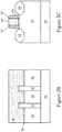
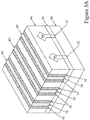
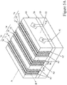
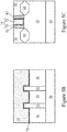
- Figures 1A through 5C illustrate intermediate stages in the manufacturing of FinFETs, in accordance with some embodiments.
- Figures 1A , 2A , 3A , 4A , and 5A are three-dimensional views.
- Figures 1B , 2B , 3B , 4B , and 5B are cross-sectional views shown along a longitudinal axis of the FinFETs, e.g., perpendicular to the direction of current flow between the source/drain regions of the FinFETs, and are shown for a single FinFET.
- Figures 1C , 2C , 3C , 4C , and 5C are cross-sectional views shown along a latitudinal axis of the FinFETs, e.g., parallel to the direction of current flow between the source/drain regions of the FinFETs, and are shown for a single FinFET.
- Figure 2D is a cross-sectional view shown along a longitudinal axis of the FinFETs, through source/drain regions of the FinFETs.
- Some embodiments discussed herein are discussed in the context of FinFETs formed using a gate-last process. In other embodiments, a gate-first process may be used. Also, some embodiments contemplate aspects used in planar devices, such as planar FETs.
- a substrate 50 is provided.
- the substrate 50 may be a semiconductor substrate, such as a bulk semiconductor, a semiconductor-on-insulator (SOI) substrate, a strained SOI substrate, a silicon germanium on insulator substrate, or the like, which may be doped (e.g., with a p-type or an n-type dopant) or undoped.
- the substrate 50 may be a wafer, such as a silicon wafer. Other substrates, such as a multi-layered or gradient substrate may also be used.
- One region of the substrate 50 is illustrated, which can be for forming n-type devices (such as NMOS transistors, e.g., n-type FinFETs) or for forming p-type devices (such as PMOS transistors, e.g., p-type FinFETs).
- the substrate 50 may include multiple, physically separated regions, in which any number of device features (e.g., other active devices, doped regions, isolation structures, etc.) may be formed.
- fins 52 are formed extending from the substrate 50.
- the fins 52 are semiconductor strips.
- the fins 52 are an epitaxially grown semiconductor material, different from the material of the substrate 50.
- the fins 52 may be formed from silicon, silicon germanium (Si x Ge 1-x , where x can be in the range of 0 to 1), silicon carbide, pure or substantially pure germanium, a III-V compound semiconductor, a II-VI compound semiconductor, or the like.
- the available materials for forming a III-V compound semiconductor include, but are not limited to, InAs, AlAs, GaAs, InP, GaN, InGaAs, InAlAs, GaSb, AlSb, A1P, GaP, and the like.
- the fins 52 are formed by epitaxially growing a layer of the semiconductor material on the substrate 50, and then etching trenches 54 in the semiconductor material, with the fins 52 being formed from portions of the semiconductor material that remain unremoved.
- the etching may be any acceptable etch process, such as a reactive ion etch (RIE), neutral beam etch (NBE), the like, or a combination thereof.
- RIE reactive ion etch
- NBE neutral beam etch
- the etch may be anisotropic.
- the fins 52 are the same material as the substrate 50, and are formed by etching trenches in the substrate 50. As discussed below, the fins 52 are used to form channel regions of FinFETs. Although only two fins 52 are illustrated, it should be appreciated that any number of fins 52 may be formed.
- the fins 52 may be patterned by any suitable method.
- the fins 52 may be patterned using one or more photolithography processes, including double-patterning or multi-patterning processes.
- double-patterning or multi-patterning processes combine photolithography and self-aligned processes, allowing patterns to be created that have, for example, pitches smaller than what is otherwise obtainable using a single, direct photolithography process.
- a sacrificial layer is formed over a substrate and patterned using a photolithography process. Spacers are formed alongside the patterned sacrificial layer using a self-aligned process. The sacrificial layer is then removed, and the remaining spacers may then be used to pattern the fins.
- the processes and materials described above to form the fins 52 are merely example processes, and are not meant to be the only embodiments. Rather, any suitable process through which the fins 52 may be formed may be utilized and any suitable process, including any number of masking and removal steps may be used. Once formed, these fins 52 may be used, as discussed below, to form the channel regions and source/drain (S/D) regions of a plurality of FinFET transistors.
- S/D source/drain
- the fins 52 are formed to a width W 1 at the surface of the substrate 50.
- the width W 1 is in the range of about 6 nm to about 600 nm.
- the fins 52 are spaced apart from each other by a distance D 1 . By spacing the fins 52 in such a fashion, the fins 52 may each form a separate channel region while still being close enough to share a common gate.
- the distance D 1 is selected in such a way as to help reduce the contact resistance (R c ) of subsequently formed contacts to the gate of the FinFETs.
- the distance D 1 is large, such as in the range of about 22 nm to about 800 nm. In some embodiments, the distance D 1 is small, such as in the range of about 22 nm to about 200 nm.
- shallow trench isolation (STI) regions 56 are formed between the fins 52.
- the STI regions 56 may be formed by filling the trenches 54 with a dielectric material and recessing the dielectric material in the trenches 54 to form the STI regions 56.
- the dielectric material may be an oxide material, a high-density plasma (HDP) oxide, or the like.
- the dielectric material may be formed, after an optional cleaning and lining of the trenches 54, using a chemical vapor deposition (CVD) method, a high density plasma CVD method, or other suitable method of formation as is known in the art.
- CVD chemical vapor deposition
- the trenches 54 may be filled by overfilling the trenches 54 and the substrate 50 with the dielectric material and then removing the excess material outside of the trenches 54 and the fins 52 through a suitable process such as chemical mechanical polishing (CMP), an etch, a combination thereof, or the like.
- CMP chemical mechanical polishing
- the removal process removes dielectric material overlying the fins 52, so that top surfaces of the fins 52 are exposed.
- the dielectric material may then be recessed from the top surfaces of the fins 52.
- the recessing may be performed to expose at least a portion of the sidewalls of the fins 52 adjacent to the top surfaces of the fins 52.
- the dielectric material may be recessed using a wet etch by dipping the top surfaces of the fins 52 into an etchant such as HF, although other etchants, such as H 2 , and other methods, such as a reactive ion etch, a dry etch with etchants such as NH 3 /NF 3 , chemical oxide removal, or dry chemical clean, may be used.
- the dielectric material is recessed such that the exposed portions of the fins 52 have a first height H 1 .
- the first height H 1 is in the range of about 40 ⁇ to about 100 ⁇ . Additionally, the recessing may also remove any leftover dielectric material located over the fins 52, exposing the fins 52 for further processing.
- steps described above may be only part of the overall process flow used to fill and recess the dielectric material.
- lining steps, cleaning steps, annealing steps, gap filling steps, combinations of these, and the like may also be utilized to form and fill the trenches with the dielectric material. All of the potential process steps are fully intended to be included within the scope of the present embodiments.
- dummy gate dielectrics 58 and dummy gate electrodes 60 are formed over each of the fins 52.
- a dummy gate dielectric layer is formed by thermal oxidation, chemical vapor deposition, sputtering, or any other methods known and used in the art for forming dielectric layers.
- the dummy gate dielectric layer thickness on the top of the fins 52 may be different from the dummy gate dielectric layer thickness on the sidewalls of the fins 52.
- the dummy gate dielectric layer may comprise a material such as silicon dioxide or silicon oxynitride with a thickness of between about 3 ⁇ and about 100 ⁇ , such as about 10 ⁇ .
- the dummy gate dielectric layer may be formed from a high permittivity (high-k) material (e.g., with a relative permittivity greater than about 5) such as lanthanum oxide (La 2 O 3 ), aluminum oxide (Al 2 O 3 ), hafnium oxide (HfO 2 ), hafnium oxynitride (HfON), or zirconium oxide (ZrO 2 ), or combinations thereof, with an equivalent oxide thickness of between about 0.5 ⁇ and about 100 ⁇ , such as about 10 ⁇ or less. Additionally, any combination of silicon dioxide, silicon oxynitride, and/or high-k materials may also be used for the dummy gate dielectric layer.
- the dummy gate electrode layer is then formed on the dummy gate dielectric layer.
- the dummy gate electrode layer may be formed from a conductive material such as polycrystalline-silicon (polysilicon), e.g., a dummy polysilicon (DPO), poly-crystalline silicon-germanium (poly-SiGe), metallic nitrides, metallic silicides, metallic oxides, metals, or the like, including for example W, Al, Cu, AlCu, W, Ti, TiAIN, TaC, TaCN, TaSiN, Mn, Zr, TiN, Ta, TaN, Co, Ni, combinations of these, or the like.
- a conductive material such as polycrystalline-silicon (polysilicon), e.g., a dummy polysilicon (DPO), poly-crystalline silicon-germanium (poly-SiGe), metallic nitrides, metallic silicides, metallic oxides, metals, or the like, including for example W, Al, Cu
- the dummy date electrode layer may be formed by a deposition process such as physical vapor deposition (PVD), chemical vapor deposition (CVD), sputter deposition, or the like.
- the thickness of the dummy gate electrode layer may be between about 5 ⁇ and about 200 ⁇ .
- the top surface of the dummy gate electrode layer may have a non-planar top surface, and may be planarized prior to patterning of the dummy gate electrode layer or performing the gate etching process. Ions may or may not be introduced into the dummy gate electrode layer at this point. Ions may be introduced, for example, by ion implantation techniques.
- the dummy gate electrode layer and dummy gate dielectric layer are then patterned, such as by acceptable photolithography and etching processes, with remaining portions of the dummy gate dielectric layer and dummy gate electrode layer, respectively, forming the dummy gate dielectrics 58 and dummy gate electrodes 60 (collectively "dummy gates").
- the dummy gates define multiple channel regions located on each side of the fins 52 beneath the dummy gate dielectric layer.
- the dummy gates may be formed by depositing and patterning a gate mask on the dummy gate electrode layer using, for example, any suitable deposition and photolithography techniques.
- the gate mask may incorporate any suitable masking and sacrificial materials, such as (but not limited to) silicon oxide, silicon oxynitride, SiCON, SiC, SiOC, and/or silicon nitride and may be deposited to a thickness of between about 5 ⁇ and about 200 A.
- the dummy gate electrode layer and the dummy gate dielectric layer may be etched using a dry etching process to form the patterned dummy gates.
- gate spacers 62 are formed on opposing sides of the dummy gate electrodes 60, over each of the fins 52.
- the gate spacers 62 are formed, for example, by blanket depositing a spacer layer on the previously formed structure.
- the spacer layer may comprise SiCON, SiN, oxynitride, SiC, SiON, SiOC, oxide, or the like and may be formed by any suitable methods to form such a layer, such as chemical vapor deposition (CVD), plasma enhanced chemical vapor deposition (PECVD), sputter, and any other suitable methods.
- the spacer layer may comprise a different material with different etch characteristics or the same material as the dielectric material within the STI regions 56.
- the spacer layer is then patterned, such as by one or more etches to remove horizontal portions of the spacer layer, with remaining vertical portions of the spacer layer forming the gate spacers 62.
- a removal of portions of the fins 52 not protected by the dummy gates and the gate spacers 62 may be removed using a reactive ion etch (RIE) using the dummy gates and the gate spacers 62 as hardmasks, or by using any other suitable removal process.
- RIE reactive ion etch
- the removal process may be continued until the fins 52 are either planar with or below the surface of the STI regions 56.
- Epitaxial source/drain regions 64 are formed in the fins 52, such that each dummy gate electrode 60 is laterally disposed between respective neighboring pairs of the epitaxial source/drain regions 64.
- the epitaxial source/drain regions 64 exert stress in what will be the channel regions of the resulting FinFETs, thereby improving performance.
- the gate spacers 62 separate the epitaxial source/drain regions 64 from the dummy gate electrodes 60 by an appropriate lateral distance so that the epitaxial source/drain regions 64 do not short out subsequently formed gates of the resulting FinFETs.
- the epitaxial source/drain regions 64 are formed by etching recesses in the fins 52.
- the epitaxial source/drain regions 64 in the region are epitaxially grown in the recesses.
- the epitaxial source/drain regions 64 may include any acceptable material, such as appropriate for n-type or p-type FinFETs.
- the epitaxial source/drain regions 64 may include materials exerting a tensile strain in the channel region of the fins 52, such as silicon, SiC, SiCP, SiP, or the like.
- the epitaxial source/drain regions 64 may include materials exerting a compressive strain in the channel region of the fins 52, such as SiGe, SiGeB, Ge, GeSn, or the like.
- the epitaxial source/drain regions 64 may have surfaces raised from respective surfaces of the fins 52 and may have facets.
- the source/drain regions 64 may be regrown with a material, such as silicon, silicon germanium, silicon phosphorous, which has a different lattice constant than the channel regions.
- the epitaxial growth process may use precursors such as silane, dichlorosilane, germane, or the like, and may continue for between about 5 minutes and about 120 minutes, such as about 30 minutes.
- the source/drain regions 64 may comprise materials such as GaAs, GaP, GaN, InP, InAs, InSb, GaAsP, AlGaN, AlInAs, AlGaAs, GaInAs, GaInP, and/or GaInAsP, combinations thereof, or the like.
- dopants may be implanted into the source/drain regions 64 by implanting appropriate dopants to complement the dopants in the fins 52.
- p-type dopants such as boron, gallium, indium, or the like may be implanted to form a PMOS device.
- n-type dopants such as phosphorous, arsenic, antimony, or the like may be implanted to form an NMOS device.
- These dopants may be implanted using the dummy gates and the gate spacers 62 as masks. However, any other suitable processes, steps, or the like may be used to implant the dopants.
- a plurality of implantation processes may be performed using various combinations of spacers and liners to form source/drain regions having a specific shape or characteristic suitable for a particular purpose. Any of these processes may be used to implant the dopants, and the above description is not meant to limit the present embodiments to the steps presented above.
- upper surfaces of the epitaxial source/drain regions 64 have facets which expand laterally outward beyond sidewalls of the fins 52.
- adjacent epitaxial source/drain regions 64 remain separated after the epitaxy process is completed.
- these facets cause adjacent epitaxial source/drain regions 64 of a same FinFET to merge.
- an inter-layer dielectric (ILD) 66 (e.g., ILD0 layer) is deposited over the substrate 50.
- the ILD 66 may be formed of a dielectric material, and may be deposited by any suitable method, such as CVD, PECVD, or flowable CVD (FCVD).
- Dielectric materials may include silicon oxide (SiO2), Phospho-Silicate Glass (PSG), Boro-Silicate Glass (BSG), Boron-Doped Phospho-Silicate Glass (BPSG), undoped Silicate Glass (USG), or the like. Other insulation materials formed by any acceptable process may be used.
- a contact etch stop layer is disposed between the ILD 66 and the epitaxial source/drain regions 64, the gate spacers 62, and the dummy gate electrodes 60.
- the contact etch stop layer may include a dielectric material, such as silicon nitride, silicon oxide, silicon oxynitride, or the like, having a different etch rate than the material of the ILD 66 and may be deposited within a deposition chamber using, for example, one or more of a chemical vapor deposition (CVD), an atomic layer deposition (ALD) process, a plasma enhanced chemical vapor deposition (PECVD), a low pressure chemical vapor deposition (LPCVD), or the like.
- CVD chemical vapor deposition
- ALD atomic layer deposition
- PECVD plasma enhanced chemical vapor deposition
- LPCVD low pressure chemical vapor deposition
- the ILD 66 may be annealed using, e.g., a first annealing process.
- the first annealing process may be a thermal anneal in which the substrate 50 and the ILD 66 are heated, e.g., in a furnace, in an inert atmosphere.
- the first anneal process may be performed at a temperature of between about 200 °C and about 1000 °C, such as about 500 °C, and may be continued for a time of between about 60 s and about 360 min, such as about 240 min.
- a planarization process such as a CMP, is performed to level the top surface of the ILD 66 with the top surfaces of the dummy gate electrodes 60 and the gate spacers 62.
- the dummy gate electrodes 60 and dummy gate dielectrics 58 are removed in one or more etching step(s), e.g., a wet etch process, so that recesses 68 are formed. Each recess 68 exposes a channel region of a respective fin 52. Each channel region is laterally disposed between neighboring pairs of the epitaxial source/drain regions 64.
- the dummy gate dielectrics 58 may be used as etch stop layers when the dummy gate electrodes 60 are etched. The dummy gate dielectrics 58 may then be optionally removed after the removal of the dummy gate electrodes 60.
- gate dielectrics 70 and gate electrodes 72 are formed for replacement gates.
- the replacement gates may include, for example, a gate dielectric, one or more conductive barrier layers, one or more work function layers, and a conductive fill material.
- the gate dielectrics 70 are conformally deposited in the recesses 68, such as on the top surfaces and the sidewalls of the fins 52 and on sidewalls of the gate spacers 62.
- the gate dielectrics 70 may also be formed on top surfaces of the ILD 66.
- the gate dielectrics 70 include silicon oxide, silicon nitride, or multilayers thereof.
- the gate dielectrics 70 include a high-k dielectric material, and in these embodiments, the gate dielectrics 70 may have a k value greater than about 7.0, and may include a metal oxide or a silicate of Hf, Al, Zr, La, Mg, Ba, Ti, Pb, and combinations thereof.
- the high-k gate dielectric includes materials such as HfO 2 , ZrO 2 , HfZrO x , HfSiO x , HfSiON, ZrSiOx, HfZrSiOx, Al 2 O 3 , HfA1O x , HfAIN, ZrA1O x , La 2 O 3 , TiO 2 , Yb 2 O 3 , or the like and may be a single layer or a composite layer that is formed using a deposition process such as atomic layer deposition. However, any suitable materials and any suitable processes may be used to form the high-k gate dielectric.
- the formation methods of the gate dielectrics 70 may include Molecular-Beam Deposition (MBD), atomic layer deposition, PECVD, and the like.
- the gate dielectrics 70 include a material of the dummy gate dielectrics 58 (e.g., SiO 2 ).
- the gate electrodes 72 are deposited over the gate dielectrics 70, respectively, and fill the remaining portions of the recesses 68.
- the gate electrodes 72 may include a metal-containing material such as TiN, TiO, TaN, TaC, Co, Ru, Al, W, combinations thereof, or multi-layers thereof.
- the gate electrodes 72 may be formed by a deposition process such as atomic layer deposition (ALD).
- the gate electrodes 72 may include any number of liner layers, work function tuning layers, and fill materials.
- one or more diffusion barrier layers and one or more work function tuning layers may be formed as a plurality of stacked layers.
- the barrier layers may be formed as a layer of titanium nitride (TiN) which may (or may not) be doped with silicon.
- the work function tuning layer in the case of a p-type FinFET, may be formed with a respective gate electrode 72 as a stacked layer including Ti, Al, TiAl, TiAIN, Ta, TaN, TiAlC, TaA1CSi, TaAlC, TiSiN, or the like.
- the work function tuning layer may be formed with a respective gate electrode 72 as a stacked layer including TiN, TaN, TiAl, W, Ta, Ni, Pt, or the like.
- a barrier layer e.g., another TiN layer may be formed.
- the conductive fill material may be formed from a material such as tungsten, cobalt, copper, ruthenium, aluminum, or the like.
- the conductive fill material is deposited over the gate dielectric, the one or more conductive barrier layers, and the one or more work function tuning layers such that the remaining spaces between respective spacers 62 of a respective gate electrode 72 are filled or over-filled.
- a planarization process such as a CMP, may be performed to remove the excess portions of the gate dielectrics 70 and the material of the gate electrodes 72, which excess portions are over the top surface of the ILD 66.
- the remaining portions of material of the gate electrodes 72 and the gate dielectrics 70 thus form replacement gates of the resulting FinFETs.
- the gate electrodes 72 and the gate dielectrics 70 may be collectively referred to as gate stacks 74.
- the gate stacks 74 extend along sidewalls of a channel region of the fins 52.
- the ILD 66 may again be annealed using, e.g. a second annealing process.
- the second annealing process may be a thermal anneal in which the substrate 50 and the ILD 66 are heated, e.g., in a furnace, in an inert atmosphere.
- the second annealing process may be performed at a temperature of between about 200 °C and about 1000 °C, such as about 500 °C, and may be continued for a time of between about 60 s and about 360 min, such as about 240 min.
- the gate stacks 74 After formation, the gate stacks 74 have a width W 2 . In some embodiments, the width W 2 is in the range of about 6 nm to about 300 nm. As discussed further below, the distance D 1 between the fins 52 (see Figure 1A ) is selected according to the width W 2 of the gate stacks 74 that are formed.
- Figure 5A further illustrates reference cross-sections that are used in later figures.
- Cross-section A-A' is between fins 52 and parallel to a longitudinal axis of the fins 52.
- Cross-section B-B' is perpendicular to cross-section A-A' and is along a longitudinal axis of a gate stack 74 and in a direction, for example, perpendicular to the current flow between the epitaxial source/drain regions 64 of the FinFETs.
- Cross-section C-C' is parallel to cross-section B-B' and extends through the epitaxial source/drain regions 64 of the FinFETs. Subsequent figures refer to these reference cross-sections for clarity.
- Figures 6A-19C and 21A-22C represent cross-sectional views that are taken through an intermediate structure formed using the intermediate steps associated with the respective figures.
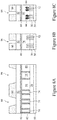
- Figures 6A , 7A , 8A , 9A , 10A , 11A , 12A , 13A , 14A , 15A , 16A , 17A , 18A , 19A , 21A , and 22A ("the 'A' cross-sectional views") are taken along line A-A' of Figure 5A except with a different number of gate stacks 74.
- Figures 6B , 7B , 8B , 9B , 10B , 11B , 12B , 13B , 14B , 15B , 16B , 17B , 18B , 19B , 21B , and 22B are views taken along line B-B' of Figure 5A except with a different number of fins 52.
- Figures 6C , 7C , 8C , 9C , 10C , 11C , 12C , 13C , 14C , 15C , 16C , 17C , 18C , 19C , 21C , and 22C are views taken along line C-C' of Figure 5A except with a different number of fins 52.
- the cross-sections A-A', B-B', and C-C' illustrated in Figure 5A are shown on an example FinFET structure and the cross-section views in Figures 6A-19C and 21A-22C are arranged differently relative to each other. These relative arrangements of these cross-sectional views are shown in the Figures 6A-19C and 21A-22C .
- the "A" cross-sectional views are taken through line A-A' illustrated in association with the "B” and “C” cross-sectional views to show a series of gate structures in a direction parallel to the fins of the FinFETS being formed.
- the "B” cross-sectional views are taken through line B-B' illustrated in association with the "A” and “C” cross-sectional views to show a gate structure of the series of gate structures in an area of a cut metal gate (CMG) of the respective intermediate structures in a direction perpendicular to the fins of the FinFETS being formed.
- CMG cut metal gate
- the "C” cross-sectional views are taken through line C-C' illustrated in the associated "A” and "B” cross-sectional views to show an area of an ILD0/EPI interface associated with the cut metal gate (CMG) of the respective intermediate structures in a direction perpendicular to the fins of the FinFETS being formed.
- CMG cut metal gate
- Figures 6A-16C illustrate intermediate stages in the manufacturing of FinFETs having a cut metal gate, in accordance with some embodiments.
- Figures 6A-6C illustrate an intermediate structure similar to the intermediate structure of Figures 5A-5C and at a same step in the fabrication process of the FinFETs.
- four gate stacks 74 are shown on the substrate 50, and in Figures 6B and 6C , two pairs of the fins 52 are shown in the corresponding views.
- the four gate stacks 74 are shown in a same area of the substrate 50, one of ordinary skill in the art will understand that these gate stacks 74 may be physically separated from each other and any number of device features (e.g., other active devices, doped regions, isolation structures, etc.) may be disposed between the gate stacks 74.
- the rightmost gate 74 in Figures 6A-16C may be in an input/output region of the substrate 50 while the three leftmost gate stacks 74 of Figures 6A-16C may be in a memory area of the substrate, such as a static random access memory (SRAM) area.
- the gate stacks 74 may have different channel lengths.
- the rightmost gate stack 74 is wider than the other illustrated gate stacks 74, and thus, the rightmost gate stack 74 may have a longer channel length than the other illustrated gate stacks 74.
- Figures 7A-7C illustrate some initial steps in forming a "cut metal gate” (CMG) through one or more of the gate stacks 74 of the intermediate structure illustrated in Figures 6A-6C .
- CMG cut metal gate
- a first layer in the series of masking layers may be an etch stop layer 80.
- the etch stop layer 80 may be formed over the planarized surfaces of the gate stacks 74 and the ILD 66 by depositing a material such as Si, TiN, SiN, SiO2, combinations thereof, or the like using a deposition method such as atomic layer deposition (ALD), plasma enhanced chemical vapor deposition (PECVD), chemical vapor deposition (CVD), or the like.
- ALD atomic layer deposition
- PECVD plasma enhanced chemical vapor deposition
- CVD chemical vapor deposition
- any suitable materials and any suitable methods may be used to form the etch stop layer 80.
- a hard mask layer 82 may be deposited over the etch stop layer 80 as a second layer of the series of masking layers.
- the hard mask layer 82 is formed over the etch stop layer 80 from a second hard mask material such as SiN, SiO2, combinations thereof, or the like.
- the second hard mask material used to form the hard mask layer 82 is different from the first hard mask material used to form the etch stop layer 80.
- the etch stop layer 80 may serve as an etch stop of a subsequent patterning of the hard mask layer 82.
- the hard mask layer 82 may be placed over the etch stop layer 80 using a deposition method such as atomic layer deposition (ALD), plasma enhanced chemical vapor deposition (PECVD), chemical vapor deposition (CVD), or the like.
- ALD atomic layer deposition
- PECVD plasma enhanced chemical vapor deposition
- CVD chemical vapor deposition
- any suitable material and process of formation may be used for the hard mask layer 82 in the first series of hard masking layers.
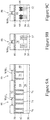
- Figures 8A-8C illustrate a deposition and patterning process to form openings 84 through a photo resist layer 86 deposited over the hard mask layer 82.
- the photo resist layer 86 may be deposited over the hard mask layer 82 as a third layer of the series of masking layers.
- the photo resist layer 86 may be deposited using any suitable deposition process, may be formed to any suitable thickness, and may be patterned using any suitable photo lithography method to form the openings 84 through the photo resist layer 86 and to expose surfaces of the hard mask layer 82 of the first series of masking layers in areas overlying one or more of the gate stacks 74.
- Figures 9A-9C illustrate a transferring of the pattern of the photo resist layer 86 of Figures 8A-8C into the hard mask layer 82 using a first etchant to form a pattern of openings 88 through the hard mask layer 82.
- the first etchant may use reactant gases having a greater etching selectivity for the hard mask material used to form the hard mask layer 82 than the hard mask material used to form the etch stop layer 80.
- the etch stop layer 80 serves as a etch stop layer and areas of the etch stop layer 80 overlying the one or more of the gate stacks 74 are exposed through the openings 88.
- the etching process may be performed using, for example, carbon-and-fluorine-containing gases such as CF 4 , CH 2 F 2 , CHF 3 , or the like.
- carbon-and-fluorine-containing gases such as CF 4 , CH 2 F 2 , CHF 3 , or the like.
- any suitable gas may be used for the first etchant.
- the openings 88 in Figure 9A may be formed to one or more widths W88X of between about 5 nm and about 500 nm, such as about 100 nm and in Figures 9B and 9C may be formed to one or more widths W88Y of between about 5 nm and about 50 nm, such as about 30 nm.
- any suitable widths may be used for the openings 88.
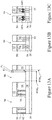
- Figures 10A-10C illustrate a narrowing of the openings 88 to form narrow openings 90 via a re-deposition of the second hard mask material as a blanket mask layer 92.
- the blanket mask layer 92 may be formed, for example, through a conformal deposition process such as chemical vapor deposition (CVD) or atomic layer deposition (ALD) such that the blanket mask layer 92 lines the exposed surfaces of the etch stop layer 80, lines the exposed surfaces of the hard mask layer 82, and lines the sidewalls of the openings 88 through the hard mask layer 82.
- the blanket mask layer 92 may be formed of the same hard mask material (e.g., silicon nitride) used to form the hard mask layer 82.
- the blanket mask layer 92 is formed to a highly uniform thickness of between about 10 ⁇ and about 100 ⁇ , such as about 50 ⁇ .
- the narrow openings 90 in Figure 10A may be formed to one or more widths W90X of between about 5 nm and about 500 nm, such as about 100 nm and in Figures 10B and 10C may be formed to one or more widths W90Y of between about 5 nm and about 50 nm, such as about 30 nm.
- any suitable widths may be used for the narrow openings 90.
- Figures 11A-11C illustrate an anisotropic etching process performed to remove portions of the blanket mask layer 92 lining the bottoms of the narrow openings 90.
- the etch stop layer 80 serves as an etch stop layer during the anisotropic etching process. As such, at least portions of the areas of the etch stop layer 80 overlying the one or more of the gate stacks 74 are re-exposed through the narrow openings 90.
- the anisotropic etch the horizontal portions of the blanket mask layer 92 lining the bottoms of the narrow openings 90 are removed whereas the remaining vertical portions on the sidewalls of the narrow openings 90 remain intact.
- the vertical portions on the sidewalls of the narrow openings 90 form full rings having dimensions corresponding to the widths W90X and W90Y as illustrated in Figures 10A-10C and corresponding to the cut lines A-A', B-B', C-C' as illustrated in Figures 6A-6C .
- the anisotropic etching process may be performed to remove the blanket mask layer 92 lining the bottoms of the narrow openings 90 using, for example, carbon-and-fluorine-containing gases such as CF4, CH2F2, CHF3, or the like. However, any suitable gases may be used for the anisotropic etching process.
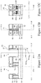
- FIGs 12A-12C illustrate a cut-metal gate (CMG) etching process performed to remove the exposed portions of the areas of the etch stop layer 80 and to remove the one or more target portions of the gate stacks 74 (may be referred to as the cut metal gate region of the gate stacks 74), the associated gate spacers 62 and portions of the ILD 66 in order to form CMG trenches 94.
- This CMG etching process separates the one or more target portions of the gate stacks 74 into first metal gate sections 74a and second metal gate sections 74b, effectively "cutting" the first sections from the second sections as shown in Figure 12B .
- the CMG etching process also separates the one or more target portions of the ILD 66 of the source/drain regions into first ILD sections 66a and second ILD sections 66b, effectively "cutting" the first sections from the second sections as shown in Figure 12C .
- the CMG etching process comprises a dry etching using chlorinecontaining or fluorine-containing gases, such as Cl 2 , NF 3 , SiCl 4 , BCl 3 , O 2 , N 2 , H 2 , Ar, combinations thereof, or the like.
- any suitable dry etching gases may be used for the CMG etching process.
- the CMG trenches 94 are formed to a first depth P1 in a first portion of the CMG trenches 94 and are formed to a second depth P2 in a second portion of the CMG trenches 94.
- the first portions of the CMG trenches 94 are formed by removing the materials of the target portions of the gate stacks 74, removing the materials of the target portions of the gate spacers 62, and removing the materials of portions of the ILD 66 underlying the target portions of the gate stacks 74 and the target portions of the gate spacers 62.
- the first portions of the CMG trenches 94 are formed to a first width W94X1 corresponding to the widths of the target gates of the gate stacks 74 and corresponding to the thicknesses of the gate spacers 62 in the ILD 66.
- the second portions of the CMG trenches 94 are formed by removing the materials of the blanket mask layer 92 formed along the vertical sidewalls of the openings 88 through the hard mask layer 82 and by removing the materials of the portions of the ILD 66 underlying the blanket mask layer 92 formed along the vertical sidewalls of the openings 88 through the hard mask layer 82. As such, the second portions of the CMG trenches 94 are formed to a second width W94X2 corresponding to the widths of the openings W88X in the hard mask layer 82.
- Figure 12B taken along the cut line B-B' near or at the center of the CMG trenches 94, illustrates the CMG trenches 94 are formed to the first depth P1 at which the target gate stacks 74 are fully separated (i.e., "cut") into their first sections 74a and second sections 74b.
- Figure 12C taken along the cut line C-C' near or at an area of the source/drain regions 64 of the CMG trenches 94, illustrates the CMG trenches 94 are formed to the second depth P2 at which a portion of the ILD 66 remains above the isolation regions 56 separating a portion of the fins 52 of adjacent devices.
- a residual byproduct material 96 (e.g., a polymer) may be formed as a byproduct of reactions between the materials of the hard mask layer 82, the materials of the etch stop layer 80, the materials of the target gate stacks 74, the materials of the gate spacers 62, the materials of the ILD 66, and the reactant gases during the CMG etching process.
- the residual byproduct material 96 may be formed over the hard mask layer 82 and along sidewalls of the CMG trenches 94.
- Figures 13A-13C illustrate a removal of the residual byproduct material 96.
- a polymer removal process is performed to remove any residual polymer byproduct 96.
- a non-plasma recipe with HF/NH3 gas may be used to remove the polymer material.
- the non-plasma recipe with HF/NH3 gas has low selectivity to metal and may be adjusted to have different selectivity to SiN by adjusting pressures and temperatures during removal of the polymer byproduct 96.
- a wet clean may be performed to ensure a clean surface of the CMG trenches 94 for further processing.
- a solution such as an SC-1 or SC-2 cleaning solution may be utilized for the wet clean process.
- other solutions such as a mixture of H 2 SO 4 and H 2 O 2 (known as SPM), or a solution of hydrogen fluoride (HF), may also be utilized.
- SPM H 2 SO 4 and H 2 O 2
- HF hydrogen fluoride
- any suitable solution or any suitable process may be used for the wet clean process and are fully intended to be included within the scope of the embodiments.
- the CMG trenches 94 may be formed to a first depth P1 of between about 50 nm and about 300 nm, and formed to a first width W94 X1 of between about 5 nm and about 500 nm, such as about 100 nm.
- the CMG trenches 94 may also be formed to a second depth P2 of between about 48 nm and about 298 nm, such as about 198 nm, and formed to a second width W94 X2 of between about 1 nm and about 10 nm, such as about 4 nm.
- any suitable depths and any suitable widths may be used for the first depth P1 and the second depth P2 of the CMG trenches 94 and any suitable widths may be used for the first width W94 X1 and the second width W94 X2 of the CMG trenches 94.
- the CMG trenches 94 may have, for example, a U, V, or square shape when viewed in the cross-sections in Figures 13B and 13C and subsequent figures in these same cross sections.
- the CMG trenches 94 have a square shape though other shapes are possible and are fully intended to be included within the scope of the embodiments (see, e.g., Figs 21A-22C ).
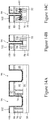
- Figures 14A-14C illustrate a deposition of a barrier layer 100 over the structure of Figures 13A-13C .
- the barrier layer 100 can help to prevent the diffusion of the materials of CMG trenches 94 into the gate stacks 74 during subsequent processing.
- the barrier layer 100 may comprise silicon nitride or the like.
- the barrier layer 100 may, for example, have a dielectric constant of in a range from about 6.5 to about 8.
- the barrier layer 100 may be deposited conformally using a deposition process such as ALD.
- the barrier layer 100 may be deposited to a thickness of about 1 nm to about 15 nm, such as about 5 nm, on each side of the CMG trenches 94.
- the barrier layer 100 is a silicon nitride layer deposited by a plasma enhanced atomic layer deposition (PEALD) process.
- the PEALD process may be performed at a temperature in a range from 300 °C to about 600 °C.
- the PEALD process forming the silicon nitride layer may include precursors of diiodosilane (SiH 2 I 2 ) and NH 3 .
- Figures 14A-14C further illustrate an oxygen blocking layer 102 deposited conformally over the barrier layer 100.
- the oxygen blocking layer 102 may be formed as an amorphous silicon material layer, or the like.
- the silicon layer102 may be deposited to a thickness in the range of about 2 ⁇ to about 10 ⁇ , such as about 5 ⁇ , on each side of the CMG trenches 94.
- the silicon layer 102 is deposited to a thickness of less than about 5 ⁇ .
- the silicon layer 102 may be depositing conformally using a deposition process such as CVD.
- the silicon layer 102 acts as a barrier to oxidation of the underlying barrier layer 100 and the gate stacks 74.
- the oxygen blocking layer 102 may be formed of other suitable materials that have low-k values and will act as a barrier to oxidation of the underlying barrier layer 100 and the gate stacks 74.
- the silicon layer 102 is deposited by CVD in a furnace at a temperature in a range from about 350 to about 450 °C, at a pressure of about 1 to about 3 torr, with a disilane flow of about 0.3 to about 0.5 standard liters per minute (slm) and an N2 carrier flow of about 0 to 1 slm.
- the silicon layer 102 is deposited by PEALD in a single wafer chamber at a temperature in a range from about 300 °C to about 600 °C, at a pressure of about 10 to about 20 torr, with precursor diiodosilane (SiH 2 I 2 ) and a N 2 flow of about 200 to about 2000 slm, such as 800 slm, at a radio frequency of about 600 to about 800 watts, for about 0.2 to about 10 minutes, such as one minute.
- precursor diiodosilane SiH 2 I 2
- the silicon layer 102 is deposited by PEALD in a furnace at a temperature in a range from about 200 °C to about 500 °C, at a pressure in a range from about 2 to about 5 torr, with precursor N-(diethylaminosilyl)-N-ethylethanamine (C 8 H 22 N 2 Si) and an Ar flow rate in a range from about 0.5 to about 10 slm, such as 2 slm, at a radio frequency of about 15 to 100 watts, and with a time in a range from about 0.2 to about 10 minutes, such as one minute.
- PEALD in a furnace at a temperature in a range from about 200 °C to about 500 °C, at a pressure in a range from about 2 to about 5 torr, with precursor N-(diethylaminosilyl)-N-ethylethanamine (C 8 H 22 N 2 Si) and an Ar flow rate in a range from about 0.5 to about 10 slm,
- an oxidation process is performed to convert at least a portion of the silicon layer 102 into a silicon oxide layer.
- the oxidation process includes an in-situ O 2 purge oxidation method.
- the oxidation process includes an in-situ O 2 soak in a furnace, at a temperature in a range from about 350 °C to 450 °C, at a pressure in a range from about 1 to about 3 torr, with a flow rate of O 2 in a range from about 0.2 to about 10 slm, and for a time in a range from about 2 mins to about 30 mins.
- the silicon layer 102 is formed to have a thickness less than about 5 ⁇ , the oxidation process fully converts the silicon layer 102 to be a silicon oxide layer.
- the oxidation process is performed by breaking the vacuum to expose the silicon layer 102 to ambient atmosphere while the device is in queue for the next stage of processing described with respect to Figures 15A-15C below.
- the combined thickness of any remaining silicon layer 102 and the newly formed silicon oxide layer may have a thickness of about 0.4 nm to about 1.5 nm on each side of the CMG trenches 94.
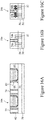
- a fill material 104 is deposited over the oxidized structure of Figures 14A-14C .
- the CMG trenches 94 may be filled with the fill material 104.
- the oxidized silicon layer is shown as being part of the fill material 104 as the material composition may be the same.
- the fill material 104 may be deposited using a deposition process such as PEALD, PECVD, ALD, CVD, or the like.
- the fill material 104 is silicon oxide having a dielectric constant of about 3.5 to about 5. In an embodiment, the fill material 104 may be deposited to overfill the CMG trenches 94 to a level above the top surface of hard mask layer 82.
- the fill material is deposited by PEALD with precursors N-(diethylaminosilyl)-N-ethylethanamine (C 8 H 22 N 2 Si) and O 2 .
- each of the deposition of the barrier layer 100, the deposition of the silicon layer 102, and the oxidation of the silicon layer 102 can be performed in a single chamber. In other embodiments, the deposition of the barrier layer 100 is deposited in a separate chamber.
- each of the deposition of the silicon layer 102, the oxidation of the silicon layer 102, and the deposition of the fill material 104 can be performed in a single chamber.
- the deposition of the barrier layer 100 is performed in a separate chamber.
- the oxidized silicon layer 102 and the fill material 104 are both silicon oxide and are over the barrier layer 100 in the CMG trenches 94.
- FIGS 16A-16C illustrates a planarization of the fill material 104 which may be performed using, for example, a chemical mechanical (CMP) planarization process to remove the excess material of the fill material 104.
- CMP planarization process may continue until the etch stop layer 80 has been fully removed and may continue until top surfaces of the fill material 104, the gate stacks 74, and the respective gate spacers 62 are exposed within a planar surface of the ILD 66.
- CMG plugs 106 are formed from remaining material of the barrier layer 100, the silicon layer 102 (if any), and the fill material 104 disposed within the ILD 66.
- the heights of the gate stacks 74 and the heights of the CMG plugs 106 may be reduced to an overall first height H1 of between about 50 nm and about 120 nm, such as about 100 nm. However, any suitable heights may be used for the gate stacks 74 and the CMG plugs 106.
- Figures 17A-19C illustrate intermediate stages in the manufacturing of FinFETs having a cut metal gate, in accordance with some other embodiments.
- the embodiment in Figures 17A-19C is similar to the embodiment illustrated in Figures 1-16C except that in this embodiment some of an oxygen blocking layer 202 remains unoxidized in the final structure.
- the oxygen blocking layer 202 may be formed thicker than the oxygen blocking layer 102 of the previous embodiment such that the oxidation process does not oxidize the entirety of the oxygen blocking layer 202.
- the oxygen blocking layer 202 may be a silicon layer 202. Details regarding this embodiment that are similar to those for the previously described embodiment will not be repeated herein.
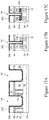
- Figures 17A-17C illustrates an intermediate stage of processing similar to that described in Figures 14A-14C above and the description of forming this intermediate stage of processing is not repeated herein.
- a barrier layer 200 is deposited over the structure of Figures 13A-13C .
- the materials and processes used to form the barrier layer 200 may be similar to the barrier layer 100 described above and the description is not repeated herein.
- Figures 17A-17C further illustrate the silicon layer 202 deposited conformally over the barrier layer 200.
- the silicon layer 202 may be deposited to a thickness in the range of about 5 ⁇ to about 10 ⁇ , on each side of the CMG trenches 94. In the embodiment of Figures 17A-17C , the silicon layer 202 is deposited to a thickness of greater than or equal to about 5 ⁇ .
- the materials and processes used to form the silicon layer 202 may be similar to the silicon layer 102 described above and the description is not repeated herein.
- an oxidation process is performed to convert a portion of the silicon layer 202 into a silicon oxide layer while some of the silicon layer 202 remains.
- the oxidation process may be similar to the oxidation process described above in reference to Figures 14A-14C and the description is not repeated herein. Because the silicon layer 202 is formed thicker in this embodiment, the oxidation process does not convert the entirety of the silicon layer 202 into a silicon oxide layer and some of the silicon layer 202 remains.
- a fill material 204 is deposited over the oxidized structure of Figures 17A-17C .
- the materials and processes used to form the fill material 204 may be similar to the fill material 104 described above and the description is not repeated herein.
- the fill material 204 is planarized using, for example, CMP planarization process to remove the excess material of the fill material 204.
- the CMP planarization process may continue until the etch stop layer 80 has been fully removed and may continue until top surfaces of the fill material 204, the gate stacks 74, and the respective gate spacers 62 are exposed within a planar surface of the ILD 66.
- CMG plugs 206 are formed from remaining material of the barrier layer 200, the silicon layer 202, and the fill material 204 disposed within the ILD 66.
- the heights of the gate stacks 74 and the heights of the CMG plugs 206 may be reduced to an overall height H2 of between about 50 nm and about 120 nm, such as about 100 nm. However, any suitable heights may be used for the gate stacks 74 and the CMG plugs 206.
- Figure 20 illustrates a semiconductor device following additional stages in the manufacturing of FinFETs having a cut metal gate.
- a ILD 76 is deposited over the ILD 66.
- the ILD 76 is a flowable film formed by a flowable CVD method.
- the ILD 76 is formed of a dielectric material such as PSG, BSG, BPSG, USG, or the like, and may be deposited by any suitable method, such as CVD and PECVD.
- gate contacts 78 and source/drain contacts are formed through the ILD 76 and the ILD 66. Openings for the source/drain contacts are formed through the ILD 66 and the ILD 76, and openings for the gate contacts 78 are formed through the ILD 76 (and optionally the gate mask, if formed).
- the gate contacts 78 may include a liner (such as a diffusion barrier layer, an adhesion layer, or the like) and a conductive material. The openings may be formed using acceptable photolithography and etching techniques. The liner and the conductive material are formed in the openings.
- the liner may include titanium, titanium nitride, tantalum, tantalum nitride, or the like.
- the conductive material may be copper, a copper alloy, silver, gold, tungsten, cobalt, aluminum, nickel, or the like.
- the conductive material may be formed by a deposition process such as CVD.
- a planarization process such as a CMP, may be performed to remove excess material from a surface of the ILD 76.
- the remaining liner and conductive material form the source/drain contacts and the gate contacts 78 in the openings.
- An anneal process may be performed to form a silicide at the interface between the epitaxial source/drain regions 64 and the source/drain contacts.
- the source/drain contacts are physically and electrically coupled to the epitaxial source/drain regions 64, and the gate contacts 78 are physically and electrically coupled to the gate electrodes 72.
- the source/drain contacts and the gate contacts 78 may be formed in different processes, or may be formed in the same process.
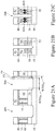
- Figures 21A-22C illustrate intermediate stages in the manufacturing of FinFETs having a cut metal gate, in accordance with some other embodiments.
- the embodiment in in Figures 21A-22C is similar to the embodiments illustrated in Figures 1A-16C and Figures 17A-19C except that in this embodiment the CMG trenches are formed with a U shape. Also, in this embodiment, the trenches may be formed deeper to extend through the isolation regions 56 and partially into the substrate 50. Details regarding this embodiment that are similar to those for the previously described embodiments will not be repeated herein002E
- FIGS 21A-21C illustrates an intermediate stage of processing similar to that described in Figures 13A-13C above and the description of forming this intermediate stage of processing is not repeated herein.
- a cut-metal gate (CMG) etching process is performed to remove the exposed portions of the areas of the etch stop layer 80 and to remove the one or more target portions of the gate stacks 74, the associated gate spacers 62 and portions of the ILD 66 in order to form CMG trenches 300.
- the materials and processes used to form the CMG trenches 300 may be similar to the CMG trenches 94 described above and the description is not repeated herein.
- the etching time to form the CMG trenches 300 may be increased from the previous embodiments to have the CMG trenches 300 formed to greater depth.
- the CMG trenches 300 are formed to a depth P3 in a first portion of the CMG trenches 300 and are formed to a depth P4 in a second portion of the CMG trenches 300.
- the first portions of the CMG trenches 300 are formed by removing the materials of the target portions of the gate stacks 74, removing the materials of the target portions of the gate spacers 62, and removing the materials of portions of the ILD 66 underlying the target portions of the gate stacks 74 and the target portions of the gate spacers 62.
- the first portions of the CMG trenches 300 are formed to a first width W300 X1 corresponding to the widths of the target gates of the gate stacks 74 and corresponding to the thicknesses of the gate spacers 62 in the ILD 66.
- the second portions of the CMG trenches 300 are formed by removing the materials of the blanket mask layer 92 formed along the vertical sidewalls of the openings 88 through the hard mask layer 82 and by removing the materials of the portions of the ILD 66 underlying the blanket mask layer 92 formed along the vertical sidewalls of the openings 88 through the hard mask layer 82. As such, the second portions of the CMG trenches 300 are formed to a second width W300 X2 corresponding to the widths of the openings W88 X in the hard mask layer 82 (see, e.g., Figs.9A-9C ).
- the CMG trenches 300 may be formed to a first depth P3 of between about 150 nm and about 350 nm, and formed to a first width W300 X1 of between about 5 nm and about 25 nm, such as about 10 nm.
- the CMG trenches 300 may also be formed to a second depth P4 of between about 130 nm and about 330 nm, such as about 250 nm, and formed to a second width W300 X2 of between about 2 nm and about 20 nm, such as about 7 nm.
- any suitable depths and any suitable widths may be used for the first depth P3 and the second depth P4 of the CMG trenches 300 and any suitable widths may be used for the first width W300 X1 and the second width W300 X2 of the CMG trenches 94.
- the CMG trenches 300 may have, for example, a U, V, or square shape when viewed in the cross-sections in Figures 21B and 21C and subsequent figures in these same cross sections.
- the CMG trenches 300 have a U shape though other shapes are possible and are fully intended to be included within the scope of the embodiments.
- Figures 22A-22C illustrates subsequent processing performed on the structure in Figures 21A-21C .
- the subsequent processing between Figures 21A-21C and 22A-22C is similar to the process illustrated and described above in Figures 14A-14C and 16A-16C or Figures 17A-17C and 19A-19C and the description is not repeated herein.
- Figures 22A-22C illustrates a barrier layer 302 formed in the CMG trenches 300 and a fill material 304 formed on the barrier layer 302.
- a oxygen blocking layer e.g., silicon layer 102 or 202
- a oxygen blocking layer between the barrier layer 302 and the fill material 304 is possible and fully intended to be included within the scope of this embodiment.
- the barrier layer 302 because the CMG trenches 300 exposed the substrate 50, the barrier layer 302 physically contacts the 50 in the trenches 300.
- the barrier layer 302 may be similar to the barrier layer 100 and the fill material 304 may be similar to the fill material 104. The materials and processes used to form barrier layer 102 and fill material 104 was described above and the description is not repeated herein.
- FIGS 22A-22C further illustrates CMG plugs 306.
- the materials and processes used to form the CMG plugs 306 may be similar to the CMG plugs 106 described above and the description is not repeated herein.
- the heights of the gate stacks 74 and the heights of the CMG plugs 306 may be reduced to an overall first height H3 of between about 50 nm and about 150 nm.
- any suitable heights may be used for the gate stacks 74 and the CMG plugs 306.
- Embodiments may achieve advantages.
- Embodiments include a cut metal gate (CMG) isolation structure formed in a CMG trench that improves the resistive-capacitive delay for the device and without degrading the threshold voltage of the device.
- the CMG isolation structure includes multiple layers with a silicon nitride layer, a silicon layer, and a silicon oxide layer.
- the silicon nitride layer acts as a barrier layer to prevent the diffusion of the materials of the gate stacks into the CMG trenches during subsequent processing.
- the silicon layer acts as a barrier to oxidation of the underlying barrier layer and the gate stacks.
- a silicon oxide layer can be formed on the silicon layer, which reduces the dielectric constant of the CMG isolation structure. Further, by protecting the underlying layers (e.g., the gate stacks) from oxidation, the threshold voltages of the devices can be maintained while utilizing a CMG approach.
Landscapes
- Insulated Gate Type Field-Effect Transistor (AREA)
- Physics & Mathematics (AREA)
- Engineering & Computer Science (AREA)
- Plasma & Fusion (AREA)
- Bipolar Transistors (AREA)
- Thin Film Transistor (AREA)
Abstract
An embodiment includes a method including forming an opening in a cut metal gate region of a metal gate structure of a semiconductor device, conformally depositing a first dielectric layer in the opening, conformally depositing a silicon layer over the first dielectric layer, performing an oxidation process on the silicon layer to form a first silicon oxide layer, filling the opening with a second silicon oxide layer, performing a chemical mechanical polishing on the second silicon oxide layer and the first dielectric layer to form a cut metal gate plug, the chemical mechanical polishing exposing the metal gate structure of the semiconductor device, and forming a first contact to a first portion of the metal gate structure and a second contact to a second portion of the metal gate structure, the first portion and the second portion of the metal gate structure being separated by the cut metal gate plug.
Description
- Semiconductor devices are used in a variety of electronic applications, such as, for example, personal computers, cell phones, digital cameras, and other electronic equipment. Semiconductor devices are typically fabricated by sequentially depositing insulating or dielectric layers, conductive layers, and semiconductor layers of material over a semiconductor substrate, and patterning the various material layers using lithography to form circuit components and elements thereon.
- The semiconductor industry continues to improve the integration density of various electronic components (e.g., transistors, diodes, resistors, capacitors, etc.) by continual reductions in minimum feature size, which allow more components to be integrated into a given area. However, as the minimum features sizes are reduced, additional problems arise that should be addressed.
- Aspects of the present disclosure are best understood from the following detailed description when read with the accompanying figures. It is noted that, in accordance with the standard practice in the industry, various features are not drawn to scale. In fact, the dimensions of the various features may be arbitrarily increased or reduced for clarity of discussion.
-
Figures 1A through 5C illustrate intermediate stages in the manufacturing of FinFETs, in accordance with some embodiments. -
Figures 6A through 16C illustrate intermediate stages in the manufacturing of FinFETs having a cut metal gate, in accordance with some embodiments. -
Figures 17A through 19C illustrate intermediate stages in the manufacturing of FinFETs having a cut metal gate, in accordance with some other embodiments. -
Figure 20 illustrates a semiconductor device following additional stages in the manufacturing of FinFETs having a cut metal gate, in accordance with some embodiments. -
Figures 21A through 22C illustrate intermediate stages in the manufacturing of FinFETs having a cut metal gate, in accordance with some other embodiments. - The following disclosure provides many different embodiments, or examples, for implementing different features of the invention. Specific examples of components and arrangements are described below to simplify the present disclosure. These are, of course, merely examples and are not intended to be limiting. For example, the formation of a first feature over or on a second feature in the description that follows may include embodiments in which the first and second features are formed in direct contact, and may also include embodiments in which additional features may be formed between the first and second features, such that the first and second features may not be in direct contact. In addition, the present disclosure may repeat reference numerals and/or letters in the various examples. This repetition is for the purpose of simplicity and clarity and does not in itself dictate a relationship between the various embodiments and/or configurations discussed.
- Further, spatially relative terms, such as "beneath," "below," "lower," "above," "upper" and the like, may be used herein for ease of description to describe one element or feature's relationship to another element(s) or feature(s) as illustrated in the figures. The spatially relative terms are intended to encompass different orientations of the device in use or operation in addition to the orientation depicted in the figures. The apparatus may be otherwise oriented (rotated 90 degrees or at other orientations) and the spatially relative descriptors used herein may likewise be interpreted accordingly.
- This disclosure relates to semiconductor devices and manufacturing methods thereof. Particular embodiments relate to a semiconductor device comprising a fin field effect transistor (FinFET) with a cut metal gate (CMG) and a method of manufacturing the semiconductor device. Embodiments disclosed herein are directed towards the formation of a plurality of FinFETs within a wafer.
- Embodiments discussed herein may be discussed in a specific context, namely a cut metal gate (CMG) isolation structure formed in a CMG trench that improves the resistive-capacitive delay for the device and without degrading the threshold voltage of the device. In some embodiments, the CMG isolation structure includes multiple layers with a silicon nitride layer, a silicon layer, and a silicon oxide layer. In some embodiments, the silicon nitride layer acts as a barrier layer to prevent the diffusion of the materials of the gate stacks into the CMG trenches during subsequent processing. In some embodiments, the silicon layer acts as a barrier to oxidation of the underlying barrier layer and the gate stacks. Because the silicon layer protects the underlying layers from oxidation, a silicon oxide layer can be formed on the silicon layer, which reduces the dielectric constant of the CMG isolation structure. Further, by protecting the underlying layers (e.g., the gate stacks) from oxidation, the threshold voltages of the devices can be maintained while utilizing a CMG approach.
-
Figures 1A through 5C illustrate intermediate stages in the manufacturing of FinFETs, in accordance with some embodiments.Figures 1A ,2A ,3A ,4A , and5A are three-dimensional views.Figures 1B ,2B ,3B ,4B , and5B are cross-sectional views shown along a longitudinal axis of the FinFETs, e.g., perpendicular to the direction of current flow between the source/drain regions of the FinFETs, and are shown for a single FinFET.Figures 1C ,2C ,3C ,4C , and5C are cross-sectional views shown along a latitudinal axis of the FinFETs, e.g., parallel to the direction of current flow between the source/drain regions of the FinFETs, and are shown for a single FinFET.Figure 2D is a cross-sectional view shown along a longitudinal axis of the FinFETs, through source/drain regions of the FinFETs. - Some embodiments discussed herein are discussed in the context of FinFETs formed using a gate-last process. In other embodiments, a gate-first process may be used. Also, some embodiments contemplate aspects used in planar devices, such as planar FETs.
- In
Figures 1A through 1C , asubstrate 50 is provided. Thesubstrate 50 may be a semiconductor substrate, such as a bulk semiconductor, a semiconductor-on-insulator (SOI) substrate, a strained SOI substrate, a silicon germanium on insulator substrate, or the like, which may be doped (e.g., with a p-type or an n-type dopant) or undoped. Thesubstrate 50 may be a wafer, such as a silicon wafer. Other substrates, such as a multi-layered or gradient substrate may also be used. One region of thesubstrate 50 is illustrated, which can be for forming n-type devices (such as NMOS transistors, e.g., n-type FinFETs) or for forming p-type devices (such as PMOS transistors, e.g., p-type FinFETs). Thesubstrate 50 may include multiple, physically separated regions, in which any number of device features (e.g., other active devices, doped regions, isolation structures, etc.) may be formed. - Further,
fins 52 are formed extending from thesubstrate 50. Thefins 52 are semiconductor strips. In the embodiment shown, thefins 52 are an epitaxially grown semiconductor material, different from the material of thesubstrate 50. Thefins 52 may be formed from silicon, silicon germanium (SixGe1-x, where x can be in the range of 0 to 1), silicon carbide, pure or substantially pure germanium, a III-V compound semiconductor, a II-VI compound semiconductor, or the like. For example, the available materials for forming a III-V compound semiconductor include, but are not limited to, InAs, AlAs, GaAs, InP, GaN, InGaAs, InAlAs, GaSb, AlSb, A1P, GaP, and the like. In the embodiment shown, thefins 52 are formed by epitaxially growing a layer of the semiconductor material on thesubstrate 50, and then etchingtrenches 54 in the semiconductor material, with thefins 52 being formed from portions of the semiconductor material that remain unremoved. The etching may be any acceptable etch process, such as a reactive ion etch (RIE), neutral beam etch (NBE), the like, or a combination thereof. The etch may be anisotropic. In other embodiments, thefins 52 are the same material as thesubstrate 50, and are formed by etching trenches in thesubstrate 50. As discussed below, thefins 52 are used to form channel regions of FinFETs. Although only twofins 52 are illustrated, it should be appreciated that any number offins 52 may be formed. - The
fins 52 may be patterned by any suitable method. For example, thefins 52 may be patterned using one or more photolithography processes, including double-patterning or multi-patterning processes. Generally, double-patterning or multi-patterning processes combine photolithography and self-aligned processes, allowing patterns to be created that have, for example, pitches smaller than what is otherwise obtainable using a single, direct photolithography process. For example, in one embodiment, a sacrificial layer is formed over a substrate and patterned using a photolithography process. Spacers are formed alongside the patterned sacrificial layer using a self-aligned process. The sacrificial layer is then removed, and the remaining spacers may then be used to pattern the fins. - As one of ordinary skill in the art will recognize, the processes and materials described above to form the
fins 52 are merely example processes, and are not meant to be the only embodiments. Rather, any suitable process through which thefins 52 may be formed may be utilized and any suitable process, including any number of masking and removal steps may be used. Once formed, thesefins 52 may be used, as discussed below, to form the channel regions and source/drain (S/D) regions of a plurality of FinFET transistors. - The
fins 52 are formed to a width W1 at the surface of thesubstrate 50. In some embodiments, the width W1 is in the range of about 6 nm to about 600 nm. Additionally, thefins 52 are spaced apart from each other by a distance D1. By spacing thefins 52 in such a fashion, thefins 52 may each form a separate channel region while still being close enough to share a common gate. As discussed further below, the distance D1 is selected in such a way as to help reduce the contact resistance (Rc) of subsequently formed contacts to the gate of the FinFETs. In some embodiments, the distance D1 is large, such as in the range of about 22 nm to about 800 nm. In some embodiments, the distance D1 is small, such as in the range of about 22 nm to about 200 nm. - Further, shallow trench isolation (STI)
regions 56 are formed between thefins 52. TheSTI regions 56 may be formed by filling thetrenches 54 with a dielectric material and recessing the dielectric material in thetrenches 54 to form theSTI regions 56. The dielectric material may be an oxide material, a high-density plasma (HDP) oxide, or the like. The dielectric material may be formed, after an optional cleaning and lining of thetrenches 54, using a chemical vapor deposition (CVD) method, a high density plasma CVD method, or other suitable method of formation as is known in the art. - The
trenches 54 may be filled by overfilling thetrenches 54 and thesubstrate 50 with the dielectric material and then removing the excess material outside of thetrenches 54 and thefins 52 through a suitable process such as chemical mechanical polishing (CMP), an etch, a combination thereof, or the like. In an embodiment, the removal process removes dielectric material overlying thefins 52, so that top surfaces of thefins 52 are exposed. - Once the
trenches 54 have been filled with the dielectric material, the dielectric material may then be recessed from the top surfaces of thefins 52. The recessing may be performed to expose at least a portion of the sidewalls of thefins 52 adjacent to the top surfaces of thefins 52. The dielectric material may be recessed using a wet etch by dipping the top surfaces of thefins 52 into an etchant such as HF, although other etchants, such as H2, and other methods, such as a reactive ion etch, a dry etch with etchants such as NH3/NF3, chemical oxide removal, or dry chemical clean, may be used. The dielectric material is recessed such that the exposed portions of thefins 52 have a first height H1. In some embodiments, the first height H1 is in the range of about 40 Å to about 100 Å. Additionally, the recessing may also remove any leftover dielectric material located over thefins 52, exposing thefins 52 for further processing. - The steps described above may be only part of the overall process flow used to fill and recess the dielectric material. For example, lining steps, cleaning steps, annealing steps, gap filling steps, combinations of these, and the like may also be utilized to form and fill the trenches with the dielectric material. All of the potential process steps are fully intended to be included within the scope of the present embodiments.
- In
Figures 2A through 2C ,dummy gate dielectrics 58 anddummy gate electrodes 60 are formed over each of thefins 52. In some embodiments, a dummy gate dielectric layer is formed by thermal oxidation, chemical vapor deposition, sputtering, or any other methods known and used in the art for forming dielectric layers. Depending on the technique of gate dielectric formation, the dummy gate dielectric layer thickness on the top of thefins 52 may be different from the dummy gate dielectric layer thickness on the sidewalls of thefins 52. - The dummy gate dielectric layer may comprise a material such as silicon dioxide or silicon oxynitride with a thickness of between about 3 Å and about 100 Å, such as about 10 Å. The dummy gate dielectric layer may be formed from a high permittivity (high-k) material (e.g., with a relative permittivity greater than about 5) such as lanthanum oxide (La2O3), aluminum oxide (Al2O3), hafnium oxide (HfO2), hafnium oxynitride (HfON), or zirconium oxide (ZrO2), or combinations thereof, with an equivalent oxide thickness of between about 0.5 Å and about 100 Å, such as about 10 Å or less. Additionally, any combination of silicon dioxide, silicon oxynitride, and/or high-k materials may also be used for the dummy gate dielectric layer.
- A dummy gate electrode layer is then formed on the dummy gate dielectric layer. The dummy gate electrode layer may be formed from a conductive material such as polycrystalline-silicon (polysilicon), e.g., a dummy polysilicon (DPO), poly-crystalline silicon-germanium (poly-SiGe), metallic nitrides, metallic silicides, metallic oxides, metals, or the like, including for example W, Al, Cu, AlCu, W, Ti, TiAIN, TaC, TaCN, TaSiN, Mn, Zr, TiN, Ta, TaN, Co, Ni, combinations of these, or the like. The dummy date electrode layer may be formed by a deposition process such as physical vapor deposition (PVD), chemical vapor deposition (CVD), sputter deposition, or the like. The thickness of the dummy gate electrode layer may be between about 5 Å and about 200 Å. The top surface of the dummy gate electrode layer may have a non-planar top surface, and may be planarized prior to patterning of the dummy gate electrode layer or performing the gate etching process. Ions may or may not be introduced into the dummy gate electrode layer at this point. Ions may be introduced, for example, by ion implantation techniques.
- The dummy gate electrode layer and dummy gate dielectric layer are then patterned, such as by acceptable photolithography and etching processes, with remaining portions of the dummy gate dielectric layer and dummy gate electrode layer, respectively, forming the
dummy gate dielectrics 58 and dummy gate electrodes 60 (collectively "dummy gates"). The dummy gates define multiple channel regions located on each side of thefins 52 beneath the dummy gate dielectric layer. The dummy gates may be formed by depositing and patterning a gate mask on the dummy gate electrode layer using, for example, any suitable deposition and photolithography techniques. The gate mask may incorporate any suitable masking and sacrificial materials, such as (but not limited to) silicon oxide, silicon oxynitride, SiCON, SiC, SiOC, and/or silicon nitride and may be deposited to a thickness of between about 5 Å and about 200 A. The dummy gate electrode layer and the dummy gate dielectric layer may be etched using a dry etching process to form the patterned dummy gates. - Further,
gate spacers 62 are formed on opposing sides of thedummy gate electrodes 60, over each of thefins 52. In some embodiments, thegate spacers 62 are formed, for example, by blanket depositing a spacer layer on the previously formed structure. The spacer layer may comprise SiCON, SiN, oxynitride, SiC, SiON, SiOC, oxide, or the like and may be formed by any suitable methods to form such a layer, such as chemical vapor deposition (CVD), plasma enhanced chemical vapor deposition (PECVD), sputter, and any other suitable methods. The spacer layer may comprise a different material with different etch characteristics or the same material as the dielectric material within theSTI regions 56. The spacer layer is then patterned, such as by one or more etches to remove horizontal portions of the spacer layer, with remaining vertical portions of the spacer layer forming thegate spacers 62. - In some embodiments, once the
gate spacers 62 have been formed, a removal of portions of thefins 52 not protected by the dummy gates and thegate spacers 62 may be removed using a reactive ion etch (RIE) using the dummy gates and thegate spacers 62 as hardmasks, or by using any other suitable removal process. The removal process may be continued until thefins 52 are either planar with or below the surface of theSTI regions 56. - Epitaxial source/
drain regions 64 are formed in thefins 52, such that eachdummy gate electrode 60 is laterally disposed between respective neighboring pairs of the epitaxial source/drain regions 64. The epitaxial source/drain regions 64 exert stress in what will be the channel regions of the resulting FinFETs, thereby improving performance. The gate spacers 62 separate the epitaxial source/drain regions 64 from thedummy gate electrodes 60 by an appropriate lateral distance so that the epitaxial source/drain regions 64 do not short out subsequently formed gates of the resulting FinFETs. The epitaxial source/drain regions 64 are formed by etching recesses in thefins 52. Then, the epitaxial source/drain regions 64 in the region are epitaxially grown in the recesses. The epitaxial source/drain regions 64 may include any acceptable material, such as appropriate for n-type or p-type FinFETs. For example, when n-type FinFETs are formed, the epitaxial source/drain regions 64 may include materials exerting a tensile strain in the channel region of thefins 52, such as silicon, SiC, SiCP, SiP, or the like. Likewise, when p-type FinFETs are formed, the epitaxial source/drain regions 64 may include materials exerting a compressive strain in the channel region of thefins 52, such as SiGe, SiGeB, Ge, GeSn, or the like. The epitaxial source/drain regions 64 may have surfaces raised from respective surfaces of thefins 52 and may have facets. - In an embodiment where the
fins 52 comprise silicon and the FinFET is a p-type device, the source/drain regions 64 may be regrown with a material, such as silicon, silicon germanium, silicon phosphorous, which has a different lattice constant than the channel regions. The epitaxial growth process may use precursors such as silane, dichlorosilane, germane, or the like, and may continue for between about 5 minutes and about 120 minutes, such as about 30 minutes. In other embodiments the source/drain regions 64 may comprise materials such as GaAs, GaP, GaN, InP, InAs, InSb, GaAsP, AlGaN, AlInAs, AlGaAs, GaInAs, GaInP, and/or GaInAsP, combinations thereof, or the like. - In some embodiments, once the source/
drain regions 64 are formed, dopants may be implanted into the source/drain regions 64 by implanting appropriate dopants to complement the dopants in thefins 52. For example, p-type dopants such as boron, gallium, indium, or the like may be implanted to form a PMOS device. Alternatively, n-type dopants such as phosphorous, arsenic, antimony, or the like may be implanted to form an NMOS device. These dopants may be implanted using the dummy gates and thegate spacers 62 as masks. However, any other suitable processes, steps, or the like may be used to implant the dopants. For example, a plurality of implantation processes may be performed using various combinations of spacers and liners to form source/drain regions having a specific shape or characteristic suitable for a particular purpose. Any of these processes may be used to implant the dopants, and the above description is not meant to limit the present embodiments to the steps presented above. - As a result of the epitaxy processes used to form the epitaxial source/
drain regions 64, upper surfaces of the epitaxial source/drain regions 64 have facets which expand laterally outward beyond sidewalls of thefins 52. In the embodiment shown inFigures 2A through 2C , adjacent epitaxial source/drain regions 64 remain separated after the epitaxy process is completed. In other embodiments, such as that shown inFigure 2D , these facets cause adjacent epitaxial source/drain regions 64 of a same FinFET to merge. - In
Figures 3A through 3C , an inter-layer dielectric (ILD) 66 (e.g., ILD0 layer) is deposited over thesubstrate 50. TheILD 66 may be formed of a dielectric material, and may be deposited by any suitable method, such as CVD, PECVD, or flowable CVD (FCVD). Dielectric materials may include silicon oxide (SiO2), Phospho-Silicate Glass (PSG), Boro-Silicate Glass (BSG), Boron-Doped Phospho-Silicate Glass (BPSG), undoped Silicate Glass (USG), or the like. Other insulation materials formed by any acceptable process may be used. - In some embodiments, a contact etch stop layer is disposed between the
ILD 66 and the epitaxial source/drain regions 64, thegate spacers 62, and thedummy gate electrodes 60. The contact etch stop layer may include a dielectric material, such as silicon nitride, silicon oxide, silicon oxynitride, or the like, having a different etch rate than the material of theILD 66 and may be deposited within a deposition chamber using, for example, one or more of a chemical vapor deposition (CVD), an atomic layer deposition (ALD) process, a plasma enhanced chemical vapor deposition (PECVD), a low pressure chemical vapor deposition (LPCVD), or the like. However, any suitable materials and any suitable processes may be utilized to deposit the contact etch stop layer. - In some embodiments, once formed, the
ILD 66 may be annealed using, e.g., a first annealing process. In an embodiment the first annealing process may be a thermal anneal in which thesubstrate 50 and theILD 66 are heated, e.g., in a furnace, in an inert atmosphere. The first anneal process may be performed at a temperature of between about 200 °C and about 1000 °C, such as about 500 °C, and may be continued for a time of between about 60 s and about 360 min, such as about 240 min. - In some embodiments, a planarization process, such as a CMP, is performed to level the top surface of the
ILD 66 with the top surfaces of thedummy gate electrodes 60 and thegate spacers 62. - In
Figures 4A through 4C , thedummy gate electrodes 60 anddummy gate dielectrics 58 are removed in one or more etching step(s), e.g., a wet etch process, so thatrecesses 68 are formed. Eachrecess 68 exposes a channel region of arespective fin 52. Each channel region is laterally disposed between neighboring pairs of the epitaxial source/drain regions 64. During the removal, thedummy gate dielectrics 58 may be used as etch stop layers when thedummy gate electrodes 60 are etched. Thedummy gate dielectrics 58 may then be optionally removed after the removal of thedummy gate electrodes 60. - In
Figures 5A through 5C ,gate dielectrics 70 andgate electrodes 72 are formed for replacement gates. The replacement gates may include, for example, a gate dielectric, one or more conductive barrier layers, one or more work function layers, and a conductive fill material. The gate dielectrics 70 are conformally deposited in therecesses 68, such as on the top surfaces and the sidewalls of thefins 52 and on sidewalls of thegate spacers 62. The gate dielectrics 70 may also be formed on top surfaces of theILD 66. In accordance with some embodiments, thegate dielectrics 70 include silicon oxide, silicon nitride, or multilayers thereof. - In some embodiments, the
gate dielectrics 70 include a high-k dielectric material, and in these embodiments, the gate dielectrics 70 may have a k value greater than about 7.0, and may include a metal oxide or a silicate of Hf, Al, Zr, La, Mg, Ba, Ti, Pb, and combinations thereof. According to some embodiments, the high-k gate dielectric includes materials such as HfO2, ZrO2, HfZrOx, HfSiOx, HfSiON, ZrSiOx, HfZrSiOx, Al2O3, HfA1Ox, HfAIN, ZrA1Ox, La2O3, TiO2, Yb2O3, or the like and may be a single layer or a composite layer that is formed using a deposition process such as atomic layer deposition. However, any suitable materials and any suitable processes may be used to form the high-k gate dielectric. - The formation methods of the gate dielectrics 70 may include Molecular-Beam Deposition (MBD), atomic layer deposition, PECVD, and the like. In embodiments where portions of the
dummy gate dielectrics 58 remain in therecesses 68, thegate dielectrics 70 include a material of the dummy gate dielectrics 58 (e.g., SiO2). - The
gate electrodes 72 are deposited over the gate dielectrics 70, respectively, and fill the remaining portions of therecesses 68. Thegate electrodes 72 may include a metal-containing material such as TiN, TiO, TaN, TaC, Co, Ru, Al, W, combinations thereof, or multi-layers thereof. Thegate electrodes 72 may be formed by a deposition process such as atomic layer deposition (ALD). Thegate electrodes 72 may include any number of liner layers, work function tuning layers, and fill materials. - According to some embodiments, one or more diffusion barrier layers and one or more work function tuning layers may be formed as a plurality of stacked layers. For example, the barrier layers may be formed as a layer of titanium nitride (TiN) which may (or may not) be doped with silicon. The work function tuning layer, in the case of a p-type FinFET, may be formed with a
respective gate electrode 72 as a stacked layer including Ti, Al, TiAl, TiAIN, Ta, TaN, TiAlC, TaA1CSi, TaAlC, TiSiN, or the like. In the case of an n-type FinFET being formed with arespective gate electrode 72, the work function tuning layer may be formed with arespective gate electrode 72 as a stacked layer including TiN, TaN, TiAl, W, Ta, Ni, Pt, or the like. After the deposition of the work function tuning layer(s) in these embodiments, a barrier layer (e.g., another TiN layer) may be formed. - According to some embodiments, the conductive fill material may be formed from a material such as tungsten, cobalt, copper, ruthenium, aluminum, or the like. The conductive fill material is deposited over the gate dielectric, the one or more conductive barrier layers, and the one or more work function tuning layers such that the remaining spaces between
respective spacers 62 of arespective gate electrode 72 are filled or over-filled. - After the filling (or over-filling) of the
gate electrodes 72, a planarization process, such as a CMP, may be performed to remove the excess portions of thegate dielectrics 70 and the material of thegate electrodes 72, which excess portions are over the top surface of theILD 66. The remaining portions of material of thegate electrodes 72 and thegate dielectrics 70 thus form replacement gates of the resulting FinFETs. Thegate electrodes 72 and the gate dielectrics 70 may be collectively referred to as gate stacks 74. The gate stacks 74 extend along sidewalls of a channel region of thefins 52. - In some embodiments, once the
ILD 66 has been planarized and the planar surfaces of the gate stacks 74 and thegate spacers 62 are exposed, theILD 66 may again be annealed using, e.g. a second annealing process. In an embodiment the second annealing process may be a thermal anneal in which thesubstrate 50 and theILD 66 are heated, e.g., in a furnace, in an inert atmosphere. The second annealing process may be performed at a temperature of between about 200 °C and about 1000 °C, such as about 500 °C, and may be continued for a time of between about 60 s and about 360 min, such as about 240 min. - After formation, the gate stacks 74 have a width W2. In some embodiments, the width W2 is in the range of about 6 nm to about 300 nm. As discussed further below, the distance D1 between the fins 52 (see
Figure 1A ) is selected according to the width W2 of the gate stacks 74 that are formed. -
Figure 5A further illustrates reference cross-sections that are used in later figures. Cross-section A-A' is betweenfins 52 and parallel to a longitudinal axis of thefins 52. Cross-section B-B' is perpendicular to cross-section A-A' and is along a longitudinal axis of agate stack 74 and in a direction, for example, perpendicular to the current flow between the epitaxial source/drain regions 64 of the FinFETs. Cross-section C-C' is parallel to cross-section B-B' and extends through the epitaxial source/drain regions 64 of the FinFETs. Subsequent figures refer to these reference cross-sections for clarity. -
Figures 6A-19C and21A-22C represent cross-sectional views that are taken through an intermediate structure formed using the intermediate steps associated with the respective figures.Figures 6A ,7A ,8A ,9A ,10A ,11A ,12A ,13A ,14A ,15A ,16A ,17A ,18A ,19A ,21A , and22A ("the 'A' cross-sectional views") are taken along line A-A' ofFigure 5A except with a different number of gate stacks 74.Figures 6B ,7B ,8B ,9B ,10B ,11B ,12B ,13B ,14B ,15B ,16B ,17B ,18B ,19B ,21B , and22B ("the 'B' cross-sectional views") are views taken along line B-B' ofFigure 5A except with a different number offins 52.Figures 6C ,7C ,8C ,9C ,10C ,11C ,12C ,13C ,14C ,15C ,16C ,17C ,18C ,19C ,21C , and22C ("the 'C' cross-sectional views") are views taken along line C-C' ofFigure 5A except with a different number offins 52. Please note that the cross-sections A-A', B-B', and C-C' illustrated inFigure 5A are shown on an example FinFET structure and the cross-section views inFigures 6A-19C and21A-22C are arranged differently relative to each other. These relative arrangements of these cross-sectional views are shown in theFigures 6A-19C and21A-22C . - In addition, the "A" cross-sectional views are taken through line A-A' illustrated in association with the "B" and "C" cross-sectional views to show a series of gate structures in a direction parallel to the fins of the FinFETS being formed. The "B" cross-sectional views are taken through line B-B' illustrated in association with the "A" and "C" cross-sectional views to show a gate structure of the series of gate structures in an area of a cut metal gate (CMG) of the respective intermediate structures in a direction perpendicular to the fins of the FinFETS being formed. The "C" cross-sectional views are taken through line C-C' illustrated in the associated "A" and "B" cross-sectional views to show an area of an ILD0/EPI interface associated with the cut metal gate (CMG) of the respective intermediate structures in a direction perpendicular to the fins of the FinFETS being formed.
-
Figures 6A-16C illustrate intermediate stages in the manufacturing of FinFETs having a cut metal gate, in accordance with some embodiments.Figures 6A-6C illustrate an intermediate structure similar to the intermediate structure ofFigures 5A-5C and at a same step in the fabrication process of the FinFETs. InFigure 6A , fourgate stacks 74 are shown on thesubstrate 50, and inFigures 6B and 6C , two pairs of thefins 52 are shown in the corresponding views. Though the fourgate stacks 74 are shown in a same area of thesubstrate 50, one of ordinary skill in the art will understand that these gate stacks 74 may be physically separated from each other and any number of device features (e.g., other active devices, doped regions, isolation structures, etc.) may be disposed between the gate stacks 74. For example, therightmost gate 74 inFigures 6A-16C may be in an input/output region of thesubstrate 50 while the three leftmost gate stacks 74 ofFigures 6A-16C may be in a memory area of the substrate, such as a static random access memory (SRAM) area. In some embodiments, the gate stacks 74 may have different channel lengths. For example, as illustrated inFigures 6A-16C , therightmost gate stack 74 is wider than the other illustrated gate stacks 74, and thus, therightmost gate stack 74 may have a longer channel length than the other illustrated gate stacks 74. -
Figures 7A-7C illustrate some initial steps in forming a "cut metal gate" (CMG) through one or more of the gate stacks 74 of the intermediate structure illustrated inFigures 6A-6C . Once the gate stacks 74 have been planarized, a series of hard mask layers may be formed over the planarized surface of the gate stacks 74 and theILD 66. - In some embodiments, a first layer in the series of masking layers may be an
etch stop layer 80. Theetch stop layer 80 may be formed over the planarized surfaces of the gate stacks 74 and theILD 66 by depositing a material such as Si, TiN, SiN, SiO2, combinations thereof, or the like using a deposition method such as atomic layer deposition (ALD), plasma enhanced chemical vapor deposition (PECVD), chemical vapor deposition (CVD), or the like. However, any suitable materials and any suitable methods may be used to form theetch stop layer 80. - A
hard mask layer 82 may be deposited over theetch stop layer 80 as a second layer of the series of masking layers. Thehard mask layer 82 is formed over theetch stop layer 80 from a second hard mask material such as SiN, SiO2, combinations thereof, or the like. The second hard mask material used to form thehard mask layer 82 is different from the first hard mask material used to form theetch stop layer 80. As such, theetch stop layer 80 may serve as an etch stop of a subsequent patterning of thehard mask layer 82. According to some embodiments, thehard mask layer 82 may be placed over theetch stop layer 80 using a deposition method such as atomic layer deposition (ALD), plasma enhanced chemical vapor deposition (PECVD), chemical vapor deposition (CVD), or the like. However, any suitable material and process of formation may be used for thehard mask layer 82 in the first series of hard masking layers. -
Figures 8A-8C illustrate a deposition and patterning process to formopenings 84 through a photo resistlayer 86 deposited over thehard mask layer 82. According to embodiments, the photo resistlayer 86 may be deposited over thehard mask layer 82 as a third layer of the series of masking layers. The photo resistlayer 86 may be deposited using any suitable deposition process, may be formed to any suitable thickness, and may be patterned using any suitable photo lithography method to form theopenings 84 through the photo resistlayer 86 and to expose surfaces of thehard mask layer 82 of the first series of masking layers in areas overlying one or more of the gate stacks 74. -
Figures 9A-9C illustrate a transferring of the pattern of the photo resistlayer 86 ofFigures 8A-8C into thehard mask layer 82 using a first etchant to form a pattern ofopenings 88 through thehard mask layer 82. In some embodiments, the first etchant may use reactant gases having a greater etching selectivity for the hard mask material used to form thehard mask layer 82 than the hard mask material used to form theetch stop layer 80. As such, theetch stop layer 80 serves as a etch stop layer and areas of theetch stop layer 80 overlying the one or more of the gate stacks 74 are exposed through theopenings 88. In some embodiments, the etching process may be performed using, for example, carbon-and-fluorine-containing gases such as CF4, CH2F2, CHF3, or the like. However, any suitable gas may be used for the first etchant. - According to some embodiments, the
openings 88 inFigure 9A may be formed to one or more widths W88X of between about 5 nm and about 500 nm, such as about 100 nm and inFigures 9B and 9C may be formed to one or more widths W88Y of between about 5 nm and about 50 nm, such as about 30 nm. However, any suitable widths may be used for theopenings 88. Once theopenings 88 have been formed, the remaining photo resistlayer 86 is removed. The remaining photo resistlayer 86 may be removed using any suitable process known in the art for removing photo resist layers. -
Figures 10A-10C illustrate a narrowing of theopenings 88 to formnarrow openings 90 via a re-deposition of the second hard mask material as ablanket mask layer 92. Theblanket mask layer 92 may be formed, for example, through a conformal deposition process such as chemical vapor deposition (CVD) or atomic layer deposition (ALD) such that theblanket mask layer 92 lines the exposed surfaces of theetch stop layer 80, lines the exposed surfaces of thehard mask layer 82, and lines the sidewalls of theopenings 88 through thehard mask layer 82. According to some embodiments, theblanket mask layer 92 may be formed of the same hard mask material (e.g., silicon nitride) used to form thehard mask layer 82. In embodiments, theblanket mask layer 92 is formed to a highly uniform thickness of between about 10 Å and about 100 Å, such as about 50 Å. As such, thenarrow openings 90 inFigure 10A may be formed to one or more widths W90X of between about 5 nm and about 500 nm, such as about 100 nm and inFigures 10B and 10C may be formed to one or more widths W90Y of between about 5 nm and about 50 nm, such as about 30 nm. However, any suitable widths may be used for thenarrow openings 90. -
Figures 11A-11C illustrate an anisotropic etching process performed to remove portions of theblanket mask layer 92 lining the bottoms of thenarrow openings 90. Theetch stop layer 80 serves as an etch stop layer during the anisotropic etching process. As such, at least portions of the areas of theetch stop layer 80 overlying the one or more of the gate stacks 74 are re-exposed through thenarrow openings 90. In the anisotropic etch, the horizontal portions of theblanket mask layer 92 lining the bottoms of thenarrow openings 90 are removed whereas the remaining vertical portions on the sidewalls of thenarrow openings 90 remain intact. As such, the vertical portions on the sidewalls of thenarrow openings 90 form full rings having dimensions corresponding to the widths W90X and W90Y as illustrated inFigures 10A-10C and corresponding to the cut lines A-A', B-B', C-C' as illustrated inFigures 6A-6C . In some embodiments, the anisotropic etching process may be performed to remove theblanket mask layer 92 lining the bottoms of thenarrow openings 90 using, for example, carbon-and-fluorine-containing gases such as CF4, CH2F2, CHF3, or the like. However, any suitable gases may be used for the anisotropic etching process. -
Figures 12A-12C illustrate a cut-metal gate (CMG) etching process performed to remove the exposed portions of the areas of theetch stop layer 80 and to remove the one or more target portions of the gate stacks 74 (may be referred to as the cut metal gate region of the gate stacks 74), the associatedgate spacers 62 and portions of theILD 66 in order to formCMG trenches 94. This CMG etching process separates the one or more target portions of the gate stacks 74 into firstmetal gate sections 74a and secondmetal gate sections 74b, effectively "cutting" the first sections from the second sections as shown inFigure 12B . The CMG etching process also separates the one or more target portions of theILD 66 of the source/drain regions intofirst ILD sections 66a andsecond ILD sections 66b, effectively "cutting" the first sections from the second sections as shown inFigure 12C . According to some embodiments, the CMG etching process comprises a dry etching using chlorinecontaining or fluorine-containing gases, such as Cl2, NF3, SiCl4, BCl3, O2, N2, H2, Ar, combinations thereof, or the like. However, any suitable dry etching gases may be used for the CMG etching process. - In some embodiments, the
CMG trenches 94 are formed to a first depth P1 in a first portion of theCMG trenches 94 and are formed to a second depth P2 in a second portion of theCMG trenches 94. The first portions of theCMG trenches 94 are formed by removing the materials of the target portions of the gate stacks 74, removing the materials of the target portions of thegate spacers 62, and removing the materials of portions of theILD 66 underlying the target portions of the gate stacks 74 and the target portions of thegate spacers 62. As such, the first portions of theCMG trenches 94 are formed to a first width W94X1 corresponding to the widths of the target gates of the gate stacks 74 and corresponding to the thicknesses of thegate spacers 62 in theILD 66. - The second portions of the
CMG trenches 94 are formed by removing the materials of theblanket mask layer 92 formed along the vertical sidewalls of theopenings 88 through thehard mask layer 82 and by removing the materials of the portions of theILD 66 underlying theblanket mask layer 92 formed along the vertical sidewalls of theopenings 88 through thehard mask layer 82. As such, the second portions of theCMG trenches 94 are formed to a second width W94X2 corresponding to the widths of the openings W88X in thehard mask layer 82. -
Figure 12B , taken along the cut line B-B' near or at the center of theCMG trenches 94, illustrates theCMG trenches 94 are formed to the first depth P1 at which the target gate stacks 74 are fully separated (i.e., "cut") into theirfirst sections 74a andsecond sections 74b.Figure 12C , taken along the cut line C-C' near or at an area of the source/drain regions 64 of theCMG trenches 94, illustrates theCMG trenches 94 are formed to the second depth P2 at which a portion of theILD 66 remains above theisolation regions 56 separating a portion of thefins 52 of adjacent devices. - As further illustrated in
Figures 12A-12C , during the CMG etching process, a residual byproduct material 96 (e.g., a polymer) may be formed as a byproduct of reactions between the materials of thehard mask layer 82, the materials of theetch stop layer 80, the materials of the target gate stacks 74, the materials of thegate spacers 62, the materials of theILD 66, and the reactant gases during the CMG etching process. For example, as illustrated inFigures 12A-12C , theresidual byproduct material 96 may be formed over thehard mask layer 82 and along sidewalls of theCMG trenches 94. -
Figures 13A-13C illustrate a removal of theresidual byproduct material 96. Once theCMG trenches 94 have been formed, a polymer removal process is performed to remove anyresidual polymer byproduct 96. For example, a non-plasma recipe with HF/NH3 gas may be used to remove the polymer material. The non-plasma recipe with HF/NH3 gas has low selectivity to metal and may be adjusted to have different selectivity to SiN by adjusting pressures and temperatures during removal of thepolymer byproduct 96. - Once the
CMG polymer byproduct 96 has been removed, a wet clean may be performed to ensure a clean surface of theCMG trenches 94 for further processing. According to some embodiments, a solution such as an SC-1 or SC-2 cleaning solution may be utilized for the wet clean process. Although, other solutions such as a mixture of H2SO4 and H2O2 (known as SPM), or a solution of hydrogen fluoride (HF), may also be utilized. However, any suitable solution or any suitable process may be used for the wet clean process and are fully intended to be included within the scope of the embodiments. - According to some embodiments, following the removal of the
CMG polymer byproduct 96, theCMG trenches 94 may be formed to a first depth P1 of between about 50 nm and about 300 nm, and formed to a first width W94X1 of between about 5 nm and about 500 nm, such as about 100 nm. TheCMG trenches 94 may also be formed to a second depth P2 of between about 48 nm and about 298 nm, such as about 198 nm, and formed to a second width W94X2 of between about 1 nm and about 10 nm, such as about 4 nm. However, any suitable depths and any suitable widths may be used for the first depth P1 and the second depth P2 of theCMG trenches 94 and any suitable widths may be used for the first width W94X1 and the second width W94X2 of theCMG trenches 94. - In addition, the
CMG trenches 94 may have, for example, a U, V, or square shape when viewed in the cross-sections inFigures 13B and 13C and subsequent figures in these same cross sections. In the embodiment ofFigures 13A-13C , theCMG trenches 94 have a square shape though other shapes are possible and are fully intended to be included within the scope of the embodiments (see, e.g.,Figs 21A-22C ). -
Figures 14A-14C illustrate a deposition of abarrier layer 100 over the structure ofFigures 13A-13C . Thebarrier layer 100 can help to prevent the diffusion of the materials ofCMG trenches 94 into the gate stacks 74 during subsequent processing. In some embodiments, thebarrier layer 100 may comprise silicon nitride or the like. Thebarrier layer 100, may, for example, have a dielectric constant of in a range from about 6.5 to about 8. Thebarrier layer 100 may be deposited conformally using a deposition process such as ALD. Thebarrier layer 100 may be deposited to a thickness of about 1 nm to about 15 nm, such as about 5 nm, on each side of theCMG trenches 94. - In an embodiment, the
barrier layer 100 is a silicon nitride layer deposited by a plasma enhanced atomic layer deposition (PEALD) process. In this embodiment, the PEALD process may be performed at a temperature in a range from 300 °C to about 600 °C. Further, in this embodiment, the PEALD process forming the silicon nitride layer may include precursors of diiodosilane (SiH2I2) and NH3. -
Figures 14A-14C further illustrate anoxygen blocking layer 102 deposited conformally over thebarrier layer 100. In an embodiment, theoxygen blocking layer 102 may be formed as an amorphous silicon material layer, or the like. In an example where theoxygen blocking layer 102 is asilicon layer 102, the silicon layer102 may be deposited to a thickness in the range of about 2 Å to about 10 Å, such as about 5 Å, on each side of theCMG trenches 94. In the embodiment ofFigures 14A-14C , thesilicon layer 102 is deposited to a thickness of less than about 5 Å. Thesilicon layer 102 may be depositing conformally using a deposition process such as CVD. Thesilicon layer 102 acts as a barrier to oxidation of theunderlying barrier layer 100 and the gate stacks 74. In some embodiments, theoxygen blocking layer 102 may be formed of other suitable materials that have low-k values and will act as a barrier to oxidation of theunderlying barrier layer 100 and the gate stacks 74. - In an embodiment, the
silicon layer 102 is deposited by CVD in a furnace at a temperature in a range from about 350 to about 450 °C, at a pressure of about 1 to about 3 torr, with a disilane flow of about 0.3 to about 0.5 standard liters per minute (slm) and an N2 carrier flow of about 0 to 1 slm. - In another embodiment, the
silicon layer 102 is deposited by PEALD in a single wafer chamber at a temperature in a range from about 300 °C to about 600 °C, at a pressure of about 10 to about 20 torr, with precursor diiodosilane (SiH2I2) and a N2 flow of about 200 to about 2000 slm, such as 800 slm, at a radio frequency of about 600 to about 800 watts, for about 0.2 to about 10 minutes, such as one minute. - In another embodiment, the
silicon layer 102 is deposited by PEALD in a furnace at a temperature in a range from about 200 °C to about 500 °C, at a pressure in a range from about 2 to about 5 torr, with precursor N-(diethylaminosilyl)-N-ethylethanamine (C8H22N2Si) and an Ar flow rate in a range from about 0.5 to about 10 slm, such as 2 slm, at a radio frequency of about 15 to 100 watts, and with a time in a range from about 0.2 to about 10 minutes, such as one minute. - Following the deposition of the
silicon layer 102, an oxidation process is performed to convert at least a portion of thesilicon layer 102 into a silicon oxide layer. In an embodiment, the oxidation process includes an in-situ O2 purge oxidation method. In an embodiment, the oxidation process includes an in-situ O2 soak in a furnace, at a temperature in a range from about 350 °C to 450 °C, at a pressure in a range from about 1 to about 3 torr, with a flow rate of O2 in a range from about 0.2 to about 10 slm, and for a time in a range from about 2 mins to about 30 mins. In an embodiment wherein thesilicon layer 102 is formed to have a thickness less than about 5 Å, the oxidation process fully converts thesilicon layer 102 to be a silicon oxide layer. - In another embodiment the oxidation process is performed by breaking the vacuum to expose the
silicon layer 102 to ambient atmosphere while the device is in queue for the next stage of processing described with respect toFigures 15A-15C below. - In some embodiments, after the oxidation process, the combined thickness of any remaining
silicon layer 102 and the newly formed silicon oxide layer may have a thickness of about 0.4 nm to about 1.5 nm on each side of theCMG trenches 94. - In
Figures 15A-15C , afill material 104 is deposited over the oxidized structure ofFigures 14A-14C . TheCMG trenches 94 may be filled with thefill material 104. InFigures 15A-15C and subsequent figures, the oxidized silicon layer is shown as being part of thefill material 104 as the material composition may be the same. Thefill material 104 may be a dielectric material such as silicon oxide, silicon nitride, silicon oxycarbide, and/or silicon oxycarbonitride, in which carbon is between about 1% and 10% of the compound by weight and/or nitrogen is less than about 50% of the compound by weight, and may be represented by the formula (Si)(1-y)Ny, (SiO)(1-x)Cx, and/or (SiO)(1-x-y)CxNy, wherein x = 0.01-0.1 and y < 0.5. Thefill material 104 may be deposited using a deposition process such as PEALD, PECVD, ALD, CVD, or the like. In an embodiment, thefill material 104 is silicon oxide having a dielectric constant of about 3.5 to about 5. In an embodiment, thefill material 104 may be deposited to overfill theCMG trenches 94 to a level above the top surface ofhard mask layer 82. - In an embodiment, the fill material is deposited by PEALD with precursors N-(diethylaminosilyl)-N-ethylethanamine (C8H22N2Si) and O2.
- In an embodiment, each of the deposition of the
barrier layer 100, the deposition of thesilicon layer 102, and the oxidation of thesilicon layer 102 can be performed in a single chamber. In other embodiments, the deposition of thebarrier layer 100 is deposited in a separate chamber. - In an embodiment, each of the deposition of the
silicon layer 102, the oxidation of thesilicon layer 102, and the deposition of thefill material 104 can be performed in a single chamber. In this embodiment, the deposition of thebarrier layer 100 is performed in a separate chamber. - In an embodiment, following deposition of the
silicon layer 102 at a thickness of less than about 5 Å, oxidation of thesilicon layer 102, and deposition of thefill material 104 of silicon oxide, all or substantially all of thesilicon layer 102 is oxidized. Therefore, in this specific embodiment, the oxidizedsilicon layer 102 and thefill material 104 are both silicon oxide and are over thebarrier layer 100 in theCMG trenches 94. -
Figures 16A-16C illustrates a planarization of thefill material 104 which may be performed using, for example, a chemical mechanical (CMP) planarization process to remove the excess material of thefill material 104. The CMP planarization process may continue until theetch stop layer 80 has been fully removed and may continue until top surfaces of thefill material 104, the gate stacks 74, and therespective gate spacers 62 are exposed within a planar surface of theILD 66. As such, CMG plugs 106 are formed from remaining material of thebarrier layer 100, the silicon layer 102 (if any), and thefill material 104 disposed within theILD 66. In some embodiments, once reduced, the heights of the gate stacks 74 and the heights of the CMG plugs 106 may be reduced to an overall first height H1 of between about 50 nm and about 120 nm, such as about 100 nm. However, any suitable heights may be used for the gate stacks 74 and the CMG plugs 106. -
Figures 17A-19C illustrate intermediate stages in the manufacturing of FinFETs having a cut metal gate, in accordance with some other embodiments. The embodiment inFigures 17A-19C is similar to the embodiment illustrated inFigures 1-16C except that in this embodiment some of anoxygen blocking layer 202 remains unoxidized in the final structure. In this embodiment, theoxygen blocking layer 202 may be formed thicker than theoxygen blocking layer 102 of the previous embodiment such that the oxidation process does not oxidize the entirety of theoxygen blocking layer 202. Similar to the prior embodiment, as an example, theoxygen blocking layer 202 may be asilicon layer 202. Details regarding this embodiment that are similar to those for the previously described embodiment will not be repeated herein. -
Figures 17A-17C illustrates an intermediate stage of processing similar to that described inFigures 14A-14C above and the description of forming this intermediate stage of processing is not repeated herein. As illustrated inFigures 17A-17C , following the removal of theresidual byproduct material 96 inFigures 13A-13C , abarrier layer 200 is deposited over the structure ofFigures 13A-13C . The materials and processes used to form thebarrier layer 200 may be similar to thebarrier layer 100 described above and the description is not repeated herein. -
Figures 17A-17C further illustrate thesilicon layer 202 deposited conformally over thebarrier layer 200. Thesilicon layer 202 may be deposited to a thickness in the range of about 5 Å to about 10 Å, on each side of theCMG trenches 94. In the embodiment ofFigures 17A-17C , thesilicon layer 202 is deposited to a thickness of greater than or equal to about 5 Å. The materials and processes used to form thesilicon layer 202 may be similar to thesilicon layer 102 described above and the description is not repeated herein. - Following the deposition of the
silicon layer 202, an oxidation process is performed to convert a portion of thesilicon layer 202 into a silicon oxide layer while some of thesilicon layer 202 remains. The oxidation process may be similar to the oxidation process described above in reference toFigures 14A-14C and the description is not repeated herein. Because thesilicon layer 202 is formed thicker in this embodiment, the oxidation process does not convert the entirety of thesilicon layer 202 into a silicon oxide layer and some of thesilicon layer 202 remains. - In
Figures 18A-18C , afill material 204 is deposited over the oxidized structure ofFigures 17A-17C . The materials and processes used to form thefill material 204 may be similar to thefill material 104 described above and the description is not repeated herein. - In
Figures 19A-19C , thefill material 204 is planarized using, for example, CMP planarization process to remove the excess material of thefill material 204. The CMP planarization process may continue until theetch stop layer 80 has been fully removed and may continue until top surfaces of thefill material 204, the gate stacks 74, and therespective gate spacers 62 are exposed within a planar surface of theILD 66. As such, CMG plugs 206 are formed from remaining material of thebarrier layer 200, thesilicon layer 202, and thefill material 204 disposed within theILD 66. In some embodiments, once reduced, the heights of the gate stacks 74 and the heights of the CMG plugs 206 may be reduced to an overall height H2 of between about 50 nm and about 120 nm, such as about 100 nm. However, any suitable heights may be used for the gate stacks 74 and the CMG plugs 206. -
Figure 20 illustrates a semiconductor device following additional stages in the manufacturing of FinFETs having a cut metal gate. - Following formation of the cut metal gates, for example, at the stage following
Figures 16A-16C orFigures 19A-19C , as illustrated inFigure 20 , aILD 76 is deposited over theILD 66. In some embodiments, theILD 76 is a flowable film formed by a flowable CVD method. In some embodiments, theILD 76 is formed of a dielectric material such as PSG, BSG, BPSG, USG, or the like, and may be deposited by any suitable method, such as CVD and PECVD. - Further,
gate contacts 78 and source/drain contacts (not shown) are formed through theILD 76 and theILD 66. Openings for the source/drain contacts are formed through theILD 66 and theILD 76, and openings for thegate contacts 78 are formed through the ILD 76 (and optionally the gate mask, if formed). The gate contacts 78 (or source/drain contacts) may include a liner (such as a diffusion barrier layer, an adhesion layer, or the like) and a conductive material. The openings may be formed using acceptable photolithography and etching techniques. The liner and the conductive material are formed in the openings. The liner may include titanium, titanium nitride, tantalum, tantalum nitride, or the like. The conductive material may be copper, a copper alloy, silver, gold, tungsten, cobalt, aluminum, nickel, or the like. The conductive material may be formed by a deposition process such as CVD. - A planarization process, such as a CMP, may be performed to remove excess material from a surface of the
ILD 76. The remaining liner and conductive material form the source/drain contacts and thegate contacts 78 in the openings. An anneal process may be performed to form a silicide at the interface between the epitaxial source/drain regions 64 and the source/drain contacts. The source/drain contacts are physically and electrically coupled to the epitaxial source/drain regions 64, and thegate contacts 78 are physically and electrically coupled to thegate electrodes 72. The source/drain contacts and thegate contacts 78 may be formed in different processes, or may be formed in the same process. -
Figures 21A-22C illustrate intermediate stages in the manufacturing of FinFETs having a cut metal gate, in accordance with some other embodiments. The embodiment in inFigures 21A-22C is similar to the embodiments illustrated inFigures 1A-16C andFigures 17A-19C except that in this embodiment the CMG trenches are formed with a U shape. Also, in this embodiment, the trenches may be formed deeper to extend through theisolation regions 56 and partially into thesubstrate 50. Details regarding this embodiment that are similar to those for the previously described embodiments will not be repeated herein002E -
Figures 21A-21C illustrates an intermediate stage of processing similar to that described inFigures 13A-13C above and the description of forming this intermediate stage of processing is not repeated herein. InFigures 21A-21C , a cut-metal gate (CMG) etching process is performed to remove the exposed portions of the areas of theetch stop layer 80 and to remove the one or more target portions of the gate stacks 74, the associatedgate spacers 62 and portions of theILD 66 in order to formCMG trenches 300. The materials and processes used to form theCMG trenches 300 may be similar to theCMG trenches 94 described above and the description is not repeated herein. In this embodiment, the etching time to form theCMG trenches 300 may be increased from the previous embodiments to have theCMG trenches 300 formed to greater depth. - As illustrated in
Figures 21A-22C , following the removal of theresidual byproduct material 96 inFigures 13A-13C , theCMG trenches 300 are formed to a depth P3 in a first portion of theCMG trenches 300 and are formed to a depth P4 in a second portion of theCMG trenches 300. The first portions of theCMG trenches 300 are formed by removing the materials of the target portions of the gate stacks 74, removing the materials of the target portions of thegate spacers 62, and removing the materials of portions of theILD 66 underlying the target portions of the gate stacks 74 and the target portions of thegate spacers 62. As such, the first portions of theCMG trenches 300 are formed to a first width W300X1 corresponding to the widths of the target gates of the gate stacks 74 and corresponding to the thicknesses of thegate spacers 62 in theILD 66. - The second portions of the
CMG trenches 300 are formed by removing the materials of theblanket mask layer 92 formed along the vertical sidewalls of theopenings 88 through thehard mask layer 82 and by removing the materials of the portions of theILD 66 underlying theblanket mask layer 92 formed along the vertical sidewalls of theopenings 88 through thehard mask layer 82. As such, the second portions of theCMG trenches 300 are formed to a second width W300X2 corresponding to the widths of the openings W88X in the hard mask layer 82 (see, e.g.,Figs.9A-9C ). - According to some embodiments, following the removal of the
CMG polymer byproduct 96, theCMG trenches 300 may be formed to a first depth P3 of between about 150 nm and about 350 nm, and formed to a first width W300X1 of between about 5 nm and about 25 nm, such as about 10 nm. TheCMG trenches 300 may also be formed to a second depth P4 of between about 130 nm and about 330 nm, such as about 250 nm, and formed to a second width W300X2 of between about 2 nm and about 20 nm, such as about 7 nm. However, any suitable depths and any suitable widths may be used for the first depth P3 and the second depth P4 of theCMG trenches 300 and any suitable widths may be used for the first width W300X1 and the second width W300X2 of theCMG trenches 94. - In addition, the
CMG trenches 300 may have, for example, a U, V, or square shape when viewed in the cross-sections inFigures 21B and 21C and subsequent figures in these same cross sections. In the embodiment ofFigures 21A-21C , theCMG trenches 300 have a U shape though other shapes are possible and are fully intended to be included within the scope of the embodiments. -
Figures 22A-22C illustrates subsequent processing performed on the structure inFigures 21A-21C . The subsequent processing betweenFigures 21A-21C and22A-22C is similar to the process illustrated and described above inFigures 14A-14C and16A-16C orFigures 17A-17C and19A-19C and the description is not repeated herein. -
Figures 22A-22C illustrates abarrier layer 302 formed in theCMG trenches 300 and afill material 304 formed on thebarrier layer 302. Although a oxygen blocking layer (e.g.,silicon layer 102 or 202) is not illustrated to be remaining in this embodiment, a oxygen blocking layer between thebarrier layer 302 and thefill material 304 is possible and fully intended to be included within the scope of this embodiment. In this embodiment, because theCMG trenches 300 exposed thesubstrate 50, thebarrier layer 302 physically contacts the 50 in thetrenches 300. Thebarrier layer 302 may be similar to thebarrier layer 100 and thefill material 304 may be similar to thefill material 104. The materials and processes used to formbarrier layer 102 and fillmaterial 104 was described above and the description is not repeated herein. - Further,
Figures 22A-22C further illustrates CMG plugs 306. The materials and processes used to form the CMG plugs 306 may be similar to the CMG plugs 106 described above and the description is not repeated herein. In this embodiment, once reduced, the heights of the gate stacks 74 and the heights of the CMG plugs 306 may be reduced to an overall first height H3 of between about 50 nm and about 150 nm. However, any suitable heights may be used for the gate stacks 74 and the CMG plugs 306. - Embodiments may achieve advantages. Embodiments include a cut metal gate (CMG) isolation structure formed in a CMG trench that improves the resistive-capacitive delay for the device and without degrading the threshold voltage of the device. In some embodiments, the CMG isolation structure includes multiple layers with a silicon nitride layer, a silicon layer, and a silicon oxide layer. In some embodiments, the silicon nitride layer acts as a barrier layer to prevent the diffusion of the materials of the gate stacks into the CMG trenches during subsequent processing. In some embodiments, the silicon layer acts as a barrier to oxidation of the underlying barrier layer and the gate stacks. Because the silicon layer protects the underlying layers from oxidation, a silicon oxide layer can be formed on the silicon layer, which reduces the dielectric constant of the CMG isolation structure. Further, by protecting the underlying layers (e.g., the gate stacks) from oxidation, the threshold voltages of the devices can be maintained while utilizing a CMG approach.
- The foregoing outlines features of several embodiments so that those skilled in the art may better understand the aspects of the present disclosure. Those skilled in the art should appreciate that they may readily use the present disclosure as a basis for designing or modifying other processes and structures for carrying out the same purposes and/or achieving the same advantages of the embodiments introduced herein. Those skilled in the art should also realize that such equivalent constructions do not depart from the spirit and scope of the present disclosure, and that they may make various changes, substitutions, and alterations herein without departing from the spirit and scope of the present disclosure.
Claims (9)
- A method, comprising:forming an opening in a cut metal gate region of a metal gate structure of a semiconductor device;conformally depositing a first dielectric layer in the opening;conformally depositing a silicon layer over the first dielectric layer;performing an oxidation process on the silicon layer to form a first silicon oxide layer;filling the opening with a second silicon oxide layer; andperforming a chemical mechanical polishing on the second silicon oxide layer and the first dielectric layer to form a cut metal gate plug, the chemical mechanical polishing exposing the metal gate structure of the semiconductor device.
- The method of claim 1, wherein the first dielectric layer comprises silicon nitride.
- The method of claim 1, wherein the performing the oxidation process on the silicon layer converts an entirety of the silicon layer to the first silicon oxide layer.
- The method of claim 3, wherein the second silicon oxide layer is formed directly on the first silicon oxide layer.
- The method of claim 1, wherein the performing the oxidation process on the silicon layer only converts a portion of the silicon layer to the first silicon oxide layer, and wherein a portion of the silicon layer remains unconverted.
- The method of claim 5, wherein the remaining silicon layer separates the first dielectric layer from the first silicon oxide layer.
- The method of claim 1, further comprising:forming a first semiconductor fin over a substrate;forming an isolation region surrounding a lower portion of the first semiconductor fin;forming a dummy gate structure over a top surface and sidewalls of the first semiconductor fin and along a top surface of the isolation region;forming source/drain regions on the first semiconductor fin;forming an interlayer dielectric layer over the dummy gate structure, the source/drain regions, and the isolation region; andreplacing the dummy gate structure with the metal gate structure, the opening in the cut metal gate region of the metal gate structure extending through the interlayer dielectric layer.
- The method of claim 7, wherein the opening in the cut metal gate region of the metal gate structure extends through the isolation region and into the substrate.
- The method of claim 1, wherein the performing the oxidation process on the silicon layer comprises a plasma enhanced atomic layer deposition process.
Applications Claiming Priority (1)
| Application Number | Priority Date | Filing Date | Title |
|---|---|---|---|
| US16/923,658 US11495464B2 (en) | 2020-07-08 | 2020-07-08 | Semiconductor device and method |
Publications (1)
| Publication Number | Publication Date |
|---|---|
| EP3937221A1 true EP3937221A1 (en) | 2022-01-12 |
Family
ID=77103773
Family Applications (1)
| Application Number | Title | Priority Date | Filing Date |
|---|---|---|---|
| EP21184334.7A Withdrawn EP3937221A1 (en) | 2020-07-08 | 2021-07-07 | Semiconductor device and method |
Country Status (7)
| Country | Link |
|---|---|
| US (3) | US11495464B2 (en) |
| EP (1) | EP3937221A1 (en) |
| JP (1) | JP2022016371A (en) |
| KR (1) | KR102495797B1 (en) |
| CN (1) | CN113451209B (en) |
| DE (1) | DE102020119452B4 (en) |
| TW (1) | TWI780799B (en) |
Families Citing this family (5)
| Publication number | Priority date | Publication date | Assignee | Title |
|---|---|---|---|---|
| US11664423B2 (en) * | 2020-08-18 | 2023-05-30 | Taiwan Semiconductor Manufacturing Co., Ltd. | Method for forming a source/drain of a semiconductor device having an insulating stack in a recess structure |
| CN114334655A (en) * | 2020-10-12 | 2022-04-12 | 联华电子股份有限公司 | Semiconductor element and manufacturing method thereof |
| US20230154762A1 (en) * | 2021-11-12 | 2023-05-18 | Taiwan Semiconductor Manufacturing Co., Ltd. | Semiconductor Device and Method of Forming the Same |
| US20250079316A1 (en) * | 2023-09-01 | 2025-03-06 | Taiwan Semiconductor Manufacturing Company, Ltd. | Semiconductor device and isolation structure and contact etch stop layer thereof |
| US20250294866A1 (en) * | 2024-03-18 | 2025-09-18 | Intel Corporation | Gate cut confined within gate trench |
Citations (3)
| Publication number | Priority date | Publication date | Assignee | Title |
|---|---|---|---|---|
| US20180248030A1 (en) * | 2016-10-17 | 2018-08-30 | International Business Machines Corporation | Self-aligned gate cut with polysilicon liner oxidation |
| US20180308949A1 (en) * | 2017-04-24 | 2018-10-25 | Taiwan Semiconductor Manufacturing Co., Ltd. | Semiconductor device and manufacturing method thereof |
| US20200127117A1 (en) * | 2015-11-04 | 2020-04-23 | Taiwan Semiconductor Manufacturing Co., Ltd. | Semiconductor device and manufacturing method thereof |
Family Cites Families (27)
| Publication number | Priority date | Publication date | Assignee | Title |
|---|---|---|---|---|
| US7727864B2 (en) * | 2006-11-01 | 2010-06-01 | Asm America, Inc. | Controlled composition using plasma-enhanced atomic layer deposition |
| KR102290793B1 (en) | 2014-12-18 | 2021-08-19 | 삼성전자주식회사 | Semiconductor device, methods of forming patterns for semiconductor device, and methods of manufacturing semiconductor devices |
| US9607985B1 (en) * | 2015-09-25 | 2017-03-28 | United Microelectronics Corp. | Semiconductor device and method of fabricating the same |
| KR102476764B1 (en) | 2015-12-23 | 2022-12-14 | 에스케이하이닉스 주식회사 | Isolation structure and method for manufacturing the same |
| US10084040B2 (en) * | 2015-12-30 | 2018-09-25 | Taiwan Semiconductor Manufacturing Co., Ltd. | Seamless gap fill |
| US9805983B1 (en) * | 2016-08-19 | 2017-10-31 | International Business Machines Corporation | Multi-layer filled gate cut to prevent power rail shorting to gate structure |
| US9741823B1 (en) * | 2016-10-28 | 2017-08-22 | Internation Business Machines Corporation | Fin cut during replacement gate formation |
| US10153198B2 (en) * | 2017-04-07 | 2018-12-11 | Taiwan Semiconductor Manufacturing Company, Ltd. | Low-resistance contact plugs and method forming same |
| US10134604B1 (en) * | 2017-04-28 | 2018-11-20 | Taiwan Semiconductor Manufacturing Company, Ltd. | Semiconductor device and method |
| US20190067115A1 (en) * | 2017-08-23 | 2019-02-28 | Globalfoundries Inc. | Gate cut method for replacement metal gate |
| US10453936B2 (en) | 2017-10-30 | 2019-10-22 | Globalfoundries Inc. | Methods of forming replacement gate structures on transistor devices |
| US10468527B2 (en) | 2017-11-15 | 2019-11-05 | Taiwan Semiconductor Manufacturing Co., Ltd. | Metal gate structure and methods of fabricating thereof |
| US10867998B1 (en) * | 2017-11-29 | 2020-12-15 | Taiwan Semiconductor Manufacturing Co., Ltd. | Semiconductor structure cutting process and structures formed thereby |
| US11031290B2 (en) * | 2017-11-30 | 2021-06-08 | Taiwan Semiconductor Manufacturing Co., Ltd. | Semiconductor structure with cutting depth control and method for fabricating the same |
| US10460994B2 (en) * | 2017-11-30 | 2019-10-29 | Taiwan Semiconductor Manufacturing Co., Ltd. | Residue-free metal gate cutting for fin-like field effect transistor |
| US10236213B1 (en) | 2018-03-12 | 2019-03-19 | Globalfoundries Inc. | Gate cut structure with liner spacer and related method |
| KR102402763B1 (en) | 2018-03-27 | 2022-05-26 | 삼성전자주식회사 | Semiconductor device |
| US11107902B2 (en) * | 2018-06-25 | 2021-08-31 | Taiwan Semiconductor Manufacturing Company, Ltd. | Dielectric spacer to prevent contacting shorting |
| US11315933B2 (en) | 2018-06-29 | 2022-04-26 | Taiwan Semiconductor Manufacturing Co., Ltd. | SRAM structure and method for forming the same |
| US10720526B2 (en) | 2018-06-29 | 2020-07-21 | Taiwan Semiconductor Manufacturing Company, Ltd. | Stress modulation for dielectric layers |
| US10854603B2 (en) | 2018-06-29 | 2020-12-01 | Taiwan Semiconductor Manufacturing Company, Ltd. | Semiconductor device and method |
| US10916477B2 (en) * | 2018-09-28 | 2021-02-09 | Taiwan Semiconductor Manufacturing Company, Ltd. | Fin field-effect transistor devices and methods of forming the same |
| US10714347B2 (en) | 2018-10-26 | 2020-07-14 | Taiwan Semiconductor Manufacturing Company, Ltd. | Cut metal gate processes |
| US10861746B2 (en) * | 2018-11-30 | 2020-12-08 | Taiwan Semiconductor Manufacturing Company, Ltd. | Method of manufacturing a semiconductor device |
| US11152262B2 (en) | 2018-11-30 | 2021-10-19 | Taiwan Semiconductor Manufacturing Co., Ltd. | Cut metal gate devices and processes |
| KR102928101B1 (en) * | 2019-08-23 | 2026-02-13 | 에이에스엠 아이피 홀딩 비.브이. | Method for depositing silicon oxide film having improved quality by peald using bis(diethylamino)silane |
| US11145650B2 (en) * | 2019-10-18 | 2021-10-12 | Taiwan Semiconductor Manufacturing Co., Ltd. | Gate cut dielectric feature and method of forming the same |
-
2020
- 2020-07-08 US US16/923,658 patent/US11495464B2/en active Active
- 2020-07-23 DE DE102020119452.8A patent/DE102020119452B4/en active Active
- 2020-09-09 CN CN202010941168.8A patent/CN113451209B/en active Active
- 2020-10-19 KR KR1020200135380A patent/KR102495797B1/en active Active
-
2021
- 2021-06-30 TW TW110123983A patent/TWI780799B/en active
- 2021-07-07 JP JP2021113141A patent/JP2022016371A/en active Pending
- 2021-07-07 EP EP21184334.7A patent/EP3937221A1/en not_active Withdrawn
-
2022
- 2022-07-27 US US17/874,670 patent/US12068162B2/en active Active
-
2024
- 2024-07-02 US US18/762,105 patent/US20250006500A1/en active Pending
Patent Citations (3)
| Publication number | Priority date | Publication date | Assignee | Title |
|---|---|---|---|---|
| US20200127117A1 (en) * | 2015-11-04 | 2020-04-23 | Taiwan Semiconductor Manufacturing Co., Ltd. | Semiconductor device and manufacturing method thereof |
| US20180248030A1 (en) * | 2016-10-17 | 2018-08-30 | International Business Machines Corporation | Self-aligned gate cut with polysilicon liner oxidation |
| US20180308949A1 (en) * | 2017-04-24 | 2018-10-25 | Taiwan Semiconductor Manufacturing Co., Ltd. | Semiconductor device and manufacturing method thereof |
Also Published As
| Publication number | Publication date |
|---|---|
| CN113451209B (en) | 2025-06-17 |
| JP2022016371A (en) | 2022-01-21 |
| US12068162B2 (en) | 2024-08-20 |
| DE102020119452A1 (en) | 2022-01-13 |
| US20220013364A1 (en) | 2022-01-13 |
| TWI780799B (en) | 2022-10-11 |
| KR20220006437A (en) | 2022-01-17 |
| US20220367193A1 (en) | 2022-11-17 |
| CN113451209A (en) | 2021-09-28 |
| US20250006500A1 (en) | 2025-01-02 |
| TW202203374A (en) | 2022-01-16 |
| US11495464B2 (en) | 2022-11-08 |
| KR102495797B1 (en) | 2023-02-06 |
| DE102020119452B4 (en) | 2023-02-23 |
Similar Documents
| Publication | Publication Date | Title |
|---|---|---|
| US11908750B2 (en) | Semiconductor device and method | |
| US12426346B2 (en) | Semiconductor device and method | |
| TWI725588B (en) | Method for forming semiconductor device and semiconductor device | |
| US10510861B1 (en) | Gaseous spacer and methods of forming same | |
| US12068162B2 (en) | Semiconductor device and method | |
| US12610609B2 (en) | Method of forming FinFET with protected low-k gate spacers | |
| US11688648B2 (en) | Gate structure of a semiconductor device and method of forming same | |
| US20220123115A1 (en) | Contact plug structure of semiconductor device and method of forming same | |
| US12426324B2 (en) | Gates structures of nanostructure field-effect transistors (nano-FETs) including a plurality of semiconductor based capping materials and methods of forming the same | |
| US12550402B2 (en) | Nanostructure field-effect transistor device and method of forming | |
| CN110875392B (en) | FinFET device and forming method thereof | |
| US20240282816A1 (en) | Nanosheet field-effect transistor device and method of forming | |
| US12080597B2 (en) | Semiconductor devices and methods of manufacture | |
| TWI760052B (en) | Method of forming gate electrode, semiconductor device and method of manufacturing semiconductor device |
Legal Events
| Date | Code | Title | Description |
|---|---|---|---|
| PUAI | Public reference made under article 153(3) epc to a published international application that has entered the european phase |
Free format text: ORIGINAL CODE: 0009012 |
|
| STAA | Information on the status of an ep patent application or granted ep patent |
Free format text: STATUS: THE APPLICATION HAS BEEN PUBLISHED |
|
| AK | Designated contracting states |
Kind code of ref document: A1 Designated state(s): AL AT BE BG CH CY CZ DE DK EE ES FI FR GB GR HR HU IE IS IT LI LT LU LV MC MK MT NL NO PL PT RO RS SE SI SK SM TR |
|
| B565 | Issuance of search results under rule 164(2) epc |
Effective date: 20211206 |
|
| STAA | Information on the status of an ep patent application or granted ep patent |
Free format text: STATUS: THE APPLICATION IS DEEMED TO BE WITHDRAWN |
|
| 18D | Application deemed to be withdrawn |
Effective date: 20220713 |