EP3937218A1 - Wafer handler cleaning tool - Google Patents
Wafer handler cleaning tool Download PDFInfo
- Publication number
- EP3937218A1 EP3937218A1 EP21184759.5A EP21184759A EP3937218A1 EP 3937218 A1 EP3937218 A1 EP 3937218A1 EP 21184759 A EP21184759 A EP 21184759A EP 3937218 A1 EP3937218 A1 EP 3937218A1
- Authority
- EP
- European Patent Office
- Prior art keywords
- wafer
- wafer handler
- cleaning tool
- debris
- handler
- Prior art date
- Legal status (The legal status is an assumption and is not a legal conclusion. Google has not performed a legal analysis and makes no representation as to the accuracy of the status listed.)
- Withdrawn
Links
Images




Classifications
-
- B—PERFORMING OPERATIONS; TRANSPORTING
- B08—CLEANING
- B08B—CLEANING IN GENERAL; PREVENTION OF FOULING IN GENERAL
- B08B1/00—Cleaning by methods involving the use of tools
- B08B1/10—Cleaning by methods involving the use of tools characterised by the type of cleaning tool
- B08B1/16—Rigid blades, e.g. scrapers; Flexible blades, e.g. wipers
- B08B1/165—Scrapers
-
- B—PERFORMING OPERATIONS; TRANSPORTING
- B08—CLEANING
- B08B—CLEANING IN GENERAL; PREVENTION OF FOULING IN GENERAL
- B08B7/00—Cleaning by methods not provided for in a single other subclass or a single group in this subclass
- B08B7/04—Cleaning by methods not provided for in a single other subclass or a single group in this subclass by a combination of operations
-
- H—ELECTRICITY
- H10—SEMICONDUCTOR DEVICES; ELECTRIC SOLID-STATE DEVICES NOT OTHERWISE PROVIDED FOR
- H10P—GENERIC PROCESSES OR APPARATUS FOR THE MANUFACTURE OR TREATMENT OF DEVICES COVERED BY CLASS H10
- H10P72/00—Handling or holding of wafers, substrates or devices during manufacture or treatment thereof
- H10P72/04—Apparatus for manufacture or treatment
- H10P72/0402—Apparatus for fluid treatment
- H10P72/0406—Apparatus for fluid treatment for cleaning followed by drying, rinsing, stripping, blasting or the like
-
- B—PERFORMING OPERATIONS; TRANSPORTING
- B08—CLEANING
- B08B—CLEANING IN GENERAL; PREVENTION OF FOULING IN GENERAL
- B08B13/00—Accessories or details of general applicability for machines or apparatus for cleaning
-
- B—PERFORMING OPERATIONS; TRANSPORTING
- B08—CLEANING
- B08B—CLEANING IN GENERAL; PREVENTION OF FOULING IN GENERAL
- B08B5/00—Cleaning by methods involving the use of air flow or gas flow
- B08B5/04—Cleaning by suction, with or without auxiliary action
-
- H—ELECTRICITY
- H10—SEMICONDUCTOR DEVICES; ELECTRIC SOLID-STATE DEVICES NOT OTHERWISE PROVIDED FOR
- H10P—GENERIC PROCESSES OR APPARATUS FOR THE MANUFACTURE OR TREATMENT OF DEVICES COVERED BY CLASS H10
- H10P72/00—Handling or holding of wafers, substrates or devices during manufacture or treatment thereof
- H10P72/04—Apparatus for manufacture or treatment
-
- H—ELECTRICITY
- H10—SEMICONDUCTOR DEVICES; ELECTRIC SOLID-STATE DEVICES NOT OTHERWISE PROVIDED FOR
- H10P—GENERIC PROCESSES OR APPARATUS FOR THE MANUFACTURE OR TREATMENT OF DEVICES COVERED BY CLASS H10
- H10P72/00—Handling or holding of wafers, substrates or devices during manufacture or treatment thereof
- H10P72/04—Apparatus for manufacture or treatment
- H10P72/0402—Apparatus for fluid treatment
- H10P72/0406—Apparatus for fluid treatment for cleaning followed by drying, rinsing, stripping, blasting or the like
- H10P72/0411—Apparatus for fluid treatment for cleaning followed by drying, rinsing, stripping, blasting or the like for wet cleaning or washing
- H10P72/0412—Apparatus for fluid treatment for cleaning followed by drying, rinsing, stripping, blasting or the like for wet cleaning or washing using mainly scrubbing means, e.g. brushes
-
- H—ELECTRICITY
- H10—SEMICONDUCTOR DEVICES; ELECTRIC SOLID-STATE DEVICES NOT OTHERWISE PROVIDED FOR
- H10P—GENERIC PROCESSES OR APPARATUS FOR THE MANUFACTURE OR TREATMENT OF DEVICES COVERED BY CLASS H10
- H10P72/00—Handling or holding of wafers, substrates or devices during manufacture or treatment thereof
- H10P72/04—Apparatus for manufacture or treatment
- H10P72/0431—Apparatus for thermal treatment
- H10P72/0432—Apparatus for thermal treatment mainly by conduction
-
- H—ELECTRICITY
- H10—SEMICONDUCTOR DEVICES; ELECTRIC SOLID-STATE DEVICES NOT OTHERWISE PROVIDED FOR
- H10P—GENERIC PROCESSES OR APPARATUS FOR THE MANUFACTURE OR TREATMENT OF DEVICES COVERED BY CLASS H10
- H10P72/00—Handling or holding of wafers, substrates or devices during manufacture or treatment thereof
- H10P72/30—Handling or holding of wafers, substrates or devices during manufacture or treatment thereof for conveying, e.g. between different workstations
-
- H—ELECTRICITY
- H10—SEMICONDUCTOR DEVICES; ELECTRIC SOLID-STATE DEVICES NOT OTHERWISE PROVIDED FOR
- H10P—GENERIC PROCESSES OR APPARATUS FOR THE MANUFACTURE OR TREATMENT OF DEVICES COVERED BY CLASS H10
- H10P72/00—Handling or holding of wafers, substrates or devices during manufacture or treatment thereof
- H10P72/70—Handling or holding of wafers, substrates or devices during manufacture or treatment thereof for supporting or gripping
- H10P72/76—Handling or holding of wafers, substrates or devices during manufacture or treatment thereof for supporting or gripping using mechanical means, e.g. clamps or pinches
- H10P72/7602—Handling or holding of wafers, substrates or devices during manufacture or treatment thereof for supporting or gripping using mechanical means, e.g. clamps or pinches the wafers being placed on a robot blade or gripped by a gripper for conveyance
Definitions
- a robotic arm is a device that is used to transfer wafers between various locations and/or processing equipment in a semiconductor processing facility.
- first and second features are formed in direct contact
- additional features may be formed between the first and second features, such that the first and second features may not be in direct contact
- present disclosure may repeat reference numerals and/or letters in the various examples. This repetition is for the purpose of simplicity and clarity and does not in itself dictate a relationship between the various embodiments and/or configurations discussed.
- spatially relative terms such as “beneath,” “below,” “lower,” “above,” “upper” and the like, may be used herein for ease of description to describe one element or feature's relationship to another element(s) or feature(s) as illustrated in the figures.
- the spatially relative terms are intended to encompass different orientations of the device in use or operation in addition to the orientation depicted in the figures.
- the apparatus may be otherwise oriented (rotated 90 degrees or at other orientations) and the spatially relative descriptors used herein may likewise be interpreted accordingly.
- a robotic arm may transfer a wafer between a wafer cassette (e.g., a container that is configured to store a plurality of wafers) and a semiconductor processing chamber or chill plate.
- the wafer cassette may include a plurality of slots, where each slot is configured to store a wafer. Wafers may be placed in the wafer cassette before and/or after processing.
- the robotic arm may include a wafer handler or pincette that is configured and/or shaped to hold a wafer.
- foreign objects e.g., plastic fibers from device packaging, dust particles, and/or other types of foreign objects
- debris, and/or other types of matter may cling to the underside (or bottom) of the wafer handler (e.g., due to an electrostatic charge).
- These foreign objects, debris, and/or other types of matter on the underside of the wafer handler can cause physical damage (e.g., a scratch and/or the like) to a wafer when the wafer handler loads or unloads another wafer in a slot above the wafer in a wafer cassette. This physical damage may result in rework and/or repairs to the wafer, may result in the wafer being scrapped, and/or the like.
- the wafer handler cleaning tool includes a scraping device positioned near semiconductor equipment (e.g., a cooling plate, a semiconductor processing device, and/or the like) such that the scraping device removes foreign objects, debris, and/or other types of matter from the underside of the wafer handler when the wafer handler loads a wafer into the semiconductor equipment and/or unloads the wafer from the semiconductor equipment.
- semiconductor equipment e.g., a cooling plate, a semiconductor processing device, and/or the like
- the wafer handler cleaning tool may include a negative pressure device to draw the removed foreign objects, debris, and/or other types of matter away from the scraping device and toward a filtration device such that the filtration device captures the removed foreign objects, debris, and/or other types of matter.
- the wafer handler cleaning tool may clean the underside of the wafer handler prior to the wafer handler transferring a wafer to and/or from a wafer cassette. This reduces the likelihood of and/or prevents damage from occurring to another wafer that is loaded in a slot below the wafer in the wafer cassette. Moreover, the wafer handler cleaning tool may automatically clean the underside of the wafer handler, which reduces the downtime of the wafer handler that would otherwise result from manual cleaning of the wafer handler and allows for the wafer handler to be cleaned more frequently.
- Figs. 1A and 1B are diagrams of an example wafer handler cleaning tool 100 described herein.
- Wafer handler cleaning tool 100 may be a device or a set of devices configured to remove foreign objects, debris, and/or other types of matter from an underside of a wafer handler included in a robotic arm.
- the robotic arm may be configured to transfer wafers between a wafer cassette and semiconductor processing equipment, such as a semiconductor processing chamber, a transition chill plate (TCP), and/or the like.
- semiconductor processing equipment such as a semiconductor processing chamber, a transition chill plate (TCP), and/or the like.
- wafer handler cleaning tool 100 may include various components, such as a scraping device 102, a mounting plate 104, a drain line 106, a negative pressure device 108, a flow meter 110, and a filtration device 112.
- Scraping device 102 may be a component configured to remove foreign objects, debris, and/or other types of matter from the underside of the wafer handler.
- Scraping device 102 may be formed of one or more materials, such as a metal, a plastic, a rubber, a composite, another material, and/or a combination thereof.
- Scraping device 102 may be attached to, connected to, or integrated with mounting plate 104.
- Mounting plate 104 may attach, connect, mount, and/or otherwise secure scraping device 102 to a semiconductor processing equipment.
- Mounting plate 104 may attach to a front side of the semiconductor processing equipment at or near an opening of the semiconductor processing equipment.
- Mounting plate 104 may be formed of one or more materials, such as a metal, a plastic, a composite, another material, and/or a combination thereof.
- Drain line 106 may connect to scraping device 102 and may collect the foreign objects, debris, and/or other types of matter removed from the underside of the wafer handler. Drain line 106 may be a flexible or rigid pipe, tube, and/or a combination thereof. The inside diameter of drain line 106 may be sized according to the expected sizes of the foreign objects, debris, and/or other types of matter to be removed from the underside of the wafer handler.
- Negative pressure device 108 may include a pump, a fan, a motor, or another type of device capable of generating a negative pressure in drain line 106.
- the negative pressure in drain line 106 draws the removed foreign objects, debris, and/or other types of matter away from scraping device 102 and into drain line 106.
- Flow meter 110 may be a mass flow meter, an electromagnetic flow meter, or another type of flow meter that is capable of measuring a flow rate of air through drain line 106.
- flow meter 110 may provide an indication of the flow rate through drain line 106 such that the flow rate can be observed to determine whether wafer handler cleaning tool 100 is operating within acceptable operating parameters.
- Filtration device 112 may include various types of air filters, such as a paper filter, a metal mesh filter, and/or the like. Filtration device 112 may be positioned between and connected to two portions or sections of drain line 106 such that air drawn through drain line 106 by negative pressure device 108 passes through filtration device 112. In this way, foreign objects, debris, and/or other types of matter drawn through drain line 106 by the negative pressure generated by negative pressure device 108 are trapped or captured by filtration device 112.
- filtration device 112 may be positioned along drain line 106 prior to flow meter 110 such that filtration device 112 filters foreign objects, debris, and/or other types of matter before the foreign objects, debris, and/or other types of matter reaches flow meter 110 and causes a blockage at flow meter 110.
- Filtration device 112 may include a canister or another type of housing in which a filter is inserted. The housing may be opened to remove the filter for cleaning or replacement, such as in situations where flow meter 110 indicates that the negative pressure in drain line 106 does not satisfy a negative pressure threshold.
- scraping device 102 may include a pair of sidewalls 114 and a scraping edge 116.
- Sidewalls 114 may be formed on opposing sides of scraping edge 116.
- Sidewalls 114 may be formed to a raised height relative to the height of scraping edge 116 to form an opening 118 through which the wafer handler may travel.
- the height of scraping edge 116 may be configured such that scraping edge 116 removes foreign objects, debris, and/or other types of matter from the underside (or bottom) of the wafer handler when the wafer handler travels through opening 118.
- scraping edge 116 may remove or scrape foreign objects, debris, and/or other types of matter from the underside of the wafer handler that are sized equal to or greater than a gap size between scraping edge 116 and the underside of the wafer handler. In these examples, scraping edge 116 does not physically touch the wafer handler. In some implementations, scraping edge 116 may remove or scrape foreign objects, debris, and/or other types of matter from the underside of the wafer handler by physically contacting (e.g., scraping or rubbing against) the underside of the wafer handler.
- scraping device 102 may include a front wall 120, a back wall 122, and a plurality of sidewalls 124. Sidewalls 114 and scraping edge 116 may be part of back wall 122. Front wall 120, back wall 122, and sidewalls 124 may form a trough 126. Trough 126 may be sized and configured to collect foreign objects, debris, and/or other types of matter removed from the underside of the wafer handler. The foreign objects, debris, and/or other types of matter removed from the underside of the wafer handler may be drawn into trough 126 by gravity and/or the negative pressure generated by negative pressure device 108.
- the foreign objects, debris, and/or other types of matter removed from the underside of the wafer handler may collect at the bottom of trough 126 and may be drawn through a drain port 128 at the bottom of trough 126. Drain port 128 may connect to drain line 106.
- wafer handler cleaning tool 100 may include additional components, fewer components, different components, or differently arranged components than those shown in Figs. 1A and 1B .
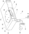
- Fig. 2 is a diagram of an example transition chill plate (TCP) 200 including wafer handler cleaning tool 100.
- Wafer handler cleaning tool 100 may be a device or a set of devices configured to remove foreign objects, debris, and/or other types of matter from an underside of a wafer handler included in a robotic arm.
- the robotic arm may be configured to transfer wafers between a wafer cassette and TCP 200.
- TCP 200 may include a housing 202, an upper surface 204, a front surface 206, and a chill plate 208.
- Chill plate 208 may be positioned on upper surface 204 and secured to upper surface 204 by fasteners 210 (e.g., screws, bolts, rivets, clips, and/or other types of fasteners).
- Chill plate 208 may be configured to cool a wafer positioned above chill plate 208 and placed on support pins 212.
- Mounting plate 104 of wafer handler cleaning tool 100 may be attached, connected, and/or otherwise secured to front surface 206 of TCP 200.
- Scraping device 102 may be positioned such that scraping edge 116 removes foreign objects, debris, and/or other types of matter removed from the underside of the wafer handler as the wafer handler passes through opening 118 in scraping device 102.
- scraping device 102 may be positioned such that the height of scraping edge 116 relative to the height of support pins 212 causes scraping edge 116 to remove foreign objects, debris, and/or other types of matter from the underside of the wafer handler as the wafer handler loads wafers onto support pins 212 and/or unloads wafers from support pins 212.
- TCP 200 may be utilized at the beginning or the end of a semiconductor processing flow for a wafer.
- TCP 200 may be a 2-5 TCP.
- a 2-5 TCP is a transition chill plate that is used to cool a wafer at the end of a semiconductor processing flow in which the wafer is processed through one or more semiconductor processing steps.
- the wafer may be transferred to the 2-5 TCP from a final processing stage (e.g., a 2-14 or a 2-24 high speed low temperature hot plate (HSL) or a 2-23 precision chilling hot plate process station (PCH) by a process robot), and a robotic arm may transfer the wafer from the 2-5 TCP to a wafer cassette.
- a final processing stage e.g., a 2-14 or a 2-24 high speed low temperature hot plate (HSL) or a 2-23 precision chilling hot plate process station (PCH) by a process robot
- HSL high speed low temperature hot plate
- PCH 2-23 precision chilling hot plate process station
- TCP 200 may be positioned below a 2-6 transition stage (TRS) unit, which is a transition stage unit in which wafers are placed prior to a semiconductor processing flow.
- TRS transition stage
- the robotic arm may transfer the wafers from a wafer cassette to the 2-6 TRS such that the wafers may be processed through the semiconductor processing flow. Accordingly, including wafer handler cleaning tool 100 in TCP 200 instead of the 2-6 TRS prevents wafer handler cleaning tool 100 from blocking the entrance or opening to the 2-6 TRS.
- TCP 200 e.g., a 2-5 TCP
- wafer handler cleaning tool 100 ensures that wafer handler cleaning tool 100 cleans the wafer handler during the transfer of each wafer from TCP 200 to a wafer cassette, which ensures that the wafer handler is cleaned more frequently relative to manual cleaning procedures.
- Fig. 2 The number and arrangement of components shown in Fig. 2 is provided as an example. In practice, the devices of Fig. 2 may include additional components, fewer components, different components, or differently arranged components than those shown in Fig. 2 .
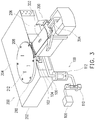
- Fig. 3 is a diagram of TCP 200, including wafer handler cleaning tool 100, and a robotic arm 300.
- Wafer handler cleaning tool 100 may be a device or set of devices configured to remove foreign objects, debris, and/or other types of matter from an underside of wafer handler 302 included in the robotic arm 300.
- the robotic arm 300 may be configured to transfer wafers between a wafer cassette and TCP 200.
- robotic arm 300 may further include a track 304 along which wafer handler 302 may travel.
- Track 304 permits wafer handler 302 to extend outward relative to robot arm 300 to load wafers into and unload wafers from TCP 200.
- wafer handler 302 may travel through opening 118 of wafer handler cleaning tool 100.
- scraping edge 116 may remove foreign objects, debris, and/or other types of matter from the underside of wafer handler 302. The removed foreign objects, debris, and/or other types of matter may be drawn through drain line 106 by negative pressure device 108, and may be collected, trapped, or caught by filtration device 112.
- Fig. 3 The number and arrangement of components shown in Fig. 3 is provided as an example. In practice, the devices of Fig. 3 may include additional components, fewer components, different components, or differently arranged components than those shown in Fig. 3 .
- Fig. 4 is a diagram of an example environment 400 in which systems and/or methods described herein may be implemented.
- environment 400 may include one or more wafer cassettes 402 configured into a wafer cassette block 404, a robotic arm 300 including a wafer handler 302 configured to hold a wafer 406, a wafer handler cleaning tool 100, and a TCP 200 or a semiconductor processing chamber 408.
- the tools and/or devices included in example environment 400 may be included in a semiconductor clean room, a semiconductor foundry, a semiconductor processing and/or manufacturing facility, and/or the like.
- Wafer cassette 402 may include a device configured to hold and/or store a plurality of wafers 406.
- wafer cassette 402 may include a plurality of slots. The plurality of slots may be vertically stacked in wafer cassette 402. Each of the plurality of slots may be configured to hold or store a wafer 406.
- Wafer cassette block 404 may include a row of a plurality of wafer cassettes 402. In some implementations, each wafer cassette 402 may hold or store a wafer lot. In some implementations, wafer cassette block 404 may hold or store a wafer lot across a plurality of wafer cassettes 402.
- robotic arm 300 may include a cassette block robotics arm (CRA) associated with wafer cassette block 404 and configured to transfer wafers 406 between TCP 200 and a wafer cassette 402.
- Robotic arm 300 may be capable of rotating wafer handler 302 180 degrees and/or 360 degrees to transfer wafers 406 between TCP 200 and a wafer cassette 402.
- robotic arm 300 may be capable of extending wafer handler 302 into TCP 200 to load a wafer 406 into TCP 200, to unload a wafer 406 from TCP 200, and/or the like.
- robotic arm 300 may be capable of extending wafer handler 302 into a wafer cassette 402 to load a wafer 406 into the wafer cassette 402, to unload a wafer 406 from the wafer cassette 402, and/or the like.
- robotic arm 300 may include a processing chamber loading arm associated with semiconductor processing chamber 408 and configured to transfer wafers 406 between semiconductor processing chamber 408 and a wafer cassette 402.
- Robotic arm 300 may be capable of rotating wafer handler 302 180 degrees and/or 360 degrees to transfer wafers 406 between semiconductor processing chamber 408 and a wafer cassette 402.
- robotic arm 300 may be capable of extending wafer handler 302 into semiconductor processing chamber 408 to load a wafer 406 into semiconductor processing chamber 408, to unload a wafer 406 from semiconductor processing chamber 408, and/or the like.
- robotic arm 300 may be capable of extending wafer handler 302 into a wafer cassette 402 to load a wafer 406 into the wafer cassette 402, to unload a wafer 406 from the wafer cassette 402, and/or the like.
- Semiconductor processing chamber 408 may include a processing chamber or tool configured to perform one or more semiconductor processing steps on a wafer 406.
- semiconductor processing chamber 408 may include a pre-clean chamber, a deposition chamber, an etching camber, a lithography chamber, or another type of semiconductor processing chamber.
- Wafer handler cleaning tool 100 may be located and/or positioned at and/or near an opening 410 of TCP 200 and/or semiconductor processing chamber 408. In this way, wafer handler cleaning tool 100 may clean an underside of wafer handler 302 as wafer handler 302 enters TCP 200 or semiconductor processing chamber 408 through opening 410 to load and/or unload a wafer 406. Wafer handler cleaning tool 100 may clean the underside of wafer handler 302 by removing foreign objects, debris, and/or other types of matter from the underside or bottom of wafer handler 302.
- the number and arrangement of devices and networks shown in Fig. 4 are provided as one or more examples. In practice, there may be additional devices, fewer devices, different devices, or differently arranged devices than those shown in Fig. 4 . Furthermore, two or more devices shown in Fig. 4 may be implemented within a single device, or a single device shown in Fig. 4 may be implemented as multiple, distributed devices. Additionally, or alternatively, a set of devices (e.g., one or more devices) of environment 400 may perform one or more functions described as being performed by another set of devices of environment 400.
- Figs. 5A-5D are diagrams illustrating example parameters for scraping device 102, wafer handler 302, and a slot of wafer cassette 402.
- an example parameter A may be a height of back wall 122.
- An example parameter B may be a height of front wall 120.
- An example parameter C may be a width of opening 118.
- An example parameter D may be a height of sidewalls 114 relative to the height of back wall 122.
- An example parameter E may be a top level of sidewalls 114.
- an example parameter F may be a thickness of wafer handler 302.
- An example parameter H may be a height or top level of a top side of wafer handler 302.
- An example parameter G may be a width of wafer handler 302.
- an example parameter I may be a gap size between the underside of wafer handler 302 and scraping edge 116.
- an example parameter J may be a gap size between the underside of wafer handler 302 and a top side of a wafer 406 in a slot of wafer cassette 402 below wafer handler 302.
- the height of back wall 122 may be greater than the height of front wall 120 (e.g., parameter A > parameter B) such that foreign objects, debris, and/or other types of matter removed from the underside of wafer handler 302 by scraping edge 116 falls into trough 126 as wafer handler 302 travels through opening 118.
- the width of opening 118 may be greater than the width of wafer handler 302 (e.g., parameter C > parameter G) such that wafer handler 302 is permitted to travel through opening 118.
- the height of sidewalls 114 may be greater than the thickness of wafer handler 302 (e.g., parameter D > parameter F) such that the top level of sidewalls 114 is greater than or higher than the top level of wafer handler 302 (e.g., parameter E > parameter H).
- the gap size between the underside of wafer handler 302 and scraping edge 116 may be less than the gap size between the underside of wafer handler 302 and the top side of the wafer 406 in the slot of wafer cassette 402 below wafer handler 302 (parameter I ⁇ parameter J).
- scraping edge 116 removes foreign objects, debris, and/or other types of matter from the underside of wafer handler 302 that are sized equal to or larger than the gap size between the underside of wafer handler 302 and the top side of the wafer 406, which prevents the foreign objects, debris, and/or other types of matter from causing damage to wafer 406.
- Figs. 5A-5D are provided as one or more examples. Other examples may differ from what is described with regard to Figs. 5A-5D .
- Fig. 6 is a diagram of example components of a device 600.
- wafer handler cleaning tool 100, TCP 200, wafer handler 302, robotic arm 300, and/or semiconductor processing chamber 408 may include one or more devices 600 and/or one or more components of device 600.
- device 600 may include a bus 610, a processor 620, a memory 630, a storage component 640, an input component 650, an output component 660, and a communication interface 670.
- Bus 610 includes a component that permits communication among multiple components of device 600.
- Processor 620 is implemented in hardware, firmware, and/or a combination of hardware and software.
- Processor 620 is a central processing unit (CPU), a graphics processing unit (GPU), an accelerated processing unit (APU), a microprocessor, a microcontroller, a digital signal processor (DSP), a field-programmable gate array (FPGA), an application-specific integrated circuit (ASIC), or another type of processing component.
- processor 620 includes one or more processors capable of being programmed to perform a function.
- Memory 630 includes a random access memory (RAM), a read only memory (ROM), and/or another type of dynamic or static storage device (e.g., a flash memory, a magnetic memory, and/or an optical memory) that stores information and/or instructions for use by processor 620.
- RAM random access memory
- ROM read only memory
- static storage device e.g., a flash memory, a magnetic memory, and/or an optical memory
- Storage component 640 stores information and/or software related to the operation and use of device 600.
- storage component 640 may include a hard disk (e.g., a magnetic disk, an optical disk, and/or a magneto-optic disk), a solid state drive (SSD), a compact disc (CD), a digital versatile disc (DVD), a floppy disk, a cartridge, a magnetic tape, and/or another type of non-transitory computer-readable medium, along with a corresponding drive.
- Input component 650 includes a component that permits device 600 to receive information, such as via user input (e.g., a touch screen display, a keyboard, a keypad, a mouse, a button, a switch, and/or a microphone). Additionally, or alternatively, input component 650 may include a component for determining location (e.g., a global positioning system (GPS) component) and/or a sensor (e.g., an accelerometer, a gyroscope, an actuator, another type of positional or environmental sensor, and/or the like).
- Output component 660 includes a component that provides output information from device 600 (via, e.g., a display, a speaker, a haptic feedback component, an audio or visual indicator, and/or the like).
- Communication interface 670 includes a transceiver-like component (e.g., a transceiver, a separate receiver, a separate transmitter, and/or the like) that enables device 600 to communicate with other devices, such as via a wired connection, a wireless connection, or a combination of wired and wireless connections.
- Communication interface 670 may permit device 600 to receive information from another device and/or provide information to another device.
- communication interface 670 may include an Ethernet interface, an optical interface, a coaxial interface, an infrared interface, a radio frequency (RF) interface, a universal serial bus (USB) interface, a Wi-Fi interface, a cellular network interface, and/or the like.
- RF radio frequency
- USB universal serial bus
- Device 600 may perform one or more processes described herein. Device 600 may perform these processes based on processor 620 executing software instructions stored by a non-transitory computer-readable medium, such as memory 630 and/or storage component 640.
- a non-transitory computer-readable medium such as memory 630 and/or storage component 640.
- computer-readable medium refers to a non-transitory memory device.
- a memory device includes memory space within a single physical storage device or memory space spread across multiple physical storage devices.
- Software instructions may be read into memory 630 and/or storage component 640 from another computer-readable medium or from another device via communication interface 670. When executed, software instructions stored in memory 630 and/or storage component 640 may cause processor 620 to perform one or more processes described herein. Additionally, or alternatively, hardware circuitry may be used in place of or in combination with software instructions to perform one or more processes described herein. Thus, implementations described herein are not limited to any specific combination of hardware circuitry and software.
- device 600 may include additional components, fewer components, different components, or differently arranged components than those shown in Fig. 6 . Additionally, or alternatively, a set of components (e.g., one or more components) of device 600 may perform one or more functions described as being performed by another set of components of device 600.
- a wafer handler cleaning tool includes a scraping device positioned near semiconductor equipment (e.g., a cooling plate, a semiconductor processing device, and/or the like) such that the scraping device removes foreign objects, debris, and/or other types of matter from the underside of the wafer handler when the wafer handler loads a wafer into the semiconductor equipment and/or unloads the wafer from the semiconductor equipment.
- the wafer handler cleaning tool may include a negative pressure device to draw the removed foreign objects, debris, and/or other types of matter away from the scraping device and toward a filtration device such that the filtration device captures the removed foreign objects, debris, and/or other types of matter.
- the wafer handler cleaning tool may clean the underside of the wafer handler prior to the wafer handler transferring a wafer to and/or from a wafer cassette. This reduces the likelihood of and/or prevents damage from occurring to another wafer that is loaded in a slot below the wafer in the wafer cassette. Moreover, the wafer handler cleaning tool may automatically clean the underside of the wafer handler, which reduces the downtime of the wafer handler that would otherwise result from manual cleaning of the wafer handler and allows for the wafer handler to be cleaned more frequently.
- the wafer handler cleaning tool includes a scraping device to remove debris from an underside of a robotic wafer handler.
- the wafer handler cleaning tool includes a negative pressure device to cause the debris, removed from the underside of the robotic wafer handler by the scraping device, to travel through a drain line.
- the wafer handler cleaning tool includes a filtration device to filter the debris from the drain line.
- the wafer handler cleaning tool includes a scraping device and a filtration device.
- the scraping device includes a scraping edge to remove foreign objects from of an underside of a robotic wafer handler as the robotic wafer handler loads a wafer to a chill plate or unloads the wafer from the chill plate.
- the scraping device includes a trough to collect the foreign objects removed from the underside of the robotic wafer handler.
- the scraping device includes a drain port to provide the foreign objects from the trough to a drain line.
- the filtration device is to filter the foreign objects from the drain line.
- the TCP includes a chill plate to cool a wafer after the wafer is processed through one or more semiconductor processing steps.
- the TCP includes a wafer handler cleaning tool.
- the wafer handler cleaning tool includes a mounting plate attached to a front side of TCP.
- the wafer handler cleaning tool includes a scraping device supported by the mounting plate and positioned to remove matter of at least a threshold size from an underside of a robotic wafer handler as the robotic wafer handler travels through an opening of the scraping device to unload the wafer from the chill plate.
Landscapes
- Container, Conveyance, Adherence, Positioning, Of Wafer (AREA)
- Cleaning Or Drying Semiconductors (AREA)
- Cleaning In General (AREA)
- Filtering Of Dispersed Particles In Gases (AREA)
Abstract
A wafer handler cleaning tool may include a scraping device positioned near semiconductor equipment (e.g., a cooling plate, a semiconductor processing device, and/or the like) such that the scraping device removes foreign objects, debris, and/or other types of matter from the underside of the wafer handler when the wafer handler loads a wafer into the semiconductor equipment and/or unloads the wafer from the semiconductor equipment. Moreover, the wafer handler cleaning tool may include a negative pressure device to draw the removed foreign objects, debris, and/or other types of matter away from the scraping device and toward a filtration device such that the filtration device captures the removed foreign objects, debris, and/or other types of matter.
Description
- A robotic arm is a device that is used to transfer wafers between various locations and/or processing equipment in a semiconductor processing facility.
- Aspects of the present disclosure are best understood from the following detailed description when read with the accompanying figures. It is noted that, in accordance with the standard practice in the industry, various features are not drawn to scale. In fact, the dimensions of the various features may be arbitrarily increased or reduced for clarity of discussion.
-
Figs. 1A and1B are diagrams of an example wafer handler cleaning tool described herein. -
Fig. 2 is a diagram of an example transition chill plate including the wafer handler cleaning tool ofFigs. 1A and1B . -
Fig. 3 is a diagram of an example transition chill plate, including the wafer handler cleaning tool ofFigs. 1A and1B , and a wafer handler. -
Fig. 4 is a diagram of an example environment in which systems and/or methods described herein may be implemented. -
Figs. 5A-5D are diagrams illustrating example parameters for a scraping device, a wafer handler, and a wafer cassette slot. -
Fig. 6 is a diagram of example components of one or more devices described herein. - The following disclosure provides many different embodiments, or examples, for implementing different features of the provided subject matter. Specific examples of components and arrangements are described below to simplify the present disclosure. These are, of course, merely examples and are not intended to be limiting. For example, the formation of a first feature over or on a second feature in the description that follows may include embodiments in which the first and second features are formed in direct contact, and may also include embodiments in which additional features may be formed between the first and second features, such that the first and second features may not be in direct contact. In addition, the present disclosure may repeat reference numerals and/or letters in the various examples. This repetition is for the purpose of simplicity and clarity and does not in itself dictate a relationship between the various embodiments and/or configurations discussed.
- Further, spatially relative terms, such as "beneath," "below," "lower," "above," "upper" and the like, may be used herein for ease of description to describe one element or feature's relationship to another element(s) or feature(s) as illustrated in the figures. The spatially relative terms are intended to encompass different orientations of the device in use or operation in addition to the orientation depicted in the figures. The apparatus may be otherwise oriented (rotated 90 degrees or at other orientations) and the spatially relative descriptors used herein may likewise be interpreted accordingly.
- In some cases, a robotic arm may transfer a wafer between a wafer cassette (e.g., a container that is configured to store a plurality of wafers) and a semiconductor processing chamber or chill plate. The wafer cassette may include a plurality of slots, where each slot is configured to store a wafer. Wafers may be placed in the wafer cassette before and/or after processing.
- The robotic arm may include a wafer handler or pincette that is configured and/or shaped to hold a wafer. In some cases, foreign objects (e.g., plastic fibers from device packaging, dust particles, and/or other types of foreign objects), debris, and/or other types of matter may cling to the underside (or bottom) of the wafer handler (e.g., due to an electrostatic charge). These foreign objects, debris, and/or other types of matter on the underside of the wafer handler can cause physical damage (e.g., a scratch and/or the like) to a wafer when the wafer handler loads or unloads another wafer in a slot above the wafer in a wafer cassette. This physical damage may result in rework and/or repairs to the wafer, may result in the wafer being scrapped, and/or the like.
- Some implementations described herein provide a wafer handler cleaning tool that is capable of removing foreign objects, debris, and/or other types of matter from the underside of a wafer handler of a robotic arm. The wafer handler cleaning tool includes a scraping device positioned near semiconductor equipment (e.g., a cooling plate, a semiconductor processing device, and/or the like) such that the scraping device removes foreign objects, debris, and/or other types of matter from the underside of the wafer handler when the wafer handler loads a wafer into the semiconductor equipment and/or unloads the wafer from the semiconductor equipment. Moreover, the wafer handler cleaning tool may include a negative pressure device to draw the removed foreign objects, debris, and/or other types of matter away from the scraping device and toward a filtration device such that the filtration device captures the removed foreign objects, debris, and/or other types of matter.
- In this way, the wafer handler cleaning tool may clean the underside of the wafer handler prior to the wafer handler transferring a wafer to and/or from a wafer cassette. This reduces the likelihood of and/or prevents damage from occurring to another wafer that is loaded in a slot below the wafer in the wafer cassette. Moreover, the wafer handler cleaning tool may automatically clean the underside of the wafer handler, which reduces the downtime of the wafer handler that would otherwise result from manual cleaning of the wafer handler and allows for the wafer handler to be cleaned more frequently.
-
Figs. 1A and1B are diagrams of an example waferhandler cleaning tool 100 described herein. Waferhandler cleaning tool 100 may be a device or a set of devices configured to remove foreign objects, debris, and/or other types of matter from an underside of a wafer handler included in a robotic arm. The robotic arm may be configured to transfer wafers between a wafer cassette and semiconductor processing equipment, such as a semiconductor processing chamber, a transition chill plate (TCP), and/or the like. - As shown in
Fig. 1A , waferhandler cleaning tool 100 may include various components, such as ascraping device 102, amounting plate 104, adrain line 106, anegative pressure device 108, aflow meter 110, and afiltration device 112. Scrapingdevice 102 may be a component configured to remove foreign objects, debris, and/or other types of matter from the underside of the wafer handler. Scrapingdevice 102 may be formed of one or more materials, such as a metal, a plastic, a rubber, a composite, another material, and/or a combination thereof. Scrapingdevice 102 may be attached to, connected to, or integrated withmounting plate 104.Mounting plate 104 may attach, connect, mount, and/or otherwise securescraping device 102 to a semiconductor processing equipment.Mounting plate 104 may attach to a front side of the semiconductor processing equipment at or near an opening of the semiconductor processing equipment.Mounting plate 104 may be formed of one or more materials, such as a metal, a plastic, a composite, another material, and/or a combination thereof. - The foreign objects, debris, and/or other types of matter removed from the underside of the wafer handler by
scraping device 102 may be provided to drainline 106.Drain line 106 may connect to scrapingdevice 102 and may collect the foreign objects, debris, and/or other types of matter removed from the underside of the wafer handler.Drain line 106 may be a flexible or rigid pipe, tube, and/or a combination thereof. The inside diameter ofdrain line 106 may be sized according to the expected sizes of the foreign objects, debris, and/or other types of matter to be removed from the underside of the wafer handler. -
Negative pressure device 108 may include a pump, a fan, a motor, or another type of device capable of generating a negative pressure indrain line 106. The negative pressure indrain line 106 draws the removed foreign objects, debris, and/or other types of matter away fromscraping device 102 and intodrain line 106.Flow meter 110 may be a mass flow meter, an electromagnetic flow meter, or another type of flow meter that is capable of measuring a flow rate of air throughdrain line 106. Moreover,flow meter 110 may provide an indication of the flow rate throughdrain line 106 such that the flow rate can be observed to determine whether waferhandler cleaning tool 100 is operating within acceptable operating parameters. -
Filtration device 112 may include various types of air filters, such as a paper filter, a metal mesh filter, and/or the like.Filtration device 112 may be positioned between and connected to two portions or sections ofdrain line 106 such that air drawn throughdrain line 106 bynegative pressure device 108 passes throughfiltration device 112. In this way, foreign objects, debris, and/or other types of matter drawn throughdrain line 106 by the negative pressure generated bynegative pressure device 108 are trapped or captured byfiltration device 112. Moreover,filtration device 112 may be positioned alongdrain line 106 prior toflow meter 110 such thatfiltration device 112 filters foreign objects, debris, and/or other types of matter before the foreign objects, debris, and/or other types of matter reachesflow meter 110 and causes a blockage atflow meter 110.Filtration device 112 may include a canister or another type of housing in which a filter is inserted. The housing may be opened to remove the filter for cleaning or replacement, such as in situations whereflow meter 110 indicates that the negative pressure indrain line 106 does not satisfy a negative pressure threshold. - As shown in
Fig. 1B ,scraping device 102 may include a pair ofsidewalls 114 and ascraping edge 116.Sidewalls 114 may be formed on opposing sides of scrapingedge 116.Sidewalls 114 may be formed to a raised height relative to the height of scrapingedge 116 to form anopening 118 through which the wafer handler may travel. The height of scrapingedge 116 may be configured such that scrapingedge 116 removes foreign objects, debris, and/or other types of matter from the underside (or bottom) of the wafer handler when the wafer handler travels throughopening 118. - In some implementations, scraping
edge 116 may remove or scrape foreign objects, debris, and/or other types of matter from the underside of the wafer handler that are sized equal to or greater than a gap size between scrapingedge 116 and the underside of the wafer handler. In these examples, scrapingedge 116 does not physically touch the wafer handler. In some implementations, scrapingedge 116 may remove or scrape foreign objects, debris, and/or other types of matter from the underside of the wafer handler by physically contacting (e.g., scraping or rubbing against) the underside of the wafer handler. - As further shown in
Fig. 1B ,scraping device 102 may include afront wall 120, aback wall 122, and a plurality ofsidewalls 124.Sidewalls 114 and scrapingedge 116 may be part ofback wall 122.Front wall 120,back wall 122, and sidewalls 124 may form atrough 126.Trough 126 may be sized and configured to collect foreign objects, debris, and/or other types of matter removed from the underside of the wafer handler. The foreign objects, debris, and/or other types of matter removed from the underside of the wafer handler may be drawn intotrough 126 by gravity and/or the negative pressure generated bynegative pressure device 108. The foreign objects, debris, and/or other types of matter removed from the underside of the wafer handler may collect at the bottom oftrough 126 and may be drawn through adrain port 128 at the bottom oftrough 126.Drain port 128 may connect to drainline 106. - The number and arrangement of components shown in
Figs. 1A and1B are provided as an example. In practice, waferhandler cleaning tool 100 may include additional components, fewer components, different components, or differently arranged components than those shown inFigs. 1A and1B . -
Fig. 2 is a diagram of an example transition chill plate (TCP) 200 including waferhandler cleaning tool 100. Waferhandler cleaning tool 100 may be a device or a set of devices configured to remove foreign objects, debris, and/or other types of matter from an underside of a wafer handler included in a robotic arm. The robotic arm may be configured to transfer wafers between a wafer cassette andTCP 200. - As shown in
Fig. 2 ,TCP 200 may include ahousing 202, anupper surface 204, afront surface 206, and achill plate 208.Chill plate 208 may be positioned onupper surface 204 and secured toupper surface 204 by fasteners 210 (e.g., screws, bolts, rivets, clips, and/or other types of fasteners).Chill plate 208 may be configured to cool a wafer positioned abovechill plate 208 and placed on support pins 212. Mountingplate 104 of waferhandler cleaning tool 100 may be attached, connected, and/or otherwise secured tofront surface 206 ofTCP 200. -
Scraping device 102 may be positioned such that scrapingedge 116 removes foreign objects, debris, and/or other types of matter removed from the underside of the wafer handler as the wafer handler passes throughopening 118 in scrapingdevice 102. In particular, scrapingdevice 102 may be positioned such that the height of scrapingedge 116 relative to the height of support pins 212causes scraping edge 116 to remove foreign objects, debris, and/or other types of matter from the underside of the wafer handler as the wafer handler loads wafers onto support pins 212 and/or unloads wafers from support pins 212. - In some implementations,
TCP 200 may be utilized at the beginning or the end of a semiconductor processing flow for a wafer. For example,TCP 200 may be a 2-5 TCP. A 2-5 TCP is a transition chill plate that is used to cool a wafer at the end of a semiconductor processing flow in which the wafer is processed through one or more semiconductor processing steps. The wafer may be transferred to the 2-5 TCP from a final processing stage (e.g., a 2-14 or a 2-24 high speed low temperature hot plate (HSL) or a 2-23 precision chilling hot plate process station (PCH) by a process robot), and a robotic arm may transfer the wafer from the 2-5 TCP to a wafer cassette. In these examples,TCP 200 may be positioned below a 2-6 transition stage (TRS) unit, which is a transition stage unit in which wafers are placed prior to a semiconductor processing flow. The robotic arm may transfer the wafers from a wafer cassette to the 2-6 TRS such that the wafers may be processed through the semiconductor processing flow. Accordingly, including waferhandler cleaning tool 100 inTCP 200 instead of the 2-6 TRS prevents waferhandler cleaning tool 100 from blocking the entrance or opening to the 2-6 TRS. Moreover, including waferhandler cleaning tool 100 in TCP 200 (e.g., a 2-5 TCP) ensures that waferhandler cleaning tool 100 cleans the wafer handler during the transfer of each wafer fromTCP 200 to a wafer cassette, which ensures that the wafer handler is cleaned more frequently relative to manual cleaning procedures. - The number and arrangement of components shown in
Fig. 2 is provided as an example. In practice, the devices ofFig. 2 may include additional components, fewer components, different components, or differently arranged components than those shown inFig. 2 . -
Fig. 3 is a diagram ofTCP 200, including waferhandler cleaning tool 100, and arobotic arm 300. Waferhandler cleaning tool 100 may be a device or set of devices configured to remove foreign objects, debris, and/or other types of matter from an underside ofwafer handler 302 included in therobotic arm 300. Therobotic arm 300 may be configured to transfer wafers between a wafer cassette andTCP 200. - As shown in
Fig. 3 ,robotic arm 300 may further include atrack 304 along whichwafer handler 302 may travel. Track 304 permitswafer handler 302 to extend outward relative torobot arm 300 to load wafers into and unload wafers fromTCP 200. As further shown inFig. 3 , aswafer handler 302 travels alongtrack 304 to extend outward and intoTCP 200,wafer handler 302 may travel through opening 118 of waferhandler cleaning tool 100. Aswafer handler 302 travels throughopening 118, scrapingedge 116 may remove foreign objects, debris, and/or other types of matter from the underside ofwafer handler 302. The removed foreign objects, debris, and/or other types of matter may be drawn throughdrain line 106 bynegative pressure device 108, and may be collected, trapped, or caught byfiltration device 112. - The number and arrangement of components shown in
Fig. 3 is provided as an example. In practice, the devices ofFig. 3 may include additional components, fewer components, different components, or differently arranged components than those shown inFig. 3 . -
Fig. 4 is a diagram of anexample environment 400 in which systems and/or methods described herein may be implemented. As shown inFig. 4 ,environment 400 may include one ormore wafer cassettes 402 configured into awafer cassette block 404, arobotic arm 300 including awafer handler 302 configured to hold awafer 406, a waferhandler cleaning tool 100, and aTCP 200 or asemiconductor processing chamber 408. The tools and/or devices included inexample environment 400 may be included in a semiconductor clean room, a semiconductor foundry, a semiconductor processing and/or manufacturing facility, and/or the like. -
Wafer cassette 402 may include a device configured to hold and/or store a plurality ofwafers 406. For example,wafer cassette 402 may include a plurality of slots. The plurality of slots may be vertically stacked inwafer cassette 402. Each of the plurality of slots may be configured to hold or store awafer 406.Wafer cassette block 404 may include a row of a plurality ofwafer cassettes 402. In some implementations, eachwafer cassette 402 may hold or store a wafer lot. In some implementations,wafer cassette block 404 may hold or store a wafer lot across a plurality ofwafer cassettes 402. - In some implementations,
robotic arm 300 may include a cassette block robotics arm (CRA) associated withwafer cassette block 404 and configured to transferwafers 406 betweenTCP 200 and awafer cassette 402.Robotic arm 300 may be capable of rotatingwafer handler 302 180 degrees and/or 360 degrees to transferwafers 406 betweenTCP 200 and awafer cassette 402. For example,robotic arm 300 may be capable of extendingwafer handler 302 intoTCP 200 to load awafer 406 intoTCP 200, to unload awafer 406 fromTCP 200, and/or the like. As another example,robotic arm 300 may be capable of extendingwafer handler 302 into awafer cassette 402 to load awafer 406 into thewafer cassette 402, to unload awafer 406 from thewafer cassette 402, and/or the like. - In some implementations,
robotic arm 300 may include a processing chamber loading arm associated withsemiconductor processing chamber 408 and configured to transferwafers 406 betweensemiconductor processing chamber 408 and awafer cassette 402.Robotic arm 300 may be capable of rotatingwafer handler 302 180 degrees and/or 360 degrees to transferwafers 406 betweensemiconductor processing chamber 408 and awafer cassette 402. For example,robotic arm 300 may be capable of extendingwafer handler 302 intosemiconductor processing chamber 408 to load awafer 406 intosemiconductor processing chamber 408, to unload awafer 406 fromsemiconductor processing chamber 408, and/or the like. As another example,robotic arm 300 may be capable of extendingwafer handler 302 into awafer cassette 402 to load awafer 406 into thewafer cassette 402, to unload awafer 406 from thewafer cassette 402, and/or the like. -
Semiconductor processing chamber 408 may include a processing chamber or tool configured to perform one or more semiconductor processing steps on awafer 406. For example,semiconductor processing chamber 408 may include a pre-clean chamber, a deposition chamber, an etching camber, a lithography chamber, or another type of semiconductor processing chamber. - Wafer
handler cleaning tool 100 may be located and/or positioned at and/or near anopening 410 ofTCP 200 and/orsemiconductor processing chamber 408. In this way, waferhandler cleaning tool 100 may clean an underside ofwafer handler 302 aswafer handler 302 entersTCP 200 orsemiconductor processing chamber 408 throughopening 410 to load and/or unload awafer 406. Waferhandler cleaning tool 100 may clean the underside ofwafer handler 302 by removing foreign objects, debris, and/or other types of matter from the underside or bottom ofwafer handler 302. - The number and arrangement of devices and networks shown in
Fig. 4 are provided as one or more examples. In practice, there may be additional devices, fewer devices, different devices, or differently arranged devices than those shown inFig. 4 . Furthermore, two or more devices shown inFig. 4 may be implemented within a single device, or a single device shown inFig. 4 may be implemented as multiple, distributed devices. Additionally, or alternatively, a set of devices (e.g., one or more devices) ofenvironment 400 may perform one or more functions described as being performed by another set of devices ofenvironment 400. -
Figs. 5A-5D are diagrams illustrating example parameters for scrapingdevice 102,wafer handler 302, and a slot ofwafer cassette 402. As shown inFig. 5A , an example parameter A may be a height ofback wall 122. An example parameter B may be a height offront wall 120. An example parameter C may be a width ofopening 118. An example parameter D may be a height ofsidewalls 114 relative to the height ofback wall 122. An example parameter E may be a top level ofsidewalls 114. - As shown in
Fig. 5B , an example parameter F may be a thickness ofwafer handler 302. An example parameter H may be a height or top level of a top side ofwafer handler 302. An example parameter G may be a width ofwafer handler 302. As shown inFig. 5C , an example parameter I may be a gap size between the underside ofwafer handler 302 and scrapingedge 116. As shown inFig. 5D , an example parameter J may be a gap size between the underside ofwafer handler 302 and a top side of awafer 406 in a slot ofwafer cassette 402 belowwafer handler 302. - The height of
back wall 122 may be greater than the height of front wall 120 (e.g., parameter A > parameter B) such that foreign objects, debris, and/or other types of matter removed from the underside ofwafer handler 302 by scrapingedge 116 falls intotrough 126 aswafer handler 302 travels throughopening 118. The width ofopening 118 may be greater than the width of wafer handler 302 (e.g., parameter C > parameter G) such thatwafer handler 302 is permitted to travel throughopening 118. The height ofsidewalls 114 may be greater than the thickness of wafer handler 302 (e.g., parameter D > parameter F) such that the top level ofsidewalls 114 is greater than or higher than the top level of wafer handler 302 (e.g., parameter E > parameter H). The gap size between the underside ofwafer handler 302 and scrapingedge 116 may be less than the gap size between the underside ofwafer handler 302 and the top side of thewafer 406 in the slot ofwafer cassette 402 below wafer handler 302 (parameter I < parameter J). In this way, scrapingedge 116 removes foreign objects, debris, and/or other types of matter from the underside ofwafer handler 302 that are sized equal to or larger than the gap size between the underside ofwafer handler 302 and the top side of thewafer 406, which prevents the foreign objects, debris, and/or other types of matter from causing damage towafer 406. - As indicated above,
Figs. 5A-5D are provided as one or more examples. Other examples may differ from what is described with regard toFigs. 5A-5D . -
Fig. 6 is a diagram of example components of adevice 600. In some implementations, waferhandler cleaning tool 100,TCP 200,wafer handler 302,robotic arm 300, and/orsemiconductor processing chamber 408 may include one ormore devices 600 and/or one or more components ofdevice 600. As shown inFig. 6 ,device 600 may include a bus 610, aprocessor 620, amemory 630, astorage component 640, aninput component 650, anoutput component 660, and acommunication interface 670. - Bus 610 includes a component that permits communication among multiple components of
device 600.Processor 620 is implemented in hardware, firmware, and/or a combination of hardware and software.Processor 620 is a central processing unit (CPU), a graphics processing unit (GPU), an accelerated processing unit (APU), a microprocessor, a microcontroller, a digital signal processor (DSP), a field-programmable gate array (FPGA), an application-specific integrated circuit (ASIC), or another type of processing component. In some implementations,processor 620 includes one or more processors capable of being programmed to perform a function.Memory 630 includes a random access memory (RAM), a read only memory (ROM), and/or another type of dynamic or static storage device (e.g., a flash memory, a magnetic memory, and/or an optical memory) that stores information and/or instructions for use byprocessor 620. -
Storage component 640 stores information and/or software related to the operation and use ofdevice 600. For example,storage component 640 may include a hard disk (e.g., a magnetic disk, an optical disk, and/or a magneto-optic disk), a solid state drive (SSD), a compact disc (CD), a digital versatile disc (DVD), a floppy disk, a cartridge, a magnetic tape, and/or another type of non-transitory computer-readable medium, along with a corresponding drive. -
Input component 650 includes a component that permitsdevice 600 to receive information, such as via user input (e.g., a touch screen display, a keyboard, a keypad, a mouse, a button, a switch, and/or a microphone). Additionally, or alternatively,input component 650 may include a component for determining location (e.g., a global positioning system (GPS) component) and/or a sensor (e.g., an accelerometer, a gyroscope, an actuator, another type of positional or environmental sensor, and/or the like).Output component 660 includes a component that provides output information from device 600 (via, e.g., a display, a speaker, a haptic feedback component, an audio or visual indicator, and/or the like). -
Communication interface 670 includes a transceiver-like component (e.g., a transceiver, a separate receiver, a separate transmitter, and/or the like) that enablesdevice 600 to communicate with other devices, such as via a wired connection, a wireless connection, or a combination of wired and wireless connections.Communication interface 670 may permitdevice 600 to receive information from another device and/or provide information to another device. For example,communication interface 670 may include an Ethernet interface, an optical interface, a coaxial interface, an infrared interface, a radio frequency (RF) interface, a universal serial bus (USB) interface, a Wi-Fi interface, a cellular network interface, and/or the like. -
Device 600 may perform one or more processes described herein.Device 600 may perform these processes based onprocessor 620 executing software instructions stored by a non-transitory computer-readable medium, such asmemory 630 and/orstorage component 640. As used herein, the term "computer-readable medium" refers to a non-transitory memory device. A memory device includes memory space within a single physical storage device or memory space spread across multiple physical storage devices. - Software instructions may be read into
memory 630 and/orstorage component 640 from another computer-readable medium or from another device viacommunication interface 670. When executed, software instructions stored inmemory 630 and/orstorage component 640 may causeprocessor 620 to perform one or more processes described herein. Additionally, or alternatively, hardware circuitry may be used in place of or in combination with software instructions to perform one or more processes described herein. Thus, implementations described herein are not limited to any specific combination of hardware circuitry and software. - The number and arrangement of components shown in
Fig. 6 are provided as an example. In practice,device 600 may include additional components, fewer components, different components, or differently arranged components than those shown inFig. 6 . Additionally, or alternatively, a set of components (e.g., one or more components) ofdevice 600 may perform one or more functions described as being performed by another set of components ofdevice 600. - In this way, a wafer handler cleaning tool includes a scraping device positioned near semiconductor equipment (e.g., a cooling plate, a semiconductor processing device, and/or the like) such that the scraping device removes foreign objects, debris, and/or other types of matter from the underside of the wafer handler when the wafer handler loads a wafer into the semiconductor equipment and/or unloads the wafer from the semiconductor equipment. Moreover, the wafer handler cleaning tool may include a negative pressure device to draw the removed foreign objects, debris, and/or other types of matter away from the scraping device and toward a filtration device such that the filtration device captures the removed foreign objects, debris, and/or other types of matter. Thus, the wafer handler cleaning tool may clean the underside of the wafer handler prior to the wafer handler transferring a wafer to and/or from a wafer cassette. This reduces the likelihood of and/or prevents damage from occurring to another wafer that is loaded in a slot below the wafer in the wafer cassette. Moreover, the wafer handler cleaning tool may automatically clean the underside of the wafer handler, which reduces the downtime of the wafer handler that would otherwise result from manual cleaning of the wafer handler and allows for the wafer handler to be cleaned more frequently.
- As described in greater detail above, some implementations described herein provide a wafer handler cleaning tool. The wafer handler cleaning tool includes a scraping device to remove debris from an underside of a robotic wafer handler. The wafer handler cleaning tool includes a negative pressure device to cause the debris, removed from the underside of the robotic wafer handler by the scraping device, to travel through a drain line. The wafer handler cleaning tool includes a filtration device to filter the debris from the drain line.
- As described in greater detail above, some implementations described herein provide a wafer handler cleaning tool. The wafer handler cleaning tool includes a scraping device and a filtration device. The scraping device includes a scraping edge to remove foreign objects from of an underside of a robotic wafer handler as the robotic wafer handler loads a wafer to a chill plate or unloads the wafer from the chill plate. The scraping device includes a trough to collect the foreign objects removed from the underside of the robotic wafer handler. The scraping device includes a drain port to provide the foreign objects from the trough to a drain line. The filtration device is to filter the foreign objects from the drain line.
- As described in greater detail above, some implementations described herein provide a transition chill plate (TCP). The TCP includes a chill plate to cool a wafer after the wafer is processed through one or more semiconductor processing steps. The TCP includes a wafer handler cleaning tool. The wafer handler cleaning tool includes a mounting plate attached to a front side of TCP. The wafer handler cleaning tool includes a scraping device supported by the mounting plate and positioned to remove matter of at least a threshold size from an underside of a robotic wafer handler as the robotic wafer handler travels through an opening of the scraping device to unload the wafer from the chill plate.
- The foregoing outlines features of several embodiments so that those skilled in the art may better understand the aspects of the present disclosure. Those skilled in the art should appreciate that they may readily use the present disclosure as a basis for designing or modifying other processes and structures for carrying out the same purposes and/or achieving the same advantages of the embodiments introduced herein. Those skilled in the art should also realize that such equivalent constructions do not depart from the spirit and scope of the present disclosure, and that they may make various changes, substitutions, and alterations herein without departing from the spirit and scope of the present disclosure.
Claims (5)
- A wafer handler cleaning tool (100), comprising:a scraping device (102) to remove debris from an underside of a robotic wafer handler (302);a negative pressure device (108) to cause the debris, removed from the underside of the robotic wafer handler by the scraping device, to travel through a drain line (106); anda filtration device (112) to filter the debris from the drain line.
- The wafer handler cleaning tool of claim 1, further comprising:
a flow meter to provide an indication of a flow rate through the drain line. - The wafer handler cleaning tool of claim 2, wherein the filtration device is to filter the debris to prevent the debris from causing a blockage at the flow meter.
- The wafer handler cleaning tool of claim 1, wherein the wafer handler cleaning tool is positioned between a transition chill plate and a cassette block robotics arm (CRA) in which the robotic wafer handler is included; and
wherein the scraping device is to remove the debris from the underside of the robotic wafer handler as the CRA loads a wafer onto a chill plate or unloads the wafer from the chill plate. - The wafer handler cleaning tool of claim 1, wherein the wafer handler cleaning tool is positioned between a semiconductor processing chamber and a processing chamber loading arm in which the robotic wafer handler is included; and
wherein the scraping device is to remove the debris from the underside of the robotic wafer handler as the processing chamber loading arm loads a wafer into the semiconductor processing chamber or unloads the wafer from the semiconductor processing chamber.
Applications Claiming Priority (1)
| Application Number | Priority Date | Filing Date | Title |
|---|---|---|---|
| US16/946,890 US11666951B2 (en) | 2020-07-10 | 2020-07-10 | Wafer handler cleaning tool |
Publications (1)
| Publication Number | Publication Date |
|---|---|
| EP3937218A1 true EP3937218A1 (en) | 2022-01-12 |
Family
ID=76859490
Family Applications (1)
| Application Number | Title | Priority Date | Filing Date |
|---|---|---|---|
| EP21184759.5A Withdrawn EP3937218A1 (en) | 2020-07-10 | 2021-07-09 | Wafer handler cleaning tool |
Country Status (5)
| Country | Link |
|---|---|
| US (1) | US11666951B2 (en) |
| EP (1) | EP3937218A1 (en) |
| JP (1) | JP2022016410A (en) |
| CN (1) | CN113369181A (en) |
| TW (1) | TW202202243A (en) |
Families Citing this family (2)
| Publication number | Priority date | Publication date | Assignee | Title |
|---|---|---|---|---|
| US20220403506A1 (en) * | 2020-01-07 | 2022-12-22 | Lam Research Corporation | Automated cleaning of robot arms of substrate processing systems |
| JP2024013455A (en) * | 2022-07-20 | 2024-02-01 | 株式会社Screenホールディングス | Substrate processing equipment |
Citations (5)
| Publication number | Priority date | Publication date | Assignee | Title |
|---|---|---|---|---|
| JPH07254583A (en) * | 1994-03-16 | 1995-10-03 | Hitachi Ltd | Cleaning method and cleaning device |
| US6129100A (en) * | 1998-01-13 | 2000-10-10 | Hoya Corporation | Wafer cleaning apparatus and structure for holding and transferring wafer used in wafer cleaning apparatus |
| JP2002367945A (en) * | 2001-06-08 | 2002-12-20 | Rix Corp | Wafer cleaning system with wafer transfer robot |
| KR20060108086A (en) * | 2005-04-12 | 2006-10-17 | 삼성전자주식회사 | Wafer Handler Robot Arm |
| US20090255362A1 (en) * | 2008-04-15 | 2009-10-15 | Dynamic Micro Systems, Semiconductor Equipment Gmbh | Clean transfer robot |
Family Cites Families (5)
| Publication number | Priority date | Publication date | Assignee | Title |
|---|---|---|---|---|
| KR101103561B1 (en) * | 2009-07-13 | 2012-01-06 | 로체 시스템즈(주) | Finger cleaning method of wafer transfer robot and cleaner module for same |
| US20120211029A1 (en) * | 2011-02-22 | 2012-08-23 | Pandit Viraj S | Load lock assembly and method for particle reduction |
| JP2012199327A (en) * | 2011-03-18 | 2012-10-18 | Dainippon Screen Mfg Co Ltd | Substrate processing apparatus |
| JP5603314B2 (en) * | 2011-12-01 | 2014-10-08 | 東京エレクトロン株式会社 | Conveying apparatus and substrate processing system |
| US10861692B2 (en) * | 2017-10-26 | 2020-12-08 | Taiwan Semiconductor Manufacturing Co., Ltd. | Substrate carrier deterioration detection and repair |
-
2020
- 2020-07-10 US US16/946,890 patent/US11666951B2/en active Active
- 2020-11-05 CN CN202011221198.8A patent/CN113369181A/en active Pending
- 2020-11-05 TW TW109138523A patent/TW202202243A/en unknown
-
2021
- 2021-07-09 EP EP21184759.5A patent/EP3937218A1/en not_active Withdrawn
- 2021-07-09 JP JP2021113988A patent/JP2022016410A/en active Pending
Patent Citations (5)
| Publication number | Priority date | Publication date | Assignee | Title |
|---|---|---|---|---|
| JPH07254583A (en) * | 1994-03-16 | 1995-10-03 | Hitachi Ltd | Cleaning method and cleaning device |
| US6129100A (en) * | 1998-01-13 | 2000-10-10 | Hoya Corporation | Wafer cleaning apparatus and structure for holding and transferring wafer used in wafer cleaning apparatus |
| JP2002367945A (en) * | 2001-06-08 | 2002-12-20 | Rix Corp | Wafer cleaning system with wafer transfer robot |
| KR20060108086A (en) * | 2005-04-12 | 2006-10-17 | 삼성전자주식회사 | Wafer Handler Robot Arm |
| US20090255362A1 (en) * | 2008-04-15 | 2009-10-15 | Dynamic Micro Systems, Semiconductor Equipment Gmbh | Clean transfer robot |
Also Published As
| Publication number | Publication date |
|---|---|
| TW202202243A (en) | 2022-01-16 |
| US11666951B2 (en) | 2023-06-06 |
| JP2022016410A (en) | 2022-01-21 |
| US20220008966A1 (en) | 2022-01-13 |
| CN113369181A (en) | 2021-09-10 |
Similar Documents
| Publication | Publication Date | Title |
|---|---|---|
| US11666951B2 (en) | Wafer handler cleaning tool | |
| US10930536B2 (en) | Workpiece stocker with circular configuration | |
| US12237196B2 (en) | Docking device with moveable frame and sealing component | |
| CN109712867B (en) | Substrate carrier degradation detection and repair | |
| TWI864167B (en) | Multiple semiconductor die container load port | |
| US10474139B2 (en) | Substrate processing apparatus and substrate processing method | |
| US9766543B2 (en) | Liquid treatment method, substrate processing apparatus and non-transitory storage medium | |
| US20160020122A1 (en) | Substrate processing apparatus and substrate processing method | |
| JP3237741B2 (en) | Inspection equipment with high cleanliness | |
| US20230062038A1 (en) | Vent port diffuser | |
| US12217991B2 (en) | Portable robotic semiconductor pod loader | |
| US20240379391A1 (en) | Airflow detection device and methods of use | |
| JPH09153531A (en) | Highly clean inspection device | |
| JP6462444B2 (en) | Wafer transfer device | |
| CN117936439A (en) | Wafer cleaning device and cleaning method suitable for front-end module of semiconductor equipment | |
| US12272573B2 (en) | Load port and methods of operation | |
| JP6929105B2 (en) | Substrate processing equipment and substrate processing method | |
| KR20040040106A (en) | Apparatus removing static electricity of semiconductor wafer | |
| KR101246052B1 (en) | Blowing system for removal of dust particles on image sensor | |
| CN201773827U (en) | Automatic buffer system | |
| JPS63128621A (en) | Semiconductor manufacturing apparatus |
Legal Events
| Date | Code | Title | Description |
|---|---|---|---|
| PUAI | Public reference made under article 153(3) epc to a published international application that has entered the european phase |
Free format text: ORIGINAL CODE: 0009012 |
|
| STAA | Information on the status of an ep patent application or granted ep patent |
Free format text: STATUS: THE APPLICATION HAS BEEN PUBLISHED |
|
| AK | Designated contracting states |
Kind code of ref document: A1 Designated state(s): AL AT BE BG CH CY CZ DE DK EE ES FI FR GB GR HR HU IE IS IT LI LT LU LV MC MK MT NL NO PL PT RO RS SE SI SK SM TR |
|
| B565 | Issuance of search results under rule 164(2) epc |
Effective date: 20211206 |
|
| STAA | Information on the status of an ep patent application or granted ep patent |
Free format text: STATUS: THE APPLICATION IS DEEMED TO BE WITHDRAWN |
|
| 18D | Application deemed to be withdrawn |
Effective date: 20220713 |