Technical field of the invention
-
The present invention relates to the field of capturing fluorescence light in the time domain and determining its lifetime.
Background of the invention
-
A popular method to achieve fluorescence lifetime imaging is in the frequency domain. Light stimulating a fluorophore is modulated sinusoidally, and the received fluorescence light is demodulated with the same frequency, whereby phase change and modulation depth are the prime parameters to extract the lifetime of the fluorophore.
-
Another way is to use the principle of rapid lifetime determination. One measures the light response by collecting the number of photons in two time windows (or bins), with a very fast gated detector.
-
Systems based on single-photon detectors have been proposed, wherein either gated windows are used or wherein the time of the event is recorded using counters and/or ring-oscillators (time to digital conversion) and passed on to a DSP processor that collects the data and processes the events.
Summary of the invention
-
It is an object of embodiments of the present invention to provide a good system and method for determining fluorescence lifetime.
-
The above objective is accomplished by a method and a device in accordance with the present invention.
-
In a first aspect, the present invention provides a detector for detecting fluorescence lifetime. The detector comprises a single-photon detection circuit for generating digital pulses upon detection of photons; a pulse-inhibit circuit for rejecting detected photons that occur outside a measurement window; and a switched-capacitor circuit for computing, based on an exponential moving average function, an average voltage dependent on the fluorescence lifetime determined by the detected and not rejected photons. The switched-capacitor circuit has an output node for outputting the computed average voltage as a measure of the fluorescence lifetime.
-
In embodiments of the present invention, the exponential moving average function is implemented based on a ramp signal, by sampling the voltage of the ramp signal at the time a digital pulse is present corresponding to a detected and non-rejected photon. The sampled voltages of the ramp signal are each time used to update the exponentially moving average voltage.
-
In a detector in accordance with embodiments of the present invention, the switched-capacitor circuit may comprise a sampling capacitor, and a first switch and a second switch for coupling the sampling capacitor alternately to a ramp terminal for receiving a ramp signal, and to the output node. This way, the ramp signal is sampled and the sampled voltage is used to update the exponentially moving average voltage, as explained above.
-
In embodiments of the present invention, the switched-capacitor circuit may furthermore comprise a second capacitor configured for being in a charge sharing redistribution configuration when the second switch is driven for coupling the sampling capacitor to the output node. In embodiments of the present invention, the first capacitor is at least an order of magnitude, preferably at least two orders of magnitude, smaller than the second capacitor.
-
A detector in accordance with embodiments of the present invention may further comprise means for temporarily adding one or more capacitors in parallel to the sampling capacitor.
-
A detector in accordance with embodiments of the present invention may furthermore comprise a non-overlapping switch-enable circuit for providing non-overlapping signals for actuating the switched-capacitor circuit. In embodiments of the present invention, the non-overlapping switch-enable circuit comprises a one-shot circuit, that generates an output pulse of pre-defined duration upon being triggered, and thereafter returns to its stable state and produces no more output until being triggered again..
-
In accordance with embodiments of the present invention, the single-photon detection circuit may comprise a single photon avalanche detector (SPAD). In such embodiments, the pulse-inhibit circuit may comprise a variable voltage source adapted for lowering a voltage over the single photon avalanche detector. In embodiments of the present invention, the pulse-inhibit circuit may be adapted for intercepting one of the signals for driving the switched-capacitor circuit, for thus preventing a pulse to be taken into account.
-
A detector in accordance with embodiments of the present invention may further comprise at least one further pulse-inhibit circuit and at least one further switched-capacitor circuit, configured for operating in parallel with the pulse-inhibit circuit and the switched-capacitor circuit.
-
A detector in accordance with embodiments of the present invention may further comprise a photon counter circuit for counting a number of detected photons. In embodiments wherein the detector comprises a non-overlapping switch-enable circuit for providing non-overlapping signals for actuating the switched-capacitor circuit, the photon counter circuit may comprise a switched capacitor circuit adapted to be actuated by the non-overlapping signals for actuating the switched-capacitor circuit.
-
In embodiments comprising means for temporarily adding one or more capacitors in parallel to the sampling capacitor, these may comprise one or more switches, in series with the one or more capacitors, respectively, the one or more switches being opened upon the photon counter circuit having counted a predetermined number of detected photons.
-
In a second aspect, the present invention provides a fluorescence imaging sensor comprising an array of detectors according to any of the detector embodiments in accordance with the first aspect of the present invention.
-
In a third aspect, the present invention provides a method for determining fluorescence lifetime. The method comprises generating digital pulses upon detection of photons; rejecting detected photons that occur outside a measurement window; computing, based on an exponential moving average function, an average voltage dependent on the fluorescence lifetime determined by the detected and not rejected photons; and outputting the computed average voltage as a measure of the fluorescence lifetime.
-
It is an advantage of embodiments of the present invention that the timing of photon arrival, being anyhow available when using single photon detectors like SPADs, is fully exploited in the determination of the lifetime thanks to using the center of mass principle. Furthermore, each of the events detected in a time window takes part in the determination of the lifetime estimate. That window can cover most of the available fluorescence light, so basically the system is close to what can be considered optimal. With a single window, e.g. 20 ns, one can detect a lifetime in a wide range, from 200 ps to 15 ns. The system can be running continuously, and asynchronously, and one can get the best lifetime estimation of the last number of events/detections without having the risk of overflowing detectors, or on the other hand having too little signal. Even very low light conditions can be handled, the system being mainly shot noise limited. Herefor a sliding average, based on the exponential moving average, is used that has a settable memory depth based on a capacitor ratio. Older measurements are taken less into account, more recent ones are taken more into account. Readout values can be analogue; however, the ADC doesn't require a high number of significant bits. The in-pixel averaging can be complemented by second stage averaging e.g. in DSP, to achieve optimal results. Read-out of the pixel array is not timing critical; it can be done in the background. Further, a second longer window in which center of mass in the time domain is averaged, can be operated simultaneously, for taking background light and/or dark count rate of the single photon detector into account. A third window allows to discover multiple fluorophore lifetimes, and their relative importance. Delay aspects in parts of the system can be investigated with a differently positioned window. In that way one can discover the onset of the fluorescence light being for example useful to position the window(s) for the lifetime estimation closer to its optimal position. The circuitry for estimation of the time-domain center of mass in a time window including averaging is very small, and multiple of these instances can be included on a per-pixel base for simultaneous operation. Consecutive operation of different time-windows is also feasible. A photon counter based on a similar circuit is also proposed in case classical illumination levels need to be detected simultaneously.
-
Particular and preferred aspects of the invention are set out in the accompanying independent and dependent claims. Features from the dependent claims may be combined with features of the independent claims and with features of other dependent claims as appropriate and not merely as explicitly set out in the claims.
-
For purposes of summarizing the invention and the advantages achieved over the prior art, certain objects and advantages of the invention have been described herein above. Of course, it is to be understood that not necessarily all such objects or advantages may be achieved in accordance with any particular embodiment of the invention. Thus, for example, those skilled in the art will recognize that the invention may be embodied or carried out in a manner that achieves or optimizes one advantage or group of advantages as taught herein without necessarily achieving other objects or advantages as may be taught or suggested herein.
-
The above and other aspects of the invention will be apparent from and elucidated with reference to the embodiment(s) described hereinafter.
Brief description of the drawings
-
The invention will now be described further, by way of example, with reference to the accompanying drawings, in which:
- FIG. 1 shows the center of mass method in a time window tw used for determining the lifetime τ of, pulse stimulated 100, fluorescence light 105 (prior art).
- FIG. 2 shows the deviation of the measured center of mass lifetime tcm relative to the real lifetime τ, in function of the actual time window period tw relative to said lifetime τ.
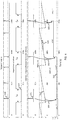
- FIG. 3 shows the rejection of triggers/photons outside the predetermined time window tw when measuring over many periods, according to embodiments of the present invention.
- FIG. 4 shows the use of a voltage ramp with slope m 129 in the time window tw and its sampling events 180, 181 & 182, updating the exponential moving average (EMA) voltage according to embodiments of the present invention.
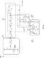
- FIG. 5 , shows an embodiment of a circuit implementation of the present invention having a single photon detection circuit 150, a non-overlapping switch-enable circuit 155, a pulse-inhibit circuit 166 and a switched-capacitor circuit 160.
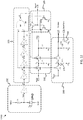
- FIG. 6 , shows an embodiment of a preferred circuit implementation of the present invention having a single photon detection circuit 150, a non-overlapping switch-enable circuit 155, a pulse-inhibit circuit 165 and a switched-capacitor circuit 160.
- FIG. 7 , demonstrates the particular operation of the switched-capacitor circuit 160 according to embodiments of the present invention, driven by non-overlapping switch-enable signals 125 & 126, sampling from the ramp signal 122 and updating the exponential moving average EMA voltage curve 123.
- FIG. 8 shows a simulation demonstrating the exponential moving average based on a statistical model according to embodiments of the present invention.
- FIG. 9 , embodies a circuit whereby two exponential moving averages are computed in two different time windows by a single non-overlapping switch-enable circuit 155, two distinct inhibit circuits 165 and 167, and two distinct switched- capacitor circuits 160 and 162, leading to two exponential moving averages EMA1 and EMA2, according to embodiments of the present invention.
- FIG. 10 , illustrates a definition of two time-windows t w1 111, and t w2 112, that measure two centers of mass tcm1 and tcm2, according to the circuit in FIG. 9 , allowing estimation of the lifetime τ, whilst eliminating the effect of the background light Ibg.
- FIG. 11 illustrates a definition of a first window t w1 111 for measuring fluorescence lifetime τ and a second window t w3 113, useful to estimate the effect of delays of the traveling of the fluorescence light and the signals in the electrical transmission lines in order to derive an approximate value for the delay td.
- FIG. 12 illustrates a circuit that embodies that beside the center of mass also the number of arrived photons in the time window can be counted using event counter 168, according to embodiments of the present invention
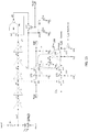
- FIG. 13 illustrates a circuit wherein the weight of the exponential moving averaging can be run-time adapted locally to the number of counted incident photons, according to embodiments of the present invention, using adaptive-weighing circuit 169.
- FIG. 14 shows an example of a definition of windows tw1, tw4 and tw5 for measuring fluorescence light that contains two fluorescence lifetimes τ1 and τ2, possibly due to the presence of two different fluorophores in the illuminated region. For achieving those measurements in parallel in hardware on a per pixel base, the circuit of FIG. 9 can be complemented by an additional third inhibit circuit and switched-capacitor circuit (not shown).
-
The drawings are only schematic and are non-limiting. In the drawings, the size of some of the elements may be exaggerated and not drawn on scale for illustrative purposes. The dimensions and the relative dimensions do not necessarily correspond to actual reductions to practice of the invention. In the different figures, the same reference numbers refer to the same or analogous elements.
Detailed description of the invention
-
The present invention will be described with respect to particular embodiments and with reference to certain drawings, but the invention is not limited thereto but only by the claims. Any reference signs in the claims shall not be construed as limiting the scope.
-
The terms first, second and the like in the specification, are used for distinguishing between similar elements and not necessarily for describing a sequence, either temporally, spatially, in ranking or in any other manner. It is to be understood that the terms so used are interchangeable under appropriate circumstances and that the embodiments of the invention described herein are capable of operation in other sequences than described or illustrated herein.
-
It is to be noticed that the term "comprising", used in the claims, should not be interpreted as being restricted to the means listed thereafter. Thus, the scope of the expression "a device comprising means A and B" should not be limited to devices consisting only of components A and B. It means that with respect to the present invention, the most relevant components of the device are A and B.
-
Similarly, it is to be noticed that the term "coupled" should not be interpreted as being restricted to direct connections only. Thus, the scope of the expression "a device A coupled to a device B" should not be limited to devices or systems wherein an output of device A is directly connected to an input of device B. It means that there exists a path between an output of A and an input of B which may be a path including other devices or means.
-
Reference throughout this specification to "one embodiment" or "an embodiment" means that a particular feature, structure or characteristic described in connection with the embodiment is included in at least one embodiment of the present invention. Thus, appearances of the phrases "in one embodiment" or "in an embodiment" in various places throughout this specification are not necessarily all referring to the same embodiment, but may. Furthermore, the particular features, structures or characteristics may be combined in any suitable manner, as would be apparent to one of ordinary skill in the art from this disclosure, in one or more embodiments.
-
Similarly, it should be appreciated that in the description of exemplary embodiments of the invention, various features of the invention are sometimes grouped together in a single embodiment, figure, or description thereof for the purpose of streamlining the disclosure and aiding in the understanding of one or more of the various inventive aspects. This method of disclosure, however, is not to be interpreted as reflecting an intention that the claimed invention requires more features than are expressly recited in each claim. Rather, as the following claims reflect, inventive aspects lie in less than all features of a single foregoing disclosed embodiment. Thus, the claims following the detailed description are hereby expressly incorporated into this detailed description, with each claim standing on its own as a separate embodiment of this invention.
-
It should be noted that the use of particular terminology when describing certain features or aspects of the invention should not be taken to imply that the terminology is being re-defined herein to be restricted to include any specific characteristics of the features or aspects of the invention with which that terminology is associated.
-
In the description provided herein, numerous specific details are set forth. However, it is understood that embodiments of the invention may be practiced without these specific details. In other instances, well-known methods, structures and techniques have not been shown in detail in order not to obscure an understanding of this description.
DEFINITIONS
-
Fluorescence is the emission of light by a fluorophore that has absorbed electromagnetic excitation radiation, for example light, upon excitation therewith. In most cases, the emitted light has a longer wavelength, and therefore lower photon energy, than the absorbed excitation radiation.
-
Fluorescence lifetime is a measure of the time a fluorophore spends in the excited state before returning to the ground state by emitting a photon. The lifetime of a fluorophore can range from picoseconds to hundreds of nanoseconds.
-
Fluorescence-lifetime imaging microscopy (FLIM) is a technique for producing an image based on differences in exponential decay rate of fluorescence from a fluorescent sample. The lifetime of a fluorophore signal, rather than its intensity, is used to create the image in FLIM. Many other applications (that are not necessarily called FLIM) are in need of fluorescence-lifetime imaging, for example in image guided surgery and biomedical applications, where lifetime gives additional information about the chemical/biological environment of the fluorophore.
-
When a fluorophore gets hit, e.g. illuminated, by a pulse of electromagnetic radiation, e.g. a light-pulse, that excites its internal state, electrons will move to a higher energy state for some time. They will go back to their original state by emitting photons or heat, in an exponential decay process characterized by the fluorophore's fluorescence lifetime. The average time the fluorophore stays in its excited state and emits photons, is called the fluorescence lifetime. In
FIG. 1 , the applied
excitation light 100 is assumed a short and powerful pulse with a predetermined wavelength from a radiation source, e.g. a laser, and with a peak at a stimulation moment
ts. The fluorescent light
105 (typically exhibiting a longer wavelength) starts from the stimulation moment
ts at which the fluorophore is being excited, and after the excitation stops, the
fluorescent light 105 demonstrates a decay that is exponential with the lifetime τ of the fluorophore. The curve of the generated
fluorescent light 105 is on a logarithmic scale a linear curve with a downward
-1/τ slope. One of the known measurement techniques for quantifying the lifetime τ is referred to as the center of mass method. To apply this method, one can define a window period
tw that starts when the
excitation light 100 stopped, e.g. at a first moment
t0, and that preferably is longer than the lifetime to be measured, up to a second moment
t1 (
tw =
t 1 -
t 0). The light emission is then according to the following formula:
with I
0 the intensity of emitted fluorescent light at the first moment t
0.
One can then define the center of mass
tcm as a time period between the first moment
t0 and a center moment
tc according to the following, using first order momentum:
It is generally believed that the measurement window period
tw must be much longer than the fluorophore's lifetime (so
tw >>τ); however, with some math one can find the deviation for the inaccuracy of shorter window periods
tw and compensate for it when necessary.
FIG. 2 shows the
relative compensation 119 one needs to apply. Curve-fitting a simple curve through
119 can easily make this relationship explicit, such that when measuring the center of mass
tcm, and knowing the applied measurement window period
tw, one can deduce the real lifetime τ. In other words, it is also possible to measure a lifetime of e.g. 1 ns, with a window period of e.g. 2 ns using a center of mass method. In what follows it is assumed that by finding the first order momentum
tcm, and knowing the measurement window period
tw, the person skilled in the art can deduct the actual lifetime τ.
-
In an image sensor, wherein the pixels are small, and the number of photons originating from the fluorescent scene is small, one can't rely on a single shot measurement, like the one proposed in FIG. 1 . In reality is very well possible, that only a few photons, or one, or even no photons arrive at the detector during a single window period tw. This complicates the measurement a lot, because one now must re-apply the excitation light pulse 100 many times and collect the data during each window period tw and in some way compute the center of mass tcm from all those trigger events. To make it feasible, in accordance with embodiments of the present invention, a single photon detection circuit 150 will be relied on. Such single photon detection circuit 150 generates a clear digital pulse each time it detects a photon. In order to get enough information, an excitation pulse 100 is re-applied at a repetition rate that is low enough to have a period that is longer than the measurement window period tw. The repetition rate can be chosen freely, but may in practice depend on many elements, such as, but not limited thereto, the performance of the laser, the maximum light intensity that is allowed for eye-safety, and/or the fact that one may get bleaching, whereby the fluorophore gets temporarily saturated or even damaged. Another element that may play a role is the fact that background light also gives photons, and/or that the used detector has its own dark-current (or dark count rate DCR), complicating the measurement even more.
-
In FIG. 3 , curve 101 is the excitation light 100 that is pulsed with a repetition every 60 ns, so at a 16.667 MHz repetition rate. Trigger curve 120 shows trigger/photon events that the used single photon detection 150 circuit outputs when a detector element, for instance a SPAD, detects presence of photons. This includes incoming light from fluorescence, e.g. fluorescent light being emitted by fluorophores having been excited by the excitation light pulses 100 in the curve 101, light from background illumination, and dark counts from the detector itself. In FIG. 3 , six such events occur, but one cannot tell the origin of any of these six events. Nevertheless, it can be assumed for now that the background and dark counts are very low in number compared to the fluorescence light. Reject curve 114 shows three consecutive windows, with a measurement window period tw =20ns, also repeated every 60 ns. When the reject curve signal has a first value, e.g. high, the pulses from the trigger curve 120 are rejected, and when it has a second value, e.g. low, the pulses are allowed into the measurement process, giving the selected trigger curve 121. This cycle can be repeated for e.g. tens of microseconds, or even several milliseconds, all the time passing the pulses only when the reject curve 114 has the second value, e.g. low.
-
Now, in
FIG. 4 , a
voltage ramp signal 122 with slope
m is applied each new measurement window period
tw. This
voltage ramp signal 122 is getting sampled at the moment a selected trigger occurs in the selected
trigger curve 121, giving samples
VS i-2,
VS i-1,
VS i in response to the start of each
event 180, 181 &
182 in the
trigger curve 121. This can be seen as a time-to-analog conversion (TAC), or time-to-voltage conversion, whereby the time is the period from the start of the measurement window period
tw until the event itself, and the analog signal is the sampled voltage
VS i. Sample
VS i is each time used to update the exponentially moving average voltage EMA that resides on a capacitor according to the principles of the "exponential moving average":
-
Averaging-length n is a number that tells how deep the memory into the past is. E.g. with n = 99, at every new sample, the previous result is reused for 99%, and the new sample counts only for a fresh 1%. Samples further in the past become gradually less important, recent samples are more important. The difference with a "simple moving average", is that for achieving the latter, one must keep a list of the last 100 occurrences, and at each new event, one has to drop the value of the oldest event, include the new event, and recalculate the average of the adapted set of 100 events. This takes a lot of computation and memory, and is hard to achieve on a per pixel base in an image sensor.
-
By taking the exponential moving average of time-to-voltage converted samples, a time-domain center-of-mass method is achieved.
-
The EMA curve 123 has a voltage level that is in this particular example three times below the ramp voltage on voltage ramp signal curve 122 at the three events 180, 181 & 182, with as a result, small step increases at each of these moments (in this simulation n=7). In this example one detection event is passed every window; however, it is equally possible that at high light level conditions there are many more events in a same window, and even so, with low light levels, it can happen that there are one, more, or many windows without any event. The voltage ramp signal curve 122 may be, but does not need to be, a perfectly straight line; it should in its window be at least monotonically rising or falling. It can start at zero volt, but it can also start at any other suitable voltage level, as long as the voltages during the ramp are in the operation range of the switches of the attached switched-capacitor circuit 160 (see below). Once the EMA curve 123 gets to convergence, the sampled voltages will statistically kick the EMA voltage up and down, and not always in the same direction as in the three events 180, 181 & 181.
-
FIG. 5 illustrates a fluorescence lifetime determination circuit 500 in accordance with one embodiment of the present invention. The circuit 500 comprises a single photon detection circuit 150 for detecting occurrence of photons, even if they are limited to very limited in number and for correspondingly generating a trigger pulse; a pulse-inhibit circuit 166 for rejecting trigger pulses that occur outside a measurement window; a switched-capacitor circuit 160 for performing an exponential moving average function; and a non-overlapping switch-enable circuit 155 for generating the signals for driving the switched-capacitor circuit 160.
-
The single photon detection circuit 150, in the embodiment illustrated, implements a Single Photon Avalanche Diode (SPAD) detector. The SPAD detector is a semiconductor pn-diode junction that is reversely biased beyond its breakdown voltage, in a metastable state. The SPAD detector is coupled in series with a resistor R1, and this series connection is coupled between a first node 152 and a second node 153. The first node 152 is biased at a first bias voltage Vbias1 and the second node is biased at a second bias voltage Vbias2, Vbias2 being higher than Vbias1 so as to obtain the reverse biasing of the SPAD detector. A single photon can start a breakdown and give a large voltage signal when being biased through the resistor R1, the voltage signal being a temporary voltage drop (Vinput), as can be seen in Fig. 5 . The voltage over the SPAD detector drops until below the SPAD detector's breakdown voltage, whereby the breakdown stops, followed by the diode voltage returning to its original voltage due to the attached resistor R1, the system becoming again metastable. That drop can be detected by a suitable detection circuit, such as an inverter or a comparator circuit (in circuit 150 exemplified, as an example only, the present invention not being limited thereto, with an inverter X1 having a tripping voltage Vtrip ), generating a trigger pulse Vp1 on node p1, the start of the trigger pulse being indicative for the moment that the photon was incident on the detector. Trigger curve 120 in Fig. 3 and Fig. 4 shows six such trigger pulses Vp1 on node p1. There are many types of SPAD detectors and even SPAD circuits, including active ones, (e.g. with active or passive quenching) and types of circuits that are known in the state-of-the-art, and each of them can be used in conjunction with this invention. Single photon detection circuit 150 can include any SPAD or any single photon detector. Common to these circuits is that their output is a digital trigger pulse, of which the start is indicative for the moment of the photon absorption. The width of the trigger pulse is not so meaningful and can often be somewhat variable.
-
Two exemplary systems are described in this specification for inhibiting the pulses outside the measurement windows. The first one, pulse-inhibit circuit 166 in FIG. 5 , implements the rejection of events by lowering the voltage across the SPAD detector. Hereto the pulse-inhibit circuit 166 comprises a variable voltage source 164 coupled between the first node 152 and a third node 154, for example ground. When an input signal Reject to the pulse-inhibit circuit 166, more particularly to the voltage source 164 thereof, is high, an output voltage V1 of the voltage source 164 is adapted, e.g. raised or brought to a higher level, such that the first bias voltage Vbias1 is high, and hence the voltage across the SPAD gets below its breakdown voltage, and breakdowns get prevented. When the input signal Reject to the pulse-inhibit circuit 166, more particularly to the voltage source 164 thereof gets low, an output voltage V1 of the voltage source 164 is adapted, e.g. lowered or brought to a low level, such that the first bias voltage Vbias1 is low, and hence the voltage across the SPAD is again increased, such that breakdown is again possible. The first voltage Vbias1, is often not in the voltage range of the digital power supply range of the sensor logic and modulating the SPAD's bias is therefore not easy to implement in a high-speed way (with tens of picoseconds of precision). Vbias1 is e.g. -20V to achieve SPAD biasing beyond its breakdown voltage, whilst Vbias2 is one or two volts above Vtrip, the tripping voltage of the inverter X1. A more preferred solution that is operative in the digital domain is therefore proposed and explained hereinbelow with reference to FIG. 6 .
-
A switched-capacitor circuit 160 is used for performing an exponential moving average function, as also illustrated in the bottom graph of FIG. 4 . The switched-capacitor circuit 160 as illustrated in FIG. 5 comprises two switches XN1, XN2 coupled in series between an input terminal, ramp terminal 171, and an output terminal, EMA terminal 172. At a sample node 173 between the two switches XN1, XN2, a first capacitor C1 is coupled to ground. At the output terminal 172, a second capacitor C2 is coupled to ground.
-
The switches XN1, XN2 of the switched-capacitor circuit 160 are actuated such that only one of the switches XN1, XN2 is conductive at any moment in time. The driving signals for actuating the switches XN1, XN2 are received from a non-overlapping switch-enable circuit 155 that is explained in more detail below.
-
In the embodiment illustrated in FIG. 5 , the switches XN1, XN2 are implemented by means of NMOS pass-gates. The gates of these NMOS pass-gates are coupled to and receive actuating signals from a non-overlapping switch-enable circuit 155.
-
The non-overlapping switch-enable circuit 155, in particular embodiments of the present invention, comprises an even sequence of inverters which are coupled in series. In this example, there are four inverters X2, X3, X4, X5, with output nodes p2, p3, p4, p5 respectively. Node p2 is the first switch-enable output signal to actuate the first switch XN1 of the switched capacitor circuit 160. This node p2 is also an input to a NOR gate X6 that also has p5 as input. When p1 goes high, p2 goes low, and p5 being low already will go high three inverter delays later. This leave a period of three inverters delays that both inputs of the NOR X6 are low, during which the NOR gate X6 outputs a high on its output p7. This is basically a one-shot circuit: the input p1 goes high (for example during 3 ns), and output p7, goes high for a predetermined short period (e.g. 1 ns), determined by three inverter delays. The output signal of the NOR gate X6 is fed to the second switch XN2 for actuation thereof, for instance to the gate of the NMOS pass-gate. Many alternative one-shot circuits are possible, known to a person skilled in the art.
-
As illustrated in the one but last graph of FIG. 4 , a ramp voltage 122 is used in the performing of the exponential moving average function. The ramp voltage, to be generated externally, is applied at the Ramp terminal 171 and is connected to the source of a first switch XN1, that in the embodiment illustrated, is made by an NMOS pass-gate. The signal Vs at the drain of the first switch XN1, i.e. at the sample node 173, follows the voltage ramp signal 122 ( FIG. 4 ), as long as the gate of the first switch XN1 is biased high, waiting for an event.
-
FIG. 7 is illustrative for this process. The signal corresponding to the passed-on trigger pulse, e.g. the signal on output node
p2 of inverter
X2, is represented by
curve 125, and the signal at output node
p7 of the NOR gate
X6 is represented by
curve 126. Around time= 93 ns, the voltage on node
p2 drops, and the first switch
XN1 stops being conductive. The voltage present at that moment in time at the
sample node 173 is a sample
VS i of the ramp voltage that was applied at that moment in time to the
ramp terminal 171. The sample
VS i is now present/valid and holds that voltage level thanks to capacitor
C1. The signal at node
p7 (curve
126), not overlapping with the signal at node
p2 (curve
125), now goes high, making the second switch (NMOS pass-gate)
XN2 conductive. First and second capacitors
C1 and
C2 get shorted to each other (
curve 124, illustrating the voltage at the
sample node 173, and
curve 123, illustrating the voltage at the
EMA terminal 172, coming together at t=93.5 ns), and a charge sharing redistribution takes place whereby the signal
VS i and the output signal
EMA (curve 123) move to each other determined by the ratio of
C1/C2. If the first capacitor
C1 is hundred times smaller than the second capacitor
C2, then
n=100. The voltage on the
sample node 173 moves approximately 99% towards the voltage at the
EMA terminal 172, and the voltage at the
EMA terminal 172 moves approximately 1% towards the voltage at the
sample node 173. Roughly speaking, one can say that the last 100 samples determine mostly the effective average outcome. In the examples of
FIG. 4 &
7 , then number is chosen quite small
(n=7) making the voltage jumps more easily visible. The following holds approximately:
-
When an output is wanted that has a good precision, n should be taken high, i.e. between 100 and 1000, what increases the number of samples needed for convergence after initialization of the filter, or after a sudden lifetime change. One cannot tell whether this will then take a measuring time of microseconds or milliseconds, because the time it takes to change, entirely depends on the number of incoming photons/events and the n-value. It is an option to keep the number n relatively low, e.g. at 50, and to sample the EMA output from outside the pixel, and to do additional external calculations and averaging, thereby increasing the accuracy and precision in a second step, e.g. with DSP digital processing means.
-
FIG. 8 shows the operation whereby n=50, simulation is run for 200 samples passing the measurement windows with a time distribution generated by a random generator that takes into account an exponential decay behavior with a lifetime of 2.6 ns. The measurement window period tw is set to 10 ns, and the repetition rate to 10 MHz. Bar-chart 141 shows the histogram of the 200 recorded events over the 10 ns window period. Curve 140 is the EMA signal (in this simulation it is in nanoseconds) beginning at a start condition of 0 ns. After 75 samples, a steady state occurs with an average of about 2.4 ns and a precision of 7% on the lifetime (for the samples from 100 till 200). Using curve 119 in FIG. 2 , one can correct for the fact the lifetime is about 1/4th of the sampling window (of 10ns), and that brings the result to close the original 2.6 ns lifetime used for the lifetime distribution sample generation. The precision and the accuracy adapt according to normal statistical rules: for example, when increasing n by a factor of 4, a precision increase of a factor 2 is obtained.
-
In practice, the accompanying circuit that is located in a pixel should be as small as possible, in order for the pixel to have a fill factor as high as possible. It can therefore be advised to omit the first capacitor C1 entirely, and to rely on the remaining parasitic capacitance of the concerned sample node 173. After having an estimate of the parasitic value C1, one can choose C2 to be n times that value. C2 can then be implemented by the person skilled in the art, in the way it fits best into an imager pixel.
-
Circuits in accordance with embodiments of the present invention can deviate largely from the presented ones. However, special care was taken to keep the transistor count low. Also, since most of the operation is in the digital domain, very limited analog difficulties are present. When envisaging a lifetime precision of 1%, it is also sufficient to have a low precision ADC (e.g. 8 bit) for conversion of the EMA voltage. The width and length (W/L values) of the transistors are not critical, and can be determined by the person skilled in the art. Most transistors can be of minimal width and length; however, one must check that curves 125 and 126 ( FIG. 7 ) remain non-overlapping, and preferably reach the full power supply voltage, i.e. to make sure that the switches of the switched-capacitor circuit 160 operate optimally or at least sufficiently good.
-
As stated before, a more preferred solution for the pulse-inhibit circuit than the one explained with reference to FIG. 5 is operative in the digital domain. FIG. 6 illustrates a fluorescence lifetime determination circuit 600 in accordance with embodiments of the present invention, including a digital domain pulse-inhibit circuit 165. Besides this pulse-inhibit circuit 165, the circuit 600 includes a single-photon detection circuit 150, a non-overlapping switch-enable circuit 155, and a switched-capacitor circuit 160. These latter components are as disclosed with respect to FIG. 5 , and they are not explained again in detail here.
-
In the embodiment of FIG. 6 , one of the signals driving the switched-capacitor circuit 160 can be intercepted, in that way preventing a pulse to be taken into account for performing the averaging. This is demonstrated in FIG. 6 wherein the pulse inhibit circuit 165 deletes in response to gating signal Reject unwanted pulses on the output node p6 of the NOR-gate X6 that fall outside the measurement windows tw, and delivers a cleaned version of the signal on node p6 on node p7 going to pass-gate XN2 of the switched-capacitor circuit 160. In FIG. 4 the signal on node p6 is given in curve 120, and the cleaned version, i.e. the version with pulses outside the measurement windows tw is given in curve 121. Inhibit circuit 165 as depicted in Fig. 6 can also be made in different ways, e.g. also by including an AND gate (not shown).
-
One of the nice features of the preferred solution presented in FIG. 6 is that, as illustrated in the detector 900 of FIG. 9 , with only an additional 5 transistors and two capacitors a second EMA2 switched-capacitor circuit 162 with its own time window and same or different voltage ramp signal Ramp2, and second pulse-inhibit circuit 167 may be fabricated that can operate entirely independent of (but simultaneously with) the first EMA1 switched-capacitor circuit 160 and pulse-inhibit circuit 165. In image sensors, the area of additional circuitry has to be kept low, because in lower cost monolithic solutions, the area that circuitry occupies is in trade-off with that for the actual light detection area. Due to the small required area the number of center-of-mass measurements that operate in parallel can be increased, in which sampled photons can be allowed or inhibited depending on dedicated applied windows ...
-
FIG. 10 shows a very useful application of performing measuring two centers of mass of the input light. In the case there is also background light, that is uncorrelated to the
excitation light 100, one gets a light reception that has following behavior:
-
Ibg is the background light component that generates events at random moments in the input signal. The center of mass t cm1 in the first measurement window 111 with a first, shorter, measurement period t w1, starting at time t0 and ending at time t1, is going to be distorted towards the center of the window (i.e. closer to t w1 /2) due to these random events. By including a second center of mass measurement based on a second measurement window 112 that also starts at time t0 but that ends at time t2 later than time t1, hence with a second, longer, measurement period t w2 taken e.g. twice as long as the first window t w1, one has an extra equation to which the system needs to adhere. In this way there are two equations with two unknowns: lifetime τ and background light Ibg. Persons skilled in art can accurately retrieve the lifetime stripped from the background light interference by solving these equations. The precision on the outcome will be somewhat reduced due to the shot-noise of the background light, which can't be avoided.
-
In embodiments of the present invention, single photon detection circuits 150 may have elevated dark count rates (DCR), giving the same effect as background light. DCR can thus be treated in the same way, using a double center of mass approach as explained with respect to FIG. 10 . Measuring multiple centers of mass can be achieved in parallel, using extra circuitry on board of each pixel in an image sensor as just mentioned, or, consecutively, assuming non changing conditions in the scene, one after the other using the same circuitry. A combination can also be anticipated, e.g. measuring first two centers of mass in parallel, and then another two centers of mass, when hardware is only equipped for two in parallel.
-
FIG. 11 shows another use of the double center of mass approach. In a lifetime measurement with short lifetimes of the order of nanoseconds, each signal transmission in the set-up has a substantial delay, be it for electrical signals, travelling at 60-70% of the light velocity, or the light itself. To achieve best precision and accuracy, it is always preferred to position the measurement window starting at t 0, not too much after the maximum moment ts of the fluorescence light 107. Therefore, it is useful to first find the delay td between the excitation pulse and the actual emission of fluorescent light, being function of all involved transmission lines, pathways of light, and on the whole synchronisation principle in the implemented system. A further measurement window with a starting moment t3, conveniently chosen such that one is certain that t3 is before ts, the starting time of emission of fluorescent light, and with measurement window period t w3, is put in place. In the example illustrated in FIG. 11 , the further measurement window has an end time t1, just like the other measurement window used, which has a starting time t0 and end time t1. The measured center of mass tcm3 of the further measurement window will point to the moment in time tc3, that will be beyond the starting time ts of emission of fluorescent light, and an estimate can then be made to roughly locate ts.
-
FIG. 12 shows that a fluorescence lifetime determination circuit 1200 in accordance with embodiments of the present invention can conveniently include an analog photon-counter circuit 168, giving information about the number of events passing the measurement window periods, since a moment when a reset pulse on a ResetCount input has been applied.
-
The photon-counter circuit 168 illustrated in FIG. 12 is only one embodiment of a possible implementation. It comprises a series connection of pass-gate switches X12, X22, for instance NMOS pass-gate switches, with a counter sampling node 175 between both pass-gate switches X12, X22. A sampling capacitor C12 is coupled between ground and the counter sampling node 175. The source side of the first pass-gate switch X12 is coupled to a fixed voltage VSX12 below Vdd, not shown, and the drain side of the second pass-gate switch X22 is coupled to an output node Countout. A further capacitor C22 is coupled between ground and the drain of the second pass-gate switch X22. The first and second pass-gate switches X12, X22 are actuated by the same signals which also actuate pass-gates XN1, XN2 in the switched-capacitor circuit 160, e.g. these signals are fed to the gates of the pass-gate switches X12, X22.
-
When no trigger pulse occurs, the signal at the gate of pass-gate X12 is the signal at node p2, and this signal is high. The voltage level Vsc at the drain side of pass-gate X12 then equals VSX12. When a trigger pulse occurs, this voltage at the counter sampling node 175 is sampled.
-
The signal at node p7, not overlapping with the signal at node p2, now goes high, making the second pass-gate switch X22 conductive. The capacitors C12 and C22 get shorted to each other, and a charge sharing redistribution takes place whereby the signal at the counter sampling node 175 and the signal at the output node Countout move to each other determined by the ratio of C22/C12.
-
This way, the voltage at the output node Countout steps up, every time such events happens, but in a saturating way: every step on Countout will be a bit smaller, and in the end, a saturation voltage close to VSX12. This counter number at saturation depends on the chosen capacitor ratio C22/C12. C12 can be entirely made-up of its parasitic node, keeping the circuit small. One can implement counter values between ten and a few hundreds, without needing a too large capacitor C22.
-
A reset switch 700 is coupled between the output node Countout and ground, for resetting the output node Countout. The reset switch 700 may for instance be a transistor, the gate of which is coupled to an externally applied signal ResetCount.
-
Sometimes it is known that the EMA average voltage is not yet converged, e.g. right after start-up, or when a different lifetime is suddenly present. In that case, it is possible to speed-up the convergence process by temporarily lowering the n-number of the switched capacitor circuit 160. In fact, by changing the value of capacitor C1, averaging-length n can be modulated in a convenient way. This can be done by externally adding capacitors to the sample node 173. However, averaging-length n can also be linked to the number of photons that passed the window, making use of a photon counter 168. In FIG. 13 this is demonstrated in following way: a circuit 169 monitors whether a predetermined number of photons has been counted after the reset-pulse on input ResetCount. Before that, an external capacitor C3 is added to the first capacitor C1 of the switched-capacitor circuit 160 by means of a switch X9. The averaging-length n is short, and the EMA moves quickly, giving a rough and quick estimation of the center of mass. After that, the external capacitor C3 is detached because the actuation signal to the gate of switch X9 (at node p8) goes low, and averaging length n is increased, leading to a more precise measurement starting then from the rough approximate first estimate. In this way, curve 140 of FIG. 8 , could have a much steeper slope, e.g. and instead of needing 75 samples to reach the rough estimate, get there in 10 steps. The circuit in FIG. 13 works in a digital way, but of course more advanced solutions leading to a softer increase in averaging-length n can be made by the person skilled in the art. E.g., one can make use of the variability of the channel capacitance of a transistor or use a dedicated varactor.
-
Sometimes, one has a combination of fluorophores that output two lifetimes upon stimulation:
In this case, three unknowns need to be found, being the first lifetime τ
1, the second lifetime τ
2 and the ratio of the intensities of emitted fluorescent light at the first moment to
I 1/
I 0.
-
If this is the case, finding three centers of mass is required. To solve this, one must choose three measurement windows in a strategic way. As an example, FIG. 14 shows an option for these three measurement windows, a first measurement window t w1, a second measurement window t w4 which falls later in time, and a third measurement window t w5 which is as long as the first and second measurement windows together.
-
The shorter lifetime will mostly influence the center of mass in the first measurement window t w1. The longer lifetime will mostly influence the center of mass in the second measurement window t w4, and the center of mass in t w5 will be largely influenced by each of the three unknowns. Anyhow, the person skilled in the art can solve the three equations based on the three measured centers of mass and find the three unknowns in the way he/she prefers most. Adding the possibility of having also non-negligible background light or DCR (of the single photon detection circuit 150), this would add yet another unknown variable that can retrieved by an additional center of mass measurement window (not illustrated) and its mathematical equation (having 4 unknowns and 4 equations).
-
Any of the systems that are presented here, or that are based on it, can be complemented by other means known in the state of the art in image sensors. For example, one can apply micro-lenses, colour filters, to improve qualitatively, or quantitatively the light input to the single photon detection circuit. Any means for improving the internal/external quantum efficiency, responsivity, and detection probability can be applied. Three-dimensional stacking can be done, e.g. whereby a SPAD detector layer stems from another wafer/material then the CMOS circuit wafer. Back-side illumination (BSI) can be applied, current assistance can be applied or an Silicon On Insulator (SOI) can be favoured. The proposed embodiments of the invention can be laid out as pixels for a sensor array, in total constituting an image sensor for fluorescence lifetime and fluorescence light intensity acquisition. For each read-out voltage node, a voltage-follower transistor, can be provided, with a row-select transistor for row-based read-out, as is often done in CMOS image sensors. Several signals can be grouped for a plurality of pixels, or are the same for a whole array, like the ones defining the windows (Reject), the Ramp signal(s), reset signal(s), and signals determining the averaging-length n. In addition to all this, a standard 3T or 4T image sensor pixel can be added, for performing simultaneously standard image sensing. The single-photon detection circuit 150 may contain a regular SPAD, but can also contain any other means to achieve single photon detection, including an avalanche photodetector (APD) with so much gain, that one can use the linear gain modus to operate the diode below break-down and still achieve digital photon arrival pulses.
-
While the invention has been illustrated and described in detail in the drawings and foregoing description, such illustration and description are to be considered illustrative or exemplary and not restrictive. The foregoing description details certain embodiments of the invention. It will be appreciated, however, that no matter how detailed the foregoing appears in text, the invention may be practiced in many ways. The invention is not limited to the disclosed embodiments.