EP3933940A1 - Method for manufacturing multi-layered thin film, method for manufacturing solar cell, and method for manufacturing solar cell module - Google Patents
Method for manufacturing multi-layered thin film, method for manufacturing solar cell, and method for manufacturing solar cell module Download PDFInfo
- Publication number
- EP3933940A1 EP3933940A1 EP20763204.3A EP20763204A EP3933940A1 EP 3933940 A1 EP3933940 A1 EP 3933940A1 EP 20763204 A EP20763204 A EP 20763204A EP 3933940 A1 EP3933940 A1 EP 3933940A1
- Authority
- EP
- European Patent Office
- Prior art keywords
- photoelectric conversion
- solar cell
- conversion layer
- film
- less
- Prior art date
- Legal status (The legal status is an assumption and is not a legal conclusion. Google has not performed a legal analysis and makes no representation as to the accuracy of the status listed.)
- Granted
Links
Images




Classifications
-
- C—CHEMISTRY; METALLURGY
- C23—COATING METALLIC MATERIAL; COATING MATERIAL WITH METALLIC MATERIAL; CHEMICAL SURFACE TREATMENT; DIFFUSION TREATMENT OF METALLIC MATERIAL; COATING BY VACUUM EVAPORATION, BY SPUTTERING, BY ION IMPLANTATION OR BY CHEMICAL VAPOUR DEPOSITION, IN GENERAL; INHIBITING CORROSION OF METALLIC MATERIAL OR INCRUSTATION IN GENERAL
- C23C—COATING METALLIC MATERIAL; COATING MATERIAL WITH METALLIC MATERIAL; SURFACE TREATMENT OF METALLIC MATERIAL BY DIFFUSION INTO THE SURFACE, BY CHEMICAL CONVERSION OR SUBSTITUTION; COATING BY VACUUM EVAPORATION, BY SPUTTERING, BY ION IMPLANTATION OR BY CHEMICAL VAPOUR DEPOSITION, IN GENERAL
- C23C14/00—Coating by vacuum evaporation, by sputtering or by ion implantation of the coating forming material
- C23C14/06—Coating by vacuum evaporation, by sputtering or by ion implantation of the coating forming material characterised by the coating material
- C23C14/08—Oxides
-
- C—CHEMISTRY; METALLURGY
- C23—COATING METALLIC MATERIAL; COATING MATERIAL WITH METALLIC MATERIAL; CHEMICAL SURFACE TREATMENT; DIFFUSION TREATMENT OF METALLIC MATERIAL; COATING BY VACUUM EVAPORATION, BY SPUTTERING, BY ION IMPLANTATION OR BY CHEMICAL VAPOUR DEPOSITION, IN GENERAL; INHIBITING CORROSION OF METALLIC MATERIAL OR INCRUSTATION IN GENERAL
- C23C—COATING METALLIC MATERIAL; COATING MATERIAL WITH METALLIC MATERIAL; SURFACE TREATMENT OF METALLIC MATERIAL BY DIFFUSION INTO THE SURFACE, BY CHEMICAL CONVERSION OR SUBSTITUTION; COATING BY VACUUM EVAPORATION, BY SPUTTERING, BY ION IMPLANTATION OR BY CHEMICAL VAPOUR DEPOSITION, IN GENERAL
- C23C14/00—Coating by vacuum evaporation, by sputtering or by ion implantation of the coating forming material
- C23C14/22—Coating by vacuum evaporation, by sputtering or by ion implantation of the coating forming material characterised by the process of coating
- C23C14/34—Sputtering
-
- H—ELECTRICITY
- H10—SEMICONDUCTOR DEVICES; ELECTRIC SOLID-STATE DEVICES NOT OTHERWISE PROVIDED FOR
- H10F—INORGANIC SEMICONDUCTOR DEVICES SENSITIVE TO INFRARED RADIATION, LIGHT, ELECTROMAGNETIC RADIATION OF SHORTER WAVELENGTH OR CORPUSCULAR RADIATION
- H10F10/00—Individual photovoltaic cells, e.g. solar cells
- H10F10/10—Individual photovoltaic cells, e.g. solar cells having potential barriers
- H10F10/16—Photovoltaic cells having only PN heterojunction potential barriers
-
- H—ELECTRICITY
- H10—SEMICONDUCTOR DEVICES; ELECTRIC SOLID-STATE DEVICES NOT OTHERWISE PROVIDED FOR
- H10F—INORGANIC SEMICONDUCTOR DEVICES SENSITIVE TO INFRARED RADIATION, LIGHT, ELECTROMAGNETIC RADIATION OF SHORTER WAVELENGTH OR CORPUSCULAR RADIATION
- H10F10/00—Individual photovoltaic cells, e.g. solar cells
- H10F10/10—Individual photovoltaic cells, e.g. solar cells having potential barriers
- H10F10/17—Photovoltaic cells having only PIN junction potential barriers
- H10F10/172—Photovoltaic cells having only PIN junction potential barriers comprising multiple PIN junctions, e.g. tandem cells
-
- H—ELECTRICITY
- H10—SEMICONDUCTOR DEVICES; ELECTRIC SOLID-STATE DEVICES NOT OTHERWISE PROVIDED FOR
- H10F—INORGANIC SEMICONDUCTOR DEVICES SENSITIVE TO INFRARED RADIATION, LIGHT, ELECTROMAGNETIC RADIATION OF SHORTER WAVELENGTH OR CORPUSCULAR RADIATION
- H10F10/00—Individual photovoltaic cells, e.g. solar cells
- H10F10/10—Individual photovoltaic cells, e.g. solar cells having potential barriers
- H10F10/19—Photovoltaic cells having multiple potential barriers of different types, e.g. tandem cells having both PN and PIN junctions
-
- H—ELECTRICITY
- H10—SEMICONDUCTOR DEVICES; ELECTRIC SOLID-STATE DEVICES NOT OTHERWISE PROVIDED FOR
- H10F—INORGANIC SEMICONDUCTOR DEVICES SENSITIVE TO INFRARED RADIATION, LIGHT, ELECTROMAGNETIC RADIATION OF SHORTER WAVELENGTH OR CORPUSCULAR RADIATION
- H10F19/00—Integrated devices, or assemblies of multiple devices, comprising at least one photovoltaic cell covered by group H10F10/00, e.g. photovoltaic modules
- H10F19/30—Integrated devices, or assemblies of multiple devices, comprising at least one photovoltaic cell covered by group H10F10/00, e.g. photovoltaic modules comprising thin-film photovoltaic cells
- H10F19/31—Integrated devices, or assemblies of multiple devices, comprising at least one photovoltaic cell covered by group H10F10/00, e.g. photovoltaic modules comprising thin-film photovoltaic cells having multiple laterally adjacent thin-film photovoltaic cells deposited on the same substrate
-
- H—ELECTRICITY
- H10—SEMICONDUCTOR DEVICES; ELECTRIC SOLID-STATE DEVICES NOT OTHERWISE PROVIDED FOR
- H10F—INORGANIC SEMICONDUCTOR DEVICES SENSITIVE TO INFRARED RADIATION, LIGHT, ELECTROMAGNETIC RADIATION OF SHORTER WAVELENGTH OR CORPUSCULAR RADIATION
- H10F71/00—Manufacture or treatment of devices covered by this subclass
-
- H—ELECTRICITY
- H10—SEMICONDUCTOR DEVICES; ELECTRIC SOLID-STATE DEVICES NOT OTHERWISE PROVIDED FOR
- H10F—INORGANIC SEMICONDUCTOR DEVICES SENSITIVE TO INFRARED RADIATION, LIGHT, ELECTROMAGNETIC RADIATION OF SHORTER WAVELENGTH OR CORPUSCULAR RADIATION
- H10F77/00—Constructional details of devices covered by this subclass
- H10F77/10—Semiconductor bodies
- H10F77/12—Active materials
-
- Y—GENERAL TAGGING OF NEW TECHNOLOGICAL DEVELOPMENTS; GENERAL TAGGING OF CROSS-SECTIONAL TECHNOLOGIES SPANNING OVER SEVERAL SECTIONS OF THE IPC; TECHNICAL SUBJECTS COVERED BY FORMER USPC CROSS-REFERENCE ART COLLECTIONS [XRACs] AND DIGESTS
- Y02—TECHNOLOGIES OR APPLICATIONS FOR MITIGATION OR ADAPTATION AGAINST CLIMATE CHANGE
- Y02E—REDUCTION OF GREENHOUSE GAS [GHG] EMISSIONS, RELATED TO ENERGY GENERATION, TRANSMISSION OR DISTRIBUTION
- Y02E10/00—Energy generation through renewable energy sources
- Y02E10/50—Photovoltaic [PV] energy
- Y02E10/548—Amorphous silicon PV cells
Definitions
- Embodiments described herein relate generally to a method for manufacturing a stacked thin film, a method for manufacturing a solar cell, and a method for manufacturing a solar cell module.
- Tandem solar cells are more efficient than unijunction solar cells because tandem solar cells include cells having higher spectral sensitivity for each wavelength range.
- One of prospective materials for the top cells of tandem solar cells is a cuprous oxide compound, which is inexpensive and has a wide band gap.
- Some conventional cuprous oxide solar cells made of oxidized copper foils have been reported to achieve an efficiency of approximately 8%; however, this efficiency is lower than the theoretical efficiency limit. This is considered to be poor pn junctions caused by heterogeneous substances such as copper oxide that have not been removed sufficiently by etching from the uppermost surfaces after the oxidization of copper foils, or residual elements of etching solution.
- a method for manufacturing a stacked thin film of an embodiment includes forming a photoelectric conversion layer on a first transparent electrode by sputtering using a target mainly composed of copper in an oxygen containing atmosphere.
- An oxygen partial pressure of the sputtering is in a range of 0.01 [Pa] or more and 4.8 [Pa] or less, and 0.24 ⁇ d [Pa] or more and 2.4 ⁇ d [Pa] or less when a deposition rate is d [ ⁇ m/min], in formation of the photoelectric conversion layer.
- a sputtering temperature is 300°C or more and 600°C or less, in formation of the photoelectric conversion layer.
- FIG. 1 is a schematic cross-sectional view of a stacked thin film 100.
- a stacked thin film 100 of FIG. 1 includes a first transparent electrode 1 and a photoelectric conversion layer 2 formed on the first transparent electrode 1.
- the first transparent electrode 1 constitutes a stacked structure together with the photoelectric conversion layer 2.
- the first transparent electrode 1 is in direct contact with the photoelectric conversion layer 2.
- the main surface of the first transparent electrode 1 faces the main surface of the photoelectric conversion layer 2, and these two main surfaces share an interface. It is preferable that the entire surface of the photoelectric conversion layer 2, which faces the first transparent electrode 1, be in direct contact with the first transparent electrode 1.
- the first transparent electrode 1 is a p-type electrode in direct contact with the photoelectric conversion layer 2, which is also p-type. It is preferable that the first transparent electrode 1 have a thickness of 100 nm or more and 1000 nm or less, for example.
- the first transparent electrode 1 include a transparent electrically-conductive oxide film.
- Materials for the transparent electrically-conductive oxide film include, but not limited to, indium tin oxide (ITO), Al-doped zinc oxide (AZO), boron-doped zinc oxide (BZO), gallium-doped zinc oxide (GZO), fluorine-doped tin oxide (FTO), antimony-doped tin oxide (ATO), titanium-doped indium oxide (ITiO), indium zinc oxide (IZO), indium gallium zinc oxide (IGZO), Ta-doped tin oxide (SnO 2 :Ta), Nb-doped tin oxide (SnO 2 :Nb), W-doped tin oxide (SnO 2 :W), Mo-doped tin oxide (SnO 2 :Mo), F-doped tin oxide (SnO 2: F), and hydrogen-doped indium oxide (IOH).
- ITO
- Such a transparent electrically-conductive oxide film may be a stacked film including a plurality of films and include a tin oxide film other than the above oxides.
- Dopants for films such as the tin oxide film include, but not limited to, one or more substances selected from the group including In, Si, Ge, Ti, Cu, Sb, Nb, F, Ta, W, Mo, Br, I, and Cl. It is preferable that the photoelectric conversion layer 2 be in direct contact with the transparent electrically-conductive oxide film included in the first transparent electrode 1.
- the first transparent electrode 1 have a stacked structure in which an indium tin oxide film and a doped tin oxide film are stacked on each other. Specifically, it is preferable that the first transparent electrode 1 have one or more stacked structures selected from the group including a stacked film of an indium tin oxide film and an antimony-doped tin oxide film, a stacked film of an indium tin oxide film and a fluorine-doped tin oxide film, a stacked film of an indium tin oxide film and a Ta-doped tin oxide film, and a stacked film of an indium tin oxide film and a Nb-doped tin oxide film.
- the doped tin oxide film be in direct contact with the photoelectric conversion layer 2.
- the first transparent electrode 1 may include a metal film having a thickness equal to or less than 10 nm.
- the metal film includes, but not limited to, one or more films selected from the group including Mo, Au, Cu, Ag, Al, Ta, Pt, Ru, and W.
- the first transparent electrode 1 may be an electrode including metal in a dot form, a line form, or a mesh form on the top or bottom of the transparent electrically-conductive oxide film. In this case, the metal in a dot form, a line form, or a mesh form is disposed between the transparent electrically-conductive oxide film and the photoelectric conversion layer 32.
- the metal in a dot form, a line form, or a mesh form have an aperture ratio equal to or more than 50% with respect to the transparent electrically-conductive oxide film.
- the metal in a dot form, a line form, or a mesh form includes, but not limited to, Mo, Au, Cu, Ag, Al, Ta, Pt, Ru, and W. Because providing the metal in a dot form, a line form, or a mesh form ensures transparency, the metal film may have any thickness.
- the surface of the first transparent electrode 1 on which the photoelectric conversion layer 2 will be formed be a thin film of a metallic oxide mainly composed of Sn (a transparent electrically-conductive oxide film). It is preferable that Sn account for 90 atom% or more in the metal of the metallic oxide mainly composed of Sn.
- the metallic oxide thin film mainly composed of Sn may contain one or more metals (metallic oxides) selected from the group consisting of Zn, Al, Ga, In, Si, Ge, Ti, Cu, Sb, Nb, F, and Ta other than Sn.
- a metallic oxide mainly composed of In e.g. ITO
- the stacked boy of the ITO film and the substrate is easily deformed due to a high temperature. Therefore, an ITO film is not suitable for the direct formation of a Cu 2 O film thereon.
- the photoelectric conversion layer 2 is a p-type compound semiconductor layer mainly composed of cuprous oxide.
- Cuprous oxide is represented by Cu 2 O and is an oxide semiconductor. Cuprous oxide is non-doped or doped cuprous oxide.
- the photoelectric conversion layer 2 has a thickness of 500 nm or more and 10 ⁇ m or less, for example.
- the thickness of the photoelectric conversion layer 2 is preferably 1000 nm or more and 5 ⁇ m or less, and more preferably 1500 nm or more and 3 ⁇ m or less.
- the thickness of the photoelectric conversion layer 2 can be determined through cross-section observation, for example.
- the photoelectric conversion layer 2 have many large cuprous oxide crystals and contribute to excellent conversion efficiency and light transparency of a solar cell including the stacked thin film 100.
- the stacked thin film 100 manufactured by the method according to an embodiment of the present disclosure will have large cuprous oxide crystals and contribute to the improved conversion efficiency and light transparency.
- the photoelectric conversion layer 2 contain cuprous oxide at 95wt% or more. It is preferable that the photoelectric conversion layer 2 contain cuprous oxide at 98wt% or more. In other words, it is preferable that the photoelectric conversion layer 2 contain almost no (substantially little) heterogeneous substances such as CuO and Cu.
- the photoelectric conversion layer 2 containing almost no heterogeneous substances such as CuO and Cu and being a substantially homogeneous Cu 2 O thin film has very high light transparency, which is preferable.
- a photo luminescence (PL) method can be used for determining whether the photoelectric conversion layer 2 is a substantially homogeneous Cu 2 O thin film or not.
- the photoelectric conversion layer 2 contain Cu of 60.0 atom% or more and 67.0 atom% or less and O (oxygen) of 32.5 atom% or more and 34.0 atom% or less.
- the photoelectric conversion layer 2 may contain an element selected from the group including metals other than Cu, dopants, and impurities, except Cu and O (oxygen).
- the photoelectric conversion layer 2 may contain a metal other than Cu as an oxide and be a complex oxide.
- the metals contained in the photoelectric conversion layer 2 include one or more metals selected from the group including Sn, Sb, Ag, Li, Na, K, Cs, Rb, Al, Ga, In, Zn, Mg, and Ca, in addition to Cu.
- the photoelectric conversion layer 2 contains one or more metals selected from the group including Ag, Li, Na, K, Cs, Rb, Al, Ga, In, Zn, Mg, Ta, and Ca, in addition to Cu; the band gap of the photoelectric conversion layer 2 can be adjusted.
- the photoelectric conversion layer 2 may have a p+ region containing one or more p-type dopants selected from Si, Ge, and N at a high content on the side adjacent to the first transparent electrode 1.
- the band gap of the photoelectric conversion layer 2 be 2.0 eV or more and 2.2 eV or less.
- the band gap in this range will enable both the top cell and the bottom cell to efficiently use solar energy.
- the composition of the photoelectric conversion layer 2 can be represented by Cu a M b O c .
- M represents one or more elements selected from the group including Si, Ge, N, Sn, Sb, Ag, Li, Na, K, Cs, Rb, Al, Ga, In, Zn, Mg, Ta, and Ca.
- the above composition ratio of the photoelectric conversion layer 2 is the composition ratio of the entire photoelectric conversion layer 2. In addition, it is preferable that the above compound composition ratio of the photoelectric conversion layer 2 be met in the entire photoelectric conversion layer 2.
- the photoelectric conversion layer 2 may contain additive(s) other than the above substances.
- FIG. 2 is a flowchart showing the method for manufacturing the stacked thin film 100.
- the method for manufacturing the stacked thin film 100 includes a step (S01) for forming the photoelectric conversion layer 2 on the first transparent electrode 1 by sputtering using a target mainly composed of copper in an atmosphere at an oxygen partial pressure of 0.01 [Pa] or more and 10 [Pa] or less.
- the method may optionally include a step (S00) for pressure reduction.
- the target mainly composed of copper has a copper purity equal to or more than 99.99%.
- the copper purity is preferably equal to or more than 99.995%, more preferably equal to or more than 99.999%.
- the target having a high cupper purity provides the substantially homogeneous Cu 2 O photoelectric conversion layer 2.
- the cupper purity may be different.
- the sputtering atmosphere is preferably an oxidizing atmosphere in which inert gas and oxygen gas are mixed.
- the sputtering atmosphere is more preferably an atmosphere of inert gas and oxygen gas.
- the inert gas is preferably nitrogen gas, argon gas, or mixed gas of nitrogen gas and argon gas.
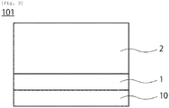
- FIG. 3 is a schematic cross-sectional view of a stacked thin film 100 including the substrate 10. Sputtering is performed on the first transparent electrode 1 so that the photoelectric conversion layer 2 is deposited on the first transparent electrode 1.
- the step (S00) be taken for reducing the pressure in the chamber where the first transparent electrode 1 is disposed to 5.0 ⁇ 10 -3 [Pa] or less.
- the step (S00) for pressure reduction may be taken in a chamber for sputtering or a subchamber for sputtering.
- the substrate 10 can be used for a substrate for a solar cell including the thin film 100.
- the first transparent electrode 1 is formed on the substrate 10 by e.g. sputtering. It is preferable that the substrate 10 be made of glass such as white sheet glass, soda-lime glass, chemically strengthened glass, and quartz glass.
- the substrate 10 may be made of an organic material such as acryl, polycarbonate, and polyimide.
- the total pressure in the chamber during sputtering is typically 0.1 [Pa] or more and 10 [Pa] or less.
- Sputtering is performed in an atmosphere at an oxygen partial pressure of 0.01 [Pa] or more and 10 [Pa] or less (the first condition). Sputtering in this oxygen partial pressure range enables the deposition of substantially homogeneous cuprous oxide on the first transparent electrode 1.
- the oxygen partial pressure is too high, copper is oxidized too much and CuO is generated in addition to cuprous oxide.
- the oxygen partial pressure is too low, copper is not oxidized sufficiently and part of the Cu is deposited in the form of metal.
- Sputtering may be DC sputtering, RF sputtering, DC magnetron sputtering, RF magnetron sputtering, or ion beam sputtering.
- the oxygen partial pressure is in the range of 0.01 [Pa] or more and 4.8 [Pa] or less (the second condition) and the deposition rate is represented by d [ ⁇ m/min] in the formation of the photoelectric conversion layer 2, it is preferable, in view of the deposition of high-quality cuprous oxide, that the oxygen partial pressure is 0.5 ⁇ d [Pa] or more and 1.5 ⁇ d [Pa] or less (the third condition).
- the deposition rate can be determined based on the time during which sputtering is actually being performed. When sputtering is performed intermittently, the deposition rate is determined based on the time excluding the time during which sputtering is not being performed (film formation is not being performed).
- FIG. 4 is a graph showing a relationship between an oxygen partial pressure and a deposition rate in an embodiment of the present disclosure.
- the area enclosed by the thin lines in FIG. 4 is the range that meets the second and third conditions.
- the bold lines, the thin lines, and the broke lines overlap with each other at the oxygen partial pressures of 0.01 Pa and 4.8 Pa.
- the photoelectric conversion layer 2 having transparency can be formed within the area inside the bold lines.
- the photoelectric conversion layer 2 formed within the area inside the bold lines and inside the thin lines however, has excellent crystallinity and very high transparency compared with the photoelectric conversion layer 2 formed within the area inside the bold lines but outside the thin lines.
- the deposition rate be equal to or more than 0.02 ⁇ m/min (the fourth condition).
- the deposition rate is preferably equal to or less than 20 ⁇ m/min (the fifth condition). Because a high deposition rate in a large deposition area may impair the uniformity of the photoelectric conversion layer 2, the deposition rate is more preferably equal to or less than 4 ⁇ m/min (the sixth condition). In view of practicability and film quality, it is preferable that the deposition rate be 0.02 [ ⁇ m/min] or more and 4 [ ⁇ m/min] or less (the seventh condition).
- the deposition rate be 1 [ ⁇ m/min] or more and 4 [ ⁇ m/min] or less (the eighth condition).
- the area over the area enclosed by the bold lines in FIG. 4 in which the oxygen partial pressure is too high, is not preferable because a heterogeneous substance or CuO tends to increase in the photoelectric conversion layer 2.
- the area under the area enclosed by the bold lines in FIG. 4 in which the oxygen partial pressure is too low, is also not preferable because a heterogeneous substance or Cu tends to increase in the photoelectric conversion layer 2. Adjusting the deposition rate and the oxygen partial pressure contributes to the deposition of higher quality cuprous oxide.
- the photoelectric conversion layer 2 should preferably have a decreased amount of metal-state Cu.
- the photoelectric conversion layer 2 formed within the area inside the bold lines and outside the thin lines and at a low oxygen partial pressure has metallic shine.
- the photoelectric conversion layer 2 formed within the area inside the bold lines and outside the thin lines and at a high oxygen partial pressure has a small amount of CuO and has slight cloudiness, which is visible.
- the photoelectric conversion layer 2 having slight cloudiness or metallic shine is still usable for a stand-alone solar cell. Such a photoelectric conversion layer 2, however, does not have high transparency required by a multi-junction solar cell. If a solar cell including a photoelectric conversion layer with opacity and/or metallic shine is used for the top cell of a multi-junction solar cell, the power generation in the bottom cell will have substantial adverse effects.
- the photoelectric conversion layer 2 formed within the area inside the thin lines has no metallic shine and is transparent. Thus, this photoelectric conversion layer 2 achieves both high crystallinity and high transparency.
- the photoelectric conversion layer 2 with decreased crystallinity will have a gap level at a distance of 1.8 eV from the valence band maximum (VBM), for example, in the Cu 2 O film of the photoelectric conversion layer 2.
- VBM valence band maximum
- the Cu 2 O film formed at an oxygen partial pressure of approximately 2.4 ⁇ d [Pa] contains a heterogeneous substance of CuO and will have a gap level. This may decrease the conversion efficiency as well as the transparency.
- the Cu 2 O film formed within the area inside the thin lines has high crystallinity and will have a very low gap level that has substantially no effect on the characteristics. Thus, this Cu 2 O film contributes to the high crystallinity and high conversion efficiency.
- the photoelectric conversion layer 2 having a gap level is used for a solar cell as the top cell of a multi-junction solar cell that has a solar cell including a light absorbing layer of Si as the bottom cell, the top cell will absorb most of the light at a wavelength to be absorbed by the bottom cell at the bottom.
- the photoelectric conversion layer 2 should preferably have high crystallinity.
- the oxygen partial pressure should preferably be within the area inside the thin lines.
- the oxygen partial pressure of the third condition should more preferably be 0.55 ⁇ d [Pa] or more and 1.00 ⁇ d [Pa] or less.
- the more preferable range of the oxygen partial pressure is within the area shown by the broken lines in Fig. 4 .
- the Cu 2 O film formed within the area inside the broken lines has higher crystallinity.
- the length of the Cu 2 O crystals in the direction of the film thickness is almost equal to the film thickness.
- Such a Cu 2 O film is substantially homogeneous.
- the photoelectric conversion layer 2 formed at an oxygen partial pressure of 0.50 ⁇ d [Pa] or more has substantially no metal-state Cu.
- the oxygen partial pressure should more preferably be 0.55 ⁇ d [Pa] or more and 1.40 ⁇ d [Pa] or less.
- the photoelectric conversion layer 2 formed at an oxygen partial pressure of 1.00 ⁇ d [Pa] or less the content of metal-state Cu is almost zero.
- the photoelectric conversion layer 2 will be a clear reddish-brown gem-like layer that has no metallic shine and high transparency, which is absorbed by the Cu 2 O.
- the average diameter of the Cu 2 O crystals in the direction of the film thickness should preferably be 0.7T or more and 1.0T or less in the photoelectric conversion layer 2.
- the photoelectric conversion layer 2 containing such minute Cu 2 O crystals has many grain boundaries, which can probably decrease the conversion efficiency.
- the cross-section occupied by the minute Cu 2 O crystals having a diameter of 50 nm or less in the direction of the film thickness should preferably account for 10% or less of the cross-section of the photoelectric conversion layer 2.
- the oxygen partial pressure in sputtering should more preferably be 0.55 ⁇ d [Pa] or more and 1.40 ⁇ d [Pa] or less.
- the oxygen partial pressure in sputtering should more preferably be 0.55 ⁇ d [Pa] or more and 1.00 ⁇ d [Pa] or less.
- the sputtering temperature (the temperature of a base substrate) is preferably 300°C or more and 600°C or less (the ninth condition), and the oxygen partial pressure is preferably in the range of 0.01 [Pa] or more and 4.8 [Pa] or less (the tenth condition) and 1.5 ⁇ 10 +9 ⁇ e (-30000/sputtering temperature [K]) or more (the eleventh condition) (Here, e represents the Napierian number and an abbreviation of "exponential").
- the temperature in the eleventh condition is not a Celsius degree but an absolute temperature in Kelvin.
- the range meeting these three conditions generally meets the conditions suitable for forming a CuO film.
- a formed film may contain a large amount of CuO, which should carefully be avoided. It is preferable that the film formation be completed within approximately one hour.
- the temperature in the ninth condition is preferably 300°C or more and 550°C or less, more preferably 350°C or more and 550°C or less, and more preferably 300°C or more and 500°C or less, and much more preferably 300°C or more and 450°C or less. It is preferable that the sputtering temperature be lower than the melting point of the substrate 10.
- the Cu 2 O film can be formed at a sputtering temperature of approximately 200°C or less, the grain size of the Cu 2 O crystals becomes small in this case, which is disadvantageous in terms of conversion efficiency.
- a homogeneous Cu 2 O thin film having a thickness of 500 nm and a Cu 2 O crystal grain size of 100 nm or less for example, small Cu 2 O crystals exist on top of each other in the film thickness direction and thus many grain boundaries exist in the thickness direction of the Cu 2 O film.
- the photoelectric conversion layer 2 has grain boundaries in the flow direction of electrons, recombination will easily occur and thus electric current and voltage will decrease, which will reduce the conversion efficiency.
- Sputtering is basically used for film formation at a low temperature (approximately 200°C or less). Sputtering is intended to provide a high-quality film through film formation using plasma while reducing heat damage due to a high temperature.
- the Cu 2 O crystals do not grow to the grain size approximately equal to the film thickness in the case of a Cu 2 O film having a thickness of hundreds nm or more.
- the Cu 2 O crystals grow to the grain size approximately equal to the film thickness by sputtering while increasing the substrate temperature.
- the light transparency will improve.
- the Cu 2 O crystallinity improves and the conversion efficiency improves.
- the improved light transparency also increases the power generation in the lower solar cell, which eventually increases the total amount of electricity generated by the multi-junction solar cell. Electrons travel a longer distance in a thicker film, which makes recombination less negligible. In a thin film having a thickness of 100 nm or so, however, recombination will hardly occur even with a small grain size, and the light transparency will hardly decrease.
- the photoelectric conversion layer 2 is 500 nm at the thinnest. In the case of a film thickness of 1 ⁇ m or more, the grain size should be enlarged in order to achieve both high conversion efficiency and high light transparency.
- the photoelectric conversion layer 2 is formed on a metallic oxide film mainly composed of Sn
- Sn disperses into the Cu 2 O film during the film formation of the Cu 2 O film. This makes it easier to enlarge the grain size than in the case of sputtering on a glass substrate at the same temperature, and improves the crystallinity.
- the Cu 2 O film is formed to have Cu 2 O crystals with the grain size approximately equal to the film thickness, which could not be realized by sputtering at 200°C or so.
- this Cu 2 O film is a substantially homogeneous Cu 2 O film and thus has excellent crystallinity in the entire film and ideal conversion efficiency for an optically transparent solar cell.
- a transparent electrode is formed on the Cu 2 O film after the oxidization of the Cu sheet. If a transparent electrode is formed directly on the Cu 2 O film by sputtering, the Cu 2 O crystals will be damaged, which will reduce the power generation efficiency when being applied to a solar cell. In the stacked thin film of the embodiment, in which the photoelectric conversion layer 2 is formed on the transparent electrode 1, keeps the high quality of the photoelectric conversion layer 2 after being applied to a solar cell.
- Heating may be performed after sputtering. It is preferable that heating be performed on the stacked thin film 100 at a temperature equal to or more than a room temperature and equal to or less than the sputtering temperature for a predetermined period of time in the chamber.
- the stacked thin film 100 manufactured in this method will pass 50% or more of light at a wavelength of 700 nm or more and 1000 nm or less, which has excellent light transparency.
- the stacked thin film 100 having excellent light transparency can advantageously be used for the top cell of an optically transparent solar cell or a multi-junction solar cell in which power is efficiently generated also in the bottom cell.
- the photoelectric conversion layer 2 is not formed on a glass member but on the first transparent electrode 1. If the photoelectric conversion layer 2 is formed on a glass member, the impurities in the glass will spread into the photoelectric conversion layer 2. This may change the film forming conditions or deteriorate the film quality of the photoelectric conversion layer 2 through the formation of impurity state. If the photoelectric conversion layer 2 is formed on a metal film usable as an electrode, the stacked thin film 100 will be opaque. Since light transparency is a necessary characteristic in this embodiment, the stacked thin film having the photoelectric conversion layer 2 on a metal film is impractical in view of light transparency. Glass partially exposed as a result of scribing is generally not a problem. This may not be applied if a cuprous oxide solar cell is used alone.
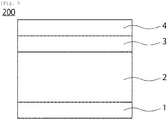
- FIG. 5 is a schematic cross-sectional view of a solar cell 200.
- the solar cell 200 of FIG. 5 includes the first transparent electrode 1, the photoelectric conversion layer 2, an n-type layer 3, and a second transparent electrode 4.
- the stacked body in which the first transparent electrode 1 and the photoelectric conversion layer 2 are stacked on each other is the same as the stacked thin film 100 of the first embodiment.
- the photoelectric conversion layer 2 is disposed between the first transparent electrode 1 and the n-type layer 3.
- the n-type layer 3 is disposed between the photoelectric conversion layer 2 and the second transparent electrode 4.
- the photoelectric conversion layer 2 and the n-type layer 3 form a pn junction.
- the first transparent electrode 1 and the photoelectric conversion layer 2 are the same as those of the first embodiment, and the description of these elements will be omitted.
- an intermediate layer (not shown) may be disposed between the n-type layer 3 and the second transparent electrode 4.
- a solar cell having a photoelectric conversion layer with a narrower band gap than the photoelectric conversion layer 2 e.g. a Si solar cell
- the n-type layer 3 is an n-type semiconductor layer disposed on the photoelectric conversion layer 2. It is preferable that the n-type layer 3 be an oxide layer or a sulfide layer.
- the sulfide used for the n-type layer 3 is preferably one or more sulfides selected from, but not limited to, the group including Zn x In (2-2x) S (3-2x) , ZnS, and In x Ga (1-x) S.
- the range of x is 0 ⁇ x ⁇ 1, and the range of y is 0 ⁇ y ⁇ 2.
- the film thickness of the n-type layer 3 is typically 5 nm or more and 100 nm or less. If the n-type layer 3 has poor coverage, the n-type layer 3 having a thickness equal to or less than 5 nm may cause a leak current and degradation in quality. When the n-type layer 3 has good coverage, the film thickness is not limited to the above range. The n-type layer 4 having a thickness more than 100 nm may cause excessively higher resistance of the n-type layer 3 and the resulting degradation in quality, and lower transparency and the resulting current reduction due to a short circuit. Accordingly, the thickness of the n-type layer 3 is more preferably 10 nm or more and 50 nm or less.
- the surface roughness of the n-type layer 3 is preferably equal to or less than 5 nm.
- the high-quality n-type layer 3 enables the operation of a solar cell having a thickness of approximately 200 nm.
- the conduction band offset ( ⁇ E Ecp - Ecn), which is a difference between the level (Ecp (eV)) of the conduction band minimum (CBM) of the photoelectric conversion layer 2 and the level (Ecn (eV)) of the CBM of the n-type layer 3, is preferably -0.2 eV or more and 0.6 eV or less (-0.2 eV ⁇ ⁇ E ⁇ +0.6 eV). If the conduction band offset is more than 0, the conduction band of the pn junction interface becomes discontinuous, which causes spikes. If the conduction band offset is less than 0, the conduction band of the pn junction interface becomes discontinuous, which causes cliffs.
- the conduction band offset is more preferably 0.0 eV or more and 0.4 eV or less (0.0 eV ⁇ ⁇ E ⁇ +0.4 eV). If the conduction takes place based on a gap level; however, this may not be applied.
- the level of a CBM can be estimated using the following method.
- the valence band maximum (VBM) is measured by photoemission spectroscopy, which is an evaluation method for an electron occupancy level, and then the band gap of an object material is estimated to determine the CBM.
- inverse photoelectron spectroscopy which directly uses a reverse process of photoemission, be used for evaluating a CBM. Specifically, performing low-energy etching and repeated photoemission spectroscopy and inverse photoelectron spectroscopy on the surface of a solar cell can evaluate the state of electrons in a pn junction interface.
- the second transparent electrode 4 it is preferable that one of the transparent electrically-conductive oxide films listed above for the first transparent electrode 3 or the stacked body including the transparent electrically-conductive oxide film be used.
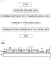
- FIG. 6 is a flowchart showing the method for manufacturing the solar cell 200.
- the method for manufacturing the solar cell 200 includes: a step (S00) for reducing the pressure in the chamber where the first transparent electrode 1 is disposed to 5 ⁇ 10 -3 [Pa] or less, a step (S01) for forming the photoelectric conversion layer 2 on the first transparent electrode 1 by sputtering using a target mainly composed of copper in an atmosphere at an oxygen partial pressure of 0.01 [Pa] or more and 10 [Pa] or less, a step (S02) for forming the n-type layer 3, and a step (S03) for forming the second transparent electrode 4.
- the step (S00) for pressure reduction and the step (S01) for formation of the photoelectric conversion layer 2 are the same as those in the first embodiment, and the description of these steps will be omitted.
- the n-type layer 3 is formed on the photoelectric conversion layer 2.
- the n-type layer 3 can be formed by sputtering using a target of the metal included in the n-type layer 3 at a room temperature in an oxidizing atmosphere or a sulfurizing atmosphere.
- the method for forming the n-type layer 3 is not limited to the above method. Examples of the method include chemical bath deposition (CBD), chemical vapor deposition (CVD), atomic layer deposition (ALD), coating method, electrodeposition, spraying, and vapor deposition.
- the second transparent electrode 4 is formed on the n-type layer 3.
- the second transparent electrode 4 is preferably formed by sputtering, for example.
- a semi-insulating film is disposed between the n-type layer 3 and the second transparent electrode 4 as an intermediate layer, for example, a ZnO film or the like is preferably formed by sputtering or the like after the formation of the n-type layer 3.
- the second transparent electrode 4 is then formed on the intermediate layer.
- Applying the method for manufacturing the stacked thin film 100 of the first embodiment to the second embodiment enables the manufacturing of a solar cell having excellent light transparency.
- Using light transparent films having excellent light transparency for the photoelectric conversion layer 2 and forming light transparent films for the other layers provide a solar cell having excellent light transparency.
- FIG. 7 is a schematic cross-sectional view of a part of a solar cell module 300.
- the solar cell module 300 of FIG. 7 includes a top cell 301 and a bottom cell 302.
- the solar cell module 300 may be a unijunction solar cell module 304 including the solar cell 200 of the embodiment without the bottom cell 302 (the top cell 301 of FIG. 7 ), as shown in the schematic cross-sectional view of FIG. 8 .
- the solar cell 200 of the second embodiment is used for the solar cell for the top cell 301. It is preferable that the top cell 301 and the bottom cell 302 be bonded to each other using an adhesive layer (not shown).
- the top cell 301 includes an extraction electrode 303 in electrical connection with a plurality of the solar cells 200.
- the solar cells 200 are electrically connected with each other.
- FIG. 7 the solar cells 200 connected with each other are included in a group of the top cells 301, and the solar cells 200 are electrically connected with the top cells 301.
- the embodiments shown in FIGS. 7 and 8 are examples in which a plurality of the solar cells 200 is modularized. As one of unshown examples, there is an embodiment in which solar cells not subjected to scribing such as the solar cell 200 of FIG. 5 are electrically connected in series or in parallel.
- the top cell 301 has a scribed cross-section.
- P1 of the first transparent electrode 1 is a first scribed cross-section.
- P2 of the photoelectric conversion layer 2 and the n-type layer 3 is a second scribed cross-section.
- P3 of the photoelectric conversion layer 2, the n-type layer 3, and the second transparent electrode 4 is a third scribed cross-section. Scribing separates the layers from each other and divides the solar cell 200 into small regions, which are electrically connected with each other.
- the top cell 301 has a light incident side on the second transparent electrode 4 side (the n-type layer 3 side); however, the top cell 301 may be turned over to have a light incident side on the first transparent electrode 1 side (the photoelectric conversion layer 2 side).
- the extraction electrode 303 is aluminum or copper wiring, for example, and connected with a terminal that extracts electricity generated by the solar cell 200.
- the bottom cell 302 is a solar cell including a photoelectric conversion layer having a narrower band gap than the photoelectric conversion layer 2 of the top cell.
- the bottom cell includes a solar cell having a Si photoelectric conversion layer. Since the top cell 301 includes the photoelectric conversion layer 2 having high transparency to light at a wavelength of 700 nm or more and 1000 nm or less, the top cell 301 combined with the bottom cell 302 that absorbs light at a wavelength in this range for power generation enables high efficient power generation of the solar cell module 300 as a whole. Electric power generated by the solar cell module 300 is transmitted through a power transmission line to be consumed or stored in a storage battery.
- FIG. 9 is a flowchart showing the method for manufacturing the solar cell module 300.
- the method for manufacturing the solar cell module 300 includes: a step (S10) for forming the first transparent electrode 1 on the substrate 10, a step (S11) for scribing the first transparent electrode 1 (a first scribing), the step (S00) for reducing the pressure in the chamber where the first transparent electrode 1 is disposed to a pressure of 5 ⁇ 10 -3 [Pa] or less, the step (S01) for forming the photoelectric conversion layer 2 on the first transparent electrode 1 by sputtering using a target mainly composed of copper in an atmosphere at an oxygen partial pressure of 0.01 [Pa] or more and 10 [Pa] or less, the step (S02) for forming the n-type layer 3, a step (S12) for scribing the photoelectric conversion layer 2 and the n-type layer 3 (a second scribing), the step (S03) for forming the
- the first transparent electrode 1 is formed on the substrate 10 by sputtering, for example.
- the first transparent electrode 1 is formed by repeated deposition with different targets.
- the first transparent electrode 1 is divided into several parts to expose the scribed cross-section P1. It is preferable that the cross-section P1 be exposed through laser, mechanical, or chemical processing.
- the step (S00) for reducing the pressure in the chamber where the first transparent electrode 1 is disposed to 5 ⁇ 10 -3 [Pa] or less and the step (S01) for forming the photoelectric conversion layer 2 on the first transparent electrode 1 by sputtering using a target mainly composed of copper in an atmosphere at an oxygen partial pressure of 0.01 [Pa] or more and 10 [Pa] or less are the same as those in the first embodiment.
- the photoelectric conversion layer 2 is deposited also on the gap between two first transparent electrodes 1 (the gap between the cross-sections P1) made as a result of scribing.
- the step (S02) for forming the n-type layer 3 is the same as that in the first embodiment.
- the photoelectric conversion layer 2 and the n-type layer 3 are cut in the stacked direction of the photoelectric conversion layer 2 and the n-type layer 3 to expose the scribed cross-section P2. It is preferable that the cross-section P2 be exposed through laser, mechanical, or chemical processing.
- the second transparent electrode 4 is formed on the n-type layer 3.
- the second transparent electrode 4 is formed by repeated deposition with different targets.
- the second transparent electrode is deposited also on the gap between two photoelectric conversion layers 2 and n-type layers 3 (the gap between the cross-sections P2) made as a result of scribing.
- the photoelectric conversion layer 2, the n-type layer 3, and the second transparent electrode 4 are cut in the stacked direction of the photoelectric conversion layer 2 and the n-type layer 3 to expose the scribed cross-section P3. It is preferable that the cross-section P3 be exposed through laser, mechanical, or chemical processing.
- the third scribing provides a plurality of the solar cells 200 electrically connected with each other.
- step (S14) for forming the extraction electrode 303 metal wiring is formed on the first transparent electrode 1, for example. Forming the extraction electrode 303 completes the top cell 301. After this step, it is preferable that, for example, the solar cell 200 be protected by filling gaps with resin.
- the step (S15) for bonding the top cell 301 and the bottom cell 302 that have been obtained in the previous steps completes the manufacturing of the multi-junction solar cell module 300. It is preferable that the top cell 301 and the bottom cell 302 be bonded together by applying an adhesive layer between the substrate 10 and the bottom cell 302, for example.
- top cell 301 has interference fringes
- bonding the top cell 301 and the bottom cell 302 together substantially improves the transparency of the top cell 301, which is preferable in view of efficient power generation in the bottom cell 302.
- a fifth embodiment relates to a solar power generation system.
- the solar cell module of the fourth embodiment can be used as a generator for generating power in the solar power generation system of the fifth embodiment.
- the solar power generation system according to the present embodiment performs power generation using the solar cell module, and specifically includes a solar cell module that generates power, a unit that converts the generated electricity into power, and a storage unit for storing the generated electricity or a load for consuming the generated electricity.
- FIG. 10 shows the structure of a solar power generation system 400 of the present embodiment.
- the solar power generation system of FIG. 10 includes a solar cell module 401 (300), a converter 402, a storage battery 403, and a load 404.
- the storage battery 403 or the load 404 may be omitted.
- the load 404 may be configured to be able to use the electric energy stored in the storage battery 403.
- the converter 402 is a device, such as a DC to DC converter, a DC to AC converter, or an AC to AC converter, which includes a circuit or element for performing power conversion such as voltage transformation or DC to AC conversion.
- the configuration of the converter 402 may be any suitable configuration depending on the configuration of the generated voltage, the storage battery 403, or the load 404.
- the solar battery cells included in the submodule 301, which received light, in the solar cell module 300 generates electric power, and the electric power is converted by the converter 402 to be stored in the storage battery 403 or consumed in the load 404.
- the solar cell module 401 includes a sunlight tracking driving device for always directing the solar cell module 401 toward the sun or a light collector for collecting sunlight, or adds a device for further improving the power generation efficiency.
- the solar power generation system 400 is used in real estate including residences, commercial facilities or factories, or used for movable property such as an aircraft, an electronic device, and the like.
- the solar cells having excellent conversion efficiency of the present embodiment in the solar cell module it is expected to provide the solar cell module which is lightweight and achieves an increased amount of power generation.
- FIG. 11 is a schematic view of a vehicle 500.
- the vehicle 500 of FIG. 11 includes a vehicle body 501, a solar cell module 502, a power converter 503, a storage battery 504, a motor 505, and a tire (wheel) 506.
- Electric power generated by the solar cell module 502 provided on the top of the vehicle body 501 is converted by the power converter 503 and stored in the storage battery 504 or consumed due to the load of the motor 505 or the like.
- the vehicle 500 can be moved by using electric power provided from the solar cell module 502 or the storage battery 504 and operating the motor 505 to rotate the tire (wheel) 506.
- the solar cell module 501 may be a first solar cell module including the solar cell 200 of the second embodiment as well as a multi-junction solar cell module.
- the solar cell module 501 having transparency can advantageously be used on the side of the vehicle body 501 as a power-generating window as well as on the top of the vehicle body 501.
- the stacked thin film 100, the solar cell 200 including the stacked thin film 100, and the solar cell module 300 including the stacked thin film 100 will now be discussed showing some examples.
- an ITO transparent electrically-conductive film is deposited on a white sheet glass substrate and a Sb-doped SnO 2 transparent electrically-conductive film is deposited on the ITO transparent electrically-conductive film, as a backside first transparent electrode.
- the pressure in the chamber housing the transparent member including the first transparent electrode is reduced to 1 ⁇ 10 -3 [Pa] or less.
- a cuprous oxide compound film is formed as a photoelectric conversion layer by RF magnetron sputtering through heating at 500°C in an atmosphere of oxygen and argon gas. At this time, the oxygen partial pressure is 0.035 [Pa], the deposition rate is 0.04 [ ⁇ m/min], and the film thickness is 2 ⁇ m.
- n-type Zn 0.8 Ge 0.2 O x is deposited on the p- cuprous oxide layer, and then an AZO transparent electrically-conductive film is deposited as a frontside second transparent electrode.
- the frontside second transparent electrode is deposited at a room temperature in order to prevent the oxidation of cuprous oxide; however, using AZO provides a low-resistant film even by the deposition at a room temperature, for example.
- the AZO target has 2wt% of Al 2 O 3 with respect to ZnO.
- MgF 2 is deposited on the second transparent electrode as an anti-reflective film.
- an ITO transparent electrically-conductive film is deposited on a white sheet glass substrate and a Sb-doped SnO 2 transparent electrically-conductive film is deposited on the ITO transparent electrically-conductive film, as a backside first transparent electrode.
- the pressure in the chamber housing the transparent member including the first transparent electrode is reduced to 1 ⁇ 10 -3 [Pa] or less.
- a cuprous oxide compound film is formed as a photoelectric conversion layer by DC magnetron sputtering at 450°C in an atmosphere of oxygen and argon gas. At this time, the oxygen partial pressure is 0.15 [Pa], the deposition rate is 0.2 [pm/min], and the film thickness of the photoelectric conversion layer is 2 ⁇ m.
- n-type Zn 0.8 Ge 0.2 O x is deposited on the p-cuprous oxide layer.
- An AZO transparent electrically-conductive film is then deposited as a frontside second transparent electrode.
- the AZO target has 2wt% of Al 2 O 3 with respect to ZnO.
- MgF 2 is deposited on the second transparent electrode as an anti-reflective film.
- the solar cell is made under the same conditions as in Example 1 except that the deposition rate is 0.032 [ ⁇ m/min], the oxygen partial pressure is 0.0166 [Pa], and the film thickness is 2 ⁇ m.
- the solar cell is made under the same conditions as in Example 1 except that the deposition rate is 0.017 [pm/min], the oxygen partial pressure is 0.025 [Pa], and the film thickness is 2 ⁇ m.
- the solar cell is made under the same conditions as in Example 1 except that the Cu 2 O film is formed to have a thickness of 3 ⁇ m by sputtering at 490°C.
- the solar cell is made under the same conditions as in Example 1 except that the Cu 2 O film is formed to have a thickness of 500 nm by sputtering at 350°C.
- the solar cell is made under the same conditions as in Example 1 except that the Cu 2 O film is formed to have a thickness of 1.5 ⁇ m by sputtering at 300°C.
- an ITO transparent electrically-conductive film is deposited on a white sheet glass substrate and a Sb-doped SnO 2 transparent electrically-conductive film is deposited on the ITO transparent electrically-conductive film, as a backside first transparent electrode.
- the pressure in the chamber housing the transparent member including the first transparent electrode is reduced to 1 ⁇ 10 -3 [Pa] or less.
- a cuprous oxide compound film is formed as a photoelectric conversion layer by RF magnetron sputtering through heating at 500°C in an atmosphere of oxygen and argon gas. At this time, the oxygen partial pressure is 0.009 [Pa] and the deposition rate is 0.04 [ ⁇ m/min].
- n-type Zn 0.8 Ge 0.2 O x is deposited on the p-cuprous oxide layer.
- An AZO transparent electrically-conductive film is then deposited as a frontside second transparent electrode.
- the frontside second transparent electrode is deposited at a room temperature in order to prevent the oxidation of cuprous oxide; however, using AZO provides a low-resistant film even by the deposition at a room temperature, for example.
- the AZO target has 2wt% of Al 2 O 3 with respect to ZnO.
- MgF 2 is deposited on the second transparent electrode as an anti-reflective film.
- the solar cell is made under the same conditions as in Example 1 except that the deposition rate is 0.01 [pm/min], the oxygen partial pressure is 0.034 [Pa], and the film thickness is 580 nm.
- the solar cell is made under the same conditions as in Example 1 except that the deposition rate is 0.01 [ ⁇ m/min], the oxygen partial pressure is 0.034 [Pa], and the film thickness is 2 ⁇ m.
- the solar cell is made under the same conditions as in Example 1 except that the deposition rate is 0.017 [ ⁇ m/min], the oxygen partial pressure is 0.034 [Pa], and the film thickness is 500 nm.
- the solar cell is made under the same conditions as in Example 1 except that the deposition rate is 0.0325 [ ⁇ m/min], the oxygen partial pressure is 0.0147 [Pa], and the film thickness is 650 nm.
- the solar cell is made under the same conditions as in Example 1 except that the deposition rate is 0.0333 [ ⁇ m/min] and the oxygen partial pressure is 0.0035 [Pa].
- the solar cell is made under the same conditions as in Example 1 except that the Cu 2 O film is formed by sputtering at room temperature.
- the solar cell is made under the same conditions as in Example 1 except that the Cu 2 O film is formed by sputtering at 200°C.
- the Cu 2 O film was formed, by sputtering at 500°C, on the ITO film without an Sb-doped SnO 2 transparent electrically-conductive film, which resulted in the deformation of the substrate. The film formation of the Cu 2 O film was then stopped.
- the light transparency of the obtained solar cell was evaluated at a wavelength of 700 nm.
- the solar cell was evaluated as level A.
- the solar cell was evaluated as level B.
- the solar cell was evaluated as level C.
- the conversion efficiency of the obtained solar cell was also determined.
- the relative value to Comparative Example 1 was more than 1, the solar cell was evaluated as level A.
- the relative value was 0.6 or more and less than 1, the solar cell was evaluated as level B.
- the relative value was 0.1 or more and less than 0.6, the solar cell was evaluated as level C.
- the solar cell When the average grain size of the Cu 2 O crystals in the photoelectric conversion layer (the reference area: D10 to D90) was 1000 nm or more, the solar cell was evaluated as level A. When the average grain size was 500 nm or more and less than 1000 nm, the solar cell was evaluated as level B. When the average grain size was less than 500 nm, the solar cell was evaluated as level C. When the ratio of the average grain size of the crystals to the thickness of the photoelectric conversion layer was 0.5 or more, the solar cell was evaluated as level A. The ratio was 0.25 or more and less than 0.5, the solar cell was evaluated as level B. When the ratio was less than 0.25, the solar cell was evaluated as level C. The results are shown in Table 1.
- Both the solar cells of Examples 1 and 2 have a light transparency equal to or more than 60%, which is excellent in a light transparency. Since these solar cells have high transparency to light at a wavelength of 700 nm, they can advantageously be applied to multi-junction solar cells (modules) in which they are connected with Si solar cells in tandem junctions.
- the high light transparencies of the solar cells of Examples 1 and 2 demonstrate that the cuprous oxide layers in the photoelectric conversion layers have excellent crystallinity. The excellent crystallinity is reflected on the conversion efficiencies of the solar cells of Examples, both of which are better than that of Comparative Example.
- the solar cells of Examples 3 and 4 in which the Cu 2 O films contain small amounts of Cu and CuO, have lower transparencies than those of Examples 1 and 2, while their conversion efficiencies are good.
- a tandem solar cell including a Si solar cell as the bottom cell for example, a solar cell having high transparency such as those of Examples 1 and 2 is preferable because light at a relatively long wavelength should reach the bottom cell of the tandem solar cell.
- the oxygen partial pressures of Examples 1 and 2 are in the range of 0.5 ⁇ d [Pa] or more and 1.5 ⁇ d [Pa] or less.
- a solar cell having an oxygen partial pressure of 0.24 ⁇ d [Pa] or more and 2.4 ⁇ d [Pa] or less, or 0.01 [Pa] or more and 4.8 [Pa] or less will have light transparency and conversion efficiency although such a solar cell is inferior to the solar cells of Examples 1, 2, 3, and 4, for example. Even if the deposition rate is in the preferable range, too high oxygen partial pressure tends to cause CuO generation and too low oxygen partial pressure tends to cause Cu generation. Therefore, it is important to form a cuprous oxide layer within the above range.
- FIG. 12 is a graph showing measurement results obtained through X-ray diffraction (XRD) on the stacked thin film including the photoelectric conversion layer and the transparent electrode of Example 5.
- XRD X-ray diffraction
- no heterogeneous substances such as CuO are determined, which means the stacked thin film is a substantially homogeneous Cu 2 O film.
- the half value width of the Cu 2 O (111) peak between 36° to 37° is very narrow, the high crystallinity of the photoelectric conversion layer of the embodiment is confirmed.
- some elements are described only by their element symbols.
Landscapes
- Chemical & Material Sciences (AREA)
- Engineering & Computer Science (AREA)
- Organic Chemistry (AREA)
- Materials Engineering (AREA)
- Mechanical Engineering (AREA)
- Metallurgy (AREA)
- Chemical Kinetics & Catalysis (AREA)
- Photovoltaic Devices (AREA)
- Life Sciences & Earth Sciences (AREA)
- Sustainable Development (AREA)
- Physical Vapour Deposition (AREA)
- Sustainable Energy (AREA)
- Manufacturing & Machinery (AREA)
Abstract
Description
- Embodiments described herein relate generally to a method for manufacturing a stacked thin film, a method for manufacturing a solar cell, and a method for manufacturing a solar cell module.
- Multi-junction (tandem) solar cells are known as high-efficiency solar cells. Tandem solar cells are more efficient than unijunction solar cells because tandem solar cells include cells having higher spectral sensitivity for each wavelength range. One of prospective materials for the top cells of tandem solar cells is a cuprous oxide compound, which is inexpensive and has a wide band gap. Some conventional cuprous oxide solar cells made of oxidized copper foils have been reported to achieve an efficiency of approximately 8%; however, this efficiency is lower than the theoretical efficiency limit. This is considered to be poor pn junctions caused by heterogeneous substances such as copper oxide that have not been removed sufficiently by etching from the uppermost surfaces after the oxidization of copper foils, or residual elements of etching solution. Moreover, in the conventional methods,
it is necessary that an oxidized foil having a thickness of approximately 0.1 mm be polished to have a thickness of approximately 20 µm, and it is difficult to increase area of solar cell. - There is another method in which a thin film is manufactured through reaction in a liquid phase; however, the efficiency is approximately 4% at the highest. The main cause is that the impurities in the solution as well as heterogeneous substances are absorbed into the film and become the centers of the recombination of photoexcitation carriers. Such a thin film absorbs light at a wavelength equal to or more than 600 nm, which is not to be absorbed originally. Therefore, this thin film cannot be used for the top cell of a tandem solar cell. Sputtering is generally known as a method for manufacturing a thin film containing fewer impurities. Thin films manufactured in this method, however, have been reported to have a conversion efficiency equal to or less than 1%. This is because even if no impurity contamination occurs, heterogeneous substances such as copper and cupric oxide are easily generated, which makes it difficult to manufacture high-quality cuprous oxide layers.
- [NPL 1] Tadatsugu Minami et al. Applied Physics Express 9, 052301(2016)
- Problems to be solved by the present invention provide a method for manufacturing a stacked thin film with excellent transparency, a method for manufacturing a solar cell, and a method for manufacturing a solar cell module.
- A method for manufacturing a stacked thin film of an embodiment, includes forming a photoelectric conversion layer on a first transparent electrode by sputtering using a target mainly composed of copper in an oxygen containing atmosphere. An oxygen partial pressure of the sputtering is in a range of 0.01 [Pa] or more and 4.8 [Pa] or less, and 0.24 × d [Pa] or more and 2.4 × d [Pa] or less when a deposition rate is d [µm/min], in formation of the photoelectric conversion layer. A sputtering temperature is 300°C or more and 600°C or less, in formation of the photoelectric conversion layer.
-
- [
Fig. 1 ] A schematic cross-sectional view of a stacked thin film according to an embodiment. - [
Fig. 2 ] A flowchart showing a method for manufacturing a stacked thin film according to an embodiment - [
Fig. 3 ] A graph showing a relationship between an oxygen partial pressure and a deposition rate in an embodiment; - [
Fig. 4 ] A schematic cross-sectional view of a stacked thin film according to an embodiment; - [
Fig. 5 ] A schematic cross-sectional view of a solar cell according to an embodiment; - [
Fig. 6 ] A flowchart showing a method for manufacturing a solar cell according to an embodiment; - [
Fig. 7 ] A schematic cross-sectional view of a solar cell module according to an embodiment; - [Fig. 8 A schematic cross-sectional view of a solar cell module according to an embodiment;
- [
Fig. 9 ] A flowchart showing a solar cell module according to an embodiment; - [
Fig. 10 ] A schematic view of a solar power generation system according to an embodiment; - [
Fig. 11 ] A schematic view of a vehicle according to an embodiment; and - [
Fig. 12 ] A graph showing measurement results of Example 5 obtained through X-ray diffraction (XRD). - A first embodiment relates to a stacked thin film and a method for manufacturing a stacked thin film.
FIG. 1 is a schematic cross-sectional view of a stacked thin film 100. A stacked thin film 100 ofFIG. 1 includes a firsttransparent electrode 1 and aphotoelectric conversion layer 2 formed on the firsttransparent electrode 1. - The first
transparent electrode 1 constitutes a stacked structure together with thephotoelectric conversion layer 2. InFIG. 1 , the firsttransparent electrode 1 is in direct contact with thephotoelectric conversion layer 2. The main surface of the firsttransparent electrode 1 faces the main surface of thephotoelectric conversion layer 2, and these two main surfaces share an interface. It is preferable that the entire surface of thephotoelectric conversion layer 2, which faces the firsttransparent electrode 1, be in direct contact with the firsttransparent electrode 1. The firsttransparent electrode 1 is a p-type electrode in direct contact with thephotoelectric conversion layer 2, which is also p-type. It is preferable that the firsttransparent electrode 1 have a thickness of 100 nm or more and 1000 nm or less, for example. - It is preferable that the first
transparent electrode 1 include a transparent electrically-conductive oxide film. Materials for the transparent electrically-conductive oxide film include, but not limited to, indium tin oxide (ITO), Al-doped zinc oxide (AZO), boron-doped zinc oxide (BZO), gallium-doped zinc oxide (GZO), fluorine-doped tin oxide (FTO), antimony-doped tin oxide (ATO), titanium-doped indium oxide (ITiO), indium zinc oxide (IZO), indium gallium zinc oxide (IGZO), Ta-doped tin oxide (SnO2:Ta), Nb-doped tin oxide (SnO2:Nb), W-doped tin oxide (SnO2:W), Mo-doped tin oxide (SnO2:Mo), F-doped tin oxide (SnO2:F), and hydrogen-doped indium oxide (IOH). Such a transparent electrically-conductive oxide film may be a stacked film including a plurality of films and include a tin oxide film other than the above oxides. Dopants for films such as the tin oxide film include, but not limited to, one or more substances selected from the group including In, Si, Ge, Ti, Cu, Sb, Nb, F, Ta, W, Mo, Br, I, and Cl. It is preferable that thephotoelectric conversion layer 2 be in direct contact with the transparent electrically-conductive oxide film included in the firsttransparent electrode 1. - It is preferable that the first
transparent electrode 1 have a stacked structure in which an indium tin oxide film and a doped tin oxide film are stacked on each other. Specifically, it is preferable that the firsttransparent electrode 1 have one or more stacked structures selected from the group including a stacked film of an indium tin oxide film and an antimony-doped tin oxide film, a stacked film of an indium tin oxide film and a fluorine-doped tin oxide film, a stacked film of an indium tin oxide film and a Ta-doped tin oxide film, and a stacked film of an indium tin oxide film and a Nb-doped tin oxide film. When the firsttransparent electrode 1 includes a doped tin oxide film, it is preferable that the doped tin oxide film be in direct contact with thephotoelectric conversion layer 2. - The first
transparent electrode 1 may include a metal film having a thickness equal to or less than 10 nm. The metal film includes, but not limited to, one or more films selected from the group including Mo, Au, Cu, Ag, Al, Ta, Pt, Ru, and W. The firsttransparent electrode 1 may be an electrode including metal in a dot form, a line form, or a mesh form on the top or bottom of the transparent electrically-conductive oxide film. In this case, the metal in a dot form, a line form, or a mesh form is disposed between the transparent electrically-conductive oxide film and thephotoelectric conversion layer 32. It is preferable that the metal in a dot form, a line form, or a mesh form have an aperture ratio equal to or more than 50% with respect to the transparent electrically-conductive oxide film. The metal in a dot form, a line form, or a mesh form includes, but not limited to, Mo, Au, Cu, Ag, Al, Ta, Pt, Ru, and W. Because providing the metal in a dot form, a line form, or a mesh form ensures transparency, the metal film may have any thickness. - In view of improving the crystallinity of the
photoelectric conversion layer 2, it is preferable that the surface of the firsttransparent electrode 1 on which thephotoelectric conversion layer 2 will be formed be a thin film of a metallic oxide mainly composed of Sn (a transparent electrically-conductive oxide film). It is preferable that Sn account for 90 atom% or more in the metal of the metallic oxide mainly composed of Sn. The metallic oxide thin film mainly composed of Sn may contain one or more metals (metallic oxides) selected from the group consisting of Zn, Al, Ga, In, Si, Ge, Ti, Cu, Sb, Nb, F, and Ta other than Sn. If thephotoelectric conversion layer 2 is formed directly on a metallic oxide mainly composed of In (e.g. ITO), the stacked boy of the ITO film and the substrate is easily deformed due to a high temperature. Therefore, an ITO film is not suitable for the direct formation of a Cu2O film thereon. - The
photoelectric conversion layer 2 is a p-type compound semiconductor layer mainly composed of cuprous oxide. Cuprous oxide is represented by Cu2O and is an oxide semiconductor. Cuprous oxide is non-doped or doped cuprous oxide. Thephotoelectric conversion layer 2 has a thickness of 500 nm or more and 10 µm or less, for example. The thickness of thephotoelectric conversion layer 2 is preferably 1000 nm or more and 5 µm or less, and more preferably 1500 nm or more and 3 µm or less. The thickness of thephotoelectric conversion layer 2 can be determined through cross-section observation, for example. - It is preferable that the
photoelectric conversion layer 2 have many large cuprous oxide crystals and contribute to excellent conversion efficiency and light transparency of a solar cell including the stacked thin film 100. The stacked thin film 100 manufactured by the method according to an embodiment of the present disclosure will have large cuprous oxide crystals and contribute to the improved conversion efficiency and light transparency. It is preferable that thephotoelectric conversion layer 2 contain cuprous oxide at 95wt% or more. It is preferable that thephotoelectric conversion layer 2 contain cuprous oxide at 98wt% or more. In other words, it is preferable that thephotoelectric conversion layer 2 contain almost no (substantially little) heterogeneous substances such as CuO and Cu. Thephotoelectric conversion layer 2 containing almost no heterogeneous substances such as CuO and Cu and being a substantially homogeneous Cu2O thin film has very high light transparency, which is preferable. A photo luminescence (PL) method can be used for determining whether thephotoelectric conversion layer 2 is a substantially homogeneous Cu2O thin film or not. - It is preferable that the
photoelectric conversion layer 2 contain Cu of 60.0 atom% or more and 67.0 atom% or less and O (oxygen) of 32.5 atom% or more and 34.0 atom% or less. Thephotoelectric conversion layer 2 may contain an element selected from the group including metals other than Cu, dopants, and impurities, except Cu and O (oxygen). Thephotoelectric conversion layer 2 may contain a metal other than Cu as an oxide and be a complex oxide. The metals contained in thephotoelectric conversion layer 2 include one or more metals selected from the group including Sn, Sb, Ag, Li, Na, K, Cs, Rb, Al, Ga, In, Zn, Mg, and Ca, in addition to Cu. When thephotoelectric conversion layer 2 contains one or more metals selected from the group including Ag, Li, Na, K, Cs, Rb, Al, Ga, In, Zn, Mg, Ta, and Ca, in addition to Cu; the band gap of thephotoelectric conversion layer 2 can be adjusted. Thephotoelectric conversion layer 2 may have a p+ region containing one or more p-type dopants selected from Si, Ge, and N at a high content on the side adjacent to the firsttransparent electrode 1. - It is preferable that the band gap of the
photoelectric conversion layer 2 be 2.0 eV or more and 2.2 eV or less. In a multi-junction solar cell including a solar cell having a light absorbing layer of Si as the bottom cell and a solar cell having a thin film of this embodiment as the top cell, the band gap in this range will enable both the top cell and the bottom cell to efficiently use solar energy. The composition of thephotoelectric conversion layer 2 can be represented by CuaMbOc. M represents one or more elements selected from the group including Si, Ge, N, Sn, Sb, Ag, Li, Na, K, Cs, Rb, Al, Ga, In, Zn, Mg, Ta, and Ca. It is preferable that the ranges of a, b, and c be 1.80 ≤ a ≤ 2.01, 0.00 ≤ b ≤ 0.20, and 0.98 ≤ c ≤ 1.02, respectively. The above composition ratio of thephotoelectric conversion layer 2 is the composition ratio of the entirephotoelectric conversion layer 2. In addition, it is preferable that the above compound composition ratio of thephotoelectric conversion layer 2 be met in the entirephotoelectric conversion layer 2. Thephotoelectric conversion layer 2 may contain additive(s) other than the above substances. - A method for manufacturing the stacked thin film 100 will now be described.
FIG. 2 is a flowchart showing the method for manufacturing the stacked thin film 100. The method for manufacturing the stacked thin film 100 includes a step (S01) for forming thephotoelectric conversion layer 2 on the firsttransparent electrode 1 by sputtering using a target mainly composed of copper in an atmosphere at an oxygen partial pressure of 0.01 [Pa] or more and 10 [Pa] or less. Before the step (S01) for formation of thephotoelectric conversion layer 2, the method may optionally include a step (S00) for pressure reduction. - The target mainly composed of copper has a copper purity equal to or more than 99.99%. The copper purity is preferably equal to or more than 99.995%, more preferably equal to or more than 99.999%. The target having a high cupper purity provides the substantially homogeneous Cu2O
photoelectric conversion layer 2. When the target contains the element(s) to be contained in the photoelectric conversion layer 2 (e.g. Si), the cupper purity may be different. - The sputtering atmosphere is preferably an oxidizing atmosphere in which inert gas and oxygen gas are mixed. The sputtering atmosphere is more preferably an atmosphere of inert gas and oxygen gas. The inert gas is preferably nitrogen gas, argon gas, or mixed gas of nitrogen gas and argon gas.
- Sputtering is performed on a base substrate in which the first
transparent electrode 1 is formed on asubstrate 10 such as a glass substrate, for example.FIG. 3 is a schematic cross-sectional view of a stacked thin film 100 including thesubstrate 10. Sputtering is performed on the firsttransparent electrode 1 so that thephotoelectric conversion layer 2 is deposited on the firsttransparent electrode 1. Before performing sputtering, it is preferable that the step (S00) be taken for reducing the pressure in the chamber where the firsttransparent electrode 1 is disposed to 5.0 × 10⁻³ [Pa] or less. The step (S00) for pressure reduction may be taken in a chamber for sputtering or a subchamber for sputtering. In the step for pressure reduction, different from the step for sputtering, oxygen is not introduced. Thesubstrate 10 can be used for a substrate for a solar cell including the thin film 100. The firsttransparent electrode 1 is formed on thesubstrate 10 by e.g. sputtering. It is preferable that thesubstrate 10 be made of glass such as white sheet glass, soda-lime glass, chemically strengthened glass, and quartz glass. Thesubstrate 10 may be made of an organic material such as acryl, polycarbonate, and polyimide. - The total pressure in the chamber during sputtering is typically 0.1 [Pa] or more and 10 [Pa] or less. Sputtering is performed in an atmosphere at an oxygen partial pressure of 0.01 [Pa] or more and 10 [Pa] or less (the first condition). Sputtering in this oxygen partial pressure range enables the deposition of substantially homogeneous cuprous oxide on the first
transparent electrode 1. When the oxygen partial pressure is too high, copper is oxidized too much and CuO is generated in addition to cuprous oxide. When the oxygen partial pressure is too low, copper is not oxidized sufficiently and part of the Cu is deposited in the form of metal. Heterogeneous substances such as CuO and Cu deposited on the firsttransparent electrode 1 will reduce the conversion efficiency of a solar cell including the stacked thin film 100 as well as the light transparency of the stacked thin film 100, which results in unsuitability for the top cell of a solar cell. Sputtering may be DC sputtering, RF sputtering, DC magnetron sputtering, RF magnetron sputtering, or ion beam sputtering. - When the oxygen partial pressure is in the range of 0.01 [Pa] or more and 4.8 [Pa] or less (the second condition) and the deposition rate is represented by d [µm/min] in the formation of the
photoelectric conversion layer 2, it is preferable, in view of the deposition of high-quality cuprous oxide, that the oxygen partial pressure is 0.5 × d [Pa] or more and 1.5 × d [Pa] or less (the third condition). The deposition rate can be determined based on the time during which sputtering is actually being performed. When sputtering is performed intermittently, the deposition rate is determined based on the time excluding the time during which sputtering is not being performed (film formation is not being performed).FIG. 4 is a graph showing a relationship between an oxygen partial pressure and a deposition rate in an embodiment of the present disclosure. The area enclosed by the thin lines inFIG. 4 is the range that meets the second and third conditions. It should be noted that the bold lines, the thin lines, and the broke lines overlap with each other at the oxygen partial pressures of 0.01 Pa and 4.8 Pa. Thephotoelectric conversion layer 2 having transparency can be formed within the area inside the bold lines. Thephotoelectric conversion layer 2 formed within the area inside the bold lines and inside the thin lines, however, has excellent crystallinity and very high transparency compared with thephotoelectric conversion layer 2 formed within the area inside the bold lines but outside the thin lines. Since too low deposition rate is not practical, it is preferable that the deposition rate be equal to or more than 0.02 µm/min (the fourth condition). The deposition rate is preferably equal to or less than 20 µm/min (the fifth condition). Because a high deposition rate in a large deposition area may impair the uniformity of thephotoelectric conversion layer 2, the deposition rate is more preferably equal to or less than 4 µm/min (the sixth condition). In view of practicability and film quality, it is preferable that the deposition rate be 0.02 [µm/min] or more and 4 [µm/min] or less (the seventh condition). In view of better practicability, it is preferable that the deposition rate be 1 [µm/min] or more and 4 [µm/min] or less (the eighth condition). The area over the area enclosed by the bold lines inFIG. 4 , in which the oxygen partial pressure is too high, is not preferable because a heterogeneous substance or CuO tends to increase in thephotoelectric conversion layer 2. The area under the area enclosed by the bold lines inFIG. 4 , in which the oxygen partial pressure is too low, is also not preferable because a heterogeneous substance or Cu tends to increase in thephotoelectric conversion layer 2. Adjusting the deposition rate and the oxygen partial pressure contributes to the deposition of higher quality cuprous oxide. - At a low oxygen partial pressure, the sputtering takes place at a low oxygen content. Under this condition, copper will not sufficiently be oxidized and the unoxidized copper will be deposited as a Cu phase (in a metal state). The increased amount of metal-state Cu will cause the
photoelectric conversion layer 2 to reflect light like a mirror. Thus, thephotoelectric conversion layer 2 should preferably have a decreased amount of metal-state Cu. For example, thephotoelectric conversion layer 2 formed within the area inside the bold lines and outside the thin lines and at a low oxygen partial pressure has metallic shine. Thephotoelectric conversion layer 2 formed within the area inside the bold lines and outside the thin lines and at a high oxygen partial pressure has a small amount of CuO and has slight cloudiness, which is visible. Thephotoelectric conversion layer 2 having slight cloudiness or metallic shine is still usable for a stand-alone solar cell. Such aphotoelectric conversion layer 2, however, does not have high transparency required by a multi-junction solar cell. If a solar cell including a photoelectric conversion layer with opacity and/or metallic shine is used for the top cell of a multi-junction solar cell, the power generation in the bottom cell will have substantial adverse effects. - The
photoelectric conversion layer 2 formed within the area inside the thin lines has no metallic shine and is transparent. Thus, thisphotoelectric conversion layer 2 achieves both high crystallinity and high transparency. - The
photoelectric conversion layer 2 with decreased crystallinity will have a gap level at a distance of 1.8 eV from the valence band maximum (VBM), for example, in the Cu2O film of thephotoelectric conversion layer 2. Specifically, the Cu2O film formed at an oxygen partial pressure of approximately 2.4 × d [Pa] contains a heterogeneous substance of CuO and will have a gap level. This may decrease the conversion efficiency as well as the transparency. The Cu2O film formed within the area inside the thin lines has high crystallinity and will have a very low gap level that has substantially no effect on the characteristics. Thus, this Cu2O film contributes to the high crystallinity and high conversion efficiency. If thephotoelectric conversion layer 2 having a gap level is used for a solar cell as the top cell of a multi-junction solar cell that has a solar cell including a light absorbing layer of Si as the bottom cell, the top cell will absorb most of the light at a wavelength to be absorbed by the bottom cell at the bottom. Thus, also in view of the multi-junction use, thephotoelectric conversion layer 2 should preferably have high crystallinity. In addition, since thephotoelectric conversion layer 2 having an increased amount of Cu and reflecting light is also not preferable in view of the multi-junction use, the oxygen partial pressure should preferably be within the area inside the thin lines. - In view of the deposition of cuprous oxide with higher-quality, the oxygen partial pressure of the third condition should more preferably be 0.55 × d [Pa] or more and 1.00 × d [Pa] or less. The more preferable range of the oxygen partial pressure is within the area shown by the broken lines in
Fig. 4 . The Cu2O film formed within the area inside the broken lines has higher crystallinity. The length of the Cu2O crystals in the direction of the film thickness is almost equal to the film thickness. Such a Cu2O film is substantially homogeneous. Thephotoelectric conversion layer 2 formed at an oxygen partial pressure of 0.50 × d [Pa] or more has substantially no metal-state Cu. Thus, increasing the oxygen partial pressure to 0.50 × d [Pa] or more has only limited effects on the decrease in the content of metal-state Cu. In thephotoelectric conversion layer 2 formed at an oxygen partial pressure of 0.55 × d [Pa] or more, the content of metal-state Cu is almost zero. Thephotoelectric conversion layer 2 formed at an oxygen partial pressure of 1.50 × d [Pa] or less has substantially no CuO. Thus, decreasing the oxygen partial pressure to 1.50 × d [Pa] or less has only limited effects on the decrease in the content of CuO. In this view, the oxygen partial pressure should more preferably be 0.55 × d [Pa] or more and 1.40 × d [Pa] or less. In thephotoelectric conversion layer 2 formed at an oxygen partial pressure of 1.00 × d [Pa] or less, the content of metal-state Cu is almost zero. When the Cu2O film is formed at an oxygen partial pressure within the area inside the broken lines, thephotoelectric conversion layer 2 will be a clear reddish-brown gem-like layer that has no metallic shine and high transparency, which is absorbed by the Cu2O. - When the film thickness of Cu2O is T, the average diameter of the Cu2O crystals in the direction of the film thickness (except minute Cu2O crystals having a diameter of 50 nm or less in the direction of the film thickness) should preferably be 0.7T or more and 1.0T or less in the
photoelectric conversion layer 2. Thephotoelectric conversion layer 2 containing such minute Cu2O crystals has many grain boundaries, which can probably decrease the conversion efficiency. The cross-section occupied by the minute Cu2O crystals having a diameter of 50 nm or less in the direction of the film thickness should preferably account for 10% or less of the cross-section of thephotoelectric conversion layer 2. - When the
photoelectric conversion layer 2 is a thin film having a film thickness of 100 nm or less, the CuO phase and the metal-state CU will have small effects on the decrease in the transparency. When thephotoelectric conversion layer 2 is a thick film having a film thickness of 500 nm or more, the CuO phase and the metal-state Cu will have large effects on the decrease in the transparency. Thus, the oxygen partial pressure in sputtering should more preferably be 0.55 × d [Pa] or more and 1.40 × d [Pa] or less. For forming a thickphotoelectric conversion layer 2 having a film thickness of 500 nm or more, the oxygen partial pressure in sputtering should more preferably be 0.55 × d [Pa] or more and 1.00 × d [Pa] or less. - As for sputtering conditions, the sputtering temperature (the temperature of a base substrate) is preferably 300°C or more and 600°C or less (the ninth condition), and the oxygen partial pressure is preferably in the range of 0.01 [Pa] or more and 4.8 [Pa] or less (the tenth condition) and 1.5 × 10+9 × e(-30000/sputtering temperature [K]) or more (the eleventh condition) (Here, e represents the Napierian number and an abbreviation of "exponential"). When all the ninth to eleventh conditions are met, the generation of heterogeneous substances such as CuO and Cu is further reduced. The temperature in the eleventh condition is not a Celsius degree but an absolute temperature in Kelvin. The range meeting these three conditions generally meets the conditions suitable for forming a CuO film. When the deposition rate is too low, a formed film may contain a large amount of CuO, which should carefully be avoided. It is preferable that the film formation be completed within approximately one hour. In the case of sputtering on a large area, in view of crystallization, the temperature in the ninth condition is preferably 300°C or more and 550°C or less, more preferably 350°C or more and 550°C or less, and more preferably 300°C or more and 500°C or less, and much more preferably 300°C or more and 450°C or less. It is preferable that the sputtering temperature be lower than the melting point of the
substrate 10. - Although the Cu2O film can be formed at a sputtering temperature of approximately 200°C or less, the grain size of the Cu2O crystals becomes small in this case, which is disadvantageous in terms of conversion efficiency. In a homogeneous Cu2O thin film having a thickness of 500 nm and a Cu2O crystal grain size of 100 nm or less, for example, small Cu2O crystals exist on top of each other in the film thickness direction and thus many grain boundaries exist in the thickness direction of the Cu2O film. When the
photoelectric conversion layer 2 has grain boundaries in the flow direction of electrons, recombination will easily occur and thus electric current and voltage will decrease, which will reduce the conversion efficiency. Sputtering is basically used for film formation at a low temperature (approximately 200°C or less). Sputtering is intended to provide a high-quality film through film formation using plasma while reducing heat damage due to a high temperature. In sputtering without intentional heating, the Cu2O crystals do not grow to the grain size approximately equal to the film thickness in the case of a Cu2O film having a thickness of hundreds nm or more. In the embodiment, however, the Cu2O crystals grow to the grain size approximately equal to the film thickness by sputtering while increasing the substrate temperature. When no grain boundary exists in the film thickness direction, the light transparency will improve. As a result, the Cu2O crystallinity improves and the conversion efficiency improves. The improved light transparency also increases the power generation in the lower solar cell, which eventually increases the total amount of electricity generated by the multi-junction solar cell. Electrons travel a longer distance in a thicker film, which makes recombination less negligible. In a thin film having a thickness of 100 nm or so, however, recombination will hardly occur even with a small grain size, and the light transparency will hardly decrease. In the embodiment, thephotoelectric conversion layer 2 is 500 nm at the thinnest. In the case of a film thickness of 1 µm or more, the grain size should be enlarged in order to achieve both high conversion efficiency and high light transparency. - In addition, when the
photoelectric conversion layer 2 is formed on a metallic oxide film mainly composed of Sn, Sn disperses into the Cu2O film during the film formation of the Cu2O film. This makes it easier to enlarge the grain size than in the case of sputtering on a glass substrate at the same temperature, and improves the crystallinity. By sputtering Cu2O on the metallic oxide film mainly composed of Sn at a higher temperature, the Cu2O film is formed to have Cu2O crystals with the grain size approximately equal to the film thickness, which could not be realized by sputtering at 200°C or so. As described above, this Cu2O film is a substantially homogeneous Cu2O film and thus has excellent crystallinity in the entire film and ideal conversion efficiency for an optically transparent solar cell. - It is also possible to form a Cu2O film having Cu2O crystals with the grain size approximately equal to the film thickness by oxidizing a Cu sheet at a high temperature. In this case, however, a transparent electrode is formed on the Cu2O film after the oxidization of the Cu sheet. If a transparent electrode is formed directly on the Cu2O film by sputtering, the Cu2O crystals will be damaged, which will reduce the power generation efficiency when being applied to a solar cell. In the stacked thin film of the embodiment, in which the
photoelectric conversion layer 2 is formed on thetransparent electrode 1, keeps the high quality of thephotoelectric conversion layer 2 after being applied to a solar cell. - Heating may be performed after sputtering. It is preferable that heating be performed on the stacked thin film 100 at a temperature equal to or more than a room temperature and equal to or less than the sputtering temperature for a predetermined period of time in the chamber.
- The stacked thin film 100 manufactured in this method will pass 50% or more of light at a wavelength of 700 nm or more and 1000 nm or less, which has excellent light transparency. The stacked thin film 100 having excellent light transparency can advantageously be used for the top cell of an optically transparent solar cell or a multi-junction solar cell in which power is efficiently generated also in the bottom cell.
- In this embodiment, the
photoelectric conversion layer 2 is not formed on a glass member but on the firsttransparent electrode 1. If thephotoelectric conversion layer 2 is formed on a glass member, the impurities in the glass will spread into thephotoelectric conversion layer 2. This may change the film forming conditions or deteriorate the film quality of thephotoelectric conversion layer 2 through the formation of impurity state. If thephotoelectric conversion layer 2 is formed on a metal film usable as an electrode, the stacked thin film 100 will be opaque. Since light transparency is a necessary characteristic in this embodiment, the stacked thin film having thephotoelectric conversion layer 2 on a metal film is impractical in view of light transparency. Glass partially exposed as a result of scribing is generally not a problem. This may not be applied if a cuprous oxide solar cell is used alone. - A second embodiment relates to a solar cell and a method for manufacturing a solar cell.
FIG. 5 is a schematic cross-sectional view of asolar cell 200. Thesolar cell 200 ofFIG. 5 includes the firsttransparent electrode 1, thephotoelectric conversion layer 2, an n-type layer 3, and a secondtransparent electrode 4. The stacked body in which the firsttransparent electrode 1 and thephotoelectric conversion layer 2 are stacked on each other is the same as the stacked thin film 100 of the first embodiment. Thephotoelectric conversion layer 2 is disposed between the firsttransparent electrode 1 and the n-type layer 3. The n-type layer 3 is disposed between thephotoelectric conversion layer 2 and the secondtransparent electrode 4. Thephotoelectric conversion layer 2 and the n-type layer 3 form a pn junction. The firsttransparent electrode 1 and thephotoelectric conversion layer 2 are the same as those of the first embodiment, and the description of these elements will be omitted. For example, an intermediate layer (not shown) may be disposed between the n-type layer 3 and the secondtransparent electrode 4. A solar cell having a photoelectric conversion layer with a narrower band gap than the photoelectric conversion layer 2 (e.g. a Si solar cell) can be stacked on thesolar cell 200 of the second embodiment to make a multi-junction solar cell. - The n-
type layer 3 is an n-type semiconductor layer disposed on thephotoelectric conversion layer 2. It is preferable that the n-type layer 3 be an oxide layer or a sulfide layer. The oxide used for the n-type layer 3 is preferably selected from, but not limited to, the group including Zn(1-x)AxOy (A = Si, Ge, Sn), Cu(2-x)MxOy (M = Mn, Mg, Ca, Zn, Sr, Ba, Al, Ga, In, Nb, Ta, lanthanoid), Cu2O:F, Cu2O:N, Cu2O: B, Cu2O: Cl, Cu2O: Br, Cu2O: I, and Al(2-x)GaxO3. The sulfide used for the n-type layer 3 is preferably one or more sulfides selected from, but not limited to, the group including ZnxIn(2-2x)S(3-2x), ZnS, and InxGa(1-x)S. The range of x is 0 ≤ x ≤ 1, and the range of y is 0 ≤ y ≤ 2. - The film thickness of the n-
type layer 3 is typically 5 nm or more and 100 nm or less. If the n-type layer 3 has poor coverage, the n-type layer 3 having a thickness equal to or less than 5 nm may cause a leak current and degradation in quality. When the n-type layer 3 has good coverage, the film thickness is not limited to the above range. The n-type layer 4 having a thickness more than 100 nm may cause excessively higher resistance of the n-type layer 3 and the resulting degradation in quality, and lower transparency and the resulting current reduction due to a short circuit. Accordingly, the thickness of the n-type layer 3 is more preferably 10 nm or more and 50 nm or less. In order to obtain a film having good coverage, the surface roughness of the n-type layer 3 is preferably equal to or less than 5 nm. The high-quality n-type layer 3 enables the operation of a solar cell having a thickness of approximately 200 nm. - The conduction band offset (ΔE = Ecp - Ecn), which is a difference between the level (Ecp (eV)) of the conduction band minimum (CBM) of the
photoelectric conversion layer 2 and the level (Ecn (eV)) of the CBM of the n-type layer 3, is preferably -0.2 eV or more and 0.6 eV or less (-0.2 eV ≤ ΔE ≤ +0.6 eV). If the conduction band offset is more than 0, the conduction band of the pn junction interface becomes discontinuous, which causes spikes. If the conduction band offset is less than 0, the conduction band of the pn junction interface becomes discontinuous, which causes cliffs. It is preferable that the spikes and cliffs are small because both the spikes and cliffs will become barriers for photogenerated electrons. Accordingly, the conduction band offset is more preferably 0.0 eV or more and 0.4 eV or less (0.0 eV ≤ ΔE ≤ +0.4 eV). If the conduction takes place based on a gap level; however, this may not be applied. The level of a CBM can be estimated using the following method. The valence band maximum (VBM) is measured by photoemission spectroscopy, which is an evaluation method for an electron occupancy level, and then the band gap of an object material is estimated to determine the CBM. However, because an actual pn junction interface, in which counter diffusion occurs and lattice defects, especially cation defects exist, is not an ideal interface, the band gap may probably vary. Therefore, it is preferable that inverse photoelectron spectroscopy, which directly uses a reverse process of photoemission, be used for evaluating a CBM. Specifically, performing low-energy etching and repeated photoemission spectroscopy and inverse photoelectron spectroscopy on the surface of a solar cell can evaluate the state of electrons in a pn junction interface. - For the second
transparent electrode 4, it is preferable that one of the transparent electrically-conductive oxide films listed above for the firsttransparent electrode 3 or the stacked body including the transparent electrically-conductive oxide film be used. - A method for manufacturing the
solar cell 200 will now be described.FIG. 6 is a flowchart showing the method for manufacturing thesolar cell 200. The method for manufacturing thesolar cell 200 includes: a step (S00) for reducing the pressure in the chamber where the firsttransparent electrode 1 is disposed to 5 × 10⁻³ [Pa] or less, a step (S01) for forming thephotoelectric conversion layer 2 on the firsttransparent electrode 1 by sputtering using a target mainly composed of copper in an atmosphere at an oxygen partial pressure of 0.01 [Pa] or more and 10 [Pa] or less, a step (S02) for forming the n-type layer 3, and a step (S03) for forming the secondtransparent electrode 4. The step (S00) for pressure reduction and the step (S01) for formation of thephotoelectric conversion layer 2 are the same as those in the first embodiment, and the description of these steps will be omitted. - In the step (S02) for forming the n-
type layer 3, the n-type layer 3 is formed on thephotoelectric conversion layer 2. The n-type layer 3 can be formed by sputtering using a target of the metal included in the n-type layer 3 at a room temperature in an oxidizing atmosphere or a sulfurizing atmosphere. The method for forming the n-type layer 3 is not limited to the above method. Examples of the method include chemical bath deposition (CBD), chemical vapor deposition (CVD), atomic layer deposition (ALD), coating method, electrodeposition, spraying, and vapor deposition. - In the step (S03) for forming the second
transparent electrode 4, the secondtransparent electrode 4 is formed on the n-type layer 3. The secondtransparent electrode 4 is preferably formed by sputtering, for example. When a semi-insulating film is disposed between the n-type layer 3 and the secondtransparent electrode 4 as an intermediate layer, for example, a ZnO film or the like is preferably formed by sputtering or the like after the formation of the n-type layer 3. The secondtransparent electrode 4 is then formed on the intermediate layer. - Applying the method for manufacturing the stacked thin film 100 of the first embodiment to the second embodiment enables the manufacturing of a solar cell having excellent light transparency. Using light transparent films having excellent light transparency for the
photoelectric conversion layer 2 and forming light transparent films for the other layers provide a solar cell having excellent light transparency. - The third embodiment relates to a solar cell module.
FIG. 7 is a schematic cross-sectional view of a part of a solar cell module 300. The solar cell module 300 ofFIG. 7 includes atop cell 301 and abottom cell 302. The solar cell module 300 may be a unijunction solar cell module 304 including thesolar cell 200 of the embodiment without the bottom cell 302 (thetop cell 301 ofFIG. 7 ), as shown in the schematic cross-sectional view ofFIG. 8 . Thesolar cell 200 of the second embodiment is used for the solar cell for thetop cell 301. It is preferable that thetop cell 301 and thebottom cell 302 be bonded to each other using an adhesive layer (not shown). - The
top cell 301 includes anextraction electrode 303 in electrical connection with a plurality of thesolar cells 200. Thesolar cells 200 are electrically connected with each other. As shown inFIG. 7 , thesolar cells 200 connected with each other are included in a group of thetop cells 301, and thesolar cells 200 are electrically connected with thetop cells 301. The embodiments shown inFIGS. 7 and8 are examples in which a plurality of thesolar cells 200 is modularized. As one of unshown examples, there is an embodiment in which solar cells not subjected to scribing such as thesolar cell 200 ofFIG. 5 are electrically connected in series or in parallel. Thetop cell 301 has a scribed cross-section. P1 of the firsttransparent electrode 1 is a first scribed cross-section. P2 of thephotoelectric conversion layer 2 and the n-type layer 3 is a second scribed cross-section. P3 of thephotoelectric conversion layer 2, the n-type layer 3, and the secondtransparent electrode 4 is a third scribed cross-section. Scribing separates the layers from each other and divides thesolar cell 200 into small regions, which are electrically connected with each other. Thetop cell 301 has a light incident side on the secondtransparent electrode 4 side (the n-type layer 3 side); however, thetop cell 301 may be turned over to have a light incident side on the firsttransparent electrode 1 side (thephotoelectric conversion layer 2 side). Theextraction electrode 303 is aluminum or copper wiring, for example, and connected with a terminal that extracts electricity generated by thesolar cell 200. - The
bottom cell 302 is a solar cell including a photoelectric conversion layer having a narrower band gap than thephotoelectric conversion layer 2 of the top cell. For example, the bottom cell includes a solar cell having a Si photoelectric conversion layer. Since thetop cell 301 includes thephotoelectric conversion layer 2 having high transparency to light at a wavelength of 700 nm or more and 1000 nm or less, thetop cell 301 combined with thebottom cell 302 that absorbs light at a wavelength in this range for power generation enables high efficient power generation of the solar cell module 300 as a whole. Electric power generated by the solar cell module 300 is transmitted through a power transmission line to be consumed or stored in a storage battery. - A method for manufacturing the solar cell module 300 will now be described.
FIG. 9 is a flowchart showing the method for manufacturing the solar cell module 300. The method for manufacturing the solar cell module 300 includes: a step (S10) for forming the first transparent electrode 1 on the substrate 10, a step (S11) for scribing the first transparent electrode 1 (a first scribing), the step (S00) for reducing the pressure in the chamber where the first transparent electrode 1 is disposed to a pressure of 5 × 10⁻³ [Pa] or less, the step (S01) for forming the photoelectric conversion layer 2 on the first transparent electrode 1 by sputtering using a target mainly composed of copper in an atmosphere at an oxygen partial pressure of 0.01 [Pa] or more and 10 [Pa] or less, the step (S02) for forming the n-type layer 3, a step (S12) for scribing the photoelectric conversion layer 2 and the n-type layer 3 (a second scribing), the step (S03) for forming the second transparent electrode 4, a step (S13) for scribing the photoelectric conversion layer 2, the n-type layer 3, and the second transparent electrode 4 (a third scribing), a step (S14) for forming the extraction electrode 303, and a step (S15) for bonding the top cell 301 and the bottom cell 302 that have been formed in the previous steps. - In the step (S10) for forming the first
transparent electrode 1 on thesubstrate 10, the firsttransparent electrode 1 is formed on thesubstrate 10 by sputtering, for example. When the firsttransparent electrode 1 has a stacked structure, the firsttransparent electrode 1 is formed by repeated deposition with different targets. - In the step (S11) for scribing the first transparent electrode 1 (the first scribing), the first
transparent electrode 1 is divided into several parts to expose the scribed cross-section P1. It is preferable that the cross-section P1 be exposed through laser, mechanical, or chemical processing. - The step (S00) for reducing the pressure in the chamber where the first
transparent electrode 1 is disposed to 5 × 10⁻³ [Pa] or less and the step (S01) for forming thephotoelectric conversion layer 2 on the firsttransparent electrode 1 by sputtering using a target mainly composed of copper in an atmosphere at an oxygen partial pressure of 0.01 [Pa] or more and 10 [Pa] or less are the same as those in the first embodiment. In the third embodiment, thephotoelectric conversion layer 2 is deposited also on the gap between two first transparent electrodes 1 (the gap between the cross-sections P1) made as a result of scribing. - The step (S02) for forming the n-
type layer 3 is the same as that in the first embodiment. - In the step (S12) for scribing the
photoelectric conversion layer 2 and the n-type layer 3, thephotoelectric conversion layer 2 and the n-type layer 3 are cut in the stacked direction of thephotoelectric conversion layer 2 and the n-type layer 3 to expose the scribed cross-section P2. It is preferable that the cross-section P2 be exposed through laser, mechanical, or chemical processing. - In the step (S03) for forming the second
transparent electrode 4, the secondtransparent electrode 4 is formed on the n-type layer 3. When the secondtransparent electrode 4 has a stacked structure, the secondtransparent electrode 4 is formed by repeated deposition with different targets. In the third embodiment, the second transparent electrode is deposited also on the gap between two photoelectric conversion layers 2 and n-type layers 3 (the gap between the cross-sections P2) made as a result of scribing. - In the step (S13) for scribing the
photoelectric conversion layer 2, the n-type layer 3, and the second transparent electrode 4 (the third scribing), thephotoelectric conversion layer 2, the n-type layer 3, and the secondtransparent electrode 4 are cut in the stacked direction of thephotoelectric conversion layer 2 and the n-type layer 3 to expose the scribed cross-section P3. It is preferable that the cross-section P3 be exposed through laser, mechanical, or chemical processing. The third scribing provides a plurality of thesolar cells 200 electrically connected with each other. - In the step (S14) for forming the
extraction electrode 303, metal wiring is formed on the firsttransparent electrode 1, for example. Forming theextraction electrode 303 completes thetop cell 301. After this step, it is preferable that, for example, thesolar cell 200 be protected by filling gaps with resin. - The step (S15) for bonding the
top cell 301 and thebottom cell 302 that have been obtained in the previous steps completes the manufacturing of the multi-junction solar cell module 300. It is preferable that thetop cell 301 and thebottom cell 302 be bonded together by applying an adhesive layer between thesubstrate 10 and thebottom cell 302, for example. - Even if the
top cell 301 has interference fringes, bonding thetop cell 301 and thebottom cell 302 together substantially improves the transparency of thetop cell 301, which is preferable in view of efficient power generation in thebottom cell 302. - A fifth embodiment relates to a solar power generation system. The solar cell module of the fourth embodiment can be used as a generator for generating power in the solar power generation system of the fifth embodiment. The solar power generation system according to the present embodiment performs power generation using the solar cell module, and specifically includes a solar cell module that generates power, a unit that converts the generated electricity into power, and a storage unit for storing the generated electricity or a load for consuming the generated electricity.
FIG. 10 shows the structure of a solar power generation system 400 of the present embodiment. The solar power generation system ofFIG. 10 includes a solar cell module 401 (300), aconverter 402, astorage battery 403, and aload 404. Thestorage battery 403 or theload 404 may be omitted. Theload 404 may be configured to be able to use the electric energy stored in thestorage battery 403. Theconverter 402 is a device, such as a DC to DC converter, a DC to AC converter, or an AC to AC converter, which includes a circuit or element for performing power conversion such as voltage transformation or DC to AC conversion. The configuration of theconverter 402 may be any suitable configuration depending on the configuration of the generated voltage, thestorage battery 403, or theload 404. - The solar battery cells included in the
submodule 301, which received light, in the solar cell module 300 generates electric power, and the electric power is converted by theconverter 402 to be stored in thestorage battery 403 or consumed in theload 404. Preferably, the solar cell module 401 includes a sunlight tracking driving device for always directing the solar cell module 401 toward the sun or a light collector for collecting sunlight, or adds a device for further improving the power generation efficiency. - Preferably, the solar power generation system 400 is used in real estate including residences, commercial facilities or factories, or used for movable property such as an aircraft, an electronic device, and the like. By using the solar cells having excellent conversion efficiency of the present embodiment in the solar cell module, it is expected to provide the solar cell module which is lightweight and achieves an increased amount of power generation.
- The solar power generation system 400 is applied to a vehicle, as an example.
FIG. 11 is a schematic view of a vehicle 500. The vehicle 500 ofFIG. 11 includes avehicle body 501, asolar cell module 502, apower converter 503, astorage battery 504, amotor 505, and a tire (wheel) 506. Electric power generated by thesolar cell module 502 provided on the top of thevehicle body 501 is converted by thepower converter 503 and stored in thestorage battery 504 or consumed due to the load of themotor 505 or the like. The vehicle 500 can be moved by using electric power provided from thesolar cell module 502 or thestorage battery 504 and operating themotor 505 to rotate the tire (wheel) 506. Thesolar cell module 501 may be a first solar cell module including thesolar cell 200 of the second embodiment as well as a multi-junction solar cell module. Thesolar cell module 501 having transparency can advantageously be used on the side of thevehicle body 501 as a power-generating window as well as on the top of thevehicle body 501. - The stacked thin film 100, the
solar cell 200 including the stacked thin film 100, and the solar cell module 300 including the stacked thin film 100 will now be discussed showing some examples. - In a chamber, an ITO transparent electrically-conductive film is deposited on a white sheet glass substrate and a Sb-doped SnO2 transparent electrically-conductive film is deposited on the ITO transparent electrically-conductive film, as a backside first transparent electrode. The pressure in the chamber housing the transparent member including the first transparent electrode is reduced to 1 × 10⁻³ [Pa] or less. A cuprous oxide compound film is formed as a photoelectric conversion layer by RF magnetron sputtering through heating at 500°C in an atmosphere of oxygen and argon gas. At this time, the oxygen partial pressure is 0.035 [Pa], the deposition rate is 0.04 [µm/min], and the film thickness is 2 µm. By sputtering at a room temperature, n-type Zn0.8Ge0.2Ox is deposited on the p- cuprous oxide layer, and then an AZO transparent electrically-conductive film is deposited as a frontside second transparent electrode. The frontside second transparent electrode is deposited at a room temperature in order to prevent the oxidation of cuprous oxide; however, using AZO provides a low-resistant film even by the deposition at a room temperature, for example. The AZO target has 2wt% of Al2O3 with respect to ZnO. When an anti-reflective film is used to increase the amount of light to be taken, MgF2, for example, is deposited on the second transparent electrode as an anti-reflective film.
- In a chamber, an ITO transparent electrically-conductive film is deposited on a white sheet glass substrate and a Sb-doped SnO2 transparent electrically-conductive film is deposited on the ITO transparent electrically-conductive film, as a backside first transparent electrode. The pressure in the chamber housing the transparent member including the first transparent electrode is reduced to 1 × 10⁻³ [Pa] or less. A cuprous oxide compound film is formed as a photoelectric conversion layer by DC magnetron sputtering at 450°C in an atmosphere of oxygen and argon gas. At this time, the oxygen partial pressure is 0.15 [Pa], the deposition rate is 0.2 [pm/min], and the film thickness of the photoelectric conversion layer is 2 µm. By sputtering at a room temperature, n-type Zn0.8Ge0.2Ox is deposited on the p-cuprous oxide layer. An AZO transparent electrically-conductive film is then deposited as a frontside second transparent electrode. The AZO target has 2wt% of Al2O3 with respect to ZnO. MgF2 is deposited on the second transparent electrode as an anti-reflective film.
- The solar cell is made under the same conditions as in Example 1 except that the deposition rate is 0.032 [µm/min], the oxygen partial pressure is 0.0166 [Pa], and the film thickness is 2 µm.
- The solar cell is made under the same conditions as in Example 1 except that the deposition rate is 0.017 [pm/min], the oxygen partial pressure is 0.025 [Pa], and the film thickness is 2 µm.
- The solar cell is made under the same conditions as in Example 1 except that the Cu2O film is formed to have a thickness of 3 µm by sputtering at 490°C.
- The solar cell is made under the same conditions as in Example 1 except that the Cu2O film is formed to have a thickness of 500 nm by sputtering at 350°C.
- The solar cell is made under the same conditions as in Example 1 except that the Cu2O film is formed to have a thickness of 1.5 µm by sputtering at 300°C.
- In a chamber, an ITO transparent electrically-conductive film is deposited on a white sheet glass substrate and a Sb-doped SnO2 transparent electrically-conductive film is deposited on the ITO transparent electrically-conductive film, as a backside first transparent electrode. The pressure in the chamber housing the transparent member including the first transparent electrode is reduced to 1 × 10⁻³ [Pa] or less. A cuprous oxide compound film is formed as a photoelectric conversion layer by RF magnetron sputtering through heating at 500°C in an atmosphere of oxygen and argon gas. At this time, the oxygen partial pressure is 0.009 [Pa] and the deposition rate is 0.04 [µm/min]. By sputtering at a room temperature, n-type Zn0.8Ge0.2Ox is deposited on the p-cuprous oxide layer. An AZO transparent electrically-conductive film is then deposited as a frontside second transparent electrode. The frontside second transparent electrode is deposited at a room temperature in order to prevent the oxidation of cuprous oxide; however, using AZO provides a low-resistant film even by the deposition at a room temperature, for example. The AZO target has 2wt% of Al2O3 with respect to ZnO. MgF2 is deposited on the second transparent electrode as an anti-reflective film.
- The solar cell is made under the same conditions as in Example 1 except that the deposition rate is 0.01 [pm/min], the oxygen partial pressure is 0.034 [Pa], and the film thickness is 580 nm.
- The solar cell is made under the same conditions as in Example 1 except that the deposition rate is 0.01 [µm/min], the oxygen partial pressure is 0.034 [Pa], and the film thickness is 2 µm.
- The solar cell is made under the same conditions as in Example 1 except that the deposition rate is 0.017 [µm/min], the oxygen partial pressure is 0.034 [Pa], and the film thickness is 500 nm.
- The solar cell is made under the same conditions as in Example 1 except that the deposition rate is 0.0325 [µm/min], the oxygen partial pressure is 0.0147 [Pa], and the film thickness is 650 nm.
- The solar cell is made under the same conditions as in Example 1 except that the deposition rate is 0.0333 [µm/min] and the oxygen partial pressure is 0.0035 [Pa].
- The solar cell is made under the same conditions as in Example 1 except that the Cu2O film is formed by sputtering at room temperature.
- The solar cell is made under the same conditions as in Example 1 except that the Cu2O film is formed by sputtering at 200°C.
- The Cu2O film was formed, by sputtering at 500°C, on the ITO film without an Sb-doped SnO2 transparent electrically-conductive film, which resulted in the deformation of the substrate. The film formation of the Cu2O film was then stopped.
- The light transparency of the obtained solar cell was evaluated at a wavelength of 700 nm. When the light transparency was 60% or more and 100% or less, the solar cell was evaluated as level A. When the light transparency was 20% or more and less than 60%, the solar cell was evaluated as level B. When the light transparency was less than 20%, the solar cell was evaluated as level C. The conversion efficiency of the obtained solar cell was also determined. When the relative value to Comparative Example 1 was more than 1, the solar cell was evaluated as level A. When the relative value was 0.6 or more and less than 1, the solar cell was evaluated as level B. When the relative value was 0.1 or more and less than 0.6, the solar cell was evaluated as level C. When the average grain size of the Cu2O crystals in the photoelectric conversion layer (the reference area: D10 to D90) was 1000 nm or more, the solar cell was evaluated as level A. When the average grain size was 500 nm or more and less than 1000 nm, the solar cell was evaluated as level B. When the average grain size was less than 500 nm, the solar cell was evaluated as level C. When the ratio of the average grain size of the crystals to the thickness of the photoelectric conversion layer was 0.5 or more, the solar cell was evaluated as level A. The ratio was 0.25 or more and less than 0.5, the solar cell was evaluated as level B. When the ratio was less than 0.25, the solar cell was evaluated as level C. The results are shown in Table 1.
[Table 1] Light Transparency Conversion Efficiency Average Grain Size Average Grain Size/ Film Thickness Example 1 A A A A Example 2 A A A A Example 3 B A A A Example 4 B A A A Example 5 A A A A Example 6 B A C A Example 7 B A B B Comparative Example 1 C B B B Comparative Example 2 B B C B Comparative Example 3 C C B B Comparative Example 4 B B C B Comparative Example 5 B B C B Comparative Example 6 C C C C Comparative Example 7 C C C C Comparative Example 8 C C C C Comparative Example 9 - Both the solar cells of Examples 1 and 2 have a light transparency equal to or more than 60%, which is excellent in a light transparency. Since these solar cells have high transparency to light at a wavelength of 700 nm, they can advantageously be applied to multi-junction solar cells (modules) in which they are connected with Si solar cells in tandem junctions. The high light transparencies of the solar cells of Examples 1 and 2 demonstrate that the cuprous oxide layers in the photoelectric conversion layers have excellent crystallinity. The excellent crystallinity is reflected on the conversion efficiencies of the solar cells of Examples, both of which are better than that of Comparative Example. The solar cells of Examples 3 and 4, in which the Cu2O films contain small amounts of Cu and CuO, have lower transparencies than those of Examples 1 and 2, while their conversion efficiencies are good. For the use in a tandem solar cell including a Si solar cell as the bottom cell, for example, a solar cell having high transparency such as those of Examples 1 and 2 is preferable because light at a relatively long wavelength should reach the bottom cell of the tandem solar cell. The oxygen partial pressures of Examples 1 and 2 are in the range of 0.5 × d [Pa] or more and 1.5 × d [Pa] or less. Even if the oxygen partial pressures are outside the range of 0.5 × d [Pa] or more and 1.5 × d [Pa] or less, a solar cell having an oxygen partial pressure of 0.24 × d [Pa] or more and 2.4 × d [Pa] or less, or 0.01 [Pa] or more and 4.8 [Pa] or less will have light transparency and conversion efficiency although such a solar cell is inferior to the solar cells of Examples 1, 2, 3, and 4, for example. Even if the deposition rate is in the preferable range, too high oxygen partial pressure tends to cause CuO generation and too low oxygen partial pressure tends to cause Cu generation. Therefore, it is important to form a cuprous oxide layer within the above range.
- In the description, some elements are described only by their element symbols.
- From the comparisons between Examples 5 to 7, it is found that the grain size of the crystals is smaller at a lower temperature. Therefore, it is difficult to enlarge the Cu2O grain size in film formation at a low temperature. When the Cu2O film thickness is small as in Example 6, the solar cell has relatively good characteristics regardless of the small grain size of the crystals. This application is possible because the thin film enhances the transparency and thus enables the efficient power generation in the bottom cell.
- In Comparative Example 9, the film formation was attempted not on the SnO2 film but on the ITO film; however, increasing the substrate temperature softened the substrate with the ITO film and the Cu2O film formation got unstable. The film formation was then stopped. Therefore, the light transparency, the conversion efficiency, and the grain size were not evaluated as to Comparative Example 9.
-
FIG. 12 is a graph showing measurement results obtained through X-ray diffraction (XRD) on the stacked thin film including the photoelectric conversion layer and the transparent electrode of Example 5. As shown in the results of XRD, no heterogeneous substances such as CuO are determined, which means the stacked thin film is a substantially homogeneous Cu2O film. In addition, since the half value width of the Cu2O (111) peak between 36° to 37° is very narrow, the high crystallinity of the photoelectric conversion layer of the embodiment is confirmed. In the description, some elements are described only by their element symbols. - While certain embodiments have been described, these embodiments have been presented by way of example only, and are not intended to limit the scope of the inventions. Indeed, the novel embodiments described herein may be embodied in a variety of other forms; furthermore, various omissions, substitutions and changes in the form of the embodiments described herein may be made without departing from the spirit of the inventions. The accompanying claims and their equivalents are intended to cover such forms or modifications as would fall within the scope and spirit of the inventions.
- 100•••Thin stacked film, 1•••First electrode, 2•••Photoelectric conversion layer, 3•••n-type layer, 4•••Second electrode, 10•••Substrate, 200•••Solar cell 300•••Solar cell module, 301•••Top cell, 302•••Bottom cell, 303•••Extraction electrode, 304•••Solar cell module,
Claims (8)
- A method for manufacturing a stacked thin film, comprising:forming a photoelectric conversion layer on a first transparent electrode by sputtering using a target mainly composed of copper in an atmosphere at an oxygen partial pressure in a range of 0.01 [Pa] or more and 4.8 [Pa] or less, whereinthe oxygen partial pressure of the sputtering is in the above range, and 0.5 × d [Pa] or more and 1.5 × d [Pa] or less when a deposition rate is d [pm/min], in formation of the photoelectric conversion layer, anda sputtering temperature is 300°C or more and 600°C or less, in formation of the photoelectric conversion layer.
- The manufacturing method according to claim 1, wherein the sputtering temperature is 350°C or more and 550°C or less, in formation of the photoelectric conversion layer.
- The manufacturing method according to claim 1 or 2, wherein the oxygen partial pressure is 1.5 × 10+9 × e(-30000/sputtering temperature [K]) or more, in formation of the photoelectric conversion layer.
- The manufacturing method according to any one of claims 1 to 3, wherein the deposition rate is 0.02 [µm/min] or more and 4 [µm/min] or less, in formation of the photoelectric conversion layer.
- The manufacturing method according to any one of claims 1 to 4, wherein the oxygen partial pressure is 0.55 × d [Pa] or more and 1.4 × d [Pa] or less when a deposition rate is d [pm/min], in formation of the photoelectric conversion layer.
- The manufacturing method according to any one of claims 1 to 5, wherein the photoelectric conversion layer is a p-type compound semiconductor layer mainly composed of cuprous oxide.
- A method for manufacturing a solar cell, wherein a stacked thin film is manufactured by the manufacturing method according to any one of claims 1 to 6.
- A method for manufacturing a solar cell module, wherein a stacked thin film is manufactured by the manufacturing method according to any one of claims 1 to 6.
Applications Claiming Priority (3)
| Application Number | Priority Date | Filing Date | Title |
|---|---|---|---|
| JP2019036209 | 2019-02-28 | ||
| JP2019111030A JP2020145396A (en) | 2019-02-28 | 2019-06-14 | Manufacturing method of laminated thin film, manufacturing method of solar cell, manufacturing method of solar cell module |
| PCT/JP2020/008386 WO2020175683A1 (en) | 2019-02-28 | 2020-02-28 | Method for manufacturing multi-layered thin film, method for manufacturing solar cell, and method for manufacturing solar cell module |
Publications (3)
| Publication Number | Publication Date |
|---|---|
| EP3933940A1 true EP3933940A1 (en) | 2022-01-05 |
| EP3933940A4 EP3933940A4 (en) | 2022-11-16 |
| EP3933940B1 EP3933940B1 (en) | 2023-06-28 |
Family
ID=72354558
Family Applications (1)
| Application Number | Title | Priority Date | Filing Date |
|---|---|---|---|
| EP20763204.3A Active EP3933940B1 (en) | 2019-02-28 | 2020-02-28 | Method for manufacturing multi-layered thin film, method for manufacturing solar cell, and method for manufacturing solar cell module |
Country Status (4)
| Country | Link |
|---|---|
| US (1) | US11817520B2 (en) |
| EP (1) | EP3933940B1 (en) |
| JP (2) | JP2020145396A (en) |
| CN (1) | CN111868941B (en) |
Families Citing this family (10)
| Publication number | Priority date | Publication date | Assignee | Title |
|---|---|---|---|---|
| JP7301636B2 (en) | 2019-07-02 | 2023-07-03 | 株式会社東芝 | Solar cells, multi-junction solar cells, solar cell modules and photovoltaic power generation systems |
| JP7362317B2 (en) | 2019-07-02 | 2023-10-17 | 株式会社東芝 | Solar cells, laminates, multijunction solar cells, solar cell modules, and solar power generation systems |
| JP7330004B2 (en) | 2019-07-26 | 2023-08-21 | 株式会社東芝 | Photoelectric conversion layer, solar cell, multi-junction solar cell, solar cell module and photovoltaic power generation system |
| JP7052114B1 (en) | 2021-03-24 | 2022-04-11 | 株式会社東芝 | Manufacturing method of laminated thin film for solar cells and manufacturing method of solar cells |
| JPWO2023084571A1 (en) | 2021-11-09 | 2023-05-19 | ||
| JP7494348B2 (en) * | 2022-04-12 | 2024-06-03 | 株式会社東芝 | How solar cells are manufactured |
| JP7494347B2 (en) * | 2022-04-12 | 2024-06-03 | 株式会社東芝 | How solar cells are manufactured |
| CN115347116B (en) * | 2022-08-17 | 2026-02-13 | 广西科技大学 | A non-volatile ZnO thin film memristor and its fabrication method |
| JP7799650B2 (en) * | 2023-03-22 | 2026-01-15 | 株式会社東芝 | Solar cells, multi-junction solar cells, solar cell modules and solar power generation systems |
| WO2026048862A1 (en) * | 2024-08-28 | 2026-03-05 | シャープエネルギーソリューション株式会社 | Photoelectric conversion element |
Family Cites Families (14)
| Publication number | Priority date | Publication date | Assignee | Title |
|---|---|---|---|---|
| JP3828029B2 (en) * | 2002-03-20 | 2006-09-27 | 独立行政法人科学技術振興機構 | Cu2O thin film and method for manufacturing solar cell |
| JP2006009083A (en) * | 2004-06-25 | 2006-01-12 | Bridgestone Corp | Cu2O FILM DEPOSITING METHOD, AND SOLAR CELL |
| JP2006124754A (en) * | 2004-10-27 | 2006-05-18 | Bridgestone Corp | Cu2O FILM, METHOD FOR FORMING IT, AND SOLAR BATTERY |
| CN101058484A (en) * | 2007-03-28 | 2007-10-24 | 杭州电子科技大学 | P-type nitrogen-doping cuprous oxide thin film material and preparation method thereof |
| US8647915B2 (en) * | 2010-12-21 | 2014-02-11 | Ut-Battelle, Llc | Hetero-junction photovoltaic device and method of fabricating the device |
| JP5919738B2 (en) * | 2011-11-10 | 2016-05-18 | 三菱マテリアル株式会社 | Sputtering target and manufacturing method thereof |
| CN102569480B (en) * | 2012-01-01 | 2014-12-31 | 浙江大学 | Cuprous oxide-based PIN-junction solar battery of nano structure and preparation method thereof |
| US20170009334A1 (en) * | 2015-07-09 | 2017-01-12 | Rubicon Technology, Inc. | Hard aluminum oxide coating for various applications |
| CN105762219B (en) * | 2016-05-11 | 2017-05-03 | 重庆大学 | Cuprous oxide-based multi-lamination heterojunction solar cell and preparation method thereof |
| US11322627B2 (en) | 2018-09-19 | 2022-05-03 | Kabushiki Kaisha Toshiba | Solar cell, multi-junction solar cell, solar cell module, and solar power generation system |
| JP7378940B2 (en) | 2018-09-19 | 2023-11-14 | 株式会社東芝 | Solar cells, multijunction solar cells, solar cell modules and solar power generation systems |
| JP7273537B2 (en) | 2018-09-19 | 2023-05-15 | 株式会社東芝 | Solar cells, multi-junction solar cells, solar cell modules and photovoltaic power generation systems |
| JP7102504B2 (en) | 2018-09-19 | 2022-07-19 | 株式会社東芝 | Solar cells, multi-junction solar cells, solar cell modules and solar power systems |
| US12224367B2 (en) | 2018-09-19 | 2025-02-11 | Kabushiki Kaisha Toshiba | Solar cell, multi-junction solar cell, solar cell module, and solar power generation system |
-
2019
- 2019-06-14 JP JP2019111030A patent/JP2020145396A/en active Pending
-
2020
- 2020-02-28 EP EP20763204.3A patent/EP3933940B1/en active Active
- 2020-02-28 CN CN202080001906.9A patent/CN111868941B/en active Active
- 2020-02-28 JP JP2020033237A patent/JP6937402B2/en active Active
- 2020-09-09 US US17/015,490 patent/US11817520B2/en active Active
Also Published As
| Publication number | Publication date |
|---|---|
| JP2020145396A (en) | 2020-09-10 |
| EP3933940A4 (en) | 2022-11-16 |
| CN111868941B (en) | 2024-01-19 |
| JP2020145426A (en) | 2020-09-10 |
| JP6937402B2 (en) | 2021-09-22 |
| EP3933940B1 (en) | 2023-06-28 |
| US11817520B2 (en) | 2023-11-14 |
| US20210013360A1 (en) | 2021-01-14 |
| CN111868941A (en) | 2020-10-30 |
Similar Documents
| Publication | Publication Date | Title |
|---|---|---|
| EP3933940B1 (en) | Method for manufacturing multi-layered thin film, method for manufacturing solar cell, and method for manufacturing solar cell module | |
| JP6790296B1 (en) | Manufacturing method of laminated thin film, manufacturing method of solar cell, manufacturing method of solar cell module | |
| US11563132B2 (en) | Solar cell, multi-junction solar cell, solar cell module, and photovoltaic system | |
| US11810993B2 (en) | Solar cell, multi-junction solar cell, solar cell module, and photovoltaic power generation system | |
| JP7273537B2 (en) | Solar cells, multi-junction solar cells, solar cell modules and photovoltaic power generation systems | |
| JP2019057536A (en) | Solar cell, multi-junction type solar cell, solar cell module and photovoltaic power generation system | |
| CN114041209B (en) | Photovoltaic conversion layer, solar cell, multi-junction solar cell, solar cell module and photovoltaic power generation system | |
| CN113853687A (en) | Solar cells, laminates, multi-junction solar cells, solar cell modules and solar power generation systems | |
| CN104081544A (en) | High work function buffer layers for silicon-based optoelectronic devices | |
| EP3627565B1 (en) | Solar cell, multi-junction solar cell, solar cell module, and solar power generation system | |
| CN115336010B (en) | Solar cell, multi-junction solar cell, solar cell module and solar power generation system | |
| JP7378940B2 (en) | Solar cells, multijunction solar cells, solar cell modules and solar power generation systems | |
| CN115244715A (en) | Solar cell, multi-junction solar cell, solar cell module, and solar power generation system | |
| US12224367B2 (en) | Solar cell, multi-junction solar cell, solar cell module, and solar power generation system | |
| EP4318606A1 (en) | Photoelectric conversion element and method for manufacturing photoelectric conversion element | |
| ES2950813T3 (en) | Method for manufacturing a multilayer thin film, method for manufacturing a solar cell and method for manufacturing a solar cell module | |
| WO2020175683A1 (en) | Method for manufacturing multi-layered thin film, method for manufacturing solar cell, and method for manufacturing solar cell module | |
| WO2012105153A1 (en) | Photoelectric conversion element | |
| WO2023281761A1 (en) | Solar cell, method for manufacturing solar cell, multi-junction solar cell, solar cell module, and photovoltaic power generation system | |
| EP4742859A1 (en) | Laminated body, solar cell, multi-junction solar cell, solar cell module, and manufacturing method for laminated body | |
| JP2020205398A (en) | Solar cell, multi-junction solar cell, solar cell module, and photovoltaic system | |
| US20260136699A1 (en) | Laminated body, solar cell, multi-junction solar cell, solar cell module, photovoltaic power generation system, and manufacturing method for laminated body |
Legal Events
| Date | Code | Title | Description |
|---|---|---|---|
| STAA | Information on the status of an ep patent application or granted ep patent |
Free format text: STATUS: THE INTERNATIONAL PUBLICATION HAS BEEN MADE |
|
| PUAI | Public reference made under article 153(3) epc to a published international application that has entered the european phase |
Free format text: ORIGINAL CODE: 0009012 |
|
| STAA | Information on the status of an ep patent application or granted ep patent |
Free format text: STATUS: REQUEST FOR EXAMINATION WAS MADE |
|
| 17P | Request for examination filed |
Effective date: 20210224 |
|
| AK | Designated contracting states |
Kind code of ref document: A1 Designated state(s): AL AT BE BG CH CY CZ DE DK EE ES FI FR GB GR HR HU IE IS IT LI LT LU LV MC MK MT NL NO PL PT RO RS SE SI SK SM TR |
|
| DAV | Request for validation of the european patent (deleted) | ||
| DAX | Request for extension of the european patent (deleted) | ||
| A4 | Supplementary search report drawn up and despatched |
Effective date: 20221018 |
|
| RIC1 | Information provided on ipc code assigned before grant |
Ipc: C23C 14/08 20060101ALI20221012BHEP Ipc: H01L 31/18 20060101AFI20221012BHEP |
|
| GRAP | Despatch of communication of intention to grant a patent |
Free format text: ORIGINAL CODE: EPIDOSNIGR1 |
|
| STAA | Information on the status of an ep patent application or granted ep patent |
Free format text: STATUS: GRANT OF PATENT IS INTENDED |
|
| INTG | Intention to grant announced |
Effective date: 20230124 |
|
| GRAS | Grant fee paid |
Free format text: ORIGINAL CODE: EPIDOSNIGR3 |
|
| GRAA | (expected) grant |
Free format text: ORIGINAL CODE: 0009210 |
|
| STAA | Information on the status of an ep patent application or granted ep patent |
Free format text: STATUS: THE PATENT HAS BEEN GRANTED |
|
| AK | Designated contracting states |
Kind code of ref document: B1 Designated state(s): AL AT BE BG CH CY CZ DE DK EE ES FI FR GB GR HR HU IE IS IT LI LT LU LV MC MK MT NL NO PL PT RO RS SE SI SK SM TR |
|
| REG | Reference to a national code |
Ref country code: CH Ref legal event code: EP |
|
| REG | Reference to a national code |
Ref country code: AT Ref legal event code: REF Ref document number: 1583518 Country of ref document: AT Kind code of ref document: T Effective date: 20230715 |
|
| REG | Reference to a national code |
Ref country code: IE Ref legal event code: FG4D |
|
| REG | Reference to a national code |
Ref country code: DE Ref legal event code: R096 Ref document number: 602020013082 Country of ref document: DE |
|
| REG | Reference to a national code |
Ref country code: LT Ref legal event code: MG9D |
|
| REG | Reference to a national code |
Ref country code: ES Ref legal event code: FG2A Ref document number: 2950813 Country of ref document: ES Kind code of ref document: T3 Effective date: 20231013 |
|
| PG25 | Lapsed in a contracting state [announced via postgrant information from national office to epo] |
Ref country code: SE Free format text: LAPSE BECAUSE OF FAILURE TO SUBMIT A TRANSLATION OF THE DESCRIPTION OR TO PAY THE FEE WITHIN THE PRESCRIBED TIME-LIMIT Effective date: 20230628 Ref country code: NO Free format text: LAPSE BECAUSE OF FAILURE TO SUBMIT A TRANSLATION OF THE DESCRIPTION OR TO PAY THE FEE WITHIN THE PRESCRIBED TIME-LIMIT Effective date: 20230928 |
|
| REG | Reference to a national code |
Ref country code: NL Ref legal event code: MP Effective date: 20230628 |
|
| REG | Reference to a national code |
Ref country code: AT Ref legal event code: MK05 Ref document number: 1583518 Country of ref document: AT Kind code of ref document: T Effective date: 20230628 |
|
| PG25 | Lapsed in a contracting state [announced via postgrant information from national office to epo] |
Ref country code: RS Free format text: LAPSE BECAUSE OF FAILURE TO SUBMIT A TRANSLATION OF THE DESCRIPTION OR TO PAY THE FEE WITHIN THE PRESCRIBED TIME-LIMIT Effective date: 20230628 Ref country code: NL Free format text: LAPSE BECAUSE OF FAILURE TO SUBMIT A TRANSLATION OF THE DESCRIPTION OR TO PAY THE FEE WITHIN THE PRESCRIBED TIME-LIMIT Effective date: 20230628 Ref country code: LV Free format text: LAPSE BECAUSE OF FAILURE TO SUBMIT A TRANSLATION OF THE DESCRIPTION OR TO PAY THE FEE WITHIN THE PRESCRIBED TIME-LIMIT Effective date: 20230628 Ref country code: LT Free format text: LAPSE BECAUSE OF FAILURE TO SUBMIT A TRANSLATION OF THE DESCRIPTION OR TO PAY THE FEE WITHIN THE PRESCRIBED TIME-LIMIT Effective date: 20230628 Ref country code: HR Free format text: LAPSE BECAUSE OF FAILURE TO SUBMIT A TRANSLATION OF THE DESCRIPTION OR TO PAY THE FEE WITHIN THE PRESCRIBED TIME-LIMIT Effective date: 20230628 Ref country code: GR Free format text: LAPSE BECAUSE OF FAILURE TO SUBMIT A TRANSLATION OF THE DESCRIPTION OR TO PAY THE FEE WITHIN THE PRESCRIBED TIME-LIMIT Effective date: 20230929 |
|
| PG25 | Lapsed in a contracting state [announced via postgrant information from national office to epo] |
Ref country code: FI Free format text: LAPSE BECAUSE OF FAILURE TO SUBMIT A TRANSLATION OF THE DESCRIPTION OR TO PAY THE FEE WITHIN THE PRESCRIBED TIME-LIMIT Effective date: 20230628 |
|
| PG25 | Lapsed in a contracting state [announced via postgrant information from national office to epo] |
Ref country code: SK Free format text: LAPSE BECAUSE OF FAILURE TO SUBMIT A TRANSLATION OF THE DESCRIPTION OR TO PAY THE FEE WITHIN THE PRESCRIBED TIME-LIMIT Effective date: 20230628 |
|
| PG25 | Lapsed in a contracting state [announced via postgrant information from national office to epo] |
Ref country code: IS Free format text: LAPSE BECAUSE OF FAILURE TO SUBMIT A TRANSLATION OF THE DESCRIPTION OR TO PAY THE FEE WITHIN THE PRESCRIBED TIME-LIMIT Effective date: 20231028 |
|
| PG25 | Lapsed in a contracting state [announced via postgrant information from national office to epo] |
Ref country code: SM Free format text: LAPSE BECAUSE OF FAILURE TO SUBMIT A TRANSLATION OF THE DESCRIPTION OR TO PAY THE FEE WITHIN THE PRESCRIBED TIME-LIMIT Effective date: 20230628 Ref country code: SK Free format text: LAPSE BECAUSE OF FAILURE TO SUBMIT A TRANSLATION OF THE DESCRIPTION OR TO PAY THE FEE WITHIN THE PRESCRIBED TIME-LIMIT Effective date: 20230628 Ref country code: RO Free format text: LAPSE BECAUSE OF FAILURE TO SUBMIT A TRANSLATION OF THE DESCRIPTION OR TO PAY THE FEE WITHIN THE PRESCRIBED TIME-LIMIT Effective date: 20230628 Ref country code: PT Free format text: LAPSE BECAUSE OF FAILURE TO SUBMIT A TRANSLATION OF THE DESCRIPTION OR TO PAY THE FEE WITHIN THE PRESCRIBED TIME-LIMIT Effective date: 20231030 Ref country code: IS Free format text: LAPSE BECAUSE OF FAILURE TO SUBMIT A TRANSLATION OF THE DESCRIPTION OR TO PAY THE FEE WITHIN THE PRESCRIBED TIME-LIMIT Effective date: 20231028 Ref country code: EE Free format text: LAPSE BECAUSE OF FAILURE TO SUBMIT A TRANSLATION OF THE DESCRIPTION OR TO PAY THE FEE WITHIN THE PRESCRIBED TIME-LIMIT Effective date: 20230628 Ref country code: CZ Free format text: LAPSE BECAUSE OF FAILURE TO SUBMIT A TRANSLATION OF THE DESCRIPTION OR TO PAY THE FEE WITHIN THE PRESCRIBED TIME-LIMIT Effective date: 20230628 Ref country code: AT Free format text: LAPSE BECAUSE OF FAILURE TO SUBMIT A TRANSLATION OF THE DESCRIPTION OR TO PAY THE FEE WITHIN THE PRESCRIBED TIME-LIMIT Effective date: 20230628 |
|
| PG25 | Lapsed in a contracting state [announced via postgrant information from national office to epo] |
Ref country code: PL Free format text: LAPSE BECAUSE OF FAILURE TO SUBMIT A TRANSLATION OF THE DESCRIPTION OR TO PAY THE FEE WITHIN THE PRESCRIBED TIME-LIMIT Effective date: 20230628 |
|
| REG | Reference to a national code |
Ref country code: DE Ref legal event code: R097 Ref document number: 602020013082 Country of ref document: DE |
|
| PG25 | Lapsed in a contracting state [announced via postgrant information from national office to epo] |
Ref country code: DK Free format text: LAPSE BECAUSE OF FAILURE TO SUBMIT A TRANSLATION OF THE DESCRIPTION OR TO PAY THE FEE WITHIN THE PRESCRIBED TIME-LIMIT Effective date: 20230628 |
|
| PLBE | No opposition filed within time limit |
Free format text: ORIGINAL CODE: 0009261 |
|
| STAA | Information on the status of an ep patent application or granted ep patent |
Free format text: STATUS: NO OPPOSITION FILED WITHIN TIME LIMIT |
|
| PG25 | Lapsed in a contracting state [announced via postgrant information from national office to epo] |
Ref country code: IT Free format text: LAPSE BECAUSE OF FAILURE TO SUBMIT A TRANSLATION OF THE DESCRIPTION OR TO PAY THE FEE WITHIN THE PRESCRIBED TIME-LIMIT Effective date: 20230628 |
|
| 26N | No opposition filed |
Effective date: 20240402 |
|
| PG25 | Lapsed in a contracting state [announced via postgrant information from national office to epo] |
Ref country code: SI Free format text: LAPSE BECAUSE OF FAILURE TO SUBMIT A TRANSLATION OF THE DESCRIPTION OR TO PAY THE FEE WITHIN THE PRESCRIBED TIME-LIMIT Effective date: 20230628 |
|
| PG25 | Lapsed in a contracting state [announced via postgrant information from national office to epo] |
Ref country code: MC Free format text: LAPSE BECAUSE OF FAILURE TO SUBMIT A TRANSLATION OF THE DESCRIPTION OR TO PAY THE FEE WITHIN THE PRESCRIBED TIME-LIMIT Effective date: 20230628 |
|
| REG | Reference to a national code |
Ref country code: CH Ref legal event code: PL |
|
| PG25 | Lapsed in a contracting state [announced via postgrant information from national office to epo] |
Ref country code: LU Free format text: LAPSE BECAUSE OF NON-PAYMENT OF DUE FEES Effective date: 20240228 |
|
| PG25 | Lapsed in a contracting state [announced via postgrant information from national office to epo] |
Ref country code: CH Free format text: LAPSE BECAUSE OF NON-PAYMENT OF DUE FEES Effective date: 20240229 |
|
| PG25 | Lapsed in a contracting state [announced via postgrant information from national office to epo] |
Ref country code: LU Free format text: LAPSE BECAUSE OF NON-PAYMENT OF DUE FEES Effective date: 20240228 Ref country code: CH Free format text: LAPSE BECAUSE OF NON-PAYMENT OF DUE FEES Effective date: 20240229 |
|
| PG25 | Lapsed in a contracting state [announced via postgrant information from national office to epo] |
Ref country code: BG Free format text: LAPSE BECAUSE OF FAILURE TO SUBMIT A TRANSLATION OF THE DESCRIPTION OR TO PAY THE FEE WITHIN THE PRESCRIBED TIME-LIMIT Effective date: 20230628 |
|
| REG | Reference to a national code |
Ref country code: DE Ref legal event code: R079 Ref document number: 602020013082 Country of ref document: DE Free format text: PREVIOUS MAIN CLASS: H01L0031180000 Ipc: H10F0071000000 |
|
| PG25 | Lapsed in a contracting state [announced via postgrant information from national office to epo] |
Ref country code: BG Free format text: LAPSE BECAUSE OF FAILURE TO SUBMIT A TRANSLATION OF THE DESCRIPTION OR TO PAY THE FEE WITHIN THE PRESCRIBED TIME-LIMIT Effective date: 20230628 |
|
| REG | Reference to a national code |
Ref country code: BE Ref legal event code: MM Effective date: 20240229 |
|
| PG25 | Lapsed in a contracting state [announced via postgrant information from national office to epo] |
Ref country code: BE Free format text: LAPSE BECAUSE OF NON-PAYMENT OF DUE FEES Effective date: 20240229 |
|
| PG25 | Lapsed in a contracting state [announced via postgrant information from national office to epo] |
Ref country code: IE Free format text: LAPSE BECAUSE OF NON-PAYMENT OF DUE FEES Effective date: 20240228 |
|
| PG25 | Lapsed in a contracting state [announced via postgrant information from national office to epo] |
Ref country code: IE Free format text: LAPSE BECAUSE OF NON-PAYMENT OF DUE FEES Effective date: 20240228 Ref country code: BE Free format text: LAPSE BECAUSE OF NON-PAYMENT OF DUE FEES Effective date: 20240229 |
|
| PG25 | Lapsed in a contracting state [announced via postgrant information from national office to epo] |
Ref country code: CY Free format text: LAPSE BECAUSE OF FAILURE TO SUBMIT A TRANSLATION OF THE DESCRIPTION OR TO PAY THE FEE WITHIN THE PRESCRIBED TIME-LIMIT; INVALID AB INITIO Effective date: 20200228 |
|
| PG25 | Lapsed in a contracting state [announced via postgrant information from national office to epo] |
Ref country code: HU Free format text: LAPSE BECAUSE OF FAILURE TO SUBMIT A TRANSLATION OF THE DESCRIPTION OR TO PAY THE FEE WITHIN THE PRESCRIBED TIME-LIMIT; INVALID AB INITIO Effective date: 20200228 |
|
| PG25 | Lapsed in a contracting state [announced via postgrant information from national office to epo] |
Ref country code: TR Free format text: LAPSE BECAUSE OF FAILURE TO SUBMIT A TRANSLATION OF THE DESCRIPTION OR TO PAY THE FEE WITHIN THE PRESCRIBED TIME-LIMIT Effective date: 20230628 |
|
| PGFP | Annual fee paid to national office [announced via postgrant information from national office to epo] |
Ref country code: FR Payment date: 20251231 Year of fee payment: 7 |
|
| PGFP | Annual fee paid to national office [announced via postgrant information from national office to epo] |
Ref country code: GB Payment date: 20260106 Year of fee payment: 7 |
|
| PGFP | Annual fee paid to national office [announced via postgrant information from national office to epo] |
Ref country code: ES Payment date: 20260310 Year of fee payment: 7 |
|
| PGFP | Annual fee paid to national office [announced via postgrant information from national office to epo] |
Ref country code: DE Payment date: 20260102 Year of fee payment: 7 |