EP3933907A1 - Power semiconductor device - Google Patents
Power semiconductor device Download PDFInfo
- Publication number
- EP3933907A1 EP3933907A1 EP20183145.0A EP20183145A EP3933907A1 EP 3933907 A1 EP3933907 A1 EP 3933907A1 EP 20183145 A EP20183145 A EP 20183145A EP 3933907 A1 EP3933907 A1 EP 3933907A1
- Authority
- EP
- European Patent Office
- Prior art keywords
- semiconductor device
- power semiconductor
- previous
- semiconductor wafer
- leadframe
- Prior art date
- Legal status (The legal status is an assumption and is not a legal conclusion. Google has not performed a legal analysis and makes no representation as to the accuracy of the status listed.)
- Pending
Links
Images


Classifications
-
- H—ELECTRICITY
- H10—SEMICONDUCTOR DEVICES; ELECTRIC SOLID-STATE DEVICES NOT OTHERWISE PROVIDED FOR
- H10W—GENERIC PACKAGES, INTERCONNECTIONS, CONNECTORS OR OTHER CONSTRUCTIONAL DETAILS OF DEVICES COVERED BY CLASS H10
- H10W76/00—Containers; Fillings or auxiliary members therefor; Seals
- H10W76/10—Containers or parts thereof
- H10W76/12—Containers or parts thereof characterised by their shape
- H10W76/13—Containers comprising a conductive base serving as an interconnection
- H10W76/138—Containers comprising a conductive base serving as an interconnection having another interconnection being formed by a cover plate parallel to the conductive base, e.g. sandwich type
-
- H—ELECTRICITY
- H10—SEMICONDUCTOR DEVICES; ELECTRIC SOLID-STATE DEVICES NOT OTHERWISE PROVIDED FOR
- H10W—GENERIC PACKAGES, INTERCONNECTIONS, CONNECTORS OR OTHER CONSTRUCTIONAL DETAILS OF DEVICES COVERED BY CLASS H10
- H10W74/00—Encapsulations, e.g. protective coatings
- H10W74/10—Encapsulations, e.g. protective coatings characterised by their shape or disposition
- H10W74/131—Encapsulations, e.g. protective coatings characterised by their shape or disposition the semiconductor body being only partially enclosed
-
- H—ELECTRICITY
- H10—SEMICONDUCTOR DEVICES; ELECTRIC SOLID-STATE DEVICES NOT OTHERWISE PROVIDED FOR
- H10W—GENERIC PACKAGES, INTERCONNECTIONS, CONNECTORS OR OTHER CONSTRUCTIONAL DETAILS OF DEVICES COVERED BY CLASS H10
- H10W74/00—Encapsulations, e.g. protective coatings
- H10W74/10—Encapsulations, e.g. protective coatings characterised by their shape or disposition
- H10W74/131—Encapsulations, e.g. protective coatings characterised by their shape or disposition the semiconductor body being only partially enclosed
- H10W74/141—Encapsulations, e.g. protective coatings characterised by their shape or disposition the semiconductor body being only partially enclosed the encapsulations being on at least the sidewalls of the semiconductor body
-
- H—ELECTRICITY
- H10—SEMICONDUCTOR DEVICES; ELECTRIC SOLID-STATE DEVICES NOT OTHERWISE PROVIDED FOR
- H10W—GENERIC PACKAGES, INTERCONNECTIONS, CONNECTORS OR OTHER CONSTRUCTIONAL DETAILS OF DEVICES COVERED BY CLASS H10
- H10W76/00—Containers; Fillings or auxiliary members therefor; Seals
- H10W76/40—Fillings or auxiliary members in containers, e.g. centering rings
- H10W76/42—Fillings
- H10W76/43—Gaseous fillings
-
- H—ELECTRICITY
- H10—SEMICONDUCTOR DEVICES; ELECTRIC SOLID-STATE DEVICES NOT OTHERWISE PROVIDED FOR
- H10W—GENERIC PACKAGES, INTERCONNECTIONS, CONNECTORS OR OTHER CONSTRUCTIONAL DETAILS OF DEVICES COVERED BY CLASS H10
- H10W76/00—Containers; Fillings or auxiliary members therefor; Seals
- H10W76/40—Fillings or auxiliary members in containers, e.g. centering rings
- H10W76/42—Fillings
- H10W76/45—Liquid fillings
-
- H—ELECTRICITY
- H10—SEMICONDUCTOR DEVICES; ELECTRIC SOLID-STATE DEVICES NOT OTHERWISE PROVIDED FOR
- H10W—GENERIC PACKAGES, INTERCONNECTIONS, CONNECTORS OR OTHER CONSTRUCTIONAL DETAILS OF DEVICES COVERED BY CLASS H10
- H10W70/00—Package substrates; Interposers; Redistribution layers [RDL]
- H10W70/40—Leadframes
- H10W70/481—Leadframes for devices being provided for in groups H10D8/00 - H10D48/00
-
- H—ELECTRICITY
- H10—SEMICONDUCTOR DEVICES; ELECTRIC SOLID-STATE DEVICES NOT OTHERWISE PROVIDED FOR
- H10W—GENERIC PACKAGES, INTERCONNECTIONS, CONNECTORS OR OTHER CONSTRUCTIONAL DETAILS OF DEVICES COVERED BY CLASS H10
- H10W72/00—Interconnections or connectors in packages
- H10W72/01—Manufacture or treatment
- H10W72/0198—Manufacture or treatment batch processes
-
- H—ELECTRICITY
- H10—SEMICONDUCTOR DEVICES; ELECTRIC SOLID-STATE DEVICES NOT OTHERWISE PROVIDED FOR
- H10W—GENERIC PACKAGES, INTERCONNECTIONS, CONNECTORS OR OTHER CONSTRUCTIONAL DETAILS OF DEVICES COVERED BY CLASS H10
- H10W72/00—Interconnections or connectors in packages
- H10W72/071—Connecting or disconnecting
- H10W72/073—Connecting or disconnecting of die-attach connectors
- H10W72/07331—Connecting techniques
-
- H—ELECTRICITY
- H10—SEMICONDUCTOR DEVICES; ELECTRIC SOLID-STATE DEVICES NOT OTHERWISE PROVIDED FOR
- H10W—GENERIC PACKAGES, INTERCONNECTIONS, CONNECTORS OR OTHER CONSTRUCTIONAL DETAILS OF DEVICES COVERED BY CLASS H10
- H10W72/00—Interconnections or connectors in packages
- H10W72/071—Connecting or disconnecting
- H10W72/073—Connecting or disconnecting of die-attach connectors
- H10W72/07331—Connecting techniques
- H10W72/07336—Soldering or alloying
-
- H—ELECTRICITY
- H10—SEMICONDUCTOR DEVICES; ELECTRIC SOLID-STATE DEVICES NOT OTHERWISE PROVIDED FOR
- H10W—GENERIC PACKAGES, INTERCONNECTIONS, CONNECTORS OR OTHER CONSTRUCTIONAL DETAILS OF DEVICES COVERED BY CLASS H10
- H10W72/00—Interconnections or connectors in packages
- H10W72/071—Connecting or disconnecting
- H10W72/073—Connecting or disconnecting of die-attach connectors
- H10W72/07331—Connecting techniques
- H10W72/07337—Connecting techniques using a polymer adhesive, e.g. an adhesive based on silicone or epoxy
-
- H—ELECTRICITY
- H10—SEMICONDUCTOR DEVICES; ELECTRIC SOLID-STATE DEVICES NOT OTHERWISE PROVIDED FOR
- H10W—GENERIC PACKAGES, INTERCONNECTIONS, CONNECTORS OR OTHER CONSTRUCTIONAL DETAILS OF DEVICES COVERED BY CLASS H10
- H10W72/00—Interconnections or connectors in packages
- H10W72/071—Connecting or disconnecting
- H10W72/073—Connecting or disconnecting of die-attach connectors
- H10W72/07351—Connecting or disconnecting of die-attach connectors characterised by changes in properties of the die-attach connectors during connecting
- H10W72/07354—Connecting or disconnecting of die-attach connectors characterised by changes in properties of the die-attach connectors during connecting changes in dispositions
-
- H—ELECTRICITY
- H10—SEMICONDUCTOR DEVICES; ELECTRIC SOLID-STATE DEVICES NOT OTHERWISE PROVIDED FOR
- H10W—GENERIC PACKAGES, INTERCONNECTIONS, CONNECTORS OR OTHER CONSTRUCTIONAL DETAILS OF DEVICES COVERED BY CLASS H10
- H10W72/00—Interconnections or connectors in packages
- H10W72/30—Die-attach connectors
- H10W72/341—Dispositions of die-attach connectors, e.g. layouts
- H10W72/347—Dispositions of multiple die-attach connectors
-
- H—ELECTRICITY
- H10—SEMICONDUCTOR DEVICES; ELECTRIC SOLID-STATE DEVICES NOT OTHERWISE PROVIDED FOR
- H10W—GENERIC PACKAGES, INTERCONNECTIONS, CONNECTORS OR OTHER CONSTRUCTIONAL DETAILS OF DEVICES COVERED BY CLASS H10
- H10W72/00—Interconnections or connectors in packages
- H10W72/30—Die-attach connectors
- H10W72/351—Materials of die-attach connectors
- H10W72/352—Materials of die-attach connectors comprising metals or metalloids, e.g. solders
-
- H—ELECTRICITY
- H10—SEMICONDUCTOR DEVICES; ELECTRIC SOLID-STATE DEVICES NOT OTHERWISE PROVIDED FOR
- H10W—GENERIC PACKAGES, INTERCONNECTIONS, CONNECTORS OR OTHER CONSTRUCTIONAL DETAILS OF DEVICES COVERED BY CLASS H10
- H10W72/00—Interconnections or connectors in packages
- H10W72/30—Die-attach connectors
- H10W72/351—Materials of die-attach connectors
- H10W72/353—Materials of die-attach connectors not comprising solid metals or solid metalloids, e.g. ceramics
- H10W72/354—Materials of die-attach connectors not comprising solid metals or solid metalloids, e.g. ceramics comprising polymers
-
- H—ELECTRICITY
- H10—SEMICONDUCTOR DEVICES; ELECTRIC SOLID-STATE DEVICES NOT OTHERWISE PROVIDED FOR
- H10W—GENERIC PACKAGES, INTERCONNECTIONS, CONNECTORS OR OTHER CONSTRUCTIONAL DETAILS OF DEVICES COVERED BY CLASS H10
- H10W76/00—Containers; Fillings or auxiliary members therefor; Seals
- H10W76/40—Fillings or auxiliary members in containers, e.g. centering rings
-
- H—ELECTRICITY
- H10—SEMICONDUCTOR DEVICES; ELECTRIC SOLID-STATE DEVICES NOT OTHERWISE PROVIDED FOR
- H10W—GENERIC PACKAGES, INTERCONNECTIONS, CONNECTORS OR OTHER CONSTRUCTIONAL DETAILS OF DEVICES COVERED BY CLASS H10
- H10W90/00—Package configurations
- H10W90/701—Package configurations characterised by the relative positions of pads or connectors relative to package parts
- H10W90/731—Package configurations characterised by the relative positions of pads or connectors relative to package parts of die-attach connectors
- H10W90/736—Package configurations characterised by the relative positions of pads or connectors relative to package parts of die-attach connectors between a chip and a stacked lead frame, conducting package substrate or heat sink
-
- H—ELECTRICITY
- H10—SEMICONDUCTOR DEVICES; ELECTRIC SOLID-STATE DEVICES NOT OTHERWISE PROVIDED FOR
- H10W—GENERIC PACKAGES, INTERCONNECTIONS, CONNECTORS OR OTHER CONSTRUCTIONAL DETAILS OF DEVICES COVERED BY CLASS H10
- H10W90/00—Package configurations
- H10W90/811—Multiple chips on leadframes
Definitions
- the invention relates to power semiconductor device, comprising a semiconductor wafer having at least one contact element and a passivated junction termination laterally surrounding the at least one contact element.
- the present invention also relates to a use of the power semiconductor device.
- Bipolar diode and thyristor power semiconductor devices are considered attractive as potential power semiconductors devices for subsea converters, transformer tap-changers and other oil immersed electronics systems, or next generation high-voltage, direct current, HVDC, compact converters, or high vacuum power generation space applications.
- Discrete bipolar power semiconductor devices are typically packaged in a rubber protection around its junction termination and passivation and, when hermetically packed, then in atmospheric pressure.
- the semiconductor wafer itself is mounted into a copper-ceramic housing between two molybdenum disks. Said housing-mounted semiconductor elements are inserted between coolers to form stacks, or are already clamped within a module, which are then used as parts of said converters and tap changers.
- junction termination Said part of the semiconductor wafer is called junction termination and represents the most sensitive region regarding t blocking capability and its long-term stability.
- Today's power semiconductor devices configuration are not tolerant against high hydrostatic external pressure i.e. higher than atmospheric pressure, or high vacuum, because typically thin housing flanges extending from pole pieces are lacking mechanical stability if the stack was to be immersed deep under water or in outer space with high vacuum.
- a power semiconductor device comprising
- the semiconductor wafer is surrounded by the dielectric liquid, the pressurized dielectric gas or the vacuum.
- the power semiconductor device is tolerant against high hydrostatic external pressure, in particular higher than atmospheric pressure or high vacuum.
- the power semiconductor device may only use materials compatible with the dielectric liquid, such as for example organic or synthetic oil, pressurized gas or high vacuum.
- the proposed power semiconductor device can advantageously be used in oil-containing applications, in pressurized gas-containing applications and in high vacuum-environment applications by immersion of the semiconductor wafer in the above specified insulating medium.
- the semiconductor wafer can be provided 'housing-less' i.e. does not require any housing in particular directly enclosing the semiconductor wafer such that manufacturing becomes easier.
- the dielectric liquid, pressurized gas or vacuum assures that creepage and strike distance requirements are met.
- HTRB, high temperature reverse bias, tests have readily shown that semiconductor wafers such as for example diodes are functional if the insulating medium covers the contact element and passivated junction termination.
- the semiconductor device may be installed in a subsea converter, a transformer tap changer or a high voltage direct current converter, or in any other appliance.
- Said converter of appliance may comprise a housing, which 'houses' the dielectric liquid.
- the semiconductor wafer may comprise a disc like shape with longitudinal surfaces. Opposite longitudinal surfaces of the semiconductor wafer may form opposite contact elements i.e. electrical contacts, whereas the junction termination is arranged at the lateral side between the opposite contact elements.
- the contact elements for example anode, cathode and gate regions of the power semiconductor device, can be provided with a copper metallization, aluminum metallization or other high conductive metals as electrical contacts and/or electrodes. Passivated means that the surface of the semiconductor wafer is rendered inert, and thus does not change semiconductor properties as a result of interaction with air or other materials in contact with the surface or edge of the crystal.
- Passivation can also mean that a silicon surface of the semiconductor wafer is shielded from external charges, also referred to as electro-active passivation. Passivation is typically achieved using a form of thermal oxidation, for example by oxidation to a coating of silicon dioxide or by deposition of a layer with electro-passivation properties.
- the semiconductor wafer being immersed and/or surrounded by the isolating medium means that the semiconductor wafer is at least partially or completely immersed and/or surrounded by the isolating medium.
- the semiconductor wafer may further comprise at least one junction.
- the isolating medium hermetically seals the junction termination and/or the contact element.
- the junction termination is for example completely surrounded by the isolating medium, which such ways hermetically seals the junction termination.
- the junction termination can be in direct contact with the isolating medium.
- the dielectric liquid is an organic or synthetic oil.
- the dielectric liquid may comprise mineral oil, silicone oil, n-Hexane, n-Heptane or other dielectric liquid known to the person skilled in the art that provide electrical insulation and thus suppress corona and arcing.
- gels are not considered to constitute insulating mediums.
- the pressurized dielectric gas comprises one of sulfur hexafluoride, SF 6 , nitrogen, N 2 , dry air, fluorinated organic gases, and mixtures comprising at least one of the before mentioned components, and/or wherein the pressurized dielectric gas comprises a pressure of ⁇ 120 kPa and ⁇ 50 MPa.
- the pressure can also be in the range of ⁇ 120 kPa and ⁇ 1 MPa.
- Humidity level of said gases can be limited to a value to avoid condensation at a given pressure and minimum operating temperature, such as at 0 °C.
- Fluorinated organic gases may comprise perfluorohexane or other fluorinated organic gases known to the person skilled in the art.
- the pressurized dielectric gas may also comprise Fluorinert TM or AirPlus gas mixture, in particular C5-Fluoroketone (C5 FK). Beside that any dielectric gas can be used that provides electrical insulation and thus suppresses corona and arcing.
- the vacuum has a pressure ⁇ 10 -4 Pa.
- the pressure may also be ⁇ 10 -2 Pa, ⁇ 10 -3 Pa, ⁇ 10 -5 Pa or ⁇ 10 -6 Pa.
- Vacuum means in particular that a mean free path, MFP, of residual gases is longer than the size of the chamber or of the object under test.
- the passivation comprises at least one of diamond-like carbon, polyimide, epoxy mold compound, parylene, borosilicate glass, hydrophobic layer and phenol resin.
- the phenol resin can be provided as WPR and may comprise rubber particles, for such way providing reliable insulation and high dielectric strength in the range of 380 kV/mm.
- Diamond-like carbon can be provided as thin film carbon coating, in particular as plasma polymer films, amorphous carbon films, CVD diamond films as well as graphite films. Said carbon films can be manufactured by deposition using a gas-phase deposition processes in most cases taking place in a vacuum by using chemical vapor deposition, CVD or physical vapor deposition, PVD.
- the film thicknesses are typically a few hundred nanometers for diamond like carbon, DLC, passivation or up to tens of micrometers for polyimide.
- the semiconductor wafer is provided as silicon or silicon carbide bipolar wafer.
- the semiconductor wafer also called a slice or substrate, is often a thin slice of semiconductor such as a crystalline silicon (c-Si), GaN or other semiconductor materials.
- a semiconductor wafer has typically a round shape with a diameter of 30 mm to 450 mm, for example 30 mm to 150 mm, and a respective thickness of 300 ⁇ m to 1500 ⁇ m, and is thus often referred to as disc or disc-like wafer.
- the power semiconductor device comprises a top leadframe and a base leadframe, whereby the semiconductor wafer is sandwiched between the top leadframe and the base leadframe, and the top leadframe.
- the power semiconductor device may further comprise a top plate and a base plate, whereby the semiconductor wafer and the base leadframe are sandwiched between the top plate and the base plate.
- the semiconductor wafer may, in side view, overtop the top plate, the base plate, the top leadframe and the base leadframe on both sides.
- the top plate, the base plate, the top leadframe and the base leadframe may have a corresponding shape and/or an equal shape as the semiconductor wafer, for example a round respectively disc or disc-like shape.
- the top leadframe may be directly, gap-free and/or touching attached to the top plate and/or to the semiconductor wafer, for example by bonding or the like.
- the base leadframe may be directly, gap-free and/or touching attached to the semiconductor wafer and/or the base plate, for example by bonding (soldering, sintering, adhesive bonding) or the like.
- the top plate and the base plate can be provided as metal plates.
- the top leadframe and/or the base leadframe are provided as molybdenum discs.
- the top leadframe and/or the base leadframe may comprise Cu or CuMo.
- the base leadframe and/or the top leadframe can be provided as thick-metal leadframes.
- the base leadframe and/or the top leadframe can be based on Cu and bonding can be conducted by sintering into cavities of the respective leadframe.
- the top plate and/or the base plate are provided as cooling elements and/or as heatsinks for cooling the semiconductor wafer.
- the cooling elements may comprise a moving fluid, for example, air, cooling gas or liquid, or a cooling channel.
- the base plate and/or the top plate are also referred to as cooler.
- cooling capability can be supplied to both sides of the semiconductor wafer.
- the power semiconductor device comprises a plurality of semiconductor wafers arranged on top of each other.
- the semiconductor wafers can be directly, gap-free and/or touching arranged to each other. Such way the plurality of semiconductor wafers is stacked.
- the power semiconductor device comprises a junction termination ring or an alignment ring encapsulating the junction terminations of the semiconductor wafers.
- the junction termination ring or the alignment ring comprises, in side view, a U-shape.
- the junction termination ring or the alignment ring may also comprise an asymmetric shape, for example an L-shape.
- the junction termination ring may comprise an oil-compatible material, such as for example Epoxy, Hybrid Epoxy with an imide compound, or other corrosive gas- or vacuum-compatible material.
- the housing-less semiconductor wafers clamped in a stack can be easily centered with the junction termination ring.
- Such housing-less semiconductor wafers with an oil-compatible junction termination ring can be readily manufactured by using a single-step transfer molding process with epoxy-molding compound.
- Power semiconductor device material compatibility with the environment medium for example dielectric liquid, is necessary, so that impurities are not released, for example when materials soak in the oil or other insulating mediums, especially when temperature increases.
- diamond like carbon material and composition of the materials used for junction termination ring showed readily good compatibility with organic oil both under room and elevated temperatures (such as 125°C).
- the alignment ring can be added to the semiconductor wafer and removed from the semiconductor wafer after assembly into a stack.
- the object is further solved by a use of the power semiconductor device as described before in a subsea converter, a transformer tap changer or a high voltage direct current converter.
- the proposed 'housing less' power semiconductor device can be advantageously used for subsea converters and transformer tap changers, or next generation HVDC compact converters, high vacuum power generations space applications and other oil-containing or pressurized gas-containing applications, as the power semiconductor device is tolerant against high hydrostatic external pressure above atmospheric pressure, or high vacuum below for example 10 -4 Pa.
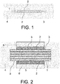
- Fig. 1 shows in a side view a power semiconductor device according to an exemplary implementation, which comprises a silicon or silicon carbide bipolar semiconductor wafer 1 having a disc-like shape with a diameter of 30 mm to 200 mm, and a respective thickness of 300 ⁇ m to 1500 ⁇ m.
- the semiconductor wafer 1 comprises two contact elements 2 as electric contacts respectively electrodes, which are arranged opposite to each other at the longitudinal surfaces of the disc-like shape, and are also referred to as main sides.
- the contact elements 2 are surrounded by junction terminations 3, which are arranged at lateral sides of the semiconductor wafer 1 between the opposite contact elements 2.
- the junction terminations 3 are diamond like carbon, DLC, passivated. Instead of DLC the passivation may comprise polyimide, epoxy mold compound, parylene, borosilicate glass, hydrophobic layer or phenol resin.
- the semiconductor wafers 1 are configured for use in high voltage application such as 1.2, 2.8, 3.3, 4.5, 5.2, 6.5, 7.2, 8.5 ,10 or 20 kV.
- the semiconductor wafer 1 is surrounded by an insulating medium 4 selected from the group consisting of a dielectric liquid, a pressurized dielectric gas and a vacuum, which thus hermetically seals the junction termination 3.
- the dielectric liquid is an organic or synthetic oil.
- the dielectric gas comprises sulfur hexafluoride, SF 6 , nitrogen, N 2 , dry air, fluorinated organic gases, or mixtures thereof.
- the pressurized dielectric gas requires a pressure of ⁇ 120 kPa and ⁇ 50 MPa, and in particular ⁇ 1 MPa.
- the vacuum requires a pressure ⁇ 10 -4 Pa.
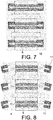
- Fig. 2 shows in a side view the semiconductor device according to a further exemplary implementation, whereby a plurality of semiconductor wafers 1 are arranged on top of each other.
- Two molybdenum discs are attached as top leadframe respectively base leadframe 5 on both contact elements 2.
- Two metal housing pole pieces are attached as top plate respectively base plate 6 onto the top leadframe respectively base leadframe 5 such that the top plate and the base plate 6 'sandwich' the top leadframe and base leadframe 5, whereas the latter two 'sandwich' the semiconductor wafer 1.
- the semiconductor wafer 1 overtops on both sides with the junction terminations 3 the top leadframe and base leadframe 5.
- Top plate and/or the base plate 6 comprise a cooler element 9, not explicitly shown in Fig. 2 , for cooling the semiconductor wafer 1.
- Top plate and/or the base plate 6 are also referred to as cooler.
- Fig. 3 shows in a side view the semiconductor device according to a further exemplary implementation, whereas two semiconductor wafers 1 are arranged besides each other and connected in series.
- each semiconductor wafer 1 is electrically 'sandwiched' between the top leadframe and base leadframe 5.
- Top leadframe and base leadframe 5 are also electrically 'sandwiched' between top plate and the base plate 6.
- base plate 6 of the left semiconductor device is provided one piece and thus connected with the top 6 of the right semiconductor device for forming the series connection.
- the top plate 6 of the left semiconductor device and the base plate 6 of the right semiconductor device form electrical contacts for connection the semiconductor devices.
- Both semiconductor devices are arranged via an insulating layer 7 on a base 8.
- Fig. 4 shows in a side view the semiconductor device according to a further exemplary implementation, whereby three semiconductor devices are directly stacked on top of each other.
- a separate cooler element 9 is provided between each base plate 6 of the upper semiconductor device and the top plate 6 of the lower semiconductor device comprising cooling channels.
- Figs. 5 to 7 show in a side view semiconductor devices according to a further exemplary implementation, whereas the semiconductor devices relate to the implementations as described before in respect to Figs. 2 to 4 .
- a junction termination ring 10 is provided which laterally encapsulates the junction termination 3 of the respective semiconductor wafer 1.
- the junction termination ring 10 comprises an oil-compatible material such as epoxy or hybrid epoxy with an imide compound, or other corrosive gas- or vacuum-compatible material. Due to the junction termination ring 10, the housing-less semiconductor wafers 1 are centered while clamped in a stack.
- the junction termination ring 10 laterally encapsulates all semiconductor wafers 1 arranged one above the other.
- the junction termination ring 10 also encapsulates the base leadframe and the top leadframe 5, and the base plates 6 of the two semiconductor devices.
- each semiconductor wafer 1 is encapsulated at its lateral junction terminations 3 with said junction termination ring 10.
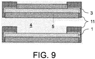
- Fig. 8 shows in a side view the semiconductor device according to a further exemplary implementation, which corresponds to the implementation shown in Fig. 7 .
- an alignment ring 11 is provided for centering the semiconductor wafers 1 arranged in a stack.
- the alignment ring 11 also comprises a U-shape in side view, but is removed from the semiconductor wafers 1 after assembly of the semiconductor wafers 1 into the stack.
- Other shapes may include an L-shape or an asymmetric shape, as can be seen in Fig. 9 showing two possible implementations having an L-shape.
- the described power semiconductor can be advantageously used for example in a subsea converter, a transformer tap changer or a high voltage direct current converter, or within a next generation HVDC compact converters, and other oil-containing or pressurized gas-containing applications.
- the insulating medium is 'housed' respectably encapsulated by a respective housing of the converter, tap changer or the application.
- thin housing flanges extend from the top plate respectively the base plate 6 usually lack mechanical stability if the stack was to be immersed deep under water or in outer space with high vacuum.
- the proposed 'housing less' power semiconductor device is tolerant against high hydrostatic external pressure above atmospheric pressure, or high vacuum below 10 -4 Pa.
Landscapes
- Formation Of Insulating Films (AREA)
Abstract
Description
- The invention relates to power semiconductor device, comprising a semiconductor wafer having at least one contact element and a passivated junction termination laterally surrounding the at least one contact element. The present invention also relates to a use of the power semiconductor device.
- Bipolar diode and thyristor power semiconductor devices are considered attractive as potential power semiconductors devices for subsea converters, transformer tap-changers and other oil immersed electronics systems, or next generation high-voltage, direct current, HVDC, compact converters, or high vacuum power generation space applications.
- Discrete bipolar power semiconductor devices are typically packaged in a rubber protection around its junction termination and passivation and, when hermetically packed, then in atmospheric pressure. In application, the semiconductor wafer itself is mounted into a copper-ceramic housing between two molybdenum disks. Said housing-mounted semiconductor elements are inserted between coolers to form stacks, or are already clamped within a module, which are then used as parts of said converters and tap changers.
- When an electric field at a p-n junction in an active region of the power semiconductor device reaches a critical value of the electric field for silicon Ecrit≈200 kV/cm, an excessive impact ionization causes an electrical breakdown. When the p-n junction reaches a surface of the power semiconductor device and the electric field exceeds a dielectric strength Emax of an ambient dielectric, such as air, nitrogen, vacuum, oil etc., the dielectric breakdown occurs. The high electric field ionizes molecules and changes them from an insulator to a conductor. Because of the recombination of electrons and ions, sparks occur and the required blocking capability is lost. As the dry air or nitrogen shows only Emax ≤30 kV/cm, the edge of the semiconductor wafer or chip must be specially treated against the dielectric breakdown. Said part of the semiconductor wafer is called junction termination and represents the most sensitive region regarding t blocking capability and its long-term stability.
- Today's power semiconductor devices configuration, however, are not tolerant against high hydrostatic external pressure i.e. higher than atmospheric pressure, or high vacuum, because typically thin housing flanges extending from pole pieces are lacking mechanical stability if the stack was to be immersed deep under water or in outer space with high vacuum.
- It is therefore an object of the invention to provide a power semiconductor device that is tolerant against high hydrostatic external pressure and/or high vacuum.
- The object of the invention is solved by the features of the independent claims. Modified implementations are detailed in the dependent claims.
- Thus, the object is solved by a power semiconductor device, comprising
- a semiconductor wafer having at least one contact element and a passivated junction termination laterally surrounding the at least one contact element, and
- an isolating medium selected from the group consisting of a dielectric liquid, a pressurized dielectric gas and a vacuum, wherein
- the semiconductor wafer is immersed and/or surrounded by the insulating medium.
- It is therefore a key point that the semiconductor wafer is surrounded by the dielectric liquid, the pressurized dielectric gas or the vacuum. Such way the power semiconductor device is tolerant against high hydrostatic external pressure, in particular higher than atmospheric pressure or high vacuum. Thereby the power semiconductor device may only use materials compatible with the dielectric liquid, such as for example organic or synthetic oil, pressurized gas or high vacuum. Such ways the proposed power semiconductor device can advantageously be used in oil-containing applications, in pressurized gas-containing applications and in high vacuum-environment applications by immersion of the semiconductor wafer in the above specified insulating medium.
- The semiconductor wafer can be provided 'housing-less' i.e. does not require any housing in particular directly enclosing the semiconductor wafer such that manufacturing becomes easier. The dielectric liquid, pressurized gas or vacuum assures that creepage and strike distance requirements are met. HTRB, high temperature reverse bias, tests have readily shown that semiconductor wafers such as for example diodes are functional if the insulating medium covers the contact element and passivated junction termination. The semiconductor device may be installed in a subsea converter, a transformer tap changer or a high voltage direct current converter, or in any other appliance. Said converter of appliance may comprise a housing, which 'houses' the dielectric liquid.
- The semiconductor wafer may comprise a disc like shape with longitudinal surfaces. Opposite longitudinal surfaces of the semiconductor wafer may form opposite contact elements i.e. electrical contacts, whereas the junction termination is arranged at the lateral side between the opposite contact elements. The contact elements, for example anode, cathode and gate regions of the power semiconductor device, can be provided with a copper metallization, aluminum metallization or other high conductive metals as electrical contacts and/or electrodes. Passivated means that the surface of the semiconductor wafer is rendered inert, and thus does not change semiconductor properties as a result of interaction with air or other materials in contact with the surface or edge of the crystal. Passivation can also mean that a silicon surface of the semiconductor wafer is shielded from external charges, also referred to as electro-active passivation. Passivation is typically achieved using a form of thermal oxidation, for example by oxidation to a coating of silicon dioxide or by deposition of a layer with electro-passivation properties. The semiconductor wafer being immersed and/or surrounded by the isolating medium means that the semiconductor wafer is at least partially or completely immersed and/or surrounded by the isolating medium. The semiconductor wafer may further comprise at least one junction.
- According to a modified implementation, the isolating medium hermetically seals the junction termination and/or the contact element. Thus, at least the junction termination is for example completely surrounded by the isolating medium, which such ways hermetically seals the junction termination. Thereby the junction termination can be in direct contact with the isolating medium.
- According to a further modified implementation, the dielectric liquid is an organic or synthetic oil. The dielectric liquid may comprise mineral oil, silicone oil, n-Hexane, n-Heptane or other dielectric liquid known to the person skilled in the art that provide electrical insulation and thus suppress corona and arcing. In this respect gels are not considered to constitute insulating mediums.
- According to another modified implementation, the pressurized dielectric gas comprises one of sulfur hexafluoride, SF6, nitrogen, N2, dry air, fluorinated organic gases, and mixtures comprising at least one of the before mentioned components, and/or wherein the pressurized dielectric gas comprises a pressure of ≥ 120 kPa and ≤ 50 MPa. The pressure can also be in the range of ≥ 120 kPa and ≤ 1 MPa. Humidity level of said gases can be limited to a value to avoid condensation at a given pressure and minimum operating temperature, such as at 0 °C. Fluorinated organic gases may comprise perfluorohexane or other fluorinated organic gases known to the person skilled in the art. The pressurized dielectric gas may also comprise Fluorinert™ or AirPlus gas mixture, in particular C5-Fluoroketone (C5 FK). Beside that any dielectric gas can be used that provides electrical insulation and thus suppresses corona and arcing.
- In a further modified implementation, the vacuum has a pressure ≤ 10-4 Pa. The pressure may also be ≤ 10-2 Pa, ≤ 10-3 Pa, ≤ 10-5 Pa or ≤ 10-6 Pa. Vacuum means in particular that a mean free path, MFP, of residual gases is longer than the size of the chamber or of the object under test.
- According to another modified implementation, the passivation comprises at least one of diamond-like carbon, polyimide, epoxy mold compound, parylene, borosilicate glass, hydrophobic layer and phenol resin. The phenol resin can be provided as WPR and may comprise rubber particles, for such way providing reliable insulation and high dielectric strength in the range of 380 kV/mm. Diamond-like carbon can be provided as thin film carbon coating, in particular as plasma polymer films, amorphous carbon films, CVD diamond films as well as graphite films. Said carbon films can be manufactured by deposition using a gas-phase deposition processes in most cases taking place in a vacuum by using chemical vapor deposition, CVD or physical vapor deposition, PVD. The film thicknesses are typically a few hundred nanometers for diamond like carbon, DLC, passivation or up to tens of micrometers for polyimide.
- According to a further modified implementation, the semiconductor wafer is provided as silicon or silicon carbide bipolar wafer. The semiconductor wafer, also called a slice or substrate, is often a thin slice of semiconductor such as a crystalline silicon (c-Si), GaN or other semiconductor materials. A semiconductor wafer has typically a round shape with a diameter of 30 mm to 450 mm, for example 30 mm to 150 mm, and a respective thickness of 300 µm to 1500 µm, and is thus often referred to as disc or disc-like wafer.
- According to another modified implementation, the power semiconductor device comprises a top leadframe and a base leadframe, whereby the semiconductor wafer is sandwiched between the top leadframe and the base leadframe, and the top leadframe. The power semiconductor device may further comprise a top plate and a base plate, whereby the semiconductor wafer and the base leadframe are sandwiched between the top plate and the base plate. The semiconductor wafer may, in side view, overtop the top plate, the base plate, the top leadframe and the base leadframe on both sides. The top plate, the base plate, the top leadframe and the base leadframe may have a corresponding shape and/or an equal shape as the semiconductor wafer, for example a round respectively disc or disc-like shape. The top leadframe may be directly, gap-free and/or touching attached to the top plate and/or to the semiconductor wafer, for example by bonding or the like. The base leadframe may be directly, gap-free and/or touching attached to the semiconductor wafer and/or the base plate, for example by bonding (soldering, sintering, adhesive bonding) or the like. The top plate and the base plate can be provided as metal plates.
- In a further modified implementation, the top leadframe and/or the base leadframe are provided as molybdenum discs. Alternatively, the top leadframe and/or the base leadframe may comprise Cu or CuMo. The base leadframe and/or the top leadframe can be provided as thick-metal leadframes. The base leadframe and/or the top leadframe can be based on Cu and bonding can be conducted by sintering into cavities of the respective leadframe.
- According to another modified implementation, the top plate and/or the base plate are provided as cooling elements and/or as heatsinks for cooling the semiconductor wafer. The cooling elements may comprise a moving fluid, for example, air, cooling gas or liquid, or a cooling channel. In such regard the base plate and/or the top plate are also referred to as cooler. Thus, cooling capability can be supplied to both sides of the semiconductor wafer.
- In a further modified implementation, the power semiconductor device comprises a plurality of semiconductor wafers arranged on top of each other. The semiconductor wafers can be directly, gap-free and/or touching arranged to each other. Such way the plurality of semiconductor wafers is stacked.
- According to another modified implementation, the power semiconductor device comprises a junction termination ring or an alignment ring encapsulating the junction terminations of the semiconductor wafers. According to a further modified implementation, the junction termination ring or the alignment ring comprises, in side view, a U-shape. The junction termination ring or the alignment ring may also comprise an asymmetric shape, for example an L-shape. The junction termination ring may comprise an oil-compatible material, such as for example Epoxy, Hybrid Epoxy with an imide compound, or other corrosive gas- or vacuum-compatible material. The housing-less semiconductor wafers clamped in a stack can be easily centered with the junction termination ring. Such housing-less semiconductor wafers with an oil-compatible junction termination ring can be readily manufactured by using a single-step transfer molding process with epoxy-molding compound. Power semiconductor device material compatibility with the environment medium, for example dielectric liquid, is necessary, so that impurities are not released, for example when materials soak in the oil or other insulating mediums, especially when temperature increases. However, diamond like carbon material and composition of the materials used for junction termination ring showed readily good compatibility with organic oil both under room and elevated temperatures (such as 125°C). The alignment ring can be added to the semiconductor wafer and removed from the semiconductor wafer after assembly into a stack.
- The object is further solved by a use of the power semiconductor device as described before in a subsea converter, a transformer tap changer or a high voltage direct current converter. The proposed 'housing less' power semiconductor device can be advantageously used for subsea converters and transformer tap changers, or next generation HVDC compact converters, high vacuum power generations space applications and other oil-containing or pressurized gas-containing applications, as the power semiconductor device is tolerant against high hydrostatic external pressure above atmospheric pressure, or high vacuum below for example 10-4 Pa.
- The object is even further solved by method for manufacturing a power semiconductor device, comprising
- a semiconductor wafer having at least one contact element and a passivated junction termination laterally surrounding the at least one contact element, and
- an insulating medium selected from the group consisting of a dielectric liquid, a pressurized dielectric gas and a vacuum, and comprising the step of
- immersing and/or surrounding the semiconductor wafer by the insulating medium.
- Further implementations and advantages of the use and of the method are directly and unambiguously derived by the person skilled in the art from the device as described before.
- These and other aspects of the invention will be apparent from and elucidated with reference to the implementations described hereinafter.
- In the drawings:
-
Fig. 1 shows in a side a view a power semiconductor device according to an exemplary implementation, -
Fig. 2 shows in a side view the power semiconductor device according to a further exemplary implementation, -
Fig. 3 shows in a side view the power semiconductor device according to a further exemplary implementation, -
Fig. 4 shows in a side view the power semiconductor device according to a further exemplary implementation, -
Fig. 5 shows in a side view the power semiconductor device according to a further exemplary implementation, whereas the implementation corresponds to the implementation shown inFig. 2 , -
Fig. 6 shows in a side view the power semiconductor device according to a further exemplary implementation, whereas the implementation corresponds to the implementation shown inFig. 3 , -
Fig. 7 shows in a side view the power semiconductor device according to a further exemplary implementation, whereas the implementation corresponds to the implementation shown inFig. 4 , -
Fig. 8 shows in a side view the power semiconductor device according to a further exemplary implementation, whereas the implementation corresponds to the implementation shown inFig. 7 , and -
Fig. 9 shows in a side view the power semiconductor device according to two further exemplary implementation. -
Fig. 1 shows in a side view a power semiconductor device according to an exemplary implementation, which comprises a silicon or silicon carbidebipolar semiconductor wafer 1 having a disc-like shape with a diameter of 30 mm to 200 mm, and a respective thickness of 300 µm to 1500 µm. - The
semiconductor wafer 1 comprises twocontact elements 2 as electric contacts respectively electrodes, which are arranged opposite to each other at the longitudinal surfaces of the disc-like shape, and are also referred to as main sides. Thecontact elements 2 are surrounded byjunction terminations 3, which are arranged at lateral sides of thesemiconductor wafer 1 between theopposite contact elements 2. Thejunction terminations 3 are diamond like carbon, DLC, passivated. Instead of DLC the passivation may comprise polyimide, epoxy mold compound, parylene, borosilicate glass, hydrophobic layer or phenol resin. Thesemiconductor wafers 1 are configured for use in high voltage application such as 1.2, 2.8, 3.3, 4.5, 5.2, 6.5, 7.2, 8.5 ,10 or 20 kV. - The
semiconductor wafer 1 is surrounded by an insulatingmedium 4 selected from the group consisting of a dielectric liquid, a pressurized dielectric gas and a vacuum, which thus hermetically seals thejunction termination 3. Such way the semiconductor device is provided 'without' a housing. The dielectric liquid is an organic or synthetic oil. The dielectric gas comprises sulfur hexafluoride, SF6, nitrogen, N2, dry air, fluorinated organic gases, or mixtures thereof. The pressurized dielectric gas requires a pressure of ≥ 120 kPa and ≤ 50 MPa, and in particular ≤ 1 MPa. The vacuum requires a pressure ≤ 10-4 Pa. -
Fig. 2 shows in a side view the semiconductor device according to a further exemplary implementation, whereby a plurality ofsemiconductor wafers 1 are arranged on top of each other. Two molybdenum discs are attached as top leadframe respectivelybase leadframe 5 on bothcontact elements 2. Two metal housing pole pieces are attached as top plate respectivelybase plate 6 onto the top leadframe respectivelybase leadframe 5 such that the top plate and the base plate 6 'sandwich' the top leadframe andbase leadframe 5, whereas the latter two 'sandwich' thesemiconductor wafer 1. Thesemiconductor wafer 1 overtops on both sides with thejunction terminations 3 the top leadframe andbase leadframe 5. Top plate and/or thebase plate 6 comprise acooler element 9, not explicitly shown inFig. 2 , for cooling thesemiconductor wafer 1. Thus, Top plate and/or thebase plate 6 are also referred to as cooler. -
Fig. 3 shows in a side view the semiconductor device according to a further exemplary implementation, whereas twosemiconductor wafers 1 are arranged besides each other and connected in series. As described before, eachsemiconductor wafer 1 is electrically 'sandwiched' between the top leadframe andbase leadframe 5. Top leadframe andbase leadframe 5 are also electrically 'sandwiched' between top plate and thebase plate 6. However,base plate 6 of the left semiconductor device is provided one piece and thus connected with thetop 6 of the right semiconductor device for forming the series connection. Such way thetop plate 6 of the left semiconductor device and thebase plate 6 of the right semiconductor device form electrical contacts for connection the semiconductor devices. Both semiconductor devices are arranged via an insulatinglayer 7 on abase 8. -
Fig. 4 shows in a side view the semiconductor device according to a further exemplary implementation, whereby three semiconductor devices are directly stacked on top of each other. A separatecooler element 9 is provided between eachbase plate 6 of the upper semiconductor device and thetop plate 6 of the lower semiconductor device comprising cooling channels. -
Figs. 5 to 7 show in a side view semiconductor devices according to a further exemplary implementation, whereas the semiconductor devices relate to the implementations as described before in respect toFigs. 2 to 4 . In addition to the implementations described before, ajunction termination ring 10 is provided which laterally encapsulates thejunction termination 3 of therespective semiconductor wafer 1. Thejunction termination ring 10 comprises an oil-compatible material such as epoxy or hybrid epoxy with an imide compound, or other corrosive gas- or vacuum-compatible material. Due to thejunction termination ring 10, thehousing-less semiconductor wafers 1 are centered while clamped in a stack. - As shown in
Fig. 5 , thejunction termination ring 10 laterally encapsulates allsemiconductor wafers 1 arranged one above the other. InFig. 6 , wherein thesemiconductor wafers 1 do not overtop in longitudinal direction the base leadframe and thetop leadframe 5, thejunction termination ring 10 also encapsulates the base leadframe and thetop leadframe 5, and thebase plates 6 of the two semiconductor devices. In the implementation shown inFig. 7 , eachsemiconductor wafer 1 is encapsulated at itslateral junction terminations 3 with saidjunction termination ring 10. -
Fig. 8 shows in a side view the semiconductor device according to a further exemplary implementation, which corresponds to the implementation shown inFig. 7 . Instead of thejunction termination ring 10, analignment ring 11 is provided for centering thesemiconductor wafers 1 arranged in a stack. Thealignment ring 11 also comprises a U-shape in side view, but is removed from thesemiconductor wafers 1 after assembly of thesemiconductor wafers 1 into the stack. Other shapes may include an L-shape or an asymmetric shape, as can be seen inFig. 9 showing two possible implementations having an L-shape. - The described power semiconductor can be advantageously used for example in a subsea converter, a transformer tap changer or a high voltage direct current converter, or within a next generation HVDC compact converters, and other oil-containing or pressurized gas-containing applications. Thereby, the insulating medium is 'housed' respectably encapsulated by a respective housing of the converter, tap changer or the application. In prior art application thin housing flanges extend from the top plate respectively the
base plate 6 usually lack mechanical stability if the stack was to be immersed deep under water or in outer space with high vacuum. In contrast thereto the proposed 'housing less' power semiconductor device is tolerant against high hydrostatic external pressure above atmospheric pressure, or high vacuum below 10-4 Pa. - While the invention has been illustrated and described in detail in the drawings and foregoing description, such illustration and description are to be considered illustrative or exemplary and not restrictive; the invention is not limited to the disclosed implementations. Other variations to be disclosed implementations can be understood and effected by those skilled in the art in practicing the claimed invention, from a study of the drawings, the disclosure, and the appended claims. In the claims, the word "comprising" does not exclude other elements or steps, and the indefinite article "a" or "an" does not exclude a plurality. The mere fact that certain measures are recited in mutually different dependent claims does not indicate that a combination of these measures cannot be used to advantage. Any reference signs in the claims should not be construed as limiting scope.
-
- 1
- semiconductor wafer
- 2
- contact element
- 3
- junction termination
- 4
- insulating medium
- 5
- top leadframe, base leadframe
- 6
- top plate, base plate
- 7
- insulating layer
- 8
- base
- 9
- heat sink, cooler element
- 10
- junction termination ring
- 11
- alignment ring
Claims (15)
- A power semiconductor device, comprising
a semiconductor wafer (1) having at least one contact element (2) and a passivated junction termination (3) laterally surrounding the at least one contact element (2), and
an insulating medium (4) selected from the group consisting of a dielectric liquid, a pressurized dielectric gas and a vacuum, wherein
the semiconductor wafer (1) is surrounded by the insulating medium (4). - The power semiconductor device according to the previous claim, whereby the insulating medium (4) hermetically seals the junction termination (3).
- The power semiconductor device according to any of the previous claims, whereby the dielectric liquid is an organic or synthetic oil.
- The power semiconductor device according to any of the previous claims, whereby the pressurized dielectric gas comprises one of sulfur hexafluoride, SF6, nitrogen, N2, dry air, fluorinated organic gases, and mixtures comprising at least one of the before mentioned components, and/or wherein the pressurized dielectric gas comprises a pressure of ≥ 120 kPa and ≤ 50 MPa, in particular ≤ 1 MPa.
- The power semiconductor device according to any of the previous claims, whereby the vacuum has a pressure ≤ 10-4 Pa.
- The power semiconductor device according to any of the previous claims, whereby the passivation comprises at least one of diamond-like carbon, polyimide, epoxy mold compound, parylene, borosilicate glass, hydrophobic layer and phenol resin.
- The power semiconductor device according to any of the previous claims, whereby the semiconductor wafer (1) is provided as silicon or silicon carbide bipolar semiconductor wafer (1).
- The power semiconductor device according to any of the previous claims, comprising a top leadframe (5) and a base leadframe (5), whereby the semiconductor wafer (1) is sandwiched between the top leadframe (5) and the base leadframe (5), and/or comprising a top plate (6) and a base plate (6), whereby the top leadframe (5), the semiconductor wafer (1) and the base leadframe (5) are sandwiched between the top plate (6) and the base plate (6).
- The power semiconductor device according to the previous claim, whereby the top leadframe (5) and/or the base leadframe (5) are provided as molybdenum discs.
- The power semiconductor device according to any of the two previous claims, whereby the top plate (6) and/or the base plate (6) are provided as cooling elements (9) for cooling the semiconductor wafer (1).
- The power semiconductor device according to any of the previous claims, comprising a plurality of semiconductor wafers (1) arranged on top of each other.
- The power semiconductor device according to any of the previous claims, comprising a junction termination ring (10) or an alignment ring (11) encapsulating the junction termination (3) of the semiconductor wafer (1).
- The power semiconductor device according to the previous claim, whereby the junction termination ring (10) or the alignment ring (11) comprises, in side view, a U-shape or L-shape.
- Use of the power semiconductor device according to any of the previous claims in a subsea converter, a transformer tap changer or a high voltage direct current converter.
- Method for manufacturing power semiconductor device, comprising
a semiconductor wafer (1) having at least one contact element (2) and a passivated junction termination (3) laterally surrounding the at least one contact element (2), and
an insulating medium (4) selected from the group consisting of a dielectric liquid, a pressurized dielectric gas and a vacuum, and comprising the step of
surrounding the semiconductor wafer (1) by the insulating medium (4).
Priority Applications (1)
| Application Number | Priority Date | Filing Date | Title |
|---|---|---|---|
| EP20183145.0A EP3933907A1 (en) | 2020-06-30 | 2020-06-30 | Power semiconductor device |
Applications Claiming Priority (1)
| Application Number | Priority Date | Filing Date | Title |
|---|---|---|---|
| EP20183145.0A EP3933907A1 (en) | 2020-06-30 | 2020-06-30 | Power semiconductor device |
Publications (1)
| Publication Number | Publication Date |
|---|---|
| EP3933907A1 true EP3933907A1 (en) | 2022-01-05 |
Family
ID=71451973
Family Applications (1)
| Application Number | Title | Priority Date | Filing Date |
|---|---|---|---|
| EP20183145.0A Pending EP3933907A1 (en) | 2020-06-30 | 2020-06-30 | Power semiconductor device |
Country Status (1)
| Country | Link |
|---|---|
| EP (1) | EP3933907A1 (en) |
Citations (4)
| Publication number | Priority date | Publication date | Assignee | Title |
|---|---|---|---|---|
| US3413532A (en) * | 1965-02-08 | 1968-11-26 | Westinghouse Electric Corp | Compression bonded semiconductor device |
| JPS5683049A (en) * | 1979-12-11 | 1981-07-07 | Mitsubishi Electric Corp | Inspection of airtightness of semiconductor device |
| US5489802A (en) * | 1992-06-26 | 1996-02-06 | Mitsubishi Denki Kabushiki Kaisha | Pressure contact type semiconductor device and heat compensator |
| WO2014177553A1 (en) * | 2013-05-02 | 2014-11-06 | Abb Technology Ag | Pole-piece for a power semiconductor device |
-
2020
- 2020-06-30 EP EP20183145.0A patent/EP3933907A1/en active Pending
Patent Citations (4)
| Publication number | Priority date | Publication date | Assignee | Title |
|---|---|---|---|---|
| US3413532A (en) * | 1965-02-08 | 1968-11-26 | Westinghouse Electric Corp | Compression bonded semiconductor device |
| JPS5683049A (en) * | 1979-12-11 | 1981-07-07 | Mitsubishi Electric Corp | Inspection of airtightness of semiconductor device |
| US5489802A (en) * | 1992-06-26 | 1996-02-06 | Mitsubishi Denki Kabushiki Kaisha | Pressure contact type semiconductor device and heat compensator |
| WO2014177553A1 (en) * | 2013-05-02 | 2014-11-06 | Abb Technology Ag | Pole-piece for a power semiconductor device |
Similar Documents
| Publication | Publication Date | Title |
|---|---|---|
| US10134654B2 (en) | Double-encapsulated power semiconductor module and method for producing the same | |
| IE48638B1 (en) | Semiconductor package having strengthening and sealing upper chamber | |
| US10192800B2 (en) | Semiconductor device | |
| JP6526229B2 (en) | Power module | |
| US9349790B2 (en) | Power electronic devices | |
| US3601667A (en) | A semiconductor device with a heat sink having a foot portion | |
| EP3824497B1 (en) | Power semiconductor device | |
| US8981545B2 (en) | Explosion-protected semiconductor module | |
| EP3933907A1 (en) | Power semiconductor device | |
| US9601399B2 (en) | Module arrangement for power semiconductor devices | |
| CN114171575B (en) | semiconductor devices | |
| EP4080551A1 (en) | Semiconductor power module and method for manufacturing a semiconductor power module and semiconductor power device | |
| US8895994B2 (en) | Electronic device including silicon carbide diode dies | |
| JP7203214B2 (en) | Power semiconductor device with floating mounting | |
| US20220028768A1 (en) | Semiconductor device packages and methods of assembling thereof | |
| US20250014952A1 (en) | Housing, semiconductor module and methods for producing the same | |
| Lebey et al. | High temperature high voltage packaging of wideband gap semiconductors using gas insulating medium | |
| JP2000058693A (en) | Flat semiconductor device, method of manufacturing the same, and converter using the same | |
| US20250322985A1 (en) | Multi-substrate transformer packages with magnetostriction management | |
| US20250182950A1 (en) | Integrated transformer and ic packages | |
| JP2024123341A (en) | Power semiconductor device and its manufacturing method | |
| JP2003086764A (en) | Semiconductor device |
Legal Events
| Date | Code | Title | Description |
|---|---|---|---|
| PUAI | Public reference made under article 153(3) epc to a published international application that has entered the european phase |
Free format text: ORIGINAL CODE: 0009012 |
|
| STAA | Information on the status of an ep patent application or granted ep patent |
Free format text: STATUS: THE APPLICATION HAS BEEN PUBLISHED |
|
| AK | Designated contracting states |
Kind code of ref document: A1 Designated state(s): AL AT BE BG CH CY CZ DE DK EE ES FI FR GB GR HR HU IE IS IT LI LT LU LV MC MK MT NL NO PL PT RO RS SE SI SK SM TR |
|
| B565 | Issuance of search results under rule 164(2) epc |
Effective date: 20201102 |
|
| STAA | Information on the status of an ep patent application or granted ep patent |
Free format text: STATUS: REQUEST FOR EXAMINATION WAS MADE |
|
| 17P | Request for examination filed |
Effective date: 20220624 |
|
| RBV | Designated contracting states (corrected) |
Designated state(s): AL AT BE BG CH CY CZ DE DK EE ES FI FR GB GR HR HU IE IS IT LI LT LU LV MC MK MT NL NO PL PT RO RS SE SI SK SM TR |