EP3933841A1 - Repair circuit, memory, and repair method - Google Patents
Repair circuit, memory, and repair method Download PDFInfo
- Publication number
- EP3933841A1 EP3933841A1 EP21761667.1A EP21761667A EP3933841A1 EP 3933841 A1 EP3933841 A1 EP 3933841A1 EP 21761667 A EP21761667 A EP 21761667A EP 3933841 A1 EP3933841 A1 EP 3933841A1
- Authority
- EP
- European Patent Office
- Prior art keywords
- repair
- target
- memory area
- bits
- circuit
- Prior art date
- Legal status (The legal status is an assumption and is not a legal conclusion. Google has not performed a legal analysis and makes no representation as to the accuracy of the status listed.)
- Granted
Links
Images




Classifications
-
- G—PHYSICS
- G11—INFORMATION STORAGE
- G11C—STATIC STORES
- G11C29/00—Checking stores for correct operation ; Subsequent repair; Testing stores during standby or offline operation
- G11C29/70—Masking faults in memories by using spares or by reconfiguring
- G11C29/76—Masking faults in memories by using spares or by reconfiguring using address translation or modifications
-
- G—PHYSICS
- G11—INFORMATION STORAGE
- G11C—STATIC STORES
- G11C29/00—Checking stores for correct operation ; Subsequent repair; Testing stores during standby or offline operation
- G11C29/04—Detection or location of defective memory elements, e.g. cell constructio details, timing of test signals
- G11C29/08—Functional testing, e.g. testing during refresh, power-on self testing [POST] or distributed testing
- G11C29/12—Built-in arrangements for testing, e.g. built-in self testing [BIST] or interconnection details
- G11C29/44—Indication or identification of errors, e.g. for repair
-
- G—PHYSICS
- G11—INFORMATION STORAGE
- G11C—STATIC STORES
- G11C29/00—Checking stores for correct operation ; Subsequent repair; Testing stores during standby or offline operation
- G11C29/04—Detection or location of defective memory elements, e.g. cell constructio details, timing of test signals
- G11C29/08—Functional testing, e.g. testing during refresh, power-on self testing [POST] or distributed testing
- G11C29/12—Built-in arrangements for testing, e.g. built-in self testing [BIST] or interconnection details
- G11C29/44—Indication or identification of errors, e.g. for repair
- G11C29/4401—Indication or identification of errors, e.g. for repair for self repair
-
- G—PHYSICS
- G11—INFORMATION STORAGE
- G11C—STATIC STORES
- G11C29/00—Checking stores for correct operation ; Subsequent repair; Testing stores during standby or offline operation
- G11C29/04—Detection or location of defective memory elements, e.g. cell constructio details, timing of test signals
- G11C29/08—Functional testing, e.g. testing during refresh, power-on self testing [POST] or distributed testing
- G11C29/12—Built-in arrangements for testing, e.g. built-in self testing [BIST] or interconnection details
- G11C29/38—Response verification devices
-
- G—PHYSICS
- G11—INFORMATION STORAGE
- G11C—STATIC STORES
- G11C29/00—Checking stores for correct operation ; Subsequent repair; Testing stores during standby or offline operation
- G11C29/52—Protection of memory contents; Detection of errors in memory contents
-
- G—PHYSICS
- G11—INFORMATION STORAGE
- G11C—STATIC STORES
- G11C29/00—Checking stores for correct operation ; Subsequent repair; Testing stores during standby or offline operation
- G11C29/70—Masking faults in memories by using spares or by reconfiguring
- G11C29/72—Masking faults in memories by using spares or by reconfiguring with optimized replacement algorithms
-
- G—PHYSICS
- G11—INFORMATION STORAGE
- G11C—STATIC STORES
- G11C29/00—Checking stores for correct operation ; Subsequent repair; Testing stores during standby or offline operation
- G11C29/70—Masking faults in memories by using spares or by reconfiguring
- G11C29/78—Masking faults in memories by using spares or by reconfiguring using programmable devices
- G11C29/783—Masking faults in memories by using spares or by reconfiguring using programmable devices with refresh of replacement cells, e.g. in DRAMs
-
- G—PHYSICS
- G11—INFORMATION STORAGE
- G11C—STATIC STORES
- G11C29/00—Checking stores for correct operation ; Subsequent repair; Testing stores during standby or offline operation
- G11C29/70—Masking faults in memories by using spares or by reconfiguring
- G11C29/78—Masking faults in memories by using spares or by reconfiguring using programmable devices
- G11C29/80—Masking faults in memories by using spares or by reconfiguring using programmable devices with improved layout
- G11C29/804—Masking faults in memories by using spares or by reconfiguring using programmable devices with improved layout to prevent clustered faults
-
- G—PHYSICS
- G11—INFORMATION STORAGE
- G11C—STATIC STORES
- G11C29/00—Checking stores for correct operation ; Subsequent repair; Testing stores during standby or offline operation
- G11C29/70—Masking faults in memories by using spares or by reconfiguring
- G11C29/78—Masking faults in memories by using spares or by reconfiguring using programmable devices
- G11C29/80—Masking faults in memories by using spares or by reconfiguring using programmable devices with improved layout
- G11C29/81—Masking faults in memories by using spares or by reconfiguring using programmable devices with improved layout using a hierarchical redundancy scheme
-
- H—ELECTRICITY
- H03—ELECTRONIC CIRCUITRY
- H03K—PULSE TECHNIQUE
- H03K19/00—Logic circuits, i.e. having at least two inputs acting on one output; Inverting circuits
- H03K19/20—Logic circuits, i.e. having at least two inputs acting on one output; Inverting circuits characterised by logic function, e.g. AND, OR, NOR, NOT circuits
-
- G—PHYSICS
- G11—INFORMATION STORAGE
- G11C—STATIC STORES
- G11C29/00—Checking stores for correct operation ; Subsequent repair; Testing stores during standby or offline operation
- G11C29/04—Detection or location of defective memory elements, e.g. cell constructio details, timing of test signals
- G11C2029/0409—Online test
-
- G—PHYSICS
- G11—INFORMATION STORAGE
- G11C—STATIC STORES
- G11C29/00—Checking stores for correct operation ; Subsequent repair; Testing stores during standby or offline operation
- G11C29/04—Detection or location of defective memory elements, e.g. cell constructio details, timing of test signals
- G11C29/08—Functional testing, e.g. testing during refresh, power-on self testing [POST] or distributed testing
- G11C29/12—Built-in arrangements for testing, e.g. built-in self testing [BIST] or interconnection details
- G11C2029/1202—Word line control
-
- G—PHYSICS
- G11—INFORMATION STORAGE
- G11C—STATIC STORES
- G11C29/00—Checking stores for correct operation ; Subsequent repair; Testing stores during standby or offline operation
- G11C29/70—Masking faults in memories by using spares or by reconfiguring
- G11C29/78—Masking faults in memories by using spares or by reconfiguring using programmable devices
- G11C29/785—Masking faults in memories by using spares or by reconfiguring using programmable devices with redundancy programming schemes
Definitions
- the disclosure relates to the technical field of semiconductor memories, and more particularly, to a repair circuit, a memory, and a repair method.
- DRAM Dynamic Random Access Memory
- DRAM arrays are typically stored to a normal memory area and a redundant memory area.
- a memory cell of the normal memory area cannot provide the normal read-write or storage function
- a memory cell of the redundant memory area may be used to replace the abnormal memory cell, thereby ensuring normal work of the memory.
- An objective of the disclosure is to provide a repair circuit, a memory, and a repair method, so as to at least overcome, to some extent, the reduction in the utilization rate of the redundant memory area due to the memory cell closest to the normal memory area in the redundant memory area cannot be used.
- a repair circuit is provided, which is disposed in a memory including a normal memory area and a redundant memory area, the redundant memory area including a target repair unit immediately adjacent to the normal memory area, and the repair circuit being configured to control the target repair unit to repair an abnormal memory cell in the normal memory area.
- the repair circuit includes a first control circuit and a repair determination module.
- the first control circuit is configured to receive signals at a target number of bits from low to high in a row address, process the signals at the target number of bits to obtain a control result, and output the control result.
- the target number is associated with a number of Word Lines (WLs) in the target repair unit.
- the repair determination module is connected to an output terminal of the first control circuit, and configured to receive the control result and output, in combination with the control result, a repair signal indicating whether to perform a repair operation.
- the repair determination module may include: a comparison circuit, configured to receive signals at rest bits other than the target number of bits in the row address, receive a fuse address, compare the signals at the rest bits with the fuse address bit by bit to obtain multiple comparison results, and output the multiple comparison results; and a second control circuit, connected to the output terminal of the first control circuit and an output terminal of the comparison circuit, and configured to receive the control result and the multiple comparison results, process the control result and the multiple comparison results, and output the repair signal indicating whether to perform the repair operation.
- a comparison circuit configured to receive signals at rest bits other than the target number of bits in the row address, receive a fuse address, compare the signals at the rest bits with the fuse address bit by bit to obtain multiple comparison results, and output the multiple comparison results
- a second control circuit connected to the output terminal of the first control circuit and an output terminal of the comparison circuit, and configured to receive the control result and the multiple comparison results, process the control result and the multiple comparison results, and output the repair signal indicating whether to perform the repair operation.
- the first control circuit may include: the target number of NOT gates, an input terminal of each of the target number of NOT gates receiving a respective one of the signals at the target number of bits from low to high in the row address; and an NAND gate, an input terminal of the NAND gate being connected to an output terminal of each of the target number of NOT gates, and an output terminal of the NAND gate being connected to the second control circuit, and configured to output the control result.
- the comparison circuit may include: multiple XNOR gates, a number of the multiple XNOR gates being the same as the number of the signals at the rest bits other than the target number of bits in the row address, a first input terminal of each of the multiple XNOR gates receiving a respective one of the signals at the rest bits other than the target number of bits in the row address, a second end of the each XNOR gate receiving a corresponding bit of the fuse address, and an output terminal of the each XNOR gate outputting a respective one of the multiple comparison results.
- the second control circuit may include: an AND gate, multiple first input terminals of the AND gate being connected to output terminals of the multiple XNOR gates, respectively, a second input terminal of the AND gate being connected to the output terminal of the NAND gate, and an output terminal of the AND gate outputting a repair signal indicating whether to perform the repair operation.
- the target number is n, the n being a positive integer greater than or equal to 2.
- the repair determination module when the signals at the target number of bits are all at a low level, the repair determination module outputs a repair signal indicating that no repair operation is to be performed.
- a memory which includes: a normal memory area; a redundant memory area, including a target repair unit immediately adjacent to the normal memory area; a row address receiving end, configured to receive a row address input to the memory; and the above any repair circuit.
- the memory may further include: a fuse address storage module, configured to store an address of a WL corresponding to an abnormal memory cell in the normal memory area as a fuse address, where the repair circuit is configured to receive the fuse address, so as to output a repair signal indicating whether to perform a repair operation.
- a fuse address storage module configured to store an address of a WL corresponding to an abnormal memory cell in the normal memory area as a fuse address
- the repair circuit is configured to receive the fuse address, so as to output a repair signal indicating whether to perform a repair operation.
- an address of a first WL in the abnormal memory cell is not stored.
- a repair method is provided, which is applied to a memory including a normal memory area and a redundant memory area, the redundant memory area including a target repair unit immediately adjacent to the normal memory area, and the repair method including that: a row address input to the memory is received; a control result is obtained according to signals at a target number of bits from low to high in the row address, where the target number is associated with a number of WLs in the target repair unit; and in combination with the control result, the target repair unit is controlled to repair an abnormal memory cell in the normal memory area.
- the operation that in combination with the control result, the target repair unit is controlled to repair the abnormal memory cell in the normal memory area may include that: signals at rest bits other than the target number of bits in the row address are determined; a fuse address corresponding to the abnormal memory cell in the normal memory area is received; the signals at the rest bits are compared with the fuse address bit by bit to obtain multiple comparison results; and according to the multiple comparison results and the control result, the target repair unit is controlled to repair the abnormal memory cell in the normal memory area.
- the operation that according to the multiple comparison results and the control result, the target repair unit is controlled to repair the abnormal memory cell in the normal memory area may include that: when at least one signal among the signals at the target number of bits from low to high in the row address is at a high level, the abnormal memory cell is repaired with the target repair unit; and when the signals at the target number of bits from low to high in the row address are all at a low level, the abnormal memory cell is repaired with a repair unit other than the target repair unit in the redundant memory area.
- the operation that the abnormal memory cell is repaired with the target repair unit may include that: a WL corresponding to the abnormal memory cell is replaced with a rest WL other than a first WL in the target repair unit; and a first WL of the abnormal memory cell is retained, where the first WL of the target repair unit is a WL adjacent to the normal memory area.
- the repair circuit includes a first control circuit and a repair determination module
- the first control circuit is configured to receive signals at the target number of bits from low to high in a row address and output a control result
- the repair determination module outputs, in combination with the control result, a repair signal indicating whether to perform a repair operation.
- the increasingly higher accuracy and the increasingly smaller size require that more structures are integrated on one chip. In this case, interference easily occurs between memory cells, and the row hammer phenomenon may occur.
- the row hammer may be understood as that when one Word Line (WL) is intensively accessed (for example, repeated read and write operations or maliciously attacked), charges stored in an adjacent memory cell may be affected to change from 0 to 1 or from 1 to 0, and such a random flipping will cause errors in the storage data.
- WL Word Line
- the WL used herein is usually used for controlling an on-off state of a memory cell. For example, when the WL is at a high level, the corresponding memory cell is on; and when the WL is at a low level, the corresponding memory cell is off.
- a repair unit in the redundant memory area may be used for repair.
- the usual repair process is to use multiple continuous WLs in the redundant memory area to replace the abnormal WLs at the same time.
- the multiple continuous WLs correspond to one repair unit.
- a repair unit adjacent to the normal memory area in the redundant memory area is not used. Hence, the influence of the adjacent repair unit on the normal memory area is avoided, and the row hammer problem is solved to some extent.
- the memory in the exemplary embodiment of the disclosure may include a normal memory area 11 and a redundant memory area 10.
- the normal memory area 11 includes N+1 WLs in total such as WL0, WL1, WL2, ..., WLN.
- the redundant memory area 10 includes M+1 WLs in total such as RWL0, RWL1, RWL2, ..., RWLM.
- the M is usually less than N.
- the repair unit 0 includes RWL0, RWL1, RWL2 and RWL3. If two continuous WLs in the normal memory area 11 are damaged, four WLs of the repair unit in the redundant memory area can be used to replace the two damaged WLs and the two adjacent WLs (that is, four WLs in total are replaced). Or, if two continuous WLs in the normal memory area 11 are damaged, a normal unit(s) corresponding to the two WLs may be determined, and all WLs of the normal unit(s) corresponding to the two WLs are replaced with the repair unit as the unit.
- the inventor typically only the first WL in the repair unit adjacent to the normal memory area in the redundant memory area has an influence on the normal memory area; and corresponding to FIG. 1 , that is, the RWL0 of the repair unit 0 in the redundant memory area 10 usually has the row hammer problem.
- the repair unit 0 further includes RWL1, RWL2 and RWL3, these three WLs also do not participate in the repair operation. Therefore, the available resources are wasted.
- a solution in which rest WLs other than the WL adjacent to the normal memory area in the above repair unit 0 can participate in the repair process is proposed, to improve the utilization rate of the redundant memory area.
- an exemplary embodiment of the disclosure provides a repair circuit.
- the repair circuit is disposed in a memory.
- the memory may be, for example, the DRAM.
- the memory may further be a Double Data Rate Fourth Synchronous Dynamic Random Access Memory (DDR4 SDRAM). There are no limits made on the type of the memory in the disclosure.
- DDR4 SDRAM Double Data Rate Fourth Synchronous Dynamic Random Access Memory
- the memory may include a normal memory area and a redundant memory area.
- the redundant memory area is configured to repair an abnormity when a memory cell in the normal memory area is abnormal.
- the abnormity of the memory cell may refer to a case where a normal read-write service cannot be provided due to a short circuit or an open circuit in manufacture or later use.
- the normal memory area and the redundant memory area are exemplarily illustrated in FIG. 1 , and are not repeatedly described.
- a repair unit immediately adjacent to the normal memory area in the redundant memory area is referred to as a target repair unit.
- the target repair unit corresponds to the repair unit 0.
- the repair circuit provided by the exemplary embodiment of the disclosure may be configured to selectively control the target repair unit to repair the abnormal memory cell in the normal memory area.
- the repair circuit may include a first control circuit 21 and a repair determination module 22.
- the first control circuit 21 may be configured to receive signals at the target number of bits from low to high in an input row address. For example, in a case where the row address is 12 bits and is characterized as ⁇ 11:0>, being from low to high refers to from the 0 th bit to the 11 th bit.
- the target number is associated with the number of WLs in the target repair unit. If the number of WLs in the target repair unit is 2 n , the target number is n, the n being a positive integer greater than or equal to 2. For example, in a case where the repair unit illustrated in FIG. 1 includes 4 WLs, the target number is 2. However, it is to be understood that for different memories, the repair unit may include 8 or 16 WLs, and the target number is 3 or 4, respectively.
- the first control circuit 21 may process these signals to obtain a control result and output the control result.
- the control result in the embodiment of the disclosure may be a high-level or low-level signal.
- the repair determination module 22 is connected to an output terminal of the first control circuit 21, and configured to receive the control result from the first control circuit 21 and output, in combination with the control result, a repair signal indicating whether to perform a repair operation. That is, the repair determination module 22 may output, in combination with one control result, a repair signal indicating that the repair operation is to be performed, so as to control the target repair unit to repair the abnormal memory cell in the normal memory area. Alternatively, the repair determination module 22 may output, in combination with another control result, a repair signal indicating that no repair operation is to be performed. In this case, a rest repair unit other than the target repair unit in the redundant memory area may be used to repair the abnormal memory cell in the normal memory area.
- the repair determination module 22 outputs the repair signal of not executing the repair operation.
- a result on whether the row address is matched with a fuse address may further be combined to determine whether to use the target repair unit to repair the abnormal memory cell in the normal memory area.
- the target repair unit is used to repair the abnormal memory cell in the normal memory area.
- the repair determination module 22 further includes a comparison circuit 301 and a second control circuit 302.
- the comparison circuit 301 is configured to receive signals at rest bits other than the target number of bits in the row address. Still with the case where the row address is 12 bits and is characterized by ⁇ 11:0> as an example, if the repair unit includes 4 WLs, that is, the target number is 2, the signals at the rest bits other than the target number of bits in the row address are ⁇ 11:2>. The signals at the 0 th bit and the 1st bit are the input of the first control circuit 21.
- the comparison circuit 301 is further configured to receive the fuse address, compare the signals at the rest bits with the fuse address bit by bit to obtain multiple comparison results, and output the comparison results. For example, in a case where each of the row address and the fuse address is 12 bits, ⁇ 11:2> signals of the row address are compared with ⁇ 11:2> signals of the fuse address bit by bit. For example, the 2nd bit of the row address is compared with the 2nd bit of the fuse address, the 3rd bit of the row address is compared with the 3rd bit of the fuse address, and the like. In this case, the comparison circuit 301 may output 10 comparison results. It is to be understood that the comparison result in the embodiment of the disclosure may also be a high-level or low-level signal. Specifically, in a case where the signals at the corresponding bits are the same, the comparison result is the high level; and in a case where the signals at the corresponding bits are different, the comparison result is the low level.
- the second control circuit 302 is connected to an output terminal of the first control circuit 21 and an output terminal of the comparison circuit 301.
- the second control circuit 302 is configured to receive the above control result and multiple comparison results, process the control result and multiple comparison results, and output a repair signal indicating whether to perform a repair operation.
- the first control circuit 21 may include the target number of NOT gates and an NAND gate.
- an input terminal of each NOT gate receives a respective one of the signals at the target number of bits from low to high in the row address.
- An input terminal of the NAND gate is connected to an output terminal of each NOT gate, and an output terminal of the NAND gate is connected to the second control circuit 302, and configured to output the above control result to the second control circuit 301.
- the comparison circuit 301 includes multiple XNOR gates, and the number of the XNOR gates is the same as the number of the signals at the rest bits other than the target number of bits in the row address.
- Each XNOR gate includes a first input terminal and a second input terminal, the first input terminal receives a respective one of the signals at the rest bits other than the target number of bits in the row address, the second input terminal receives a corresponding bit of the fuse address, and an output terminal of each XNOR outputs a responsive one of the multiple comparison results.
- the second control circuit 302 includes an AND gate; the AND gate includes multiple first input terminals and a second input terminal; and the number of the first input terminals is the same as the number of the XNOR gates in the comparison circuit 301. Each first input terminal is connected to an output terminal of a respective XNOR gate, and the second input terminal is connected to the output terminal of the NAND gate of the first control circuit 21.
- the output terminal of the AND gate outputs a repair signal indicating whether to perform a repair operation.
- the repair unit includes 4 WLs as an example, the specific forms of the first control circuit 21 and the second control circuit 302 will be described below.
- the first control circuit 21 includes two NOT gates that respectively receive the row address ⁇ 0> and the row address ⁇ 1>. Outputs of the two NOT gates are used as the input of the NAND gate, and the output of the NAND gate is the control result described above.
- the AND gate of the second control circuit 302 is usually configured as a cascaded form of one NAND gate and one NOT gate.
- the input terminal of the NAND respectively receives each comparison result output by the comparison circuit 301 and the control result output by the first control circuit 21.
- the signal received by the comparison circuit 301 is the row address ⁇ N:2> and the fuse address ⁇ N:2>.
- FIG. 5 illustrates a structural schematic diagram of the comparison circuit 301.
- the input of each XNOR gate is one bit of signal in the row address and the signal at the corresponding bit in the fuse address.
- each XNOR gate may further be input to one AND gate (not shown); and the output of the AND gate is used as the output of the comparison circuit 301 to forward to the second control circuit 302.
- the fuse address storage module of the disclosure will be exemplarily described below with reference to FIG. 6 .
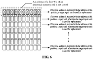
- the fuse address storage module involved in the disclosure may be configured as an electronic programming fuse (E-fuse) module, and configured to store an address of a damaged WL in the normal memory area. It is to be noted that a correspondence between a storage position of the fuse address storage module and a repair unit of the redundant memory area may be configured in advance. For the memory cell of the normal memory area in which the first WL is damaged, the address of the WL cannot be stored at the storage position corresponding to the target repair unit in the fuse address storage module.
- E-fuse electronic programming fuse
- the target repair unit may be used to replace the abnormal memory cell.
- rest repair units other than the target repair unit in the redundant memory area may be used for replacement. There are no limits made by the disclosure on which repair unit is specifically used.
- the target repair unit is used to replace the abnormal memory cell
- the first WL in the target repair unit cannot be used
- only rest WLs of the target repair unit are used to replace corresponding WLs of the abnormal memory cell, and the abnormal memory cell retains the first WL.
- a repair circuit for the rest repair units other than the target repair unit in the redundant memory area may include a comparison circuit 701, an NAND gate and a NOT gate that are cascaded. Similar to the above comparison circuit 301, the comparison circuit 701 is configured to compare the input row address and the fuse address, which will not be repeatedly described thereto.
- each repair unit includes four WLs.
- the RWL0 in the repair unit 0 cannot be used to replace the WL in the normal memory area due to the limitation of the row hammer problem.
- each normal unit includes four WLs.
- the first WL i.e., WL4 in the normal unit 1 is abnormal.
- the repair unit 0 cannot be used for replacement, and any repair unit other than the repair unit 0 may be used to replace the normal unit 1.
- the third WL, i.e., WL14 in the normal unit 3 is abnormal.
- the repair unit 0 may be used for replacement.
- the RWL1, RWL2 and RWL3 in the repair unit 0 are used to replace the WL13, WL14 and WL15 in the normal unit 3, respectively, while the WL12 in the normal unit 3 is used normally.
- any repair unit other than the repair unit 0 may also be used to replace the normal unit 3.
- the disclosure may configure repair priorities for the target repair unit (i.e., the repair unit 0 in the figure) and rest repair units.
- the rest repair units other than the target repair unit in the redundant memory area are not limited in application range, when there is a memory cell to be repaired, whether the target repair unit may be used for repair may be determined preferentially; and if the target repair unit cannot be used for repair, the rest repair units are then used. In this case, the rest repair units having the wider application range are retained, that is, the problem that the abnormal memory cell cannot be repaired due to a fact that the rest repair units are occupied preferentially is avoided.
- the exemplary embodiment of the disclosure may improve the utilization rate of the redundant memory area.
- the disclosure further provides a memory including the above repair circuit.
- the memory 900 may include a redundant memory area 910, a normal memory area 920, a row address receiving end 940 and a repair circuit 930.
- the redundant memory area 910 includes a target repair unit 911 adjacent to the normal memory area.
- the repair circuit 930 is configured to receive a row address from the row address receiving end 940, and control, according to the received row address, the target repair unit 911 to repair an abnormal memory cell in the normal memory area 920; and the specific implementation of the repair circuit 930 is as described above, and will not be repeatedly described.
- the memory 900 may further include a repair circuit for rest repair units other than the target repair unit 911 in the redundant memory area 910.
- the memory 900 may further include a fuse address storage module 950, configured to store an address of a WL corresponding to the abnormal memory cell in the normal memory area as a fuse address.
- the target repair unit 911 may receive the fuse address, to output a repair signal indicating whether to perform a repair operation.
- the memory including the repair circuit according to the exemplary embodiment of the disclosure may improve the utilization rate of the redundant memory area. With comparisons on multiple groups of experiments, the memory according to the exemplary embodiment of the disclosure improves the yield by about 6%.
- the disclosure provides a repair method.
- the repair method is applied to a memory including a normal memory area and a redundant memory area.
- the redundant memory area includes a target repair unit adjacent to the normal memory area.
- the repair method according to the exemplary embodiment of the disclosure may include the following operations.
- a control result is obtained according to signals at a target number of bits from low to high in the row address, where the target number is associated with the number of WLs in the target repair unit.
- the target repair unit in combination with the control result, is controlled to repair an abnormal memory cell in the normal memory area.
- the operation that in combination with the control result, the target repair unit is controlled to repair the abnormal memory cell in the normal memory area in S106 may include that: signals at rest bits other than the target number of bits in the row address are determined; a fuse address corresponding to the abnormal memory cell in the normal memory area is received; the signals at the rest bits are compared with the fuse address bit by bit to obtain multiple comparison results; and according to the multiple comparison results and the control result, the target repair unit is controlled to repair the abnormal memory cell in the normal memory area.
- the abnormal memory cell in a case where the multiple comparison results are that each of the signals at the rest bits is matched with a corresponding bit of the fuse address, if at least one signal among the signals at the target number of bits from low to high in the row address is at a high level, the abnormal memory cell is repaired with the target repair unit; and if the signals at the target number of bits from low to high in the row address are all at a low level, the abnormal memory cell is repaired with a repair unit other than the target repair unit in the redundant memory area.
- the operation that the abnormal memory cell is repaired with the target repair unit may include that: a WL corresponding to the abnormal memory cell is replaced with a WL other than a first WL in the target repair unit; and a first WL of the abnormal memory cell is retained.
- the first WL of the target repair unit is a WL adjacent to the normal memory area.
- the target repair unit adjacent to the normal memory area in the redundant memory area is used to execute the repair operation is determined with information of the row address, that is, when the information of the row address meets the requirements, the target repair unit may be used to replace the abnormal memory cell in the normal memory area. Therefore, compared with the solution in which the target repair unit is not used for repair in some technologies, the exemplary embodiment of the disclosure may improve the utilization rate of the redundant memory area.
Landscapes
- Physics & Mathematics (AREA)
- Engineering & Computer Science (AREA)
- Computer Hardware Design (AREA)
- Computing Systems (AREA)
- General Engineering & Computer Science (AREA)
- Mathematical Physics (AREA)
- For Increasing The Reliability Of Semiconductor Memories (AREA)
- Dram (AREA)
Abstract
Description
- The present application claims priority to
Chinese Patent Application No. 202010111701.8, filed on February 24, 2020 - The disclosure relates to the technical field of semiconductor memories, and more particularly, to a repair circuit, a memory, and a repair method.
- Dynamic Random Access Memory (DRAM) arrays are typically stored to a normal memory area and a redundant memory area. In a case where a memory cell of the normal memory area cannot provide the normal read-write or storage function, a memory cell of the redundant memory area may be used to replace the abnormal memory cell, thereby ensuring normal work of the memory.
- Concerning a row redundancy, due to the row hammer problem, a memory cell closest to the normal memory area in the redundant memory area cannot be used, which causes the loss of resources in the redundant memory area and reduces the utilization rate of the redundant memory area.
- It is to be noted that the information disclosed in the background section is merely for the purpose of enhancing the understanding on the background of the disclosure and thus may include information which does not constitute related art known to those of ordinary skill in the art.
- An objective of the disclosure is to provide a repair circuit, a memory, and a repair method, so as to at least overcome, to some extent, the reduction in the utilization rate of the redundant memory area due to the memory cell closest to the normal memory area in the redundant memory area cannot be used.
- In a first aspect of the disclosure, a repair circuit is provided, which is disposed in a memory including a normal memory area and a redundant memory area, the redundant memory area including a target repair unit immediately adjacent to the normal memory area, and the repair circuit being configured to control the target repair unit to repair an abnormal memory cell in the normal memory area. The repair circuit includes a first control circuit and a repair determination module. The first control circuit is configured to receive signals at a target number of bits from low to high in a row address, process the signals at the target number of bits to obtain a control result, and output the control result. The target number is associated with a number of Word Lines (WLs) in the target repair unit. The repair determination module is connected to an output terminal of the first control circuit, and configured to receive the control result and output, in combination with the control result, a repair signal indicating whether to perform a repair operation.
- Optionally, the repair determination module may include: a comparison circuit, configured to receive signals at rest bits other than the target number of bits in the row address, receive a fuse address, compare the signals at the rest bits with the fuse address bit by bit to obtain multiple comparison results, and output the multiple comparison results; and a second control circuit, connected to the output terminal of the first control circuit and an output terminal of the comparison circuit, and configured to receive the control result and the multiple comparison results, process the control result and the multiple comparison results, and output the repair signal indicating whether to perform the repair operation.
- Optionally, the first control circuit may include: the target number of NOT gates, an input terminal of each of the target number of NOT gates receiving a respective one of the signals at the target number of bits from low to high in the row address; and an NAND gate, an input terminal of the NAND gate being connected to an output terminal of each of the target number of NOT gates, and an output terminal of the NAND gate being connected to the second control circuit, and configured to output the control result.
- Optionally, the comparison circuit may include: multiple XNOR gates, a number of the multiple XNOR gates being the same as the number of the signals at the rest bits other than the target number of bits in the row address, a first input terminal of each of the multiple XNOR gates receiving a respective one of the signals at the rest bits other than the target number of bits in the row address, a second end of the each XNOR gate receiving a corresponding bit of the fuse address, and an output terminal of the each XNOR gate outputting a respective one of the multiple comparison results.
- Optionally, the second control circuit may include: an AND gate, multiple first input terminals of the AND gate being connected to output terminals of the multiple XNOR gates, respectively, a second input terminal of the AND gate being connected to the output terminal of the NAND gate, and an output terminal of the AND gate outputting a repair signal indicating whether to perform the repair operation.
- Optionally, when a number of WLs in the target repair unit is 2n, the target number is n, the n being a positive integer greater than or equal to 2.
- Optionally, when the signals at the target number of bits are all at a low level, the repair determination module outputs a repair signal indicating that no repair operation is to be performed.
- According to a second aspect of the disclosure, a memory is provided, which includes: a normal memory area; a redundant memory area, including a target repair unit immediately adjacent to the normal memory area; a row address receiving end, configured to receive a row address input to the memory; and the above any repair circuit.
- Optionally, the memory may further include: a fuse address storage module, configured to store an address of a WL corresponding to an abnormal memory cell in the normal memory area as a fuse address, where the repair circuit is configured to receive the fuse address, so as to output a repair signal indicating whether to perform a repair operation.
- Optionally, in a storage unit, corresponding to the target repair unit, of the fuse address storage module, an address of a first WL in the abnormal memory cell is not stored.
- According to a third aspect of the disclosure, a repair method is provided, which is applied to a memory including a normal memory area and a redundant memory area, the redundant memory area including a target repair unit immediately adjacent to the normal memory area, and the repair method including that: a row address input to the memory is received; a control result is obtained according to signals at a target number of bits from low to high in the row address, where the target number is associated with a number of WLs in the target repair unit; and in combination with the control result, the target repair unit is controlled to repair an abnormal memory cell in the normal memory area.
- Optionally, the operation that in combination with the control result, the target repair unit is controlled to repair the abnormal memory cell in the normal memory area may include that: signals at rest bits other than the target number of bits in the row address are determined; a fuse address corresponding to the abnormal memory cell in the normal memory area is received; the signals at the rest bits are compared with the fuse address bit by bit to obtain multiple comparison results; and according to the multiple comparison results and the control result, the target repair unit is controlled to repair the abnormal memory cell in the normal memory area.
- Optionally, when the multiple comparison results are that each of the signals at the rest bits is matched with a corresponding bit of the fuse address, the operation that according to the multiple comparison results and the control result, the target repair unit is controlled to repair the abnormal memory cell in the normal memory area may include that: when at least one signal among the signals at the target number of bits from low to high in the row address is at a high level, the abnormal memory cell is repaired with the target repair unit; and when the signals at the target number of bits from low to high in the row address are all at a low level, the abnormal memory cell is repaired with a repair unit other than the target repair unit in the redundant memory area.
- Optionally, the operation that the abnormal memory cell is repaired with the target repair unit may include that: a WL corresponding to the abnormal memory cell is replaced with a rest WL other than a first WL in the target repair unit; and a first WL of the abnormal memory cell is retained, where the first WL of the target repair unit is a WL adjacent to the normal memory area.
- In the technical solutions provided by some embodiments of the disclosure, the repair circuit includes a first control circuit and a repair determination module, the first control circuit is configured to receive signals at the target number of bits from low to high in a row address and output a control result, and the repair determination module outputs, in combination with the control result, a repair signal indicating whether to perform a repair operation. Whether the target repair unit immediately adjacent to the normal memory area in the redundant memory area is used to perform the repair operation is determined with information of the row address, that is, when the information of the row address meets the requirements, the target repair unit may be used to replace the abnormal memory cell. Therefore, compared with the solution in which the target repair unit is not used for repair in some technologies, the exemplary embodiment of the disclosure may improve the utilization rate of the redundant memory area.
- It is to be understood that the above general descriptions and detailed descriptions below are only exemplary and explanatory and not intended to limit the disclosure.
- The accompanying drawings, which are incorporated in and constitute a part of this specification, illustrate embodiments consistent with the disclosure and, together with the description, serve to explain the principles of the disclosure. It is apparent that the accompanying drawings in the description below are merely some of the embodiments of the disclosure, based on which other drawings may be obtained by a person of ordinary skill in the art without any creative effort. In the drawings:
-
FIG. 1 illustrates a schematic diagram of a memory array according to an exemplary embodiment of the disclosure. -
FIG. 2 illustrates a schematic diagram of a repair circuit according to an exemplary embodiment of the disclosure. -
FIG. 3 illustrates a schematic diagram of a repair determination module including a comparison circuit and a second control circuit in a repair circuit according to an exemplary embodiment of the disclosure. -
FIG. 4 illustrates a schematic diagram of a specific form of a first control circuit and a second control circuit according to some embodiments of the disclosure. -
FIG. 5 illustrates a schematic diagram of a comparison circuit according to some embodiments of the disclosure. -
FIG. 6 illustrates a schematic diagram for describing a fuse address storage module according to some embodiments of the disclosure. -
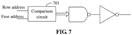
FIG. 7 illustrates a schematic diagram of a repair circuit applied to repair units other than a target repair unit in a redundant memory area according to some embodiments of the disclosure. -
FIG. 8 illustrates a schematic diagram of a manner for repairing a memory cell according to an embodiment of the disclosure. -
FIG. 9 illustrates a schematic diagram of a memory according to an exemplary embodiment of the disclosure. -
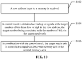
FIG. 10 illustrates a flowchart of a repair method according to an exemplary embodiment of the disclosure. - Exemplary embodiments will now be described more fully with reference to the accompanying drawings. However, the exemplary embodiments may be implemented in various forms and should not be understood as being limited to the examples set forth herein; rather, these embodiments are provided to make the disclosure more thorough and complete, and to fully convey the concepts of the exemplary embodiments to those skilled in the art. The features, structures or characteristics described herein may be combined in one or more embodiments in any suitable manner. In the following description, numerous specific details are provided to offer a thorough understanding on the embodiments of the disclosure. However, it will be recognized by those skilled in the art that the technical solution of the disclosure may be practiced without one or more of the specific details, or that other methods, components, devices, steps, and the like may be employed. In other instances, well-known technical solutions are not shown or described in detail to avoid obscuring aspects of the disclosure.
- In addition, the drawings are merely schematic representations of the disclosure and are not necessarily drawn to scale. The same reference numerals in the drawings denote the same or similar parts, and repetitive description thereof will be omitted.
- In manufacture of the DRAM, the increasingly higher accuracy and the increasingly smaller size require that more structures are integrated on one chip. In this case, interference easily occurs between memory cells, and the row hammer phenomenon may occur.
- The row hammer may be understood as that when one Word Line (WL) is intensively accessed (for example, repeated read and write operations or maliciously attacked), charges stored in an adjacent memory cell may be affected to change from 0 to 1 or from 1 to 0, and such a random flipping will cause errors in the storage data. It is easily understood by those skilled in the art that the WL used herein is usually used for controlling an on-off state of a memory cell. For example, when the WL is at a high level, the corresponding memory cell is on; and when the WL is at a low level, the corresponding memory cell is off.
- In addition, with regard to the DRAM repair solution, when a memory cell in the normal memory area is abnormal, a repair unit in the redundant memory area may be used for repair. In view that the number of control circuits is restricted and multiple continuous WLs may be damaged at the same time in actual damage, the usual repair process is to use multiple continuous WLs in the redundant memory area to replace the abnormal WLs at the same time. The multiple continuous WLs correspond to one repair unit.
- In some technologies, during configuring the repair solution of the memory, a repair unit adjacent to the normal memory area in the redundant memory area is not used. Hence, the influence of the adjacent repair unit on the normal memory area is avoided, and the row hammer problem is solved to some extent.
- As illustrated in
FIG. 1 , the memory in the exemplary embodiment of the disclosure may include anormal memory area 11 and aredundant memory area 10. Thenormal memory area 11 includes N+1 WLs in total such as WL0, WL1, WL2, ..., WLN. Theredundant memory area 10 includes M+1 WLs in total such as RWL0, RWL1, RWL2, ..., RWLM. The M is usually less than N. - In the
redundant memory area 10, four WLs may be used to form one repair unit. For example, therepair unit 0 includes RWL0, RWL1, RWL2 and RWL3. If two continuous WLs in thenormal memory area 11 are damaged, four WLs of the repair unit in the redundant memory area can be used to replace the two damaged WLs and the two adjacent WLs (that is, four WLs in total are replaced). Or, if two continuous WLs in thenormal memory area 11 are damaged, a normal unit(s) corresponding to the two WLs may be determined, and all WLs of the normal unit(s) corresponding to the two WLs are replaced with the repair unit as the unit. - However, it is further found by the inventor that typically only the first WL in the repair unit adjacent to the normal memory area in the redundant memory area has an influence on the normal memory area; and corresponding to
FIG. 1 , that is, the RWL0 of therepair unit 0 in theredundant memory area 10 usually has the row hammer problem. In a case where therepair unit 0 further includes RWL1, RWL2 and RWL3, these three WLs also do not participate in the repair operation. Therefore, the available resources are wasted. - In view of this, in some embodiments of the disclosure, a solution in which rest WLs other than the WL adjacent to the normal memory area in the
above repair unit 0 can participate in the repair process is proposed, to improve the utilization rate of the redundant memory area. - Specifically, an exemplary embodiment of the disclosure provides a repair circuit. The repair circuit is disposed in a memory. The memory may be, for example, the DRAM. The memory may further be a Double Data Rate Fourth Synchronous Dynamic Random Access Memory (DDR4 SDRAM). There are no limits made on the type of the memory in the disclosure.
- The memory may include a normal memory area and a redundant memory area. The redundant memory area is configured to repair an abnormity when a memory cell in the normal memory area is abnormal. The abnormity of the memory cell may refer to a case where a normal read-write service cannot be provided due to a short circuit or an open circuit in manufacture or later use. The normal memory area and the redundant memory area are exemplarily illustrated in
FIG. 1 , and are not repeatedly described. - In the exemplary embodiment of the disclosure, a repair unit immediately adjacent to the normal memory area in the redundant memory area is referred to as a target repair unit. In the exemplary example of
FIG. 1 , the target repair unit corresponds to therepair unit 0. - The repair circuit provided by the exemplary embodiment of the disclosure may be configured to selectively control the target repair unit to repair the abnormal memory cell in the normal memory area. Referring to
FIG. 2 , the repair circuit may include afirst control circuit 21 and arepair determination module 22. - The
first control circuit 21 may be configured to receive signals at the target number of bits from low to high in an input row address. For example, in a case where the row address is 12 bits and is characterized as <11:0>, being from low to high refers to from the 0th bit to the 11th bit. - In addition, the target number is associated with the number of WLs in the target repair unit. If the number of WLs in the target repair unit is 2n, the target number is n, the n being a positive integer greater than or equal to 2. For example, in a case where the repair unit illustrated in
FIG. 1 includes 4 WLs, the target number is 2. However, it is to be understood that for different memories, the repair unit may include 8 or 16 WLs, and the target number is 3 or 4, respectively. - After receiving the signals at the target number of bits from low to high in the row address, the
first control circuit 21 may process these signals to obtain a control result and output the control result. The control result in the embodiment of the disclosure may be a high-level or low-level signal. - The
repair determination module 22 is connected to an output terminal of thefirst control circuit 21, and configured to receive the control result from thefirst control circuit 21 and output, in combination with the control result, a repair signal indicating whether to perform a repair operation. That is, therepair determination module 22 may output, in combination with one control result, a repair signal indicating that the repair operation is to be performed, so as to control the target repair unit to repair the abnormal memory cell in the normal memory area. Alternatively, therepair determination module 22 may output, in combination with another control result, a repair signal indicating that no repair operation is to be performed. In this case, a rest repair unit other than the target repair unit in the redundant memory area may be used to repair the abnormal memory cell in the normal memory area. - It is to be noted that in a case where the signals at the target number of bits are all at the low level, the following may be obtained: the
repair determination module 22 outputs the repair signal of not executing the repair operation. - In a case where at least one of the signals at the target number of bits is at the high level, a result on whether the row address is matched with a fuse address may further be combined to determine whether to use the target repair unit to repair the abnormal memory cell in the normal memory area.
- Specifically, when the row address is matched with the fuse address, that is, signals at bits corresponding to the row address and the fuse address are the same, the target repair unit is used to repair the abnormal memory cell in the normal memory area.
- When the row address is not matched with the fuse address, no processing is performed.
- Referring to
FIG. 3 , therepair determination module 22 further includes acomparison circuit 301 and asecond control circuit 302. - The
comparison circuit 301 is configured to receive signals at rest bits other than the target number of bits in the row address. Still with the case where the row address is 12 bits and is characterized by <11:0> as an example, if the repair unit includes 4 WLs, that is, the target number is 2, the signals at the rest bits other than the target number of bits in the row address are <11:2>. The signals at the 0th bit and the 1st bit are the input of thefirst control circuit 21. - In addition, the
comparison circuit 301 is further configured to receive the fuse address, compare the signals at the rest bits with the fuse address bit by bit to obtain multiple comparison results, and output the comparison results. For example, in a case where each of the row address and the fuse address is 12 bits, < 11:2> signals of the row address are compared with <11:2> signals of the fuse address bit by bit. For example, the 2nd bit of the row address is compared with the 2nd bit of the fuse address, the 3rd bit of the row address is compared with the 3rd bit of the fuse address, and the like. In this case, thecomparison circuit 301 mayoutput 10 comparison results. It is to be understood that the comparison result in the embodiment of the disclosure may also be a high-level or low-level signal. Specifically, in a case where the signals at the corresponding bits are the same, the comparison result is the high level; and in a case where the signals at the corresponding bits are different, the comparison result is the low level. - The
second control circuit 302 is connected to an output terminal of thefirst control circuit 21 and an output terminal of thecomparison circuit 301. Thesecond control circuit 302 is configured to receive the above control result and multiple comparison results, process the control result and multiple comparison results, and output a repair signal indicating whether to perform a repair operation. - According to some embodiments of the disclosure, the
first control circuit 21 may include the target number of NOT gates and an NAND gate. - Specifically, an input terminal of each NOT gate receives a respective one of the signals at the target number of bits from low to high in the row address. An input terminal of the NAND gate is connected to an output terminal of each NOT gate, and an output terminal of the NAND gate is connected to the
second control circuit 302, and configured to output the above control result to thesecond control circuit 301. - The
comparison circuit 301 includes multiple XNOR gates, and the number of the XNOR gates is the same as the number of the signals at the rest bits other than the target number of bits in the row address. Each XNOR gate includes a first input terminal and a second input terminal, the first input terminal receives a respective one of the signals at the rest bits other than the target number of bits in the row address, the second input terminal receives a corresponding bit of the fuse address, and an output terminal of each XNOR outputs a responsive one of the multiple comparison results. - The
second control circuit 302 includes an AND gate; the AND gate includes multiple first input terminals and a second input terminal; and the number of the first input terminals is the same as the number of the XNOR gates in thecomparison circuit 301. Each first input terminal is connected to an output terminal of a respective XNOR gate, and the second input terminal is connected to the output terminal of the NAND gate of thefirst control circuit 21. The output terminal of the AND gate outputs a repair signal indicating whether to perform a repair operation. - Referring to
FIG. 4 , with a case where the repair unit includes 4 WLs as an example, the specific forms of thefirst control circuit 21 and thesecond control circuit 302 will be described below. - Referring to
FIG. 4 , thefirst control circuit 21 includes two NOT gates that respectively receive the row address <0> and the row address <1>. Outputs of the two NOT gates are used as the input of the NAND gate, and the output of the NAND gate is the control result described above. - Due to limitations of manufacture procedure and other restraints of the process, the AND gate of the
second control circuit 302 is usually configured as a cascaded form of one NAND gate and one NOT gate. The input terminal of the NAND respectively receives each comparison result output by thecomparison circuit 301 and the control result output by thefirst control circuit 21. - In a case where the row address has N+1 bits in total, the signal received by the
comparison circuit 301 is the row address <N:2> and the fuse address <N:2>. -
FIG. 5 illustrates a structural schematic diagram of thecomparison circuit 301. Referring toFIG. 5 , the input of each XNOR gate is one bit of signal in the row address and the signal at the corresponding bit in the fuse address. - In addition, the output of each XNOR gate may further be input to one AND gate (not shown); and the output of the AND gate is used as the output of the
comparison circuit 301 to forward to thesecond control circuit 302. - It is easily understood by those skilled in the art that in a case where there are multiple fuse addresses, the input row address is respectively compared with each fuse address.
- For the fuse address input to the comparison circuit, the fuse address storage module of the disclosure will be exemplarily described below with reference to
FIG. 6 . - The fuse address storage module involved in the disclosure may be configured as an electronic programming fuse (E-fuse) module, and configured to store an address of a damaged WL in the normal memory area. It is to be noted that a correspondence between a storage position of the fuse address storage module and a repair unit of the redundant memory area may be configured in advance. For the memory cell of the normal memory area in which the first WL is damaged, the address of the WL cannot be stored at the storage position corresponding to the target repair unit in the fuse address storage module.
- Referring to
FIG. 6 , for the storage position where the address of the first WL of the abnormal memory cell is not stored, if the row address is matched with the address stored at this position, the target repair unit may be used to replace the abnormal memory cell. For other memory addresses, rest repair units other than the target repair unit in the redundant memory area may be used for replacement. There are no limits made by the disclosure on which repair unit is specifically used. - In addition, in a case where the target repair unit is used to replace the abnormal memory cell, as the first WL in the target repair unit cannot be used, only rest WLs of the target repair unit are used to replace corresponding WLs of the abnormal memory cell, and the abnormal memory cell retains the first WL.
- Referring to
FIG. 7 , a repair circuit for the rest repair units other than the target repair unit in the redundant memory area may include acomparison circuit 701, an NAND gate and a NOT gate that are cascaded. Similar to theabove comparison circuit 301, thecomparison circuit 701 is configured to compare the input row address and the fuse address, which will not be repeatedly described thereto. - A manner for repairing the memory cell in an embodiment of the disclosure will be described below with reference to
FIG. 8 . - In the
redundant memory area 80, each repair unit includes four WLs. The RWL0 in therepair unit 0 cannot be used to replace the WL in the normal memory area due to the limitation of the row hammer problem. In thenormal memory area 81, each normal unit includes four WLs. - As illustrated in
FIG. 8 , the first WL, i.e., WL4 in thenormal unit 1 is abnormal. In this case, based on the repair solution in the exemplary embodiment of the disclosure, as the first WL is damaged, therepair unit 0 cannot be used for replacement, and any repair unit other than therepair unit 0 may be used to replace thenormal unit 1. - The third WL, i.e., WL14 in the
normal unit 3 is abnormal. In this case, based on the repair solution in the exemplary embodiment of the disclosure, therepair unit 0 may be used for replacement. Specifically, the RWL1, RWL2 and RWL3 in therepair unit 0 are used to replace the WL13, WL14 and WL15 in thenormal unit 3, respectively, while the WL12 in thenormal unit 3 is used normally. - It is to be noted that when the third WL, i.e., WL14 in the
normal unit 3 is abnormal, any repair unit other than therepair unit 0 may also be used to replace thenormal unit 3. - The disclosure may configure repair priorities for the target repair unit (i.e., the
repair unit 0 in the figure) and rest repair units. As the rest repair units other than the target repair unit in the redundant memory area are not limited in application range, when there is a memory cell to be repaired, whether the target repair unit may be used for repair may be determined preferentially; and if the target repair unit cannot be used for repair, the rest repair units are then used. In this case, the rest repair units having the wider application range are retained, that is, the problem that the abnormal memory cell cannot be repaired due to a fact that the rest repair units are occupied preferentially is avoided. - Based on the repair circuit in the exemplary embodiment of the disclosure, whether the target repair unit adjacent to the normal memory area in the redundant memory area is used for performing the repair operation is determined with information of the row address, that is, when the information of the row address meets the requirements, the target repair unit may be used to replace the abnormal memory cell. Therefore, compared with the solution in which the target repair unit is not used for repair in some technologies, the exemplary embodiment of the disclosure may improve the utilization rate of the redundant memory area.
- Further, the disclosure further provides a memory including the above repair circuit.
- Referring to
FIG. 9 , thememory 900 may include aredundant memory area 910, anormal memory area 920, a rowaddress receiving end 940 and arepair circuit 930. - The
redundant memory area 910 includes atarget repair unit 911 adjacent to the normal memory area. Therepair circuit 930 is configured to receive a row address from the rowaddress receiving end 940, and control, according to the received row address, thetarget repair unit 911 to repair an abnormal memory cell in thenormal memory area 920; and the specific implementation of therepair circuit 930 is as described above, and will not be repeatedly described. - It is to be noted that though not illustrated, the
memory 900 may further include a repair circuit for rest repair units other than thetarget repair unit 911 in theredundant memory area 910. - In addition, the
memory 900 may further include a fuseaddress storage module 950, configured to store an address of a WL corresponding to the abnormal memory cell in the normal memory area as a fuse address. Thetarget repair unit 911 may receive the fuse address, to output a repair signal indicating whether to perform a repair operation. - In a storage unit, corresponding to the target repair unit, of the fuse
address storage module 950, an address of a first WL in the abnormal memory cell is not stored. - Compared with a memory in which the target repair unit is not used for repair in some technologies, the memory including the repair circuit according to the exemplary embodiment of the disclosure may improve the utilization rate of the redundant memory area. With comparisons on multiple groups of experiments, the memory according to the exemplary embodiment of the disclosure improves the yield by about 6%.
- Further, the disclosure provides a repair method. The repair method is applied to a memory including a normal memory area and a redundant memory area. The redundant memory area includes a target repair unit adjacent to the normal memory area.
- Referring to
FIG. 10 , the repair method according to the exemplary embodiment of the disclosure may include the following operations. - In S102, a row address input to a memory is received.
- In S104, a control result is obtained according to signals at a target number of bits from low to high in the row address, where the target number is associated with the number of WLs in the target repair unit.
- In S106, in combination with the control result, the target repair unit is controlled to repair an abnormal memory cell in the normal memory area.
- According to the exemplary embodiment of the disclosure, the operation that in combination with the control result, the target repair unit is controlled to repair the abnormal memory cell in the normal memory area in S106 may include that: signals at rest bits other than the target number of bits in the row address are determined; a fuse address corresponding to the abnormal memory cell in the normal memory area is received; the signals at the rest bits are compared with the fuse address bit by bit to obtain multiple comparison results; and according to the multiple comparison results and the control result, the target repair unit is controlled to repair the abnormal memory cell in the normal memory area.
- According to the exemplary embodiment of the disclosure, in a case where the multiple comparison results are that each of the signals at the rest bits is matched with a corresponding bit of the fuse address, if at least one signal among the signals at the target number of bits from low to high in the row address is at a high level, the abnormal memory cell is repaired with the target repair unit; and if the signals at the target number of bits from low to high in the row address are all at a low level, the abnormal memory cell is repaired with a repair unit other than the target repair unit in the redundant memory area.
- According to the exemplary embodiment of the disclosure, the operation that the abnormal memory cell is repaired with the target repair unit may include that: a WL corresponding to the abnormal memory cell is replaced with a WL other than a first WL in the target repair unit; and a first WL of the abnormal memory cell is retained. The first WL of the target repair unit is a WL adjacent to the normal memory area.
- Based on the repair method in the exemplary embodiment of the disclosure, whether the target repair unit adjacent to the normal memory area in the redundant memory area is used to execute the repair operation is determined with information of the row address, that is, when the information of the row address meets the requirements, the target repair unit may be used to replace the abnormal memory cell in the normal memory area. Therefore, compared with the solution in which the target repair unit is not used for repair in some technologies, the exemplary embodiment of the disclosure may improve the utilization rate of the redundant memory area.
- Other embodiments of the disclosure will be apparent to those skilled in the art from consideration of the specification and practice of the disclosure disclosed herein. This application is intended to cover any variations, uses, or adaptations of the disclosure following the general principles thereof and including such departures from the disclosure as come within known or customary practice in the art. The specification and embodiments are considered as exemplary only, with a true scope and spirit of the disclosure being indicated by the claims.
- It will be appreciated that the disclosure is not limited to the exact construction that has been described above and illustrated in the accompanying drawings, and that various modifications and changes may be made without departing from the scope thereof. The scope of the disclosure only be limited by the appended claims.
Claims (14)
- A repair circuit, disposed in a memory comprising a normal memory area and a redundant memory area, wherein the redundant memory area comprises a target repair unit immediately adjacent to the normal memory area, the repair circuit is configured to control the target repair unit to repair an abnormal memory cell in the normal memory area, and the repair circuit comprises:a first control circuit, configured to receive signals at a target number of bits from low to high in a row address, process the signals at the target number of bits to obtain a control result, and output the control result, wherein the target number is associated with a number of Word Lines (WLs) in the target repair unit; anda repair determination module, connected to an output terminal of the first control circuit, and configured to receive the control result and output, in combination with the control result, a repair signal indicating whether to perform a repair operation.
- The repair circuit of claim 1, wherein the repair determination module comprises:a comparison circuit, configured to receive signals at rest bits other than the target number of bits in the row address, receive a fuse address, compare the signals at the rest bits with the fuse address bit by bit to obtain a plurality of comparison results, and output the plurality of comparison results; anda second control circuit, connected to the output terminal of the first control circuit and an output terminal of the comparison circuit, and configured to receive the control result and the plurality of comparison results, process the control result and the plurality of comparison results, and output the repair signal indicating whether to perform the repair operation.
- The repair circuit of claim 2, wherein the first control circuit comprises:the target number of NOT gates, an input terminal of each of the target number of NOT gates receiving a respective one of the signals at the target number of bits from low to high in the row address; andan NAND gate, an input terminal of the NAND gate being connected to an output terminal of each of the target number of NOT gates, and an output terminal of the NAND gate being connected to the second control circuit, and configured to output the control result.
- The repair circuit of claim 3, wherein the comparison circuit comprises:
a plurality of XNOR gates, wherein a number of the plurality of XNOR gates is the same as a number of the signals at the rest bits other than the target number of bits in the row address, a first input terminal of each of the plurality of XNOR gates receives a respective one of the signals at the rest bits other than the target number of bits in the row address, a second input terminal of the each XNOR gate receives a corresponding bit of the fuse address, and an output terminal of the each XNOR gate outputs a responsive one of the plurality of comparison results. - The repair circuit of claim 4, wherein the second control circuit comprises:
an AND gate, wherein a plurality of first input terminals of the AND gate are connected to output terminals of the plurality of XNOR gates, respectively, a second input terminal of the AND gate is connected to the output terminal of the NAND gate, and an output terminal of the AND gate outputs a repair signal indicating whether to perform the repair operation. - The repair circuit of claim 1, wherein when a number of WLs in the target repair unit is 2n, the target number is n, the n being a positive integer greater than or equal to 2.
- The repair circuit of any one of claims 1 to 6, wherein when the signals at the target number of bits are all at a low level, the repair determination module outputs a repair signal indicating that no repair operation is to be performed.
- A memory, comprising:a normal memory area;a redundant memory area, comprising a target repair unit immediately adjacent to the normal memory area;a row address receiving end, configured to receive a row address input to the memory; andthe repair circuit of any one of claims 1 to 7.
- The memory of claim 8, further comprising:a fuse address storage module, configured to store an address of a Word Line (WL) corresponding to an abnormal memory cell in the normal memory area as a fuse address,wherein the repair circuit is configured to receive the fuse address, to output a repair signal indicating whether to perform a repair operation.
- The memory of claim 9, wherein in a storage unit, corresponding to the target repair unit, of the fuse address storage module, an address of a first WL in the abnormal memory cell is not stored.
- A repair method, applied to a memory comprising a normal memory area and a redundant memory area, wherein the redundant memory area comprises a target repair unit immediately adjacent to the normal memory area, and the repair method comprises:receiving a row address input to the memory;obtaining a control result according to signals at a target number of bits from low to high in the row address, wherein the target number is associated with a number of Word Lines (WLs) in the target repair unit; andcontrolling, in combination with the control result, the target repair unit to repair an abnormal memory cell in the normal memory area.
- The repair method of claim 11, wherein controlling, in combination with the control result, the target repair unit to repair the abnormal memory cell in the normal memory area comprises:determining signals at rest bits other than the target number of bits in the row address;receiving a fuse address corresponding to the abnormal memory cell in the normal memory area;comparing the signals at the rest bits with the fuse address bit by bit to obtain a plurality of comparison results; andcontrolling, according to the plurality of comparison results and the control result, the target repair unit to repair the abnormal memory cell in the normal memory area.
- The repair method of claim 12, wherein when the plurality of comparison results are that each of the signals at the rest bits is matched with a corresponding bit of the fuse address, controlling, according to the plurality of comparison results and the control result, the target repair unit to repair the abnormal memory cell in the normal memory area comprises:repairing, when at least one signal among the signals at the target number of bits from low to high in the row address is at a high level, the abnormal memory cell with the target repair unit; andrepairing, when the signals at the target number of bits from low to high in the row address are all at a low level, the abnormal memory cell with a repair unit other than the target repair unit in the redundant memory area.
- The repair method of claim 13, wherein repairing the abnormal memory cell with the target repair unit comprises:replacing a WL corresponding to the abnormal memory cell with a rest WL other than a first WL in the target repair unit; andretaining a first WL of the abnormal memory cell,wherein the first WL of the target repair unit is a WL adjacent to the normal memory area.
Applications Claiming Priority (2)
| Application Number | Priority Date | Filing Date | Title |
|---|---|---|---|
| CN202010111701.8A CN113299336B (en) | 2020-02-24 | 2020-02-24 | Repair circuit, memory and repair method |
| PCT/CN2021/073269 WO2021169692A1 (en) | 2020-02-24 | 2021-01-22 | Repair circuit, memory, and repair method |
Publications (3)
| Publication Number | Publication Date |
|---|---|
| EP3933841A1 true EP3933841A1 (en) | 2022-01-05 |
| EP3933841A4 EP3933841A4 (en) | 2022-05-25 |
| EP3933841B1 EP3933841B1 (en) | 2023-12-27 |
Family
ID=77317819
Family Applications (1)
| Application Number | Title | Priority Date | Filing Date |
|---|---|---|---|
| EP21761667.1A Active EP3933841B1 (en) | 2020-02-24 | 2021-01-22 | Repair circuit, memory, and repair method |
Country Status (4)
| Country | Link |
|---|---|
| US (1) | US11972828B2 (en) |
| EP (1) | EP3933841B1 (en) |
| CN (1) | CN113299336B (en) |
| WO (1) | WO2021169692A1 (en) |
Families Citing this family (5)
| Publication number | Priority date | Publication date | Assignee | Title |
|---|---|---|---|---|
| EP4030436B1 (en) * | 2020-10-20 | 2024-05-29 | Changxin Memory Technologies, Inc. | Repair circuit and memory |
| KR102924776B1 (en) * | 2021-10-12 | 2026-02-09 | 삼성전자주식회사 | Semiconductor memory device and method of operating the same |
| US20230205872A1 (en) * | 2021-12-23 | 2023-06-29 | Advanced Micro Devices, Inc. | Method and apparatus to address row hammer attacks at a host processor |
| CN117423376A (en) * | 2022-07-11 | 2024-01-19 | 华为技术有限公司 | Storage control circuit, memory, memory repair method and electronic equipment |
| CN121171308A (en) * | 2025-11-18 | 2025-12-19 | 极芯拓方技术(上海)有限公司 | Memory and electronic equipment |
Family Cites Families (25)
| Publication number | Priority date | Publication date | Assignee | Title |
|---|---|---|---|---|
| KR0172844B1 (en) * | 1995-12-11 | 1999-03-30 | 문정환 | Repair circuit of semiconductor memory |
| JP2002501654A (en) | 1997-05-30 | 2002-01-15 | ミクロン テクノロジー,インコーポレイテッド | 256Meg dynamic random access memory |
| US6314030B1 (en) * | 2000-06-14 | 2001-11-06 | Micron Technology, Inc. | Semiconductor memory having segmented row repair |
| US6967896B2 (en) * | 2003-01-30 | 2005-11-22 | Saifun Semiconductors Ltd | Address scramble |
| US7006393B2 (en) * | 2004-06-07 | 2006-02-28 | Micron Technology, Inc. | Method and apparatus for semiconductor device repair with reduced number of programmable elements |
| US7116590B2 (en) * | 2004-08-23 | 2006-10-03 | Micron Technology, Inc. | Memory address repair without enable fuses |
| KR20060029319A (en) * | 2004-10-01 | 2006-04-06 | 삼성전자주식회사 | Semiconductor memory device |
| JP5612244B2 (en) * | 2007-10-30 | 2014-10-22 | ピーエスフォー ルクスコ エスエイアールエルPS4 Luxco S.a.r.l. | Semiconductor device and refresh method |
| KR101475346B1 (en) * | 2008-07-02 | 2014-12-23 | 삼성전자주식회사 | Develop level clipping circuit for clipping a develop level of a bitline pair, column path circuit including the same, and multi-port semiconductor memory device |
| JP5123140B2 (en) * | 2008-11-12 | 2013-01-16 | 株式会社東芝 | Ferroelectric memory |
| KR101932664B1 (en) * | 2012-08-27 | 2018-12-26 | 삼성전자 주식회사 | Semiconductor memory device and system having redundancy Cells |
| JP2015219938A (en) | 2014-05-21 | 2015-12-07 | マイクロン テクノロジー, インク. | Semiconductor device |
| KR20160004585A (en) * | 2014-07-03 | 2016-01-13 | 에스케이하이닉스 주식회사 | Semiconductor memory device and operating method thereof |
| KR20160011021A (en) * | 2014-07-21 | 2016-01-29 | 에스케이하이닉스 주식회사 | Memory device |
| KR20180033670A (en) * | 2016-09-26 | 2018-04-04 | 에스케이하이닉스 주식회사 | Semiconductor memory device and operating method thereof |
| KR102686059B1 (en) * | 2016-10-26 | 2024-07-18 | 에스케이하이닉스 주식회사 | Semiconductor device |
| KR102713402B1 (en) * | 2016-12-13 | 2024-10-07 | 에스케이하이닉스 주식회사 | Semiconductor device and semiconductor system including the same |
| US10514983B2 (en) * | 2017-04-26 | 2019-12-24 | Micron Technology, Inc. | Memory apparatus with redundancy array |
| KR102401882B1 (en) | 2017-12-04 | 2022-05-26 | 에스케이하이닉스 주식회사 | Memory system and memory maintenance method for improving memory reliability |
| KR102468764B1 (en) * | 2017-12-19 | 2022-11-18 | 에스케이하이닉스 주식회사 | Semiconductor apparatus |
| US10971247B2 (en) * | 2018-03-29 | 2021-04-06 | Samsung Electronics Co., Ltd. | Semiconductor memory devices, memory systems, and methods of operating semiconductor memory devices |
| CN108447520B (en) * | 2018-05-03 | 2023-10-13 | 长鑫存储技术有限公司 | Memory circuit device and memory detection method |
| US11152050B2 (en) * | 2018-06-19 | 2021-10-19 | Micron Technology, Inc. | Apparatuses and methods for multiple row hammer refresh address sequences |
| JP6804493B2 (en) * | 2018-07-19 | 2020-12-23 | 華邦電子股▲ふん▼有限公司Winbond Electronics Corp. | Memory device and memory peripheral circuit |
| CN210925503U (en) * | 2020-02-24 | 2020-07-03 | 长鑫存储技术(上海)有限公司 | Repair circuit and memory |
-
2020
- 2020-02-24 CN CN202010111701.8A patent/CN113299336B/en active Active
-
2021
- 2021-01-22 EP EP21761667.1A patent/EP3933841B1/en active Active
- 2021-01-22 WO PCT/CN2021/073269 patent/WO2021169692A1/en not_active Ceased
- 2021-09-17 US US17/477,769 patent/US11972828B2/en active Active
Also Published As
| Publication number | Publication date |
|---|---|
| CN113299336A (en) | 2021-08-24 |
| WO2021169692A1 (en) | 2021-09-02 |
| CN113299336B (en) | 2024-06-28 |
| US20220005544A1 (en) | 2022-01-06 |
| EP3933841A4 (en) | 2022-05-25 |
| EP3933841B1 (en) | 2023-12-27 |
| US11972828B2 (en) | 2024-04-30 |
Similar Documents
| Publication | Publication Date | Title |
|---|---|---|
| US11972828B2 (en) | Repair circuit, memory, and repair method | |
| US10332614B2 (en) | Methods, apparatus, and systems to repair memory | |
| US10541045B2 (en) | Semiconductor apparatus related to the repairing of a redundancy region | |
| CN210925503U (en) | Repair circuit and memory | |
| JPH05166396A (en) | Semiconductor memory device | |
| US8913451B2 (en) | Memory device and test method thereof | |
| US20010053101A1 (en) | Semiconductor memory having segmented row repair | |
| US11621050B2 (en) | Semiconductor memory devices and repair methods of the semiconductor memory devices | |
| US9583161B1 (en) | Repair circuit, memory apparatus using the same and operating method thereof | |
| US8867288B2 (en) | Memory device and test method thereof | |
| US9852814B1 (en) | Rupture control device and semiconductor device to improve yield | |
| US10802759B2 (en) | Memory system including memory device and memory controller, and operating method thereof | |
| US10726939B2 (en) | Memory devices having spare column remap storages | |
| US20120269018A1 (en) | Memory system having memory and memory controller and operation method thereof | |
| US20140181456A1 (en) | Memory, memory controller, memory system including the memory and the memory controller, and operating method of the memory system | |
| US10198201B2 (en) | Semiconductor apparatus, memory system and repair method thereof | |
| US7359260B2 (en) | Repair of memory cells | |
| US11972829B2 (en) | Semiconductor apparatus | |
| US6331963B1 (en) | Semiconductor memory device and layout method thereof | |
| US12288588B2 (en) | Memory, memory system and operation method of memory | |
| KR102900763B1 (en) | Repair circuit and memory device including the same | |
| CN111599392B (en) | Memory and how to operate it | |
| CN120388599B (en) | Repairing method and repairing system for storage device | |
| US6754113B2 (en) | Topography correction for testing of redundant array elements | |
| US8422321B2 (en) | Semiconductor memory device having regular area and spare area |
Legal Events
| Date | Code | Title | Description |
|---|---|---|---|
| STAA | Information on the status of an ep patent application or granted ep patent |
Free format text: STATUS: THE INTERNATIONAL PUBLICATION HAS BEEN MADE |
|
| PUAI | Public reference made under article 153(3) epc to a published international application that has entered the european phase |
Free format text: ORIGINAL CODE: 0009012 |
|
| STAA | Information on the status of an ep patent application or granted ep patent |
Free format text: STATUS: REQUEST FOR EXAMINATION WAS MADE |
|
| 17P | Request for examination filed |
Effective date: 20210930 |
|
| AK | Designated contracting states |
Kind code of ref document: A1 Designated state(s): AL AT BE BG CH CY CZ DE DK EE ES FI FR GB GR HR HU IE IS IT LI LT LU LV MC MK MT NL NO PL PT RO RS SE SI SK SM TR |
|
| REG | Reference to a national code |
Ref country code: DE Ref legal event code: R079 Free format text: PREVIOUS MAIN CLASS: G11C0029440000 Ipc: G11C0029000000 Ref document number: 602021008145 Country of ref document: DE |
|
| A4 | Supplementary search report drawn up and despatched |
Effective date: 20220428 |
|
| RIC1 | Information provided on ipc code assigned before grant |
Ipc: G11C 29/04 20060101ALN20220421BHEP Ipc: G11C 29/52 20060101ALI20220421BHEP Ipc: G11C 29/44 20060101ALI20220421BHEP Ipc: G11C 29/00 20060101AFI20220421BHEP |
|
| STAA | Information on the status of an ep patent application or granted ep patent |
Free format text: STATUS: EXAMINATION IS IN PROGRESS |
|
| 17Q | First examination report despatched |
Effective date: 20230131 |
|
| DAV | Request for validation of the european patent (deleted) | ||
| DAX | Request for extension of the european patent (deleted) | ||
| GRAP | Despatch of communication of intention to grant a patent |
Free format text: ORIGINAL CODE: EPIDOSNIGR1 |
|
| STAA | Information on the status of an ep patent application or granted ep patent |
Free format text: STATUS: GRANT OF PATENT IS INTENDED |
|
| RIC1 | Information provided on ipc code assigned before grant |
Ipc: G11C 29/04 20060101ALN20230626BHEP Ipc: G11C 29/52 20060101ALI20230626BHEP Ipc: G11C 29/44 20060101ALI20230626BHEP Ipc: G11C 29/00 20060101AFI20230626BHEP |
|
| INTG | Intention to grant announced |
Effective date: 20230727 |
|
| P01 | Opt-out of the competence of the unified patent court (upc) registered |
Effective date: 20230822 |
|
| GRAS | Grant fee paid |
Free format text: ORIGINAL CODE: EPIDOSNIGR3 |
|
| GRAA | (expected) grant |
Free format text: ORIGINAL CODE: 0009210 |
|
| STAA | Information on the status of an ep patent application or granted ep patent |
Free format text: STATUS: THE PATENT HAS BEEN GRANTED |
|
| AK | Designated contracting states |
Kind code of ref document: B1 Designated state(s): AL AT BE BG CH CY CZ DE DK EE ES FI FR GB GR HR HU IE IS IT LI LT LU LV MC MK MT NL NO PL PT RO RS SE SI SK SM TR |
|
| REG | Reference to a national code |
Ref country code: GB Ref legal event code: FG4D |
|
| REG | Reference to a national code |
Ref country code: CH Ref legal event code: EP |
|
| REG | Reference to a national code |
Ref country code: DE Ref legal event code: R096 Ref document number: 602021008145 Country of ref document: DE |
|
| REG | Reference to a national code |
Ref country code: IE Ref legal event code: FG4D |
|
| PG25 | Lapsed in a contracting state [announced via postgrant information from national office to epo] |
Ref country code: GR Free format text: LAPSE BECAUSE OF FAILURE TO SUBMIT A TRANSLATION OF THE DESCRIPTION OR TO PAY THE FEE WITHIN THE PRESCRIBED TIME-LIMIT Effective date: 20240328 |
|
| REG | Reference to a national code |
Ref country code: LT Ref legal event code: MG9D |
|
| PG25 | Lapsed in a contracting state [announced via postgrant information from national office to epo] |
Ref country code: LT Free format text: LAPSE BECAUSE OF FAILURE TO SUBMIT A TRANSLATION OF THE DESCRIPTION OR TO PAY THE FEE WITHIN THE PRESCRIBED TIME-LIMIT Effective date: 20231227 |
|
| PG25 | Lapsed in a contracting state [announced via postgrant information from national office to epo] |
Ref country code: ES Free format text: LAPSE BECAUSE OF FAILURE TO SUBMIT A TRANSLATION OF THE DESCRIPTION OR TO PAY THE FEE WITHIN THE PRESCRIBED TIME-LIMIT Effective date: 20231227 |
|
| PG25 | Lapsed in a contracting state [announced via postgrant information from national office to epo] |
Ref country code: LT Free format text: LAPSE BECAUSE OF FAILURE TO SUBMIT A TRANSLATION OF THE DESCRIPTION OR TO PAY THE FEE WITHIN THE PRESCRIBED TIME-LIMIT Effective date: 20231227 Ref country code: GR Free format text: LAPSE BECAUSE OF FAILURE TO SUBMIT A TRANSLATION OF THE DESCRIPTION OR TO PAY THE FEE WITHIN THE PRESCRIBED TIME-LIMIT Effective date: 20240328 Ref country code: FI Free format text: LAPSE BECAUSE OF FAILURE TO SUBMIT A TRANSLATION OF THE DESCRIPTION OR TO PAY THE FEE WITHIN THE PRESCRIBED TIME-LIMIT Effective date: 20231227 Ref country code: ES Free format text: LAPSE BECAUSE OF FAILURE TO SUBMIT A TRANSLATION OF THE DESCRIPTION OR TO PAY THE FEE WITHIN THE PRESCRIBED TIME-LIMIT Effective date: 20231227 Ref country code: BG Free format text: LAPSE BECAUSE OF FAILURE TO SUBMIT A TRANSLATION OF THE DESCRIPTION OR TO PAY THE FEE WITHIN THE PRESCRIBED TIME-LIMIT Effective date: 20240327 |
|
| REG | Reference to a national code |
Ref country code: NL Ref legal event code: MP Effective date: 20231227 |
|
| REG | Reference to a national code |
Ref country code: AT Ref legal event code: MK05 Ref document number: 1645315 Country of ref document: AT Kind code of ref document: T Effective date: 20231227 |
|
| PG25 | Lapsed in a contracting state [announced via postgrant information from national office to epo] |
Ref country code: NL Free format text: LAPSE BECAUSE OF FAILURE TO SUBMIT A TRANSLATION OF THE DESCRIPTION OR TO PAY THE FEE WITHIN THE PRESCRIBED TIME-LIMIT Effective date: 20231227 |
|
| PG25 | Lapsed in a contracting state [announced via postgrant information from national office to epo] |
Ref country code: SE Free format text: LAPSE BECAUSE OF FAILURE TO SUBMIT A TRANSLATION OF THE DESCRIPTION OR TO PAY THE FEE WITHIN THE PRESCRIBED TIME-LIMIT Effective date: 20231227 Ref country code: RS Free format text: LAPSE BECAUSE OF FAILURE TO SUBMIT A TRANSLATION OF THE DESCRIPTION OR TO PAY THE FEE WITHIN THE PRESCRIBED TIME-LIMIT Effective date: 20231227 Ref country code: NO Free format text: LAPSE BECAUSE OF FAILURE TO SUBMIT A TRANSLATION OF THE DESCRIPTION OR TO PAY THE FEE WITHIN THE PRESCRIBED TIME-LIMIT Effective date: 20240327 Ref country code: NL Free format text: LAPSE BECAUSE OF FAILURE TO SUBMIT A TRANSLATION OF THE DESCRIPTION OR TO PAY THE FEE WITHIN THE PRESCRIBED TIME-LIMIT Effective date: 20231227 Ref country code: LV Free format text: LAPSE BECAUSE OF FAILURE TO SUBMIT A TRANSLATION OF THE DESCRIPTION OR TO PAY THE FEE WITHIN THE PRESCRIBED TIME-LIMIT Effective date: 20231227 Ref country code: HR Free format text: LAPSE BECAUSE OF FAILURE TO SUBMIT A TRANSLATION OF THE DESCRIPTION OR TO PAY THE FEE WITHIN THE PRESCRIBED TIME-LIMIT Effective date: 20231227 |
|
| PG25 | Lapsed in a contracting state [announced via postgrant information from national office to epo] |
Ref country code: IS Free format text: LAPSE BECAUSE OF FAILURE TO SUBMIT A TRANSLATION OF THE DESCRIPTION OR TO PAY THE FEE WITHIN THE PRESCRIBED TIME-LIMIT Effective date: 20240427 |
|
| PG25 | Lapsed in a contracting state [announced via postgrant information from national office to epo] |
Ref country code: CZ Free format text: LAPSE BECAUSE OF FAILURE TO SUBMIT A TRANSLATION OF THE DESCRIPTION OR TO PAY THE FEE WITHIN THE PRESCRIBED TIME-LIMIT Effective date: 20231227 Ref country code: AT Free format text: LAPSE BECAUSE OF FAILURE TO SUBMIT A TRANSLATION OF THE DESCRIPTION OR TO PAY THE FEE WITHIN THE PRESCRIBED TIME-LIMIT Effective date: 20231227 |
|
| PG25 | Lapsed in a contracting state [announced via postgrant information from national office to epo] |
Ref country code: SK Free format text: LAPSE BECAUSE OF FAILURE TO SUBMIT A TRANSLATION OF THE DESCRIPTION OR TO PAY THE FEE WITHIN THE PRESCRIBED TIME-LIMIT Effective date: 20231227 |
|
| PG25 | Lapsed in a contracting state [announced via postgrant information from national office to epo] |
Ref country code: SM Free format text: LAPSE BECAUSE OF FAILURE TO SUBMIT A TRANSLATION OF THE DESCRIPTION OR TO PAY THE FEE WITHIN THE PRESCRIBED TIME-LIMIT Effective date: 20231227 Ref country code: SK Free format text: LAPSE BECAUSE OF FAILURE TO SUBMIT A TRANSLATION OF THE DESCRIPTION OR TO PAY THE FEE WITHIN THE PRESCRIBED TIME-LIMIT Effective date: 20231227 Ref country code: RO Free format text: LAPSE BECAUSE OF FAILURE TO SUBMIT A TRANSLATION OF THE DESCRIPTION OR TO PAY THE FEE WITHIN THE PRESCRIBED TIME-LIMIT Effective date: 20231227 Ref country code: IT Free format text: LAPSE BECAUSE OF FAILURE TO SUBMIT A TRANSLATION OF THE DESCRIPTION OR TO PAY THE FEE WITHIN THE PRESCRIBED TIME-LIMIT Effective date: 20231227 Ref country code: IS Free format text: LAPSE BECAUSE OF FAILURE TO SUBMIT A TRANSLATION OF THE DESCRIPTION OR TO PAY THE FEE WITHIN THE PRESCRIBED TIME-LIMIT Effective date: 20240427 Ref country code: EE Free format text: LAPSE BECAUSE OF FAILURE TO SUBMIT A TRANSLATION OF THE DESCRIPTION OR TO PAY THE FEE WITHIN THE PRESCRIBED TIME-LIMIT Effective date: 20231227 Ref country code: CZ Free format text: LAPSE BECAUSE OF FAILURE TO SUBMIT A TRANSLATION OF THE DESCRIPTION OR TO PAY THE FEE WITHIN THE PRESCRIBED TIME-LIMIT Effective date: 20231227 Ref country code: AT Free format text: LAPSE BECAUSE OF FAILURE TO SUBMIT A TRANSLATION OF THE DESCRIPTION OR TO PAY THE FEE WITHIN THE PRESCRIBED TIME-LIMIT Effective date: 20231227 |
|
| PG25 | Lapsed in a contracting state [announced via postgrant information from national office to epo] |
Ref country code: PT Free format text: LAPSE BECAUSE OF FAILURE TO SUBMIT A TRANSLATION OF THE DESCRIPTION OR TO PAY THE FEE WITHIN THE PRESCRIBED TIME-LIMIT Effective date: 20240429 Ref country code: PL Free format text: LAPSE BECAUSE OF FAILURE TO SUBMIT A TRANSLATION OF THE DESCRIPTION OR TO PAY THE FEE WITHIN THE PRESCRIBED TIME-LIMIT Effective date: 20231227 |
|
| PG25 | Lapsed in a contracting state [announced via postgrant information from national office to epo] |
Ref country code: PT Free format text: LAPSE BECAUSE OF FAILURE TO SUBMIT A TRANSLATION OF THE DESCRIPTION OR TO PAY THE FEE WITHIN THE PRESCRIBED TIME-LIMIT Effective date: 20240429 Ref country code: PL Free format text: LAPSE BECAUSE OF FAILURE TO SUBMIT A TRANSLATION OF THE DESCRIPTION OR TO PAY THE FEE WITHIN THE PRESCRIBED TIME-LIMIT Effective date: 20231227 |
|
| REG | Reference to a national code |
Ref country code: CH Ref legal event code: PL |
|
| PG25 | Lapsed in a contracting state [announced via postgrant information from national office to epo] |
Ref country code: LU Free format text: LAPSE BECAUSE OF NON-PAYMENT OF DUE FEES Effective date: 20240122 |
|
| PG25 | Lapsed in a contracting state [announced via postgrant information from national office to epo] |
Ref country code: LU Free format text: LAPSE BECAUSE OF NON-PAYMENT OF DUE FEES Effective date: 20240122 Ref country code: MC Free format text: LAPSE BECAUSE OF FAILURE TO SUBMIT A TRANSLATION OF THE DESCRIPTION OR TO PAY THE FEE WITHIN THE PRESCRIBED TIME-LIMIT Effective date: 20231227 |
|
| REG | Reference to a national code |
Ref country code: DE Ref legal event code: R097 Ref document number: 602021008145 Country of ref document: DE |
|
| PG25 | Lapsed in a contracting state [announced via postgrant information from national office to epo] |
Ref country code: DK Free format text: LAPSE BECAUSE OF FAILURE TO SUBMIT A TRANSLATION OF THE DESCRIPTION OR TO PAY THE FEE WITHIN THE PRESCRIBED TIME-LIMIT Effective date: 20231227 |
|
| PG25 | Lapsed in a contracting state [announced via postgrant information from national office to epo] |
Ref country code: BE Free format text: LAPSE BECAUSE OF NON-PAYMENT OF DUE FEES Effective date: 20240131 |
|
| PG25 | Lapsed in a contracting state [announced via postgrant information from national office to epo] |
Ref country code: CH Free format text: LAPSE BECAUSE OF NON-PAYMENT OF DUE FEES Effective date: 20240131 |
|
| PG25 | Lapsed in a contracting state [announced via postgrant information from national office to epo] |
Ref country code: DK Free format text: LAPSE BECAUSE OF FAILURE TO SUBMIT A TRANSLATION OF THE DESCRIPTION OR TO PAY THE FEE WITHIN THE PRESCRIBED TIME-LIMIT Effective date: 20231227 Ref country code: CH Free format text: LAPSE BECAUSE OF NON-PAYMENT OF DUE FEES Effective date: 20240131 Ref country code: BE Free format text: LAPSE BECAUSE OF NON-PAYMENT OF DUE FEES Effective date: 20240131 |
|
| PLBE | No opposition filed within time limit |
Free format text: ORIGINAL CODE: 0009261 |
|
| STAA | Information on the status of an ep patent application or granted ep patent |
Free format text: STATUS: NO OPPOSITION FILED WITHIN TIME LIMIT |
|
| REG | Reference to a national code |
Ref country code: BE Ref legal event code: MM Effective date: 20240131 |
|
| 26N | No opposition filed |
Effective date: 20240930 |
|
| PG25 | Lapsed in a contracting state [announced via postgrant information from national office to epo] |
Ref country code: FR Free format text: LAPSE BECAUSE OF NON-PAYMENT OF DUE FEES Effective date: 20240227 |
|
| PG25 | Lapsed in a contracting state [announced via postgrant information from national office to epo] |
Ref country code: IE Free format text: LAPSE BECAUSE OF NON-PAYMENT OF DUE FEES Effective date: 20240122 |
|
| PG25 | Lapsed in a contracting state [announced via postgrant information from national office to epo] |
Ref country code: IE Free format text: LAPSE BECAUSE OF NON-PAYMENT OF DUE FEES Effective date: 20240122 Ref country code: FR Free format text: LAPSE BECAUSE OF NON-PAYMENT OF DUE FEES Effective date: 20240227 |
|
| PG25 | Lapsed in a contracting state [announced via postgrant information from national office to epo] |
Ref country code: SI Free format text: LAPSE BECAUSE OF FAILURE TO SUBMIT A TRANSLATION OF THE DESCRIPTION OR TO PAY THE FEE WITHIN THE PRESCRIBED TIME-LIMIT Effective date: 20231227 |
|
| PG25 | Lapsed in a contracting state [announced via postgrant information from national office to epo] |
Ref country code: CY Free format text: LAPSE BECAUSE OF FAILURE TO SUBMIT A TRANSLATION OF THE DESCRIPTION OR TO PAY THE FEE WITHIN THE PRESCRIBED TIME-LIMIT; INVALID AB INITIO Effective date: 20210122 |
|
| PG25 | Lapsed in a contracting state [announced via postgrant information from national office to epo] |
Ref country code: HU Free format text: LAPSE BECAUSE OF FAILURE TO SUBMIT A TRANSLATION OF THE DESCRIPTION OR TO PAY THE FEE WITHIN THE PRESCRIBED TIME-LIMIT; INVALID AB INITIO Effective date: 20210122 |
|
| PG25 | Lapsed in a contracting state [announced via postgrant information from national office to epo] |
Ref country code: TR Free format text: LAPSE BECAUSE OF FAILURE TO SUBMIT A TRANSLATION OF THE DESCRIPTION OR TO PAY THE FEE WITHIN THE PRESCRIBED TIME-LIMIT Effective date: 20231227 |
|
| PGFP | Annual fee paid to national office [announced via postgrant information from national office to epo] |
Ref country code: GB Payment date: 20260123 Year of fee payment: 6 |
|
| PGFP | Annual fee paid to national office [announced via postgrant information from national office to epo] |
Ref country code: DE Payment date: 20260121 Year of fee payment: 6 |