EP3933603A1 - An electrostatic discharge, esd, protection device for a universal serial bus, usb, interface - Google Patents
An electrostatic discharge, esd, protection device for a universal serial bus, usb, interface Download PDFInfo
- Publication number
- EP3933603A1 EP3933603A1 EP20183688.9A EP20183688A EP3933603A1 EP 3933603 A1 EP3933603 A1 EP 3933603A1 EP 20183688 A EP20183688 A EP 20183688A EP 3933603 A1 EP3933603 A1 EP 3933603A1
- Authority
- EP
- European Patent Office
- Prior art keywords
- esd protection
- usb
- component
- protection device
- usb interface
- Prior art date
- Legal status (The legal status is an assumption and is not a legal conclusion. Google has not performed a legal analysis and makes no representation as to the accuracy of the status listed.)
- Granted
Links
Images



Classifications
-
- G—PHYSICS
- G06—COMPUTING OR CALCULATING; COUNTING
- G06F—ELECTRIC DIGITAL DATA PROCESSING
- G06F13/00—Interconnection of, or transfer of information or other signals between, memories, input/output devices or central processing units
- G06F13/38—Information transfer, e.g. on bus
- G06F13/40—Bus structure
- G06F13/4063—Device-to-bus coupling
- G06F13/4068—Electrical coupling
-
- H—ELECTRICITY
- H02—GENERATION; CONVERSION OR DISTRIBUTION OF ELECTRIC POWER
- H02H—EMERGENCY PROTECTIVE CIRCUIT ARRANGEMENTS
- H02H9/00—Emergency protective circuit arrangements for limiting excess current or voltage without disconnection
- H02H9/04—Emergency protective circuit arrangements for limiting excess current or voltage without disconnection responsive to excess voltage
- H02H9/045—Emergency protective circuit arrangements for limiting excess current or voltage without disconnection responsive to excess voltage adapted to a particular application and not provided for elsewhere
- H02H9/046—Emergency protective circuit arrangements for limiting excess current or voltage without disconnection responsive to excess voltage adapted to a particular application and not provided for elsewhere responsive to excess voltage appearing at terminals of integrated circuits
-
- H—ELECTRICITY
- H02—GENERATION; CONVERSION OR DISTRIBUTION OF ELECTRIC POWER
- H02H—EMERGENCY PROTECTIVE CIRCUIT ARRANGEMENTS
- H02H9/00—Emergency protective circuit arrangements for limiting excess current or voltage without disconnection
- H02H9/04—Emergency protective circuit arrangements for limiting excess current or voltage without disconnection responsive to excess voltage
-
- H—ELECTRICITY
- H02—GENERATION; CONVERSION OR DISTRIBUTION OF ELECTRIC POWER
- H02H—EMERGENCY PROTECTIVE CIRCUIT ARRANGEMENTS
- H02H9/00—Emergency protective circuit arrangements for limiting excess current or voltage without disconnection
- H02H9/04—Emergency protective circuit arrangements for limiting excess current or voltage without disconnection responsive to excess voltage
- H02H9/045—Emergency protective circuit arrangements for limiting excess current or voltage without disconnection responsive to excess voltage adapted to a particular application and not provided for elsewhere
-
- H—ELECTRICITY
- H10—SEMICONDUCTOR DEVICES; ELECTRIC SOLID-STATE DEVICES NOT OTHERWISE PROVIDED FOR
- H10W—GENERIC PACKAGES, INTERCONNECTIONS, CONNECTORS OR OTHER CONSTRUCTIONAL DETAILS OF DEVICES COVERED BY CLASS H10
- H10W42/00—Arrangements for protection of devices
- H10W42/60—Arrangements for protection of devices protecting against electrostatic charges or discharges, e.g. Faraday shields
Definitions
- Embodiments of the present disclosure relate to an electrostatic (ESD) protection device.
- ESD electrostatic
- embodiments relate to an ESD protection device for a Universal Serial Bus, USB, interface.
- USB 3.2 or USB 4 interfaces can be extremely sensitive to ESD strikes. ESD strikes, for example, cause damage to components such as hubs, routers, or controllers of the USB interface. Therefore, some USB interfaces comprise ESD protection devices to prevent malfunctions or breakdowns. USB 4 interfaces also require AC coupling for filtering out DC components from input or output signals.
- An integration of an AC coupling and ESD protection functionality in USB interfaces may increase a part count, costs, and space requirements.
- the present disclosure relates to an ESD protection device for a USB interface.
- the ESD protection device comprises an ESD protection component configured to limit a voltage applied to the USB interface and at least one discharge resistor configured to discharge an AC coupling capacitor of the USB interface.
- the ESD protection component and the discharge resistor are incorporated in a single electronic component.
- the present disclosure relates to an electronic device comprising a USB interface, comprising at least one AC coupling capacitor. Further, the electronic device comprises at least one ESD protection device.
- the ESD protection device comprises an ESD protection component configured to limit a voltage applied to the USB interface and at least one discharge resistor configured to discharge the AC coupling capacitor of the USB interface.
- the ESD protection component and the discharge resistor are incorporated in a single electronic component.
- Fig. 1 illustrates a known concept of a USB interface.
- Fig. 1 shows a circuit diagram schematically depicting a first electronic device 110 and a second electronic device 130 interconnected by their USB receptacles 112 and 132 via an active cable 120 to enable a communication between the first and the second electronic device 110 and 130.
- the first electronic device 110 for example, is a USB device, whereas the second electronic device 130 is a USB host.
- device 110 may be a USB host and device 130 is a USB device.
- the USB device 110 and the USB host 130 comprise a device router 116 and a host router 136, respectively, which can communicate with each other using a communication signal.
- the USB device 110 further includes a re-timer 114 for a compensation of distortions of the communication signal.
- Fig. 1 particularly relates to USB 3.2 or USB 4 applications which may comprise an AC coupling functionality according to the "Universal Series Bus 4 (USB4) Specification (Version 1.0, August 2019).
- USB 4 Universal Series Bus 4
- the USB device 110 and the USB host 130 are equipped with a high pass filter including capacitors 142 and resistors 144 placed downstream from the receptacles 112 and 132.
- capacitors 142 are disposed at ends of the active cable 120. In this way, interfering DC components of the communication signal can be filtered out.
- An implementation of a separate, discrete ESD protection device in the USB device 110 and/or the USB host 130 may lead to an increased part count, costs, and space requirements. Due to a limited installation space in some applications, the implementation of said discrete ESD protection device may not be possible.
- Fig. 2 shows an electronic device 200 with a USB interface 210 which can be a USB device, a USB hub or a USB host.
- the electronic device 200 can be a computer, a smartphone, a data (mass) storage, or another electronic device.
- the USB interface 210 particularly relates to USB 3.2 and USB 4 applications.
- the USB interface 210 comprises a USB router 216 and a USB receptacle 212 for coupling the USB router 216 to external devices.
- the USB receptacle 212 for example, is a USB Type-C receptacle.
- an input (receive path) of the USB router 216 includes a first and a second data line 248.1 and 248.2 connecting the USB router 216 to the USB receptacle 212.
- an AC coupling capacitor 242 is placed in each of the data lines 248.1 and 248.2 between the USB router 216 and the USB receptacle 212.
- the USB router 216 and the AC coupling capacitors 242, for example, are arranged on a printed circuit board (PCB).
- PCB printed circuit board
- Each of the data lines 248.1 and 248.2 is coupled to an ESD protection device 240 comprising a discharge resistor 244 and an ESD protection component 246 which in Fig. 2 includes a Zener diode.
- a fundamental operating principle of the ESD protection device 240 is that a conductivity of the ESD protection component 246 (e.g. the Zener diode) is (significantly) lower than that of the USB router 216 or ideally zero if a voltage applied to the USB interface 210 (i.e. the USB receptacle 212) falls short of a predefined (hazardous) voltage level, and increases if an over-voltage exceeding the predefined voltage level is applied.
- the ESD protection component 246 e.g. the Zener diode
- the ESD protection device 240 to drain the over-voltage exceeding the said predefined voltage level to an external (e.g. ground) potential 249, e.g. in the event of an ESD strike, and protect the USB router 216 from hazardous over-voltages.
- an external (e.g. ground) potential 249 e.g. in the event of an ESD strike
- the conductivity of the ESD protection component 246 can exceed the conductivity of the USB router 216.
- a breakdown voltage of the ESD protection component 246 can be set such that over-voltages (e.g. resulting from ESD strikes) hazardous to the USB router 216 lead to a breakdown of the ESD protection component 246 and the over-voltages can be drained via the ESD protection component 246. In this way, the ESD protection component 246 limits the voltage applied to the USB interface 210.
- the breakdown voltage of the ESD protection component 246 can be adjusted by its internal structure (e.g. its doping) to adapt the ESD protection device 240 to different applications.
- ESD protection device 240 can additionally or alternatively be used to protect the USB interface 210 from over-voltages which do not result from ESD strikes but from operating errors or malfunctions.
- the ESD protection component can comprise one or more varistors, thyristors, other diodes (e.g. avalanche diodes, transient-voltage-suppression diodes), or combinations thereof. Combinations of multiple diodes, for example, are used for "bidirectional" ESD protection, as stated in more detail later.
- the ESD protection component 246 and the discharge resistor 244 are incorporated in a single electronic component 245 which can be placed on the PCB carrying the USB router 216 and the AC coupling capacitors 242. This allows a more space-saving integration of the discharge resistor 244 and the ESD protection component 246 than a separate arrangement of, for example, a discrete discharge resistor and a discrete ESD protection component.
- the electronic component 245 can be configured as a packaged component or a bare die assembly, both of which can comprise one or multiple dies or substrates.
- the discharge resistor 244 and the ESD protection component 246 can be arranged on a mutual die/substrate or separate dies/substrates of the packaged component or the bare die assembly, respectively.
- discharge resistor 244 and ESD protection component are arranged on a mutual (i.e. same) die.
- Examples of a packaged component are a chip-scale package (CSP), small outline package (SOP), flat package, and a surface-mounted device (SMD).
- CSP chip-scale package
- SOP small outline package
- SMD surface-mounted device
- the ESD protection component 246 and the discharge resistor 244 can be coupled to the data lines 248.1 and 248.2, respectively, via a single pad of the electronic component 245. Hence, a number of solder joints and electrical parasitics thereof may be reduced compared to the separate arrangement of the discrete resistor and ESD protection component.
- the above electronic component 245 can further enable an integration of ESD protection or AC coupling in applications where no dedicated place was reserved for it, for example, by replacing a discrete discharge resistor with the electronic component 245.
- Fig. 2 merely addresses the (data) input (receive path) of the USB router 216
- the ESD protection device 240 herein can be additionally or alternatively applied to an (data) output (transmit path) of the USB router 216.
- the AC coupling capacitors 242 may have a capacitance between 300 nF and 363 nF and the discharge resistors 244 may have a resistance between 200 k ⁇ and 242 ⁇ .
- the AC coupling capacitors 242 may have a capacitance between 135 nF and 265 nF.
- Fig. 3 shows an example of the electronic component 245 where the ESD protection component 246 connecting a first pad 241 and a second pad 243 of the ESD protection device 240 comprises a first diode 246.1 and a second diode 246.2 connected "back-to-back" to each other. That is, forward directions, as well as reverse directions of the first and the second 246.1 and 246.2, are opposite to each other.
- the ESD protection component 246 enables (bidirectional) ESD protection from positive and negative over-voltages.
- the first and the second diode 246.1 and 246.2 are connected serially to each other. In some embodiments, the first and the second diode 246.1 and 246.2 may alternatively be connected in parallel to each other.
- the first and the second diode 246.1 and 246.2 again can be Zener diodes, avalanche diodes, Schottky diodes or a combination thereof.
- either the first pad 241 can be connected to the external (ground) potential 249, while the second pad 243 can be connected to the USB interface 210 or vice versa.
- the discharge resistor 244 with resistance R bs is connected in parallel to the first and the second diode 246.1 and 246.2.
- Fig. 3 merely illustrates a schematic circuit diagram of the electronic component 245.
- the first, and the second diode 246.1 and 246.2 can be placed differently than shown in Fig. 3 .
- Fig. 4a illustrates another example of the electronic component 245 where the discharge resistor 244 is replaced by a first resistor 244.1 and a second resistor 244.2 connected in parallel, each of the resistors 244.1 and 244.2 having half the resistance R bs of the discharge resistor 244.
- Separate resistors may be technically easier to produce and/or implement than a single one (e.g. discharge resistor 244).
- Fig. 4b shows an optional layout of the previous example of the ESD protection device 240.
- the first and the second resistor 244.1 and 244.2 are preferably configured as a meander line (e.g. polysilicon) resistors, as they are (technically) easier to design and manufacture vis-à-vis other resistors.
- a meander line e.g. polysilicon
- Fig. 5 shows another example of the ESD protection device 240.
- the ESD protection component 246 comprises a first semiconductor device 247.1 and a second semiconductor device 247.2 both having four layers of alternating p- and n-type materials (here indicated by the circuit symbol of a thyristor).
- the first and the second semiconductor device 247.1 and 247.2 are connected in parallel to each other, i.e. in a so-called "parallel configuration".
- the first and the second semiconductor device 247.1 and 247.2 are arranged "back-to-back". That is, the first and the second semiconductor device 247.1 and 247.2 have opposite forward directions and opposite reverse directions to enable bidirectional over-voltage or ESD protection.
- the first and the semiconductor device 247.1 and 247.1 protect each other from damages resulting from over-voltages in reverse direction in the aforementioned back-to-back arrangement.
- thyristors e.g. the first and the second thyristor 247.1 and 247.2
- thyristors may provide an improved protection performance vis-á-vis diodes in ESD protection components due to their "deeper snapback" and lower clamping voltage.
- the (single) discharge resistor 244 is connected in parallel to the first and the second thyristor 247.1 and 247.2.
- Fig. 6 shows another example of the ESD protection device 240.
- the ESD protection device 240 includes a first serial resistor 244a and a second serial resistor 244b connected in series to each other, while first and the second diode 246.1 and 246.2. are connected in parallel to the serial resistors 244a and 244b.
- the first and the second serial resistor 244a and 244b are configured as a polysilicon resistor formed in a polysilicon layer beneath the first and the second pad 241 and 243, respectively.
- first and the second diode 246.1 and 246.2 can be formed in the polysilicon layer.
- the discharge resistor 244 in Fig. 7 may be a polysilicon resistor formed in the polysilicon layer adjacent to the first pad 241.
- the discharge resistor 244 is coupled to a connection of the first diode 246.1 to the second pad 243.
- Examples of the present disclosure relate to an ESD protection device for a USB interface.
- the ESD protection device comprises an ESD protection component configured to limit a voltage applied to the USB interface and at least one discharge resistor configured to discharge an AC coupling capacitor of the USB interface
- the ESD protection component and the discharge resistor are incorporated in a single electronic component.
- the electronic component is configured as at least one of a packaged electronic component and a bare die assembly.
- the electronic component is configured as a packaged electronic component.
- the electronic component is configured as a bare die assembly.
- the ESD protection component and the discharge resistor are disposed on a single die of the electronic component.
- the electronic component comprises a first die and a second die, wherein the ESD protection component is disposed on the first die and the discharge resistor is disposed on the second die.
- the AC coupling capacitor has a capacitance between 300 nF and 363 nF and the discharge resistor has a resistance between 200 k ⁇ and 242 k ⁇ .
- the AC coupling capacitor has a capacitance between 100 nF and 500 nF.
- the ESD protection component comprises at least one diode configured to limit the voltage applied to the USB interface.
- the ESD protection component comprises a pair of back-to-back diodes configured to limit the voltage applied to the USB interface.
- the ESD protection component comprises a semiconductor device having four layers of alternating p- and n-type materials, wherein the semiconductor device is configured to limit the voltage applied to the USB interface.
- Some examples relate to an electronic device comprising a USB interface which comprises at least one AC coupling capacitor and at least one ESD protection device comprising.
- the ESD protection device comprises an ESD protection component configured to limit a voltage applied to the USB interface and at least one discharge resistor configured to discharge the AC coupling capacitor of the USB interface.
- the ESD protection component and the discharge resistor are incorporated in a single electronic component.
- the electronic component is configured as at least one of a packaged electronic component and a bare die assembly.
- the electronic device comprises a first ESD protection device comprising a first ESD protection component configured to limit the voltage applied to the USB interface and a first discharge resistor configured to discharge a first AC coupling capacitor of the USB interface.
- the first ESD protection component and the first discharge resistor are incorporated in a single first electronic component.
- the electronic device further comprises a second ESD protection device comprising a second ESD protection component configured to limit the voltage applied to the USB interface and a second discharge resistor configured to discharge a second AC coupling capacitor of the USB interface.
- the second ESD protection component and the second discharge resistor are incorporated in a single second electronic component.
- a functional block denoted as "means for " performing a certain function may refer to a circuit that is configured to perform a certain function.
- a "means for s.th.” may be implemented as a "means configured to or suited for s.th.”, such as a device or a circuit configured to or suited for the respective task.
- each claim may stand on its own as a separate example. While each claim may stand on its own as a separate example, it is to be noted that - although a dependent claim may refer in the claims to a specific combination with one or more other claims - other examples may also include a combination of the dependent claim with the subject matter of each other dependent or independent claim. Such combinations are explicitly proposed herein unless it is stated that a specific combination is not intended. Furthermore, it is intended to include also features of a claim to any other independent claim even if this claim is not directly made dependent to the independent claim.
Landscapes
- Engineering & Computer Science (AREA)
- General Engineering & Computer Science (AREA)
- Theoretical Computer Science (AREA)
- Microelectronics & Electronic Packaging (AREA)
- Computer Hardware Design (AREA)
- Physics & Mathematics (AREA)
- General Physics & Mathematics (AREA)
- Semiconductor Integrated Circuits (AREA)
Abstract
Description
- Embodiments of the present disclosure relate to an electrostatic (ESD) protection device. In particular, embodiments relate to an ESD protection device for a Universal Serial Bus, USB, interface.
- USB 3.2 or
USB 4 interfaces can be extremely sensitive to ESD strikes. ESD strikes, for example, cause damage to components such as hubs, routers, or controllers of the USB interface. Therefore, some USB interfaces comprise ESD protection devices to prevent malfunctions or breakdowns.USB 4 interfaces also require AC coupling for filtering out DC components from input or output signals. - An integration of an AC coupling and ESD protection functionality in USB interfaces may increase a part count, costs, and space requirements.
- Hence, there may be a demand for improved integration of an AC coupling and ESD protection functionality in USB interfaces.
- The demand may be satisfied by the subject-matter of the appended independent and dependent claims.
- According to one aspect, the present disclosure relates to an ESD protection device for a USB interface. The ESD protection device comprises an ESD protection component configured to limit a voltage applied to the USB interface and at least one discharge resistor configured to discharge an AC coupling capacitor of the USB interface. The ESD protection component and the discharge resistor are incorporated in a single electronic component.
- According to a further aspect, the present disclosure relates to an electronic device comprising a USB interface, comprising at least one AC coupling capacitor. Further, the electronic device comprises at least one ESD protection device. The ESD protection device comprises an ESD protection component configured to limit a voltage applied to the USB interface and at least one discharge resistor configured to discharge the AC coupling capacitor of the USB interface. The ESD protection component and the discharge resistor are incorporated in a single electronic component.
- Some examples of apparatuses and/or methods will be described in the following by way of example only, and with reference to the accompanying figures, in which
-
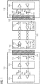
Fig. 1 illustrates a known concept of a USB interface including an AC coupling capacitor and a discharge resistor for AC coupling; -
Fig. 2 illustrates a USB interface having an ESD protection device for ESD protection and AC coupling; -
Fig. 3 illustrates a first example of the ESD protection device; -
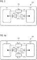
Fig. 4a illustrates a second example of the ESD protection device; -
Fig. 4b illustrates a layout of the second example of the ESD protection device; -
Fig. 5 illustrates a third example of the ESD protection device; -
Fig. 6 illustrates a layout of the third example of the ESD protection device; and -
Fig. 7 illustrates another layout of the third example of the ESD protection device. - Various examples will now be described more fully with reference to the accompanying drawings in which some examples are illustrated. In the figures, the thicknesses of lines, layers and/or regions may be exaggerated for clarity.
- Accordingly, while further examples are capable of various modifications and alternative forms, some particular examples thereof are shown in the figures and will subsequently be described in detail. However, this detailed description does not limit further examples to the particular forms described. Further examples may cover all modifications, equivalents, and alternatives falling within the scope of the disclosure. Same or like numbers refer to like or similar elements throughout the description of the figures, which may be implemented identically or in modified form when compared to one another while providing for the same or a similar functionality.
- It will be understood that when an element is referred to as being "connected" or "coupled" to another element, the elements may be directly connected or coupled via one or more intervening elements. If two elements A and B are combined using an "or", this is to be understood to disclose all possible combinations, i.e. only A, only B as well as A and B, if not explicitly or implicitly defined otherwise. An alternative wording for the same combinations is "at least one of A and B" or "A and/or B". The same applies, mutatis mutandis, for combinations of more than two Elements.
- The terminology used herein for the purpose of describing particular examples is not intended to be limiting for further examples. Whenever a singular form such as "a," "an" and "the" is used and using only a single element is neither explicitly or implicitly defined as being mandatory, further examples may also use plural elements to implement the same functionality. Likewise, when a functionality is subsequently described as being implemented using multiple elements, further examples may implement the same functionality using a single element or processing entity. It will be further understood that the terms "comprises," "comprising," "includes" and/or "including," when used, specify the presence of the stated features, integers, steps, operations, processes, acts, elements and/or components, but do not preclude the presence or addition of one or more other features, integers, steps, operations, processes, acts, elements, components and/or any group thereof.
- Unless otherwise defined, all terms (including technical and scientific terms) are used herein in their ordinary meaning of the art to which the examples belong.
-
Fig. 1 illustrates a known concept of a USB interface. In particular,Fig. 1 shows a circuit diagram schematically depicting a firstelectronic device 110 and a secondelectronic device 130 interconnected by theirUSB receptacles active cable 120 to enable a communication between the first and the secondelectronic device - The first
electronic device 110, for example, is a USB device, whereas the secondelectronic device 130 is a USB host. In an alternative configuration,device 110 may be a USB host anddevice 130 is a USB device. - As can be seen, the
USB device 110 and theUSB host 130 comprise adevice router 116 and ahost router 136, respectively, which can communicate with each other using a communication signal. TheUSB device 110 further includes are-timer 114 for a compensation of distortions of the communication signal. - The example of
Fig. 1 particularly relates to USB 3.2 orUSB 4 applications which may comprise an AC coupling functionality according to the "Universal Series Bus 4 (USB4) Specification (Version 1.0, August 2019). For AC coupling, theUSB device 110 and theUSB host 130 are equipped with a high passfilter including capacitors 142 andresistors 144 placed downstream from thereceptacles such capacitors 142 are disposed at ends of theactive cable 120. In this way, interfering DC components of the communication signal can be filtered out. - An implementation of a separate, discrete ESD protection device in the
USB device 110 and/or theUSB host 130 may lead to an increased part count, costs, and space requirements. Due to a limited installation space in some applications, the implementation of said discrete ESD protection device may not be possible. - With reference to
Fig. 2 , an improved concept for ESD protection in USB interfaces is shown. - Explicitly,
Fig. 2 shows anelectronic device 200 with aUSB interface 210 which can be a USB device, a USB hub or a USB host. Theelectronic device 200 can be a computer, a smartphone, a data (mass) storage, or another electronic device. TheUSB interface 210 particularly relates to USB 3.2 andUSB 4 applications. - The
USB interface 210 comprises aUSB router 216 and aUSB receptacle 212 for coupling theUSB router 216 to external devices. TheUSB receptacle 212, for example, is a USB Type-C receptacle. For differential signal transmission, an input (receive path) of theUSB router 216 includes a first and a second data line 248.1 and 248.2 connecting theUSB router 216 to theUSB receptacle 212. For AC coupling, anAC coupling capacitor 242 is placed in each of the data lines 248.1 and 248.2 between theUSB router 216 and theUSB receptacle 212. TheUSB router 216 and theAC coupling capacitors 242, for example, are arranged on a printed circuit board (PCB). - Each of the data lines 248.1 and 248.2 is coupled to an
ESD protection device 240 comprising adischarge resistor 244 and anESD protection component 246 which inFig. 2 includes a Zener diode. - A fundamental operating principle of the
ESD protection device 240 is that a conductivity of the ESD protection component 246 (e.g. the Zener diode) is (significantly) lower than that of theUSB router 216 or ideally zero if a voltage applied to the USB interface 210 (i.e. the USB receptacle 212) falls short of a predefined (hazardous) voltage level, and increases if an over-voltage exceeding the predefined voltage level is applied. - This enables the
ESD protection device 240 to drain the over-voltage exceeding the said predefined voltage level to an external (e.g. ground)potential 249, e.g. in the event of an ESD strike, and protect theUSB router 216 from hazardous over-voltages. In particular, the conductivity of theESD protection component 246 can exceed the conductivity of theUSB router 216. - To this end, a breakdown voltage of the
ESD protection component 246 can be set such that over-voltages (e.g. resulting from ESD strikes) hazardous to theUSB router 216 lead to a breakdown of theESD protection component 246 and the over-voltages can be drained via theESD protection component 246. In this way, theESD protection component 246 limits the voltage applied to theUSB interface 210. A skilled person having benefit from the present disclosure will appreciate that the breakdown voltage of theESD protection component 246 can be adjusted by its internal structure (e.g. its doping) to adapt theESD protection device 240 to different applications. - During "regular" operation, when the voltage applied by a communication signal is lower than the predefined voltage level, a resistance of the
ESD protection component 246 in the direction of theexternal potential 249 is higher than that of thedischarge resistor 244 and theAC coupling capacitor 242 is predominately discharged by thedischarge resistor 244. The higher the resistance of theESD protection component 246 during regular operation is, the lower may be an undesired leakage current via theESD protection device 240. - The skilled person will appreciate that the
ESD protection device 240 can additionally or alternatively be used to protect theUSB interface 210 from over-voltages which do not result from ESD strikes but from operating errors or malfunctions. - Alternatively, the ESD protection component can comprise one or more varistors, thyristors, other diodes (e.g. avalanche diodes, transient-voltage-suppression diodes), or combinations thereof. Combinations of multiple diodes, for example, are used for "bidirectional" ESD protection, as stated in more detail later.
- The
ESD protection component 246 and thedischarge resistor 244 are incorporated in a singleelectronic component 245 which can be placed on the PCB carrying theUSB router 216 and theAC coupling capacitors 242. This allows a more space-saving integration of thedischarge resistor 244 and theESD protection component 246 than a separate arrangement of, for example, a discrete discharge resistor and a discrete ESD protection component. - The
electronic component 245 can be configured as a packaged component or a bare die assembly, both of which can comprise one or multiple dies or substrates. Thus, thedischarge resistor 244 and theESD protection component 246 can be arranged on a mutual die/substrate or separate dies/substrates of the packaged component or the bare die assembly, respectively. - In the following examples,
discharge resistor 244 and ESD protection component are arranged on a mutual (i.e. same) die. - Examples of a packaged component are a chip-scale package (CSP), small outline package (SOP), flat package, and a surface-mounted device (SMD).
- The
ESD protection component 246 and thedischarge resistor 244 can be coupled to the data lines 248.1 and 248.2, respectively, via a single pad of theelectronic component 245. Hence, a number of solder joints and electrical parasitics thereof may be reduced compared to the separate arrangement of the discrete resistor and ESD protection component. - In addition, production costs can be reduced by the integration of the
ESD protection component 246 and thedischarge resistor 244 in the singleelectronic component 245. - The above
electronic component 245 can further enable an integration of ESD protection or AC coupling in applications where no dedicated place was reserved for it, for example, by replacing a discrete discharge resistor with theelectronic component 245. - It is noted that even though
Fig. 2 merely addresses the (data) input (receive path) of theUSB router 216, theESD protection device 240 herein can be additionally or alternatively applied to an (data) output (transmit path) of theUSB router 216. - In the receive path of
USB 4 applications, theAC coupling capacitors 242 may have a capacitance between 300 nF and 363 nF and thedischarge resistors 244 may have a resistance between 200 kΩ and 242 Ω. - In the transmit path of
USB 4 applications, theAC coupling capacitors 242 may have a capacitance between 135 nF and 265 nF. -
Fig. 3 shows an example of theelectronic component 245 where theESD protection component 246 connecting afirst pad 241 and asecond pad 243 of theESD protection device 240 comprises a first diode 246.1 and a second diode 246.2 connected "back-to-back" to each other. That is, forward directions, as well as reverse directions of the first and the second 246.1 and 246.2, are opposite to each other. Thus, theESD protection component 246 enables (bidirectional) ESD protection from positive and negative over-voltages. To be more specific, the first and the second diode 246.1 and 246.2 are connected serially to each other. In some embodiments, the first and the second diode 246.1 and 246.2 may alternatively be connected in parallel to each other. - The first and the second diode 246.1 and 246.2 again can be Zener diodes, avalanche diodes, Schottky diodes or a combination thereof.
- Due to the bidirectional ESD protection, either the
first pad 241 can be connected to the external (ground)potential 249, while thesecond pad 243 can be connected to theUSB interface 210 or vice versa. - In
Fig. 3 , thedischarge resistor 244 with resistance Rbs is connected in parallel to the first and the second diode 246.1 and 246.2. - It is noted that
Fig. 3 merely illustrates a schematic circuit diagram of theelectronic component 245. In practice, the first, and the second diode 246.1 and 246.2 can be placed differently than shown inFig. 3 . -
Fig. 4a illustrates another example of theelectronic component 245 where thedischarge resistor 244 is replaced by a first resistor 244.1 and a second resistor 244.2 connected in parallel, each of the resistors 244.1 and 244.2 having half the resistance Rbs of thedischarge resistor 244. - Separate resistors (i.e. the first and the second resistor 244.1 and 244.2) may be technically easier to produce and/or implement than a single one (e.g. discharge resistor 244).
-
Fig. 4b shows an optional layout of the previous example of theESD protection device 240. - As can be seen in
Fig. 4b , the first and the second resistor 244.1 and 244.2, for example, are preferably configured as a meander line (e.g. polysilicon) resistors, as they are (technically) easier to design and manufacture vis-à-vis other resistors. -
Fig. 5 shows another example of theESD protection device 240. InFig. 5 , theESD protection component 246 comprises a first semiconductor device 247.1 and a second semiconductor device 247.2 both having four layers of alternating p- and n-type materials (here indicated by the circuit symbol of a thyristor).The first and the second semiconductor device 247.1 and 247.2 are connected in parallel to each other, i.e. in a so-called "parallel configuration". Moreover, the first and the second semiconductor device 247.1 and 247.2 are arranged "back-to-back". That is, the first and the second semiconductor device 247.1 and 247.2 have opposite forward directions and opposite reverse directions to enable bidirectional over-voltage or ESD protection. Moreover, the first and the semiconductor device 247.1 and 247.1 protect each other from damages resulting from over-voltages in reverse direction in the aforementioned back-to-back arrangement. - The skilled person having benefit from the present disclosure will appreciate that thyristors (e.g. the first and the second thyristor 247.1 and 247.2) may provide an improved protection performance vis-á-vis diodes in ESD protection components due to their "deeper snapback" and lower clamping voltage.
- The (single)
discharge resistor 244 is connected in parallel to the first and the second thyristor 247.1 and 247.2. -
Fig. 6 shows another example of theESD protection device 240. - In
Fig. 6 , theESD protection device 240 includes a first serial resistor 244a and a secondserial resistor 244b connected in series to each other, while first and the second diode 246.1 and 246.2. are connected in parallel to theserial resistors 244a and 244b. The first and the secondserial resistor 244a and 244b, for example, are configured as a polysilicon resistor formed in a polysilicon layer beneath the first and thesecond pad - Similarly, the first and the second diode 246.1 and 246.2 can be formed in the polysilicon layer.
- Analogously, the
discharge resistor 244 inFig. 7 may be a polysilicon resistor formed in the polysilicon layer adjacent to thefirst pad 241. Thedischarge resistor 244 is coupled to a connection of the first diode 246.1 to thesecond pad 243. - It should be noted, that the above examples merely partly cover an entirety of various possible embodiments and that the features (e.g. diodes and resistors) described in
Fig. 2 to 7 can be combined in different ways to realize the aforementioned concept. - The examples as described herein may be summarized as follows:
Examples of the present disclosure relate to an ESD protection device for a USB interface. The ESD protection device comprises an ESD protection component configured to limit a voltage applied to the USB interface and at least one discharge resistor configured to discharge an AC coupling capacitor of the USB interface The ESD protection component and the discharge resistor are incorporated in a single electronic component. - In some examples, the electronic component is configured as at least one of a packaged electronic component and a bare die assembly.
- According to some examples, the electronic component is configured as a packaged electronic component.
- In some examples, the electronic component is configured as a bare die assembly.
- According to some examples, the ESD protection component and the discharge resistor are disposed on a single die of the electronic component.
- In some examples, the electronic component comprises a first die and a second die, wherein the ESD protection component is disposed on the first die and the discharge resistor is disposed on the second die.
- According to some examples, the AC coupling capacitor has a capacitance between 300 nF and 363 nF and the discharge resistor has a resistance between 200 kΩ and 242 kΩ.
- In some examples, the AC coupling capacitor has a capacitance between 100 nF and 500 nF.
- According to some examples, the ESD protection component comprises at least one diode configured to limit the voltage applied to the USB interface.
- In some examples, the ESD protection component comprises a pair of back-to-back diodes configured to limit the voltage applied to the USB interface.
- According to some examples, the ESD protection component comprises a semiconductor device having four layers of alternating p- and n-type materials, wherein the semiconductor device is configured to limit the voltage applied to the USB interface.
- Some examples relate to an electronic device comprising a USB interface which comprises at least one AC coupling capacitor and at least one ESD protection device comprising. The ESD protection device comprises an ESD protection component configured to limit a voltage applied to the USB interface and at least one discharge resistor configured to discharge the AC coupling capacitor of the USB interface. The ESD protection component and the discharge resistor are incorporated in a single electronic component.
- In some examples, the electronic component is configured as at least one of a packaged electronic component and a bare die assembly.
- According to some examples, the electronic device comprises a first ESD protection device comprising a first ESD protection component configured to limit the voltage applied to the USB interface and a first discharge resistor configured to discharge a first AC coupling capacitor of the USB interface. The first ESD protection component and the first discharge resistor are incorporated in a single first electronic component. The electronic device further comprises a second ESD protection device comprising a second ESD protection component configured to limit the voltage applied to the USB interface and a second discharge resistor configured to discharge a second AC coupling capacitor of the USB interface. The second ESD protection component and the second discharge resistor are incorporated in a single second electronic component.
- The aspects and features mentioned and described together with one or more of the previously detailed examples and figures, may as well be combined with one or more of the other examples in order to replace a like feature of the other example or in order to additionally introduce the feature to the other example.
- The description and drawings merely illustrate the principles of the disclosure. Furthermore, all examples recited herein are principally intended expressly to be only for illustrative purposes to aid the reader in understanding the principles of the disclosure and the concepts contributed by the inventor(s) to furthering the art. All statements herein reciting principles, aspects, and examples of the disclosure, as well as specific examples thereof, are intended to encompass equivalents thereof.
- A functional block denoted as "means for ..." performing a certain function may refer to a circuit that is configured to perform a certain function. Hence, a "means for s.th." may be implemented as a "means configured to or suited for s.th.", such as a device or a circuit configured to or suited for the respective task.
- It is to be understood that the disclosure of multiple acts, processes, operations, steps or functions disclosed in the specification or claims may not be construed as to be within the specific order, unless explicitly or implicitly stated otherwise, for instance for technical reasons. Therefore, the disclosure of multiple acts or functions will not limit these to a particular order unless such acts or functions are not interchangeable for technical reasons. Furthermore, in some examples a single act, function, process, operation or step may include or may be broken into multiple sub-acts, -functions, -processes, -operations or -steps, respectively. Such sub acts may be included and part of the disclosure of this single act unless explicitly excluded.
- Furthermore, the following claims are hereby incorporated into the detailed description, where each claim may stand on its own as a separate example. While each claim may stand on its own as a separate example, it is to be noted that - although a dependent claim may refer in the claims to a specific combination with one or more other claims - other examples may also include a combination of the dependent claim with the subject matter of each other dependent or independent claim. Such combinations are explicitly proposed herein unless it is stated that a specific combination is not intended. Furthermore, it is intended to include also features of a claim to any other independent claim even if this claim is not directly made dependent to the independent claim.
Claims (14)
- An electrostatic discharge, ESD, protection device (240) for a Universal Serial Bus, USB, interface (210), the ESD protection device (240) comprising:an ESD protection component (246) configured to limit a voltage applied to the USB interface (210); andat least one discharge resistor (244, 244.1, 244.2) configured to discharge an AC coupling capacitor (242) of the USB interface (210),wherein the ESD protection component (246) and the discharge resistor (244, 244.1, 244.2) are incorporated in a single electronic component (245).
- The ESD protection device (240) of claim 1, wherein the electronic component (245) is configured as at least one of a packaged electronic component and a bare die assembly.
- The ESD protection device (240) of claim 2, wherein the electronic component (245) is configured as a packaged electronic component.
- The ESD protection device (240) of claim 2, wherein the electronic component (245) is configured as a bare die assembly.
- The ESD protection device (240) of any one of the preceding claims, wherein the ESD protection component (246) and the discharge resistor (244, 244.1, 244.2) are disposed on a single die of the electronic component (245).
- The ESD protection device (240) of any one of the preceding claims, wherein the electronic component (245) comprises a first die and a second die, wherein the ESD protection component (246) is disposed on the first die and the discharge resistor (244, 244.1, 244.2) is disposed on the second die.
- The ESD protection device (240) of any one of the preceding claims,
wherein the AC coupling capacitor (242) has a capacitance between 300 nF and 363 nF; and
wherein the discharge resistor (244, 244.1 244.2) has a resistance between 200 kΩ and 242 kΩ. - The ESD protection device (240) of any one of the claims 1 to 7, wherein the AC coupling capacitor (242) has a capacitance between 100 nF and 500 nF.
- The ESD protection device (240) of any one of the preceding claims, wherein the ESD protection component (246) comprises at least one diode (246, 246.1, 246.2) configured to limit the voltage applied to the USB interface (210).
- The ESD protection device of claim 10, wherein the ESD protection component (246) comprises a pair of diodes (246.1, 246.2) configured to limit the voltage applied to the USB interface (210), wherein the pair of diodes (246.1, 246.2) is coupled back-to-back.
- The ESD protection device (240) of any one of the preceding claims, wherein the ESD protection component (246) comprises a semiconductor device (247.1, 247.2) having four layers of alternating p- and n-type materials, and wherein the semiconductor device (247.1 and 247.2) is configured to limit the voltage applied to the USB interface (210).
- An electronic device (200) comprising:a Universal Serial Bus, USB, interface (210) comprising at least one AC coupling capacitor (242); andat least one electrostatic discharge, ESD, protection device (240) comprising:an ESD protection component (246) configured to limit a voltage applied to the USB interface (210); andat least one discharge resistor (244, 244.1, 244.2) configured to discharge the AC coupling capacitor (242),wherein the ESD protection component (246) and the discharge resistor (244, 244.1, 244.2) are incorporated in a single electronic component (245).
- The electronic device (200) of claim 12, wherein the electronic component is configured as at least one of a packaged electronic component and a bare die assembly.
- The electronic device (200) of claim 12 or 13, comprising:a first ESD protection device (240) comprising:a first ESD protection component (246) configured to limit the voltage applied to the USB interface (210); anda first discharge resistor (244, 244.1, 244.2) configured to discharge a first AC coupling capacitor (242) of the USB interface (210),wherein the first ESD protection component (246) and the first discharge resistor (244, 244.1, 244.2) are incorporated in a single first electronic component (245); anda second ESD protection device comprising:a second ESD protection component (246) configured to limit the voltage applied to the USB interface (210); anda second discharge resistor (244, 244.1, 244.2) configured to discharge a second AC coupling capacitor (242) of the USB interface (210),wherein the second ESD protection component (246) and the second discharge resistor (244, 244.1, 244.2) are incorporated in a single second electronic component (245).
Priority Applications (3)
| Application Number | Priority Date | Filing Date | Title |
|---|---|---|---|
| EP20183688.9A EP3933603B1 (en) | 2020-07-02 | 2020-07-02 | An electrostatic discharge, esd, protection device for a universal serial bus, usb, interface |
| US17/341,982 US11670940B2 (en) | 2020-07-02 | 2021-06-08 | Electrostatic discharge, ESD, protection device for a Universal Serial Bus, USB, interface |
| CN202110742829.9A CN113889993A (en) | 2020-07-02 | 2021-07-01 | Electrostatic discharge ESD protection device for universal serial bus USB interface |
Applications Claiming Priority (1)
| Application Number | Priority Date | Filing Date | Title |
|---|---|---|---|
| EP20183688.9A EP3933603B1 (en) | 2020-07-02 | 2020-07-02 | An electrostatic discharge, esd, protection device for a universal serial bus, usb, interface |
Publications (2)
| Publication Number | Publication Date |
|---|---|
| EP3933603A1 true EP3933603A1 (en) | 2022-01-05 |
| EP3933603B1 EP3933603B1 (en) | 2024-08-28 |
Family
ID=71452143
Family Applications (1)
| Application Number | Title | Priority Date | Filing Date |
|---|---|---|---|
| EP20183688.9A Active EP3933603B1 (en) | 2020-07-02 | 2020-07-02 | An electrostatic discharge, esd, protection device for a universal serial bus, usb, interface |
Country Status (3)
| Country | Link |
|---|---|
| US (1) | US11670940B2 (en) |
| EP (1) | EP3933603B1 (en) |
| CN (1) | CN113889993A (en) |
Families Citing this family (1)
| Publication number | Priority date | Publication date | Assignee | Title |
|---|---|---|---|---|
| FR3122769A1 (en) * | 2021-05-07 | 2022-11-11 | Stmicroelectronics (Tours) Sas | One-way transient voltage suppression device without live conduction |
Citations (5)
| Publication number | Priority date | Publication date | Assignee | Title |
|---|---|---|---|---|
| US20100084551A1 (en) * | 2006-11-02 | 2010-04-08 | Shimadzu Corporation | Input protection circuit for high-speed analogue signal and time-of-flight mass spectrometer |
| EP2498167A1 (en) * | 2006-12-08 | 2012-09-12 | Nokia Corporation | Multiple connections to a single serial interface |
| EP2849023A1 (en) * | 2012-05-11 | 2015-03-18 | Fujitsu Limited | Electronic device and control method therefor |
| CN104979874A (en) * | 2015-07-10 | 2015-10-14 | 成都市宏山科技有限公司 | Usb interface charging circuit |
| US20200036563A1 (en) * | 2018-07-26 | 2020-01-30 | Advanced Micro Devices, Inc. | Passive continuous-time linear equalizer |
Family Cites Families (18)
| Publication number | Priority date | Publication date | Assignee | Title |
|---|---|---|---|---|
| US7649726B2 (en) * | 2004-08-16 | 2010-01-19 | National Instruments Corporation | Protection circuit for general-purpose digital I/O lines |
| US7355476B2 (en) * | 2005-06-30 | 2008-04-08 | Silicon Laboratories Inc. | Input stage for an amplifier |
| US8346198B2 (en) * | 2005-06-30 | 2013-01-01 | Silicon Laboratories Inc. | Low noise amplifier for a radio receiver |
| US7855866B2 (en) * | 2006-12-19 | 2010-12-21 | Akros Silicon, Inc. | Network interface with transient protection apparatus for multiple ground planes |
| CN101281417B (en) * | 2007-04-06 | 2011-11-09 | 鸿富锦精密工业(深圳)有限公司 | Power supply switching device |
| US8537517B1 (en) * | 2011-04-26 | 2013-09-17 | Manufacturing Networks Incorporated | System and method for fast-acting power protection |
| US9093977B2 (en) * | 2012-07-31 | 2015-07-28 | Taiwan Semiconductor Manufacturing Co., Ltd. | Integrated passive device filter with fully on-chip ESD protection |
| KR101495736B1 (en) * | 2013-05-15 | 2015-02-25 | 전북대학교산학협력단 | ESD-EMI common mode filter device and the fabrication method |
| CN203607833U (en) * | 2013-10-25 | 2014-05-21 | 海能达通信股份有限公司 | An explosion-proof electric device |
| US10164423B2 (en) * | 2014-08-19 | 2018-12-25 | Microchip Technology Incorporated | Method and system for ground plane isolation |
| US10082853B2 (en) * | 2015-02-23 | 2018-09-25 | Ortronics, Inc. | USB power delivery extension system |
| JP6641388B2 (en) * | 2015-05-14 | 2020-02-05 | 日本テキサス・インスツルメンツ合同会社 | USB controller ESD protection device and method |
| US10855069B2 (en) * | 2018-04-17 | 2020-12-01 | Texas Instruments Incorporated | USB type-C/PD controller having integrated VBUS to CC short protection |
| US10826291B2 (en) * | 2018-09-12 | 2020-11-03 | CoolStar Technology, Inc. | Electrostatic discharge transient power clamp |
| US10483757B1 (en) * | 2018-09-18 | 2019-11-19 | Manufacturing Networks Incorporated (MNI) | Fast-acting power protection system incorporating discrete MOSFETs and control IC on hybrid substrates and method of operating thereof |
| US10312742B1 (en) * | 2018-10-08 | 2019-06-04 | Jenan E. S. SH. M. Al-Shehab | Wireless power transmission system |
| US10742227B1 (en) * | 2019-02-25 | 2020-08-11 | Intel Corporation | Differential source follower with current steering devices |
| US20210098987A1 (en) * | 2019-09-26 | 2021-04-01 | Priya Walimbe | Electrostatic discharge protection for stacked-die system |
-
2020
- 2020-07-02 EP EP20183688.9A patent/EP3933603B1/en active Active
-
2021
- 2021-06-08 US US17/341,982 patent/US11670940B2/en active Active
- 2021-07-01 CN CN202110742829.9A patent/CN113889993A/en active Pending
Patent Citations (5)
| Publication number | Priority date | Publication date | Assignee | Title |
|---|---|---|---|---|
| US20100084551A1 (en) * | 2006-11-02 | 2010-04-08 | Shimadzu Corporation | Input protection circuit for high-speed analogue signal and time-of-flight mass spectrometer |
| EP2498167A1 (en) * | 2006-12-08 | 2012-09-12 | Nokia Corporation | Multiple connections to a single serial interface |
| EP2849023A1 (en) * | 2012-05-11 | 2015-03-18 | Fujitsu Limited | Electronic device and control method therefor |
| CN104979874A (en) * | 2015-07-10 | 2015-10-14 | 成都市宏山科技有限公司 | Usb interface charging circuit |
| US20200036563A1 (en) * | 2018-07-26 | 2020-01-30 | Advanced Micro Devices, Inc. | Passive continuous-time linear equalizer |
Also Published As
| Publication number | Publication date |
|---|---|
| US20220006289A1 (en) | 2022-01-06 |
| CN113889993A (en) | 2022-01-04 |
| EP3933603B1 (en) | 2024-08-28 |
| US11670940B2 (en) | 2023-06-06 |
Similar Documents
| Publication | Publication Date | Title |
|---|---|---|
| US8552530B2 (en) | Vertical transient voltage suppressors | |
| US20150255930A1 (en) | Interfaces with built-in transient voltage suppression | |
| KR20150135909A (en) | Composite electronic component, manufacturing method thereof, board for mounting the same and packing unit thereof | |
| CN104135148A (en) | USB (Universal Serial Bus) interface circuit | |
| CN1897785A (en) | System and method for electrostatic discharge protection in an electronic circuit | |
| US9819176B2 (en) | Low capacitance transient voltage suppressor | |
| EP3648163B1 (en) | Discharge protection circuit and method for operating a discharge protection circuit | |
| US12388253B2 (en) | Electrostatic discharge protection device with integrated series resistors | |
| US11670940B2 (en) | Electrostatic discharge, ESD, protection device for a Universal Serial Bus, USB, interface | |
| JP2008028214A (en) | Static electricity countermeasure circuit | |
| KR20170141631A (en) | Composite electronic component, manufacturing method thereof, board for mounting the same and packing unit thereof | |
| US7675723B2 (en) | Transient to digital converters | |
| EP1981255B1 (en) | Surge protection circuit for ORing circuitry of power supplies | |
| EP3471230B1 (en) | Interface protection circuit and device interface | |
| US12244137B2 (en) | ESD protection for multi-die integrated circuits (ICs) including integrated passive devices | |
| US10320968B2 (en) | Protection module and decoupling component thereof for symmetrical twisted pairs | |
| CN104282666A (en) | Electrical signal transmission device and integrated circuit | |
| CN110138189B (en) | Protection circuit for Ethernet and power supply end equipment with protection circuit | |
| EP2335283B1 (en) | Protection for an integrated circuit | |
| CN207150165U (en) | CAN circuit interface electrostatic discharge module | |
| CN206962436U (en) | Protection circuit, equipment and communication system | |
| TWI499143B (en) | Surge protection circuit applied in connector | |
| US20250167543A1 (en) | Integrated circuit capable of withstanding electrical over stress | |
| CN215221019U (en) | Circuit and electronic equipment capable of realizing electrostatic protection of antenna end | |
| KR20180134127A (en) | Electrical overstress protection device |
Legal Events
| Date | Code | Title | Description |
|---|---|---|---|
| PUAI | Public reference made under article 153(3) epc to a published international application that has entered the european phase |
Free format text: ORIGINAL CODE: 0009012 |
|
| STAA | Information on the status of an ep patent application or granted ep patent |
Free format text: STATUS: EXAMINATION IS IN PROGRESS |
|
| 17P | Request for examination filed |
Effective date: 20210316 |
|
| AK | Designated contracting states |
Kind code of ref document: A1 Designated state(s): AL AT BE BG CH CY CZ DE DK EE ES FI FR GB GR HR HU IE IS IT LI LT LU LV MC MK MT NL NO PL PT RO RS SE SI SK SM TR |
|
| B565 | Issuance of search results under rule 164(2) epc |
Effective date: 20201222 |
|
| GRAP | Despatch of communication of intention to grant a patent |
Free format text: ORIGINAL CODE: EPIDOSNIGR1 |
|
| STAA | Information on the status of an ep patent application or granted ep patent |
Free format text: STATUS: GRANT OF PATENT IS INTENDED |
|
| INTG | Intention to grant announced |
Effective date: 20240215 |
|
| GRAS | Grant fee paid |
Free format text: ORIGINAL CODE: EPIDOSNIGR3 |
|
| P01 | Opt-out of the competence of the unified patent court (upc) registered |
Effective date: 20240507 |
|
| GRAA | (expected) grant |
Free format text: ORIGINAL CODE: 0009210 |
|
| STAA | Information on the status of an ep patent application or granted ep patent |
Free format text: STATUS: THE PATENT HAS BEEN GRANTED |
|
| AK | Designated contracting states |
Kind code of ref document: B1 Designated state(s): AL AT BE BG CH CY CZ DE DK EE ES FI FR GB GR HR HU IE IS IT LI LT LU LV MC MK MT NL NO PL PT RO RS SE SI SK SM TR |
|
| REG | Reference to a national code |
Ref country code: CH Ref legal event code: EP |
|
| REG | Reference to a national code |
Ref country code: DE Ref legal event code: R096 Ref document number: 602020036531 Country of ref document: DE |
|
| REG | Reference to a national code |
Ref country code: IE Ref legal event code: FG4D |
|
| REG | Reference to a national code |
Ref country code: LT Ref legal event code: MG9D |
|
| PG25 | Lapsed in a contracting state [announced via postgrant information from national office to epo] |
Ref country code: NO Free format text: LAPSE BECAUSE OF FAILURE TO SUBMIT A TRANSLATION OF THE DESCRIPTION OR TO PAY THE FEE WITHIN THE PRESCRIBED TIME-LIMIT Effective date: 20241128 |
|
| REG | Reference to a national code |
Ref country code: AT Ref legal event code: MK05 Ref document number: 1718724 Country of ref document: AT Kind code of ref document: T Effective date: 20240828 |
|
| PG25 | Lapsed in a contracting state [announced via postgrant information from national office to epo] |
Ref country code: NL Free format text: LAPSE BECAUSE OF FAILURE TO SUBMIT A TRANSLATION OF THE DESCRIPTION OR TO PAY THE FEE WITHIN THE PRESCRIBED TIME-LIMIT Effective date: 20240828 Ref country code: PT Free format text: LAPSE BECAUSE OF FAILURE TO SUBMIT A TRANSLATION OF THE DESCRIPTION OR TO PAY THE FEE WITHIN THE PRESCRIBED TIME-LIMIT Effective date: 20241230 Ref country code: FI Free format text: LAPSE BECAUSE OF FAILURE TO SUBMIT A TRANSLATION OF THE DESCRIPTION OR TO PAY THE FEE WITHIN THE PRESCRIBED TIME-LIMIT Effective date: 20240828 Ref country code: GR Free format text: LAPSE BECAUSE OF FAILURE TO SUBMIT A TRANSLATION OF THE DESCRIPTION OR TO PAY THE FEE WITHIN THE PRESCRIBED TIME-LIMIT Effective date: 20241129 Ref country code: PL Free format text: LAPSE BECAUSE OF FAILURE TO SUBMIT A TRANSLATION OF THE DESCRIPTION OR TO PAY THE FEE WITHIN THE PRESCRIBED TIME-LIMIT Effective date: 20240828 |
|
| PG25 | Lapsed in a contracting state [announced via postgrant information from national office to epo] |
Ref country code: BG Free format text: LAPSE BECAUSE OF FAILURE TO SUBMIT A TRANSLATION OF THE DESCRIPTION OR TO PAY THE FEE WITHIN THE PRESCRIBED TIME-LIMIT Effective date: 20240828 |
|
| PG25 | Lapsed in a contracting state [announced via postgrant information from national office to epo] |
Ref country code: LV Free format text: LAPSE BECAUSE OF FAILURE TO SUBMIT A TRANSLATION OF THE DESCRIPTION OR TO PAY THE FEE WITHIN THE PRESCRIBED TIME-LIMIT Effective date: 20240828 |
|
| REG | Reference to a national code |
Ref country code: NL Ref legal event code: MP Effective date: 20240828 |
|
| PG25 | Lapsed in a contracting state [announced via postgrant information from national office to epo] |
Ref country code: IS Free format text: LAPSE BECAUSE OF FAILURE TO SUBMIT A TRANSLATION OF THE DESCRIPTION OR TO PAY THE FEE WITHIN THE PRESCRIBED TIME-LIMIT Effective date: 20241228 Ref country code: AT Free format text: LAPSE BECAUSE OF FAILURE TO SUBMIT A TRANSLATION OF THE DESCRIPTION OR TO PAY THE FEE WITHIN THE PRESCRIBED TIME-LIMIT Effective date: 20240828 |
|
| PG25 | Lapsed in a contracting state [announced via postgrant information from national office to epo] |
Ref country code: HR Free format text: LAPSE BECAUSE OF FAILURE TO SUBMIT A TRANSLATION OF THE DESCRIPTION OR TO PAY THE FEE WITHIN THE PRESCRIBED TIME-LIMIT Effective date: 20240828 |
|
| PG25 | Lapsed in a contracting state [announced via postgrant information from national office to epo] |
Ref country code: RS Free format text: LAPSE BECAUSE OF FAILURE TO SUBMIT A TRANSLATION OF THE DESCRIPTION OR TO PAY THE FEE WITHIN THE PRESCRIBED TIME-LIMIT Effective date: 20241128 Ref country code: ES Free format text: LAPSE BECAUSE OF FAILURE TO SUBMIT A TRANSLATION OF THE DESCRIPTION OR TO PAY THE FEE WITHIN THE PRESCRIBED TIME-LIMIT Effective date: 20240828 |
|
| PG25 | Lapsed in a contracting state [announced via postgrant information from national office to epo] |
Ref country code: RS Free format text: LAPSE BECAUSE OF FAILURE TO SUBMIT A TRANSLATION OF THE DESCRIPTION OR TO PAY THE FEE WITHIN THE PRESCRIBED TIME-LIMIT Effective date: 20241128 Ref country code: PT Free format text: LAPSE BECAUSE OF FAILURE TO SUBMIT A TRANSLATION OF THE DESCRIPTION OR TO PAY THE FEE WITHIN THE PRESCRIBED TIME-LIMIT Effective date: 20241230 Ref country code: PL Free format text: LAPSE BECAUSE OF FAILURE TO SUBMIT A TRANSLATION OF THE DESCRIPTION OR TO PAY THE FEE WITHIN THE PRESCRIBED TIME-LIMIT Effective date: 20240828 Ref country code: NO Free format text: LAPSE BECAUSE OF FAILURE TO SUBMIT A TRANSLATION OF THE DESCRIPTION OR TO PAY THE FEE WITHIN THE PRESCRIBED TIME-LIMIT Effective date: 20241128 Ref country code: NL Free format text: LAPSE BECAUSE OF FAILURE TO SUBMIT A TRANSLATION OF THE DESCRIPTION OR TO PAY THE FEE WITHIN THE PRESCRIBED TIME-LIMIT Effective date: 20240828 Ref country code: LV Free format text: LAPSE BECAUSE OF FAILURE TO SUBMIT A TRANSLATION OF THE DESCRIPTION OR TO PAY THE FEE WITHIN THE PRESCRIBED TIME-LIMIT Effective date: 20240828 Ref country code: IS Free format text: LAPSE BECAUSE OF FAILURE TO SUBMIT A TRANSLATION OF THE DESCRIPTION OR TO PAY THE FEE WITHIN THE PRESCRIBED TIME-LIMIT Effective date: 20241228 Ref country code: HR Free format text: LAPSE BECAUSE OF FAILURE TO SUBMIT A TRANSLATION OF THE DESCRIPTION OR TO PAY THE FEE WITHIN THE PRESCRIBED TIME-LIMIT Effective date: 20240828 Ref country code: GR Free format text: LAPSE BECAUSE OF FAILURE TO SUBMIT A TRANSLATION OF THE DESCRIPTION OR TO PAY THE FEE WITHIN THE PRESCRIBED TIME-LIMIT Effective date: 20241129 Ref country code: FI Free format text: LAPSE BECAUSE OF FAILURE TO SUBMIT A TRANSLATION OF THE DESCRIPTION OR TO PAY THE FEE WITHIN THE PRESCRIBED TIME-LIMIT Effective date: 20240828 Ref country code: ES Free format text: LAPSE BECAUSE OF FAILURE TO SUBMIT A TRANSLATION OF THE DESCRIPTION OR TO PAY THE FEE WITHIN THE PRESCRIBED TIME-LIMIT Effective date: 20240828 Ref country code: BG Free format text: LAPSE BECAUSE OF FAILURE TO SUBMIT A TRANSLATION OF THE DESCRIPTION OR TO PAY THE FEE WITHIN THE PRESCRIBED TIME-LIMIT Effective date: 20240828 Ref country code: AT Free format text: LAPSE BECAUSE OF FAILURE TO SUBMIT A TRANSLATION OF THE DESCRIPTION OR TO PAY THE FEE WITHIN THE PRESCRIBED TIME-LIMIT Effective date: 20240828 |
|
| PG25 | Lapsed in a contracting state [announced via postgrant information from national office to epo] |
Ref country code: RO Free format text: LAPSE BECAUSE OF FAILURE TO SUBMIT A TRANSLATION OF THE DESCRIPTION OR TO PAY THE FEE WITHIN THE PRESCRIBED TIME-LIMIT Effective date: 20240828 Ref country code: DK Free format text: LAPSE BECAUSE OF FAILURE TO SUBMIT A TRANSLATION OF THE DESCRIPTION OR TO PAY THE FEE WITHIN THE PRESCRIBED TIME-LIMIT Effective date: 20240828 Ref country code: SM Free format text: LAPSE BECAUSE OF FAILURE TO SUBMIT A TRANSLATION OF THE DESCRIPTION OR TO PAY THE FEE WITHIN THE PRESCRIBED TIME-LIMIT Effective date: 20240828 |
|
| PG25 | Lapsed in a contracting state [announced via postgrant information from national office to epo] |
Ref country code: EE Free format text: LAPSE BECAUSE OF FAILURE TO SUBMIT A TRANSLATION OF THE DESCRIPTION OR TO PAY THE FEE WITHIN THE PRESCRIBED TIME-LIMIT Effective date: 20240828 |
|
| PG25 | Lapsed in a contracting state [announced via postgrant information from national office to epo] |
Ref country code: CZ Free format text: LAPSE BECAUSE OF FAILURE TO SUBMIT A TRANSLATION OF THE DESCRIPTION OR TO PAY THE FEE WITHIN THE PRESCRIBED TIME-LIMIT Effective date: 20240828 |
|
| PG25 | Lapsed in a contracting state [announced via postgrant information from national office to epo] |
Ref country code: SK Free format text: LAPSE BECAUSE OF FAILURE TO SUBMIT A TRANSLATION OF THE DESCRIPTION OR TO PAY THE FEE WITHIN THE PRESCRIBED TIME-LIMIT Effective date: 20240828 Ref country code: IT Free format text: LAPSE BECAUSE OF FAILURE TO SUBMIT A TRANSLATION OF THE DESCRIPTION OR TO PAY THE FEE WITHIN THE PRESCRIBED TIME-LIMIT Effective date: 20240828 |
|
| REG | Reference to a national code |
Ref country code: DE Ref legal event code: R097 Ref document number: 602020036531 Country of ref document: DE |
|
| PLBE | No opposition filed within time limit |
Free format text: ORIGINAL CODE: 0009261 |
|
| STAA | Information on the status of an ep patent application or granted ep patent |
Free format text: STATUS: NO OPPOSITION FILED WITHIN TIME LIMIT |
|
| 26N | No opposition filed |
Effective date: 20250530 |
|
| PG25 | Lapsed in a contracting state [announced via postgrant information from national office to epo] |
Ref country code: SE Free format text: LAPSE BECAUSE OF FAILURE TO SUBMIT A TRANSLATION OF THE DESCRIPTION OR TO PAY THE FEE WITHIN THE PRESCRIBED TIME-LIMIT Effective date: 20240828 |
|
| PGFP | Annual fee paid to national office [announced via postgrant information from national office to epo] |
Ref country code: DE Payment date: 20250915 Year of fee payment: 6 |
|
| REG | Reference to a national code |
Ref country code: CH Ref legal event code: H13 Free format text: ST27 STATUS EVENT CODE: U-0-0-H10-H13 (AS PROVIDED BY THE NATIONAL OFFICE) Effective date: 20260224 |
|
| PG25 | Lapsed in a contracting state [announced via postgrant information from national office to epo] |
Ref country code: LU Free format text: LAPSE BECAUSE OF NON-PAYMENT OF DUE FEES Effective date: 20250702 |
|
| GBPC | Gb: european patent ceased through non-payment of renewal fee |
Effective date: 20250702 |
|
| REG | Reference to a national code |
Ref country code: BE Ref legal event code: MM Effective date: 20250731 |
|
| PG25 | Lapsed in a contracting state [announced via postgrant information from national office to epo] |
Ref country code: GB Free format text: LAPSE BECAUSE OF NON-PAYMENT OF DUE FEES Effective date: 20250702 |
|
| PG25 | Lapsed in a contracting state [announced via postgrant information from national office to epo] |
Ref country code: BE Free format text: LAPSE BECAUSE OF NON-PAYMENT OF DUE FEES Effective date: 20250731 |
|
| PG25 | Lapsed in a contracting state [announced via postgrant information from national office to epo] |
Ref country code: FR Free format text: LAPSE BECAUSE OF NON-PAYMENT OF DUE FEES Effective date: 20250731 |
|
| PG25 | Lapsed in a contracting state [announced via postgrant information from national office to epo] |
Ref country code: CH Free format text: LAPSE BECAUSE OF NON-PAYMENT OF DUE FEES Effective date: 20250731 |