EP3933511A1 - Image forming apparatus - Google Patents
Image forming apparatus Download PDFInfo
- Publication number
- EP3933511A1 EP3933511A1 EP21181467.8A EP21181467A EP3933511A1 EP 3933511 A1 EP3933511 A1 EP 3933511A1 EP 21181467 A EP21181467 A EP 21181467A EP 3933511 A1 EP3933511 A1 EP 3933511A1
- Authority
- EP
- European Patent Office
- Prior art keywords
- electronic components
- forming apparatus
- image forming
- optical box
- circuit board
- Prior art date
- Legal status (The legal status is an assumption and is not a legal conclusion. Google has not performed a legal analysis and makes no representation as to the accuracy of the status listed.)
- Pending
Links
- 230000003287 optical effect Effects 0.000 claims abstract description 61
- 239000000463 material Substances 0.000 claims abstract description 42
- 239000003990 capacitor Substances 0.000 claims description 8
- 238000009499 grossing Methods 0.000 claims description 3
- 238000011144 upstream manufacturing Methods 0.000 claims description 2
- 238000012546 transfer Methods 0.000 description 12
- 238000000034 method Methods 0.000 description 10
- 230000006870 function Effects 0.000 description 8
- 238000007600 charging Methods 0.000 description 6
- 238000010586 diagram Methods 0.000 description 4
- 230000002093 peripheral effect Effects 0.000 description 4
- 238000000926 separation method Methods 0.000 description 4
- 238000010438 heat treatment Methods 0.000 description 3
- XEEYBQQBJWHFJM-UHFFFAOYSA-N Iron Chemical compound [Fe] XEEYBQQBJWHFJM-UHFFFAOYSA-N 0.000 description 2
- 238000011161 development Methods 0.000 description 2
- XAGFODPZIPBFFR-UHFFFAOYSA-N aluminium Chemical compound [Al] XAGFODPZIPBFFR-UHFFFAOYSA-N 0.000 description 1
- 229910052782 aluminium Inorganic materials 0.000 description 1
- 230000009286 beneficial effect Effects 0.000 description 1
- 230000005540 biological transmission Effects 0.000 description 1
- 230000015572 biosynthetic process Effects 0.000 description 1
- 238000004140 cleaning Methods 0.000 description 1
- 239000004020 conductor Substances 0.000 description 1
- 239000004744 fabric Substances 0.000 description 1
- 239000012212 insulator Substances 0.000 description 1
- 229910052742 iron Inorganic materials 0.000 description 1
- 230000001678 irradiating effect Effects 0.000 description 1
- 238000012986 modification Methods 0.000 description 1
- 230000004048 modification Effects 0.000 description 1
- 238000012545 processing Methods 0.000 description 1
- 230000004044 response Effects 0.000 description 1
Images


Classifications
-
- G—PHYSICS
- G03—PHOTOGRAPHY; CINEMATOGRAPHY; ANALOGOUS TECHNIQUES USING WAVES OTHER THAN OPTICAL WAVES; ELECTROGRAPHY; HOLOGRAPHY
- G03G—ELECTROGRAPHY; ELECTROPHOTOGRAPHY; MAGNETOGRAPHY
- G03G21/00—Arrangements not provided for by groups G03G13/00 - G03G19/00, e.g. cleaning, elimination of residual charge
- G03G21/16—Mechanical means for facilitating the maintenance of the apparatus, e.g. modular arrangements
- G03G21/1604—Arrangement or disposition of the entire apparatus
- G03G21/1609—Arrangement or disposition of the entire apparatus for space saving, e.g. structural arrangements
-
- G—PHYSICS
- G03—PHOTOGRAPHY; CINEMATOGRAPHY; ANALOGOUS TECHNIQUES USING WAVES OTHER THAN OPTICAL WAVES; ELECTROGRAPHY; HOLOGRAPHY
- G03G—ELECTROGRAPHY; ELECTROPHOTOGRAPHY; MAGNETOGRAPHY
- G03G15/00—Apparatus for electrographic processes using a charge pattern
- G03G15/80—Details relating to power supplies, circuits boards, electrical connections
-
- G—PHYSICS
- G03—PHOTOGRAPHY; CINEMATOGRAPHY; ANALOGOUS TECHNIQUES USING WAVES OTHER THAN OPTICAL WAVES; ELECTROGRAPHY; HOLOGRAPHY
- G03G—ELECTROGRAPHY; ELECTROPHOTOGRAPHY; MAGNETOGRAPHY
- G03G15/00—Apparatus for electrographic processes using a charge pattern
-
- G—PHYSICS
- G03—PHOTOGRAPHY; CINEMATOGRAPHY; ANALOGOUS TECHNIQUES USING WAVES OTHER THAN OPTICAL WAVES; ELECTROGRAPHY; HOLOGRAPHY
- G03G—ELECTROGRAPHY; ELECTROPHOTOGRAPHY; MAGNETOGRAPHY
- G03G15/00—Apparatus for electrographic processes using a charge pattern
- G03G15/06—Apparatus for electrographic processes using a charge pattern for developing
- G03G15/08—Apparatus for electrographic processes using a charge pattern for developing using a solid developer, e.g. powder developer
- G03G15/0896—Arrangements or disposition of the complete developer unit or parts thereof not provided for by groups G03G15/08 - G03G15/0894
-
- B—PERFORMING OPERATIONS; TRANSPORTING
- B41—PRINTING; LINING MACHINES; TYPEWRITERS; STAMPS
- B41J—TYPEWRITERS; SELECTIVE PRINTING MECHANISMS, i.e. MECHANISMS PRINTING OTHERWISE THAN FROM A FORME; CORRECTION OF TYPOGRAPHICAL ERRORS
- B41J29/00—Details of, or accessories for, typewriters or selective printing mechanisms not otherwise provided for
-
- G—PHYSICS
- G03—PHOTOGRAPHY; CINEMATOGRAPHY; ANALOGOUS TECHNIQUES USING WAVES OTHER THAN OPTICAL WAVES; ELECTROGRAPHY; HOLOGRAPHY
- G03G—ELECTROGRAPHY; ELECTROPHOTOGRAPHY; MAGNETOGRAPHY
- G03G15/00—Apparatus for electrographic processes using a charge pattern
- G03G15/04—Apparatus for electrographic processes using a charge pattern for exposing, i.e. imagewise exposure by optically projecting the original image on a photoconductive recording material
- G03G15/04036—Details of illuminating systems, e.g. lamps, reflectors
-
- G—PHYSICS
- G03—PHOTOGRAPHY; CINEMATOGRAPHY; ANALOGOUS TECHNIQUES USING WAVES OTHER THAN OPTICAL WAVES; ELECTROGRAPHY; HOLOGRAPHY
- G03G—ELECTROGRAPHY; ELECTROPHOTOGRAPHY; MAGNETOGRAPHY
- G03G15/00—Apparatus for electrographic processes using a charge pattern
- G03G15/04—Apparatus for electrographic processes using a charge pattern for exposing, i.e. imagewise exposure by optically projecting the original image on a photoconductive recording material
- G03G15/04036—Details of illuminating systems, e.g. lamps, reflectors
- G03G15/04045—Details of illuminating systems, e.g. lamps, reflectors for exposing image information provided otherwise than by directly projecting the original image onto the photoconductive recording material, e.g. digital copiers
- G03G15/04072—Details of illuminating systems, e.g. lamps, reflectors for exposing image information provided otherwise than by directly projecting the original image onto the photoconductive recording material, e.g. digital copiers by laser
-
- G—PHYSICS
- G03—PHOTOGRAPHY; CINEMATOGRAPHY; ANALOGOUS TECHNIQUES USING WAVES OTHER THAN OPTICAL WAVES; ELECTROGRAPHY; HOLOGRAPHY
- G03G—ELECTROGRAPHY; ELECTROPHOTOGRAPHY; MAGNETOGRAPHY
- G03G15/00—Apparatus for electrographic processes using a charge pattern
- G03G15/65—Apparatus which relate to the handling of copy material
- G03G15/6502—Supplying of sheet copy material; Cassettes therefor
-
- G—PHYSICS
- G03—PHOTOGRAPHY; CINEMATOGRAPHY; ANALOGOUS TECHNIQUES USING WAVES OTHER THAN OPTICAL WAVES; ELECTROGRAPHY; HOLOGRAPHY
- G03G—ELECTROGRAPHY; ELECTROPHOTOGRAPHY; MAGNETOGRAPHY
- G03G15/00—Apparatus for electrographic processes using a charge pattern
- G03G15/65—Apparatus which relate to the handling of copy material
- G03G15/6552—Means for discharging uncollated sheet copy material, e.g. discharging rollers, exit trays
-
- G—PHYSICS
- G03—PHOTOGRAPHY; CINEMATOGRAPHY; ANALOGOUS TECHNIQUES USING WAVES OTHER THAN OPTICAL WAVES; ELECTROGRAPHY; HOLOGRAPHY
- G03G—ELECTROGRAPHY; ELECTROPHOTOGRAPHY; MAGNETOGRAPHY
- G03G15/00—Apparatus for electrographic processes using a charge pattern
- G03G15/65—Apparatus which relate to the handling of copy material
- G03G15/6555—Handling of sheet copy material taking place in a specific part of the copy material feeding path
- G03G15/6573—Feeding path after the fixing point and up to the discharge tray or the finisher, e.g. special treatment of copy material to compensate for effects from the fixing
-
- G—PHYSICS
- G03—PHOTOGRAPHY; CINEMATOGRAPHY; ANALOGOUS TECHNIQUES USING WAVES OTHER THAN OPTICAL WAVES; ELECTROGRAPHY; HOLOGRAPHY
- G03G—ELECTROGRAPHY; ELECTROPHOTOGRAPHY; MAGNETOGRAPHY
- G03G15/00—Apparatus for electrographic processes using a charge pattern
- G03G15/75—Details relating to xerographic drum, band or plate, e.g. replacing, testing
- G03G15/757—Drive mechanisms for photosensitive medium, e.g. gears
-
- G—PHYSICS
- G03—PHOTOGRAPHY; CINEMATOGRAPHY; ANALOGOUS TECHNIQUES USING WAVES OTHER THAN OPTICAL WAVES; ELECTROGRAPHY; HOLOGRAPHY
- G03G—ELECTROGRAPHY; ELECTROPHOTOGRAPHY; MAGNETOGRAPHY
- G03G21/00—Arrangements not provided for by groups G03G13/00 - G03G19/00, e.g. cleaning, elimination of residual charge
- G03G21/16—Mechanical means for facilitating the maintenance of the apparatus, e.g. modular arrangements
-
- G—PHYSICS
- G03—PHOTOGRAPHY; CINEMATOGRAPHY; ANALOGOUS TECHNIQUES USING WAVES OTHER THAN OPTICAL WAVES; ELECTROGRAPHY; HOLOGRAPHY
- G03G—ELECTROGRAPHY; ELECTROPHOTOGRAPHY; MAGNETOGRAPHY
- G03G21/00—Arrangements not provided for by groups G03G13/00 - G03G19/00, e.g. cleaning, elimination of residual charge
- G03G21/16—Mechanical means for facilitating the maintenance of the apparatus, e.g. modular arrangements
- G03G21/1604—Arrangement or disposition of the entire apparatus
-
- G—PHYSICS
- G03—PHOTOGRAPHY; CINEMATOGRAPHY; ANALOGOUS TECHNIQUES USING WAVES OTHER THAN OPTICAL WAVES; ELECTROGRAPHY; HOLOGRAPHY
- G03G—ELECTROGRAPHY; ELECTROPHOTOGRAPHY; MAGNETOGRAPHY
- G03G21/00—Arrangements not provided for by groups G03G13/00 - G03G19/00, e.g. cleaning, elimination of residual charge
- G03G21/16—Mechanical means for facilitating the maintenance of the apparatus, e.g. modular arrangements
- G03G21/1604—Arrangement or disposition of the entire apparatus
- G03G21/1619—Frame structures
-
- G—PHYSICS
- G03—PHOTOGRAPHY; CINEMATOGRAPHY; ANALOGOUS TECHNIQUES USING WAVES OTHER THAN OPTICAL WAVES; ELECTROGRAPHY; HOLOGRAPHY
- G03G—ELECTROGRAPHY; ELECTROPHOTOGRAPHY; MAGNETOGRAPHY
- G03G21/00—Arrangements not provided for by groups G03G13/00 - G03G19/00, e.g. cleaning, elimination of residual charge
- G03G21/16—Mechanical means for facilitating the maintenance of the apparatus, e.g. modular arrangements
- G03G21/1604—Arrangement or disposition of the entire apparatus
- G03G21/1623—Means to access the interior of the apparatus
- G03G21/1633—Means to access the interior of the apparatus using doors or covers
-
- G—PHYSICS
- G03—PHOTOGRAPHY; CINEMATOGRAPHY; ANALOGOUS TECHNIQUES USING WAVES OTHER THAN OPTICAL WAVES; ELECTROGRAPHY; HOLOGRAPHY
- G03G—ELECTROGRAPHY; ELECTROPHOTOGRAPHY; MAGNETOGRAPHY
- G03G21/00—Arrangements not provided for by groups G03G13/00 - G03G19/00, e.g. cleaning, elimination of residual charge
- G03G21/16—Mechanical means for facilitating the maintenance of the apparatus, e.g. modular arrangements
- G03G21/1642—Mechanical means for facilitating the maintenance of the apparatus, e.g. modular arrangements for connecting the different parts of the apparatus
- G03G21/1652—Electrical connection means
-
- G—PHYSICS
- G03—PHOTOGRAPHY; CINEMATOGRAPHY; ANALOGOUS TECHNIQUES USING WAVES OTHER THAN OPTICAL WAVES; ELECTROGRAPHY; HOLOGRAPHY
- G03G—ELECTROGRAPHY; ELECTROPHOTOGRAPHY; MAGNETOGRAPHY
- G03G21/00—Arrangements not provided for by groups G03G13/00 - G03G19/00, e.g. cleaning, elimination of residual charge
- G03G21/16—Mechanical means for facilitating the maintenance of the apparatus, e.g. modular arrangements
- G03G21/1661—Mechanical means for facilitating the maintenance of the apparatus, e.g. modular arrangements means for handling parts of the apparatus in the apparatus
- G03G21/1666—Mechanical means for facilitating the maintenance of the apparatus, e.g. modular arrangements means for handling parts of the apparatus in the apparatus for the exposure unit
-
- G—PHYSICS
- G03—PHOTOGRAPHY; CINEMATOGRAPHY; ANALOGOUS TECHNIQUES USING WAVES OTHER THAN OPTICAL WAVES; ELECTROGRAPHY; HOLOGRAPHY
- G03G—ELECTROGRAPHY; ELECTROPHOTOGRAPHY; MAGNETOGRAPHY
- G03G21/00—Arrangements not provided for by groups G03G13/00 - G03G19/00, e.g. cleaning, elimination of residual charge
- G03G21/16—Mechanical means for facilitating the maintenance of the apparatus, e.g. modular arrangements
- G03G21/1661—Mechanical means for facilitating the maintenance of the apparatus, e.g. modular arrangements means for handling parts of the apparatus in the apparatus
- G03G21/1671—Mechanical means for facilitating the maintenance of the apparatus, e.g. modular arrangements means for handling parts of the apparatus in the apparatus for the photosensitive element
-
- G—PHYSICS
- G03—PHOTOGRAPHY; CINEMATOGRAPHY; ANALOGOUS TECHNIQUES USING WAVES OTHER THAN OPTICAL WAVES; ELECTROGRAPHY; HOLOGRAPHY
- G03G—ELECTROGRAPHY; ELECTROPHOTOGRAPHY; MAGNETOGRAPHY
- G03G2215/00—Apparatus for electrophotographic processes
- G03G2215/04—Arrangements for exposing and producing an image
- G03G2215/0402—Exposure devices
-
- G—PHYSICS
- G03—PHOTOGRAPHY; CINEMATOGRAPHY; ANALOGOUS TECHNIQUES USING WAVES OTHER THAN OPTICAL WAVES; ELECTROGRAPHY; HOLOGRAPHY
- G03G—ELECTROGRAPHY; ELECTROPHOTOGRAPHY; MAGNETOGRAPHY
- G03G2221/00—Processes not provided for by group G03G2215/00, e.g. cleaning or residual charge elimination
- G03G2221/16—Mechanical means for facilitating the maintenance of the apparatus, e.g. modular arrangements and complete machine concepts
- G03G2221/1678—Frame structures
Definitions
- the present invention relates to an image forming apparatus that forms an image on a recording material.
- the present invention is directed to meeting further user demand.
- an image forming apparatus as specified in claims 1 to 8.
- an image forming apparatus as specified in claims 9 to 13.
- an image forming apparatus as specified in claims 14 and 15.
- the image forming apparatus 1 is a monochrome laser beam printer using an electrophotographic process and forms an image on a recording material P using a developer (toner) according to image information transmitted from an external device, such as a personal computer.
- a developer toner
- the recording material P include a recording sheet, a label sheet, an overhead projector (OHP) sheet, and cloth.
- the height direction (a direction opposite to a vertical direction) of the image forming apparatus 1 in a case where the image forming apparatus 1 is installed on a horizontal surface is a Z-direction.
- a direction intersecting the Z-direction and parallel to the axis direction (a main scanning direction) of a photosensitive drum 11 is an X-direction.
- a direction intersecting the X-direction and the Z-direction is a Y-direction. It is desirable that the X-direction, the Y-direction, and the Z-direction should perpendicularly intersect each other.
- the positive side in the X-direction is referred to as a "right side", and the negative side in the X-direction is referred to as a "left side”.
- the positive side in the Y-direction is referred to as a "front side” or a “front surface side”
- the negative side in the Y-direction is referred to as a "back side” or a “back surface side”.
- the positive side in the Z-direction is referred to as an "upper side”
- the negative side in the Z-direction is referred to as a "lower side”.
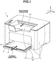
- Fig. 1 illustrates a perspective view of the image forming apparatus 1.
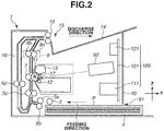
- Fig. 2 illustrates a cross-sectional view of the image forming apparatus 1 along a plane perpendicular to the X-direction (the rotational axis direction of the photosensitive drum 11).
- the image forming apparatus 1 includes a feeding cassette 4 in which recording materials P are stored, and a discharge tray 14 in which a discharged recording material P is stacked.
- the feeding cassette 4 is inserted through a feeding opening 81, and thus the recording materials P stored in the feeding cassette 4 can be fed to the inside of the image forming apparatus 1.
- the feeding cassette 4 can be pulled out in the Y-direction from the feeding opening 81, and a user can replenish recording materials P.
- a recording material P which is fed from the feeding cassette 4 and on which an image is formed is discharged in a discharge direction (the Y-axis positive direction) illustrated in Fig. 1 through a discharge opening 15 and stacked in the discharge tray 14.
- a front cover 70 is provided and covers a circuit board 100.
- an exterior cover 71 is provided in a part of the front surface other than the portion where the front cover 70 is provided and on side surfaces and a top surface of the image forming apparatus 1.
- the front cover 70, the exterior cover 71, and the discharge tray 14 form a housing 75 of the image forming apparatus 1 together.
- the housing 75 is a member covering the image forming apparatus 1 and includes process members, such as an optical box 50 inside.
- the feeding opening 81 and the discharge opening 15 are openings formed in parts of the housing 75.
- a recording material P is inserted to inside the image forming apparatus 1 through the feeding opening 81, and a recording material P is discharged to outside the image forming apparatus 1 through the discharge opening 15.
- the recording material P is fed into the image forming apparatus in a feeding direction (or predetermined direction).
- the photosensitive drum (or image bearing member) 11 that is a rotating member is rotationally driven at a predetermined peripheral velocity (a process speed) in the direction of an arrow R, based on a print start signal.
- the optical box 50 emits laser light toward the photosensitive drum 11.
- the optical box 50 is a box-shaped unit including inside members, such as a laser oscillator that outputs laser light, a polygon mirror and a lens for irradiating the photosensitive drum 11 with the laser light, and a scanner motor that rotates the polygon mirror.
- the photosensitive drum 11 is charged in advance by a charging roller 17 and is irradiated with the laser light, and thus an electrostatic latent image is formed on the photosensitive drum 11. Then, a developing roller 12 develops the electrostatic latent image with toner, and thus a toner image is formed on the photosensitive drum 11.
- a recording material P is fed from the feeding cassette 4.
- a pickup roller 3 comes into contact with a recording material P at the top of the recording materials P stored in the feeding cassette 4 and itself rotates, to feed the recording material P in a feeding direction (the Y-axis negative direction).
- the feeding roller 5a and a separation pad 5b that is in pressure contact with the feeding roller 5a form a separation nip.
- the feeding roller 5a and the separation pad 5b separate the plurality of recording materials P and feed only a recording material P at the top to the downstream side.
- the recording material P fed from the feeding cassette 4 is conveyed toward a transfer roller 7 by the conveying roller pair 5c.
- a transfer bias is applied to the transfer roller 7, to transfer the toner image formed on the photosensitive drum 11 to the recording material P.
- the recording material P to which the toner image is transferred by the transfer roller 7 is subjected to a heating/pressurization process by a fixing device 9, and thus the toner image is fixed to the recording material P.
- the fixing device 9 includes a heating roller 9a that has a built-in heater (not illustrated), and a pressure roller 9b that is biased toward the heating roller 9a. Then, the recording material P to which the toner image is fixed is discharged to the discharge tray 14 by a discharge roller pair 10.
- the discharge roller pair 10 switches back the recording material P, on a first surface of which the image is formed, to guide the recording material P to a two-sided conveying path 16.
- the recording material P guided to the two-sided conveying path 16 is conveyed toward the transfer roller 7 again by a two-sided conveying roller pair 5d.
- the recording material P is discharged to outside the image forming apparatus 1 by the discharge roller pair 10.
- toner remaining on the photosensitive drum 11 is cleaned by a cleaning unit 13.
- the image forming apparatus 1 includes the circuit board 100.
- the circuit board 100 includes a wiring board 101 made of an insulator and electronic components 111 and 121 soldered to the wiring board 101. On and inside the board of the wiring board 101, conductor wiring is provided, and thus, the electronic components 111 and 121 are electrically connected together.
- the circuit board 100 has a function of converting an alternating current supplied from outside the image forming apparatus 1 into a direct current and converting an input voltage to obtain a predetermined voltage value required for the image forming process.
- the circuit board 100 is disposed in such a direction that a surface of the wiring board 101 on which the electronic components 111 and 121 are mounted intersects the discharge direction. Further, the wiring board 101 is provided between the front cover 70 and the optical box 50 in the discharge direction. The electronic components 111 and 121 are provided on a surface of the wiring board 101 which is a surface opposite to the optical box 50.
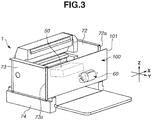
- FIG. 3 is a perspective view of the image forming apparatus 1 for illustrating the configuration of the circuit board 100.
- the front cover 70 and the exterior cover 71 are omitted (for illustration purposes).
- the circuit board 100 is installed on the front surface side.
- the optical box 50 and a driving motor 60 are provided.
- the optical box 50 and the driving motor 60 are actually at positions where the optical box 50 and the driving motor 60 cannot be seen by the user, and thus are illustrated by dotted lines.
- the image forming apparatus 1 includes a right side plate frame 72 (a first side plate frame), a left side plate frame 73 (a second side plate frame), and a base frame 74.
- the right side plate frame 72 supports an end portion on the right side (a first end portion) of the photosensitive drum 11 in the X-direction.
- the left side plate frame 73 supports an end portion on the left side (a second end portion) of the photosensitive drum 11 in the X-direction.
- the base frame 74 is provided on a bottom surface and supports the right side plate frame 72 and the left side plate frame 73 from below.
- the circuit board 100 is supported by these frame members and is mounted on the image forming apparatus 1 such that a board surface of the circuit board 100 is approximately parallel to the XZ plane.
- the right side plate frame 72 and the left side plate frame 73 are reinforced with bent portions 72a and 73a, respectively, formed in end portions in the Y-direction of the right side plate frame 72 and the left side plate frame 73.
- the bent portion 72a is bent toward the positive side in the X-direction, to be approximately parallel to the XZ plane.
- the bent portion 73a is bent toward the negative side in the X-direction, to be approximately parallel to the XZ plane. That is, the bent portions 72a and 73a are bent along the surface of the wiring board 101. Since both side plate frames are thus bent toward outside the image forming apparatus 1 (in directions away from the photosensitive drum 11 in the X-direction), electronic components can be mounted on a larger area of the wiring board 101.
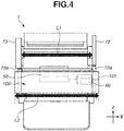
- Fig. 4 is a front perspective view of the image forming apparatus 1 for illustrating the configuration of the circuit board 100.
- a distance L1 between inner surfaces of the right side plate frame 72 and the left side plate frame 73 in the X-direction is shorter than a length L2 of the circuit board 100 in the X-direction.
- the wiring board 101 is disposed further on the positive side (the front surface side) in the Y-direction than the bent portions 72a and 73a, and the wiring board 101 is in contact with each of the bent portions 72a and 73a.
- the circuit board 100 and the bent portions 72a and 73a overlap each other.
- parts of the bent portions 72a and 73a, the optical box 50, and the driving motor 60 are actually at positions where the parts of the bent portions 72a and 73a, the optical box 50, and the driving motor 60 cannot be seen by the user, and thus are illustrated by dotted lines.
- Fig. 5 is a perspective view of the circuit board 100 when viewed from behind a main body of the image forming apparatus 1.
- the electronic components 111 which are larger in size in the Y-direction than other members, are provided together in a lower portion of the wiring board 101 and are mounted within a range below the optical box 50. More specifically, the electronic components 111 are provided below the center of the wiring board 101 in the vertical direction.
- a power source input unit 115 is provided in an end portion of the wiring board 101.
- the power source input unit 115 is connected to an inlet (not illustrated) and receives supply of power from a commercial power source.
- Fig. 6 is an enlarged cross-sectional view of the circuit board 100 when viewed from a left side surface of the main body.
- the optical box 50 is disposed at an optimal position for emitting laser light indicated by a chain line to the photosensitive drum 11.
- a member protruding greatly from the board surface, such as the electronic components 111 is not disposed. That is, the optical box 50 and the electronic components 111 are disposed at positions shifted from each other in the Z-direction, to avoid interference with each other.
- Fig. 7 is an enlarged top view of the circuit board 100 when viewed from an upper surface of the main body.
- the optical box 50 and the electronic components 111 are disposed at positions where the optical box 50 and the electronic components 111 partially overlap each other.
- the electronic components 111 are illustrated in a see-through manner by indicating the optical box 50 by a dotted line.
- the electronic components 111 are thus disposed at the above-described position, whereby it is possible to shorten the distance in the Y-direction (the front-back direction) between the circuit board 100 and the optical box 50. Thus, it is possible to downsize the image forming apparatus 1.
- the driving motor 60 functions to rotate members (the pickup roller 3, the feeding roller 5a, and the conveying roller pair 5c) for feeding and conveying a recording material P and also rotate the photosensitive drum 11.
- the driving motor 60 protrudes to the negative side in the X-direction, and the wiring board 101 is disposed on the front side of the main body with respect to the driving motor 60.
- the electronic components 111 are mounted at positions shifted from the driving motor 60, to avoid interference with the driving motor 60.
- the driving motor 60 and the electronic components 111 are disposed at positions where the driving motor 60 and the electronic components 111 partially overlap each other.
- the driving motor 60 and the electronic components 111 are disposed at positions shifted from each other in the X-direction, to avoid interference with each other.
- the electronic components 111 are thus disposed at the above-described position, whereby it is possible to shorten the distance in the Y-direction (the front-back direction) between the circuit board 100 and the driving motor 60. Thus, it is possible to downsize the image forming apparatus 1.
- FIG. 8 is a diagram obtained by additionally illustrating the right side plate frame 72 and a scanner holding member 40 to the perspective view in Fig. 5 .
- the left side plate frame 73 and the base frame 74 are omitted (for illustration purposes).
- the optical box 50 is held by the scanner holding member 40.
- the scanner holding member 40 is fixed to each of the right side plate frame 72 and the left side plate frame 73 (not illustrated in Fig. 8 ) and configured to bridge the two frames.
- the driving motor 60 is attached to the right side plate frame 72, and a gear coupled to the driving motor 60 is provided on the positive side (the right side) in the X-direction of the right side plate frame 72.
- the driving force of the driving motor 60 is transmitted to the feeding roller 5a and the photosensitive drum 11 via this gear.
- Fig. 9 is a rear view of the circuit board 100 when viewed from the back side of the main body.
- Fig. 9 illustrates not only the circuit board 100, and also the optical box 50 and the driving motor 60.
- the circuit board 100 includes a low-voltage power source unit 110 that introduces alternating current power from an external commercial power source and converts the alternating current power into direct current power, and a high-voltage power source unit 120 that supplies a high voltage required for the image formation to the process members.
- the low-voltage power source unit 110 and the high-voltage power source unit 120 are mounted on the same board.
- the low-voltage power source unit 110 includes, as the electronic components 111 that are large in size in the Y-direction, a low-voltage power source transformer 112, a heat sink 113, and an electrolytic capacitor 114. Further, the low-voltage power source unit 110 includes the power source input unit 115.
- the high-voltage power source unit 120 includes, as the electronic components 121 that are large in size in the Y-direction, a charging transformer 122, a developing transformer 123, and a transfer transformer 124. As is clear from Fig. 9 , the electronic components 111 and 121 that are large in size in the Y-direction are both disposed at positions shifted from the positions of the optical box 50 and the driving motor 60.
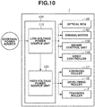
- Fig. 10 is a block diagram illustrating a function of the circuit board 100.
- the low-voltage power source unit 110 introduces power from an external power source via the power source input unit 115 mounted on an end portion of the circuit board 100 and converts an alternating current voltage into a stable direct current voltage using a rectification smoothing circuit including the electrolytic capacitor 114. Then, the low-voltage power source unit 110 converts the direct current voltage into a high-frequency alternating current voltage using a switching element, such as a transistor and then inputs the high-frequency alternating current voltage to the low-voltage power source transformer 112. The low-voltage power source transformer 112 converts the high-frequency alternating current voltage as an input voltage into an alternating current voltage (an output voltage) having a desired voltage value.
- a switching element such as a transistor
- the low-voltage power source unit 110 converts the alternating current voltage into a direct current voltage again and outputs the obtained direct current voltage to the high-voltage power source unit 120 and the optical box 50.
- losses of individual circuit components appear as heat.
- the heat sink 113 made of aluminum or iron is provided.
- the high-voltage power source unit 120 converts the voltage (e.g., 24 V) supplied from the low-voltage power source unit 110 into a high voltage required for the image forming process, such as charging, development, and transfer.
- the charging transformer 122 converts the voltage supplied from the low-voltage power source unit 110 into a voltage for charging, and then, the converted voltage is supplied to the charging roller 17.
- the developing transformer 123 converts the voltage supplied from the low-voltage power source unit 110 into a voltage for development, and then, the converted voltage is supplied to the developing roller 12.
- the transfer transformer 124 converts the voltage supplied from the low-voltage power source unit 110 into a voltage for transfer, and then, the converted voltage is supplied to the transfer roller 7.
- the low-voltage power source unit 110 supplies a voltage (e.g., 3.3 V or 5 V) to not only the high-voltage power source unit 120, but also the optical box 50, the driving motor 60, an engine control unit 130, and a video controller 140.
- the engine control unit 130 functions to perform overall control of the various process members.
- the engine control unit 130 includes a central processing unit (CPU) (not illustrated), a random-access memory (RAM) (not illustrated) that is used to calculate or temporarily store data required to control the image forming apparatus 1, and a read-only memory (ROM) (not illustrated) that stores a program for controlling the image forming apparatus 1 and various types of data.
- CPU central processing unit
- RAM random-access memory
- ROM read-only memory
- the engine control unit 130 may be provided on a different board from the circuit board 100, or may be provided on the same board as the circuit board 100.
- the video controller 140 functions to communicate with an external device, such as a personal computer, receive print data, and notify the engine control unit 130 of a result of analyzing the print data.
- the low-voltage power source unit 110 and the high-voltage power source unit 120 are provided on the same board (the circuit board 100).
- the present invention is not limited to this.
- the two power source units may be provided on different boards. Both the board of the low-voltage power source unit 110 and the board of the high-voltage power source unit 120 may be provided on the front surface side of the image forming apparatus 1 illustrated in Fig. 3 . Alternatively, only the board of the low-voltage power source unit 110 may be provided on the front surface side, and the board of the high-voltage power source unit 120 may be provided at a different position.
- the board of the high-voltage power source unit 120 may be provided on the front surface side, and the board of the low-voltage power source unit 110 may be provided at a different position. In this case, however, it is desirable that the electronic components 121 that are large in size in the Y-direction and are mounted on the high-voltage power source unit 120 should be disposed at positions shifted from the positions of the optical box 50 and the driving motor 60.
- the distance L1 between the inner surfaces of the right side plate frame 72 and the left side plate frame 73 in the X-direction is shorter than the length L2 of the circuit board 100 in the X-direction.
- the present invention is not limited to this configuration.
- the relationship may be such that the distance L1 is greater than or equal to the length L2.
- the wiring board 101 may be provided further on the negative side (the back surface side) in the Y-direction than the bent portions 72a and 73a. That is, the wiring board 101 may be provided in an area between the inner surfaces of the right side plate frame 72 and the left side plate frame 73.
- a part of the low-voltage power source unit 110 is mounted.
- the present invention is not limited to this.
- a different circuit, such as the high-voltage power source unit 120, may be mounted, or the circuit board 100 may not be mounted at this position in the first place.
- the feeding cassette 4 that can be pulled out of the main body of the image forming apparatus 1.
- the present invention is not limited to this configuration.
- a tray that cannot be pulled out of the image forming apparatus 1 and allows the user to directly insert a recording material P through the feeding opening 81 formed in front of the image forming apparatus 1 may be used.
- the front cover 70 is provided on the same side (the front surface side) as the side where the feeding opening 81 is provided.
- the feeding direction and the discharge direction are opposite to each other, but are in a parallel relationship.
- the front cover 70 is located upstream of the optical box 50 in the feeding direction.
- the optical box 50 and the electronic components 111 have the relationship where, when viewed in the vertical direction, the optical box 50 and the electronic components 111 at least partially overlap each other.
- the present invention is not limited to this.
- the optical box 50 and the electronic components 111 may be disposed at positions shifted from each other to some extent in the X-direction. That is, the optical box 50 and the electronic components 111 may have the relationship where, when viewed in the vertical direction, the optical box 50 and the electronic components 111 do not overlap each other, but when viewed in a direction parallel to the XZ plane and intersecting the vertical direction, the optical box 50 and the electronic components 111 at least partially overlap each other.
- the optical box 50 and the electronic components 111 may have the relationship where, when viewed in a direction orthogonal to the discharge direction or the feeding direction, the optical box 50 and the electronic components 111 at least partially overlap each other. Even with the above configuration, the distance in the Y-direction (the front-back direction) between the circuit board 100 and the optical box 50 can be shortened, and thus it is possible to downsize the image forming apparatus 1.
Landscapes
- Physics & Mathematics (AREA)
- General Physics & Mathematics (AREA)
- Optics & Photonics (AREA)
- Electrophotography Configuration And Component (AREA)
- Studio Devices (AREA)
- Accessory Devices And Overall Control Thereof (AREA)
Abstract
Description
- The present invention relates to an image forming apparatus that forms an image on a recording material.
- Inside an image forming apparatus, such as a printer or a copying machine, many components, such as a circuit board and a motor, are mounted. The publication of
Japanese Patent Application Laid-Open No. 2016-20932 - The configuration discussed in the publication of
Japanese Patent Application Laid-Open No. 2016-20932 - The present invention is directed to meeting further user demand.
- According to a first aspect of the present invention, there is provided an image forming apparatus as specified in claims 1 to 8. According to a second aspect of the present invention, there is provided an image forming apparatus as specified in claims 9 to 13. According to a third aspect of the present invention, there is provided an image forming apparatus as specified in
claims - Further features of the present invention will become apparent from the following description of exemplary embodiments with reference to the attached drawings.
-
-
Fig. 1 is a perspective view of an image forming apparatus. -
Fig. 2 is a cross-sectional view of the image forming apparatus. -
Fig. 3 is a perspective view for illustrating a position of a circuit board. -
Fig. 4 is a front perspective view for illustrating the position of the circuit board. -
Fig. 5 is a perspective view of the circuit board and peripheral members of the circuit board. -
Fig. 6 is a cross-sectional view of the circuit board and the peripheral members of the circuit board. -
Fig. 7 is a top view of the circuit board and the peripheral members of the circuit board. -
Fig. 8 is a perspective view for illustrating a holding configuration of an optical box and a driving motor. -
Fig. 9 is a diagram illustrating electronic components on the circuit board. -
Fig. 10 is a block diagram illustrating a function of the circuit board. - With reference to the drawings, an exemplary embodiment for carrying out this invention will be described in detail in an illustrative manner based on exemplary embodiments below. However, the dimensions, the materials, the shapes, and the relative arrangement of components described in this exemplary embodiment should be appropriately changed according to the configuration of an apparatus to which the invention is applied, or various conditions. That is, the scope of the invention is not limited to the following exemplary embodiment. Each of the embodiments of the present invention described below can be implemented solely or as a combination of a plurality of the embodiments or features thereof where necessary or where the combination of elements or features from individual embodiments in a single embodiment is beneficial.
- The overall configuration of an image forming apparatus 1 according to the present exemplary embodiment is described. The image forming apparatus 1 according to the present exemplary embodiment is a monochrome laser beam printer using an electrophotographic process and forms an image on a recording material P using a developer (toner) according to image information transmitted from an external device, such as a personal computer. Examples of the recording material P include a recording sheet, a label sheet, an overhead projector (OHP) sheet, and cloth.
- In the following description, the height direction (a direction opposite to a vertical direction) of the image forming apparatus 1 in a case where the image forming apparatus 1 is installed on a horizontal surface is a Z-direction. A direction intersecting the Z-direction and parallel to the axis direction (a main scanning direction) of a
photosensitive drum 11 is an X-direction. A direction intersecting the X-direction and the Z-direction is a Y-direction. It is desirable that the X-direction, the Y-direction, and the Z-direction should perpendicularly intersect each other. For convenience, the positive side in the X-direction is referred to as a "right side", and the negative side in the X-direction is referred to as a "left side". The positive side in the Y-direction is referred to as a "front side" or a "front surface side", and the negative side in the Y-direction is referred to as a "back side" or a "back surface side". The positive side in the Z-direction is referred to as an "upper side", and the negative side in the Z-direction is referred to as a "lower side". -
Fig. 1 illustrates a perspective view of the image forming apparatus 1.Fig. 2 illustrates a cross-sectional view of the image forming apparatus 1 along a plane perpendicular to the X-direction (the rotational axis direction of the photosensitive drum 11). InFig. 1 , the image forming apparatus 1 includes afeeding cassette 4 in which recording materials P are stored, and adischarge tray 14 in which a discharged recording material P is stacked. Thefeeding cassette 4 is inserted through afeeding opening 81, and thus the recording materials P stored in thefeeding cassette 4 can be fed to the inside of the image forming apparatus 1. Thefeeding cassette 4 can be pulled out in the Y-direction from thefeeding opening 81, and a user can replenish recording materials P. A recording material P which is fed from thefeeding cassette 4 and on which an image is formed is discharged in a discharge direction (the Y-axis positive direction) illustrated inFig. 1 through adischarge opening 15 and stacked in thedischarge tray 14. - In a part of the side surface (a part of a front surface) of the image forming apparatus 1 on the downstream side in the discharge direction, a
front cover 70 is provided and covers acircuit board 100. In a part of the front surface other than the portion where thefront cover 70 is provided and on side surfaces and a top surface of the image forming apparatus 1, anexterior cover 71 is provided. Thefront cover 70, theexterior cover 71, and the discharge tray 14 form ahousing 75 of the image forming apparatus 1 together. Thehousing 75 is a member covering the image forming apparatus 1 and includes process members, such as anoptical box 50 inside. The feeding opening 81 and thedischarge opening 15 are openings formed in parts of thehousing 75. A recording material P is inserted to inside the image forming apparatus 1 through thefeeding opening 81, and a recording material P is discharged to outside the image forming apparatus 1 through thedischarge opening 15. The recording material P is fed into the image forming apparatus in a feeding direction (or predetermined direction). - With reference to the cross-sectional view in
Fig. 2 , the procedure of an image forming operation on a recording material P is described. In response to transmission of image information to the image forming apparatus 1, the photosensitive drum (or image bearing member) 11 that is a rotating member is rotationally driven at a predetermined peripheral velocity (a process speed) in the direction of an arrow R, based on a print start signal. Based on the input image information, theoptical box 50 emits laser light toward thephotosensitive drum 11. Theoptical box 50 is a box-shaped unit including inside members, such as a laser oscillator that outputs laser light, a polygon mirror and a lens for irradiating thephotosensitive drum 11 with the laser light, and a scanner motor that rotates the polygon mirror. Thephotosensitive drum 11 is charged in advance by acharging roller 17 and is irradiated with the laser light, and thus an electrostatic latent image is formed on thephotosensitive drum 11. Then, a developingroller 12 develops the electrostatic latent image with toner, and thus a toner image is formed on thephotosensitive drum 11. - In parallel with the above described image forming process, a recording material P is fed from the
feeding cassette 4. On a conveying path of the image forming apparatus 1, apickup roller 3, afeeding roller 5a, and a conveyingroller pair 5c are provided. The pickup roller 3 (a feeding member) comes into contact with a recording material P at the top of the recording materials P stored in thefeeding cassette 4 and itself rotates, to feed the recording material P in a feeding direction (the Y-axis negative direction). Thefeeding roller 5a and aseparation pad 5b that is in pressure contact with thefeeding roller 5a form a separation nip. In a case where a plurality of recording materials P is fed to the separation nip by a frictional force between recording materials P, thefeeding roller 5a and theseparation pad 5b separate the plurality of recording materials P and feed only a recording material P at the top to the downstream side. - The recording material P fed from the
feeding cassette 4 is conveyed toward atransfer roller 7 by the conveyingroller pair 5c. A transfer bias is applied to thetransfer roller 7, to transfer the toner image formed on thephotosensitive drum 11 to the recording material P. The recording material P to which the toner image is transferred by thetransfer roller 7 is subjected to a heating/pressurization process by a fixing device 9, and thus the toner image is fixed to the recording material P. The fixing device 9 includes aheating roller 9a that has a built-in heater (not illustrated), and apressure roller 9b that is biased toward theheating roller 9a. Then, the recording material P to which the toner image is fixed is discharged to thedischarge tray 14 by adischarge roller pair 10. - In a case where images are formed on both sides of the recording material P, the
discharge roller pair 10 switches back the recording material P, on a first surface of which the image is formed, to guide the recording material P to a two-sided conveyingpath 16. The recording material P guided to the two-sided conveyingpath 16 is conveyed toward thetransfer roller 7 again by a two-sided conveyingroller pair 5d. After an image is formed on a second surface of the recording material P by thetransfer roller 7, the recording material P is discharged to outside the image forming apparatus 1 by thedischarge roller pair 10. After the toner image is transferred to the recording material P, toner remaining on thephotosensitive drum 11 is cleaned by acleaning unit 13. - As illustrated in
Fig. 2 , the image forming apparatus 1 includes thecircuit board 100. Thecircuit board 100 includes awiring board 101 made of an insulator andelectronic components wiring board 101. On and inside the board of thewiring board 101, conductor wiring is provided, and thus, theelectronic components circuit board 100 has a function of converting an alternating current supplied from outside the image forming apparatus 1 into a direct current and converting an input voltage to obtain a predetermined voltage value required for the image forming process. - As illustrated in
Fig. 2 , thecircuit board 100 is disposed in such a direction that a surface of thewiring board 101 on which theelectronic components wiring board 101 is provided between thefront cover 70 and theoptical box 50 in the discharge direction. Theelectronic components wiring board 101 which is a surface opposite to theoptical box 50. - With reference to
Figs. 3 to 8 , a configuration of thecircuit board 100 according to the present exemplary embodiment is described in detail.Fig. 3 is a perspective view of the image forming apparatus 1 for illustrating the configuration of thecircuit board 100. InFig. 3 , unlikeFig. 1 , thefront cover 70 and theexterior cover 71 are omitted (for illustration purposes). As illustrated inFig. 3 , thecircuit board 100 is installed on the front surface side. Further on the back side of the circuit board 100 (the negative side in the Y-direction), theoptical box 50 and a drivingmotor 60 are provided. InFig. 3 , theoptical box 50 and the drivingmotor 60 are actually at positions where theoptical box 50 and the drivingmotor 60 cannot be seen by the user, and thus are illustrated by dotted lines. - As illustrated in
Fig. 3 , the image forming apparatus 1 includes a right side plate frame 72 (a first side plate frame), a left side plate frame 73 (a second side plate frame), and abase frame 74. The rightside plate frame 72 supports an end portion on the right side (a first end portion) of thephotosensitive drum 11 in the X-direction. The leftside plate frame 73 supports an end portion on the left side (a second end portion) of thephotosensitive drum 11 in the X-direction. Thebase frame 74 is provided on a bottom surface and supports the rightside plate frame 72 and the leftside plate frame 73 from below. - The
circuit board 100 is supported by these frame members and is mounted on the image forming apparatus 1 such that a board surface of thecircuit board 100 is approximately parallel to the XZ plane. The rightside plate frame 72 and the leftside plate frame 73 are reinforced withbent portions side plate frame 72 and the leftside plate frame 73. Thebent portion 72a is bent toward the positive side in the X-direction, to be approximately parallel to the XZ plane. Thebent portion 73a is bent toward the negative side in the X-direction, to be approximately parallel to the XZ plane. That is, thebent portions wiring board 101. Since both side plate frames are thus bent toward outside the image forming apparatus 1 (in directions away from thephotosensitive drum 11 in the X-direction), electronic components can be mounted on a larger area of thewiring board 101. -
Fig. 4 is a front perspective view of the image forming apparatus 1 for illustrating the configuration of thecircuit board 100. As illustrated inFig. 4 , a distance L1 between inner surfaces of the rightside plate frame 72 and the leftside plate frame 73 in the X-direction is shorter than a length L2 of thecircuit board 100 in the X-direction. Thewiring board 101 is disposed further on the positive side (the front surface side) in the Y-direction than thebent portions wiring board 101 is in contact with each of thebent portions circuit board 100 and thebent portions Fig. 4 , parts of thebent portions optical box 50, and the drivingmotor 60 are actually at positions where the parts of thebent portions optical box 50, and the drivingmotor 60 cannot be seen by the user, and thus are illustrated by dotted lines. - Next, with reference to
Figs. 5 to 7 , the positional relationship between theelectronic components 111 and theoptical box 50 is described in detail. -
Fig. 5 is a perspective view of thecircuit board 100 when viewed from behind a main body of the image forming apparatus 1. To effectively utilize space, theelectronic components 111, which are larger in size in the Y-direction than other members, are provided together in a lower portion of thewiring board 101 and are mounted within a range below theoptical box 50. More specifically, theelectronic components 111 are provided below the center of thewiring board 101 in the vertical direction. In an end portion of thewiring board 101, a powersource input unit 115 is provided. The powersource input unit 115 is connected to an inlet (not illustrated) and receives supply of power from a commercial power source. -
Fig. 6 is an enlarged cross-sectional view of thecircuit board 100 when viewed from a left side surface of the main body. Theoptical box 50 is disposed at an optimal position for emitting laser light indicated by a chain line to thephotosensitive drum 11. In a portion where theoptical box 50 and thewiring board 101 are closest to each other in the Y-direction, a member protruding greatly from the board surface, such as theelectronic components 111, is not disposed. That is, theoptical box 50 and theelectronic components 111 are disposed at positions shifted from each other in the Z-direction, to avoid interference with each other. -
Fig. 7 is an enlarged top view of thecircuit board 100 when viewed from an upper surface of the main body. InFig. 7 , theoptical box 50 and theelectronic components 111 are disposed at positions where theoptical box 50 and theelectronic components 111 partially overlap each other. As described above, since theoptical box 50 is provided above theelectronic components 111, normally, theelectronic components 111 cannot be seen from this direction. InFig. 7 , to illustrate the positional relationship between theoptical box 50 and theelectronic components 111 in an easily understandable manner, theelectronic components 111 are illustrated in a see-through manner by indicating theoptical box 50 by a dotted line. - The
electronic components 111 are thus disposed at the above-described position, whereby it is possible to shorten the distance in the Y-direction (the front-back direction) between thecircuit board 100 and theoptical box 50. Thus, it is possible to downsize the image forming apparatus 1. - Next, with reference to
Figs. 5 and7 , the positional relationship between theelectronic components 111 and the drivingmotor 60 is described in detail. The drivingmotor 60 functions to rotate members (thepickup roller 3, the feedingroller 5a, and the conveyingroller pair 5c) for feeding and conveying a recording material P and also rotate thephotosensitive drum 11. - As illustrated in
Fig. 5 , the drivingmotor 60 protrudes to the negative side in the X-direction, and thewiring board 101 is disposed on the front side of the main body with respect to the drivingmotor 60. It is understood that theelectronic components 111 are mounted at positions shifted from the drivingmotor 60, to avoid interference with the drivingmotor 60. As illustrated inFig. 6 , when viewed from the left side surface of the main body, the drivingmotor 60 and theelectronic components 111 are disposed at positions where the drivingmotor 60 and theelectronic components 111 partially overlap each other. As illustrated inFig. 7 , when viewed from the upper surface of the main body, the drivingmotor 60 and theelectronic components 111 are disposed at positions shifted from each other in the X-direction, to avoid interference with each other. - The
electronic components 111 are thus disposed at the above-described position, whereby it is possible to shorten the distance in the Y-direction (the front-back direction) between thecircuit board 100 and the drivingmotor 60. Thus, it is possible to downsize the image forming apparatus 1. - Next, with reference to
Fig. 8 , an attachment configuration of theoptical box 50 and the drivingmotor 60 to the main body is described in detail.Fig. 8 is a diagram obtained by additionally illustrating the rightside plate frame 72 and ascanner holding member 40 to the perspective view inFig. 5 . The leftside plate frame 73 and thebase frame 74 are omitted (for illustration purposes). - The
optical box 50 is held by thescanner holding member 40. Thescanner holding member 40 is fixed to each of the rightside plate frame 72 and the left side plate frame 73 (not illustrated inFig. 8 ) and configured to bridge the two frames. The drivingmotor 60 is attached to the rightside plate frame 72, and a gear coupled to the drivingmotor 60 is provided on the positive side (the right side) in the X-direction of the rightside plate frame 72. The driving force of the drivingmotor 60 is transmitted to thefeeding roller 5a and thephotosensitive drum 11 via this gear. - Next, with reference to
Fig. 9 , a configuration of thecircuit board 100 is described.Fig. 9 is a rear view of thecircuit board 100 when viewed from the back side of the main body.Fig. 9 illustrates not only thecircuit board 100, and also theoptical box 50 and the drivingmotor 60. - The
circuit board 100 includes a low-voltagepower source unit 110 that introduces alternating current power from an external commercial power source and converts the alternating current power into direct current power, and a high-voltagepower source unit 120 that supplies a high voltage required for the image formation to the process members. In thecircuit board 100 according to the present exemplary embodiment, the low-voltagepower source unit 110 and the high-voltagepower source unit 120 are mounted on the same board. - The low-voltage
power source unit 110 includes, as theelectronic components 111 that are large in size in the Y-direction, a low-voltagepower source transformer 112, aheat sink 113, and anelectrolytic capacitor 114. Further, the low-voltagepower source unit 110 includes the powersource input unit 115. The high-voltagepower source unit 120 includes, as theelectronic components 121 that are large in size in the Y-direction, a chargingtransformer 122, a developingtransformer 123, and atransfer transformer 124. As is clear fromFig. 9 , theelectronic components optical box 50 and the drivingmotor 60. - Next, with reference to
Figs. 9 and10 , functions of the low-voltagepower source unit 110 and the high-voltagepower source unit 120 are described.Fig. 10 is a block diagram illustrating a function of thecircuit board 100. - First, the low-voltage
power source unit 110 introduces power from an external power source via the powersource input unit 115 mounted on an end portion of thecircuit board 100 and converts an alternating current voltage into a stable direct current voltage using a rectification smoothing circuit including theelectrolytic capacitor 114. Then, the low-voltagepower source unit 110 converts the direct current voltage into a high-frequency alternating current voltage using a switching element, such as a transistor and then inputs the high-frequency alternating current voltage to the low-voltagepower source transformer 112. The low-voltagepower source transformer 112 converts the high-frequency alternating current voltage as an input voltage into an alternating current voltage (an output voltage) having a desired voltage value. The low-voltagepower source unit 110 converts the alternating current voltage into a direct current voltage again and outputs the obtained direct current voltage to the high-voltagepower source unit 120 and theoptical box 50. In the low-voltagepower source unit 110, losses of individual circuit components appear as heat. Thus, to dissipate the heat, theheat sink 113 made of aluminum or iron is provided. - The high-voltage
power source unit 120 converts the voltage (e.g., 24 V) supplied from the low-voltagepower source unit 110 into a high voltage required for the image forming process, such as charging, development, and transfer. The chargingtransformer 122 converts the voltage supplied from the low-voltagepower source unit 110 into a voltage for charging, and then, the converted voltage is supplied to the chargingroller 17. The developingtransformer 123 converts the voltage supplied from the low-voltagepower source unit 110 into a voltage for development, and then, the converted voltage is supplied to the developingroller 12. Thetransfer transformer 124 converts the voltage supplied from the low-voltagepower source unit 110 into a voltage for transfer, and then, the converted voltage is supplied to thetransfer roller 7. - The low-voltage
power source unit 110 supplies a voltage (e.g., 3.3 V or 5 V) to not only the high-voltagepower source unit 120, but also theoptical box 50, the drivingmotor 60, anengine control unit 130, and avideo controller 140. Theengine control unit 130 functions to perform overall control of the various process members. Theengine control unit 130 includes a central processing unit (CPU) (not illustrated), a random-access memory (RAM) (not illustrated) that is used to calculate or temporarily store data required to control the image forming apparatus 1, and a read-only memory (ROM) (not illustrated) that stores a program for controlling the image forming apparatus 1 and various types of data. Theengine control unit 130 may be provided on a different board from thecircuit board 100, or may be provided on the same board as thecircuit board 100. Thevideo controller 140 functions to communicate with an external device, such as a personal computer, receive print data, and notify theengine control unit 130 of a result of analyzing the print data. - Based on the above-described configuration, according to the present exemplary embodiment, it is possible to meet further user demand.
- In the above exemplary embodiment, a description has been given of a configuration in which the low-voltage
power source unit 110 and the high-voltagepower source unit 120 are provided on the same board (the circuit board 100). The present invention, however, is not limited to this. The two power source units may be provided on different boards. Both the board of the low-voltagepower source unit 110 and the board of the high-voltagepower source unit 120 may be provided on the front surface side of the image forming apparatus 1 illustrated inFig. 3 . Alternatively, only the board of the low-voltagepower source unit 110 may be provided on the front surface side, and the board of the high-voltagepower source unit 120 may be provided at a different position. - Yet alternatively, only the board of the high-voltage
power source unit 120 may be provided on the front surface side, and the board of the low-voltagepower source unit 110 may be provided at a different position. In this case, however, it is desirable that theelectronic components 121 that are large in size in the Y-direction and are mounted on the high-voltagepower source unit 120 should be disposed at positions shifted from the positions of theoptical box 50 and the drivingmotor 60. - In the above exemplary embodiment, a description has been given of a configuration in which, as illustrated in
Fig. 4 , the distance L1 between the inner surfaces of the rightside plate frame 72 and the leftside plate frame 73 in the X-direction is shorter than the length L2 of thecircuit board 100 in the X-direction. The present invention, however, is not limited to this configuration. For example, the relationship may be such that the distance L1 is greater than or equal to the length L2. Also, thewiring board 101 may be provided further on the negative side (the back surface side) in the Y-direction than thebent portions wiring board 101 may be provided in an area between the inner surfaces of the rightside plate frame 72 and the leftside plate frame 73. - In the above exemplary embodiment, as illustrated in
Fig. 9 , at a position overlapping theoptical box 50 when viewed from a back surface of the main body (a position opposed to theoptical box 50 in the Y-direction), a part of the low-voltagepower source unit 110 is mounted. The present invention, however, is not limited to this. A different circuit, such as the high-voltagepower source unit 120, may be mounted, or thecircuit board 100 may not be mounted at this position in the first place. - In the above exemplary embodiment, a description has been given using as an example the feeding
cassette 4 that can be pulled out of the main body of the image forming apparatus 1. The present invention, however, is not limited to this configuration. A tray that cannot be pulled out of the image forming apparatus 1 and allows the user to directly insert a recording material P through thefeeding opening 81 formed in front of the image forming apparatus 1 may be used. - Further, as is clear from
Figs. 1 and2 , thefront cover 70 is provided on the same side (the front surface side) as the side where thefeeding opening 81 is provided. In the configuration of the present exemplary embodiment, the feeding direction and the discharge direction are opposite to each other, but are in a parallel relationship. Thus, it can also be said that thefront cover 70 is located upstream of theoptical box 50 in the feeding direction. - In the above exemplary embodiment, as illustrated in
Fig. 7 , theoptical box 50 and theelectronic components 111 have the relationship where, when viewed in the vertical direction, theoptical box 50 and theelectronic components 111 at least partially overlap each other. The present invention, however, is not limited to this. Theoptical box 50 and theelectronic components 111 may be disposed at positions shifted from each other to some extent in the X-direction. That is, theoptical box 50 and theelectronic components 111 may have the relationship where, when viewed in the vertical direction, theoptical box 50 and theelectronic components 111 do not overlap each other, but when viewed in a direction parallel to the XZ plane and intersecting the vertical direction, theoptical box 50 and theelectronic components 111 at least partially overlap each other. In other words, theoptical box 50 and theelectronic components 111 may have the relationship where, when viewed in a direction orthogonal to the discharge direction or the feeding direction, theoptical box 50 and theelectronic components 111 at least partially overlap each other. Even with the above configuration, the distance in the Y-direction (the front-back direction) between thecircuit board 100 and theoptical box 50 can be shortened, and thus it is possible to downsize the image forming apparatus 1. - While the present invention has been described with reference to exemplary embodiments, it is to be understood that the invention is not limited to the disclosed exemplary embodiments. The scope of the following claims is to be accorded the broadest interpretation so as to encompass all such modifications and equivalent structures and functions.
Claims (15)
- An image forming apparatus (1) comprising:an optical box (50) including a light source for emitting light to an image bearing member (11);a housing (75) including the optical box (50) inside and having a discharge opening (15) through which a recording material (P) is discharged;a cover (70) provided on an end surface of the housing (75) on a downstream side in a discharge direction in which the recording material (P) is discharged through the discharge opening (15) formed in the housing (75), disposed downstream of the optical box (50) in the discharge direction, and forming a part of the housing (75); anda circuit board (100) for converting an alternating current supplied from an external power source into a direct current and supply power to the light source,wherein the circuit board (100) includes a plurality of electronic components (111, 121) and a wiring board (101) for electrically connecting the plurality of electronic components (111, 121), the circuit board (100) is disposed in such a direction that a surface of the wiring board on which the plurality of electronic components (111, 121) is mounted intersects the discharge direction, and the wiring board (101) is provided between the cover (70) and the optical box (50) in the discharge direction, andwherein, when viewed in a vertical direction, the optical box (50) and the plurality of electronic components (111, 121) partially overlap each other.
- The image forming apparatus according to claim 1, further comprising:a motor (60) for rotationally driving the image bearing member (11), wherein, when viewed in a direction of a rotational axis of the image bearing member (11), the motor (60) and the plurality of electronic components (111, 121) partially overlap each other.
- The image forming apparatus according to claim 2, wherein, when viewed in the vertical direction, the motor (60) and the plurality of electronic components (111, 121) do not overlap each other.
- The image forming apparatus according to claim 1, further comprising:a first side plate frame (75) for supporting a first end portion of the image bearing member in a direction of a rotational axis of the image bearing member (11); anda second side plate frame (73) for supporting a second end portion of the image bearing member in the direction of the rotational axis (11),wherein a width (L2) of the circuit board (100) in the direction of the rotational axis is longer than a distance (LI) between the first side plate frame (75) and the second side plate frame (73) in the direction of the rotational axis.
- The image forming apparatus according to claim 4, wherein the first side plate frame (72) includes a first bent portion (72a) bent along the surface of the wiring board (101), the second side plate frame (73) includes a second bent portion (73a) bent along the surface of the wiring board (101), and the first bent portion (72a) and the second bent portion (73a) are in contact with the wiring board (101).
- The image forming apparatus according to claim 5, wherein the first bent portion (72a) and the second bent portion (73a) are bent in directions away from the image bearing member in the direction of the rotational axis.
- The image forming apparatus according to claim 1, wherein the plurality of electronic components (111, 121) is provided below a center of the wiring board (101) in the vertical direction.
- The image forming apparatus according to claim 1, wherein the plurality of electronic components (111, 121) includes at least any one of a capacitor (114), a transformer (112), and a heat sink (113), the capacitor (114) being for smoothing an alternating current voltage supplied from the external power source, the transformer (112) being for converting an input voltage smoothed by the capacitor (114) and converted into an alternating current voltage again by a switching element into an output voltage to be supplied to the optical box (50), the heat sink (113) being provided to dissipate heat of the circuit board (100).
- An image forming apparatus (1) comprising:an optical box (50) including a light source for emitting light to an image bearing member (11);a housing (75) including the optical box (50) inside and having an opening (81) through which a recording material (P) is inserted;a feeding member (3) for feeding the recording material (P) inserted through the opening (81) in a feeding direction;a cover (70) provided on an end surface of the housing (75) on a same side as a side where the opening (81) is formed, disposed upstream of the optical box (50) in the feeding direction, and forming a part of the housing (75); anda circuit board (100) for converting an alternating current supplied from an external power source into a direct current and supply power to the light source,wherein the circuit board (100) includes a plurality of electronic components (111, 121) and a wiring board (101) for electrically connecting the plurality of electronic components (111, 121), the circuit board (100) is disposed in such a direction that a surface of the wiring board (101) on which the plurality of electronic components (111, 121) is mounted intersects the feeding direction, and the wiring board (101) is provided between the cover (70) and the optical box (50) in the feeding direction.
- The image forming apparatus according to claim 9, further comprising:a motor (60) for rotationally driving the image bearing member (11), wherein, when viewed in a direction of a rotational axis of the image bearing member (11), the motor (60) and the plurality of electronic components (111, 121) partially overlap each other.
- The image forming apparatus according to claim 10, wherein, when viewed in a vertical direction, the motor (60) and the plurality of electronic components (111, 121) do not overlap each other.
- The image forming apparatus according to claim 9, wherein the plurality of electronic components (111, 121) is provided below a center of the wiring board (101) in a vertical direction.
- The image forming apparatus according to claim 9, wherein the plurality of electronic components (111, 121) includes at least any one of a capacitor (114), a transformer (112), and a heat sink (113), the capacitor (114) being for smoothing an alternating current voltage supplied from the external power source, the transformer (112) being for converting an input voltage smoothed by the capacitor and converted into an alternating current voltage again by a switching element into an output voltage to be supplied to the optical box, the heat sink (113) provided to dissipate heat of the circuit board.
- An image forming apparatus (1) comprising:an optical box (50) including a light source for emitting light to an image bearing member (11);a housing (75) including the optical box (50) inside and having a discharge opening (15) through which a recording material (P) is discharged; anda circuit board (100) for converting an alternating current supplied from an external power source into a direct current and supply power to the light source,wherein the circuit board (100) includes a plurality of electronic components (111, 121) and a wiring board (101) for electrically connecting the plurality of electronic components (111, 121), and the circuit board (100) is disposed in such a direction that a surface of the wiring board (101) on which the plurality of electronic components is mounted intersects a discharge direction in which the recording material (P) is discharged through the discharge opening (15), andwherein, when viewed in a direction orthogonal to the discharge direction, the optical box (50) and the plurality of electronic components (111, 121) partially overlap each other.
- The image forming apparatus according to claim 14, wherein, when viewed in a vertical direction, the optical box (50) and the plurality of electronic components (111, 121) partially overlap each other.
Applications Claiming Priority (1)
| Application Number | Priority Date | Filing Date | Title |
|---|---|---|---|
| JP2020111995 | 2020-06-29 |
Publications (1)
| Publication Number | Publication Date |
|---|---|
| EP3933511A1 true EP3933511A1 (en) | 2022-01-05 |
Family
ID=76601095
Family Applications (1)
| Application Number | Title | Priority Date | Filing Date |
|---|---|---|---|
| EP21181467.8A Pending EP3933511A1 (en) | 2020-06-29 | 2021-06-24 | Image forming apparatus |
Country Status (9)
| Country | Link |
|---|---|
| US (2) | US11762322B2 (en) |
| EP (1) | EP3933511A1 (en) |
| JP (1) | JP7631089B2 (en) |
| KR (1) | KR102799110B1 (en) |
| CN (1) | CN113934118B (en) |
| BR (1) | BR102021012410A2 (en) |
| PH (1) | PH12021050290A1 (en) |
| RU (1) | RU2767288C1 (en) |
| TW (1) | TWI831020B (en) |
Families Citing this family (3)
| Publication number | Priority date | Publication date | Assignee | Title |
|---|---|---|---|---|
| JP7631089B2 (en) * | 2020-06-29 | 2025-02-18 | キヤノン株式会社 | Image forming device |
| JP7825955B2 (en) * | 2020-09-14 | 2026-03-09 | キヤノン株式会社 | Image forming device |
| EP4582362A1 (en) * | 2022-08-31 | 2025-07-09 | Brother Kogyo Kabushiki Kaisha | Image formation device |
Citations (7)
| Publication number | Priority date | Publication date | Assignee | Title |
|---|---|---|---|---|
| JPH04242268A (en) * | 1991-01-16 | 1992-08-28 | Canon Inc | Electrophotographic recording forming device |
| EP0622701A2 (en) * | 1993-04-28 | 1994-11-02 | Canon Kabushiki Kaisha | Image forming apparatus |
| JPH09319174A (en) * | 1996-05-27 | 1997-12-12 | Konica Corp | Image forming device |
| JP2006139053A (en) * | 2004-11-12 | 2006-06-01 | Canon Inc | Image forming apparatus |
| US20090035007A1 (en) * | 2007-08-03 | 2009-02-05 | Samsung Electronics Co., Ltd. | Image forming apparatus |
| US20100124018A1 (en) * | 2008-11-17 | 2010-05-20 | Michiaki Yoshida | Electronic unit and image forming apparatus |
| JP2016020932A (en) | 2014-07-11 | 2016-02-04 | キヤノン株式会社 | Image forming apparatus |
Family Cites Families (24)
| Publication number | Priority date | Publication date | Assignee | Title |
|---|---|---|---|---|
| JPH045610A (en) | 1990-04-21 | 1992-01-09 | Toshiba Corp | Image forming device |
| JPH05110772A (en) | 1991-10-15 | 1993-04-30 | Ricoh Co Ltd | Image forming device |
| KR0143753B1 (en) | 1994-07-27 | 1998-08-17 | 이용규 | Automobile driving control apparatus by a pager |
| JP2000103119A (en) | 1998-09-29 | 2000-04-11 | Ricoh Co Ltd | Image forming device |
| JP2002046922A (en) * | 2000-07-31 | 2002-02-12 | Kyocera Mita Corp | Image forming device |
| JP2004077788A (en) * | 2002-08-19 | 2004-03-11 | Brother Ind Ltd | Image forming device |
| JP2004093708A (en) * | 2002-08-30 | 2004-03-25 | Brother Ind Ltd | Image forming device |
| JP3669353B2 (en) * | 2002-09-12 | 2005-07-06 | ブラザー工業株式会社 | Image forming apparatus |
| JP3928545B2 (en) * | 2002-11-08 | 2007-06-13 | ブラザー工業株式会社 | Optical member holding means, and optical scanning device and image forming apparatus including the same |
| JP2004157463A (en) * | 2002-11-08 | 2004-06-03 | Brother Ind Ltd | Image forming device |
| CN100535796C (en) | 2003-05-20 | 2009-09-02 | 株式会社理光 | Image forming apparatus |
| CN100462859C (en) * | 2003-08-08 | 2009-02-18 | 株式会社理光 | Imaging equipment with another auxiliary power supply |
| JP4530939B2 (en) * | 2005-08-03 | 2010-08-25 | 株式会社リコー | Image forming apparatus |
| JP2007057625A (en) | 2005-08-23 | 2007-03-08 | Canon Inc | Image recording device |
| US20070201918A1 (en) * | 2006-02-28 | 2007-08-30 | Kabushiki Kaisha Toshiba | Image copier and image copying method |
| JP6098566B2 (en) * | 2014-03-28 | 2017-03-22 | ブラザー工業株式会社 | Image forming apparatus |
| JP6237613B2 (en) * | 2014-12-25 | 2017-11-29 | 京セラドキュメントソリューションズ株式会社 | Image forming apparatus |
| JP6700717B2 (en) * | 2015-10-27 | 2020-05-27 | キヤノン株式会社 | Image forming device |
| JP2017211490A (en) | 2016-05-25 | 2017-11-30 | 京セラドキュメントソリューションズ株式会社 | Image forming apparatus |
| JP6808364B2 (en) * | 2016-06-14 | 2021-01-06 | キヤノン株式会社 | Electrophotographic image forming apparatus |
| JP2018084734A (en) * | 2016-11-25 | 2018-05-31 | キヤノン株式会社 | Image forming apparatus |
| US10289066B2 (en) * | 2016-11-25 | 2019-05-14 | Canon Kabushiki Kaisha | Image forming apparatus |
| JP2018126001A (en) * | 2017-02-02 | 2018-08-09 | キヤノンファインテックニスカ株式会社 | Power supply device |
| JP7631089B2 (en) * | 2020-06-29 | 2025-02-18 | キヤノン株式会社 | Image forming device |
-
2021
- 2021-05-12 JP JP2021081300A patent/JP7631089B2/en active Active
- 2021-06-23 RU RU2021118234A patent/RU2767288C1/en active
- 2021-06-23 BR BR102021012410-5A patent/BR102021012410A2/en unknown
- 2021-06-23 TW TW110122913A patent/TWI831020B/en active
- 2021-06-23 US US17/355,956 patent/US11762322B2/en active Active
- 2021-06-24 KR KR1020210082063A patent/KR102799110B1/en active Active
- 2021-06-24 EP EP21181467.8A patent/EP3933511A1/en active Pending
- 2021-06-28 PH PH12021050290A patent/PH12021050290A1/en unknown
- 2021-06-29 CN CN202110723131.2A patent/CN113934118B/en active Active
-
2023
- 2023-06-13 US US18/334,259 patent/US12306570B2/en active Active
Patent Citations (7)
| Publication number | Priority date | Publication date | Assignee | Title |
|---|---|---|---|---|
| JPH04242268A (en) * | 1991-01-16 | 1992-08-28 | Canon Inc | Electrophotographic recording forming device |
| EP0622701A2 (en) * | 1993-04-28 | 1994-11-02 | Canon Kabushiki Kaisha | Image forming apparatus |
| JPH09319174A (en) * | 1996-05-27 | 1997-12-12 | Konica Corp | Image forming device |
| JP2006139053A (en) * | 2004-11-12 | 2006-06-01 | Canon Inc | Image forming apparatus |
| US20090035007A1 (en) * | 2007-08-03 | 2009-02-05 | Samsung Electronics Co., Ltd. | Image forming apparatus |
| US20100124018A1 (en) * | 2008-11-17 | 2010-05-20 | Michiaki Yoshida | Electronic unit and image forming apparatus |
| JP2016020932A (en) | 2014-07-11 | 2016-02-04 | キヤノン株式会社 | Image forming apparatus |
Also Published As
| Publication number | Publication date |
|---|---|
| RU2767288C1 (en) | 2022-03-17 |
| KR102799110B1 (en) | 2025-04-23 |
| US12306570B2 (en) | 2025-05-20 |
| PH12021050290A1 (en) | 2022-01-24 |
| JP7631089B2 (en) | 2025-02-18 |
| CN113934118B (en) | 2025-01-14 |
| TW202209020A (en) | 2022-03-01 |
| US11762322B2 (en) | 2023-09-19 |
| US20210405572A1 (en) | 2021-12-30 |
| KR20220001479A (en) | 2022-01-05 |
| TWI831020B (en) | 2024-02-01 |
| JP2022013696A (en) | 2022-01-18 |
| BR102021012410A2 (en) | 2022-03-03 |
| US20230324843A1 (en) | 2023-10-12 |
| CN113934118A (en) | 2022-01-14 |
Similar Documents
| Publication | Publication Date | Title |
|---|---|---|
| US12306570B2 (en) | Image forming apparatus having circuit board to convert supplied current | |
| EP1418472B1 (en) | Location of power supply and control boards in an image forming apparatus | |
| JP3669353B2 (en) | Image forming apparatus | |
| US20250068118A1 (en) | Image forming apparatus | |
| US12596324B2 (en) | Image forming apparatus including motor supported by frame member and metal plates | |
| US11520281B2 (en) | Image forming apparatus having a mounting surface of an electronic circuit substrate that extends in a direction crossing an outer surface of a frame for efficient use of space | |
| US12085868B2 (en) | Image forming apparatus including a printed circuit board connectable to an image forming unit through an elastic member | |
| JP2023091732A (en) | image forming device | |
| JP6961979B2 (en) | Image forming device | |
| JP2001235919A (en) | Image forming device | |
| JP2007148253A (en) | Image forming apparatus | |
| JP2001092205A (en) | Image forming device |
Legal Events
| Date | Code | Title | Description |
|---|---|---|---|
| PUAI | Public reference made under article 153(3) epc to a published international application that has entered the european phase |
Free format text: ORIGINAL CODE: 0009012 |
|
| STAA | Information on the status of an ep patent application or granted ep patent |
Free format text: STATUS: THE APPLICATION HAS BEEN PUBLISHED |
|
| AK | Designated contracting states |
Kind code of ref document: A1 Designated state(s): AL AT BE BG CH CY CZ DE DK EE ES FI FR GB GR HR HU IE IS IT LI LT LU LV MC MK MT NL NO PL PT RO RS SE SI SK SM TR |
|
| B565 | Issuance of search results under rule 164(2) epc |
Effective date: 20211202 |
|
| STAA | Information on the status of an ep patent application or granted ep patent |
Free format text: STATUS: REQUEST FOR EXAMINATION WAS MADE |
|
| 17P | Request for examination filed |
Effective date: 20220330 |
|
| RBV | Designated contracting states (corrected) |
Designated state(s): AL AT BE BG CH CY CZ DE DK EE ES FI FR GB GR HR HU IE IS IT LI LT LU LV MC MK MT NL NO PL PT RO RS SE SI SK SM TR |
|
| STAA | Information on the status of an ep patent application or granted ep patent |
Free format text: STATUS: EXAMINATION IS IN PROGRESS |
|
| 17Q | First examination report despatched |
Effective date: 20240717 |