EP3933494A1 - Color conversion panel and display device including same - Google Patents
Color conversion panel and display device including same Download PDFInfo
- Publication number
- EP3933494A1 EP3933494A1 EP20801930.7A EP20801930A EP3933494A1 EP 3933494 A1 EP3933494 A1 EP 3933494A1 EP 20801930 A EP20801930 A EP 20801930A EP 3933494 A1 EP3933494 A1 EP 3933494A1
- Authority
- EP
- European Patent Office
- Prior art keywords
- color conversion
- pattern
- conversion pattern
- color
- substrate
- Prior art date
- Legal status (The legal status is an assumption and is not a legal conclusion. Google has not performed a legal analysis and makes no representation as to the accuracy of the status listed.)
- Granted
Links
Images








Classifications
-
- G—PHYSICS
- G02—OPTICS
- G02F—OPTICAL DEVICES OR ARRANGEMENTS FOR THE CONTROL OF LIGHT BY MODIFICATION OF THE OPTICAL PROPERTIES OF THE MEDIA OF THE ELEMENTS INVOLVED THEREIN; NON-LINEAR OPTICS; FREQUENCY-CHANGING OF LIGHT; OPTICAL LOGIC ELEMENTS; OPTICAL ANALOGUE/DIGITAL CONVERTERS
- G02F1/00—Devices or arrangements for the control of the intensity, colour, phase, polarisation or direction of light arriving from an independent light source, e.g. switching, gating or modulating; Non-linear optics
- G02F1/01—Devices or arrangements for the control of the intensity, colour, phase, polarisation or direction of light arriving from an independent light source, e.g. switching, gating or modulating; Non-linear optics for the control of the intensity, phase, polarisation or colour
- G02F1/13—Devices or arrangements for the control of the intensity, colour, phase, polarisation or direction of light arriving from an independent light source, e.g. switching, gating or modulating; Non-linear optics for the control of the intensity, phase, polarisation or colour based on liquid crystals, e.g. single liquid crystal display cells
- G02F1/133—Constructional arrangements; Operation of liquid crystal cells; Circuit arrangements
- G02F1/1333—Constructional arrangements; Manufacturing methods
- G02F1/1335—Structural association of cells with optical devices, e.g. polarisers or reflectors
- G02F1/1336—Illuminating devices
- G02F1/133617—Illumination with ultraviolet light; Luminescent elements or materials associated to the cell
-
- G—PHYSICS
- G02—OPTICS
- G02F—OPTICAL DEVICES OR ARRANGEMENTS FOR THE CONTROL OF LIGHT BY MODIFICATION OF THE OPTICAL PROPERTIES OF THE MEDIA OF THE ELEMENTS INVOLVED THEREIN; NON-LINEAR OPTICS; FREQUENCY-CHANGING OF LIGHT; OPTICAL LOGIC ELEMENTS; OPTICAL ANALOGUE/DIGITAL CONVERTERS
- G02F1/00—Devices or arrangements for the control of the intensity, colour, phase, polarisation or direction of light arriving from an independent light source, e.g. switching, gating or modulating; Non-linear optics
- G02F1/01—Devices or arrangements for the control of the intensity, colour, phase, polarisation or direction of light arriving from an independent light source, e.g. switching, gating or modulating; Non-linear optics for the control of the intensity, phase, polarisation or colour
- G02F1/13—Devices or arrangements for the control of the intensity, colour, phase, polarisation or direction of light arriving from an independent light source, e.g. switching, gating or modulating; Non-linear optics for the control of the intensity, phase, polarisation or colour based on liquid crystals, e.g. single liquid crystal display cells
- G02F1/133—Constructional arrangements; Operation of liquid crystal cells; Circuit arrangements
- G02F1/1333—Constructional arrangements; Manufacturing methods
- G02F1/1335—Structural association of cells with optical devices, e.g. polarisers or reflectors
- G02F1/133553—Reflecting elements
-
- G—PHYSICS
- G02—OPTICS
- G02F—OPTICAL DEVICES OR ARRANGEMENTS FOR THE CONTROL OF LIGHT BY MODIFICATION OF THE OPTICAL PROPERTIES OF THE MEDIA OF THE ELEMENTS INVOLVED THEREIN; NON-LINEAR OPTICS; FREQUENCY-CHANGING OF LIGHT; OPTICAL LOGIC ELEMENTS; OPTICAL ANALOGUE/DIGITAL CONVERTERS
- G02F1/00—Devices or arrangements for the control of the intensity, colour, phase, polarisation or direction of light arriving from an independent light source, e.g. switching, gating or modulating; Non-linear optics
- G02F1/01—Devices or arrangements for the control of the intensity, colour, phase, polarisation or direction of light arriving from an independent light source, e.g. switching, gating or modulating; Non-linear optics for the control of the intensity, phase, polarisation or colour
- G02F1/13—Devices or arrangements for the control of the intensity, colour, phase, polarisation or direction of light arriving from an independent light source, e.g. switching, gating or modulating; Non-linear optics for the control of the intensity, phase, polarisation or colour based on liquid crystals, e.g. single liquid crystal display cells
- G02F1/133—Constructional arrangements; Operation of liquid crystal cells; Circuit arrangements
- G02F1/1333—Constructional arrangements; Manufacturing methods
- G02F1/1335—Structural association of cells with optical devices, e.g. polarisers or reflectors
- G02F1/1336—Illuminating devices
- G02F1/133614—Illuminating devices using photoluminescence, e.g. phosphors illuminated by UV or blue light
-
- G—PHYSICS
- G02—OPTICS
- G02F—OPTICAL DEVICES OR ARRANGEMENTS FOR THE CONTROL OF LIGHT BY MODIFICATION OF THE OPTICAL PROPERTIES OF THE MEDIA OF THE ELEMENTS INVOLVED THEREIN; NON-LINEAR OPTICS; FREQUENCY-CHANGING OF LIGHT; OPTICAL LOGIC ELEMENTS; OPTICAL ANALOGUE/DIGITAL CONVERTERS
- G02F1/00—Devices or arrangements for the control of the intensity, colour, phase, polarisation or direction of light arriving from an independent light source, e.g. switching, gating or modulating; Non-linear optics
- G02F1/01—Devices or arrangements for the control of the intensity, colour, phase, polarisation or direction of light arriving from an independent light source, e.g. switching, gating or modulating; Non-linear optics for the control of the intensity, phase, polarisation or colour
- G02F1/13—Devices or arrangements for the control of the intensity, colour, phase, polarisation or direction of light arriving from an independent light source, e.g. switching, gating or modulating; Non-linear optics for the control of the intensity, phase, polarisation or colour based on liquid crystals, e.g. single liquid crystal display cells
- G02F1/133—Constructional arrangements; Operation of liquid crystal cells; Circuit arrangements
- G02F1/1333—Constructional arrangements; Manufacturing methods
- G02F1/1335—Structural association of cells with optical devices, e.g. polarisers or reflectors
- G02F1/1336—Illuminating devices
- G02F1/133621—Illuminating devices providing coloured light
-
- H—ELECTRICITY
- H10—SEMICONDUCTOR DEVICES; ELECTRIC SOLID-STATE DEVICES NOT OTHERWISE PROVIDED FOR
- H10K—ORGANIC ELECTRIC SOLID-STATE DEVICES
- H10K59/00—Integrated devices, or assemblies of multiple devices, comprising at least one organic light-emitting element covered by group H10K50/00
- H10K59/10—OLED displays
- H10K59/12—Active-matrix OLED [AMOLED] displays
- H10K59/123—Connection of the pixel electrodes to the thin film transistors [TFT]
-
- H—ELECTRICITY
- H10—SEMICONDUCTOR DEVICES; ELECTRIC SOLID-STATE DEVICES NOT OTHERWISE PROVIDED FOR
- H10K—ORGANIC ELECTRIC SOLID-STATE DEVICES
- H10K59/00—Integrated devices, or assemblies of multiple devices, comprising at least one organic light-emitting element covered by group H10K50/00
- H10K59/30—Devices specially adapted for multicolour light emission
- H10K59/38—Devices specially adapted for multicolour light emission comprising colour filters or colour changing media [CCM]
-
- H—ELECTRICITY
- H10—SEMICONDUCTOR DEVICES; ELECTRIC SOLID-STATE DEVICES NOT OTHERWISE PROVIDED FOR
- H10K—ORGANIC ELECTRIC SOLID-STATE DEVICES
- H10K59/00—Integrated devices, or assemblies of multiple devices, comprising at least one organic light-emitting element covered by group H10K50/00
- H10K59/80—Constructional details
- H10K59/875—Arrangements for extracting light from the devices
- H10K59/878—Arrangements for extracting light from the devices comprising reflective means
-
- H—ELECTRICITY
- H10—SEMICONDUCTOR DEVICES; ELECTRIC SOLID-STATE DEVICES NOT OTHERWISE PROVIDED FOR
- H10K—ORGANIC ELECTRIC SOLID-STATE DEVICES
- H10K59/00—Integrated devices, or assemblies of multiple devices, comprising at least one organic light-emitting element covered by group H10K50/00
- H10K59/80—Constructional details
- H10K59/8791—Arrangements for improving contrast, e.g. preventing reflection of ambient light
- H10K59/8792—Arrangements for improving contrast, e.g. preventing reflection of ambient light comprising light absorbing layers, e.g. black layers
-
- G—PHYSICS
- G02—OPTICS
- G02F—OPTICAL DEVICES OR ARRANGEMENTS FOR THE CONTROL OF LIGHT BY MODIFICATION OF THE OPTICAL PROPERTIES OF THE MEDIA OF THE ELEMENTS INVOLVED THEREIN; NON-LINEAR OPTICS; FREQUENCY-CHANGING OF LIGHT; OPTICAL LOGIC ELEMENTS; OPTICAL ANALOGUE/DIGITAL CONVERTERS
- G02F1/00—Devices or arrangements for the control of the intensity, colour, phase, polarisation or direction of light arriving from an independent light source, e.g. switching, gating or modulating; Non-linear optics
- G02F1/01—Devices or arrangements for the control of the intensity, colour, phase, polarisation or direction of light arriving from an independent light source, e.g. switching, gating or modulating; Non-linear optics for the control of the intensity, phase, polarisation or colour
- G02F1/13—Devices or arrangements for the control of the intensity, colour, phase, polarisation or direction of light arriving from an independent light source, e.g. switching, gating or modulating; Non-linear optics for the control of the intensity, phase, polarisation or colour based on liquid crystals, e.g. single liquid crystal display cells
- G02F1/133—Constructional arrangements; Operation of liquid crystal cells; Circuit arrangements
- G02F1/1333—Constructional arrangements; Manufacturing methods
- G02F1/1335—Structural association of cells with optical devices, e.g. polarisers or reflectors
- G02F1/133509—Filters, e.g. light shielding masks
- G02F1/133512—Light shielding layers, e.g. black matrix
-
- G—PHYSICS
- G02—OPTICS
- G02F—OPTICAL DEVICES OR ARRANGEMENTS FOR THE CONTROL OF LIGHT BY MODIFICATION OF THE OPTICAL PROPERTIES OF THE MEDIA OF THE ELEMENTS INVOLVED THEREIN; NON-LINEAR OPTICS; FREQUENCY-CHANGING OF LIGHT; OPTICAL LOGIC ELEMENTS; OPTICAL ANALOGUE/DIGITAL CONVERTERS
- G02F1/00—Devices or arrangements for the control of the intensity, colour, phase, polarisation or direction of light arriving from an independent light source, e.g. switching, gating or modulating; Non-linear optics
- G02F1/01—Devices or arrangements for the control of the intensity, colour, phase, polarisation or direction of light arriving from an independent light source, e.g. switching, gating or modulating; Non-linear optics for the control of the intensity, phase, polarisation or colour
- G02F1/13—Devices or arrangements for the control of the intensity, colour, phase, polarisation or direction of light arriving from an independent light source, e.g. switching, gating or modulating; Non-linear optics for the control of the intensity, phase, polarisation or colour based on liquid crystals, e.g. single liquid crystal display cells
- G02F1/133—Constructional arrangements; Operation of liquid crystal cells; Circuit arrangements
- G02F1/1333—Constructional arrangements; Manufacturing methods
- G02F1/1335—Structural association of cells with optical devices, e.g. polarisers or reflectors
- G02F1/133509—Filters, e.g. light shielding masks
- G02F1/133514—Colour filters
-
- G—PHYSICS
- G02—OPTICS
- G02F—OPTICAL DEVICES OR ARRANGEMENTS FOR THE CONTROL OF LIGHT BY MODIFICATION OF THE OPTICAL PROPERTIES OF THE MEDIA OF THE ELEMENTS INVOLVED THEREIN; NON-LINEAR OPTICS; FREQUENCY-CHANGING OF LIGHT; OPTICAL LOGIC ELEMENTS; OPTICAL ANALOGUE/DIGITAL CONVERTERS
- G02F2202/00—Materials and properties
- G02F2202/04—Materials and properties dye
- G02F2202/046—Materials and properties dye fluorescent
-
- G—PHYSICS
- G02—OPTICS
- G02F—OPTICAL DEVICES OR ARRANGEMENTS FOR THE CONTROL OF LIGHT BY MODIFICATION OF THE OPTICAL PROPERTIES OF THE MEDIA OF THE ELEMENTS INVOLVED THEREIN; NON-LINEAR OPTICS; FREQUENCY-CHANGING OF LIGHT; OPTICAL LOGIC ELEMENTS; OPTICAL ANALOGUE/DIGITAL CONVERTERS
- G02F2203/00—Function characteristic
- G02F2203/01—Function characteristic transmissive
-
- G—PHYSICS
- G02—OPTICS
- G02F—OPTICAL DEVICES OR ARRANGEMENTS FOR THE CONTROL OF LIGHT BY MODIFICATION OF THE OPTICAL PROPERTIES OF THE MEDIA OF THE ELEMENTS INVOLVED THEREIN; NON-LINEAR OPTICS; FREQUENCY-CHANGING OF LIGHT; OPTICAL LOGIC ELEMENTS; OPTICAL ANALOGUE/DIGITAL CONVERTERS
- G02F2203/00—Function characteristic
- G02F2203/02—Function characteristic reflective
-
- Y—GENERAL TAGGING OF NEW TECHNOLOGICAL DEVELOPMENTS; GENERAL TAGGING OF CROSS-SECTIONAL TECHNOLOGIES SPANNING OVER SEVERAL SECTIONS OF THE IPC; TECHNICAL SUBJECTS COVERED BY FORMER USPC CROSS-REFERENCE ART COLLECTIONS [XRACs] AND DIGESTS
- Y10—TECHNICAL SUBJECTS COVERED BY FORMER USPC
- Y10S—TECHNICAL SUBJECTS COVERED BY FORMER USPC CROSS-REFERENCE ART COLLECTIONS [XRACs] AND DIGESTS
- Y10S977/00—Nanotechnology
- Y10S977/70—Nanostructure
- Y10S977/773—Nanoparticle, i.e. structure having three dimensions of 100 nm or less
- Y10S977/774—Exhibiting three-dimensional carrier confinement, e.g. quantum dots
Definitions
- Embodiments relate to a display device. More particularly, embodiments relate to a display device including a color conversion panel.
- a display device including a color conversion panel has been proposed to implement a display device having high light efficiency.
- An object of the present invention is to provide a high resolution display device.
- An object of the present invention is to provide a color conversion panel with improved light efficiency.
- a display device may include a display panel and a color conversion panel overlapping the display panel.
- the color conversion panel may include a substrate, a first color conversion pattern disposed on the substrate, a second color conversion pattern disposed on the substrate and partially overlapping the first color conversion pattern, a first reflective partition wall disposed between the first color conversion pattern and the second color conversion pattern, a first color filter disposed between the substrate and the first color conversion pattern, and a second color filter disposed between the substrate and the second color conversion pattern.
- the first reflective partition wall may cover a side of the first color conversion pattern.
- the second color conversion pattern may not contact the first color conversion pattern.
- the second color conversion pattern may contact the first color conversion pattern under the first reflective partition wall.
- the color conversion panel may further include a light blocking pattern partially overlapping the first color conversion pattern and the second color conversion pattern between the first color conversion pattern and the second color conversion pattern.
- the light blocking pattern may be disposed between the substrate and the first color conversion pattern and between the substrate and the second color conversion pattern.
- the light blocking pattern may be disposed on the first color conversion pattern and the second color conversion pattern.
- a width of the light blocking pattern may be greater than a width of an area in which the first color conversion pattern overlaps the second color conversion pattern.
- the color conversion panel may further include a transmission pattern disposed on the substrate and partially overlapping the first color conversion pattern and the second color conversion pattern.
- the color conversion panel may further include a second reflective partition wall disposed between the first color conversion pattern and the transmission pattern and between the second color conversion pattern and the transmission pattern.
- the second reflective partition wall may cover a side of the transmission pattern.
- the transmission pattern may not contact the first color conversion pattern and the second color conversion pattern.
- the transmission pattern may contact the first color conversion pattern and the second color conversion pattern under the second reflective partition wall.
- the display panel may be configured to emit a first color light to the color conversion panel, and the first color conversion pattern may be configured to convert the first color light into a second color light.
- the second color conversion pattern may be configured to convert the first color light into a third color light, and the transmission pattern may be configured to transmit the first color light.
- each of the first color conversion pattern and the second color conversion pattern may include at least one of a quantum dot and a phosphor.
- a color conversion panel may include a substrate, a first color conversion pattern disposed on the substrate and configured to convert an incident light into a first color light, a second color conversion pattern disposed on the substrate, partially overlapping the first color conversion pattern, and configured to convert the incident light into a second color light, a first reflective partition wall disposed between the first color conversion pattern and the second color conversion pattern, a first color filter disposed between the substrate and the first color conversion pattern and configured to block the incident light that is not converted by the first color conversion pattern, and a second color filter disposed between the substrate and the second color conversion pattern and configured to block the incident light that is not converted by the second color conversion pattern.
- the color conversion panel may further include a transmission pattern disposed on the substrate, partially overlapping the first color conversion pattern, and configured to transmit the incident light.
- the color conversion panel may further include a second reflective partition wall disposed between the first color conversion pattern and the transmission pattern.
- the color conversion panel may further include a light blocking pattern partially overlapping the first color conversion pattern and the second color conversion pattern between the first color conversion pattern and the second color conversion pattern, and partially overlapping the first color conversion pattern and the transmission pattern between the first color conversion pattern and the transmission pattern.
- the light blocking pattern may be disposed between the substrate and the first color conversion pattern, between the substrate and the second color conversion pattern, and between the substrate and the transmission pattern.
- the light blocking pattern may be disposed on the first color conversion pattern, the second color conversion pattern, and the transmission pattern.
- a color conversion panel may include a substrate, a first color conversion pattern disposed on the substrate and configured to convert an incident light into a first color light, a second color conversion pattern disposed on the substrate, spaced apart from the first color conversion pattern, and configured to convert the incident light into a second color light, a first reflective partition wall covering a side of the first color conversion pattern, a second reflective partition wall covering a side of the second color conversion pattern, a first color filter disposed between the substrate and the first color conversion pattern and configured to block the incident light that is not converted by the first color conversion pattern, and a second color filter disposed between the substrate and the second color conversion pattern and configured to block the incident light that is not converted by the second color conversion pattern.
- the color conversion panel may further include a transmission pattern disposed on the substrate, spaced apart from the first color conversion pattern and the second color conversion pattern, and configured to transmit the incident light.
- the color conversion panel may further include a third reflective partition wall covering a side of the transmission pattern.
- the color conversion panel may further include a light blocking pattern partially overlapping the first color conversion pattern and the second color conversion pattern between the first color conversion pattern and the second color conversion pattern, partially overlapping the first color conversion pattern and the transmission pattern between the first color conversion pattern and the transmission pattern, and partially overlapping the second color conversion pattern and the transmission pattern between the second color conversion pattern and the transmission pattern.
- the light blocking pattern may cover the first reflective partition wall, the second reflective partition wall, and the third reflective partition wall.
- the second reflective partition wall may be spaced apart from the first reflective partition wall.
- the color conversion patterns may partially overlap, and the reflective partition wall may be disposed between the partially overlapping color conversion patterns, so that a high resolution display device in which color conversion efficiency, light efficiency, or the like are improved may be provided.
- the color conversion patterns may partially overlap, and the reflective partition wall may be disposed between the partially overlapping color conversion patterns, so that color conversion efficiency, light efficiency, or the like of the color conversion panel may be improved, and color mixture or the like may be prevented.
- FIG. 1 is a plan view illustrating a display device according to an embodiment.
- a plurality of pixels arranged in a substantially matrix form in a plan view may be defined in a display device according to an embodiment.
- a 'pixel' refers to a single area defined by partitioning a display area in a plan view for color display, and one pixel may display one predetermined basic color.
- one pixel may be a minimum unit capable of displaying a color independent from other pixels.
- the pixels may include a first pixel PX1 displaying a first color, a second pixel PX2 displaying a second color having a peak wavelength shorter than that of the first color, and a third pixel displaying a third color having a peak wavelength shorter than that of the second color.
- the first pixel PX1, the second pixel PX2, and the third pixel PX3, which are sequentially arranged in one direction, may form a basic unit, and maybe repeatedly arranged in the direction.
- the first pixel PX1 may be a pixel that displays a first color (red) having a peak wavelength within a range of about 610 nm to about 650 nm
- the second pixel PX2 may be a pixel that displays a second color (green) having a peak wavelength within a range of about 530 nm to 570 nm
- the third pixel (PX3) may be a pixel that displays a third color (blue) having a peak wavelength within a range of about 430 nm to about 470 nm.
- FIG. 2 is a cross-sectional view illustrating an example of the display device taken along a line I-I' in FIG. 1 .
- a display device may include a display panel 100 and a color conversion panel 200.
- the display panel 100 may include a base substrate 110, a semiconductor layer 120, a gate insulation layer 130, a gate electrode 141, a gate line 142, an insulation interlayer 150, a source electrode 161, a drain electrode 162, a data line 163, a planarization layer 170, a first electrode 181, a pixel defining layer 190, an emission layer 182, and a second electrode 183.
- the display panel 100 may provide incident light LI to the color conversion panel 200.
- the semiconductor layer 120 including amorphous silicon, polycrystalline silicon, oxide semiconductor, or the like may be disposed on the base substrate 110.
- the gate insulation layer 130 including silicon nitride, silicon oxide, or the like may be disposed on the semiconductor layer 120.
- the gate electrode 141 and the gate line 142 each including a conductive material may be disposed on the gate insulation layer 130.
- the gate electrode 141 may overlap the semiconductor layer 120, and the gate line 142 may transmit a gate signal and may extend along one direction.
- the insulation interlayer 150 including silicon nitride, silicon oxide, or the like may be disposed on the gate electrode 141 and the gate line 142.
- the source electrode 161, the drain electrode 162, and the data line 163 each including a conductive material may be disposed on the insulation interlayer 150.
- the source electrode 161 and the drain electrode 162 may be connected to the semiconductor layer 120, and the data line 163 may transmit a data signal and may extend along a direction crossing the gate line 142.
- the semiconductor layer 120, the gate electrode 141, the source electrode 161, and the drain electrode 162 may form a thin film transistor.
- the planarization layer 170 including an inorganic insulation material such as silicon nitride or silicon oxide and/or an organic insulating material such as polyimide may be disposed on the source electrode 161, the drain electrode 162, and the data line 163.
- the first electrode 181 including a conductive material may be disposed on the planarization layer 170.
- the first electrode 181 may be connected to the source electrode 161 or the drain electrode 162.
- the pixel defining layer 190 including an opening that exposes a portion of the first electrode 181 may be disposed on the planarization layer 170.
- the emission layer 182 may be disposed on the first electrode 181.
- the emission layer 182 may include a material that emits light of the third color.
- the second electrode 183 including a conductive material may be disposed on the emission layer 182.
- the emission layer 182 may emit the incident light LI of the third color to above the display panel 100 based on an electric field formed between the first electrode 181 and the second electrode 183.
- the emission layer 182 may be formed on the first electrode 181 and the pixel defining layer 190, however, the present invention is not limited thereto.
- the emission layer 182 may be formed in the opening of the pixel defining layer 190 on the first electrode 181.
- the color conversion panel 200 may overlap the display panel 100.
- the color conversion panel 200 may be positioned above the display panel 100.
- the color conversion panel 200 may include a substrate 210, a first color filter 221, a second color filter 222, a third color filter 223, a first color conversion pattern 231, a second color conversion pattern 232, a transmission pattern 233, a first reflective partition wall 241, and a second reflective partition wall 242.
- the color conversion panel 200 may receive the incident light LI from the display panel 100, and may emit first light L1, second light L2, and third light L3 upward.
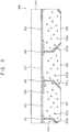
- FIG. 3 is a cross-sectional view illustrating a color conversion panel according to an embodiment.
- FIG. 3 may illustrate an example of the color conversion panel 200 in FIG. 2 .
- a color conversion panel 300 may include a substrate 310, a first color filter 321, a second color filter 322, a third color filter 323, a first light blocking pattern 324, a first color conversion pattern 331, a second color conversion pattern 332, a transmission pattern 333, a first reflective partition wall 341, and a second reflective partition wall 342.
- the substrate 310 may be a transparent insulating substrate.
- the substrate 310 may be formed of glass, quartz, translucent plastic, or the like.
- the substrate 310 maybe a flexible substrate.
- the first color filter 321 may be disposed on the substrate 310.
- the first color filter 321 may be a wavelength-selective optical filter that transmits light of a specific wavelength band and blocks light of another specific wavelength band. In other words, the first color filter 321 may selectively transmit only a partial wavelength band of light incident thereon.
- the first color filter 321 may include a pigment or dye that absorbs light of a specific wavelength band.
- the first color filter 321 may selectively transmit light having a peak wavelength longer than the peak wavelength of the incident light LI provided by the display panel 100, and may block the incident light LI.
- the first color filter 321 may be disposed in the first pixel PX1 in a plan view, may transmit a first light L1 including the peak wavelength of the first color converted by the first color conversion pattern 331, and may absorb or reflect the incident light LI including the peak wavelength of the third color that is not converted by the first color conversion pattern 331.
- the second color filter 322 may be disposed on the substrate 310. In an embodiment, the second color filter 322 may partially overlap the first color filter 321. For example, the second color filter 322 may be disposed on the substrate 310 while covering a portion of the first color filter 321.
- the second color filter 322 may be a wavelength-selective optical filter that transmits light of a specific wavelength band and blocks light of another specific wavelength band. In other words, the second color filter 322 may selectively transmit only a partial wavelength band of light incident thereon.
- the second color filter 322 may include a pigment or dye that absorbs light of a specific wavelength band.
- the second color filter 322 may selectively transmit light having a peak wavelength longer than the peak wavelength of the incident light LI provided by the display panel 100, and may block the incident light LI.
- the second color filter 322 may be disposed in the second pixel PX2 in a plan view, may transmit a second light L2 including the peak wavelength of the second color converted by the second color conversion pattern 332, and may absorb or reflect the incident light LI including the peak wavelength of the third color that is not converted by the second color conversion pattern 332.
- the third color filter 323 may be disposed on the substrate 310. In an embodiment, the third color filter 323 may partially overlap the first color filter 321 and the second color filter 322. The third color filter 323 may be disposed between the first color filter 321 and the second color filter 322 spaced apart from each other. For example, the first color filter 321 may be disposed on the substrate 310 while covering a portion of the third color filter 323, and the second color filter 322 may be disposed on the substrate 310 while covering another portion of the third color filter 323.
- the third color filter 323 may be a wavelength-selective optical filter that transmits light of a specific wavelength band and blocks light of another specific wavelength band. In other words, the third color filter 323 may selectively transmit only a partial wavelength band of light incident thereon.
- the third color filter 323 may include a pigment or dye that absorbs light of a specific wavelength band.
- the third color filter 323 may selectively transmit the incident light LI provided by the display panel 100.
- the third color filter 323 may be disposed in the third pixel PX3 in a plan view, may transmit a third light L3 including the peak wavelength of the third color corresponding to the incident light LI transmitted by the transmission pattern 333.
- the first light blocking pattern 324 may be disposed on the substrate 310. In an embodiment, the first light blocking pattern 324 may partially overlap the first color filter 321 and the second color filter 322. The first light blocking pattern 324 may be disposed between the first color filter 321 and the second color filter 322 that partially overlap each other. For example, the first color filter 321 may be disposed on the substrate 310 while covering a portion of the first light blocking pattern 324, and the second color filter 322 may be disposed on the substrate 310 while covering another portion of the first light blocking pattern 324.
- the first light blocking pattern 324 may be a wavelength-selective optical filter that transmits light of a specific wavelength band and blocks light of another specific wavelength band. In other words, the first light blocking pattern 324 may selectively transmit only a partial wavelength band of light incident thereon.
- the first light blocking pattern 324 may include substantially the same material as the third color filter 323.
- the first color conversion pattern 331 may be disposed on the substrate 310 with the first color filter 321 interposed therebetween. In other words, the first color filter 321 may be disposed between the substrate 310 and the first color conversion pattern 331.
- the first color conversion pattern 331 may convert incident light into transmitted light having a color different from a color of the incident light. In other words, the light transmitted through the first color conversion pattern 331 may be converted into light of a predetermined specific wavelength band.
- the first color conversion pattern 331 may include a first color conversion material 331p, which is a material that converts a peak wavelength of the incident light into a predetermined specific peak wavelength.
- the first color conversion pattern 331 may convert a color of the incident light LI provided by the display panel 100.
- the first color conversion pattern 331 may convert the incident light LI including the peak wavelength of the third color into the first light L1 including the peak wavelength of the first color.
- the incident light LI provided by the display panel 100 may be converted into the first light L1 by the first color conversion pattern 331, and the first light L1 may be emitted to above the color conversion panel 300 through the first color filter 321. Accordingly, the first pixel PX1 may display the first color.
- the second color conversion pattern 332 may be disposed on the substrate 310 with the second color filter 322 interposed therebetween. In other words, the second color filter 322 may be disposed between the substrate 310 and the second color conversion pattern 332.
- the second color conversion pattern 332 may convert incident light into transmitted light having a color different from a color of the incident light. In other words, the light transmitted through the second color conversion pattern 332 may be converted into light of a predetermined specific wavelength band.
- the second color conversion pattern 332 may include a second color conversion material 332p, which is a material that converts a peak wavelength of the incident light into a predetermined specific peak wavelength.
- the second color conversion pattern 332 may convert a color of the incident light LI provided by the display panel 100.
- the second color conversion pattern 332 may convert the incident light LI including the peak wavelength of the third color into the second light L2 including the peak wavelength of the second color.
- the incident light LI provided by the display panel 100 may be converted into the second light L2 by the second color conversion pattern 332, and the second light L2 may be emitted to above the color conversion panel 300 through the second color filter 322. Accordingly, the second pixel PX2 may display the second color.
- a height of the second color conversion pattern 332 from the substrate 310 may be substantially equal to a height of the first color conversion pattern 331 from the substrate 310.
- the height of the first color conversion pattern 331 may be a distance from the substrate 310 to a lower surface of the first color conversion pattern 331, and the height of the second color conversion pattern 332 may be a distance from the substrate 310 to a lower surface of the second color conversion pattern 332.
- the first color conversion material 331p may be a material that emits light having a peak wavelength of the first color.
- the size of the first color conversion material 331p may be about 55 ⁇ to about 65 ⁇ , however, the size of the first color conversion material 331p is not limited thereto.
- the second color conversion material 332p may be a material that emits light having a peak wavelength of the second color.
- the size of the second color conversion material 332p may be about 40 ⁇ to about 50 ⁇ , however, the size of the second color conversion material 332p is not limited thereto.
- each of the first color conversion pattern 331 and the second color conversion pattern 332 may include at least one of a quantum dot and a phosphor.
- each of the first color conversion material 331p and the second color conversion material 332p maybe at least one of the quantum dot and the phosphor.
- the quantum dot may emit a specific color when electrons transit from a conduction band to a valence band.
- the quantum dot may have a core-shell structure.
- the core may be a semiconductor nanocrystalline material.
- the core may include silicon-based nanocrystals, II-VI-based compound nanocrystals, III-V-based compound nanocrystals, or the like, however, the material of the core is not limited thereto.
- the quantum dot may include a core containing cadmium selenide (CdSe), cadmium telluride (CdTe), cadmium sulfide (CdS), or indium phosphide (InP) and a shell containing zinc sulfide (ZnS).
- the second color conversion pattern 332 may partially overlap the first color conversion pattern 331.
- a portion of the second color conversion pattern 332 may overlap a portion of the first color conversion pattern 331.
- the portion of the second color conversion pattern 332 may be positioned under the portion of the first color conversion pattern 331.
- the volume of the first color conversion pattern 331 and the volume of the second color conversion pattern 332 may increase. Accordingly, color conversion efficiency of the first color conversion pattern 331 and color conversion efficiency of the second color conversion pattern 332 may increase.
- the transmission pattern 333 may be disposed on the substrate 310 with the third color filter 323 interposed therebetween. In other words, the third color filter 323 may be disposed between the substrate 310 and the transmission pattern 333.
- the transmission pattern 333 may transmit incident light while maintaining the color of the incident light. In other words, the light transmitted through the transmission pattern 333 may not be converted.
- the transmission pattern 333 may include a transmissive material 333p.
- the transmission pattern 333 may transmit the incident light LI provided by the display panel 100.
- the transmission pattern 333 may transmit the incident light LI including the peak wavelength of the third color, and may emit the third light L3 including the peak wavelength of the third color.
- the incident light LI provided by the display panel 100 may be transmitted through the transmission pattern 333, and the third light L3 corresponding to the incident light LI may be emitted to above the color conversion panel 300 through the third color filter 323. Accordingly, the third pixel PX3 may display the third color.
- a height of the transmission pattern 333 from the substrate 310 maybe substantially equal to the height of the first color conversion pattern 331 from the substrate 310 and the height of the second color conversion pattern 332 from the substrate 310.
- the height of the transmission pattern 333 may be a distance from the substrate 310 to a lower surface of the transmission pattern 333.
- the transmissive material 333p may be a light scattering material that induces scattering of light passing through the transmission pattern 333.
- the transmissive material 333p is not particularly limited as long as it is a material capable of scattering or reflecting light, and may be, for example, a metal oxide, an organic material, or the like.
- the metal oxide may include titanium oxide, zirconium oxide, aluminum oxide, indium oxide, zinc oxide, tin oxide or the like
- the organic material may include acrylic resin, urethane resin or the like.
- the transmission pattern 333 may partially overlap the first color conversion pattern 331 and the second color conversion pattern 332.
- a portion of the transmission pattern 333 may overlap a portion of the first color conversion pattern 331, and another portion of the transmission pattern 333 may overlap a portion of the second color conversion pattern 332.
- the portion of the first color conversion pattern 331 may be positioned under the portion of the transmission pattern 333
- the portion of the second color conversion pattern 332 may be positioned under the another portion of the transmission pattern 333.
- the transmission pattern 333 partially overlaps the first color conversion pattern 331 and the second color conversion pattern 332
- the volume of the first color conversion pattern 331, the volume of the second color conversion pattern 332, and the volume of the transmission pattern 333 may increase. Accordingly, color conversion efficiency of the first color conversion pattern 331 and color conversion efficiency of the second color conversion pattern 332 may increase.
- the first reflective partition wall 341 may be disposed between the first color conversion pattern 331 and the second color conversion pattern 332.
- the first reflective partition wall 341 may be disposed on the second color filter 322 between the first color conversion pattern 331 and the second color conversion pattern 332 adjacent to each other.
- the first reflective partition wall 341 may reflect light emitted to a side 331s of the first color conversion pattern 331 and a side of the second color conversion pattern 332 to emit the light toward the substrate 310.
- the first reflective partition wall 341 is disposed between the first color conversion pattern 331 and the second color conversion pattern 332 partially overlapping each other, color mixture defects due to the partial overlap between the first color conversion pattern 331 and the second color conversion pattern 332 may be prevented.
- the first reflective partition wall 341 may cover the side 331s of the first color conversion pattern 331.
- the first reflective partition wall 341 may entirely cover the side 331s of the first color conversion pattern 331 positioned between the first color conversion pattern 331 and the second color conversion pattern 332.
- the first reflective partition wall 341 may be formed along a profile of the side 331s of the first color conversion pattern 331 positioned between the first color conversion pattern 331 and the second color conversion pattern 332.
- a height of the first reflective partition wall 341 from the substrate 310 may be substantially equal to the height of the first color conversion pattern 331 from the substrate 310.
- the height of the first reflective partition wall 341 may be a distance from the substrate 310 to a lower surface of the first reflective partition wall 341.
- the second color conversion pattern 332 may not contact the first color conversion pattern 331. Accordingly, light emission efficiency of the first color conversion pattern 331 and the second color conversion pattern 332 may increase.
- the second reflective partition wall 342 may be disposed between the first color conversion pattern 331 and the transmission pattern 333 and between the second color conversion pattern 332 and the transmission pattern 333.
- the second reflective partition wall 342 may be disposed on the first color filter 321 between the first color conversion pattern 331 and the transmission pattern 333 adjacent to each other and on the second color filter 322 between the second color conversion pattern 332 and the transmission pattern 333 adjacent to each other.
- the second reflective partition wall 342 may reflect light emitted to the side 331s of the first color conversion pattern 331, a side of the second color conversion pattern 332, and a side 333s of the transmission pattern 333 to emit the light toward the substrate 310.
- the second reflective partition wall 342 is disposed between the first color conversion pattern 331 and the transmission pattern 333 partially overlapping each other and between the second color conversion pattern 332 and the transmission pattern 333 partially overlapping each other, color mixture defects due to the partial overlap between the first color conversion pattern 331 and the transmission pattern 333 and color mixture defects due to the partial overlap between the second color conversion pattern 332 and the transmission pattern 333 may be prevented.
- the second reflective partition wall 342 may cover the side 333s of the transmission pattern 333.
- the second reflective partition wall 342 may entirely cover the side 333s of the transmission pattern 333 positioned between the transmission pattern 333 and the first color conversion pattern 331 and between the transmission pattern 333 and the second color conversion pattern 332.
- the second reflective partition wall 342 may be formed along a profile of the side 333s of the transmission pattern 333 positioned between the transmission pattern 333 and the first color conversion pattern 331 and between the transmission pattern 333 and the second color conversion pattern 332.
- a height of the second reflective partition wall 342 from the substrate 310 may be substantially equal to the height of the transmission pattern 333 from the substrate 310.
- the height of the second reflective partition wall 342 may be a distance from the substrate 310 to a lower surface of the second reflective partition wall 342. As the second reflective partition wall 342 entirely covers the side 333s of the transmission pattern 333, the transmission pattern 333 may not contact the first color conversion pattern 331 and the second color conversion pattern 332. Accordingly, light emission efficiency of the first color conversion pattern 331, the second color conversion pattern 332, and the transmission pattern 333 may increase.
- the first reflective partition wall 341 and the second reflective partition wall 342 may include a material capable of reflecting light, for example, a material having a reflectance of about 50% or more.
- the first reflective partition wall 341 and the second reflective partition wall 342 may have a single-layer structure including aluminum (Al), etc. or a multilayer structure including indium tin oxide (ITO)-silver (Ag)-ITO, titanium (Ti)-Al-Ti, Al-manganese tin oxide (MTO), etc., however, materials of the first and second reflective partition walls 341 and 342 are not limited thereto.
- the first reflective partition wall 341 and the second reflective partition wall 342 may include substantially the same material.
- color conversion efficiency of the color conversion panel 300 may be improved.
- first reflective partition wall 341 is disposed between the first color conversion pattern 331 and the second color conversion pattern 332 which partially overlap each other, color mixture of the color conversion panel 300 may be prevented. Accordingly, a high-resolution display device in which color conversion efficiency is improved and color mixture is prevented may be provided.
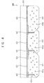
- FIG. 4 is a cross-sectional view illustrating a color conversion panel according to an embodiment.
- a color conversion panel 400 may include a substrate 410, a first color filter 421, a second color filter 422, a third color filter 423, a first light blocking pattern 424, a first color conversion pattern 431, a second color conversion pattern 432, a transmission pattern 433, a first reflective partition wall 441, and a second reflective partition wall 442. Descriptions on components of the color conversion panel 400 described with reference to FIG. 4 , which are substantially the same as or similar to those of the color conversion panel 300 described with reference to FIG. 3 , will not be repeated.
- a height of the first reflective partition wall 441 from the substrate 410 may be less than a height of the first color conversion pattern 431 from the substrate 410.
- the first reflective partition wall 441 may cover a portion of a side of the first color conversion pattern 431 close to the substrate 410, and may not cover another portion of the side of the first color conversion pattern 431 far from the substrate 410. Accordingly, the second color conversion pattern 432 may contact the first color conversion pattern 431 under the first reflective partition wall 441.
- the second color conversion pattern 432 may cover the first reflective partition wall 441, and the first reflective partition wall 441 may not be exposed to the outside by the second color conversion pattern 432. Accordingly, reflection of incident light by the first reflective partition wall 441 exposed to the outside may be prevented.
- a height of the second reflective partition wall 442 from the substrate 410 may be less than a height of the transmission pattern 433 from the substrate 410.
- the second reflective partition wall 442 may cover a portion of a side of the transmission pattern 433 close to the substrate 410, and may not cover another portion of the side of the transmission pattern 433 far from the substrate 410. Accordingly, the first color conversion pattern 431 and the second color conversion pattern 432 may contact the transmission pattern 433 under the second reflective partition wall 442.
- the first color conversion pattern 431 and the second color conversion pattern 432 may cover the second reflective partition wall 442, and the second reflective partition wall 442 may not be exposed to the outside by the first color conversion pattern 431 and the second color conversion pattern 432. Accordingly, reflection of incident light by the second reflective partition wall 442 exposed to the outside may be prevented.
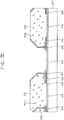
- FIG. 5 is a cross-sectional view illustrating a color conversion panel according to an embodiment.
- a color conversion panel 500 may include a substrate 510, a first color filter 521, a second color filter 522, a third color filter 523, a first light blocking pattern 524, a first color conversion pattern 531, a second color conversion pattern 532, a transmission pattern 533, a first reflective partition wall 541, a second reflective partition wall 542, and a second light blocking pattern 550. Descriptions on components of the color conversion panel 500 described with reference to FIG. 5 , which are substantially the same as or similar to those of the color conversion panel 300 described with reference to FIG. 3 will not be repeated.
- the second light blocking pattern 550 partially overlapping the first color conversion pattern 531, the second color conversion pattern 532, and the transmission pattern 533 may be disposed between the first color conversion pattern 531, the second color conversion pattern 532, and the transmission pattern 533.
- the second light blocking pattern 550 may be disposed between the substrate 510 and the first color conversion pattern 531, between the substrate 510 and the second color conversion pattern 532, and between the substrate 510 and the transmission pattern 533.
- a portion of the second light blocking pattern 550 positioned between the first color conversion pattern 531 and the second color conversion pattern 532 may be disposed on the first light blocking pattern 524, and another portion of the second light blocking pattern 550 positioned between the first color conversion pattern 531 and the transmission pattern 533 and between the second color conversion pattern 532 and the transmission pattern 533 may be disposed on the third color filter 523.
- the second light blocking pattern 550 may partition areas in which the first color conversion pattern 531, the second color conversion pattern 532, and the transmission pattern 533 are disposed.
- the second light blocking pattern 550 may block light transmission.
- the second light blocking pattern 550 may include a material capable of blocking transmission of light, for example, an organic material including a colorant such as a black pigment, a black dye, etc., however, the material of the second light blocking pattern 550 is limited thereto.
- the colorant may include inorganic pigments such as carbon black, titanium black, lignin black, perylene black, cyanine black, etc., complex oxide pigments such as iron/manganese, etc., or a combination thereof.
- a width of the second light blocking pattern 550 may be greater than a width of a first area OA1 in which the first color conversion pattern 531 and the second color conversion pattern 532 overlap, a width of a second area OA2 in which the first color conversion pattern 531 and the transmission pattern 533 overlap, and a width of a third area OA3 in which the second color conversion pattern 532 and the transmission pattern 533 overlap.
- each of the width of the first area OA1, the width of the second area OA2, and the width of the third area OA3 may be about 5 ⁇ m to about 20 ⁇ m, and the width of the second light blocking pattern 550 may be greater than about 20 ⁇ m.
- the second light blocking pattern 550 may prevent color mixture defects between the first color conversion patterns 531, the second color conversion patterns 532, and the transmission patterns 533 adjacent to each other.
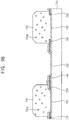
- FIG. 6 is a cross-sectional view illustrating a color conversion panel according to an embodiment.
- a color conversion panel 600 may include a substrate 610, a first color filter 621, a second color filter 622, a third color filter 623, a first light blocking pattern 624, a first color conversion pattern 631, a second color conversion pattern 632, a transmission pattern 633, a first reflective partition wall 641, a second reflective partition wall 642, a second light blocking pattern 650, and a third light blocking pattern 660.
- Descriptions on components of the color conversion panel 600 described with reference to FIG. 6 which are substantially the same as or similar to those of the color conversion panel 500 described with reference to FIG. 5 , will not be repeated.
- the third light blocking pattern 660 partially overlapping the first color conversion pattern 631, the second color conversion pattern 632, and the transmission pattern 633 may be disposed between the first color conversion pattern 631, the second color conversion pattern 632, and the transmission pattern 633.
- the third light blocking pattern 660 may be disposed on the first color conversion pattern 631, the second color conversion pattern 632, and the transmission pattern 633.
- a portion of the third light blocking pattern 660 positioned between the first color conversion pattern 631 and the second color conversion pattern 632 may cover the first reflective partition wall 641 that is not covered by the second color conversion pattern 632
- another portion of the third light blocking pattern 660 positioned between the first color conversion pattern 631 and the transmission pattern 633 and between the second color conversion pattern 632 and the transmission pattern 633 may cover the second reflective partition wall 642 that is not covered by the first color conversion pattern 631 and the second color conversion pattern 632.
- the third light blocking pattern 660 may partition areas in which the first color conversion pattern 631, the second color conversion pattern 632, and the transmission pattern 633 are disposed.
- the third light blocking pattern 660 may block light transmission.
- the third light blocking pattern 660 may include a material capable of blocking transmission of light, for example, an organic material including a colorant such as a black pigment, a black dye, etc., however, the material of the third light blocking pattern 660 is limited thereto.
- the third light blocking pattern 660 may include a material substantially the same as the material of the second light blocking pattern 650.
- a width of the third light blocking pattern 660 may be greater than a width of the first area OA1 in which the first color conversion pattern 631 and the second color conversion pattern 632 overlap, a width of the second area OA2 in which the first color conversion pattern 631 and the transmission pattern 633 overlap, and a width of the third area OA3 in which the second color conversion pattern 632 and the transmission pattern 633 overlap.
- each of the width of the first area OA1, the width of the second area OA2, and the width of the third area OA3 may be about 5 ⁇ m to about 20 ⁇ m, and the width of the third light blocking pattern 660 may be greater than about 20 ⁇ m.
- the third light blocking pattern 660 may prevent color mixture defects between the first color conversion pattern 631, the second color conversion pattern 632, and the transmission pattern 633 adjacent to each other.
- FIGS. 7A , 7B , 7C , 7D , and 7E are cross-sectional views illustrating a method of manufacturing a color conversion panel according to an embodiment.
- FIGS. 7A , 7B , 7C , 7D , and 7E may illustrate a method of manufacturing the color conversion panel 600 in FIG. 6 .
- the transmission pattern 633 may be formed on the substrate 610.
- the third color filter 623 and the first light blocking pattern 624 may be formed on the substrate 610 to be spaced apart from each other.
- the third color filter 623 and the first light blocking pattern 624 may be substantially simultaneously formed of substantially the same material.
- the second light blocking pattern 650 may be formed on the third color filter 623 and the first light blocking pattern 624.
- the first color filter 621 may be formed between the third color filter 623 and the first light blocking pattern 624 on the substrate 610 not covered by the third color filter 623.
- the second color filter 622 may be formed between the third color filter 623 and the first light blocking pattern 624 on the substrate 610 not covered by the first color filter 621 and the third color filter 623.
- the transmission pattern 633 may be formed on the third color filter 623.
- the transmission pattern 633 may be formed to partially overlap the first color filter 621 and the second color filter 622.
- the transmission pattern 633 may be formed by a photolithography method.
- a photosensitive resin including the transmissive material 633p may be applied on the substrate 610, and may be patterned to form the transmission pattern 633.
- the transmission pattern 633 may be formed by an inkjet method.
- an ink composition including the transmissive material 633p may be discharged on the third color filter 623, and may be dried and cured to form the transmission pattern 633.
- the method of forming the transmission pattern 633 is not limited to the photolithography method and the inkjet method described above, and the transmission pattern 633 may be formed by various methods such as a dispensing method, a printing method, a nanoimprinting method, a slit coating method, or the like.
- the second reflective partition wall 642 covering the side of the transmission pattern 633 may be formed on the substrate 610 on which the transmission pattern 633 is formed.
- the second reflective partition wall 642 may be formed on the first color filter 621 and the second color filter 622 to cover the side of the transmission pattern 633.
- the second reflective partition wall 642 may be formed by chemical vapor deposition, sputtering, or the like.
- a conductive material may be deposited on the substrate 610 on which the transmission pattern 633 is formed, and then may be patterned using a photolithography method to form the second reflective partition wall 642.
- the second reflective partition wall 642 may be formed along a profile of the side of the transmission pattern 633.
- the first color conversion pattern 631 partially overlapping the transmission pattern 633 may be formed on the substrate 610 on which the second reflective partition wall 642 is formed.
- the first color conversion pattern 631 may be formed to partially overlap the second color filter 622 and the third color filter 623.
- the first color conversion pattern 631 may be formed by a photolithography method.
- a photosensitive resin including the first color conversion material 631p may be applied on the substrate 610 on which the second reflective partition wall 642 is formed, and may be patterned to form the first color conversion pattern 631.
- the first color conversion material 631p may be injected to form the first color conversion pattern 631.
- the first color conversion pattern 631 may be formed by an inkjet method.
- an ink composition including the first color conversion material 631p may be discharged on the first color filter 621, and may be dried and cured to form the first color conversion pattern 631.
- the method of forming the first color conversion pattern 631 is not limited to the photolithography method and the inkjet method described above, and the first color conversion pattern 631 may be formed by various methods such as a dispensing method, a printing method, a nanoimprinting method, a slit coating method, or the like.
- the first reflective partition wall 641 covering the side of the first color conversion pattern 631 may be formed on the substrate 610 on which the first color conversion pattern 631 is formed.
- the first reflective partition wall 641 may be formed on the second color filter 622 to cover the side of the first color conversion pattern 631.
- the first reflective partition wall 641 may be formed by chemical vapor deposition, sputtering, or the like.
- a conductive material may be deposited on the substrate 610 on which the first color conversion pattern 631 is formed, and may be patterned using a photolithography method to form the first reflective partition wall 641.
- the first reflective partition wall 641 may be formed along a profile of the side of the first color conversion pattern 631.
- the second color conversion pattern 632 partially overlapping the transmission pattern 633 and the first color conversion pattern 631 may be formed on the substrate 610 on which the first reflective partition wall 641 is formed.
- the second color conversion pattern 632 may be formed by a photolithography method.
- a photosensitive resin including the second color conversion material 632p may be applied on the substrate 610 on which the first reflective partition wall 641 is formed, and may be patterned to form the second color conversion pattern 632.
- the second color conversion material 632p may be injected to form the second color conversion pattern 632.
- the second color conversion pattern 632 may be formed by an inkjet method.
- an ink composition including the second color conversion material 632p may be discharged on the second color filter 622, and may be dried and cured to form the second color conversion pattern 632.
- the method of forming the second color conversion pattern 632 is not limited to the photolithography method and the inkjet method described above, and the second color conversion pattern 632 may be formed by various methods such as a dispensing method, a printing method, a nanoimprinting method, a slit coating method, or the like.
- the third light blocking pattern 660 may be formed on the first color conversion pattern 631, the second color conversion pattern 632, and the transmission pattern 633 between the first color conversion pattern 631, the second color conversion pattern 632, and the transmission pattern 633.
- FIG. 8 is a cross-sectional view illustrating a color conversion panel according to an embodiment.
- a color conversion panel 700 may include a substrate 710, a first color filter 721, a second color filter 722, a third color filter 723, a first light blocking pattern 724, a first color conversion pattern 731, a second color conversion pattern 732, a transmission pattern 733, a first reflective partition wall 741, a second reflective partition wall 742, a third reflective partition wall 743, a second light blocking pattern 750, and a third light blocking pattern 760. Descriptions on components of the color conversion panel 700 described with reference to FIG. 8 , which are substantially the same as or similar to those of the color conversion panel 600 described with reference to FIG. 6 , will not be repeated.
- the second color conversion pattern 732 may be spaced apart from the first color conversion pattern 731. In other words, the second color conversion pattern 732 may not overlap the first color conversion pattern 731.
- a width of the first color conversion pattern 731 may be less than a width of the first color filter 721
- a width of the second color conversion pattern 732 may be less than a width of the second color filter 722 .
- the transmission pattern 733 may be spaced apart from the first color conversion pattern 731 and the second color conversion pattern 732. In other words, the transmission pattern 733 may not overlap the first color conversion pattern 731 and the second color conversion pattern 732. For example, a width of the transmission pattern 733 may be less than a width of the third color filter 723.
- the first reflective partition wall 741 may be disposed on a side 731s of the first color conversion pattern 731 to cover the side 731s of the first color conversion pattern 731.
- the first reflective partition wall 741 may be disposed on the first color filter 721 while covering the side 731s of the first color conversion pattern 731.
- the first reflective partition wall 741 may reflect light emitted to the side 731s of the first color conversion pattern 731, and may emit the light toward the substrate 710. Accordingly, light emission efficiency of the first color conversion pattern 731 may increase.
- the first reflective partition wall 741 may entirely cover the side 731s of the first color conversion pattern 731.
- the first reflective partition wall 741 may be formed along a profile of the side 731s of the first color conversion pattern 731.
- a height of the first reflective partition wall 741 from the substrate 710 may be substantially equal to a height of the first color conversion pattern 731 from the substrate 710.
- the height of the first color conversion pattern 731 may be a distance from the substrate 710 to a lower surface of the first color conversion pattern 731
- the height of the first reflective partition wall 741 may be a distance from the substrate 710 to a lower surface of the first reflective partition wall 741.
- the second reflective partition wall 742 may be disposed on a side 732s of the second color conversion pattern 732 to cover the side 732s of the second color conversion pattern 732.
- the second reflective partition wall 742 may be disposed on the second color filter 722 while covering the side 732s of the second color conversion pattern 732.
- the second reflective partition wall 742 may reflect light emitted to the side 732s of the second color conversion pattern 732, and may emit the light toward the substrate 710. Accordingly, light emission efficiency of the second color conversion pattern 732 may increase.
- the second reflective partition wall 742 may entirely cover the side 732s of the second color conversion pattern 732.
- the second reflective partition wall 742 may be formed along a profile of the side 732s of the second color conversion pattern 732.
- a height of the second reflective partition wall 742 from the substrate 710 may be substantially equal to a height of the second color conversion pattern 732 from the substrate 710.
- the height of the second color conversion pattern 732 may be a distance from the substrate 710 to a lower surface of the second color conversion pattern 732
- the height of the second reflective partition wall 742 may be a distance from the substrate 710 to a lower surface of the second reflective partition wall 742.
- the second reflective partition wall 742 may be spaced apart from the first reflective partition wall 741. In other words, a gap may be formed between the first reflective partition wall 741 and the second reflective partition wall 742.
- the third reflective partition wall 743 may be disposed on a side 733s of the transmission pattern 733 to cover the side 733s of the transmission pattern 733.
- the third reflective partition wall 743 may be disposed on the second light blocking pattern 750 while covering the side 733s of the transmission pattern 733.
- the third reflective partition wall 743 may reflect light emitted to the side 733s of the transmission pattern 733, and may emit the light toward the substrate 710. Accordingly, light emission efficiency of the transmission pattern 733 may increase.
- the third reflective partition wall 743 may entirely cover the side 733s of the transmission pattern 733.
- the third reflective partition wall 743 may be formed along a profile of the side 733s of the transmission pattern 733.
- a height of the third reflective partition wall 743 from the substrate 710 may be substantially equal to a height of the transmission pattern 733 from the substrate 710.
- the height of the transmission pattern 733 may be a distance from the substrate 710 to a lower surface of the transmission pattern 733
- the height of the third reflective partition wall 743 may be a distance from the substrate 710 to a lower surface of the third reflective partition wall 743.
- the third reflective partition wall 743 may be spaced apart from the first reflective partition wall 741 and the second reflective partition wall 742. In other words, gaps may be formed between the first reflective partition wall 741 and the third reflective partition wall 743 and between the second reflective partition wall 742 and the third reflective partition wall 743, respectively.
- the third light blocking pattern 760 partially overlapping the first color conversion pattern 731, the second color conversion pattern 732, and the transmission pattern 733 may be disposed between the first color conversion pattern 731, the second color conversion pattern 732, and the transmission pattern 733.
- the third light blocking pattern 760 may be disposed on the first color conversion pattern 731, the second color conversion pattern 732, and the transmission pattern 733 while covering the first reflective partition wall 741, the second reflective partition wall 742, and the third reflective partition wall 743.
- the third light blocking pattern 760 may fill the gaps formed between the first reflective partition wall 741, the second reflective partition wall 742, and the third reflective partition wall 743 spaced apart from each other.
- FIGS. 9A , 9B , 9C , and 9D are cross-sectional views illustrating a method of manufacturing a color conversion panel according to an embodiment.
- FIGS. 9A , 9B , 9C , and 9D may illustrate a method of manufacturing the color conversion panel 700 in FIG. 8 .
- the transmission pattern 733 may be formed on the substrate 710.
- the transmission pattern 733 may be formed on the third color filter 723.
- the transmission pattern 733 may be formed so as not to overlap the first color filter 721 and the second color filter 722 .
- the first color conversion pattern 731 spaced apart from the transmission pattern 733 may be formed on the substrate 710 on which the transmission pattern 733 is formed.
- the first color conversion pattern 731 may be formed on the first color filter 721.
- the first color conversion pattern 731 may be formed so as not to overlap the second color filter 722 and the third color filter 723.
- the second color conversion pattern 732 spaced apart from the transmission pattern 733 and the first color conversion pattern 731 may be formed on the substrate 710 on which the transmission pattern 733 and the first color conversion pattern 731 are formed.
- the second color conversion pattern 732 may be formed on the second color filter 722 .
- the second color conversion pattern 732 may be formed so as not to overlap the first color filter 721.
- the first color conversion pattern 731 is formed after the formation of the transmission pattern 733
- the second color conversion pattern 732 is formed after the formation of the first color conversion pattern 731
- the method of manufacturing the color conversion pattern 700 is not limited thereto.
- the first color conversion pattern 731, the second color conversion pattern 732, and the transmission pattern 733 may be sequentially formed in an arbitrary order, or may be substantially simultaneously formed.
- the first reflective partition wall 741 covering the side of the first color conversion pattern 731, the second reflective partition wall 742 covering the side of the second color conversion pattern 732, and the third reflective partition wall 743 covering the side of the transmission pattern 733 may be formed on the substrate 710 on which the transmission pattern 733, the first color conversion pattern 731, and the second color conversion pattern 732 are formed.
- the first reflective partition wall 741 maybe formed on the first color filter 721 to cover the side of the first color conversion pattern 731
- the second reflective partition wall 742 may be formed on the second color filter 722 to cover the side of the second color conversion pattern 732
- the third reflective partition wall 743 may be formed on the third color filter 723 to cover the side of the transmission pattern 733.
- the first reflective partition wall 741, the second reflective partition wall 742, and the third reflective partition wall 743 may be substantially simultaneously formed of substantially the same material.
- a conductive material may be deposited on the substrate 710 on which the transmission pattern 733, the first color conversion pattern 731, and the second color conversion pattern 732 are formed, and may be patterned using a photolithography method, etc. to form the first reflective partition wall 741, the second reflective partition wall 742, and the third reflective partition wall 743.
- the first reflective partition wall 741, the second reflective partition wall 742, and the third reflective partition wall 743 may be formed along a profile of the side of the first color conversion pattern 731, a profile of the side of the second color conversion pattern 732, and a profile of the side of the transmission pattern 733, respectively. Accordingly, manufacturing cost and manufacturing time for forming the first reflective partition wall 741, the second reflective partition wall 742, and the third reflective partition wall 743 may be reduced.
- FIG. 10 is a cross-sectional view illustrating an example of the display device taken along a line I-I' in FIG. 1 .
- a display device may include a display panel 800, a color conversion panel 900, and a backlight unit 1000.
- the backlight unit 1000 may overlap the display panel 800.
- the backlight unit 1000 may be positioned under the display panel 800.
- the backlight unit 1000 may include a light source generating light and a light guide plate receiving the light and guiding the light toward the display panel 800.
- the backlight unit 1000 may provide incident light LI to the display panel 800.
- the backlight unit 1000 may provide the incident light LI of a third color having a peak wavelength within a range of about 430 nm to about 470 nm to the display panel 800.
- the display panel 800 may include a base substrate 810, a polarizing layer 820, a gate line 830, a gate insulation layer 840, a data line 850, a passivation layer 860, a first electrode 870, a liquid crystal layer 880, and a second electrode 890.
- the display panel 800 may control the incident light LI provided from the backlight unit 1000, and may provide the incident light LI to the color conversion panel 900.
- the polarizing layer 820 may be disposed between the backlight unit 1000 and the base substrate 810.
- the polarizing layer 820 may be a coated polarizing layer, a wire grid polarizer, or the like.
- a gate electrode and the gate line 830 may be disposed on the base substrate 810.
- the gate line 830 may transmit a gate signal, and may extend along one direction.
- the gate insulation layer 840 including silicon nitride, silicon oxide, or the like may be disposed on the gate electrode and the gate line 830.
- a semiconductor layer, a source electrode, a drain electrode, and the data line 850 may be disposed on the gate insulation layer 840.
- the semiconductor layer may overlap the gate electrode, the source electrode and the drain electrode may be connected to the semiconductor layer, and the data line 850 may transmit a data signal and extend in a direction crossing the gate line 830.
- the gate electrode, the semiconductor layer, the source electrode, and the drain electrode may form a thin film transistor.
- the passivation layer 860 including an inorganic insulation material such as silicon nitride or silicon oxide and/or an organic insulation material such as polyimide may be disposed on the semiconductor layer, the source electrode, the drain electrode, and the data line 850.
- the first electrode 870 including a conductive material may be disposed on the passivation layer 860.
- the first electrode 870 may be connected to the source electrode or the drain electrode.
- the second electrode 890 including a conductive material may be disposed on the first electrode 870.
- the liquid crystal layer 880 may be disposed between the first electrode 870 and the second electrode 890.
- the liquid crystal layer 880 may include liquid crystal molecules 885.
- the arrangement direction of the liquid crystal molecules 885 may be controlled by an electric field formed between the first electrode 870 and the second electrode 890.
- the liquid crystal layer 880 may control the transmittance of the incident light LI of the third color provided from the backlight unit 1000 based on the electric field formed between the first electrode 870 and the second electrode 890, and may emit the incident light LI upward.
- the color conversion panel 900 may overlap the display panel 800.
- the color conversion panel 900 may be positioned above the display panel 800.
- the color conversion panel 900 may include a substrate 910, a first color filter 921, a second color filter 922, a third color filter 923, a first color conversion pattern 931, a second color conversion pattern 932, a transmission pattern 933, a first reflective partition wall 941, and a second reflective partition wall 942.
- the color conversion panel 900 may receive the incident light LI provided from the backlight unit 1000 and controlled by the display panel 800, and may emit first light Li, second light L2, and third light L3 upward.
- the display device may be applied to a display device included in a computer, a notebook, a mobile phone, a smartphone, a smart pad, a PMP, a PDA, an MP3 player, or the like.
Landscapes
- Physics & Mathematics (AREA)
- Nonlinear Science (AREA)
- Mathematical Physics (AREA)
- Chemical & Material Sciences (AREA)
- Crystallography & Structural Chemistry (AREA)
- General Physics & Mathematics (AREA)
- Optics & Photonics (AREA)
- Engineering & Computer Science (AREA)
- Microelectronics & Electronic Packaging (AREA)
- Optical Filters (AREA)
- Devices For Indicating Variable Information By Combining Individual Elements (AREA)
Abstract
Description
- Embodiments relate to a display device. More particularly, embodiments relate to a display device including a color conversion panel.
- With the development of information technology, the market for a display device, which is a connection medium between a user and information, is growing. Accordingly, the use of flat panel display devices such as an organic light emitting display device, a liquid crystal display device, or the like is increasing.
- Recently, a display device including a color conversion panel has been proposed to implement a display device having high light efficiency.
- An object of the present invention is to provide a high resolution display device.
- An object of the present invention is to provide a color conversion panel with improved light efficiency.
- In order to achieve the object of the present invention described above, a display device according to embodiments may include a display panel and a color conversion panel overlapping the display panel. The color conversion panel may include a substrate, a first color conversion pattern disposed on the substrate, a second color conversion pattern disposed on the substrate and partially overlapping the first color conversion pattern, a first reflective partition wall disposed between the first color conversion pattern and the second color conversion pattern, a first color filter disposed between the substrate and the first color conversion pattern, and a second color filter disposed between the substrate and the second color conversion pattern.
- In an embodiment, the first reflective partition wall may cover a side of the first color conversion pattern.
- In an embodiment, the second color conversion pattern may not contact the first color conversion pattern.
- In an embodiment, the second color conversion pattern may contact the first color conversion pattern under the first reflective partition wall.
- In an embodiment, the color conversion panel may further include a light blocking pattern partially overlapping the first color conversion pattern and the second color conversion pattern between the first color conversion pattern and the second color conversion pattern.
- In an embodiment, the light blocking pattern may be disposed between the substrate and the first color conversion pattern and between the substrate and the second color conversion pattern.
- In an embodiment, the light blocking pattern may be disposed on the first color conversion pattern and the second color conversion pattern.
- In an embodiment, a width of the light blocking pattern may be greater than a width of an area in which the first color conversion pattern overlaps the second color conversion pattern.
- In an embodiment, the color conversion panel may further include a transmission pattern disposed on the substrate and partially overlapping the first color conversion pattern and the second color conversion pattern.
- In an embodiment, the color conversion panel may further include a second reflective partition wall disposed between the first color conversion pattern and the transmission pattern and between the second color conversion pattern and the transmission pattern.
- In an embodiment, the second reflective partition wall may cover a side of the transmission pattern.
- In an embodiment, the transmission pattern may not contact the first color conversion pattern and the second color conversion pattern.
- In an embodiment, the transmission pattern may contact the first color conversion pattern and the second color conversion pattern under the second reflective partition wall.
- In an embodiment, the display panel may be configured to emit a first color light to the color conversion panel, and the first color conversion pattern may be configured to convert the first color light into a second color light. The second color conversion pattern may be configured to convert the first color light into a third color light, and the transmission pattern may be configured to transmit the first color light.
- In an embodiment, each of the first color conversion pattern and the second color conversion pattern may include at least one of a quantum dot and a phosphor.
- In order to achieve the object of the present invention described above, a color conversion panel according to embodiments may include a substrate, a first color conversion pattern disposed on the substrate and configured to convert an incident light into a first color light, a second color conversion pattern disposed on the substrate, partially overlapping the first color conversion pattern, and configured to convert the incident light into a second color light, a first reflective partition wall disposed between the first color conversion pattern and the second color conversion pattern, a first color filter disposed between the substrate and the first color conversion pattern and configured to block the incident light that is not converted by the first color conversion pattern, and a second color filter disposed between the substrate and the second color conversion pattern and configured to block the incident light that is not converted by the second color conversion pattern.
- In an embodiment, the color conversion panel may further include a transmission pattern disposed on the substrate, partially overlapping the first color conversion pattern, and configured to transmit the incident light.
- In an embodiment, the color conversion panel may further include a second reflective partition wall disposed between the first color conversion pattern and the transmission pattern.
- In an embodiment, the color conversion panel may further include a light blocking pattern partially overlapping the first color conversion pattern and the second color conversion pattern between the first color conversion pattern and the second color conversion pattern, and partially overlapping the first color conversion pattern and the transmission pattern between the first color conversion pattern and the transmission pattern.
- In an embodiment, the light blocking pattern may be disposed between the substrate and the first color conversion pattern, between the substrate and the second color conversion pattern, and between the substrate and the transmission pattern.
- In an embodiment, the light blocking pattern may be disposed on the first color conversion pattern, the second color conversion pattern, and the transmission pattern.
- In order to achieve the object of the present invention described above, a color conversion panel according to embodiments may include a substrate, a first color conversion pattern disposed on the substrate and configured to convert an incident light into a first color light, a second color conversion pattern disposed on the substrate, spaced apart from the first color conversion pattern, and configured to convert the incident light into a second color light, a first reflective partition wall covering a side of the first color conversion pattern, a second reflective partition wall covering a side of the second color conversion pattern, a first color filter disposed between the substrate and the first color conversion pattern and configured to block the incident light that is not converted by the first color conversion pattern, and a second color filter disposed between the substrate and the second color conversion pattern and configured to block the incident light that is not converted by the second color conversion pattern.
- In an embodiment, the color conversion panel may further include a transmission pattern disposed on the substrate, spaced apart from the first color conversion pattern and the second color conversion pattern, and configured to transmit the incident light.
- In an embodiment, the color conversion panel may further include a third reflective partition wall covering a side of the transmission pattern.
- In an embodiment, the color conversion panel may further include a light blocking pattern partially overlapping the first color conversion pattern and the second color conversion pattern between the first color conversion pattern and the second color conversion pattern, partially overlapping the first color conversion pattern and the transmission pattern between the first color conversion pattern and the transmission pattern, and partially overlapping the second color conversion pattern and the transmission pattern between the second color conversion pattern and the transmission pattern.
- In an embodiment, the light blocking pattern may cover the first reflective partition wall, the second reflective partition wall, and the third reflective partition wall.
- In an embodiment, the second reflective partition wall may be spaced apart from the first reflective partition wall.
- In the color conversion panel of the display device according to the embodiments, the color conversion patterns may partially overlap, and the reflective partition wall may be disposed between the partially overlapping color conversion patterns, so that a high resolution display device in which color conversion efficiency, light efficiency, or the like are improved may be provided.
- In the color conversion panel according to the embodiments, the color conversion patterns may partially overlap, and the reflective partition wall may be disposed between the partially overlapping color conversion patterns, so that color conversion efficiency, light efficiency, or the like of the color conversion panel may be improved, and color mixture or the like may be prevented.
-
- FIG. is a plan view illustrating a display device according to an embodiment.
-
FIG. 2 is a cross-sectional view illustrating an example of the display device taken along a line I-I' inFIG. 1 . -
FIG. 3 is a cross-sectional view illustrating a color conversion panel according to an embodiment. -
FIG. 4 is a cross-sectional view illustrating a color conversion panel according to an embodiment. -
FIG. 5 is a cross-sectional view illustrating a color conversion panel according to an embodiment. -
FIG. 6 is a cross-sectional view illustrating a color conversion panel according to an embodiment. -
FIGS. 7A ,7B ,7C ,7D , and7E are cross-sectional views illustrating a method of manufacturing a color conversion panel according to an embodiment. -
FIG. 8 is a cross-sectional view illustrating a color conversion panel according to an embodiment. -
FIGS. 9A ,9B ,9C , and9D are cross-sectional views illustrating a method of manufacturing a color conversion panel according to an embodiment. -
FIG. 10 is a cross-sectional view illustrating an example of the display device taken along a line I-I' inFIG. 1 . - Hereinafter, display devices and color conversion panels in accordance with embodiments of the present invention will be explained in detail with reference to the accompanying drawings.
-
FIG. 1 is a plan view illustrating a display device according to an embodiment. - Referring to
FIG. 1 , a plurality of pixels arranged in a substantially matrix form in a plan view may be defined in a display device according to an embodiment. A 'pixel' refers to a single area defined by partitioning a display area in a plan view for color display, and one pixel may display one predetermined basic color. In other words, one pixel may be a minimum unit capable of displaying a color independent from other pixels. - The pixels may include a first pixel PX1 displaying a first color, a second pixel PX2 displaying a second color having a peak wavelength shorter than that of the first color, and a third pixel displaying a third color having a peak wavelength shorter than that of the second color. In an embodiment, the first pixel PX1, the second pixel PX2, and the third pixel PX3, which are sequentially arranged in one direction, may form a basic unit, and maybe repeatedly arranged in the direction.
- In an embodiment, the first pixel PX1 may be a pixel that displays a first color (red) having a peak wavelength within a range of about 610 nm to about 650 nm, the second pixel PX2 may be a pixel that displays a second color (green) having a peak wavelength within a range of about 530 nm to 570 nm, and the third pixel (PX3) may be a pixel that displays a third color (blue) having a peak wavelength within a range of about 430 nm to about 470 nm.
-
FIG. 2 is a cross-sectional view illustrating an example of the display device taken along a line I-I' inFIG. 1 . - Referring to
FIGS. 1 and2 , a display device according to an embodiment may include adisplay panel 100 and acolor conversion panel 200. Thedisplay panel 100 may include abase substrate 110, asemiconductor layer 120, agate insulation layer 130, agate electrode 141, agate line 142, aninsulation interlayer 150, asource electrode 161, adrain electrode 162, adata line 163, aplanarization layer 170, afirst electrode 181, apixel defining layer 190, anemission layer 182, and asecond electrode 183. Thedisplay panel 100 may provide incident light LI to thecolor conversion panel 200. - The
semiconductor layer 120 including amorphous silicon, polycrystalline silicon, oxide semiconductor, or the like may be disposed on thebase substrate 110. Thegate insulation layer 130 including silicon nitride, silicon oxide, or the like may be disposed on thesemiconductor layer 120. - The
gate electrode 141 and thegate line 142 each including a conductive material may be disposed on thegate insulation layer 130. Thegate electrode 141 may overlap thesemiconductor layer 120, and thegate line 142 may transmit a gate signal and may extend along one direction. Theinsulation interlayer 150 including silicon nitride, silicon oxide, or the like may be disposed on thegate electrode 141 and thegate line 142. - The
source electrode 161, thedrain electrode 162, and thedata line 163 each including a conductive material may be disposed on theinsulation interlayer 150. Thesource electrode 161 and thedrain electrode 162 may be connected to thesemiconductor layer 120, and thedata line 163 may transmit a data signal and may extend along a direction crossing thegate line 142. Thesemiconductor layer 120, thegate electrode 141, thesource electrode 161, and thedrain electrode 162 may form a thin film transistor. Theplanarization layer 170 including an inorganic insulation material such as silicon nitride or silicon oxide and/or an organic insulating material such as polyimide may be disposed on thesource electrode 161, thedrain electrode 162, and thedata line 163. - The
first electrode 181 including a conductive material may be disposed on theplanarization layer 170. Thefirst electrode 181 may be connected to thesource electrode 161 or thedrain electrode 162. Thepixel defining layer 190 including an opening that exposes a portion of thefirst electrode 181 may be disposed on theplanarization layer 170. - The
emission layer 182 may be disposed on thefirst electrode 181. Theemission layer 182 may include a material that emits light of the third color. Thesecond electrode 183 including a conductive material may be disposed on theemission layer 182. Theemission layer 182 may emit the incident light LI of the third color to above thedisplay panel 100 based on an electric field formed between thefirst electrode 181 and thesecond electrode 183. In an embodiment, theemission layer 182 may be formed on thefirst electrode 181 and thepixel defining layer 190, however, the present invention is not limited thereto. In another embodiment, theemission layer 182 may be formed in the opening of thepixel defining layer 190 on thefirst electrode 181. - The
color conversion panel 200 may overlap thedisplay panel 100. Thecolor conversion panel 200 may be positioned above thedisplay panel 100. Thecolor conversion panel 200 may include asubstrate 210, afirst color filter 221, asecond color filter 222, athird color filter 223, a firstcolor conversion pattern 231, a secondcolor conversion pattern 232, atransmission pattern 233, a firstreflective partition wall 241, and a secondreflective partition wall 242. Thecolor conversion panel 200 may receive the incident light LI from thedisplay panel 100, and may emit first light L1, second light L2, and third light L3 upward. -
FIG. 3 is a cross-sectional view illustrating a color conversion panel according to an embodiment. For example,FIG. 3 may illustrate an example of thecolor conversion panel 200 inFIG. 2 . - Referring to
FIGS. 1 ,2 , and3 , acolor conversion panel 300 according to an embodiment may include asubstrate 310, afirst color filter 321, asecond color filter 322, athird color filter 323, a firstlight blocking pattern 324, a firstcolor conversion pattern 331, a secondcolor conversion pattern 332, atransmission pattern 333, a firstreflective partition wall 341, and a secondreflective partition wall 342. - The
substrate 310 may be a transparent insulating substrate. For example, thesubstrate 310 may be formed of glass, quartz, translucent plastic, or the like. In an embodiment, thesubstrate 310 maybe a flexible substrate. - The
first color filter 321 may be disposed on thesubstrate 310. Thefirst color filter 321 may be a wavelength-selective optical filter that transmits light of a specific wavelength band and blocks light of another specific wavelength band. In other words, thefirst color filter 321 may selectively transmit only a partial wavelength band of light incident thereon. For example, thefirst color filter 321 may include a pigment or dye that absorbs light of a specific wavelength band. - In an embodiment, the
first color filter 321 may selectively transmit light having a peak wavelength longer than the peak wavelength of the incident light LI provided by thedisplay panel 100, and may block the incident light LI. For example, thefirst color filter 321 may be disposed in the first pixel PX1 in a plan view, may transmit a first light L1 including the peak wavelength of the first color converted by the firstcolor conversion pattern 331, and may absorb or reflect the incident light LI including the peak wavelength of the third color that is not converted by the firstcolor conversion pattern 331. - The
second color filter 322 may be disposed on thesubstrate 310. In an embodiment, thesecond color filter 322 may partially overlap thefirst color filter 321. For example, thesecond color filter 322 may be disposed on thesubstrate 310 while covering a portion of thefirst color filter 321. Thesecond color filter 322 may be a wavelength-selective optical filter that transmits light of a specific wavelength band and blocks light of another specific wavelength band. In other words, thesecond color filter 322 may selectively transmit only a partial wavelength band of light incident thereon. For example, thesecond color filter 322 may include a pigment or dye that absorbs light of a specific wavelength band. - In an embodiment, the
second color filter 322 may selectively transmit light having a peak wavelength longer than the peak wavelength of the incident light LI provided by thedisplay panel 100, and may block the incident light LI. For example, thesecond color filter 322 may be disposed in the second pixel PX2 in a plan view, may transmit a second light L2 including the peak wavelength of the second color converted by the secondcolor conversion pattern 332, and may absorb or reflect the incident light LI including the peak wavelength of the third color that is not converted by the secondcolor conversion pattern 332. - The
third color filter 323 may be disposed on thesubstrate 310. In an embodiment, thethird color filter 323 may partially overlap thefirst color filter 321 and thesecond color filter 322. Thethird color filter 323 may be disposed between thefirst color filter 321 and thesecond color filter 322 spaced apart from each other. For example, thefirst color filter 321 may be disposed on thesubstrate 310 while covering a portion of thethird color filter 323, and thesecond color filter 322 may be disposed on thesubstrate 310 while covering another portion of thethird color filter 323. Thethird color filter 323 may be a wavelength-selective optical filter that transmits light of a specific wavelength band and blocks light of another specific wavelength band. In other words, thethird color filter 323 may selectively transmit only a partial wavelength band of light incident thereon. For example, thethird color filter 323 may include a pigment or dye that absorbs light of a specific wavelength band. - In an embodiment, the
third color filter 323 may selectively transmit the incident light LI provided by thedisplay panel 100. For example, thethird color filter 323 may be disposed in the third pixel PX3 in a plan view, may transmit a third light L3 including the peak wavelength of the third color corresponding to the incident light LI transmitted by thetransmission pattern 333. - The first
light blocking pattern 324 may be disposed on thesubstrate 310. In an embodiment, the firstlight blocking pattern 324 may partially overlap thefirst color filter 321 and thesecond color filter 322. The firstlight blocking pattern 324 may be disposed between thefirst color filter 321 and thesecond color filter 322 that partially overlap each other. For example, thefirst color filter 321 may be disposed on thesubstrate 310 while covering a portion of the firstlight blocking pattern 324, and thesecond color filter 322 may be disposed on thesubstrate 310 while covering another portion of the firstlight blocking pattern 324. The firstlight blocking pattern 324 may be a wavelength-selective optical filter that transmits light of a specific wavelength band and blocks light of another specific wavelength band. In other words, the firstlight blocking pattern 324 may selectively transmit only a partial wavelength band of light incident thereon. For example, the firstlight blocking pattern 324 may include substantially the same material as thethird color filter 323. - The first
color conversion pattern 331 may be disposed on thesubstrate 310 with thefirst color filter 321 interposed therebetween. In other words, thefirst color filter 321 may be disposed between thesubstrate 310 and the firstcolor conversion pattern 331. The firstcolor conversion pattern 331 may convert incident light into transmitted light having a color different from a color of the incident light. In other words, the light transmitted through the firstcolor conversion pattern 331 may be converted into light of a predetermined specific wavelength band. The firstcolor conversion pattern 331 may include a firstcolor conversion material 331p, which is a material that converts a peak wavelength of the incident light into a predetermined specific peak wavelength. - In an embodiment, the first
color conversion pattern 331 may convert a color of the incident light LI provided by thedisplay panel 100. For example, the firstcolor conversion pattern 331 may convert the incident light LI including the peak wavelength of the third color into the first light L1 including the peak wavelength of the first color. The incident light LI provided by thedisplay panel 100 may be converted into the first light L1 by the firstcolor conversion pattern 331, and the first light L1 may be emitted to above thecolor conversion panel 300 through thefirst color filter 321. Accordingly, the first pixel PX1 may display the first color. - The second
color conversion pattern 332 may be disposed on thesubstrate 310 with thesecond color filter 322 interposed therebetween. In other words, thesecond color filter 322 may be disposed between thesubstrate 310 and the secondcolor conversion pattern 332. The secondcolor conversion pattern 332 may convert incident light into transmitted light having a color different from a color of the incident light. In other words, the light transmitted through the secondcolor conversion pattern 332 may be converted into light of a predetermined specific wavelength band. The secondcolor conversion pattern 332 may include a secondcolor conversion material 332p, which is a material that converts a peak wavelength of the incident light into a predetermined specific peak wavelength. - In an embodiment, the second
color conversion pattern 332 may convert a color of the incident light LI provided by thedisplay panel 100. For example, the secondcolor conversion pattern 332 may convert the incident light LI including the peak wavelength of the third color into the second light L2 including the peak wavelength of the second color. The incident light LI provided by thedisplay panel 100 may be converted into the second light L2 by the secondcolor conversion pattern 332, and the second light L2 may be emitted to above thecolor conversion panel 300 through thesecond color filter 322. Accordingly, the second pixel PX2 may display the second color. - In an embodiment, a height of the second
color conversion pattern 332 from thesubstrate 310 may be substantially equal to a height of the firstcolor conversion pattern 331 from thesubstrate 310. The height of the firstcolor conversion pattern 331 may be a distance from thesubstrate 310 to a lower surface of the firstcolor conversion pattern 331, and the height of the secondcolor conversion pattern 332 may be a distance from thesubstrate 310 to a lower surface of the secondcolor conversion pattern 332. - The first
color conversion material 331p may be a material that emits light having a peak wavelength of the first color. The size of the firstcolor conversion material 331p may be about 55 Å to about 65 Å, however, the size of the firstcolor conversion material 331p is not limited thereto. The secondcolor conversion material 332p may be a material that emits light having a peak wavelength of the second color. The size of the secondcolor conversion material 332p may be about 40 Å to about 50 Å, however, the size of the secondcolor conversion material 332p is not limited thereto. - In an embodiment, each of the first
color conversion pattern 331 and the secondcolor conversion pattern 332 may include at least one of a quantum dot and a phosphor. In other words, each of the firstcolor conversion material 331p and the secondcolor conversion material 332p maybe at least one of the quantum dot and the phosphor. - The quantum dot may emit a specific color when electrons transit from a conduction band to a valence band. The quantum dot may have a core-shell structure. The core may be a semiconductor nanocrystalline material. For example, the core may include silicon-based nanocrystals, II-VI-based compound nanocrystals, III-V-based compound nanocrystals, or the like, however, the material of the core is not limited thereto. For example, the quantum dot may include a core containing cadmium selenide (CdSe), cadmium telluride (CdTe), cadmium sulfide (CdS), or indium phosphide (InP) and a shell containing zinc sulfide (ZnS).
- The second
color conversion pattern 332 may partially overlap the firstcolor conversion pattern 331. A portion of the secondcolor conversion pattern 332 may overlap a portion of the firstcolor conversion pattern 331. For example, the portion of the secondcolor conversion pattern 332 may be positioned under the portion of the firstcolor conversion pattern 331. When the firstcolor conversion pattern 331 and the secondcolor conversion pattern 332 partially overlap, the volume of the firstcolor conversion pattern 331 and the volume of the secondcolor conversion pattern 332 may increase. Accordingly, color conversion efficiency of the firstcolor conversion pattern 331 and color conversion efficiency of the secondcolor conversion pattern 332 may increase. - The
transmission pattern 333 may be disposed on thesubstrate 310 with thethird color filter 323 interposed therebetween. In other words, thethird color filter 323 may be disposed between thesubstrate 310 and thetransmission pattern 333. Thetransmission pattern 333 may transmit incident light while maintaining the color of the incident light. In other words, the light transmitted through thetransmission pattern 333 may not be converted. Thetransmission pattern 333 may include atransmissive material 333p. - In an embodiment, the
transmission pattern 333 may transmit the incident light LI provided by thedisplay panel 100. For example, thetransmission pattern 333 may transmit the incident light LI including the peak wavelength of the third color, and may emit the third light L3 including the peak wavelength of the third color. The incident light LI provided by thedisplay panel 100 may be transmitted through thetransmission pattern 333, and the third light L3 corresponding to the incident light LI may be emitted to above thecolor conversion panel 300 through thethird color filter 323. Accordingly, the third pixel PX3 may display the third color. - In an embodiment, a height of the
transmission pattern 333 from thesubstrate 310 maybe substantially equal to the height of the firstcolor conversion pattern 331 from thesubstrate 310 and the height of the secondcolor conversion pattern 332 from thesubstrate 310. The height of thetransmission pattern 333 may be a distance from thesubstrate 310 to a lower surface of thetransmission pattern 333. - The
transmissive material 333p may be a light scattering material that induces scattering of light passing through thetransmission pattern 333. Thetransmissive material 333p is not particularly limited as long as it is a material capable of scattering or reflecting light, and may be, for example, a metal oxide, an organic material, or the like. For example, the metal oxide may include titanium oxide, zirconium oxide, aluminum oxide, indium oxide, zinc oxide, tin oxide or the like, and the organic material may include acrylic resin, urethane resin or the like. - The
transmission pattern 333 may partially overlap the firstcolor conversion pattern 331 and the secondcolor conversion pattern 332. A portion of thetransmission pattern 333 may overlap a portion of the firstcolor conversion pattern 331, and another portion of thetransmission pattern 333 may overlap a portion of the secondcolor conversion pattern 332. For example, the portion of the firstcolor conversion pattern 331 may be positioned under the portion of thetransmission pattern 333, and the portion of the secondcolor conversion pattern 332 may be positioned under the another portion of thetransmission pattern 333. When thetransmission pattern 333 partially overlaps the firstcolor conversion pattern 331 and the secondcolor conversion pattern 332, the volume of the firstcolor conversion pattern 331, the volume of the secondcolor conversion pattern 332, and the volume of thetransmission pattern 333 may increase. Accordingly, color conversion efficiency of the firstcolor conversion pattern 331 and color conversion efficiency of the secondcolor conversion pattern 332 may increase. - The first
reflective partition wall 341 may be disposed between the firstcolor conversion pattern 331 and the secondcolor conversion pattern 332. For example, the firstreflective partition wall 341 may be disposed on thesecond color filter 322 between the firstcolor conversion pattern 331 and the secondcolor conversion pattern 332 adjacent to each other. The firstreflective partition wall 341 may reflect light emitted to aside 331s of the firstcolor conversion pattern 331 and a side of the secondcolor conversion pattern 332 to emit the light toward thesubstrate 310. As the firstreflective partition wall 341 is disposed between the firstcolor conversion pattern 331 and the secondcolor conversion pattern 332 partially overlapping each other, color mixture defects due to the partial overlap between the firstcolor conversion pattern 331 and the secondcolor conversion pattern 332 may be prevented. - The first
reflective partition wall 341 may cover theside 331s of the firstcolor conversion pattern 331. The firstreflective partition wall 341 may entirely cover theside 331s of the firstcolor conversion pattern 331 positioned between the firstcolor conversion pattern 331 and the secondcolor conversion pattern 332. The firstreflective partition wall 341 may be formed along a profile of theside 331s of the firstcolor conversion pattern 331 positioned between the firstcolor conversion pattern 331 and the secondcolor conversion pattern 332. A height of the firstreflective partition wall 341 from thesubstrate 310 may be substantially equal to the height of the firstcolor conversion pattern 331 from thesubstrate 310. The height of the firstreflective partition wall 341 may be a distance from thesubstrate 310 to a lower surface of the firstreflective partition wall 341. As the firstreflective partition wall 341 entirely covers theside 331s of the firstcolor conversion pattern 331, the secondcolor conversion pattern 332 may not contact the firstcolor conversion pattern 331. Accordingly, light emission efficiency of the firstcolor conversion pattern 331 and the secondcolor conversion pattern 332 may increase. - The second
reflective partition wall 342 may be disposed between the firstcolor conversion pattern 331 and thetransmission pattern 333 and between the secondcolor conversion pattern 332 and thetransmission pattern 333. For example, the secondreflective partition wall 342 may be disposed on thefirst color filter 321 between the firstcolor conversion pattern 331 and thetransmission pattern 333 adjacent to each other and on thesecond color filter 322 between the secondcolor conversion pattern 332 and thetransmission pattern 333 adjacent to each other. The secondreflective partition wall 342 may reflect light emitted to theside 331s of the firstcolor conversion pattern 331, a side of the secondcolor conversion pattern 332, and aside 333s of thetransmission pattern 333 to emit the light toward thesubstrate 310. As the secondreflective partition wall 342 is disposed between the firstcolor conversion pattern 331 and thetransmission pattern 333 partially overlapping each other and between the secondcolor conversion pattern 332 and thetransmission pattern 333 partially overlapping each other, color mixture defects due to the partial overlap between the firstcolor conversion pattern 331 and thetransmission pattern 333 and color mixture defects due to the partial overlap between the secondcolor conversion pattern 332 and thetransmission pattern 333 may be prevented. - The second
reflective partition wall 342 may cover theside 333s of thetransmission pattern 333. The secondreflective partition wall 342 may entirely cover theside 333s of thetransmission pattern 333 positioned between thetransmission pattern 333 and the firstcolor conversion pattern 331 and between thetransmission pattern 333 and the secondcolor conversion pattern 332. The secondreflective partition wall 342 may be formed along a profile of theside 333s of thetransmission pattern 333 positioned between thetransmission pattern 333 and the firstcolor conversion pattern 331 and between thetransmission pattern 333 and the secondcolor conversion pattern 332. A height of the secondreflective partition wall 342 from thesubstrate 310 may be substantially equal to the height of thetransmission pattern 333 from thesubstrate 310. The height of the secondreflective partition wall 342 may be a distance from thesubstrate 310 to a lower surface of the secondreflective partition wall 342. As the secondreflective partition wall 342 entirely covers theside 333s of thetransmission pattern 333, thetransmission pattern 333 may not contact the firstcolor conversion pattern 331 and the secondcolor conversion pattern 332. Accordingly, light emission efficiency of the firstcolor conversion pattern 331, the secondcolor conversion pattern 332, and thetransmission pattern 333 may increase. - The first
reflective partition wall 341 and the secondreflective partition wall 342 may include a material capable of reflecting light, for example, a material having a reflectance of about 50% or more. In an embodiment, the firstreflective partition wall 341 and the secondreflective partition wall 342 may have a single-layer structure including aluminum (Al), etc. or a multilayer structure including indium tin oxide (ITO)-silver (Ag)-ITO, titanium (Ti)-Al-Ti, Al-manganese tin oxide (MTO), etc., however, materials of the first and secondreflective partition walls reflective partition wall 341 and the secondreflective partition wall 342 may include substantially the same material. - As the first
color conversion pattern 331 and the secondcolor conversion pattern 332 of thecolor conversion panel 300 of the display device according to the embodiment partially overlap, color conversion efficiency of thecolor conversion panel 300 may be improved. Further, as the firstreflective partition wall 341 is disposed between the firstcolor conversion pattern 331 and the secondcolor conversion pattern 332 which partially overlap each other, color mixture of thecolor conversion panel 300 may be prevented. Accordingly, a high-resolution display device in which color conversion efficiency is improved and color mixture is prevented may be provided. -
FIG. 4 is a cross-sectional view illustrating a color conversion panel according to an embodiment. - Referring to
FIG. 4 , acolor conversion panel 400 according to an embodiment may include asubstrate 410, afirst color filter 421, asecond color filter 422, athird color filter 423, a firstlight blocking pattern 424, a firstcolor conversion pattern 431, a secondcolor conversion pattern 432, atransmission pattern 433, a firstreflective partition wall 441, and a secondreflective partition wall 442. Descriptions on components of thecolor conversion panel 400 described with reference toFIG. 4 , which are substantially the same as or similar to those of thecolor conversion panel 300 described with reference toFIG. 3 , will not be repeated. - A height of the first
reflective partition wall 441 from thesubstrate 410 may be less than a height of the firstcolor conversion pattern 431 from thesubstrate 410. The firstreflective partition wall 441 may cover a portion of a side of the firstcolor conversion pattern 431 close to thesubstrate 410, and may not cover another portion of the side of the firstcolor conversion pattern 431 far from thesubstrate 410. Accordingly, the secondcolor conversion pattern 432 may contact the firstcolor conversion pattern 431 under the firstreflective partition wall 441. The secondcolor conversion pattern 432 may cover the firstreflective partition wall 441, and the firstreflective partition wall 441 may not be exposed to the outside by the secondcolor conversion pattern 432. Accordingly, reflection of incident light by the firstreflective partition wall 441 exposed to the outside may be prevented. - A height of the second
reflective partition wall 442 from thesubstrate 410 may be less than a height of thetransmission pattern 433 from thesubstrate 410. The secondreflective partition wall 442 may cover a portion of a side of thetransmission pattern 433 close to thesubstrate 410, and may not cover another portion of the side of thetransmission pattern 433 far from thesubstrate 410. Accordingly, the firstcolor conversion pattern 431 and the secondcolor conversion pattern 432 may contact thetransmission pattern 433 under the secondreflective partition wall 442. The firstcolor conversion pattern 431 and the secondcolor conversion pattern 432 may cover the secondreflective partition wall 442, and the secondreflective partition wall 442 may not be exposed to the outside by the firstcolor conversion pattern 431 and the secondcolor conversion pattern 432. Accordingly, reflection of incident light by the secondreflective partition wall 442 exposed to the outside may be prevented. -
FIG. 5 is a cross-sectional view illustrating a color conversion panel according to an embodiment. - Referring to
FIG. 5 , acolor conversion panel 500 according to an embodiment may include asubstrate 510, afirst color filter 521, asecond color filter 522, athird color filter 523, a firstlight blocking pattern 524, a firstcolor conversion pattern 531, a secondcolor conversion pattern 532, atransmission pattern 533, a firstreflective partition wall 541, a secondreflective partition wall 542, and a secondlight blocking pattern 550. Descriptions on components of thecolor conversion panel 500 described with reference toFIG. 5 , which are substantially the same as or similar to those of thecolor conversion panel 300 described with reference toFIG. 3 will not be repeated. - The second
light blocking pattern 550 partially overlapping the firstcolor conversion pattern 531, the secondcolor conversion pattern 532, and thetransmission pattern 533 may be disposed between the firstcolor conversion pattern 531, the secondcolor conversion pattern 532, and thetransmission pattern 533. The secondlight blocking pattern 550 may be disposed between thesubstrate 510 and the firstcolor conversion pattern 531, between thesubstrate 510 and the secondcolor conversion pattern 532, and between thesubstrate 510 and thetransmission pattern 533. For example, a portion of the secondlight blocking pattern 550 positioned between the firstcolor conversion pattern 531 and the secondcolor conversion pattern 532 may be disposed on the firstlight blocking pattern 524, and another portion of the secondlight blocking pattern 550 positioned between the firstcolor conversion pattern 531 and thetransmission pattern 533 and between the secondcolor conversion pattern 532 and thetransmission pattern 533 may be disposed on thethird color filter 523. - The second
light blocking pattern 550 may partition areas in which the firstcolor conversion pattern 531, the secondcolor conversion pattern 532, and thetransmission pattern 533 are disposed. The secondlight blocking pattern 550 may block light transmission. The secondlight blocking pattern 550 may include a material capable of blocking transmission of light, for example, an organic material including a colorant such as a black pigment, a black dye, etc., however, the material of the secondlight blocking pattern 550 is limited thereto. For example, the colorant may include inorganic pigments such as carbon black, titanium black, lignin black, perylene black, cyanine black, etc., complex oxide pigments such as iron/manganese, etc., or a combination thereof. - A width of the second
light blocking pattern 550 may be greater than a width of a first area OA1 in which the firstcolor conversion pattern 531 and the secondcolor conversion pattern 532 overlap, a width of a second area OA2 in which the firstcolor conversion pattern 531 and thetransmission pattern 533 overlap, and a width of a third area OA3 in which the secondcolor conversion pattern 532 and thetransmission pattern 533 overlap. For example, each of the width of the first area OA1, the width of the second area OA2, and the width of the third area OA3 may be about 5 µm to about 20 µm, and the width of the secondlight blocking pattern 550 may be greater than about 20 µm. As the width of the secondlight blocking pattern 550 is greater than the width of the first area OA1, the width of the second area OA2, and the width of the third area OA3, the secondlight blocking pattern 550 may prevent color mixture defects between the firstcolor conversion patterns 531, the secondcolor conversion patterns 532, and thetransmission patterns 533 adjacent to each other. -
FIG. 6 is a cross-sectional view illustrating a color conversion panel according to an embodiment. - Referring to
FIG. 6 , acolor conversion panel 600 according to an embodiment may include asubstrate 610, afirst color filter 621, asecond color filter 622, athird color filter 623, a firstlight blocking pattern 624, a firstcolor conversion pattern 631, a secondcolor conversion pattern 632, atransmission pattern 633, a firstreflective partition wall 641, a secondreflective partition wall 642, a secondlight blocking pattern 650, and a thirdlight blocking pattern 660. Descriptions on components of thecolor conversion panel 600 described with reference toFIG. 6 , which are substantially the same as or similar to those of thecolor conversion panel 500 described with reference toFIG. 5 , will not be repeated. - The third
light blocking pattern 660 partially overlapping the firstcolor conversion pattern 631, the secondcolor conversion pattern 632, and thetransmission pattern 633 may be disposed between the firstcolor conversion pattern 631, the secondcolor conversion pattern 632, and thetransmission pattern 633. The thirdlight blocking pattern 660 may be disposed on the firstcolor conversion pattern 631, the secondcolor conversion pattern 632, and thetransmission pattern 633. For example, a portion of the thirdlight blocking pattern 660 positioned between the firstcolor conversion pattern 631 and the secondcolor conversion pattern 632 may cover the firstreflective partition wall 641 that is not covered by the secondcolor conversion pattern 632, and another portion of the thirdlight blocking pattern 660 positioned between the firstcolor conversion pattern 631 and thetransmission pattern 633 and between the secondcolor conversion pattern 632 and thetransmission pattern 633 may cover the secondreflective partition wall 642 that is not covered by the firstcolor conversion pattern 631 and the secondcolor conversion pattern 632. - The third
light blocking pattern 660 may partition areas in which the firstcolor conversion pattern 631, the secondcolor conversion pattern 632, and thetransmission pattern 633 are disposed. The thirdlight blocking pattern 660 may block light transmission. The thirdlight blocking pattern 660 may include a material capable of blocking transmission of light, for example, an organic material including a colorant such as a black pigment, a black dye, etc., however, the material of the thirdlight blocking pattern 660 is limited thereto. In an embodiment, the thirdlight blocking pattern 660 may include a material substantially the same as the material of the secondlight blocking pattern 650. - A width of the third
light blocking pattern 660 may be greater than a width of the first area OA1 in which the firstcolor conversion pattern 631 and the secondcolor conversion pattern 632 overlap, a width of the second area OA2 in which the firstcolor conversion pattern 631 and thetransmission pattern 633 overlap, and a width of the third area OA3 in which the secondcolor conversion pattern 632 and thetransmission pattern 633 overlap. For example, each of the width of the first area OA1, the width of the second area OA2, and the width of the third area OA3 may be about 5 µm to about 20 µm, and the width of the thirdlight blocking pattern 660 may be greater than about 20 µm. As the width of the thirdlight blocking pattern 660 is greater than the width of the first area OA1, the width of the second area OA2, and the width of the third area OA3, the thirdlight blocking pattern 660 may prevent color mixture defects between the firstcolor conversion pattern 631, the secondcolor conversion pattern 632, and thetransmission pattern 633 adjacent to each other. -
FIGS. 7A ,7B ,7C ,7D , and7E are cross-sectional views illustrating a method of manufacturing a color conversion panel according to an embodiment. For example,FIGS. 7A ,7B ,7C ,7D , and7E may illustrate a method of manufacturing thecolor conversion panel 600 inFIG. 6 . - Referring to
FIG. 7A , thetransmission pattern 633 may be formed on thesubstrate 610. - First, the
third color filter 623 and the firstlight blocking pattern 624 may be formed on thesubstrate 610 to be spaced apart from each other. Thethird color filter 623 and the firstlight blocking pattern 624 may be substantially simultaneously formed of substantially the same material. Then, the secondlight blocking pattern 650 may be formed on thethird color filter 623 and the firstlight blocking pattern 624. Then, thefirst color filter 621 may be formed between thethird color filter 623 and the firstlight blocking pattern 624 on thesubstrate 610 not covered by thethird color filter 623. Then, thesecond color filter 622 may be formed between thethird color filter 623 and the firstlight blocking pattern 624 on thesubstrate 610 not covered by thefirst color filter 621 and thethird color filter 623. - Then, the
transmission pattern 633 may be formed on thethird color filter 623. For example, thetransmission pattern 633 may be formed to partially overlap thefirst color filter 621 and thesecond color filter 622. In an embodiment, thetransmission pattern 633 may be formed by a photolithography method. For example, a photosensitive resin including thetransmissive material 633p may be applied on thesubstrate 610, and may be patterned to form thetransmission pattern 633. In an embodiment, thetransmission pattern 633 may be formed by an inkjet method. For example, an ink composition including thetransmissive material 633p may be discharged on thethird color filter 623, and may be dried and cured to form thetransmission pattern 633. However, the method of forming thetransmission pattern 633 is not limited to the photolithography method and the inkjet method described above, and thetransmission pattern 633 may be formed by various methods such as a dispensing method, a printing method, a nanoimprinting method, a slit coating method, or the like. - Referring to
FIG. 7B , the secondreflective partition wall 642 covering the side of thetransmission pattern 633 may be formed on thesubstrate 610 on which thetransmission pattern 633 is formed. For example, the secondreflective partition wall 642 may be formed on thefirst color filter 621 and thesecond color filter 622 to cover the side of thetransmission pattern 633. - In an embodiment, the second
reflective partition wall 642 may be formed by chemical vapor deposition, sputtering, or the like. For example, a conductive material may be deposited on thesubstrate 610 on which thetransmission pattern 633 is formed, and then may be patterned using a photolithography method to form the secondreflective partition wall 642. The secondreflective partition wall 642 may be formed along a profile of the side of thetransmission pattern 633. - Referring to
FIG. 7C , the firstcolor conversion pattern 631 partially overlapping thetransmission pattern 633 may be formed on thesubstrate 610 on which the secondreflective partition wall 642 is formed. For example, the firstcolor conversion pattern 631 may be formed to partially overlap thesecond color filter 622 and thethird color filter 623. - In an embodiment, the first
color conversion pattern 631 may be formed by a photolithography method. For example, a photosensitive resin including the firstcolor conversion material 631p may be applied on thesubstrate 610 on which the secondreflective partition wall 642 is formed, and may be patterned to form the firstcolor conversion pattern 631. Alternatively, after a photosensitive resin is applied and patterned, the firstcolor conversion material 631p may be injected to form the firstcolor conversion pattern 631. In an embodiment, the firstcolor conversion pattern 631 may be formed by an inkjet method. For example, an ink composition including the firstcolor conversion material 631p may be discharged on thefirst color filter 621, and may be dried and cured to form the firstcolor conversion pattern 631. However, the method of forming the firstcolor conversion pattern 631 is not limited to the photolithography method and the inkjet method described above, and the firstcolor conversion pattern 631 may be formed by various methods such as a dispensing method, a printing method, a nanoimprinting method, a slit coating method, or the like. - Referring to
FIG. 7D , the firstreflective partition wall 641 covering the side of the firstcolor conversion pattern 631 may be formed on thesubstrate 610 on which the firstcolor conversion pattern 631 is formed. For example, the firstreflective partition wall 641 may be formed on thesecond color filter 622 to cover the side of the firstcolor conversion pattern 631. - In an embodiment, the first
reflective partition wall 641 may be formed by chemical vapor deposition, sputtering, or the like. For example, a conductive material may be deposited on thesubstrate 610 on which the firstcolor conversion pattern 631 is formed, and may be patterned using a photolithography method to form the firstreflective partition wall 641. The firstreflective partition wall 641 may be formed along a profile of the side of the firstcolor conversion pattern 631. - Referring to
FIG. 7E , the secondcolor conversion pattern 632 partially overlapping thetransmission pattern 633 and the firstcolor conversion pattern 631 may be formed on thesubstrate 610 on which the firstreflective partition wall 641 is formed. - In an embodiment, the second
color conversion pattern 632 may be formed by a photolithography method. For example, a photosensitive resin including the secondcolor conversion material 632p may be applied on thesubstrate 610 on which the firstreflective partition wall 641 is formed, and may be patterned to form the secondcolor conversion pattern 632. Alternatively, after a photosensitive resin is applied and patterned, the secondcolor conversion material 632p may be injected to form the secondcolor conversion pattern 632. In an embodiment, the secondcolor conversion pattern 632 may be formed by an inkjet method. For example, an ink composition including the secondcolor conversion material 632p may be discharged on thesecond color filter 622, and may be dried and cured to form the secondcolor conversion pattern 632. However, the method of forming the secondcolor conversion pattern 632 is not limited to the photolithography method and the inkjet method described above, and the secondcolor conversion pattern 632 may be formed by various methods such as a dispensing method, a printing method, a nanoimprinting method, a slit coating method, or the like. - Referring to
FIG. 6 , the thirdlight blocking pattern 660 may be formed on the firstcolor conversion pattern 631, the secondcolor conversion pattern 632, and thetransmission pattern 633 between the firstcolor conversion pattern 631, the secondcolor conversion pattern 632, and thetransmission pattern 633. -
FIG. 8 is a cross-sectional view illustrating a color conversion panel according to an embodiment. - Referring to
FIG. 8 , acolor conversion panel 700 according to an embodiment may include asubstrate 710, afirst color filter 721, asecond color filter 722, athird color filter 723, a firstlight blocking pattern 724, a firstcolor conversion pattern 731, a secondcolor conversion pattern 732, atransmission pattern 733, a firstreflective partition wall 741, a secondreflective partition wall 742, a thirdreflective partition wall 743, a secondlight blocking pattern 750, and a thirdlight blocking pattern 760. Descriptions on components of thecolor conversion panel 700 described with reference toFIG. 8 , which are substantially the same as or similar to those of thecolor conversion panel 600 described with reference toFIG. 6 , will not be repeated. - The second
color conversion pattern 732 may be spaced apart from the firstcolor conversion pattern 731. In other words, the secondcolor conversion pattern 732 may not overlap the firstcolor conversion pattern 731. For example, a width of the firstcolor conversion pattern 731 may be less than a width of thefirst color filter 721, and a width of the secondcolor conversion pattern 732 may be less than a width of thesecond color filter 722. - The
transmission pattern 733 may be spaced apart from the firstcolor conversion pattern 731 and the secondcolor conversion pattern 732. In other words, thetransmission pattern 733 may not overlap the firstcolor conversion pattern 731 and the secondcolor conversion pattern 732. For example, a width of thetransmission pattern 733 may be less than a width of thethird color filter 723. - The first
reflective partition wall 741 may be disposed on aside 731s of the firstcolor conversion pattern 731 to cover theside 731s of the firstcolor conversion pattern 731. For example, the firstreflective partition wall 741 may be disposed on thefirst color filter 721 while covering theside 731s of the firstcolor conversion pattern 731. The firstreflective partition wall 741 may reflect light emitted to theside 731s of the firstcolor conversion pattern 731, and may emit the light toward thesubstrate 710. Accordingly, light emission efficiency of the firstcolor conversion pattern 731 may increase. - In an embodiment, the first
reflective partition wall 741 may entirely cover theside 731s of the firstcolor conversion pattern 731. The firstreflective partition wall 741 may be formed along a profile of theside 731s of the firstcolor conversion pattern 731. A height of the firstreflective partition wall 741 from thesubstrate 710 may be substantially equal to a height of the firstcolor conversion pattern 731 from thesubstrate 710. The height of the firstcolor conversion pattern 731 may be a distance from thesubstrate 710 to a lower surface of the firstcolor conversion pattern 731, and the height of the firstreflective partition wall 741 may be a distance from thesubstrate 710 to a lower surface of the firstreflective partition wall 741. - The second
reflective partition wall 742 may be disposed on aside 732s of the secondcolor conversion pattern 732 to cover theside 732s of the secondcolor conversion pattern 732. For example, the secondreflective partition wall 742 may be disposed on thesecond color filter 722 while covering theside 732s of the secondcolor conversion pattern 732. The secondreflective partition wall 742 may reflect light emitted to theside 732s of the secondcolor conversion pattern 732, and may emit the light toward thesubstrate 710. Accordingly, light emission efficiency of the secondcolor conversion pattern 732 may increase. - In an embodiment, the second
reflective partition wall 742 may entirely cover theside 732s of the secondcolor conversion pattern 732. The secondreflective partition wall 742 may be formed along a profile of theside 732s of the secondcolor conversion pattern 732. A height of the secondreflective partition wall 742 from thesubstrate 710 may be substantially equal to a height of the secondcolor conversion pattern 732 from thesubstrate 710. The height of the secondcolor conversion pattern 732 may be a distance from thesubstrate 710 to a lower surface of the secondcolor conversion pattern 732, and the height of the secondreflective partition wall 742 may be a distance from thesubstrate 710 to a lower surface of the secondreflective partition wall 742. - In an embodiment, the second
reflective partition wall 742 may be spaced apart from the firstreflective partition wall 741. In other words, a gap may be formed between the firstreflective partition wall 741 and the secondreflective partition wall 742. - The third
reflective partition wall 743 may be disposed on aside 733s of thetransmission pattern 733 to cover theside 733s of thetransmission pattern 733. For example, the thirdreflective partition wall 743 may be disposed on the secondlight blocking pattern 750 while covering theside 733s of thetransmission pattern 733. The thirdreflective partition wall 743 may reflect light emitted to theside 733s of thetransmission pattern 733, and may emit the light toward thesubstrate 710. Accordingly, light emission efficiency of thetransmission pattern 733 may increase. - In an embodiment, the third
reflective partition wall 743 may entirely cover theside 733s of thetransmission pattern 733. The thirdreflective partition wall 743 may be formed along a profile of theside 733s of thetransmission pattern 733. A height of the thirdreflective partition wall 743 from thesubstrate 710 may be substantially equal to a height of thetransmission pattern 733 from thesubstrate 710. The height of thetransmission pattern 733 may be a distance from thesubstrate 710 to a lower surface of thetransmission pattern 733, and the height of the thirdreflective partition wall 743 may be a distance from thesubstrate 710 to a lower surface of the thirdreflective partition wall 743. - In an embodiment, the third
reflective partition wall 743 may be spaced apart from the firstreflective partition wall 741 and the secondreflective partition wall 742. In other words, gaps may be formed between the firstreflective partition wall 741 and the thirdreflective partition wall 743 and between the secondreflective partition wall 742 and the thirdreflective partition wall 743, respectively. - The third
light blocking pattern 760 partially overlapping the firstcolor conversion pattern 731, the secondcolor conversion pattern 732, and thetransmission pattern 733 may be disposed between the firstcolor conversion pattern 731, the secondcolor conversion pattern 732, and thetransmission pattern 733. The thirdlight blocking pattern 760 may be disposed on the firstcolor conversion pattern 731, the secondcolor conversion pattern 732, and thetransmission pattern 733 while covering the firstreflective partition wall 741, the secondreflective partition wall 742, and the thirdreflective partition wall 743. In an embodiment, the thirdlight blocking pattern 760 may fill the gaps formed between the firstreflective partition wall 741, the secondreflective partition wall 742, and the thirdreflective partition wall 743 spaced apart from each other. -
FIGS. 9A ,9B ,9C , and9D are cross-sectional views illustrating a method of manufacturing a color conversion panel according to an embodiment. For example,FIGS. 9A ,9B ,9C , and9D may illustrate a method of manufacturing thecolor conversion panel 700 inFIG. 8 . - Descriptions on components of the method of manufacturing the
color conversion panel 700 described with reference toFIGS. 9A ,9B ,9C , and9D , which are substantially the same as or similar to those of the method of manufacturing thecolor conversion panel 600 described with reference toFIGS. 7A ,7B ,7C ,7D , and7E , will not be repeated. - Referring to
FIG. 9A , thetransmission pattern 733 may be formed on thesubstrate 710. Thetransmission pattern 733 may be formed on thethird color filter 723. For example, thetransmission pattern 733 may be formed so as not to overlap thefirst color filter 721 and thesecond color filter 722. - Referring to
FIG. 9B , the firstcolor conversion pattern 731 spaced apart from thetransmission pattern 733 may be formed on thesubstrate 710 on which thetransmission pattern 733 is formed. The firstcolor conversion pattern 731 may be formed on thefirst color filter 721. For example, the firstcolor conversion pattern 731 may be formed so as not to overlap thesecond color filter 722 and thethird color filter 723. - Referring to
FIG. 9C , the secondcolor conversion pattern 732 spaced apart from thetransmission pattern 733 and the firstcolor conversion pattern 731 may be formed on thesubstrate 710 on which thetransmission pattern 733 and the firstcolor conversion pattern 731 are formed. The secondcolor conversion pattern 732 may be formed on thesecond color filter 722. For example, the secondcolor conversion pattern 732 may be formed so as not to overlap thefirst color filter 721. - In the method of manufacturing the
color conversion pattern 700 described above, the firstcolor conversion pattern 731 is formed after the formation of thetransmission pattern 733, and the secondcolor conversion pattern 732 is formed after the formation of the firstcolor conversion pattern 731, however, the method of manufacturing thecolor conversion pattern 700 is not limited thereto. The firstcolor conversion pattern 731, the secondcolor conversion pattern 732, and thetransmission pattern 733 may be sequentially formed in an arbitrary order, or may be substantially simultaneously formed. - Referring to
FIG. 9D , the firstreflective partition wall 741 covering the side of the firstcolor conversion pattern 731, the secondreflective partition wall 742 covering the side of the secondcolor conversion pattern 732, and the thirdreflective partition wall 743 covering the side of thetransmission pattern 733 may be formed on thesubstrate 710 on which thetransmission pattern 733, the firstcolor conversion pattern 731, and the secondcolor conversion pattern 732 are formed. For example, the firstreflective partition wall 741 maybe formed on thefirst color filter 721 to cover the side of the firstcolor conversion pattern 731, the secondreflective partition wall 742 may be formed on thesecond color filter 722 to cover the side of the secondcolor conversion pattern 732, and the thirdreflective partition wall 743 may be formed on thethird color filter 723 to cover the side of thetransmission pattern 733. - In an embodiment, the first
reflective partition wall 741, the secondreflective partition wall 742, and the thirdreflective partition wall 743 may be substantially simultaneously formed of substantially the same material. For example, a conductive material may be deposited on thesubstrate 710 on which thetransmission pattern 733, the firstcolor conversion pattern 731, and the secondcolor conversion pattern 732 are formed, and may be patterned using a photolithography method, etc. to form the firstreflective partition wall 741, the secondreflective partition wall 742, and the thirdreflective partition wall 743. The firstreflective partition wall 741, the secondreflective partition wall 742, and the thirdreflective partition wall 743 may be formed along a profile of the side of the firstcolor conversion pattern 731, a profile of the side of the secondcolor conversion pattern 732, and a profile of the side of thetransmission pattern 733, respectively. Accordingly, manufacturing cost and manufacturing time for forming the firstreflective partition wall 741, the secondreflective partition wall 742, and the thirdreflective partition wall 743 may be reduced. -
FIG. 10 is a cross-sectional view illustrating an example of the display device taken along a line I-I' inFIG. 1 . - Referring to
FIGS. 1 and10 , a display device according to an embodiment may include adisplay panel 800, acolor conversion panel 900, and abacklight unit 1000. - The
backlight unit 1000 may overlap thedisplay panel 800. Thebacklight unit 1000 may be positioned under thedisplay panel 800. Thebacklight unit 1000 may include a light source generating light and a light guide plate receiving the light and guiding the light toward thedisplay panel 800. Thebacklight unit 1000 may provide incident light LI to thedisplay panel 800. In an embodiment, thebacklight unit 1000 may provide the incident light LI of a third color having a peak wavelength within a range of about 430 nm to about 470 nm to thedisplay panel 800. - The
display panel 800 may include abase substrate 810, apolarizing layer 820, agate line 830, agate insulation layer 840, adata line 850, apassivation layer 860, afirst electrode 870, aliquid crystal layer 880, and asecond electrode 890. Thedisplay panel 800 may control the incident light LI provided from thebacklight unit 1000, and may provide the incident light LI to thecolor conversion panel 900. - The
polarizing layer 820 may be disposed between thebacklight unit 1000 and thebase substrate 810. Thepolarizing layer 820 may be a coated polarizing layer, a wire grid polarizer, or the like. - A gate electrode and the
gate line 830 may be disposed on thebase substrate 810. Thegate line 830 may transmit a gate signal, and may extend along one direction. Thegate insulation layer 840 including silicon nitride, silicon oxide, or the like may be disposed on the gate electrode and thegate line 830. - A semiconductor layer, a source electrode, a drain electrode, and the
data line 850 may be disposed on thegate insulation layer 840. The semiconductor layer may overlap the gate electrode, the source electrode and the drain electrode may be connected to the semiconductor layer, and thedata line 850 may transmit a data signal and extend in a direction crossing thegate line 830. The gate electrode, the semiconductor layer, the source electrode, and the drain electrode may form a thin film transistor. Thepassivation layer 860 including an inorganic insulation material such as silicon nitride or silicon oxide and/or an organic insulation material such as polyimide may be disposed on the semiconductor layer, the source electrode, the drain electrode, and thedata line 850. - The
first electrode 870 including a conductive material may be disposed on thepassivation layer 860. Thefirst electrode 870 may be connected to the source electrode or the drain electrode. Thesecond electrode 890 including a conductive material may be disposed on thefirst electrode 870. - The
liquid crystal layer 880 may be disposed between thefirst electrode 870 and thesecond electrode 890. Theliquid crystal layer 880 may includeliquid crystal molecules 885. The arrangement direction of theliquid crystal molecules 885 may be controlled by an electric field formed between thefirst electrode 870 and thesecond electrode 890. Theliquid crystal layer 880 may control the transmittance of the incident light LI of the third color provided from thebacklight unit 1000 based on the electric field formed between thefirst electrode 870 and thesecond electrode 890, and may emit the incident light LI upward. - The
color conversion panel 900 may overlap thedisplay panel 800. Thecolor conversion panel 900 may be positioned above thedisplay panel 800. Thecolor conversion panel 900 may include asubstrate 910, afirst color filter 921, asecond color filter 922, athird color filter 923, a firstcolor conversion pattern 931, a secondcolor conversion pattern 932, atransmission pattern 933, a firstreflective partition wall 941, and a secondreflective partition wall 942. Thecolor conversion panel 900 may receive the incident light LI provided from thebacklight unit 1000 and controlled by thedisplay panel 800, and may emit first light Li, second light L2, and third light L3 upward. - The display device according to the embodiments of the present invention may be applied to a display device included in a computer, a notebook, a mobile phone, a smartphone, a smart pad, a PMP, a PDA, an MP3 player, or the like.
- Although the display devices and the color conversion panels according to the embodiments of the present invention have been described with reference to the drawings, the illustrated embodiments are examples, and may be modified and changed by a person having ordinary knowledge in the relevant technical field without departing from the technical spirit of the present invention described in the following claims.
-
- 100, 800: display panel
- 200, 300, 400, 500, 600, 700, 900: color conversion panel
- 210,310, 410, 510, 610, 710, 910: substrate
- 221, 321, 421, 521, 621, 721, 921: first color filter
- 222, 322, 422, 522, 622, 722, 922: second color filter
- 324, 424, 524, 624, 724: first light blocking pattern
- 231, 331, 431, 531, 631, 731, 931: first color conversion pattern
- 232, 332, 432, 532, 632, 732, 932: second color conversion pattern
- 233, 333, 433, 533, 633, 733, 933: transmission pattern
- 241, 341, 441, 541, 641, 741, 941: first reflective partition wall
- 242, 342, 442, 542, 642, 742, 942: second reflective partition wall
- 743: third reflective partition wall
- 550, 650, 750: second light blocking pattern
- 660, 760: third light blocking pattern
Claims (27)
- A display device, comprising:a display panel; anda color conversion panel overlapping the display panel, the color conversion panel including:a substrate;a first color conversion pattern disposed on the substrate;a second color conversion pattern disposed on the substrate and partially overlapping the first color conversion pattern;a first reflective partition wall disposed between the first color conversion pattern and the second color conversion pattern;a first color filter disposed between the substrate and the first color conversion pattern; anda second color filter disposed between the substrate and the second color conversion pattern.
- The display device of claim 1, wherein the first reflective partition wall covers a side of the first color conversion pattern.
- The display device of claim 2, wherein the second color conversion pattern does not contact the first color conversion pattern.
- The display device of claim 1, wherein the second color conversion pattern contacts the first color conversion pattern under the first reflective partition wall.
- The display device of claim 1, wherein the color conversion panel further includes:
a light blocking pattern partially overlapping the first color conversion pattern and the second color conversion pattern between the first color conversion pattern and the second color conversion pattern. - The display device of claim 5, wherein the light blocking pattern is disposed between the substrate and the first color conversion pattern and between the substrate and the second color conversion pattern.
- The display device of claim 5, wherein the light blocking pattern is disposed on the first color conversion pattern and the second color conversion pattern.
- The display device of claim 5, wherein a width of the light blocking pattern is greater than a width of an area in which the first color conversion pattern overlaps the second color conversion pattern.
- The display device of claim 1, wherein the color conversion panel further includes:
a transmission pattern disposed on the substrate and partially overlapping the first color conversion pattern and the second color conversion pattern. - The display device of claim 9, wherein the color conversion panel further includes:
a second reflective partition wall disposed between the first color conversion pattern and the transmission pattern and between the second color conversion pattern and the transmission pattern. - The display device of claim 10, wherein the second reflective partition wall covers a side of the transmission pattern.
- The display device of claim 11, wherein the transmission pattern does not contact the first color conversion pattern and the second color conversion pattern.
- The display device of claim 10, wherein the transmission pattern contacts the first color conversion pattern and the second color conversion pattern under the second reflective partition wall.
- The display device of claim 9, wherein the display panel is configured to emit a first color light to the color conversion panel,wherein the first color conversion pattern is configured to convert the first color light into a second color light,wherein the second color conversion pattern is configured to convert the first color light into a third color light, andwherein the transmission pattern is configured to transmit the first color light.
- The display device of claim 1, wherein each of the first color conversion pattern and the second color conversion pattern includes at least one of a quantum dot and a phosphor.
- A color conversion panel, comprising:
a substrate;a first color conversion pattern disposed on the substrate and configured to convert an incident light into a first color light;a second color conversion pattern disposed on the substrate, partially overlapping the first color conversion pattern, and configured to convert the incident light into a second color light;a first reflective partition wall disposed between the first color conversion pattern and the second color conversion pattern;a first color filter disposed between the substrate and the first color conversion pattern and configured to block the incident light that is not converted by the first color conversion pattern; anda second color filter disposed between the substrate and the second color conversion pattern and configured to block the incident light that is not converted by the second color conversion pattern. - The color conversion panel of claim 16, further comprising:
a transmission pattern disposed on the substrate, partially overlapping the first color conversion pattern, and configured to transmit the incident light. - The color conversion panel of claim 17, further comprising:
a second reflective partition wall disposed between the first color conversion pattern and the transmission pattern. - The color conversion panel of claim 17, further comprising:
a light blocking pattern partially overlapping the first color conversion pattern and the second color conversion pattern between the first color conversion pattern and the second color conversion pattern, and partially overlapping the first color conversion pattern and the transmission pattern between the first color conversion pattern and the transmission pattern. - The color conversion panel of claim 19, wherein the light blocking pattern is disposed between the substrate and the first color conversion pattern, between the substrate and the second color conversion pattern, and between the substrate and the transmission pattern.
- The color conversion panel of claim 19, wherein the light blocking pattern is disposed on the first color conversion pattern, the second color conversion pattern, and the transmission pattern.
- A color conversion panel, comprising:
a substrate;a first color conversion pattern disposed on the substrate and configured to convert an incident light into a first color light;a second color conversion pattern disposed on the substrate, spaced apart from the first color conversion pattern, and configured to convert the incident light into a second color light;a first reflective partition wall covering a side of the first color conversion pattern;a second reflective partition wall covering a side of the second color conversion pattern;a first color filter disposed between the substrate and the first color conversion pattern and configured to block the incident light that is not converted by the first color conversion pattern; anda second color filter disposed between the substrate and the second color conversion pattern and configured to block the incident light that is not converted by the second color conversion pattern. - The color conversion panel of claim 22, further comprising:
a transmission pattern disposed on the substrate, spaced apart from the first color conversion pattern and the second color conversion pattern, and configured to transmit the incident light. - The color conversion panel of claim 23, further comprising:
a third reflective partition wall covering a side of the transmission pattern. - The color conversion panel of claim 24, further comprising:
a light blocking pattern partially overlapping the first color conversion pattern and the second color conversion pattern between the first color conversion pattern and the second color conversion pattern, partially overlapping the first color conversion pattern and the transmission pattern between the first color conversion pattern and the transmission pattern, and partially overlapping the second color conversion pattern and the transmission pattern between the second color conversion pattern and the transmission pattern. - The color conversion panel of claim 25, wherein the light blocking pattern covers the first reflective partition wall, the second reflective partition wall, and the third reflective partition wall.
- The color conversion panel of claim 22, wherein the second reflective partition wall is spaced apart from the first reflective partition wall.
Applications Claiming Priority (2)
| Application Number | Priority Date | Filing Date | Title |
|---|---|---|---|
| KR1020190054449A KR102776777B1 (en) | 2019-05-09 | 2019-05-09 | Color conversion panel and display device including the same |
| PCT/KR2020/004061 WO2020226281A1 (en) | 2019-05-09 | 2020-03-25 | Color conversion panel and display device including same |
Publications (3)
| Publication Number | Publication Date |
|---|---|
| EP3933494A1 true EP3933494A1 (en) | 2022-01-05 |
| EP3933494A4 EP3933494A4 (en) | 2022-11-23 |
| EP3933494B1 EP3933494B1 (en) | 2025-02-26 |
Family
ID=73051102
Family Applications (1)
| Application Number | Title | Priority Date | Filing Date |
|---|---|---|---|
| EP20801930.7A Active EP3933494B1 (en) | 2019-05-09 | 2020-03-25 | Color conversion panel and display device including same |
Country Status (5)
| Country | Link |
|---|---|
| US (1) | US12007647B2 (en) |
| EP (1) | EP3933494B1 (en) |
| KR (1) | KR102776777B1 (en) |
| CN (1) | CN113785237B (en) |
| WO (1) | WO2020226281A1 (en) |
Families Citing this family (4)
| Publication number | Priority date | Publication date | Assignee | Title |
|---|---|---|---|---|
| US11710760B2 (en) * | 2019-06-21 | 2023-07-25 | Semiconductor Energy Laboratory Co., Ltd. | Display device, display module, electronic device, and manufacturing method of display device |
| KR102785979B1 (en) | 2020-01-21 | 2025-03-27 | 삼성디스플레이 주식회사 | Display panel |
| US12238963B2 (en) * | 2020-04-27 | 2025-02-25 | Samsung Display Co., Ltd. | Display device and method of manufacturing the same |
| KR20230033179A (en) | 2021-08-30 | 2023-03-08 | 삼성디스플레이 주식회사 | Display panel and manufacturing method of the same |
Family Cites Families (12)
| Publication number | Priority date | Publication date | Assignee | Title |
|---|---|---|---|---|
| KR100350652B1 (en) * | 1999-06-28 | 2002-08-28 | 현대 프라즈마 주식회사 | Method for forming barrier rib and fluorescent layer of plasma display panel |
| JP2008186777A (en) * | 2007-01-31 | 2008-08-14 | Seiko Instruments Inc | Lighting system and display equipped with the same |
| KR101200408B1 (en) | 2011-02-25 | 2012-11-12 | 경북대학교 산학협력단 | Liquid crystal display using phosphor |
| US9989806B2 (en) | 2015-09-10 | 2018-06-05 | Samsung Display Co., Ltd. | Color conversion panel and display device including the same |
| KR102527215B1 (en) * | 2015-09-10 | 2023-05-02 | 삼성디스플레이 주식회사 | Color conversion panel and display device comprising the same |
| US10384587B2 (en) | 2016-07-13 | 2019-08-20 | Thule Sweden Ab | Folding watercraft carrier with outboard pull handle |
| KR20180015789A (en) * | 2016-08-03 | 2018-02-14 | 삼성디스플레이 주식회사 | Liquid crystal display and method of manufacturing the same |
| KR102291493B1 (en) * | 2016-08-11 | 2021-08-20 | 삼성디스플레이 주식회사 | Color filter and display device including the same |
| KR102472606B1 (en) * | 2016-10-26 | 2022-11-30 | 삼성디스플레이 주식회사 | Color conversion panel, manufacturing method thereof and display device including the same |
| KR102651097B1 (en) | 2016-10-28 | 2024-03-22 | 엘지디스플레이 주식회사 | Light emitting diode display apparatus |
| KR102454192B1 (en) | 2017-07-19 | 2022-10-13 | 삼성디스플레이 주식회사 | Color conversion panel and display device including the same |
| KR102477103B1 (en) * | 2017-09-27 | 2022-12-13 | 삼성디스플레이 주식회사 | Display device and mehthod for manufacturing the same |
-
2019
- 2019-05-09 KR KR1020190054449A patent/KR102776777B1/en active Active
-
2020
- 2020-03-25 EP EP20801930.7A patent/EP3933494B1/en active Active
- 2020-03-25 CN CN202080030531.9A patent/CN113785237B/en active Active
- 2020-03-25 US US17/310,306 patent/US12007647B2/en active Active
- 2020-03-25 WO PCT/KR2020/004061 patent/WO2020226281A1/en not_active Ceased
Also Published As
| Publication number | Publication date |
|---|---|
| EP3933494B1 (en) | 2025-02-26 |
| US12007647B2 (en) | 2024-06-11 |
| WO2020226281A1 (en) | 2020-11-12 |
| US20220050330A1 (en) | 2022-02-17 |
| KR102776777B1 (en) | 2025-03-11 |
| CN113785237B (en) | 2025-06-06 |
| KR20200130570A (en) | 2020-11-19 |
| EP3933494A4 (en) | 2022-11-23 |
| CN113785237A (en) | 2021-12-10 |
Similar Documents
| Publication | Publication Date | Title |
|---|---|---|
| EP3933494B1 (en) | Color conversion panel and display device including same | |
| US10725333B2 (en) | Display device | |
| EP3790054A1 (en) | Organic light emitting display device and method of manufacturing the same | |
| TWI468832B (en) | Electrophoretic display device and method of fabricating the same | |
| US11480822B2 (en) | Display substrate comprising a light-reflecting wall having a light-transmissive wall and a light-reflecting layer covering a top surface and side surfaces of the light-transmissive wall, method for manufacturing the same, and display device | |
| US12268075B2 (en) | Color transformation substrate and display device | |
| CN114582246B (en) | Display panel, manufacturing method thereof, and display device | |
| KR20200086413A (en) | Optical filter unit and display device including the same | |
| US11500239B2 (en) | Display device | |
| CN108269823A (en) | Light emitting display device and use its multiscreen display apparatus | |
| KR20180128544A (en) | Display device and manufacturing method of the same | |
| KR20160015480A (en) | Display device | |
| US11700757B2 (en) | Color conversion panel and display device including the same | |
| CN108628036A (en) | Photo luminescent devices, its manufacturing method and the display equipment with the device | |
| US12300129B2 (en) | Tiled display device | |
| KR20200075403A (en) | Organic light emitting diodes display | |
| US20250044650A1 (en) | Display panel and manufacturing method thereof | |
| CN113391485B (en) | Array substrate, manufacturing method and display panel | |
| KR20220126852A (en) | display device | |
| CN110320702B (en) | Substrate, preparation method thereof and display panel | |
| CN119486531A (en) | Display device | |
| KR101806513B1 (en) | Electrophoresis display device | |
| CN112631024A (en) | Quantum dot color film substrate, quantum dot liquid crystal display panel and quantum dot display device | |
| US20250048905A1 (en) | Display apparatus | |
| CN220553463U (en) | Color conversion substrate |
Legal Events
| Date | Code | Title | Description |
|---|---|---|---|
| STAA | Information on the status of an ep patent application or granted ep patent |
Free format text: STATUS: THE INTERNATIONAL PUBLICATION HAS BEEN MADE |
|
| PUAI | Public reference made under article 153(3) epc to a published international application that has entered the european phase |
Free format text: ORIGINAL CODE: 0009012 |
|
| STAA | Information on the status of an ep patent application or granted ep patent |
Free format text: STATUS: REQUEST FOR EXAMINATION WAS MADE |
|
| 17P | Request for examination filed |
Effective date: 20210928 |
|
| AK | Designated contracting states |
Kind code of ref document: A1 Designated state(s): AL AT BE BG CH CY CZ DE DK EE ES FI FR GB GR HR HU IE IS IT LI LT LU LV MC MK MT NL NO PL PT RO RS SE SI SK SM TR |
|
| DAV | Request for validation of the european patent (deleted) | ||
| DAX | Request for extension of the european patent (deleted) | ||
| REG | Reference to a national code |
Ref country code: DE Ref legal event code: R079 Free format text: PREVIOUS MAIN CLASS: G02F0001133500 Ipc: G02F0001133570 Ref country code: DE Ref legal event code: R079 Ref document number: 602020046859 Country of ref document: DE Free format text: PREVIOUS MAIN CLASS: G02F0001133500 Ipc: G02F0001133570 |
|
| A4 | Supplementary search report drawn up and despatched |
Effective date: 20221021 |
|
| RIC1 | Information provided on ipc code assigned before grant |
Ipc: H01L 27/32 20060101ALI20221017BHEP Ipc: G02F 1/1335 20060101ALI20221017BHEP Ipc: G02F 1/13357 20060101AFI20221017BHEP |
|
| P01 | Opt-out of the competence of the unified patent court (upc) registered |
Effective date: 20230516 |
|
| STAA | Information on the status of an ep patent application or granted ep patent |
Free format text: STATUS: EXAMINATION IS IN PROGRESS |
|
| 17Q | First examination report despatched |
Effective date: 20231218 |
|
| REG | Reference to a national code |
Ref country code: DE Ref legal event code: R079 Free format text: PREVIOUS MAIN CLASS: G02F0001133570 Ipc: G02F0001133500 Ref document number: 602020046859 Country of ref document: DE |
|
| GRAP | Despatch of communication of intention to grant a patent |
Free format text: ORIGINAL CODE: EPIDOSNIGR1 |
|
| STAA | Information on the status of an ep patent application or granted ep patent |
Free format text: STATUS: GRANT OF PATENT IS INTENDED |
|
| RIC1 | Information provided on ipc code assigned before grant |
Ipc: H10K 59/80 20230101ALI20240912BHEP Ipc: H10K 59/38 20230101ALI20240912BHEP Ipc: H10K 59/123 20230101ALI20240912BHEP Ipc: G02F 1/13357 20060101ALI20240912BHEP Ipc: G02F 1/1335 20060101AFI20240912BHEP |
|
| INTG | Intention to grant announced |
Effective date: 20241002 |
|
| GRAS | Grant fee paid |
Free format text: ORIGINAL CODE: EPIDOSNIGR3 |
|
| GRAA | (expected) grant |
Free format text: ORIGINAL CODE: 0009210 |
|
| STAA | Information on the status of an ep patent application or granted ep patent |
Free format text: STATUS: THE PATENT HAS BEEN GRANTED |
|
| AK | Designated contracting states |
Kind code of ref document: B1 Designated state(s): AL AT BE BG CH CY CZ DE DK EE ES FI FR GB GR HR HU IE IS IT LI LT LU LV MC MK MT NL NO PL PT RO RS SE SI SK SM TR |
|
| REG | Reference to a national code |
Ref country code: GB Ref legal event code: FG4D |
|
| REG | Reference to a national code |
Ref country code: CH Ref legal event code: EP |
|
| REG | Reference to a national code |
Ref country code: DE Ref legal event code: R096 Ref document number: 602020046859 Country of ref document: DE |
|
| REG | Reference to a national code |
Ref country code: IE Ref legal event code: FG4D |
|
| REG | Reference to a national code |
Ref country code: NL Ref legal event code: MP Effective date: 20250226 |
|
| PG25 | Lapsed in a contracting state [announced via postgrant information from national office to epo] |
Ref country code: RS Free format text: LAPSE BECAUSE OF FAILURE TO SUBMIT A TRANSLATION OF THE DESCRIPTION OR TO PAY THE FEE WITHIN THE PRESCRIBED TIME-LIMIT Effective date: 20250526 |
|
| PG25 | Lapsed in a contracting state [announced via postgrant information from national office to epo] |
Ref country code: FI Free format text: LAPSE BECAUSE OF FAILURE TO SUBMIT A TRANSLATION OF THE DESCRIPTION OR TO PAY THE FEE WITHIN THE PRESCRIBED TIME-LIMIT Effective date: 20250226 |
|
| PG25 | Lapsed in a contracting state [announced via postgrant information from national office to epo] |
Ref country code: PL Free format text: LAPSE BECAUSE OF FAILURE TO SUBMIT A TRANSLATION OF THE DESCRIPTION OR TO PAY THE FEE WITHIN THE PRESCRIBED TIME-LIMIT Effective date: 20250226 |
|
| PG25 | Lapsed in a contracting state [announced via postgrant information from national office to epo] |
Ref country code: ES Free format text: LAPSE BECAUSE OF FAILURE TO SUBMIT A TRANSLATION OF THE DESCRIPTION OR TO PAY THE FEE WITHIN THE PRESCRIBED TIME-LIMIT Effective date: 20250226 |
|
| REG | Reference to a national code |
Ref country code: LT Ref legal event code: MG9D |
|
| PG25 | Lapsed in a contracting state [announced via postgrant information from national office to epo] |
Ref country code: NO Free format text: LAPSE BECAUSE OF FAILURE TO SUBMIT A TRANSLATION OF THE DESCRIPTION OR TO PAY THE FEE WITHIN THE PRESCRIBED TIME-LIMIT Effective date: 20250526 Ref country code: IS Free format text: LAPSE BECAUSE OF FAILURE TO SUBMIT A TRANSLATION OF THE DESCRIPTION OR TO PAY THE FEE WITHIN THE PRESCRIBED TIME-LIMIT Effective date: 20250626 |
|
| PG25 | Lapsed in a contracting state [announced via postgrant information from national office to epo] |
Ref country code: NL Free format text: LAPSE BECAUSE OF FAILURE TO SUBMIT A TRANSLATION OF THE DESCRIPTION OR TO PAY THE FEE WITHIN THE PRESCRIBED TIME-LIMIT Effective date: 20250226 |
|
| PG25 | Lapsed in a contracting state [announced via postgrant information from national office to epo] |
Ref country code: HR Free format text: LAPSE BECAUSE OF FAILURE TO SUBMIT A TRANSLATION OF THE DESCRIPTION OR TO PAY THE FEE WITHIN THE PRESCRIBED TIME-LIMIT Effective date: 20250226 |
|
| PG25 | Lapsed in a contracting state [announced via postgrant information from national office to epo] |
Ref country code: LV Free format text: LAPSE BECAUSE OF FAILURE TO SUBMIT A TRANSLATION OF THE DESCRIPTION OR TO PAY THE FEE WITHIN THE PRESCRIBED TIME-LIMIT Effective date: 20250226 Ref country code: PT Free format text: LAPSE BECAUSE OF FAILURE TO SUBMIT A TRANSLATION OF THE DESCRIPTION OR TO PAY THE FEE WITHIN THE PRESCRIBED TIME-LIMIT Effective date: 20250626 |
|
| PG25 | Lapsed in a contracting state [announced via postgrant information from national office to epo] |
Ref country code: BG Free format text: LAPSE BECAUSE OF FAILURE TO SUBMIT A TRANSLATION OF THE DESCRIPTION OR TO PAY THE FEE WITHIN THE PRESCRIBED TIME-LIMIT Effective date: 20250226 Ref country code: GR Free format text: LAPSE BECAUSE OF FAILURE TO SUBMIT A TRANSLATION OF THE DESCRIPTION OR TO PAY THE FEE WITHIN THE PRESCRIBED TIME-LIMIT Effective date: 20250527 |
|
| REG | Reference to a national code |
Ref country code: AT Ref legal event code: MK05 Ref document number: 1771205 Country of ref document: AT Kind code of ref document: T Effective date: 20250226 |
|
| PG25 | Lapsed in a contracting state [announced via postgrant information from national office to epo] |
Ref country code: SE Free format text: LAPSE BECAUSE OF FAILURE TO SUBMIT A TRANSLATION OF THE DESCRIPTION OR TO PAY THE FEE WITHIN THE PRESCRIBED TIME-LIMIT Effective date: 20250226 |
|
| PG25 | Lapsed in a contracting state [announced via postgrant information from national office to epo] |
Ref country code: SM Free format text: LAPSE BECAUSE OF FAILURE TO SUBMIT A TRANSLATION OF THE DESCRIPTION OR TO PAY THE FEE WITHIN THE PRESCRIBED TIME-LIMIT Effective date: 20250226 |
|
| PG25 | Lapsed in a contracting state [announced via postgrant information from national office to epo] |
Ref country code: DK Free format text: LAPSE BECAUSE OF FAILURE TO SUBMIT A TRANSLATION OF THE DESCRIPTION OR TO PAY THE FEE WITHIN THE PRESCRIBED TIME-LIMIT Effective date: 20250226 |
|
| PG25 | Lapsed in a contracting state [announced via postgrant information from national office to epo] |
Ref country code: IT Free format text: LAPSE BECAUSE OF FAILURE TO SUBMIT A TRANSLATION OF THE DESCRIPTION OR TO PAY THE FEE WITHIN THE PRESCRIBED TIME-LIMIT Effective date: 20250226 |
|
| PG25 | Lapsed in a contracting state [announced via postgrant information from national office to epo] |
Ref country code: AT Free format text: LAPSE BECAUSE OF FAILURE TO SUBMIT A TRANSLATION OF THE DESCRIPTION OR TO PAY THE FEE WITHIN THE PRESCRIBED TIME-LIMIT Effective date: 20250226 |
|
| PG25 | Lapsed in a contracting state [announced via postgrant information from national office to epo] |
Ref country code: EE Free format text: LAPSE BECAUSE OF FAILURE TO SUBMIT A TRANSLATION OF THE DESCRIPTION OR TO PAY THE FEE WITHIN THE PRESCRIBED TIME-LIMIT Effective date: 20250226 Ref country code: CZ Free format text: LAPSE BECAUSE OF FAILURE TO SUBMIT A TRANSLATION OF THE DESCRIPTION OR TO PAY THE FEE WITHIN THE PRESCRIBED TIME-LIMIT Effective date: 20250226 |
|
| PG25 | Lapsed in a contracting state [announced via postgrant information from national office to epo] |
Ref country code: RO Free format text: LAPSE BECAUSE OF FAILURE TO SUBMIT A TRANSLATION OF THE DESCRIPTION OR TO PAY THE FEE WITHIN THE PRESCRIBED TIME-LIMIT Effective date: 20250226 |
|
| REG | Reference to a national code |
Ref country code: CH Ref legal event code: H13 Free format text: ST27 STATUS EVENT CODE: U-0-0-H10-H13 (AS PROVIDED BY THE NATIONAL OFFICE) Effective date: 20251024 |
|
| PG25 | Lapsed in a contracting state [announced via postgrant information from national office to epo] |
Ref country code: SK Free format text: LAPSE BECAUSE OF FAILURE TO SUBMIT A TRANSLATION OF THE DESCRIPTION OR TO PAY THE FEE WITHIN THE PRESCRIBED TIME-LIMIT Effective date: 20250226 |
|
| PG25 | Lapsed in a contracting state [announced via postgrant information from national office to epo] |
Ref country code: LU Free format text: LAPSE BECAUSE OF NON-PAYMENT OF DUE FEES Effective date: 20250325 |
|
| REG | Reference to a national code |
Ref country code: DE Ref legal event code: R097 Ref document number: 602020046859 Country of ref document: DE |
|
| REG | Reference to a national code |
Ref country code: BE Ref legal event code: MM Effective date: 20250331 |
|
| PG25 | Lapsed in a contracting state [announced via postgrant information from national office to epo] |
Ref country code: MC Free format text: LAPSE BECAUSE OF FAILURE TO SUBMIT A TRANSLATION OF THE DESCRIPTION OR TO PAY THE FEE WITHIN THE PRESCRIBED TIME-LIMIT Effective date: 20250226 |
|
| PLBE | No opposition filed within time limit |
Free format text: ORIGINAL CODE: 0009261 |
|
| STAA | Information on the status of an ep patent application or granted ep patent |
Free format text: STATUS: NO OPPOSITION FILED WITHIN TIME LIMIT |
|
| PG25 | Lapsed in a contracting state [announced via postgrant information from national office to epo] |
Ref country code: BE Free format text: LAPSE BECAUSE OF NON-PAYMENT OF DUE FEES Effective date: 20250331 |
|
| PG25 | Lapsed in a contracting state [announced via postgrant information from national office to epo] |
Ref country code: CH Free format text: LAPSE BECAUSE OF NON-PAYMENT OF DUE FEES Effective date: 20250331 |
|
| PG25 | Lapsed in a contracting state [announced via postgrant information from national office to epo] |
Ref country code: IE Free format text: LAPSE BECAUSE OF NON-PAYMENT OF DUE FEES Effective date: 20250325 |
|
| 26N | No opposition filed |
Effective date: 20251127 |
|
| PGFP | Annual fee paid to national office [announced via postgrant information from national office to epo] |
Ref country code: GB Payment date: 20260224 Year of fee payment: 7 |
|
| PGFP | Annual fee paid to national office [announced via postgrant information from national office to epo] |
Ref country code: DE Payment date: 20260220 Year of fee payment: 7 |
|
| PGFP | Annual fee paid to national office [announced via postgrant information from national office to epo] |
Ref country code: FR Payment date: 20260224 Year of fee payment: 7 |