EP3933463A2 - An article including a wavelength selective absorbing material - Google Patents
An article including a wavelength selective absorbing material Download PDFInfo
- Publication number
- EP3933463A2 EP3933463A2 EP21181264.9A EP21181264A EP3933463A2 EP 3933463 A2 EP3933463 A2 EP 3933463A2 EP 21181264 A EP21181264 A EP 21181264A EP 3933463 A2 EP3933463 A2 EP 3933463A2
- Authority
- EP
- European Patent Office
- Prior art keywords
- article
- stack
- layer
- absorbing material
- wavelength selective
- Prior art date
- Legal status (The legal status is an assumption and is not a legal conclusion. Google has not performed a legal analysis and makes no representation as to the accuracy of the status listed.)
- Granted
Links
Images





Classifications
-
- G—PHYSICS
- G02—OPTICS
- G02B—OPTICAL ELEMENTS, SYSTEMS OR APPARATUS
- G02B5/00—Optical elements other than lenses
- G02B5/20—Filters
- G02B5/22—Absorbing filters
- G02B5/24—Liquid filters
-
- G—PHYSICS
- G02—OPTICS
- G02B—OPTICAL ELEMENTS, SYSTEMS OR APPARATUS
- G02B5/00—Optical elements other than lenses
- G02B5/20—Filters
- G02B5/22—Absorbing filters
-
- C—CHEMISTRY; METALLURGY
- C23—COATING METALLIC MATERIAL; COATING MATERIAL WITH METALLIC MATERIAL; CHEMICAL SURFACE TREATMENT; DIFFUSION TREATMENT OF METALLIC MATERIAL; COATING BY VACUUM EVAPORATION, BY SPUTTERING, BY ION IMPLANTATION OR BY CHEMICAL VAPOUR DEPOSITION, IN GENERAL; INHIBITING CORROSION OF METALLIC MATERIAL OR INCRUSTATION IN GENERAL
- C23C—COATING METALLIC MATERIAL; COATING MATERIAL WITH METALLIC MATERIAL; SURFACE TREATMENT OF METALLIC MATERIAL BY DIFFUSION INTO THE SURFACE, BY CHEMICAL CONVERSION OR SUBSTITUTION; COATING BY VACUUM EVAPORATION, BY SPUTTERING, BY ION IMPLANTATION OR BY CHEMICAL VAPOUR DEPOSITION, IN GENERAL
- C23C14/00—Coating by vacuum evaporation, by sputtering or by ion implantation of the coating forming material
- C23C14/06—Coating by vacuum evaporation, by sputtering or by ion implantation of the coating forming material characterised by the coating material
- C23C14/0623—Sulfides, selenides or tellurides
- C23C14/0629—Sulfides, selenides or tellurides of zinc, cadmium or mercury
-
- C—CHEMISTRY; METALLURGY
- C23—COATING METALLIC MATERIAL; COATING MATERIAL WITH METALLIC MATERIAL; CHEMICAL SURFACE TREATMENT; DIFFUSION TREATMENT OF METALLIC MATERIAL; COATING BY VACUUM EVAPORATION, BY SPUTTERING, BY ION IMPLANTATION OR BY CHEMICAL VAPOUR DEPOSITION, IN GENERAL; INHIBITING CORROSION OF METALLIC MATERIAL OR INCRUSTATION IN GENERAL
- C23C—COATING METALLIC MATERIAL; COATING MATERIAL WITH METALLIC MATERIAL; SURFACE TREATMENT OF METALLIC MATERIAL BY DIFFUSION INTO THE SURFACE, BY CHEMICAL CONVERSION OR SUBSTITUTION; COATING BY VACUUM EVAPORATION, BY SPUTTERING, BY ION IMPLANTATION OR BY CHEMICAL VAPOUR DEPOSITION, IN GENERAL
- C23C14/00—Coating by vacuum evaporation, by sputtering or by ion implantation of the coating forming material
- C23C14/06—Coating by vacuum evaporation, by sputtering or by ion implantation of the coating forming material characterised by the coating material
- C23C14/08—Oxides
-
- G—PHYSICS
- G02—OPTICS
- G02B—OPTICAL ELEMENTS, SYSTEMS OR APPARATUS
- G02B1/00—Optical elements characterised by the material of which they are made; Optical coatings for optical elements
- G02B1/10—Optical coatings produced by application to, or surface treatment of, optical elements
- G02B1/11—Anti-reflection coatings
- G02B1/113—Anti-reflection coatings using inorganic layer materials only
- G02B1/115—Multilayers
-
- G—PHYSICS
- G02—OPTICS
- G02B—OPTICAL ELEMENTS, SYSTEMS OR APPARATUS
- G02B5/00—Optical elements other than lenses
- G02B5/20—Filters
- G02B5/22—Absorbing filters
- G02B5/223—Absorbing filters containing organic substances, e.g. dyes, inks or pigments
-
- G—PHYSICS
- G02—OPTICS
- G02B—OPTICAL ELEMENTS, SYSTEMS OR APPARATUS
- G02B5/00—Optical elements other than lenses
- G02B5/20—Filters
- G02B5/26—Reflecting filters
-
- G—PHYSICS
- G02—OPTICS
- G02B—OPTICAL ELEMENTS, SYSTEMS OR APPARATUS
- G02B5/00—Optical elements other than lenses
- G02B5/20—Filters
- G02B5/28—Interference filters
- G02B5/285—Interference filters comprising deposited thin solid films
Definitions
- the present disclosure generally relates to an article including a stack of layers including a high refractive index layer and a low refractive index layer; wherein at least one layer of the stack includes a wavelength selective absorbing material; and wherein the stack of layers has a transparent region with an edge at a wavelength in which light is absorbed by the wavelength selective absorbing material, and a reflection band with an edge at a wavelength in which light is reflected.
- a composition and an optical device including the article are also disclosed. Additionally, there is disclosed a method of making the article, the composition, and the optical device.
- Decorative pigment applications require low color travel, good hiding, and high flop.
- Conventional quarter wave stack designs have made use of transparent materials having low color travel, but they exhibit poor hiding and poor flop.
- decorative pigments based on Fabry-Perot structures use metal, such as thin layers of metal, which is generally made using vacuum deposition techniques thereby increasing the cost and time of manufacture.
- the use of thin layers of metal increase the risk that the decorative pigment applications will be subject to corrosion over time.
- a quarter wave stack is a well-known optical design that is highly reflective within a range of the spectrum, but is transparent outside of this range.
- the region over which this design reflects can be selected by adjusting the thicknesses of the layers.
- the reflectivity in this region can even exceed the reflectivity afforded by metals, making this optical design attractive as a foundation for a special effect pigment.
- an article including a stack of layers including a high refractive index layer and a low refractive index layer; wherein at least one layer of the stack includes a wavelength selective absorbing material; and wherein the stack of layers has a transparent region with an edge at a wavelength in which light is absorbed by the wavelength selective absorbing material, and a reflection band with an edge at a wavelength in which light is reflected.
- the high refractive index layer may include the wavelength selective absorbing material.
- the low refractive index layer may include the wavelength selective absorbing material.
- Both the high refractive index layer and the low refractive index layer may include the wavelength selective absorbing material.
- the wavelength selective absorbing material may include a metal sulfide, a ternary system, a metal oxide, a pigment, a dye, and combinations thereof.
- the metal sulfide may be chosen from copper (I) sulfide, tin sulfide, nickel sulfide, silver sulfide, lead sulfide, molybdenum sulfide, iron disulfide, zinc sulfide, and combinations thereof.
- the ternary systems may include chalcopyrite and bornite.
- the metal oxides may include CuO, SiO 2 , TiO 2 , Al 2 O 3 , ZrO 2 , WO 3 , VO 5 , ITO, Ta 2 O 5 , CeO 2 , Y 2 O 3 , Sc 2 O 3 , ZnO, In 2 O 3 , La 2 O 3 , MgO, Nd 2 O 3 , Pr 6 O 11 , Fe 2 O 3 , Fe 3 O 4 , SiO, SnO 2 , FeO x , wherein x is an integer greater than 0, and their combinations.
- the stack may not include a thin layer of absorbing metal.
- the article may be opaque.
- the wavelength selective absorbing material may be a composite of a polymer and an absorbing pigment.
- composition comprising the article dispersed in a liquid medium and an optical device comprising the composition applied to a surface of the substrate.
- a method of making an article comprising: depositing onto a substrate a stack of layers including a high refractive index layer and a low refractive index layer; wherein at least one layer of the stack includes a wavelength selective absorbing material; and wherein the stack of layers has a transparent region with an edge at a wavelength in which light is absorbed by the wavelength selective absorbing material, and a reflection band with an edge at a wavelength in which light is reflected.
- the article may exhibit at least one property chosen from good hiding, high flop, or low color travel.
- the method may further comprise drying and curing each layer of the stack before a next layer of the stack is deposited.
- a liquid coating process may be used to deposit at least one layer in the stack of layers.
- An evaporation process may be used to deposit each layer.
- the layers of the stack may not require deposition under vacuum.
- a method of making a composition comprising dispersing the article of the first aspect in a liquid medium.
- an article comprising a stack of layers including a high refractive index layer and a low refractive index layer; wherein at least one layer of the stack includes a wavelength selective absorbing material; and wherein the stack of layers has a transparent region with an edge at a wavelength in which light is absorbed by the wavelength selective absorbing material, and a reflection band with an edge at a wavelength in which light is reflected.
- the article can be in a form of a flake, a pigment, or a foil.
- the pigment can be a special effect pigment.
- the article can be opaque.
- the article can be dispersed in a liquid medium to form a composition, such as an ink or paint.
- the composition can be applied to a substrate to form an optical device.
- the article can exhibit at least one property chosen from high flop (i.e., a measure of the change in lightness of a color as it is tilted through a range of viewing angles, in which "high” is greater than or equal to 10, for example, about 35, and as a further example, in a range from about 10 to about 35, such as from about 20 to about 30., low color travel (as compared to Fabry-Perot designs), or good hiding.
- high flop i.e., a measure of the change in lightness of a color as it is tilted through a range of viewing angles, in which "high” is greater than or equal to 10, for example, about 35, and as a further example, in a range from about 10 to about 35, such as from about 20 to about 30.
- low color travel as compared to Fabry-Perot designs
- the article can include a stack of layers including a high refractive (H) index layer and a low refractive (L) index layer.
- the stack can have a bottom layer, one or more middle layers, and a top layer, in which it is understood that the words "bottom” and "top” are used for ease of reference and are not limiting as to placement in the stack.
- the bottom layer and the top layer can both be low refractive index layers.
- the bottom layer and the top layer can both be high refractive index layers.
- the bottom layer can be a low refractive index layer and the top layer can be a high refractive index layer or vice versa.
- the stack of layers includes an odd number of alternating layers, for example, 3 alternating layers, 5 alternating layers, 7 alternating layers, and 9 alternating layers.
- the article can be a stack of 5 layers with MgF 2 and copper (II) sulfide.
- the stack of layers includes an even number of alternating layers, for example, 4 alternating layers, 6 alternating layers, 8 alternating layers, and 10 alternating layers.
- the stack can have the formula (HLH)n, in which n is an integer greater than or equal to 1.
- At least one layer of the stack can include a wavelength selective absorbing material.
- the at least one layer of the stack can include two or more different wavelength selective absorbing materials. Additionally, and/or alternatively, the stack can include two or more different wavelength selective absorbing materials, for example, in the same or different layers of the stack.
- a high refractive index layer of the stack can include the wavelength selective absorbing material.
- a low refractive index layer of the stack can include the wavelength selective absorbing material.
- both the high refractive index layer and the low refractive index layers include the wavelength selective absorbing material. In this manner, the refractive index of each layer in the stack can be tuned. Similarly, the absorption of light in each layer can be tuned.
- the stack does not include a thin layer of absorbing metal.
- the high refractive index layer can also include a high refractive index material, i.e., having a refractive index greater than greater than about 1.65.
- high refractive index materials include zinc sulfide (ZnS), zinc oxide (ZnO), zirconium oxide (ZrO 2 ), titanium dioxide (TiO 2 ), diamond-like carbon, indium oxide (In 2 O 3 ), indium-tin-oxide (ITO), tantalum pentoxide (Ta 2 O 5 ), cerium oxide (CeO2), yttrium oxide (Y 2 O 3 ), europium oxide (Eu 2 O 3 ), iron oxides such as (II)diiron(III) oxide (Fe 3 O 4 ) and ferric oxide (Fe 2 O 3 ), hafnium nitride (HfN), hafnium carbide (HfC), hafnium oxide (HfO 2 ), lanthanum oxide (La 2 O 3 ), magnesium oxide (Zn
- the low refractive index layer can also include a low refractive index material, i.e., having a refractive index less than about 1.65.
- low refractive index materials include silicon dioxide (SiO 2 ), aluminum oxide (Al 2 O 3 ), metal fluorides such as magnesium fluoride (MgF 2 ), aluminum fluoride (AlF 3 ), cerium fluoride (CeF 3 ), lanthanum fluoride (LaF 3 ), sodium aluminum fluorides (e.g., Na 3 AlF 6 or Na 5 Al 3 F 14 ), neodymium fluoride (NdF 3 ), samarium fluoride (SmF 3 ), barium fluoride (BaF 2 ), calcium fluoride (CaF 2 ), lithium fluoride (LiF), or their combinations.
- silicon dioxide SiO 2
- Al 2 O 3 aluminum oxide
- metal fluorides such as magnesium fluoride (MgF 2 ), aluminum fluoride (AlF 3
- Organic monomers and polymers can be utilized as low refractive index materials, including dienes or alkenes such as acrylates (e.g., methacrylate), perfluoroalkenes, polytetrafluoroethylene (Teflon), fluorinated ethylene propylene (FEP), or their combinations thereof.
- dienes or alkenes such as acrylates (e.g., methacrylate), perfluoroalkenes, polytetrafluoroethylene (Teflon), fluorinated ethylene propylene (FEP), or their combinations thereof.
- one or more layers of the stack can include a wavelength selective absorbing material.
- the wavelength selective absorbing material can be dispersed in a liquid medium for deposition as a layer in a liquid coating process.
- the wavelength selective absorbing material can include a metal sulfide, a ternary system, a metal oxide, a pigment, a dye, and combinations thereof.
- the wavelength selective absorbing material can be a composite of a polymer material and an absorbing pigment.
- a wavelength absorbing material can have minimal absorption where reflection is desired.
- a wavelength absorbing material can also limit color travel as compared to a pigment constructed with a Fabry-Perot structure.
- the wavelength selective absorbing material can be a metal oxide.
- a metal oxide include CuO, SiO 2 , TiO 2 , Al 2 O 3 , ZrO 2 , WO 3 , VO 5 , ITO, Ta 2 O 5 , CeO 2 , Y 2 O 3 , Sc 2 O 3 , ZnO, In 2 O 3 , La 2 O 3 , MgO, Nd 2 O 3 , Pr 6 O 11 , Fe 2 O 3 , Fe 3 O 4 , SiO, SnO 2 , FeO x (where x is an integer greater than 0), and their combinations.
- the wavelength selective absorbing material can be a metal sulfide.
- a metal sulfide include copper (I) sulfide, tin sulfide, nickel sulfide, silver sulfide, lead sulfide, molybdenum sulfide, iron disulfide, zinc sulfide, or combinations thereof.
- Complex ternary systems can also be used such as chalcopyrite and bornite.
- the wavelength selective absorbing material can be an organic colored material, such as a dye. Any dye recognized in the Colour Index TM published by the Society of Dyers and Colourists can be used.
- organic colored material include carbon, graphite, perylene, perinone, quinacridone, pyrrole, quinacridonequinone, anthrapyrimidine, anthraquinone, anthanthrone, benzimidazolone, disazo condensation, azo, quinolones, xanthene, azomethine, quinophthalone, indanthrone, phthalocyanine, triarylcarbonium, dioxazine, aminoanthraquinone, isoindoline, diketopyrrolopyrrole, thioindigo, thiazineindigo, isoindolinone, pyranthrone, isoviolanthrone, miyoshi methane, triarylmethane, or mixtures thereof.
- the wavelength selective absorbing material can be a pigment, such as an absorbing pigment. Any pigment recognized in the Colour Index TM published by the Society of Dyers and Colourists can be used. Non-limiting examples of pigments include C.I. Pigment Red 123 (C.I. No. 71 145), C.I. Pigment Red 149 (C.I. No. 71 137), C.I. Pigment Red 178 (C.I. No. 71 155), C.I. Pigment Red 179 (C.I. No. 71 130), C.I. Pigment Red190 (C.I. 71 140), C.I. Pigment Red 224 (C.I. No. 71 127), C.I. Pigment Violet 29 (C.I. No.
- C.I. Pigment Orange 43 C.I. No. 71 105
- C.I. Pigment Red 194 C.I. No. 71 100
- C.I. Pigment Violet 19 C.I. No. 73 900
- C.I. Pigment Red 122 C.I. No. 73 915
- C.I. Pigment Red 192 C.I. Pigment Red 202
- C.I. No. 73 907 C.I. Pigment Red 207
- C.I. Pigment Red 209 C.I. No. 73 905
- C.I. Pigment Red 206 C.I. No. 73 900/73 920
- C.I. Pigment Orange 48 C.I. No.
- C.I. Pigment Orange 49 (C.I. No. 73 900/73 920), C.I. Pigment Orange 42, C.I. Pigment Yellow 147, C.I. Pigment Red 168 (C.I. No. 59 300), C.I. Pigment Yellow 120 (C.I. No. 11 783), C.I. Pigment Yellow 151 (C.I. No. 13 980), C.I. Pigment Brown 25 (C.I. No. 12 510), C.I. Pigment Violet 32 (C.I. No. 12 517), C.I. Pigment Orange 64; C.I. Pigment Brown 23 (C.I. No. 20 060), C.I. Pigment Red 166 (C.I.
- Pigment Red 7 (C.I. No. 12 420), C.I. Pigment Red 210 (C.I. No. 12 477), C.I. Pigment Red 12 (C.I. No. 12 385), C.I. Pigment Blue 60 (C.I. No. 69 800), C.I. Pigment Green 7 (C.I. No. 74 260), C.I. Pigment Green 36 (C.I. No. 74 265); C.I. Pigment Blue 15:1, 15:2, 15:3, 15:4, 15:6 and 15 (C.I. No. 74 160); C.I. Pigment Blue 56 (C.I. No. 42 800), C.I. Pigment Blue 61 (C.I. No. 42 765:1), C.I.
- Pigment Violet 23 (C.I. No. 51 319), C.I. Pigment Violet 37 (C.I. No. 51 345), C.I. Pigment Red 177 (C.I. No. 65 300), C.I. Pigment Red 254 (C.I. No. 56 110), C.I. Pigment Red 255 (C.I. No. 56 1050), C.I. Pigment Red 264, C.I. Pigment Red 270, C.I. Pigment Red 272 (C.I. No. 56 1150), C.I. Pigment Red 71, C.I. Pigment Orange 73, C.I. Pigment Red 88 (C.I. No. 73 312), C.I. Pigment Yellow 175 (C.I. No.
- Pigment Red 53:1 (C.I. No. 15 585:1)
- C.I. Pigment Red 208 (C.I. No. 12 514)
- C.I. Pigment Red 185 (C.I. No. 12 516)
- C.I. Pigment Red 247 (C.I. No. 15 915)
- Pigment Black 31 (C 40 H 26 N 2 O 4 )
- Pigment Orange 16 (C 32 H 24 C 12 N 8 O 2 ), or combinations thereof.
- the stack of layers can have a transparent region with an edge at a wavelength in which light is absorbed by the wavelength selective absorbing material, and a reflection band with an edge at a wavelength in which light is reflected.
- the transparent region and the reflection band of the article are explained below.
- a wavelength selective absorbing material can have limited to no absorption where the reflectance should be maximal, and controlled absorption outside of the reflection band.
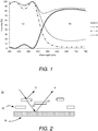
- the optical design of the article was modeled in an effort to maximize reflection where desired and prevent transmission everywhere else. Referring to FIG. 1 , the optical design shows the reflection curve 2, the transmittance curve 4, the square of transmittance 8, and the overall reflection 6; and the edge 10 between the reflection band and the transparent region.
- the reflection band 14 is an area around the center wavelength in which there is high reflectance 2 and low transmittance 4, and can be generally described in relation to this particular article, as to the right of the edge 10.
- the transparent region 12 is an area other than the reflection band 14, such as the wavelengths with low reflection 2 and high transmittance 4.
- FIG. 2 illustrates a composition including the article 20 dispersed in a liquid medium (not shown) applied onto a surface of a substrate 18.
- the overall reflected light from the optical device 16 would actually include the light 22 that is transmitted through the article 20 and reflected off the underlying substrate 18. Additionally, the same light that reflects off the substrate 20 can also pass through (e.g., light ray 24) another article 20.
- the maximum intensity of light is the square of transmittance (T 2 ) 8.
- the article having the stack of 5 transparent layers had poor hiding and low chromaticity.
- a method of forming an article can include depositing onto a substrate a stack of layers including a high refractive index layer and a low refractive index layer; wherein at least one layer of the stack includes a wavelength selective absorbing material; and wherein the stack of layers has a transparent region with an edge at a wavelength in which light is absorbed by the wavelength selective absorbing material, and a reflection band with an edge at a wavelength in which light is reflected.
- the stack of layers can be as described above.
- the substrate can be any suitable material that can be used in the composition and/or can be used in the method of forming an article.
- the substrate can include a release layer.
- the substrate for use in the optical device and the method can be made of a flexible material.
- substrate materials include polymer web, such as polyethylene terephthalate (PET), glass foil, glass sheets, polymeric foils, polymeric sheets, metal foils, metal sheets, ceramic foils, ceramic sheets, ionic liquid, paper, silicon wafers, etc.
- PET polyethylene terephthalate
- the substrate for use in the optical device can be different than the substrate for use in the method of making the article.
- the method can also include drying and curing, optionally after each deposition and before a next layer is deposited.
- the method can further include, after deposition of all of the layers, water stripping the release layer, if present, and the stack of layers, filtering the deposited layers, drying, and grinding to form the article, for example, a pigment, a flake, or a foil.
- the article can be formed using a liquid coating process for each layer.
- the liquid coating process can include, but is not limited to: slot-bead, slide bead, slot curtain, slide curtain, in single and multilayer coating, tensioned web slot, gravure, roll coating, and other liquid coating and printing processes that apply a layer onto a substrate or previously deposited layer to form a liquid layer or film that is subsequently dried and/or cured.
- a liquid coating process can allow for the accurate thickness control, for example, the liquid coating process can be used to deposit at least one layer in the stack of layers.
- at least one layer of the stack of layers can be a composition including a liquid medium and the wavelength selective absorbing material.
- the composition can include a polymer and nanoparticles of the wavelength selective absorbing materials.
- the article can be formed using evaporation processes for the deposition of each layer.
- a method of forming the article can include using a multi-channel slot die to apply two or more layers simultaneously and/or sequentially. This method can achieve a higher productivity with a less stages, such as a single stage.
- the layers of the stack that form the article may not require to be deposited under vacuum and thereby avoid the cost and loss of productivity associated with vacuum deposition techniques.
- the article can be subjected to a second drying and/or curing stage. The method may not use a vacuum step. The method can be used to form the articles discussed above with the layers discussed above.
- a method of making a composition can comprise dispersing the articles in a liquid medium to form the composition.
- Any suitable liquid medium can be used, such as polar or non-polar solvents.
- a suitable liquid medium include acetates, such as ethyl acetate, propyl acetate, and butyl acetate; acetone; water; ketones, such as dimethyl ketone (DMK), methylethyl ketone (MEK), sec-butyl methyl ketone (SBMK), ter-butyl methyl ketone (TBMK), cyclopenthanon, and anisole; glycol derivatives, such as propylene glycol methyl ether, and propylene glycol methyl ether acetate; alcohols, such as isopropyl alcohol, and diacetone alcohol; esters, such as malonates; heterocyclic solvents, such as n-methyl pyrrolidone; hydrocarbons, such as toluene, and xylene; coal
- a method of making an optical device can comprise applying to a surface of a substrate the composition.
- a substrate suitable for use in the method of making the optical device are disclosed above.
- the optical device can be used in a decorative application.
- nanoparticle(s) is understood to mean having a median particle size of less than about 500 nm, for example, from about 100 nm to about 300 nm, and as a further example less than about 100 nm.
Landscapes
- Physics & Mathematics (AREA)
- General Physics & Mathematics (AREA)
- Optics & Photonics (AREA)
- Chemical & Material Sciences (AREA)
- Chemical Kinetics & Catalysis (AREA)
- Engineering & Computer Science (AREA)
- Materials Engineering (AREA)
- Mechanical Engineering (AREA)
- Metallurgy (AREA)
- Organic Chemistry (AREA)
- Inorganic Chemistry (AREA)
- Laminated Bodies (AREA)
- Optical Filters (AREA)
- Optical Elements Other Than Lenses (AREA)
Abstract
Description
- The present disclosure generally relates to an article including a stack of layers including a high refractive index layer and a low refractive index layer; wherein at least one layer of the stack includes a wavelength selective absorbing material; and wherein the stack of layers has a transparent region with an edge at a wavelength in which light is absorbed by the wavelength selective absorbing material, and a reflection band with an edge at a wavelength in which light is reflected. A composition and an optical device including the article are also disclosed. Additionally, there is disclosed a method of making the article, the composition, and the optical device.
- Decorative pigment applications require low color travel, good hiding, and high flop. Conventional quarter wave stack designs have made use of transparent materials having low color travel, but they exhibit poor hiding and poor flop. Alternatively, decorative pigments based on Fabry-Perot structures use metal, such as thin layers of metal, which is generally made using vacuum deposition techniques thereby increasing the cost and time of manufacture. Moreover, the use of thin layers of metal increase the risk that the decorative pigment applications will be subject to corrosion over time.
- A quarter wave stack is a well-known optical design that is highly reflective within a range of the spectrum, but is transparent outside of this range. The region over which this design reflects can be selected by adjusting the thicknesses of the layers. The reflectivity in this region can even exceed the reflectivity afforded by metals, making this optical design attractive as a foundation for a special effect pigment.
- What is needed is different materials that can be used in decorative pigment applications so that light that would otherwise be transmitted can be absorbed while maintaining reflectivity, thereby resulting in an opaque design, but without the use of a metal layer.
- In an aspect, there is disclosed an article including a stack of layers including a high refractive index layer and a low refractive index layer; wherein at least one layer of the stack includes a wavelength selective absorbing material; and wherein the stack of layers has a transparent region with an edge at a wavelength in which light is absorbed by the wavelength selective absorbing material, and a reflection band with an edge at a wavelength in which light is reflected.
- The high refractive index layer may include the wavelength selective absorbing material.
- The low refractive index layer may include the wavelength selective absorbing material.
- Both the high refractive index layer and the low refractive index layer may include the wavelength selective absorbing material.
- The wavelength selective absorbing material may include a metal sulfide, a ternary system, a metal oxide, a pigment, a dye, and combinations thereof.
- The metal sulfide may be chosen from copper (I) sulfide, tin sulfide, nickel sulfide, silver sulfide, lead sulfide, molybdenum sulfide, iron disulfide, zinc sulfide, and combinations thereof.
- The ternary systems may include chalcopyrite and bornite.
- The metal oxides may include CuO, SiO2, TiO2, Al2O3, ZrO2, WO3, VO5, ITO, Ta2O5, CeO2, Y2O3, Sc2O3, ZnO, In2O3, La2O3, MgO, Nd2O3, Pr6O11, Fe2O3, Fe3O4, SiO, SnO2, FeOx, wherein x is an integer greater than 0, and their combinations.
- The stack may not include a thin layer of absorbing metal.
- The article may be opaque.
- The wavelength selective absorbing material may be a composite of a polymer and an absorbing pigment.
- In further aspects, there is disclosed a composition comprising the article dispersed in a liquid medium and an optical device comprising the composition applied to a surface of the substrate.
- In another aspect, there is disclosed a method of making an article, comprising: depositing onto a substrate a stack of layers including a high refractive index layer and a low refractive index layer; wherein at least one layer of the stack includes a wavelength selective absorbing material; and wherein the stack of layers has a transparent region with an edge at a wavelength in which light is absorbed by the wavelength selective absorbing material, and a reflection band with an edge at a wavelength in which light is reflected.
- The article may exhibit at least one property chosen from good hiding, high flop, or low color travel.
- The method may further comprise drying and curing each layer of the stack before a next layer of the stack is deposited.
- A liquid coating process may be used to deposit at least one layer in the stack of layers.
- An evaporation process may be used to deposit each layer.
- The layers of the stack may not require deposition under vacuum.
- In a further aspect, there is disclosed a method of making a composition comprising dispersing the article of the first aspect in a liquid medium.
- Additional features and advantages of various embodiments will be set forth, in part, in the description that follows, and will, in part, be apparent from the description, or can be learned by the practice of various embodiments. The objectives and other advantages of various embodiments will be realized and attained by means of the elements and combinations particularly pointed out in the description herein.
- The present disclosure in its several aspects and embodiments can be more fully understood from the detailed description and the accompanying drawings, wherein:
-
FIG. 1 is a graph illustrating the reflectance and transmittance of a convention quarter wave reflector including transparent materials; -
FIG. 2 is a graphical illustrating overall reflectance for a pigment; -
FIG. 3 is a graph illustrating the tin sulfide constants; -
FIG. 4 is a graph illustrating the simulated performance of a 5-layer article of tin sulfide and magnesium fluoride; -
FIG. 5 is a graph illustrating the transmission and reflection data of the article ofFIG. 4 , after it was coated on PET with a hard coat; -
FIG. 6 is a graph comparing draw-drown overall reflection for various pigments including on white and black regions; -
FIG. 7 is a graph comparing a computer simulation to draw down measurements for various pigments; -
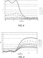
FIG. 8 is a graph illustrating how overall transmission varies for different extinction coefficients; -
FIG. 9 is a graph illustrating reflection for various extinction coefficients; -
FIG. 10 is a graph illustrating how overall reflection varies for different extinction coefficients; -
FIG. 11 is a graph illustrating reflection curves for a pigment with a color shift from 0 degrees to 60 degrees; -
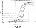
FIG. 12 is a graph illustrating reflection curves for a pigment with a low index polymer and a high index composite with a color shift from 0 degrees to 60 degrees; and -
FIG. 13 is a graph illustrating reflection curves for a pigment similar to the one inFIG. 12 , but including pigment red with the low index polymer. - Throughout this specification and figures like reference numbers identify like elements.
- It is to be understood that both the foregoing general description and the following detailed description are exemplary and explanatory only, and are intended to provide an explanation of various embodiments of the present teachings. The layers/components shown in each Figure may be described with regard to a particular Figure, but it is understood that the description of a particular layer/component would be applicable to the equivalent layer/component in the other Figures.
- In its broad and varied embodiments, disclosed herein is an article comprising a stack of layers including a high refractive index layer and a low refractive index layer; wherein at least one layer of the stack includes a wavelength selective absorbing material; and wherein the stack of layers has a transparent region with an edge at a wavelength in which light is absorbed by the wavelength selective absorbing material, and a reflection band with an edge at a wavelength in which light is reflected.
- The article can be in a form of a flake, a pigment, or a foil. The pigment can be a special effect pigment. The article can be opaque. The article can be dispersed in a liquid medium to form a composition, such as an ink or paint. The composition can be applied to a substrate to form an optical device. The article can exhibit at least one property chosen from high flop (i.e., a measure of the change in lightness of a color as it is tilted through a range of viewing angles, in which "high" is greater than or equal to 10, for example, about 35, and as a further example, in a range from about 10 to about 35, such as from about 20 to about 30., low color travel (as compared to Fabry-Perot designs), or good hiding. The article, composition, and optical device will be described more fully below, as well as methods of making each.
- The article can include a stack of layers including a high refractive (H) index layer and a low refractive (L) index layer. In forming the article, care should be taken to bifurcate the layers of the stack to preserve a difference in the refraction index of each layer, which can drive the reflectivity of the article. The stack can have a bottom layer, one or more middle layers, and a top layer, in which it is understood that the words "bottom" and "top" are used for ease of reference and are not limiting as to placement in the stack. In an aspect, the bottom layer and the top layer can both be low refractive index layers. In an aspect, the bottom layer and the top layer can both be high refractive index layers. In an aspect, the bottom layer can be a low refractive index layer and the top layer can be a high refractive index layer or vice versa. In another aspect, the stack of layers includes an odd number of alternating layers, for example, 3 alternating layers, 5 alternating layers, 7 alternating layers, and 9 alternating layers. For example, the article can be a stack of 5 layers with MgF2 and copper (II) sulfide. In another aspect, the stack of layers includes an even number of alternating layers, for example, 4 alternating layers, 6 alternating layers, 8 alternating layers, and 10 alternating layers. The stack can have the formula (HLH)n, in which n is an integer greater than or equal to 1.
- At least one layer of the stack can include a wavelength selective absorbing material. The at least one layer of the stack can include two or more different wavelength selective absorbing materials. Additionally, and/or alternatively, the stack can include two or more different wavelength selective absorbing materials, for example, in the same or different layers of the stack. In an aspect, a high refractive index layer of the stack can include the wavelength selective absorbing material. In another aspect, a low refractive index layer of the stack can include the wavelength selective absorbing material. In a further aspect, both the high refractive index layer and the low refractive index layers include the wavelength selective absorbing material. In this manner, the refractive index of each layer in the stack can be tuned. Similarly, the absorption of light in each layer can be tuned. In an aspect, the stack does not include a thin layer of absorbing metal.
- The high refractive index layer can also include a high refractive index material, i.e., having a refractive index greater than greater than about 1.65. Non-limiting examples of high refractive index materials include zinc sulfide (ZnS), zinc oxide (ZnO), zirconium oxide (ZrO2), titanium dioxide (TiO2), diamond-like carbon, indium oxide (In2O3), indium-tin-oxide (ITO), tantalum pentoxide (Ta2O5), cerium oxide (CeO2), yttrium oxide (Y2O3), europium oxide (Eu2O3), iron oxides such as (II)diiron(III) oxide (Fe3O4) and ferric oxide (Fe2O3), hafnium nitride (HfN), hafnium carbide (HfC), hafnium oxide (HfO2), lanthanum oxide (La2O3), magnesium oxide (MgO), neodymium oxide (Nd2O3), praseodymium oxide (Pr6O11), samarium oxide (Sm2O3), antimony trioxide (Sb2O3), silicon, silicon monoxide (SiO), selenium trioxide (Se2O3), tin oxide (SnO2), tungsten trioxide (WO3), or their combinations.
- The low refractive index layer can also include a low refractive index material, i.e., having a refractive index less than about 1.65. Non-limiting examples of low refractive index materials include silicon dioxide (SiO2), aluminum oxide (Al2O3), metal fluorides such as magnesium fluoride (MgF2), aluminum fluoride (AlF3), cerium fluoride (CeF3), lanthanum fluoride (LaF3), sodium aluminum fluorides (e.g., Na3AlF6 or Na5Al3F14), neodymium fluoride (NdF3), samarium fluoride (SmF3), barium fluoride (BaF2), calcium fluoride (CaF2), lithium fluoride (LiF), or their combinations. Organic monomers and polymers can be utilized as low refractive index materials, including dienes or alkenes such as acrylates (e.g., methacrylate), perfluoroalkenes, polytetrafluoroethylene (Teflon), fluorinated ethylene propylene (FEP), or their combinations thereof.
- In the article, one or more layers of the stack can include a wavelength selective absorbing material. In an aspect, the wavelength selective absorbing material can be dispersed in a liquid medium for deposition as a layer in a liquid coating process. The wavelength selective absorbing material can include a metal sulfide, a ternary system, a metal oxide, a pigment, a dye, and combinations thereof. In an aspect, the wavelength selective absorbing material can be a composite of a polymer material and an absorbing pigment. A wavelength absorbing material can have minimal absorption where reflection is desired. A wavelength absorbing material can also limit color travel as compared to a pigment constructed with a Fabry-Perot structure.
- The wavelength selective absorbing material can be a metal oxide. Non-limiting examples of a metal oxide include CuO, SiO2, TiO2, Al2O3, ZrO2, WO3, VO5, ITO, Ta2O5, CeO2, Y2O3, Sc2O3, ZnO, In2O3, La2O3, MgO, Nd2O3, Pr6O11, Fe2O3, Fe3O4, SiO, SnO2, FeOx(where x is an integer greater than 0), and their combinations.
- The wavelength selective absorbing material can be a metal sulfide. Non-limiting examples of a metal sulfide include copper (I) sulfide, tin sulfide, nickel sulfide, silver sulfide, lead sulfide, molybdenum sulfide, iron disulfide, zinc sulfide, or combinations thereof. Complex ternary systems can also be used such as chalcopyrite and bornite.
- The wavelength selective absorbing material can be an organic colored material, such as a dye. Any dye recognized in the Colour Index™ published by the Society of Dyers and Colourists can be used. Non-limiting examples of an organic colored material include carbon, graphite, perylene, perinone, quinacridone, pyrrole, quinacridonequinone, anthrapyrimidine, anthraquinone, anthanthrone, benzimidazolone, disazo condensation, azo, quinolones, xanthene, azomethine, quinophthalone, indanthrone, phthalocyanine, triarylcarbonium, dioxazine, aminoanthraquinone, isoindoline, diketopyrrolopyrrole, thioindigo, thiazineindigo, isoindolinone, pyranthrone, isoviolanthrone, miyoshi methane, triarylmethane, or mixtures thereof. The organic colored material can also be cobalt green, cobalt blue, Prussian blue, and manganese violet.
- The wavelength selective absorbing material can be a pigment, such as an absorbing pigment. Any pigment recognized in the Colour Index™ published by the Society of Dyers and Colourists can be used. Non-limiting examples of pigments include C.I. Pigment Red 123 (C.I. No. 71 145), C.I. Pigment Red 149 (C.I. No. 71 137), C.I. Pigment Red 178 (C.I. No. 71 155), C.I. Pigment Red 179 (C.I. No. 71 130), C.I. Pigment Red190 (C.I. 71 140), C.I. Pigment Red 224 (C.I. No. 71 127), C.I. Pigment Violet 29 (C.I. No. 71 129), C.I. Pigment Orange 43 (C.I. No. 71 105), C.I. Pigment Red 194 (C.I. No. 71 100), C.I. Pigment Violet 19 (C.I. No. 73 900), C.I. Pigment Red 122 (C.I. No. 73 915), C.I. Pigment Red 192, C.I. Pigment Red 202 (C.I. No. 73 907), C.I. Pigment Red 207, C.I. Pigment Red 209 (C.I. No. 73 905), C.I. Pigment Red 206 (C.I. No. 73 900/73 920), C.I. Pigment Orange 48 (C.I. No. 73 900/73 920), C.I. Pigment Orange 49 (C.I. No. 73 900/73 920), C.I. Pigment Orange 42, C.I. Pigment Yellow 147, C.I. Pigment Red 168 (C.I. No. 59 300), C.I. Pigment Yellow 120 (C.I. No. 11 783), C.I. Pigment Yellow 151 (C.I. No. 13 980), C.I. Pigment Brown 25 (C.I. No. 12 510), C.I. Pigment Violet 32 (C.I. No. 12 517), C.I. Pigment Orange 64; C.I. Pigment Brown 23 (C.I. No. 20 060), C.I. Pigment Red 166 (C.I. No. 20 730), C.I. Pigment Red 170 (C.I. No. 12 475), C.I. Pigment Orange 38 (C.I. No. 12 367), C.I. Pigment Red 188 (C.I. No. 12 467), C.I. Pigment Red 187 (C.I. No. 12 486), C.I. Pigment Orange 34 (C.I. No. 21 115), C.I. Pigment Orange 13 (C.I. No. 21 110), C.I. Pigment Red 9 (C.I. No. 12 460), C.I. Pigment Red 2 (C.I. No. 12 310), C.I. Pigment Red 112 (C.I. No. 12 370), C.I. Pigment Red 7 (C.I. No. 12 420), C.I. Pigment Red 210 (C.I. No. 12 477), C.I. Pigment Red 12 (C.I. No. 12 385), C.I. Pigment Blue 60 (C.I. No. 69 800), C.I. Pigment Green 7 (C.I. No. 74 260), C.I. Pigment Green 36 (C.I. No. 74 265); C.I. Pigment Blue 15:1, 15:2, 15:3, 15:4, 15:6 and 15 (C.I. No. 74 160); C.I. Pigment Blue 56 (C.I. No. 42 800), C.I. Pigment Blue 61 (C.I. No. 42 765:1), C.I. Pigment Violet 23 (C.I. No. 51 319), C.I. Pigment Violet 37 (C.I. No. 51 345), C.I. Pigment Red 177 (C.I. No. 65 300), C.I. Pigment Red 254 (C.I. No. 56 110), C.I. Pigment Red 255 (C.I. No. 56 1050), C.I. Pigment Red 264, C.I. Pigment Red 270, C.I. Pigment Red 272 (C.I. No. 56 1150), C.I. Pigment Red 71, C.I. Pigment Orange 73, C.I. Pigment Red 88 (C.I. No. 73 312), C.I. Pigment Yellow 175 (C.I. No. 11 784), C.I. Pigment Yellow 154 (C.I. No. 11 781), C.I. Pigment Yellow 83 (C.I. No. 21 108), C.I. Pigment Yellow 180 (C.I. No. 21 290), C.I. Pigment Yellow 181 (C.I. No. 11 777), C.I. Pigment Yellow 74 (C.I. No. 11 741), C.I. Pigment Yellow 213, C.I. Pigment Orange 36 (C.I. No. 11 780), C.I. Pigment Orange 62 (C.I. No. 11 775), C.I. Pigment Orange 72, C.I. Pigment Red 48:2/3/4 (C.I. No. 15 865:2/3/4), C.I. Pigment Red 53:1 (C.I. No. 15 585:1), C.I. Pigment Red 208 (C.I. No. 12 514), C.I. Pigment Red 185 (C.I. No. 12 516), C.I. Pigment Red 247 (C.I. No. 15 915), Pigment Black 31 (C40H26N2O4), Pigment Orange 16 (C32H24C12N8O2), or combinations thereof.
- In the article, the stack of layers can have a transparent region with an edge at a wavelength in which light is absorbed by the wavelength selective absorbing material, and a reflection band with an edge at a wavelength in which light is reflected. The transparent region and the reflection band of the article are explained below. In an aspect, a wavelength selective absorbing material can have limited to no absorption where the reflectance should be maximal, and controlled absorption outside of the reflection band.
- COMPARATIVE EXAMPLE - An article was prepared having a stack of 5 transparent layers, i.e., three high refractive index layers, in which n = 2.3, and two low refractive index layers, in which n = 1.3; and was centered at 700 nm. The optical design of the article was modeled in an effort to maximize reflection where desired and prevent transmission everywhere else. Referring to
FIG. 1 , the optical design shows thereflection curve 2, thetransmittance curve 4, the square oftransmittance 8, and theoverall reflection 6; and theedge 10 between the reflection band and the transparent region. Thereflection band 14 is an area around the center wavelength in which there ishigh reflectance 2 andlow transmittance 4, and can be generally described in relation to this particular article, as to the right of theedge 10. Thetransparent region 12 is an area other than thereflection band 14, such as the wavelengths withlow reflection 2 andhigh transmittance 4. - However, it is noted that an
optical device 16 prepared with the article designed inFIG. 1 , would not have thesame reflection curve 2, but would instead have theoverall reflection curve 6.FIG. 2 illustrates a composition including thearticle 20 dispersed in a liquid medium (not shown) applied onto a surface of asubstrate 18. The overall reflected light from theoptical device 16 would actually include the light 22 that is transmitted through thearticle 20 and reflected off the underlyingsubstrate 18. Additionally, the same light that reflects off thesubstrate 20 can also pass through (e.g., light ray 24) anotherarticle 20. The maximum intensity of light is the square of transmittance (T2) 8. The overall reflection (OAR) 6 is therefore the sum of theinitial reflection 2 and thesquare transmittance 8; OAR = R + T2. The article having the stack of 5 transparent layers had poor hiding and low chromaticity. - EXAMPLE 1 - An article including a stack of layers of high refractive index layers and low refractive index layers was made. At least one layer of the stack included a wavelength selective absorbing material, such as copper sulfide, tin sulfide, or iron oxide as a high refractive index material; and magnesium fluoride as a low refractive index material. As shown in
FIG. 3 , tin sulfide can be used as wavelength selective absorbing material because it absorbs strongly at short wavelengths and less strongly at longer wavelengths. Another exemplary wavelength selective absorbing material would have little to no absorption in the reflection band.
FIG. 4 shows the simulated optical performance of an article prepared having a stack of 5 layers of tin sulfide and magnesium fluoride; and was centered at 850 nm. The simulation used the measured values for absorption (solid lines lines reflectance 2a. When the absorbance was turned off in the simulation, the transmittedlight 8 had a major effect on the overall reflectedlight 6 and was comparable to thereflectance 2. Tin sulfide absorbed over all wavelengths shown and negatively impacts the desired reflectance in thereflection band 630 nm - 780 nm.
This example showed that when there is no absorption (i.e., when the absorption for tin sulfide was turned off in the simulation, e.g., dotted lines), the effects are similar to those in the Comparative Example using transparent layers, as shown inFIG. 1 . In particular, light that is transmitted through thearticle 20 and reflected off the object 8 (FIGs. 1 and4 ) had a significant effect on theoverall reflectance 6. However, when wavelength selective absorbing material was used, the overall reflection yielded a red appearance 6a. It is noted that because tin sulfide is a high refractive, wavelength selective absorbing material, and its reflectance 6a remains higher than others at shorter wavelengths (600 nm and shorter). Use of a different wavelength selective absorbing material could reduce this reflectivity. - EXAMPLE 2 - An
optical device 16 was prepared with aPET substrate 18, thearticle 20 from Example 1 in the form of a foil, and a hard coat. Thetransmission 4 and reflection from both sides (2c, 2d) was obtained. Theoverall reflection 6 was calculated after averaging 2c and 2d. The simulation shown inFIG. 5 was performed immersed in a liquid medium having a low refractive index of 1.5 while the foil was measured in air and only the PET side had a comparably high refractive index. Qualitatively, there was good agreement between the simulation and the experimental results. Both the simulation and foil had high reflectivity at longer wavelengths and lower reflectivity at shorter wavelengths. The foil did have a higher transmission with a peak around 600 nm that was not predicted in the simulation. This likely reflected inaccuracy in the refractive index data obtained for tin sulfide or process variations that have led to a difference in the optical constants for tin sulfide. The refractive index data was generated using a Variable Angle Spectral Ellipsometer (VASE).
The data can be used to predict how this article would perform as a composition. The tworeflectivity curves 2c, 2d were averaged and theoverall reflection 6 was calculated. The composition was stripped and drawdowns were prepared. The drawdowns were measured on the Hitachi spectrophotometer and the results showed good agreement with the simulation inFIG. 5 . The reflectivity was lower than calculated because the predicted reflection curve was calculated from measurements taken in air. Another important point to note is the measurements between the white and black regions of the Leneta card do not vary. This was proof of good hiding. - EXAMPLE 3 - Three five-layer stacks were simulated centered at 450 nm, 650 nm, and 780 nm. Because iron oxide is significantly less absorbing at longer wavelengths, it was expected that the design centered at 450 nm would have leakage at longer wavelengths. Conversely, designs centered at the longer wavelengths would meet the design criteria for the new pigment described in this report and thus would have good hiding.
Using transmittance and reflectance data measured on the coated foils, theoverall reflectance 6 of an article was calculated (as shown inFIG.6 , e.g., "6-450" is the overall reflectance for the stack centered at 450 nm). The foils were converted to pigment and drawdowns were prepared. Color measurements (Hunter spectrophotometer) were made on the white (dotted lines) and black regions (dashed lines) of the Leneta card for each drawdown. For each pigment design, the measurements over each region (black and white) coincided almost perfectly (e.g., "6-450 DD" is the overall reflectance for the optical device), indicating each pigment exhibited good hiding. The measured reflectance also closely matched the shape of the reflectance predicted from foil measurements, though with some losses attributable to the conversion from a flat foil to slightly misaligned flakes. Universally, it is seen that the reflectance of a design decreases when the foil is converted to pigment and this shows the difference between a smooth planar surface and air. - EXAMPLE 4 - The same pigments used in Example 3 were used so that the overall reflection predicted by DECO (e.g., "6-450" dotted line) was compared to the draw down measurements (e.g. "6-450" solid line). Two differences are observed. First, the blue pigment design centered at 450 nm had more hiding than expected, for example, at wavelengths longer than 680 nm. Second, the red pigment had a lower reflectance at longer wavelengths. Both of these results can be explained if the iron oxide coated during these runs had high absorption at longer wavelengths than the iron oxide coating used to obtain refractive index data (obtained by VASE). Regardless, this experiment produced a novel and surprising result. Iron oxide, normally thought of as a "red" material, could be used to produce a range of colors including blue.
- EXAMPLE 5 - In developing a suitable article, a key driver is the difference between the refractive indices of the layers of the stack. For example, two layers with a small difference in refractive index could lead to poor performance or necessitate numerous layers to achieve the same property, such as reflectivity. Table 1 below shows the calculated reflectance for a 5-layer article centered at 550 nm. As can be seen, the reflectance is maximized when the difference between the indices is maximized (e.g., a high refractive index of 2.5 and a low refractive index of 1.3 has a reflectance of 90).
The use of a 7-layer design further increased the reflectivity. Adding layers to the stack increased reflectance. For example, a 7-layer design with 89% R can be achieved with wavelength selective absorbing materials with indices of 1.3 (low) and 2.1 (high) as compared to a 5-layer design.
 The wavelength selective absorbing materials should be added in a way that increases or preserves the difference in the refractive index between the layers of the stack. For instance, an inorganic with an index around 1.9 would be more effective in a high refractive index layer while an organic dye with an index around 1.5 would be more effective in a low refractive index layer.
- EXAMPLE 6 - To illustrate the impact absorption has in the reflection band and outside the reflection band, the following simulations were performed. The performance in the reflection band should be evaluated separately from the performance in the transparent region. In the simulations that follow, the reflection band is greater than or equal to 580 nm and the transparent region is less than 580 nm.
Theoverall transmission 8 is the easiest of these plots to understand (FIG. 8 ). Theoverall transmission 8 was plotted rather than theactual transmission 4 because light reflected off a painted surface will realistically be transmitted twice or more according to the model discussed in the earlier section. Thus, theoverall transmission 8 of the article is the maximum contributed from the light not originally reflected.
With k=0 for the high index material, very high transmission occurred. Increasing absorption (k > 0) further diminished transmission, as expected. However, once k=0.5 was reached, a point of diminishing return was found. Above 580 nm, the transmission was low as this corresponded to the reflection band. - EXAMPLE 7 - The related reflectivity plot is shown in
FIG. 9 . As shown, above 580 nm where the article is highly reflective, i.e., the reflection band, increasing the absorption decreased the reflectivity. The effect of absorption was more interesting in the transparent region, i.e., less than 580 nm. It can be seen that the reflectivity initially decreased with increasing absorption until k is 0.2. With further increases in k, the reflectivity in this region actually increased. This point is likely not intuitive, as one would assume increasing absorption at wavelengths where light is undesired would reduce their intensity in the overall reflection and improve performance; in actuality, increasing absorption can boost reflectivity and lower chromaticity. - EXAMPLE 8 - The data in
FIGs. 8 and 9 were combined intoFIG. 10 to understand theoverall reflectivity 6 of an article for various k. As discussed above, at wavelengths longer than 580 nm where the article is reflective, it is desirable to have very low absorption. At wavelengths shorter than 580 nm where the article is expected to be transparent, moderate absorption is desired. As shown inFIG. 10 , chromaticity was optimized when k = 0.5. Values of k lower than 0.5 lead to increased reflection of the transmitted light while values of k greater than 0.5 led to boosted reflectivity. - EXAMPLE 9 - An article was prepared having 7 layers with a high refractive index layer (n = 2.2) including copper phthalocyanine blue (30% volume) and titania (70% volume); the low refractive index layer includes a polymer with n = 1.4 with no absorption.
FIG. 11 shows the reflection curves 2 plotted for angles from 0 degrees to 60 degrees. - EXAMPLE 10 - An article was prepared having 7 layers with a high refractive index layer including a composite with iron oxide (30% volume) and titania (70% volume); the low refractive index layer includes a polymer with n = 1.4 with no absorption.
FIG. 12 shows the reflection curves 2 plotted for angles from 0 degrees to 60 degrees. - EXAMPLE 11 - An article similar to the article of Example 10 was prepared except that 30% volume DPP254 (red pigment) was added to the low refractive index layer.
FIG. 13 shows the reflection curves 2 plotted for angles from 0 degrees to 60 degrees. The article reflected less of the unwanted light between 500 and 600 nm. - A method of forming an article can include depositing onto a substrate a stack of layers including a high refractive index layer and a low refractive index layer; wherein at least one layer of the stack includes a wavelength selective absorbing material; and wherein the stack of layers has a transparent region with an edge at a wavelength in which light is absorbed by the wavelength selective absorbing material, and a reflection band with an edge at a wavelength in which light is reflected. The stack of layers can be as described above.
- The substrate can be any suitable material that can be used in the composition and/or can be used in the method of forming an article. The substrate can include a release layer. The substrate for use in the optical device and the method can be made of a flexible material. Non-limiting examples of substrate materials include polymer web, such as polyethylene terephthalate (PET), glass foil, glass sheets, polymeric foils, polymeric sheets, metal foils, metal sheets, ceramic foils, ceramic sheets, ionic liquid, paper, silicon wafers, etc. In an aspect, the substrate for use in the optical device can be different than the substrate for use in the method of making the article.
- The method can also include drying and curing, optionally after each deposition and before a next layer is deposited. The method can further include, after deposition of all of the layers, water stripping the release layer, if present, and the stack of layers, filtering the deposited layers, drying, and grinding to form the article, for example, a pigment, a flake, or a foil.
- The article can be formed using a liquid coating process for each layer. The liquid coating process can include, but is not limited to: slot-bead, slide bead, slot curtain, slide curtain, in single and multilayer coating, tensioned web slot, gravure, roll coating, and other liquid coating and printing processes that apply a layer onto a substrate or previously deposited layer to form a liquid layer or film that is subsequently dried and/or cured. A liquid coating process can allow for the accurate thickness control, for example, the liquid coating process can be used to deposit at least one layer in the stack of layers. Additionally, with a liquid coating process at least one layer of the stack of layers can be a composition including a liquid medium and the wavelength selective absorbing material. For example, the composition can include a polymer and nanoparticles of the wavelength selective absorbing materials.
- In another aspect, the article can be formed using evaporation processes for the deposition of each layer.
- In an aspect, a method of forming the article can include using a multi-channel slot die to apply two or more layers simultaneously and/or sequentially. This method can achieve a higher productivity with a less stages, such as a single stage. In the disclosed method, the layers of the stack that form the article may not require to be deposited under vacuum and thereby avoid the cost and loss of productivity associated with vacuum deposition techniques. The article can be subjected to a second drying and/or curing stage. The method may not use a vacuum step. The method can be used to form the articles discussed above with the layers discussed above.
- A method of making a composition can comprise dispersing the articles in a liquid medium to form the composition. Any suitable liquid medium can be used, such as polar or non-polar solvents. Non-limiting examples of a suitable liquid medium include acetates, such as ethyl acetate, propyl acetate, and butyl acetate; acetone; water; ketones, such as dimethyl ketone (DMK), methylethyl ketone (MEK), sec-butyl methyl ketone (SBMK), ter-butyl methyl ketone (TBMK), cyclopenthanon, and anisole; glycol derivatives, such as propylene glycol methyl ether, and propylene glycol methyl ether acetate; alcohols, such as isopropyl alcohol, and diacetone alcohol; esters, such as malonates; heterocyclic solvents, such as n-methyl pyrrolidone; hydrocarbons, such as toluene, and xylene; coalescing solvents, such as glycol ethers; and mixtures thereof. The liquid medium can be an organic matrix. The liquid medium can have a low refractive index. The composition can be an ink or a paint vehicle.
- A method of making an optical device can comprise applying to a surface of a substrate the composition. Non-limiting examples of a substrate suitable for use in the method of making the optical device are disclosed above. The optical device can be used in a decorative application.
- For the purpose of the application, "nanoparticle(s)" is understood to mean having a median particle size of less than about 500 nm, for example, from about 100 nm to about 300 nm, and as a further example less than about 100 nm.
- From the foregoing description, those skilled in the art can appreciate that the present teachings can be implemented in a variety of forms. Therefore, while these teachings have been described in connection with particular embodiments and examples thereof, the true scope of the present teachings should not be so limited. Various changes and modifications can be made without departing from the scope of the teachings herein.
- This scope disclosure is to be broadly construed. It is intended that this disclosure disclose equivalents, means, systems and methods to achieve the devices, activities and mechanical actions disclosed herein. For each device, article, method, mean, mechanical element or mechanism disclosed, it is intended that this disclosure also encompass in its disclosure and teaches equivalents, means, systems and methods for practicing the many aspects, mechanisms and devices disclosed herein. Additionally, this disclosure regards a coating and its many aspects, features and elements. Such a device can be dynamic in its use and operation, this disclosure is intended to encompass the equivalents, means, systems and methods of the use of the device and/or optical device of manufacture and its many aspects consistent with the description and spirit of the operations and functions disclosed herein. The claims of this application are likewise to be broadly construed. The description of the inventions herein in their many embodiments is merely exemplary in nature and, thus, variations that do not depart from the gist of the invention are intended to be within the scope of the invention. Such variations are not to be regarded as a departure from the spirit and scope of the invention.
Claims (15)
- An article, comprising:a stack of layers including a high refractive index layer and a low refractive index layer;wherein at least one layer of the stack includes a wavelength selective absorbing material; andwherein the stack of layers has a transparent region with an edge at a wavelength in which light is absorbed by the wavelength selective absorbing material, and a reflection band with an edge at a wavelength in which light is reflected by the wavelength selective absorbing material.
- The article of claim 1, wherein the high refractive index layer includes the wavelength selective absorbing material.
- The article of claim 1 or claim 2, wherein the low refractive index layer includes the wavelength selective absorbing material.
- The article of any of claims 1 to 3, wherein the wavelength selective absorbing material includes a metal sulfide, a ternary system, a metal oxide, a pigment, a dye, and combinations thereof.
- The article of claim 4, wherein the metal sulfide is chosen from copper (I) sulfide, tin sulfide, nickel sulfide, silver sulfide, lead sulfide, molybdenum sulfide, iron disulfide, zinc sulfide, and combinations thereof.
- The article of claim 4, wherein the ternary systems include chalcopyrite and bornite.
- The article of claim 4, wherein the metal oxides include CuO, SiO2, TiO2, Al2O3, ZrO2, WO3, VO5, ITO, Ta2O5, CeO2, Y2O3, Sc2O3, ZnO, In2O3, La2O3, MgO, Nd2O3, Pr6O11, Fe2O3, Fe3O4, SiO, SnO2, FeOx, wherein x is an integer greater than 0, and their combinations.
- The article of any of claims 1 to 7, wherein the stack does not include a thin layer of absorbing metal.
- The article of any of claims 1 to 8, wherein the article is opaque.
- The article of any of claims 1 to 9, wherein the wavelength selective absorbing material is a composite of a polymer and an absorbing pigment.
- A composition, comprising:
the article of any of claims 1 to 10 dispersed in a liquid medium. - An optical device, comprising:
the composition of claim 11 applied to a surface of a substrate. - A method of making an article, comprising:depositing onto a substrate a stack of layers including a high refractive index layer and a low refractive index layer;wherein at least one layer of the stack includes a wavelength selective absorbing material; andwherein the stack of layers has a transparent region with an edge at a wavelength in which light is absorbed by the wavelength selective absorbing material, and a reflection band with an edge at a wavelength in which light is reflected.
- The method of claim 13, further comprising drying and curing each layer of the stack before a next layer of the stack is deposited; and/orwherein a liquid coating process is used to deposit at least one layer in the stack of layers or an evaporation process is used to deposit each layer; and/orwherein the layers of the stack do not require deposition under vacuum.
- A method of making a composition comprising dispersing the article of any of claims 1 to 10 in a liquid medium.
Applications Claiming Priority (1)
| Application Number | Priority Date | Filing Date | Title |
|---|---|---|---|
| US16/918,698 US11892663B2 (en) | 2020-07-01 | 2020-07-01 | Article including a wavelength selective absorbing material |
Publications (3)
| Publication Number | Publication Date |
|---|---|
| EP3933463A2 true EP3933463A2 (en) | 2022-01-05 |
| EP3933463A3 EP3933463A3 (en) | 2022-03-30 |
| EP3933463B1 EP3933463B1 (en) | 2026-03-25 |
Family
ID=76584441
Family Applications (1)
| Application Number | Title | Priority Date | Filing Date |
|---|---|---|---|
| EP21181264.9A Active EP3933463B1 (en) | 2020-07-01 | 2021-06-23 | An article including a wavelength selective absorbing material |
Country Status (3)
| Country | Link |
|---|---|
| US (1) | US11892663B2 (en) |
| EP (1) | EP3933463B1 (en) |
| CN (1) | CN113885117B (en) |
Cited By (1)
| Publication number | Priority date | Publication date | Assignee | Title |
|---|---|---|---|---|
| CN116332137A (en) * | 2023-01-05 | 2023-06-27 | 南京信息工程大学 | A kind of multi-element metal selenide absorbing material and preparation method thereof |
Families Citing this family (5)
| Publication number | Priority date | Publication date | Assignee | Title |
|---|---|---|---|---|
| KR102894158B1 (en) | 2019-01-07 | 2025-12-01 | 비아비 솔루션즈 아이엔씨. | Multilayer articles containing organic layers |
| US12613366B2 (en) | 2020-04-06 | 2026-04-28 | Viavi Solutions Inc. | Article including a stack of alternating layers |
| US12504571B2 (en) | 2020-04-06 | 2025-12-23 | Viavi Solutions Inc. | Article including two external layers of absorbing nanoparticles |
| US12271011B2 (en) * | 2020-09-18 | 2025-04-08 | Viavi Solutions Inc. | Diffractive pigment including an embossed layer |
| CN116009128B (en) * | 2022-12-26 | 2025-03-25 | 巨玻固能(苏州)薄膜材料有限公司 | Black optical films and optical products |
Family Cites Families (8)
| Publication number | Priority date | Publication date | Assignee | Title |
|---|---|---|---|---|
| US6686042B1 (en) | 2000-09-22 | 2004-02-03 | Flex Products, Inc. | Optically variable pigments and foils with enhanced color shifting properties |
| US7238424B2 (en) | 2002-05-31 | 2007-07-03 | Jds Uniphase Corporation | All-dielectric optically variable pigments |
| US20070097509A1 (en) | 2005-10-31 | 2007-05-03 | Nevitt Timothy J | Optical elements for high contrast applications |
| DE102009037932A1 (en) | 2009-08-19 | 2011-02-24 | Eckart Gmbh | High gloss multi-layer pearlescent pigments with narrow size distribution and process for their preparation |
| CN106461834B (en) * | 2014-04-01 | 2021-01-15 | 丰田自动车工程及制造北美公司 | Color-shifting free multilayer structure |
| CN108291986B (en) | 2015-10-13 | 2021-01-05 | 视觉缓解公司 | Optical filter with selective transmittance and reflectance |
| JP6837930B2 (en) | 2016-06-27 | 2021-03-03 | ヴァイアヴィ・ソリューションズ・インコーポレイテッドViavi Solutions Inc. | High chromaticity flakes |
| ES2902754T3 (en) | 2018-07-27 | 2022-03-29 | Cnbm Bengbu Design & Res Institute For Glass Industry Co Ltd | Solar module with structured cover plate and optical interference layer |
-
2020
- 2020-07-01 US US16/918,698 patent/US11892663B2/en active Active
-
2021
- 2021-06-23 EP EP21181264.9A patent/EP3933463B1/en active Active
- 2021-06-29 CN CN202110726838.9A patent/CN113885117B/en active Active
Cited By (2)
| Publication number | Priority date | Publication date | Assignee | Title |
|---|---|---|---|---|
| CN116332137A (en) * | 2023-01-05 | 2023-06-27 | 南京信息工程大学 | A kind of multi-element metal selenide absorbing material and preparation method thereof |
| CN116332137B (en) * | 2023-01-05 | 2024-05-24 | 南京信息工程大学 | A multi-element metal selenide absorbing material and preparation method thereof |
Also Published As
| Publication number | Publication date |
|---|---|
| US20220003905A1 (en) | 2022-01-06 |
| CN113885117A (en) | 2022-01-04 |
| EP3933463A3 (en) | 2022-03-30 |
| US11892663B2 (en) | 2024-02-06 |
| CN113885117B (en) | 2024-08-16 |
| EP3933463B1 (en) | 2026-03-25 |
Similar Documents
| Publication | Publication Date | Title |
|---|---|---|
| EP3933463B1 (en) | An article including a wavelength selective absorbing material | |
| JP7796786B2 (en) | Optical tools with azimuth-modulating layers. | |
| JP7166223B2 (en) | Optical tool with colored reflective layer | |
| US6997981B1 (en) | Thermal control interface coatings and pigments | |
| KR100446049B1 (en) | Infrared absorption filter | |
| CN111761897B (en) | Absorption Interference Type All-Dielectric Structural Color Films | |
| CN114746513A (en) | Composition containing color-changing pigments with different particle sizes | |
| CN1451029A (en) | Color shifting carbon-containing interference pigments | |
| JP2004510013A (en) | Optically variable pigments and foils with enhanced color shifting properties | |
| CN115576045A (en) | Colored nano film structure with protection function, preparation method and application | |
| CN113728057A (en) | Pigment comprising a nanoparticle coating | |
| CN104969093A (en) | Anti-reflection film and production method therefor | |
| US12613366B2 (en) | Article including a stack of alternating layers | |
| US12504571B2 (en) | Article including two external layers of absorbing nanoparticles | |
| HK40057479A (en) | An article including a wavelength selective absorbing material | |
| HK40057479B (en) | An article including a wavelength selective absorbing material | |
| HK40056568A (en) | Pigment including a coating of nanoparticles | |
| HK40118045A (en) | Optical devices with azimuthal modulator layer | |
| HK40120592A (en) | Optical devices with colored reflector layer | |
| HK40068261A (en) | A composition including a color shifting pigment having a different particle size | |
| HK1249586B (en) | High chroma flakes |
Legal Events
| Date | Code | Title | Description |
|---|---|---|---|
| PUAI | Public reference made under article 153(3) epc to a published international application that has entered the european phase |
Free format text: ORIGINAL CODE: 0009012 |
|
| STAA | Information on the status of an ep patent application or granted ep patent |
Free format text: STATUS: THE APPLICATION HAS BEEN PUBLISHED |
|
| AK | Designated contracting states |
Kind code of ref document: A2 Designated state(s): AL AT BE BG CH CY CZ DE DK EE ES FI FR GB GR HR HU IE IS IT LI LT LU LV MC MK MT NL NO PL PT RO RS SE SI SK SM TR |
|
| PUAL | Search report despatched |
Free format text: ORIGINAL CODE: 0009013 |
|
| AK | Designated contracting states |
Kind code of ref document: A3 Designated state(s): AL AT BE BG CH CY CZ DE DK EE ES FI FR GB GR HR HU IE IS IT LI LT LU LV MC MK MT NL NO PL PT RO RS SE SI SK SM TR |
|
| RIC1 | Information provided on ipc code assigned before grant |
Ipc: C09D 11/322 20140101ALI20220223BHEP Ipc: C09D 11/037 20140101ALI20220223BHEP Ipc: G02B 5/28 20060101ALI20220223BHEP Ipc: G02B 5/26 20060101ALI20220223BHEP Ipc: G02B 5/24 20060101ALI20220223BHEP Ipc: G02B 5/22 20060101AFI20220223BHEP |
|
| RAP3 | Party data changed (applicant data changed or rights of an application transferred) |
Owner name: VIAVI SOLUTIONS INC. |
|
| STAA | Information on the status of an ep patent application or granted ep patent |
Free format text: STATUS: REQUEST FOR EXAMINATION WAS MADE |
|
| 17P | Request for examination filed |
Effective date: 20220930 |
|
| RBV | Designated contracting states (corrected) |
Designated state(s): AL AT BE BG CH CY CZ DE DK EE ES FI FR GB GR HR HU IE IS IT LI LT LU LV MC MK MT NL NO PL PT RO RS SE SI SK SM TR |
|
| P01 | Opt-out of the competence of the unified patent court (upc) registered |
Effective date: 20230530 |
|
| STAA | Information on the status of an ep patent application or granted ep patent |
Free format text: STATUS: EXAMINATION IS IN PROGRESS |
|
| 17Q | First examination report despatched |
Effective date: 20240110 |
|
| GRAP | Despatch of communication of intention to grant a patent |
Free format text: ORIGINAL CODE: EPIDOSNIGR1 |
|
| STAA | Information on the status of an ep patent application or granted ep patent |
Free format text: STATUS: GRANT OF PATENT IS INTENDED |
|
| INTG | Intention to grant announced |
Effective date: 20251014 |
|
| GRAS | Grant fee paid |
Free format text: ORIGINAL CODE: EPIDOSNIGR3 |
|
| GRAA | (expected) grant |
Free format text: ORIGINAL CODE: 0009210 |
|
| STAA | Information on the status of an ep patent application or granted ep patent |
Free format text: STATUS: THE PATENT HAS BEEN GRANTED |
|
| AK | Designated contracting states |
Kind code of ref document: B1 Designated state(s): AL AT BE BG CH CY CZ DE DK EE ES FI FR GB GR HR HU IE IS IT LI LT LU LV MC MK MT NL NO PL PT RO RS SE SI SK SM TR |
|
| REG | Reference to a national code |
Ref country code: CH Ref legal event code: F10 Free format text: ST27 STATUS EVENT CODE: U-0-0-F10-F00 (AS PROVIDED BY THE NATIONAL OFFICE) Effective date: 20260325 Ref country code: GB Ref legal event code: FG4D |
|
| REG | Reference to a national code |
Ref country code: DE Ref legal event code: R096 Ref document number: 602021050482 Country of ref document: DE |
|
| REG | Reference to a national code |
Ref country code: IE Ref legal event code: FG4D |
|
| REG | Reference to a national code |
Ref country code: CH Ref legal event code: R17 Free format text: ST27 STATUS EVENT CODE: U-0-0-R10-R17 (AS PROVIDED BY THE NATIONAL OFFICE) Effective date: 20260619 |
|
| REG | Reference to a national code |
Ref country code: CH Ref legal event code: U11 Free format text: ST27 STATUS EVENT CODE: U-0-0-U10-U11 (AS PROVIDED BY THE NATIONAL OFFICE) Effective date: 20260701 |
|
| PG25 | Lapsed in a contracting state [announced via postgrant information from national office to epo] |
Ref country code: RS Free format text: LAPSE BECAUSE OF FAILURE TO SUBMIT A TRANSLATION OF THE DESCRIPTION OR TO PAY THE FEE WITHIN THE PRESCRIBED TIME-LIMIT Effective date: 20260625 |
|
| PGFP | Annual fee paid to national office [announced via postgrant information from national office to epo] |
Ref country code: GB Payment date: 20260402 Year of fee payment: 6 |
|
| PG25 | Lapsed in a contracting state [announced via postgrant information from national office to epo] |
Ref country code: GR Free format text: LAPSE BECAUSE OF FAILURE TO SUBMIT A TRANSLATION OF THE DESCRIPTION OR TO PAY THE FEE WITHIN THE PRESCRIBED TIME-LIMIT Effective date: 20260626 |
|
| REG | Reference to a national code |
Ref country code: LT Ref legal event code: MG9D |
|
| PG25 | Lapsed in a contracting state [announced via postgrant information from national office to epo] |
Ref country code: LT Free format text: LAPSE BECAUSE OF FAILURE TO SUBMIT A TRANSLATION OF THE DESCRIPTION OR TO PAY THE FEE WITHIN THE PRESCRIBED TIME-LIMIT Effective date: 20260325 |
|
| PG25 | Lapsed in a contracting state [announced via postgrant information from national office to epo] |
Ref country code: NO Free format text: LAPSE BECAUSE OF FAILURE TO SUBMIT A TRANSLATION OF THE DESCRIPTION OR TO PAY THE FEE WITHIN THE PRESCRIBED TIME-LIMIT Effective date: 20260625 |
|
| PG25 | Lapsed in a contracting state [announced via postgrant information from national office to epo] |
Ref country code: SE Free format text: LAPSE BECAUSE OF FAILURE TO SUBMIT A TRANSLATION OF THE DESCRIPTION OR TO PAY THE FEE WITHIN THE PRESCRIBED TIME-LIMIT Effective date: 20260325 Ref country code: FI Free format text: LAPSE BECAUSE OF FAILURE TO SUBMIT A TRANSLATION OF THE DESCRIPTION OR TO PAY THE FEE WITHIN THE PRESCRIBED TIME-LIMIT Effective date: 20260325 |
|
| PG25 | Lapsed in a contracting state [announced via postgrant information from national office to epo] |
Ref country code: HR Free format text: LAPSE BECAUSE OF FAILURE TO SUBMIT A TRANSLATION OF THE DESCRIPTION OR TO PAY THE FEE WITHIN THE PRESCRIBED TIME-LIMIT Effective date: 20260325 |
|
| PGFP | Annual fee paid to national office [announced via postgrant information from national office to epo] |
Ref country code: FR Payment date: 20260625 Year of fee payment: 6 |
|
| PG25 | Lapsed in a contracting state [announced via postgrant information from national office to epo] |
Ref country code: LV Free format text: LAPSE BECAUSE OF FAILURE TO SUBMIT A TRANSLATION OF THE DESCRIPTION OR TO PAY THE FEE WITHIN THE PRESCRIBED TIME-LIMIT Effective date: 20260325 |
|
| PG25 | Lapsed in a contracting state [announced via postgrant information from national office to epo] |
Ref country code: BG Free format text: LAPSE BECAUSE OF FAILURE TO SUBMIT A TRANSLATION OF THE DESCRIPTION OR TO PAY THE FEE WITHIN THE PRESCRIBED TIME-LIMIT Effective date: 20260325 |
|
| PGFP | Annual fee paid to national office [announced via postgrant information from national office to epo] |
Ref country code: MT Payment date: 20260526 Year of fee payment: 6 |
|
| REG | Reference to a national code |
Ref country code: NL Ref legal event code: MP Effective date: 20260325 |