EP3929961A1 - Method for producing phosphor panel, phosphor panel, image intensifier and scanning-type electronic microscope - Google Patents
Method for producing phosphor panel, phosphor panel, image intensifier and scanning-type electronic microscope Download PDFInfo
- Publication number
- EP3929961A1 EP3929961A1 EP19916524.2A EP19916524A EP3929961A1 EP 3929961 A1 EP3929961 A1 EP 3929961A1 EP 19916524 A EP19916524 A EP 19916524A EP 3929961 A1 EP3929961 A1 EP 3929961A1
- Authority
- EP
- European Patent Office
- Prior art keywords
- phosphor
- metal reflection
- film
- reflection film
- oxide film
- Prior art date
- Legal status (The legal status is an assumption and is not a legal conclusion. Google has not performed a legal analysis and makes no representation as to the accuracy of the status listed.)
- Granted
Links
Images





Classifications
-
- H—ELECTRICITY
- H01—ELECTRIC ELEMENTS
- H01J—ELECTRIC DISCHARGE TUBES OR DISCHARGE LAMPS
- H01J37/00—Discharge tubes with provision for introducing objects or material to be exposed to the discharge, e.g. for the purpose of examination or processing thereof
- H01J37/02—Details
- H01J37/22—Optical, image processing or photographic arrangements associated with the tube
- H01J37/224—Luminescent screens or photographic plates for imaging; Apparatus specially adapted therefor, e. g. cameras, TV-cameras, photographic equipment or exposure control; Optical subsystems specially adapted therefor, e. g. microscopes for observing image on luminescent screen
-
- H—ELECTRICITY
- H01—ELECTRIC ELEMENTS
- H01J—ELECTRIC DISCHARGE TUBES OR DISCHARGE LAMPS
- H01J37/00—Discharge tubes with provision for introducing objects or material to be exposed to the discharge, e.g. for the purpose of examination or processing thereof
- H01J37/26—Electron or ion microscopes; Electron or ion diffraction tubes
- H01J37/28—Electron or ion microscopes; Electron or ion diffraction tubes with scanning beams
-
- C—CHEMISTRY; METALLURGY
- C09—DYES; PAINTS; POLISHES; NATURAL RESINS; ADHESIVES; COMPOSITIONS NOT OTHERWISE PROVIDED FOR; APPLICATIONS OF MATERIALS NOT OTHERWISE PROVIDED FOR
- C09K—MATERIALS FOR MISCELLANEOUS APPLICATIONS, NOT PROVIDED FOR ELSEWHERE
- C09K11/00—Luminescent materials, e.g. electroluminescent or chemiluminescent
- C09K11/02—Use of particular materials as binders, particle coatings or suspension media therefor
-
- C—CHEMISTRY; METALLURGY
- C09—DYES; PAINTS; POLISHES; NATURAL RESINS; ADHESIVES; COMPOSITIONS NOT OTHERWISE PROVIDED FOR; APPLICATIONS OF MATERIALS NOT OTHERWISE PROVIDED FOR
- C09K—MATERIALS FOR MISCELLANEOUS APPLICATIONS, NOT PROVIDED FOR ELSEWHERE
- C09K11/00—Luminescent materials, e.g. electroluminescent or chemiluminescent
- C09K11/02—Use of particular materials as binders, particle coatings or suspension media therefor
- C09K11/025—Use of particular materials as binders, particle coatings or suspension media therefor non-luminescent particle coatings or suspension media
-
- H—ELECTRICITY
- H01—ELECTRIC ELEMENTS
- H01J—ELECTRIC DISCHARGE TUBES OR DISCHARGE LAMPS
- H01J37/00—Discharge tubes with provision for introducing objects or material to be exposed to the discharge, e.g. for the purpose of examination or processing thereof
- H01J37/02—Details
- H01J37/244—Detectors; Associated components or circuits therefor
-
- H—ELECTRICITY
- H01—ELECTRIC ELEMENTS
- H01J—ELECTRIC DISCHARGE TUBES OR DISCHARGE LAMPS
- H01J37/00—Discharge tubes with provision for introducing objects or material to be exposed to the discharge, e.g. for the purpose of examination or processing thereof
- H01J37/26—Electron or ion microscopes; Electron or ion diffraction tubes
- H01J37/27—Shadow microscopy
-
- H—ELECTRICITY
- H01—ELECTRIC ELEMENTS
- H01J—ELECTRIC DISCHARGE TUBES OR DISCHARGE LAMPS
- H01J9/00—Apparatus or processes specially adapted for the manufacture, installation, removal, maintenance of electric discharge tubes, discharge lamps, or parts thereof; Recovery of material from discharge tubes or lamps
- H01J9/20—Manufacture of screens on or from which an image or pattern is formed, picked up, converted or stored; Applying coatings to the vessel
- H01J9/22—Applying luminescent coatings
-
- H—ELECTRICITY
- H01—ELECTRIC ELEMENTS
- H01J—ELECTRIC DISCHARGE TUBES OR DISCHARGE LAMPS
- H01J2237/00—Discharge tubes exposing object to beam, e.g. for analysis treatment, etching, imaging
- H01J2237/244—Detection characterized by the detecting means
- H01J2237/2443—Scintillation detectors
-
- H—ELECTRICITY
- H01—ELECTRIC ELEMENTS
- H01J—ELECTRIC DISCHARGE TUBES OR DISCHARGE LAMPS
- H01J2237/00—Discharge tubes exposing object to beam, e.g. for analysis treatment, etching, imaging
- H01J2237/244—Detection characterized by the detecting means
- H01J2237/2445—Photon detectors for X-rays, light, e.g. photomultipliers
Definitions
- the present disclosure relates to a method of manufacturing a phosphor panel, a phosphor panel, an image intensifier, and a scanning electron microscope.
- Patent Document 1 discloses that a phosphor layer (fluorescence film) is formed of a particulate fluorescence substance, and a metal reflection film (aluminum layer) is provided on an electron incident surface side of the phosphor layer to prevent charge-up of the phosphor layer.
- Patent Document 1 discloses a method of forming a metal reflection film on a nitrocellulose film after forming the nitrocellulose film on the phosphor layer, then forming the metal reflection film on the phosphor layer by removing the nitrocellulose film.
- Patent Document 1 Japanese Unexamined Patent Publication No. H1-243345
- the metal reflection film since the nitrocellulose film is interposed between the phosphor layer and the metal reflection film, the metal reflection film is not directly formed on the phosphor layer. Therefore, the metal reflection film is not sufficiently adhered to the phosphor layer, and is relatively easily peeled off from the phosphor layer.
- the peeling of the metal reflection film may cause deterioration in quality of a product including the phosphor panel as an electron detector. For example, in an image intensifier, the peeling of the metal reflection film may cause deterioration in image quality.
- a method of manufacturing a phosphor panel includes: forming a phosphor layer having a plurality of phosphor particles on a light transmissive substrate; forming an organic film on the phosphor layer; forming a metal reflection film on the organic film; removing the organic film by firing; and forming an oxide film integrally covering a surface of the metal reflection film and surfaces of the phosphor particles by atomic layer deposition.
- the metal reflection film is formed on the organic film formed on the phosphor layer. Accordingly, the metal molecules constituting the metal reflection film are prevented from being mixed into the phosphor layer, and the metal reflection film can be appropriately provided on the phosphor layer.
- an oxide film is formed by atomic layer deposition to integrally cover the surface of the metal reflection film and the surfaces of the phosphor particles. Since the surface of the metal reflection film is protected by the oxide film, the strength of the metal reflection film is improved.
- the adhesion between the metal reflection film and the phosphor layer (phosphor particle) is improved through the oxide film, the metal reflection film is not easily separated from the phosphor layer. Therefore, according to the above manufacturing method, it is possible to manufacture a phosphor panel in which peeling of the metal reflection film is effectively suppressed.
- the organic film may be a nitrocellulose film. Accordingly, an organic film suitable for forming a metal reflection film can be suitably formed.
- the metal reflection film may be formed by vapor deposition or sputtering.
- the metal reflection film can be suitably formed on the organic film.
- a metal reflection film having an appropriate opening (pinhole) is formed by vapor deposition or sputtering. Accordingly, in the formation of the oxide film by the atomic layer deposition method, the gas for forming the oxide film can enter the phosphor layer through the opening of the metal reflection film. As a result, the oxide film can be suitably formed.
- the manufacturing method may further include forming a second metal reflection film on a first metal reflection film which is the metal reflection film located on the phosphor layer after the organic film is removed, and in the forming the oxide film, the oxide film may be formed to cover the first metal reflection film, the second metal reflection film, and the phosphor particles.
- a part of a metal reflection film (first metal reflection film) initially formed on the organic film may be changed into a metal oxide film or damaged by the firing process.
- the first metal reflection film alone may not sufficiently exhibit a function as a metal reflection film such as prevention of charge-up of the phosphor layer.
- the above-described function as the metal reflection film can be ensured by the first metal reflection film and the second metal reflection film.
- a phosphor panel includes a light transmissive substrate, a phosphor layer disposed on the light transmissive substrate and having a plurality of phosphor particles, a metal reflection film disposed on the phosphor layer, and an oxide film integrally covering a surface of the metal reflection film and surfaces of the phosphor particles.
- the oxide film is formed to integrally cover the surface of the metal reflection film and the surfaces of the phosphor particle. Since the surface of the metal reflection film is protected by the oxide film, the strength of the metal reflection film is improved. In addition, since the adhesion between the metal reflection film and the phosphor layer (phosphor particle) is improved through the oxide film, the metal reflection film is not easily separated from the phosphor layer. Therefore, according to the phosphor panel, peeling of the metal reflection film can be effectively suppressed.
- the metal reflection film may be an aluminum film. Accordingly, the function as the metal reflection film described above can be suitably exhibited.
- the oxide film may be an aluminum oxide film, a titanium oxide film, a zinc oxide film, or a silicon oxide film. Accordingly, the strength of the metal reflection film and the adhesion between the metal reflection film and the phosphor layer can be suitably improved.
- the phosphor particle may be gadolinium oxysulfide. Accordingly, the phosphor layer of a phosphor panel used as an electron detector in an image intensifier or the like can be suitably formed.
- the phosphor layer may include a binder that binds a plurality of phosphor particles to each other. Thus, the phosphor particles are fixed to each other, and the structure of the phosphor layer can be stabilized.
- the binder may be potassium silicate. Accordingly, the phosphor particles can be suitably bonded to each other.
- the light transmissive substrate may be a fiber optic plate formed by bundling a plurality of optical fibers. This makes it possible to transmit fluorescence emitted from the phosphor layer to the outside with high efficiency and low distortion.
- An image intensifier includes a photocathode configured to emit photoelectrons in response to incident light, an electron multiplier configured to multiply the photoelectron emitted from the photocathode, and the phosphor panel disposed so that the phosphor layer receives the photoelectron multiplied by the electron multiplier and emits fluorescence corresponding to the photoelectron.
- a scanning electron microscope includes: an electron gun configured to generate an electron beam; an irradiation part configured to irradiate a sample with the electron beam and scan an irradiation position of the electron beam on the sample; and the phosphor panel disposed so that the phosphor layer receives a photoelectron generated in the sample in response to the irradiation of the sample with the electron beam and emits fluorescence corresponding to the photoelectron.
- the image intensifier or the scanning electron microscope includes the above-described phosphor panel as an electron detector.
- the metal reflection film is more difficult to peel off from the phosphor panel than in the related art, it is possible to improve handleability of the phosphor panel at the time of manufacturing a product. That is, the phosphor panel can be handled more easily than in the prior art.
- peeling of the metal reflection film is suppressed in the phosphor panel, it is possible to suppress deterioration in quality of a product due to peeling of the metal reflection film.
- an image intensifier it is possible to suppress deterioration in image quality due to peeling of a metal reflection film.
- the phosphor particles are covered with the oxide film, absorption of gas to the phosphor particles (or the binder attached to the phosphor particles) is suppressed, and emission of gas from the phosphor particles during operation of the image intensifier is suppressed.
- a phenomenon ion feedback
- the gas emitted from the phosphor particles is ionized and reaches the photocathode
- deterioration of the photocathode deterioration of cathode sensitivity
- a method of manufacturing a phosphor panel, a phosphor panel, an image intensifier, and a scanning electron microscope that can effectively suppress peeling of a metal reflection film.
- FIG. 9 is a schematic configuration diagram of a scanning electron microscope including a phosphor panel according to an embodiment.
- FIGS. 1 and 2 illustrate an image intensifier including a phosphor panel according to an embodiment.
- the image intensifier 1 of this embodiment includes a housing 2.
- the image intensifier 1 includes a photocathode 3, a microchannel plate 4 (electron multiplier), and a phosphor surface 5 inside the housing 2.
- the inside of the image intensifier 1 is maintained in a high vacuum state by hermetically sealing both ends of a substantially hollow cylindrical housing 2 with a substantially disk-shaped entrance window 11 and exit window 12 (light transmissive substrates).
- the housing 2 includes, for example, a side tube 13 made of ceramic having a substantially hollow cylindrical shape, a mold member 14 made of silicone rubber having a substantially hollow cylindrical shape and covering a side portion of the side tube 13, and a case member 15 made of polyoxymethylene having a substantially hollow cylindrical shape and covering a side portion and a bottom portion of the mold member 14.
- two through holes are formed at both ends of the mold member 14.
- One end of the case member 15 is opened, and the other end of the case member 15 is formed with a through-hole whose periphery is aligned with one through-hole of the mold member 14.
- an entrance window 11 made of glass is joined to a surface around one through hole of the mold member 14.
- a thin-film photocathode 3 is provided substantially at the center of the vacuum-side surface of the entrance window 11.
- the entrance window 11 is a plate-shaped member made of, for example, quartz glass.
- a photocathode 3 is formed on the plate-shaped member.
- the photocathode 3 is formed of, for example, a compound of antimony and an alkali, a semiconductor crystal having a surface on which an alkali molecule such as Cs is adsorbed, or the like.
- an exit window 12 is fitted into the other through hole of the mold member 14.
- a thin-film phosphor surface 5 is provided at a substantially central portion of the vacuum-side surface of the exit window 12.
- the exit window 12 is, for example, a fiber optic plate (FOP) configured by bundling a plurality of optical fibers.
- the optical axes of the respective optical fibers of the exit window 12 are orthogonal to the photocathode 3, and the vacuum-side end surfaces thereof are flush with each other.
- a phosphor surface 5 is provided on the vacuum-side surface of the exit window 12.
- the exit window 12 and the phosphor surface 5 constitute a phosphor panel 30.
- a substantially disk-shaped microchannel plate 4 is disposed between the photocathode 3 and the phosphor surface 5.
- the microchannel plate 4 is supported by an inner edge of a mounting members 21 and 22 fixed to an inner wall of the side tube 13, and faces the photocathode 3 and the phosphor surface 5 with a predetermined gap therebetween.
- the microchannel plate 4 functions as an electron multiplier that multiplies photoelectrons emitted from the photocathode 3. Specifically, microchannel plate 4 multiplies photoelectrons emitted from photocathode 3 and outputs the multiplied photoelectrons toward phosphor surface 5.
- a metal electrode layer (not shown) is electrically connected to the photocathode 3.
- a mounting member 23 held between a side tube 13 and an entrance window 11 is extended into the mold member 14 and fixed.
- another electrode layer (not shown) made of metal is electrically connected to the phosphor surface 5.
- a mounting member 24 held between the side tube 13 and the mold member 14 is extended into the mold member 14 and fixed.
- each of lead wires 25 to 28 made of, for example, kovar metal is connected to an end of each of the mounting members 21 to 24.
- the other ends of the lead wires 25 to 28 airtightly penetrate the mold member 14 and the case member 15 to protrude to the outside, and are electrically connected to an external voltage source (not shown).
- an external voltage source not shown.
- a predetermined voltage from the external voltage source is applied to the photocathode 3, the microchannel plate 4, and the phosphor surface 5.
- a potential difference of, for example, about 200V is set between the photocathode 3 and an input surface 4a of the microchannel plate 4.
- a potential difference of, for example, about 500V to 1200V is variably set between the input surface 4a and an output surface 4b of the microchannel plate 4.
- a potential difference of, for example, about 6 kV is set between the output surface 4b of the microchannel plate 4 and the phosphor surface 5.
- the photocathode 3 When the incident light L1 is incident on the photocathode 3 through the entrance window 11, the photocathode 3 emits photoelectrons E1 in response to the incident light L1.
- the microchannel plate 4 multiplies the photoelectrons E1 and emits the multiplied photoelectrons E2 to the phosphor surface 5.
- phosphor surface 5 When photoelectrons E2 are incident on phosphor surface 5, phosphor surface 5 emits fluorescence L2 corresponding to photoelectrons E2.
- the fluorescence L2 (light image) emitted from the phosphor surface 5 passes through the exit window 12 and is then acquired by an imaging unit such as a CCD camera.
- FIG. 3 is a schematic cross-sectional view showing a portion of exit window 12 where phosphor surface 5 is provided.
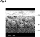
- FIG. 4 is an SEM image showing a cross section of a part of the phosphor panel 30.
- the phosphor panel 30 includes the above-described exit window 12, a phosphor layer 52 having a plurality of phosphor particles 51, a metal reflection film 53, and an oxide film 54.
- the phosphor surface 5 includes a phosphor layer 52, a metal reflection film 53, and an oxide film 54 covering the phosphor layer 52 and the metal reflection film 53.
- the exit window 12 functions as a light transmissive substrate that transmits the fluorescence L2.
- the phosphor layer 52 is provided on the exit window 12 (the inner surface 12a which is the vacuum-side surface of the exit window 12).
- the phosphor layer 52 is formed on the exit window 12 by, for example, a manufacturing method (precipitation method or the like) described later.
- the thickness t1 of the phosphor layer 52 is, for example, about 4 ⁇ m to 8 ⁇ m.
- the phosphor layer 52 is configured as an aggregate of a plurality of phosphor particles 51.
- the particle diameter of the phosphor particle 51 is, for example, about 1 ⁇ m to 4 ⁇ m.
- the center value of the particle size distribution of the phosphor particles 51 is about 2 ⁇ m.
- the phosphor particles 51 have a property of emitting fluorescence corresponding to the incident photoelectrons.
- the phosphor particle 51 is, for example, gadolinium oxysulfide (GOS).
- the phosphor layer 52 includes a binder for binding (adhering) the plurality of phosphor particles 51 to each other.
- the binder C made of potassium silicate adheres to the surface of the phosphor particle 51. Adjacent phosphor particles 51 are bonded to each other via the binder C.
- the metal reflection film 53 is provided on the phosphor layer 52 (on the side opposite to the exit window 12 side of the phosphor layer 52).
- the metal reflection film 53 is a so-called metal back, and has a relatively high reflectance with respect to the light passing through the microchannel plate 4 and a relatively high transmittance with respect to the photoelectron E2 from the microchannel plate 4.
- the metal reflection film 53 is formed of, for example, an aluminum film.
- the thickness t2 of the metal reflection film 53 is, for example, about 50 nm to 120 nm.
- the metal reflection film 53 has a function of preventing charge-up of the phosphor layer 52, a function of reflecting fluorescence from the phosphor particles 51 toward the exit window 12, and the like.
- the metal reflection film 53 is formed on the phosphor layer 52 by performing a process of removing an organic film after performing vapor deposition or sputtering of a metal material (aluminum in the present embodiment) on the organic film provided on the phosphor layer 52.
- the metal reflection film 53 thus formed has openings 53a such as pinholes scattered therein.
- the oxide film 54 is formed so as to integrally cover the surface of the metal reflection film 53 and the surfaces of the phosphor particles 51.
- the oxide film 54 is preferably formed of a material having a relatively high electron transmittance so as not to inhibit electrons from entering the phosphor particles 51. From such a viewpoint, the oxide film 54 is preferably formed of an element having a relatively small atom number.
- the oxide film 54 is formed by performing film formation by atomic layer deposition (ALD) on a formed body in which the exit window 12, the phosphor layer 52, and the metal reflection film 53 are formed in a layered manner as described above. Since film formation by ALD is a technique based on the principle of gas adsorption, film formation can also be performed inside the formed body by allowing gas to enter the inside of the formed body from a gap of the formed body (for example, the opening 53a of the metal reflection film 53, the gap between the phosphor layer 52 and the inner surface 12a of the exit window 12, the gap between the phosphor layer 52 and the inner surface53c of the metal reflection film 53, etc.). In addition, according to ALD, a dense continuous film without gaps can be formed even on a fine uneven surface.
- ALD atomic layer deposition
- the oxide film 54 is formed not only on the outer surface of the formed body (the outer surface 53b of the metal reflection film 53 and the outer surface 12b of the exit window 12) but also inside the formed body (the surface of the opening 53a and the inner surface53c of the metal reflection film 53, the inner surface 12a of the exit window 12, and the surfaces of the phosphor particles 51).
- the oxide film 54 is integrally (continuously) formed on the outer surface and inside of the formed body.
- the oxide film 54 covers the surface of the phosphor particle 51 so as to contain the binder C adhered to the surface of the phosphor particle 51.
- the thickness of the oxide film 54 is, for example, about 3 nm to 12 nm.
- the material of the oxide film 54 is preferably an oxide of Be, Mg, Al, Si, Ca, Ti, Cr, Mn, Fe, Co, Ni, Cu, Zn, Ga, Ge, Sr, Y, Sn, Ba, Hf, Ta, W, Ir, or the like.
- the oxide film 54 is preferably an aluminum oxide film (Al 2 O 3 ), a titanium oxide film (TiO 2 ), a zinc oxide film (ZnO), or a silicon oxide film (SiO 2 ). With such a material, film formation by ALD can be relatively easily performed, and a dense and continuous film can be favorably formed.
- the oxide film 54 is an aluminum oxide film having a thickness of 5 nm formed by ALD.
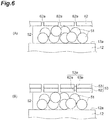
- FIG. 5 and FIG. 6 are schematic views showing the manufacturing process of the phosphor panel 30.
- a fluorophore solution is prepared. First, a plurality of phosphor particles 51 are mixed with pure water and filtered potassium silicate. The solution thus obtained is then subjected to ultrasonic agitation. As a result, a solution in which the plurality of phosphor particles 51 are uniformly dispersed is obtained. Subsequently, the solution is further stirred with further addition of barium acetate.
- a mounting member 24 (metal flange, see FIGS. 1 and 2 ) is provided so as to surround the exit window 12 when viewed from the light emission direction of the exit window 12 (the direction orthogonal to the inner surface 12a).
- a cylinder (not shown) is fixed to the mounting member 24.
- the cylinder is arranged such that the inner surface 12a of the exit window 12 is located inside the cylinder. That is, the cylinder is fixed to the mounting member 24 such that the portion where the phosphor surface 5 is to be formed (i.e., the inner surface 12a of the exit window 12) is located inside the cylinder.
- the exit window 12 and the mounting member 24 are fixed to each other through the frit glass 29 (see FIG. 2 ).
- the fluorescence substance solution prepared in the preparation step is placed in the cylinder fixed to the inner surface 12a as described above.
- the phosphor particles 51 contained in the fluorescence substance solution contained in the cylinder are allowed to stand for a certain period of time, and thereby settle on the inner surface 12a. Thereafter, the supernatant liquid in the cylinder and the moisture adhering to the surface of the phosphor particle 51 are carefully sucked. As a result, as shown in (A) of FIG. 5 , a phosphor layer 52 having a plurality of phosphor particles 51 is formed on the inner surface 12a of the exit window 12.
- an organic film 61 is formed on the phosphor layer 52 (opposite to the exit window 12).
- the organic film 61 is a nitrocellulose film.
- the organic film 61 is provided substantially flat on the phosphor layer 52. That is, the organic film 61 is not provided along the surface shape of the phosphor particles 51, but is placed above the plurality of phosphor particles 51 while maintaining a substantially flat shape.
- a metal reflection film 62 (first metal reflection film) is formed on the organic film 61.
- the metal reflection film 62 is an aluminum film.
- the thickness of the metal reflection film 62 is, for example, about 10 nm to 20 nm.
- the metal reflection film 62 is provided on the organic film 61 by vapor deposition or sputtering. As described above, since the organic film 61 is provided substantially flat on the phosphor layer 52, the metal reflection film 62 can be formed substantially flat along the shape of the organic film 61.
- the formed body including the exit window 12, the phosphor layer 52, the organic film 61, and the metal reflection film 62 as shown in (C) of FIG. 5 is fired.
- the formed body is fired, for example, in the atmosphere at 350 degrees Celsius.
- the organic film 61 is burned and removed.
- the metal reflection film 62 is disposed on the phosphor layer 52. Note that openings 62a such as pinholes are scattered in the metal reflection film 62 formed by vapor deposition or sputtering.
- a metal reflection film 63 (second metal reflection film) is formed on the metal reflection film 62 located on the phosphor layer 52.
- a part of the metal reflection film 62 may be changed into a metal oxide film (alumina in the present embodiment) or damaged by firing for removing the organic film 61.
- a metal reflection film here, an aluminum film
- a metal reflection film 63 is formed on the metal reflection film 62 in order to secure a metal reflection film having a sufficient layer thickness.
- the metal reflection film 53 includes the metal reflection film 62 and the metal reflection film 63.
- the metal reflection film 63 may be formed of the same material as the metal reflection film 62 or may be formed of a metal material different from the metal reflection film 62. In the present embodiment, as an example, the metal reflection film 63 is formed of the same aluminum as the metal reflection film 62. The metal reflection film 63 is formed on the metal reflection film 62 by vapor deposition or sputtering. The thickness of the metal reflection film 63 is, for example, about 40 nm to 100 nm. An opening 63a communicating with the opening 62a is formed in a portion of the metal reflection film 63 corresponding to the opening 62a of the metal reflection film 62. The opening 53a of the metal reflection film 53 is composed of an opening 62a and an opening 63a.
- an oxide film 54 (see FIG. 3 ) is formed by atomic layer deposition (ALD) to integrally cover the surface of the metal reflection film 53 (metal reflection film 62 and metal reflection film 63) and the surfaces of the phosphor particles 51.
- ALD atomic layer deposition
- film formation by ALD is performed on the entire formed body (exit window 12, phosphor layer 52, and metal reflection film 53) in the state shown in (B) of FIG. 6 .
- the oxide film 54 is formed on the outer surface of the formed body (the outer surface 53b of the metal reflection film 53 and the outer surface 12b of the exit window 12) and the inside of the formed body (the surface of the opening 53a and the inner surface53c of the metal reflection film 53, the inner surface 12a of the exit window 12, and the surfaces of the phosphor particles 51).
- the metal reflection film 53 and the oxide film 54 formed by ALD may have a structure in which a metal oxide film generated by baking is formed outside an aluminum film and an oxide film 54 formed by ALD is further formed outside the metal oxide film.
- the oxide film 54 is formed so as to integrally cover the surfaces (the outer surface 53b and the inner surface53c) of the metal reflection film 53 and the surfaces of the phosphor particles 51. Since the surface of the metal reflection film 53 is protected by the oxide film 54, the strength of the metal reflection film 53 is improved. Furthermore, since the adhesion between the metal reflection film 53 and the phosphor layer 52 (phosphor particles 51) is improved via the oxide film 54, the metal reflection film 53 is less likely to be peeled off from the phosphor layer 52. Therefore, according to the phosphor panel 30, peeling of the metal reflection film 53 can be effectively suppressed.
- the metal reflection film 53 is an aluminum film. Accordingly, the function as the metal back described above (that is, the function of preventing charge-up of the phosphor layer 52, the function of reflecting the fluorescence L2 from the phosphor particle 51, and the like) can be suitably exhibited.
- the oxide film 54 is formed of an aluminum oxide film. Accordingly, the strength of the metal reflection film 53 and the adhesion between the metal reflection film 53 and the phosphor layer 52 can be suitably improved.
- the oxide film 54 is formed of a titanium oxide film, a zinc oxide film, or a silicon oxide film, the same effect as described above is obtained.
- the phosphor particle 51 is gadolinium oxysulfide.
- the phosphor layer 52 of the phosphor panel 30 used as an electron detector in an image intensifier or the like can be suitably formed.
- the phosphor layer 52 includes a binder C that binds the plurality of phosphor particles 51 to each other. Thus, the phosphor particles 51 are fixed to each other, and the structure of the phosphor layer 52 can be stabilized.
- binder C is potassium silicate. Accordingly, the phosphor particles 51 can be suitably bonded to each other.
- the exit window 12 is a fiber optic plate (FOP) formed by bundling a plurality of optical fibers.
- FOP fiber optic plate
- the image intensifier 1 includes a photocathode 3 that emits a photoelectron E1 in response to incident light L1, a microchannel plate 4 that multiplies the photoelectron E1 emitted from the photocathode 3, and a phosphor panel 30.
- the phosphor panel 30 is disposed such that the phosphor layer 52 receives the photoelectron E2 multiplied by the microchannel plate 4 and emits fluorescence L2 corresponding to the photoelectron E2. That is, as shown in FIG. 2 , phosphor surface 5 is arranged to face microchannel plate 4.
- the metal reflection film 53 of the phosphor panel 30 is more difficult to peel off than in the related art, it is possible to improve handleability of the phosphor panel 30 at the time of manufacturing a product. That is, the phosphor panel 30 can be handled more easily than in the related art.
- the metal reflection film 53 is prevented from peeling off from the phosphor panel 30, it is possible to prevent the quality of the image intensifier 1 from deteriorating due to the peeling off of the metal reflection film 53.
- an image intensifier it is known that peeling of a metal reflection film (metal back) may cause deterioration in image quality of an image obtained by the image intensifier. Therefore, according to the above-described image intensifier 1, it is possible to suppress a decrease in image quality due to peeling of the metal reflection film 53.
- the phosphor particles 51 are covered with the oxide film 54, absorption of gas to the phosphor particles 51 (or the binder C adhered to the phosphor particles 51) is suppressed, and emission of gas from the phosphor particles 51 during the operation of the image intensifier 1 is suppressed. Accordingly, it is possible to suppress a phenomenon (ion feedback) in which the gas emitted from the phosphor particle 51 is ionized and reaches the photocathode 3, and to suppress deterioration of the photocathode 3 (deterioration of cathode sensitivity) due to the phenomenon. As a result, the life characteristic (product life) of the image intensifier 1 can be improved.
- potassium silicate used as the binder C has a property of relatively easily adsorbing gas. Therefore, when potassium silicate is used as the binder C as in the present embodiment, it can be said that the above-described effect obtained by covering the phosphor particles 51 with the oxide film 54 is particularly large.
- FIG. 7 is a diagram showing light irradiation conditions in the life test (MTTF test).
- a of FIG. 8 shows a test result of an image intensifier according to a comparative example (hereinafter simply referred to as "comparative example”).
- B) of FIG. 8 shows a test result of an image intensifier according to an example (hereinafter, simply referred to as "example”).
- the example is an image intensifier having the same configuration as the image intensifier 1 described above.
- the example includes the above-described phosphor panel 30 as the phosphor panel.
- the comparative example is an image intensifier including a phosphor panel in which the formation of the oxide film 54 by ALD is omitted.
- the example is an image intensifier obtained as follows. That is, in the manufacturing process of the example, the phosphor panel in the state (that is, the state shown in (B) of FIG. 6 ) before the film formation by ALD described above is performed was subjected to a firing (baking) process of heating at 350 degrees Celsius for 8 hours in a vacuum. Thereafter, the oxide film 54 was formed on the phosphor panel by ALD. Thereafter, the phosphor panel 30 thus obtained was sealed in a housing 2 together with a photocathode 3 and a microchannel plate 4 to obtain the example. On the other hand, in the manufacturing process of the comparative example, the phosphor panel in the state shown in (B) of FIG.
- each of the above-described example and comparative example was repeatedly irradiated with light under the light irradiation conditions shown in FIG. 7 . That is, as shown in FIG. 7 , each of the example and the comparative example was intermittently irradiated with light whose light intensity regularly changed in the range of 0.00054 lux to 54 lux within 12 minutes.
- Sk and LG decrease to about 10% at the time when about 300 hours have elapsed from the start of the life test (light irradiation).
- (B) of FIG. 8 in the example, Sk and LG are maintained in a state of 40% or more even at the time when 1000 hours have elapsed from the start of the life test. That is, in the comparative example, LG is decreased due to the decrease in Sk.
- the state in which LG is relatively high can be maintained even after a long time has elapsed.
- the above-described oxide film 54 is formed so as to include the phosphor particles 51 and the binder C, and thus the gas release from the phosphor particles 51 and the binder C is suppressed.
- the above-described ion feedback was suppressed and the deterioration of Sk was suppressed.
- the method of manufacturing the phosphor panel 30 according to the present embodiment includes: forming a phosphor layer 3 having a plurality of phosphor particles 51 on an exit window 12 (see (A) of FIG. 5 ); forming an organic film 61 on the phosphor layer 52 (see (B) of FIG. 5 ); forming a metal reflection film 62 (a portion of the metal reflection film 53) on the organic film 61 (see (C) of FIG. 5 ); removing the organic film 61 by firing (see (A) of FIG. 6 ); and forming an oxide film 54 integrally covering a surface of the metal reflection film 53 and surfaces of the phosphor particles 51 by ALD.
- the metal reflection film 62 is formed on the organic film 61 formed on the phosphor layer 52. Accordingly, the metal molecules constituting the metal reflection film 62 are prevented from being mixed into the phosphor layer 52, and the metal reflection film 53 can be appropriately provided on the phosphor layer 52.
- the oxide film 54 is formed by ALD so as to integrally cover the surface of the metal reflection film 53 and the surfaces of the phosphor particles 51. As a result, as described above, the strength of the metal reflection film 53 is improved.
- the metal reflection film 53 is improved through the oxide film 54, the metal reflection film 53 is less likely to be peeled off from the phosphor layer 52. Therefore, according to the above-described manufacturing method, the phosphor panel 30 in which peeling of the metal reflection film 53 is effectively suppressed can be manufactured.
- the above-described effect of the present embodiment cannot be obtained only by continuously coating the surfaces of a plurality of phosphor particles. That is, in the above-described manufacturing method, the oxide film 54 is continuously formed over the metal reflection film 53 and the phosphor layer 52 by performing film formation by ALD in a state where the metal reflection film 53 is formed on the phosphor layer 52. As a result, the adhesion between the metal reflection film 53 and the phosphor layer 52 can be improved, and damage such as peeling of the metal reflection film 53 can be effectively suppressed.
- the organic film 61 is a nitrocellulose film. Accordingly, the organic film 61 suitable for forming the metal reflection film 53 can be suitably formed.
- the metal reflection film 53 is formed by vapor deposition or sputtering. Accordingly, the metal reflection film 53 can be suitably formed on the organic film 61. Further, the metal reflection film 53 in which the opening 53a (pinhole) is appropriately provided is formed by vapor deposition or sputtering. Accordingly, in the film formation of the oxide film 54 by ALD, the gas for forming the oxide film 54 can be suitably introduced into the phosphor layer 52 through the opening 53a of the metal reflection film 53. As a result, the oxide film 54 can be suitably formed.
- the method further includes forming a metal reflection film 63 on the metal reflection film 62 which is the metal reflection film located on the phosphor layer 52 after the organic film 61 is removed (see (B) of FIG. 6 ).
- the oxide film 54 is formed to cover the metal reflection film 53 (i.e., the metal reflection film 62 and the metal reflection film 63) and the phosphor particles 51.
- a part of the metal reflection film 62 initially formed on the organic film 61 may be changed into a metal oxide film (alumina in this embodiment) or damaged by the firing step.
- the metal reflection film 62 initially formed on the organic film 61 may not sufficiently function as a metal reflection film for preventing charge-up of the phosphor layer 52.
- the function as the above-described metal reflection film can be ensured by the metal reflection film 62 and the metal reflection film 63.
- the thickness of the metal reflection film 62 (15 nm in this embodiment) is smaller than the thickness of the metal reflection film 63 (70 nm in this embodiment). In this manner, by forming the metal reflection film 62 formed on the organic film 61 to be relatively thin before the firing step, the organic film 61 can be suitably removed in the firing step. In addition, since the relatively thick metal reflection film 62 is formed after the organic film 61 is removed, the entire thickness of the metal reflection film (the thickness t2 of the metal reflection film 53) may be sufficiently secured.
- the phosphor panel 30 may be used in various optical devices in addition to the image intensifier.
- the phosphor panel 30 may be used as an electron detector in a scanning electron microscope.
- FIG. 9 is a schematic configuration diagram of a scanning electron microscope according to an embodiment.
- a scanning electron microscope 70 includes an electron gun 71 that generates an electron beam, an irradiation part 72 that irradiates a sample S with an electron beam B and scans the irradiation position of the electron beam on the sample S, and a phosphor panel 30.
- the phosphor panel 30 is disposed so that the phosphor layer 52 receives the photoelectron E generated in the sample S in response to the irradiation of the electron beam to the sample S and emits fluorescence corresponding to the photoelectron E. That is, as shown in FIG. 9 , phosphor surface 5 is arranged to face sample S.
- the metal reflection film 53 of the phosphor panel 30 is less likely to be peeled off than in the related art, and thus it is possible to improve handleability of the phosphor panel 30 at the time of manufacturing a product. That is, the phosphor panel 30 can be handled more easily than in the related art.
- the scanning electron microscope 70 is a so-called transmission type scanning electron microscope in which the incident surface of the electron beam B and the emission surface of the photoelectron E in the sample S are positioned on opposite sides
- the phosphor panel 30 may be used as an electron detection unit of a so-called reflection type scanning electron microscope in which the incident surface of the electron beam and the emission surface of the photoelectron in the sample are the same.
- the present disclosure is not limited to the above-described embodiment.
- the material and shape of each component are not limited to those described above, and various materials and shapes can be adopted.
- the exit window 12 may be formed by a glass substrate instead of the FOP.
- the following film forming process may be additionally performed in order to enhance the ion feedback suppression effect described above. That is, after the phosphor layer 52 is formed on the exit window 12 (the state shown in (A) of FIG. 5 ), an oxide film (for example, aluminum oxide) integrally covering the surface of the phosphor layer 52 (that is, the surface of each phosphor particle 51) may be formed by ALD. Alternatively, an oxide film may be formed on the surface of each phosphor particle 51 before preparing the fluorescence solution. That is, the phosphor solution may be prepared using the phosphor particles 51 on which an oxide film is formed in advance.
- an oxide film for example, aluminum oxide
- an oxide film may be formed on the surface of each phosphor particle 51 before preparing the fluorescence solution. That is, the phosphor solution may be prepared using the phosphor particles 51 on which an oxide film is formed in advance.
- the phosphor particles 51 can be covered with the oxide film as early as possible in the manufacturing process of the phosphor panel 30, so that the adsorption of the gas to the phosphor particles 51 can be effectively suppressed.
- the binder C potassium silicate in the above embodiment may be omitted. That is, in the state shown in (A) of FIG. 5 , the step of immersing the surface of each phosphor particle 51 in potassium silicate may be omitted.
- the metal reflection film 63 is formed on the metal reflection film 62 in the above embodiment (see (B) of FIG. 6 ), the formation of the metal reflection film 63 may be omitted if the metal reflection film 62 after the organic film 61 is removed can sufficiently exhibit the function as the metal back described above.
- the metal reflection film 53 in the above embodiment is constituted only by the metal reflection film 62.
Landscapes
- Chemical & Material Sciences (AREA)
- Analytical Chemistry (AREA)
- Engineering & Computer Science (AREA)
- Materials Engineering (AREA)
- Organic Chemistry (AREA)
- Manufacturing & Machinery (AREA)
- Measurement Of Radiation (AREA)
- Image-Pickup Tubes, Image-Amplification Tubes, And Storage Tubes (AREA)
- Cathode-Ray Tubes And Fluorescent Screens For Display (AREA)
- Formation Of Various Coating Films On Cathode Ray Tubes And Lamps (AREA)
Abstract
Description
- The present disclosure relates to a method of manufacturing a phosphor panel, a phosphor panel, an image intensifier, and a scanning electron microscope.
- In the related art, for example, in an image intensifier, a scanning electron microscope, and the like, a phosphor panel is used as an electron detection unit that detects photoelectrons. For example,
Patent Document 1 discloses that a phosphor layer (fluorescence film) is formed
of a particulate fluorescence substance, and a metal reflection film (aluminum layer) is provided on an electron incident surface side of the phosphor layer to prevent charge-up of the phosphor layer.Patent Document 1 discloses a method of forming a metal reflection film on a nitrocellulose film after forming the nitrocellulose film on the phosphor layer, then forming the metal reflection film on the phosphor layer by removing the nitrocellulose film. - [Patent Document 1]
Japanese Unexamined Patent Publication No. H1-243345 - In the method of forming the metal reflection film described above, since the nitrocellulose film is interposed between the phosphor layer and the metal reflection film, the metal reflection film is not directly formed on the phosphor layer. Therefore, the metal reflection film is not sufficiently adhered to the phosphor layer, and is relatively easily peeled off from the phosphor layer. In addition, the peeling of the metal reflection film may cause deterioration in quality of a product including the phosphor panel as an electron detector. For example, in an image intensifier, the peeling of the metal reflection film may cause deterioration in image quality.
- Therefore, it is an object of the present disclosure to provide a method of manufacturing a phosphor panel, a phosphor panel, an image intensifier, and a scanning electron microscope, which can effectively suppress peeling of a metal reflection film.
- According to an aspect of the present disclosure, a method of manufacturing a phosphor panel includes: forming a phosphor layer having a plurality of phosphor particles on a light transmissive substrate; forming an organic film on the phosphor layer; forming a metal reflection film on the organic film; removing the organic film by firing; and forming an oxide film integrally covering a surface of the metal reflection film and surfaces of the phosphor particles by atomic layer deposition.
- In the method of manufacturing the phosphor panel, the metal reflection film is formed on the organic film formed on the phosphor layer. Accordingly, the metal molecules constituting the metal reflection film are prevented from being mixed into the phosphor layer, and the metal reflection film can be appropriately provided on the phosphor layer. After the organic film is removed by firing, an oxide film is formed by atomic layer deposition to integrally cover the surface of the metal reflection film and the surfaces of the phosphor particles. Since the surface of the metal reflection film is protected by the oxide film, the strength of the metal reflection film is improved. In addition, since the adhesion between the metal reflection film and the phosphor layer (phosphor particle) is improved through the oxide film, the metal reflection film is not easily separated from the phosphor layer. Therefore, according to the above manufacturing method, it is possible to manufacture a phosphor panel in which peeling of the metal reflection film is effectively suppressed.
- The organic film may be a nitrocellulose film. Accordingly, an organic film suitable for forming a metal reflection film can be suitably formed.
- The metal reflection film may be formed by vapor deposition or sputtering. Thus, the metal reflection film can be suitably formed on the organic film. In addition, a metal reflection film having an appropriate opening (pinhole) is formed by vapor deposition or sputtering. Accordingly, in the formation of the oxide film by the atomic layer deposition method, the gas for forming the oxide film can enter the phosphor layer through the opening of the metal reflection film. As a result, the oxide film can be suitably formed.
- The manufacturing method may further include forming a second metal reflection film on a first metal reflection film which is the metal reflection film located on the phosphor layer after the organic film is removed, and in the forming the oxide film, the oxide film may be formed to cover the first metal reflection film, the second metal reflection film, and the phosphor particles. In the above manufacturing methods, a part of a metal reflection film (first metal reflection film) initially formed on the organic film may be changed into a metal oxide film or damaged by the firing process. As a result, the first metal reflection film alone may not sufficiently exhibit a function as a metal reflection film such as prevention of charge-up of the phosphor layer. On the other hand, in the above-described manufacturing method, the above-described function as the metal reflection film can be ensured by the first metal reflection film and the second metal reflection film.
- A phosphor panel according to an aspect of the present disclosure includes a light transmissive substrate, a phosphor layer disposed on the light transmissive substrate and having a plurality of phosphor particles, a metal reflection film disposed on the phosphor layer, and an oxide film integrally covering a surface of the metal reflection film and surfaces of the phosphor particles.
- In the phosphor panel, the oxide film is formed to integrally cover the surface of the metal reflection film and the surfaces of the phosphor particle. Since the surface of the metal reflection film is protected by the oxide film, the strength of the metal reflection film is improved. In addition, since the adhesion between the metal reflection film and the phosphor layer (phosphor particle) is improved through the oxide film, the metal reflection film is not easily separated from the phosphor layer. Therefore, according to the phosphor panel, peeling of the metal reflection film can be effectively suppressed.
- The metal reflection film may be an aluminum film. Accordingly, the function as the metal reflection film described above can be suitably exhibited.
- The oxide film may be an aluminum oxide film, a titanium oxide film, a zinc oxide film, or a silicon oxide film. Accordingly, the strength of the metal reflection film and the adhesion between the metal reflection film and the phosphor layer can be suitably improved.
- The phosphor particle may be gadolinium oxysulfide. Accordingly, the phosphor layer of a phosphor panel used as an electron detector in an image intensifier or the like can be suitably formed.
- The phosphor layer may include a binder that binds a plurality of phosphor particles to each other. Thus, the phosphor particles are fixed to each other, and the structure of the phosphor layer can be stabilized.
- The binder may be potassium silicate. Accordingly, the phosphor particles can be suitably bonded to each other.
- The light transmissive substrate may be a fiber optic plate formed by bundling a plurality of optical fibers. This makes it possible to transmit fluorescence emitted from the phosphor layer to the outside with high efficiency and low distortion.
- An image intensifier according to an aspect of the present disclosure includes a photocathode configured to emit photoelectrons in response to incident light, an electron multiplier configured to multiply the photoelectron emitted from the photocathode, and the phosphor panel disposed so that the phosphor layer receives the photoelectron multiplied by the electron multiplier and emits fluorescence corresponding to the photoelectron.
- A scanning electron microscope according to an aspect of the present disclosure includes: an electron gun configured to generate an electron beam; an irradiation part configured to irradiate a sample with the electron beam and scan an irradiation position of the electron beam on the sample; and the phosphor panel disposed so that the phosphor layer receives a photoelectron generated in the sample in response to the irradiation of the sample with the electron beam and emits fluorescence corresponding to the photoelectron.
- The image intensifier or the scanning electron microscope includes the above-described phosphor panel as an electron detector. As described above, since the metal reflection film is more difficult to peel off from the phosphor panel than in the related art, it is possible to improve handleability of the phosphor panel at the time of manufacturing a product. That is, the phosphor panel can be handled more easily than in the prior art. In addition, since peeling of the metal reflection film is suppressed in the phosphor panel, it is possible to suppress deterioration in quality of a product due to peeling of the metal reflection film. For example, in an image intensifier, it is possible to suppress deterioration in image quality due to peeling of a metal reflection film. In addition, since the phosphor particles are covered with the oxide film, absorption of gas to the phosphor particles (or the binder attached to the phosphor particles) is suppressed, and emission of gas from the phosphor particles during operation of the image intensifier is suppressed. As a result, it is possible to suppress a phenomenon (ion feedback) in which the gas emitted from the phosphor particles is ionized and reaches the photocathode, and to suppress deterioration of the photocathode (deterioration of cathode sensitivity) due to the phenomenon. As a result, the life characteristics (product life) of the image intensifier can be improved.
- According to the present disclosure, it is possible to provide a method of manufacturing a phosphor panel, a phosphor panel, an image intensifier, and a scanning electron microscope that can effectively suppress peeling of a metal reflection film.
-
-
FIG. 1 is a partial cross-sectional view of an image intensifier including a phosphor panel according to an embodiment. -
FIG. 2 is an enlarged cross-sectional view of a main part of the image intensifier shown inFIG. 1 . -
FIG. 3 is a schematic cross-sectional view showing a main part of the phosphor panel. -
FIG. 4 shows an SEM image of a phosphor panel. -
FIG. 5 is a view showing a manufacturing process of a phosphor panel. -
FIG. 6 is a view showing a manufacturing process of a phosphor panel. -
FIG. 7 is a diagram showing light irradiation conditions in the life test (MTTF test).- (A) of
FIG. 8 shows a test result of an image intensifier according to a comparative example. - (B) of
FIG. 8 shows a test result of the image intensifier according to an example.
- (A) of
-
FIG. 9 is a schematic configuration diagram of a scanning electron microscope including a phosphor panel according to an embodiment. - Hereinafter, embodiments of the present disclosure will be described with reference to the drawings. In the drawings, the same or corresponding portions are denoted by the same reference numerals, and redundant description is omitted. In the drawings, some of the characteristic portions according to the embodiments are exaggerated for easy understanding, and the dimensions may be different from the actual dimensions. In the following description, terms such as "upper" and "lower" are used for convenience based on the state shown in the drawings.
-
FIGS. 1 and2 illustrate an image intensifier including a phosphor panel according to an embodiment. Theimage intensifier 1 of this embodiment includes ahousing 2. Theimage intensifier 1 includes aphotocathode 3, a microchannel plate 4 (electron multiplier), and aphosphor surface 5 inside thehousing 2. - The inside of the
image intensifier 1 is maintained in a high vacuum state by hermetically sealing both ends of a substantially hollowcylindrical housing 2 with a substantially disk-shapedentrance window 11 and exit window 12 (light transmissive substrates). Thehousing 2 includes, for example, aside tube 13 made of ceramic having a substantially hollow cylindrical shape, amold member 14 made of silicone rubber having a substantially hollow cylindrical shape and covering a side portion of theside tube 13, and acase member 15 made of polyoxymethylene having a substantially hollow cylindrical shape and covering a side portion and a bottom portion of themold member 14. - For example, two through holes are formed at both ends of the
mold member 14. One end of thecase member 15 is opened, and the other end of thecase member 15 is formed with a through-hole whose periphery is aligned with one through-hole of themold member 14. On one end side of themold member 14, anentrance window 11 made of glass is joined to a surface around one through hole of themold member 14. A thin-film photocathode 3 is provided substantially at the center of the vacuum-side surface of theentrance window 11. Theentrance window 11 is a plate-shaped member made of, for example, quartz glass. Aphotocathode 3 is formed on the plate-shaped member. Thephotocathode 3 is formed of, for example, a compound of antimony and an alkali, a semiconductor crystal having a surface on which an alkali molecule such as Cs is adsorbed, or the like. - On the other hand, on the other end side of the
mold member 14, anexit window 12 is fitted into the other through hole of themold member 14. A thin-film phosphor surface 5 is provided at a substantially central portion of the vacuum-side surface of theexit window 12. Theexit window 12 is, for example, a fiber optic plate (FOP) configured by bundling a plurality of optical fibers. The optical axes of the respective optical fibers of theexit window 12 are orthogonal to thephotocathode 3, and the vacuum-side end surfaces thereof are flush with each other. Aphosphor surface 5 is provided on the vacuum-side surface of theexit window 12. Theexit window 12 and thephosphor surface 5 constitute aphosphor panel 30. - A substantially disk-shaped
microchannel plate 4 is disposed between thephotocathode 3 and thephosphor surface 5. Themicrochannel plate 4 is supported by an inner edge of a mountingmembers side tube 13, and faces thephotocathode 3 and thephosphor surface 5 with a predetermined gap therebetween. Themicrochannel plate 4 functions as an electron multiplier that multiplies photoelectrons emitted from thephotocathode 3. Specifically,microchannel plate 4 multiplies photoelectrons emitted fromphotocathode 3 and outputs the multiplied photoelectrons towardphosphor surface 5. - In the peripheral region of the vacuum-side surface of the
entrance window 11, a metal electrode layer (not shown) is electrically connected to thephotocathode 3. In order to connect the electrode layer to thephotocathode 3, a mountingmember 23 held between aside tube 13 and anentrance window 11 is extended into themold member 14 and fixed. In the peripheral region of the vacuum-side surface of theexit window 12, another electrode layer (not shown) made of metal is electrically connected to thephosphor surface 5. In order to connect the other electrode layer to thephosphor surface 5, a mountingmember 24 held between theside tube 13 and themold member 14 is extended into themold member 14 and fixed. - One end of each of
lead wires 25 to 28 made of, for example, kovar metal is connected to an end of each of the mountingmembers 21 to 24. The other ends of thelead wires 25 to 28 airtightly penetrate themold member 14 and thecase member 15 to protrude to the outside, and are electrically connected to an external voltage source (not shown). Thus, a predetermined voltage from the external voltage source is applied to thephotocathode 3, themicrochannel plate 4, and thephosphor surface 5. A potential difference of, for example, about 200V is set between thephotocathode 3 and aninput surface 4a of themicrochannel plate 4. A potential difference of, for example, about 500V to 1200V is variably set between theinput surface 4a and anoutput surface 4b of themicrochannel plate 4. A potential difference of, for example, about 6 kV is set between theoutput surface 4b of themicrochannel plate 4 and thephosphor surface 5. - Next, the operation of the
image intensifier 1 will be described. When the incident light L1 is incident on thephotocathode 3 through theentrance window 11, thephotocathode 3 emits photoelectrons E1 in response to the incident light L1. When the photoelectrons E1 are incident on theinput surface 4a of themicrochannel plate 4, themicrochannel plate 4 multiplies the photoelectrons E1 and emits the multiplied photoelectrons E2 to thephosphor surface 5. When photoelectrons E2 are incident onphosphor surface 5,phosphor surface 5 emits fluorescence L2 corresponding to photoelectrons E2. The fluorescence L2 (light image) emitted from thephosphor surface 5 passes through theexit window 12 and is then acquired by an imaging unit such as a CCD camera. - Next, the structure of the
phosphor panel 30 will be described with reference toFIGS. 3 and4 .FIG. 3 is a schematic cross-sectional view showing a portion ofexit window 12 wherephosphor surface 5 is provided.FIG. 4 is an SEM image showing a cross section of a part of thephosphor panel 30. As shown inFIG. 3 , thephosphor panel 30 includes the above-describedexit window 12, aphosphor layer 52 having a plurality ofphosphor particles 51, ametal reflection film 53, and anoxide film 54. Thephosphor surface 5 includes aphosphor layer 52, ametal reflection film 53, and anoxide film 54 covering thephosphor layer 52 and themetal reflection film 53. Theexit window 12 functions as a light transmissive substrate that transmits the fluorescence L2. - The
phosphor layer 52 is provided on the exit window 12 (theinner surface 12a which is the vacuum-side surface of the exit window 12). Thephosphor layer 52 is formed on theexit window 12 by, for example, a manufacturing method (precipitation method or the like) described later. The thickness t1 of thephosphor layer 52 is, for example, about 4 µm to 8 µm. Thephosphor layer 52 is configured as an aggregate of a plurality ofphosphor particles 51. The particle diameter of thephosphor particle 51 is, for example, about 1 µm to 4 µm. The center value of the particle size distribution of thephosphor particles 51 is about 2 µm. Thephosphor particles 51 have a property of emitting fluorescence corresponding to the incident photoelectrons. Thephosphor particle 51 is, for example, gadolinium oxysulfide (GOS). Thephosphor layer 52 includes a binder for binding (adhering) the plurality ofphosphor particles 51 to each other. In the present embodiment, the binder C made of potassium silicate adheres to the surface of thephosphor particle 51.Adjacent phosphor particles 51 are bonded to each other via the binder C. - The
metal reflection film 53 is provided on the phosphor layer 52 (on the side opposite to theexit window 12 side of the phosphor layer 52). Themetal reflection film 53 is a so-called metal back, and has a relatively high reflectance with respect to the light passing through themicrochannel plate 4 and a relatively high transmittance with respect to the photoelectron E2 from themicrochannel plate 4. Themetal reflection film 53 is formed of, for example, an aluminum film. The thickness t2 of themetal reflection film 53 is, for example, about 50 nm to 120 nm. Themetal reflection film 53 has a function of preventing charge-up of thephosphor layer 52, a function of reflecting fluorescence from thephosphor particles 51 toward theexit window 12, and the like. As will be described in detail later, themetal reflection film 53 is formed on thephosphor layer 52 by performing a process of removing an organic film after performing vapor deposition or sputtering of a metal material (aluminum in the present embodiment) on the organic film provided on thephosphor layer 52. Themetal reflection film 53 thus formed hasopenings 53a such as pinholes scattered therein. - The
oxide film 54 is formed so as to integrally cover the surface of themetal reflection film 53 and the surfaces of thephosphor particles 51. Theoxide film 54 is preferably formed of a material having a relatively high electron transmittance so as not to inhibit electrons from entering thephosphor particles 51. From such a viewpoint, theoxide film 54 is preferably formed of an element having a relatively small atom number. - The
oxide film 54 is formed by performing film formation by atomic layer deposition (ALD) on a formed body in which theexit window 12, thephosphor layer 52, and themetal reflection film 53 are formed in a layered manner as described above. Since film formation by ALD is a technique based on the principle of gas adsorption, film formation can also be performed inside the formed body by allowing gas to enter the inside of the formed body from a gap of the formed body (for example, theopening 53a of themetal reflection film 53, the gap between thephosphor layer 52 and theinner surface 12a of theexit window 12, the gap between thephosphor layer 52 and the inner surface53c of themetal reflection film 53, etc.). In addition, according to ALD, a dense continuous film without gaps can be formed even on a fine uneven surface. - Accordingly, as shown in
FIG. 3 , theoxide film 54 is formed not only on the outer surface of the formed body (theouter surface 53b of themetal reflection film 53 and theouter surface 12b of the exit window 12) but also inside the formed body (the surface of theopening 53a and the inner surface53c of themetal reflection film 53, theinner surface 12a of theexit window 12, and the surfaces of the phosphor particles 51). Theoxide film 54 is integrally (continuously) formed on the outer surface and inside of the formed body. Theoxide film 54 covers the surface of thephosphor particle 51 so as to contain the binder C adhered to the surface of thephosphor particle 51. The thickness of theoxide film 54 is, for example, about 3 nm to 12 nm. - From the viewpoint of suitably performing film formation by ALD, the material of the
oxide film 54 is preferably an oxide of Be, Mg, Al, Si, Ca, Ti, Cr, Mn, Fe, Co, Ni, Cu, Zn, Ga, Ge, Sr, Y, Sn, Ba, Hf, Ta, W, Ir, or the like. Further, theoxide film 54 is preferably an aluminum oxide film (Al2O3), a titanium oxide film (TiO2), a zinc oxide film (ZnO), or a silicon oxide film (SiO2). With such a material, film formation by ALD can be relatively easily performed, and a dense and continuous film can be favorably formed. In the present embodiment, as an example, theoxide film 54 is an aluminum oxide film having a thickness of 5 nm formed by ALD. - Next, a method of manufacturing the
phosphor panel 30 will be described with reference toFIGS. 5 and6 .FIG. 5 andFIG. 6 are schematic views showing the manufacturing process of thephosphor panel 30. As a preparation step, a fluorophore solution is prepared. First, a plurality ofphosphor particles 51 are mixed with pure water and filtered potassium silicate. The solution thus obtained is then subjected to ultrasonic agitation. As a result, a solution in which the plurality ofphosphor particles 51 are uniformly dispersed is obtained. Subsequently, the solution is further stirred with further addition of barium acetate. - Subsequently, for example, a mounting member 24 (metal flange, see
FIGS. 1 and2 ) is provided so as to surround theexit window 12 when viewed from the light emission direction of the exit window 12 (the direction orthogonal to theinner surface 12a). A cylinder (not shown) is fixed to the mountingmember 24. The cylinder is arranged such that theinner surface 12a of theexit window 12 is located inside the cylinder. That is, the cylinder is fixed to the mountingmember 24 such that the portion where thephosphor surface 5 is to be formed (i.e., theinner surface 12a of the exit window 12) is located inside the cylinder. At this time, theexit window 12 and the mountingmember 24 are fixed to each other through the frit glass 29 (seeFIG. 2 ). - Subsequently, the fluorescence substance solution prepared in the preparation step is placed in the cylinder fixed to the
inner surface 12a as described above. Thephosphor particles 51 contained in the fluorescence substance solution contained in the cylinder are allowed to stand for a certain period of time, and thereby settle on theinner surface 12a. Thereafter, the supernatant liquid in the cylinder and the moisture adhering to the surface of thephosphor particle 51 are carefully sucked. As a result, as shown in (A) ofFIG. 5 , aphosphor layer 52 having a plurality ofphosphor particles 51 is formed on theinner surface 12a of theexit window 12. - Subsequently, after the
exit window 12 and thephosphor particles 51 are dried, the surface of eachphosphor particle 51 is immersed in potassium silicate. As a result, the binder C made of potassium silicate adheres to the surfaces of thephosphor particles 51, and thephosphor particles 51 are firmly bonded to each other via the binder C. As shown in (B) ofFIG. 5 , anorganic film 61 is formed on the phosphor layer 52 (opposite to the exit window 12). In the present embodiment, theorganic film 61 is a nitrocellulose film. Theorganic film 61 is provided substantially flat on thephosphor layer 52. That is, theorganic film 61 is not provided along the surface shape of thephosphor particles 51, but is placed above the plurality ofphosphor particles 51 while maintaining a substantially flat shape. - Subsequently, as shown in (C) of
FIG. 5 , a metal reflection film 62 (first metal reflection film) is formed on theorganic film 61. In the present embodiment, as an example, themetal reflection film 62 is an aluminum film. The thickness of themetal reflection film 62 is, for example, about 10 nm to 20 nm. Themetal reflection film 62 is provided on theorganic film 61 by vapor deposition or sputtering. As described above, since theorganic film 61 is provided substantially flat on thephosphor layer 52, themetal reflection film 62 can be formed substantially flat along the shape of theorganic film 61. - Subsequently, the formed body including the
exit window 12, thephosphor layer 52, theorganic film 61, and themetal reflection film 62 as shown in (C) ofFIG. 5 is fired. The formed body is fired, for example, in the atmosphere at 350 degrees Celsius. By firing, theorganic film 61 is burned and removed. As a result, as shown in (A) ofFIG. 6 , themetal reflection film 62 is disposed on thephosphor layer 52. Note thatopenings 62a such as pinholes are scattered in themetal reflection film 62 formed by vapor deposition or sputtering. - Subsequently, as shown in (B) of
FIG. 6 , after theorganic film 61 is removed, a metal reflection film 63 (second metal reflection film) is formed on themetal reflection film 62 located on thephosphor layer 52. This is because of the following reason. That is, a part of themetal reflection film 62 may be changed into a metal oxide film (alumina in the present embodiment) or damaged by firing for removing theorganic film 61. As a result, a metal reflection film (here, an aluminum film) having a sufficient layer thickness is not ensured, and themetal reflection film 62 alone may not sufficiently exhibit the function as the metal back described above. Therefore, ametal reflection film 63 is formed on themetal reflection film 62 in order to secure a metal reflection film having a sufficient layer thickness. Themetal reflection film 53 includes themetal reflection film 62 and themetal reflection film 63. - The
metal reflection film 63 may be formed of the same material as themetal reflection film 62 or may be formed of a metal material different from themetal reflection film 62. In the present embodiment, as an example, themetal reflection film 63 is formed of the same aluminum as themetal reflection film 62. Themetal reflection film 63 is formed on themetal reflection film 62 by vapor deposition or sputtering. The thickness of themetal reflection film 63 is, for example, about 40 nm to 100 nm. Anopening 63a communicating with theopening 62a is formed in a portion of themetal reflection film 63 corresponding to theopening 62a of themetal reflection film 62. Theopening 53a of themetal reflection film 53 is composed of anopening 62a and anopening 63a. - Subsequently, an oxide film 54 (see
FIG. 3 ) is formed by atomic layer deposition (ALD) to integrally cover the surface of the metal reflection film 53 (metal reflection film 62 and metal reflection film 63) and the surfaces of thephosphor particles 51. In the present embodiment, film formation by ALD is performed on the entire formed body (exit window 12,phosphor layer 52, and metal reflection film 53) in the state shown in (B) ofFIG. 6 . As a result, as shown inFIG. 3 , theoxide film 54 is formed on the outer surface of the formed body (theouter surface 53b of themetal reflection film 53 and theouter surface 12b of the exit window 12) and the inside of the formed body (the surface of theopening 53a and the inner surface53c of themetal reflection film 53, theinner surface 12a of theexit window 12, and the surfaces of the phosphor particles 51). - When the surface of the
metal reflection film 62 is changed to a metal oxide film in the firing (baking) process, themetal reflection film 53 and theoxide film 54 formed by ALD may have a structure in which a metal oxide film generated by baking is formed outside an aluminum film and anoxide film 54 formed by ALD is further formed outside the metal oxide film. - In the
phosphor panel 30 described above, theoxide film 54 is formed so as to integrally cover the surfaces (theouter surface 53b and the inner surface53c) of themetal reflection film 53 and the surfaces of thephosphor particles 51. Since the surface of themetal reflection film 53 is protected by theoxide film 54, the strength of themetal reflection film 53 is improved. Furthermore, since the adhesion between themetal reflection film 53 and the phosphor layer 52 (phosphor particles 51) is improved via theoxide film 54, themetal reflection film 53 is less likely to be peeled off from thephosphor layer 52. Therefore, according to thephosphor panel 30, peeling of themetal reflection film 53 can be effectively suppressed. - In this embodiment, the
metal reflection film 53 is an aluminum film. Accordingly, the function as the metal back described above (that is, the function of preventing charge-up of thephosphor layer 52, the function of reflecting the fluorescence L2 from thephosphor particle 51, and the like) can be suitably exhibited. - In the present embodiment, the
oxide film 54 is formed of an aluminum oxide film. Accordingly, the strength of themetal reflection film 53 and the adhesion between themetal reflection film 53 and thephosphor layer 52 can be suitably improved. When theoxide film 54 is formed of a titanium oxide film, a zinc oxide film, or a silicon oxide film, the same effect as described above is obtained. - In the present embodiment, the
phosphor particle 51 is gadolinium oxysulfide. Thus, thephosphor layer 52 of thephosphor panel 30 used as an electron detector in an image intensifier or the like can be suitably formed. - The
phosphor layer 52 includes a binder C that binds the plurality ofphosphor particles 51 to each other. Thus, thephosphor particles 51 are fixed to each other, and the structure of thephosphor layer 52 can be stabilized. - In this embodiment, binder C is potassium silicate. Accordingly, the
phosphor particles 51 can be suitably bonded to each other. - In the present embodiment, the
exit window 12 is a fiber optic plate (FOP) formed by bundling a plurality of optical fibers. Thus, the fluorescence L2 emitted from thephosphor layer 52 can be transmitted to the outside with high efficiency and low distortion. - The
image intensifier 1 includes aphotocathode 3 that emits a photoelectron E1 in response to incident light L1, amicrochannel plate 4 that multiplies the photoelectron E1 emitted from thephotocathode 3, and aphosphor panel 30. Thephosphor panel 30 is disposed such that thephosphor layer 52 receives the photoelectron E2 multiplied by themicrochannel plate 4 and emits fluorescence L2 corresponding to the photoelectron E2. That is, as shown inFIG. 2 ,phosphor surface 5 is arranged to facemicrochannel plate 4. In theimage intensifier 1, since themetal reflection film 53 of thephosphor panel 30 is more difficult to peel off than in the related art, it is possible to improve handleability of thephosphor panel 30 at the time of manufacturing a product. That is, thephosphor panel 30 can be handled more easily than in the related art. - In addition, since the
metal reflection film 53 is prevented from peeling off from thephosphor panel 30, it is possible to prevent the quality of theimage intensifier 1 from deteriorating due to the peeling off of themetal reflection film 53. Specifically, in an image intensifier, it is known that peeling of a metal reflection film (metal back) may cause deterioration in image quality of an image obtained by the image intensifier. Therefore, according to the above-describedimage intensifier 1, it is possible to suppress a decrease in image quality due to peeling of themetal reflection film 53. - Further, since the
phosphor particles 51 are covered with theoxide film 54, absorption of gas to the phosphor particles 51 (or the binder C adhered to the phosphor particles 51) is suppressed, and emission of gas from thephosphor particles 51 during the operation of theimage intensifier 1 is suppressed. Accordingly, it is possible to suppress a phenomenon (ion feedback) in which the gas emitted from thephosphor particle 51 is ionized and reaches thephotocathode 3, and to suppress deterioration of the photocathode 3 (deterioration of cathode sensitivity) due to the phenomenon. As a result, the life characteristic (product life) of theimage intensifier 1 can be improved. In particular, potassium silicate used as the binder C has a property of relatively easily adsorbing gas. Therefore, when potassium silicate is used as the binder C as in the present embodiment, it can be said that the above-described effect obtained by covering thephosphor particles 51 with theoxide film 54 is particularly large. - Referring to
FIGS. 7 and8 , the effect of improving the life characteristics in theimage intensifier 1 will be described in detail.FIG. 7 is a diagram showing light irradiation conditions in the life test (MTTF test). (A) ofFIG. 8 shows a test result of an image intensifier according to a comparative example (hereinafter simply referred to as "comparative example"). (B) ofFIG. 8 shows a test result of an image intensifier according to an example (hereinafter, simply referred to as "example"). Here, the example is an image intensifier having the same configuration as theimage intensifier 1 described above. Specifically, the example includes the above-describedphosphor panel 30 as the phosphor panel. On the other hand, the comparative example is an image intensifier including a phosphor panel in which the formation of theoxide film 54 by ALD is omitted. - More specifically, the example is an image intensifier obtained as follows. That is, in the manufacturing process of the example, the phosphor panel in the state (that is, the state shown in (B) of
FIG. 6 ) before the film formation by ALD described above is performed was subjected to a firing (baking) process of heating at 350 degrees Celsius for 8 hours in a vacuum. Thereafter, theoxide film 54 was formed on the phosphor panel by ALD. Thereafter, thephosphor panel 30 thus obtained was sealed in ahousing 2 together with aphotocathode 3 and amicrochannel plate 4 to obtain the example. On the other hand, in the manufacturing process of the comparative example, the phosphor panel in the state shown in (B) ofFIG. 6 was subjected to a firing (baking) process of heating at 350 degrees Celsius for 20 hours in vacuum. Thereafter, the phosphor panel immediately after the firing process was performed was sealed in a housing together with a photocathode and a microchannel plate to obtain the comparative example. - In the life test, the
entrance window 11 of each of the above-described example and comparative example was repeatedly irradiated with light under the light irradiation conditions shown inFIG. 7 . That is, as shown inFIG. 7 , each of the example and the comparative example was intermittently irradiated with light whose light intensity regularly changed in the range of 0.00054 lux to 54 lux within 12 minutes. - As a result, test results as shown in
FIG. 8 were obtained. InFIG. 8 , "Sk" is the emission sensitivity (cathode sensitivity) of the photocathode. "MCP gain" is the gain of the microchannel plate. "LG (Luminescence Gain)" is an indicator corresponding to the amount of fluorescence emitted from a phosphor layer. LG is a value obtained by the product of Sk, MCP gain, and luminance efficiency. The horizontal axis ofFIG. 8 indicates the elapsed time from the start of light irradiation. The vertical axis ofFIG. 8 indicates a state where the state at the start of the test is set as a reference (100%). As shown in (A) ofFIG. 8 , in the comparative example, Sk and LG decrease to about 10% at the time when about 300 hours have elapsed from the start of the life test (light irradiation). On the other hand, as shown in (B) ofFIG. 8 , in the example, Sk and LG are maintained in a state of 40% or more even at the time when 1000 hours have elapsed from the start of the life test. That is, in the comparative example, LG is decreased due to the decrease in Sk. On the other hand, in the example, since the deterioration rate of Sk is slower than that in the comparative example, the state in which LG is relatively high can be maintained even after a long time has elapsed. From the above, in the example, it is considered that the above-describedoxide film 54 is formed so as to include thephosphor particles 51 and the binder C, and thus the gas release from thephosphor particles 51 and the binder C is suppressed. As a result, in the example, it is considered that the above-described ion feedback was suppressed and the deterioration of Sk was suppressed. - The method of manufacturing the
phosphor panel 30 according to the present embodiment includes: forming aphosphor layer 3 having a plurality ofphosphor particles 51 on an exit window 12 (see (A) ofFIG. 5 ); forming anorganic film 61 on the phosphor layer 52 (see (B) ofFIG. 5 ); forming a metal reflection film 62 (a portion of the metal reflection film 53) on the organic film 61 (see (C) ofFIG. 5 ); removing theorganic film 61 by firing (see (A) ofFIG. 6 ); and forming anoxide film 54 integrally covering a surface of themetal reflection film 53 and surfaces of thephosphor particles 51 by ALD. - In the manufacturing method, the
metal reflection film 62 is formed on theorganic film 61 formed on thephosphor layer 52. Accordingly, the metal molecules constituting themetal reflection film 62 are prevented from being mixed into thephosphor layer 52, and themetal reflection film 53 can be appropriately provided on thephosphor layer 52. After theorganic film 61 is removed by firing, theoxide film 54 is formed by ALD so as to integrally cover the surface of themetal reflection film 53 and the surfaces of thephosphor particles 51. As a result, as described above, the strength of themetal reflection film 53 is improved. Furthermore, since the adhesion between themetal reflection film 53 and the phosphor layer 52 (phosphor particles 51) is improved through theoxide film 54, themetal reflection film 53 is less likely to be peeled off from thephosphor layer 52. Therefore, according to the above-described manufacturing method, thephosphor panel 30 in which peeling of themetal reflection film 53 is effectively suppressed can be manufactured. - To supplement the above effects, it is known to provide a coating layer of aluminum oxide or the like continuously coating the surfaces of a plurality of phosphor particles, as described in
Japanese Unexamined Patent Publication No. 2013-216800 oxide film 54 is continuously formed over themetal reflection film 53 and thephosphor layer 52 by performing film formation by ALD in a state where themetal reflection film 53 is formed on thephosphor layer 52. As a result, the adhesion between themetal reflection film 53 and thephosphor layer 52 can be improved, and damage such as peeling of themetal reflection film 53 can be effectively suppressed. - The
organic film 61 is a nitrocellulose film. Accordingly, theorganic film 61 suitable for forming themetal reflection film 53 can be suitably formed. Themetal reflection film 53 is formed by vapor deposition or sputtering. Accordingly, themetal reflection film 53 can be suitably formed on theorganic film 61. Further, themetal reflection film 53 in which theopening 53a (pinhole) is appropriately provided is formed by vapor deposition or sputtering. Accordingly, in the film formation of theoxide film 54 by ALD, the gas for forming theoxide film 54 can be suitably introduced into thephosphor layer 52 through theopening 53a of themetal reflection film 53. As a result, theoxide film 54 can be suitably formed. - The method further includes forming a
metal reflection film 63 on themetal reflection film 62 which is the metal reflection film located on thephosphor layer 52 after theorganic film 61 is removed (see (B) ofFIG. 6 ). In the process of forming theoxide film 54, theoxide film 54 is formed to cover the metal reflection film 53 (i.e., themetal reflection film 62 and the metal reflection film 63) and thephosphor particles 51. In the above-described manufacturing method, a part of themetal reflection film 62 initially formed on theorganic film 61 may be changed into a metal oxide film (alumina in this embodiment) or damaged by the firing step. As a result, themetal reflection film 62 initially formed on theorganic film 61 may not sufficiently function as a metal reflection film for preventing charge-up of thephosphor layer 52. On the other hand, according to the above-described manufacturing method, the function as the above-described metal reflection film can be ensured by themetal reflection film 62 and themetal reflection film 63. - The thickness of the metal reflection film 62 (15 nm in this embodiment) is smaller than the thickness of the metal reflection film 63 (70 nm in this embodiment). In this manner, by forming the
metal reflection film 62 formed on theorganic film 61 to be relatively thin before the firing step, theorganic film 61 can be suitably removed in the firing step. In addition, since the relatively thickmetal reflection film 62 is formed after theorganic film 61 is removed, the entire thickness of the metal reflection film (the thickness t2 of the metal reflection film 53) may be sufficiently secured. - The
phosphor panel 30 may be used in various optical devices in addition to the image intensifier. For example, thephosphor panel 30 may be used as an electron detector in a scanning electron microscope.FIG. 9 is a schematic configuration diagram of a scanning electron microscope according to an embodiment. As shown inFIG. 9 , ascanning electron microscope 70 according to this embodiment includes anelectron gun 71 that generates an electron beam, anirradiation part 72 that irradiates a sample S with an electron beam B and scans the irradiation position of the electron beam on the sample S, and aphosphor panel 30. Thephosphor panel 30 is disposed so that thephosphor layer 52 receives the photoelectron E generated in the sample S in response to the irradiation of the electron beam to the sample S and emits fluorescence corresponding to the photoelectron E. That is, as shown inFIG. 9 ,phosphor surface 5 is arranged to face sample S. In thescanning electron microscope 70, similarly to theimage intensifier 1 described above, themetal reflection film 53 of thephosphor panel 30 is less likely to be peeled off than in the related art, and thus it is possible to improve handleability of thephosphor panel 30 at the time of manufacturing a product. That is, thephosphor panel 30 can be handled more easily than in the related art. Although thescanning electron microscope 70 is a so-called transmission type scanning electron microscope in which the incident surface of the electron beam B and the emission surface of the photoelectron E in the sample S are positioned on opposite sides, thephosphor panel 30 may be used as an electron detection unit of a so-called reflection type scanning electron microscope in which the incident surface of the electron beam and the emission surface of the photoelectron in the sample are the same. - Although an embodiment of the present disclosure has been described above, the present disclosure is not limited to the above-described embodiment. For example, the material and shape of each component are not limited to those described above, and various materials and shapes can be adopted. For example, the
exit window 12 may be formed by a glass substrate instead of the FOP. - In addition, mainly in the image intensifier, the following film forming process may be additionally performed in order to enhance the ion feedback suppression effect described above. That is, after the
phosphor layer 52 is formed on the exit window 12 (the state shown in (A) ofFIG. 5 ), an oxide film (for example, aluminum oxide) integrally covering the surface of the phosphor layer 52 (that is, the surface of each phosphor particle 51) may be formed by ALD. Alternatively, an oxide film may be formed on the surface of eachphosphor particle 51 before preparing the fluorescence solution. That is, the phosphor solution may be prepared using thephosphor particles 51 on which an oxide film is formed in advance. According to the above-described procedure, thephosphor particles 51 can be covered with the oxide film as early as possible in the manufacturing process of thephosphor panel 30, so that the adsorption of the gas to thephosphor particles 51 can be effectively suppressed. When the film is formed on the surface of thephosphor layer 52 by ALD as described above and thephosphor particles 51 are fixed to each other by the oxide film formed by the film formation, the binder C (potassium silicate) in the above embodiment may be omitted. That is, in the state shown in (A) ofFIG. 5 , the step of immersing the surface of eachphosphor particle 51 in potassium silicate may be omitted. - Although the
metal reflection film 63 is formed on themetal reflection film 62 in the above embodiment (see (B) ofFIG. 6 ), the formation of themetal reflection film 63 may be omitted if themetal reflection film 62 after theorganic film 61 is removed can sufficiently exhibit the function as the metal back described above. In this case, themetal reflection film 53 in the above embodiment is constituted only by themetal reflection film 62. -
- 1
- image intensifier
- 3
- photocathode
- 4
- microchannel plate (electron multiplier)
- 5
- phosphor surface
- 12
- exit window (light transmissive substrate)
- 30
- phosphor panel
- 51
- phosphor particle
- 52
- phosphor layer
- 53
- metal reflection film
- 54
- oxide film
- 61
- organic film
- 62
- metal reflection film (first metal reflection film)
- 63
- metal reflection film (second metal reflection film)
- 70
- scanning electron microscope
- 71
- electron gun
- 72
- irradiation part
- B
- electron beam
- C
- binder
- E, E1, E2
- photoelectron
- L1
- incident light
- L2
- fluorescence
- S
- sample
Claims (13)
- A method of manufacturing a phosphor panel, comprising:forming a phosphor layer having a plurality of phosphor particles on a light transmissive substrate;forming an organic film on the phosphor layer;forming a metal reflection film on the organic film;removing the organic film by firing;forming an oxide film integrally covering a surface of the metal reflection film and surfaces of the phosphor particles by atomic layer deposition.
- The method of manufacturing a phosphor panel according to claim 1, wherein the organic film is a nitrocellulose film.
- The method of manufacturing a phosphor panel according to claim 1 or 2, wherein the forming the metal reflection film is performed by vapor deposition or sputtering.
- The method of manufacturing a phosphor panel according to any one of claims 1 to 3, further comprising forming a second metal reflection film on a first metal reflection film which is the metal reflection film located on the phosphor layer after the organic film is removed, and
wherein, in the forming the oxide film, the oxide film is formed to cover the first metal reflection film, the second metal reflection film, and the phosphor particles. - A phosphor panel, comprising:a light transmissive substrate;a phosphor layer disposed on the light transmissive substrate and having a plurality of phosphor particles;a metal reflection film disposed on the phosphor layer;an oxide film integrally covering a surface of the metal reflection film and surfaces of the phosphor particles.
- The phosphor panel according to claim 5, wherein the metal reflection film is an aluminum film.
- The phosphor panel according to claim 5 or 6, wherein the oxide film is an aluminum oxide film, a titanium oxide film, a zinc oxide film, or a silicon oxide film.
- The phosphor panel according to any one of claims 5 to 7, wherein the phosphor particle is gadolinium oxysulfide.
- The phosphor panel according to any one of claims 5 to 8, wherein the phosphor layer contains a binder that binds the plurality of phosphor particles to each other.
- The phosphor panel according to claim 9, wherein the binder is potassium silicate.
- The phosphor panel according to any one of claims 5 to 10, wherein the light transmissive substrate is a fiber optic plate formed by bundling a plurality of optical fibers.
- An image intensifier, comprising:a photocathode configured to emit photoelectrons in response to incident light;an electron multiplier configured to multiply the photoelectrons emitted from the photocathode; andthe phosphor panel according to any one of claims 5 to 11, which is disposed so that the phosphor layer receives the photoelectron multiplied by the electron multiplier and emits fluorescence corresponding to the photoelectron.
- A scanning electron microscope comprising:an electron gun configured to generate an electron beam;an irradiation part configured to irradiate a sample with the electron beam and scan an irradiation position of the electron beam on the sample; andthe phosphor panel according to any one of claims 5 to 11, which is disposed so that the phosphor layer receives a photoelectron generated in the sample in response to irradiation of the sample with the electron beam and emits fluorescence corresponding to the photoelectron.
Applications Claiming Priority (2)
| Application Number | Priority Date | Filing Date | Title |
|---|---|---|---|
| JP2019028122A JP6695461B1 (en) | 2019-02-20 | 2019-02-20 | Phosphor panel manufacturing method, phosphor panel, image intensifier, and scanning electron microscope |
| PCT/JP2019/045826 WO2020170532A1 (en) | 2019-02-20 | 2019-11-22 | Method for producing phosphor panel, phosphor panel, image intensifier and scanning-type electronic microscope |
Publications (3)
| Publication Number | Publication Date |
|---|---|
| EP3929961A1 true EP3929961A1 (en) | 2021-12-29 |
| EP3929961A4 EP3929961A4 (en) | 2022-11-09 |
| EP3929961B1 EP3929961B1 (en) | 2023-11-15 |
Family
ID=70682449
Family Applications (1)
| Application Number | Title | Priority Date | Filing Date |
|---|---|---|---|
| EP19916524.2A Active EP3929961B1 (en) | 2019-02-20 | 2019-11-22 | Method for producing phosphor panel, phosphor panel, image intensifier and scanning-type electronic microscope |
Country Status (5)
| Country | Link |
|---|---|
| US (1) | US11658003B2 (en) |
| EP (1) | EP3929961B1 (en) |
| JP (1) | JP6695461B1 (en) |
| CN (1) | CN113454750B (en) |
| WO (1) | WO2020170532A1 (en) |
Families Citing this family (1)
| Publication number | Priority date | Publication date | Assignee | Title |
|---|---|---|---|---|
| JP7548833B2 (en) * | 2021-01-28 | 2024-09-10 | 浜松ホトニクス株式会社 | Light-emitting element, light-detecting module, method for manufacturing light-emitting element, and scanning electron microscope |
Family Cites Families (21)
| Publication number | Priority date | Publication date | Assignee | Title |
|---|---|---|---|---|
| US2729583A (en) * | 1951-09-14 | 1956-01-03 | Philco Corp | Method of fabricating electrical apparatus |
| NL6504104A (en) * | 1965-04-01 | 1966-10-03 | ||
| JPS5828696B2 (en) * | 1975-07-30 | 1983-06-17 | 株式会社東芝 | Manufacturing method of fluorescent surface for image tube |
| US4104647A (en) * | 1976-12-27 | 1978-08-01 | Sheldon Edward E | Apparatus with two vacuum chambers for electrophotography producing image by electrical charges |
| JPS5938699B2 (en) * | 1977-03-28 | 1984-09-18 | 株式会社東芝 | fluorescent surface |
| JPS6049544A (en) * | 1983-08-30 | 1985-03-18 | Toshiba Corp | Cathode-ray tube and its manufacture |
| JP2766275B2 (en) * | 1987-12-25 | 1998-06-18 | 株式会社東芝 | X-ray image tube |
| EP0889483A1 (en) * | 1997-07-04 | 1999-01-07 | Imation Corp. | Sintered x-ray intensifying screen and method for the manufacturing thereof |
| WO2000011106A1 (en) * | 1998-08-18 | 2000-03-02 | Nichia Corporation | Red light-emitting afterglow photoluminescence phosphor and afterglow lamp using the phosphor |
| US6812636B2 (en) * | 2001-03-30 | 2004-11-02 | Candescent Technologies Corporation | Light-emitting device having light-emissive particles partially coated with light-reflective or/and getter material |
| JP2002343248A (en) * | 2001-05-10 | 2002-11-29 | Toshiba Corp | Method for forming phosphor screen and image display device |
| JP2002343241A (en) * | 2001-05-10 | 2002-11-29 | Toshiba Corp | Method of forming phosphor screen with metal back and image display device |
| JP2011129305A (en) * | 2009-12-16 | 2011-06-30 | Canon Inc | Light-emitting substrate, manufacturing method thereof, and electron-beam excitation image display apparatus using light-emitting substrate |
| JP5864210B2 (en) * | 2011-10-25 | 2016-02-17 | 浜松ホトニクス株式会社 | Electron tube and manufacturing method thereof |
| JP5966539B2 (en) * | 2012-04-10 | 2016-08-10 | 日亜化学工業株式会社 | Inorganic molded body for wavelength conversion, method for producing the same, and light emitting device |
| US8895932B2 (en) * | 2012-08-28 | 2014-11-25 | Konica Minolta, Inc. | Scintillator plate and radiation detection panel |
| JP5981820B2 (en) * | 2012-09-25 | 2016-08-31 | 浜松ホトニクス株式会社 | Microchannel plate, microchannel plate manufacturing method, and image intensifier |
| JP6528418B2 (en) * | 2014-01-29 | 2019-06-12 | 日亜化学工業株式会社 | Phosphor and light emitting device using the same |
| JP2016095189A (en) * | 2014-11-13 | 2016-05-26 | コニカミノルタ株式会社 | Scintillator panel and radiation detector |
| EP3135746B1 (en) * | 2015-08-28 | 2019-05-29 | Nichia Corporation | Method for producing nitride fluorescent material |
| JP6688976B2 (en) * | 2016-04-12 | 2020-04-28 | パナソニックIpマネジメント株式会社 | Wavelength conversion member |
-
2019
- 2019-02-20 JP JP2019028122A patent/JP6695461B1/en active Active
- 2019-11-22 US US17/430,019 patent/US11658003B2/en active Active
- 2019-11-22 WO PCT/JP2019/045826 patent/WO2020170532A1/en not_active Ceased
- 2019-11-22 CN CN201980092544.6A patent/CN113454750B/en active Active
- 2019-11-22 EP EP19916524.2A patent/EP3929961B1/en active Active
Also Published As
| Publication number | Publication date |
|---|---|
| CN113454750A (en) | 2021-09-28 |
| CN113454750B (en) | 2024-11-12 |
| US20220148848A1 (en) | 2022-05-12 |
| EP3929961A4 (en) | 2022-11-09 |
| EP3929961B1 (en) | 2023-11-15 |
| JP6695461B1 (en) | 2020-05-20 |
| WO2020170532A1 (en) | 2020-08-27 |
| JP2020136071A (en) | 2020-08-31 |
| US11658003B2 (en) | 2023-05-23 |
Similar Documents
| Publication | Publication Date | Title |
|---|---|---|
| US9257266B2 (en) | Micro-channel plate, method for manufacturing micro-channel plate, and image intensifier | |
| JP6138686B2 (en) | Electron multiplier with nanodiamond layer | |
| US20180247802A1 (en) | Microchannel plate and electron multiplier | |
| EP0559550B1 (en) | Microchannel plate type intensifier tube, especially for radiological images | |
| EP3929961B1 (en) | Method for producing phosphor panel, phosphor panel, image intensifier and scanning-type electronic microscope | |
| EP3400469B1 (en) | Image intensifier for night vision device | |
| NL1037800C2 (en) | A PHOTO CATHODE FOR USE IN A VACUUM TUBE AS WELL AS SUCH A VACUUM TUBE. | |
| US3706885A (en) | Photocathode-phosphor imaging system for x-ray camera tubes | |
| EP0242024A2 (en) | Radiation image intensifier tubes | |
| US5359187A (en) | Microchannel plate with coated output electrode to reduce spurious discharges | |
| US10818484B2 (en) | Microchannel plate and electron multiplier tube with improved gain and suppressed deterioration | |
| US3819409A (en) | Method of manufacturing a display screen | |
| JP6411277B2 (en) | Microchannel plate, photomultiplier tube, and image intensifier | |
| RU2660947C2 (en) | X-ray visualizer | |
| US3898498A (en) | Channel multiplier having non-reflective amorphous aluminum layer obturating channel entrances on side facing photocathode | |
| EP0608168B1 (en) | Image conversion tube and method of producing such a tube | |
| JP6144470B2 (en) | Electron tube and method for manufacturing electron tube | |
| JPS5887740A (en) | Fluorescent display tube | |
| JP2016207561A (en) | Microchannel plate | |
| JPS5828696B2 (en) | Manufacturing method of fluorescent surface for image tube | |
| JPS6054149A (en) | X-ray image intensifier | |
| JPH1030090A (en) | Light emission apparatus and its production | |
| JP2011044385A (en) | Image tube | |
| JPH08273542A (en) | Method of manufacturing X-ray image tube | |
| JP2004273275A (en) | Two-dimensional electronic image intensifying device |
Legal Events
| Date | Code | Title | Description |
|---|---|---|---|
| STAA | Information on the status of an ep patent application or granted ep patent |
Free format text: STATUS: THE INTERNATIONAL PUBLICATION HAS BEEN MADE |
|
| PUAI | Public reference made under article 153(3) epc to a published international application that has entered the european phase |
Free format text: ORIGINAL CODE: 0009012 |
|
| STAA | Information on the status of an ep patent application or granted ep patent |
Free format text: STATUS: REQUEST FOR EXAMINATION WAS MADE |
|
| 17P | Request for examination filed |
Effective date: 20210910 |
|
| AK | Designated contracting states |
Kind code of ref document: A1 Designated state(s): AL AT BE BG CH CY CZ DE DK EE ES FI FR GB GR HR HU IE IS IT LI LT LU LV MC MK MT NL NO PL PT RO RS SE SI SK SM TR |
|
| DAV | Request for validation of the european patent (deleted) | ||
| DAX | Request for extension of the european patent (deleted) | ||
| A4 | Supplementary search report drawn up and despatched |
Effective date: 20221012 |
|
| RIC1 | Information provided on ipc code assigned before grant |
Ipc: H01J 29/28 20060101ALI20221006BHEP Ipc: H01J 1/70 20060101ALI20221006BHEP Ipc: H01J 9/22 20060101ALI20221006BHEP Ipc: H01J 37/244 20060101ALI20221006BHEP Ipc: C09K 11/02 20060101AFI20221006BHEP |
|
| REG | Reference to a national code |
Ref country code: DE Free format text: PREVIOUS MAIN CLASS: H01J0037244000 Ipc: C09K0011020000 Ref country code: DE Ref legal event code: R079 Ref document number: 602019041714 Country of ref document: DE Free format text: PREVIOUS MAIN CLASS: H01J0037244000 Ipc: C09K0011020000 |
|
| RIC1 | Information provided on ipc code assigned before grant |
Ipc: H01J 37/28 20060101ALI20230524BHEP Ipc: H01J 37/27 20060101ALI20230524BHEP Ipc: H01J 29/28 20060101ALI20230524BHEP Ipc: H01J 1/70 20060101ALI20230524BHEP Ipc: H01J 9/22 20060101ALI20230524BHEP Ipc: H01J 37/244 20060101ALI20230524BHEP Ipc: C09K 11/02 20060101AFI20230524BHEP |
|
| GRAP | Despatch of communication of intention to grant a patent |
Free format text: ORIGINAL CODE: EPIDOSNIGR1 |
|
| STAA | Information on the status of an ep patent application or granted ep patent |
Free format text: STATUS: GRANT OF PATENT IS INTENDED |
|
| INTG | Intention to grant announced |
Effective date: 20230705 |
|
| GRAS | Grant fee paid |
Free format text: ORIGINAL CODE: EPIDOSNIGR3 |
|
| GRAA | (expected) grant |
Free format text: ORIGINAL CODE: 0009210 |
|
| STAA | Information on the status of an ep patent application or granted ep patent |
Free format text: STATUS: THE PATENT HAS BEEN GRANTED |
|
| P01 | Opt-out of the competence of the unified patent court (upc) registered |
Effective date: 20230922 |
|
| AK | Designated contracting states |
Kind code of ref document: B1 Designated state(s): AL AT BE BG CH CY CZ DE DK EE ES FI FR GB GR HR HU IE IS IT LI LT LU LV MC MK MT NL NO PL PT RO RS SE SI SK SM TR |
|
| REG | Reference to a national code |
Ref country code: CH Ref legal event code: EP Ref country code: GB Ref legal event code: FG4D |
|
| REG | Reference to a national code |
Ref country code: DE Ref legal event code: R096 Ref document number: 602019041714 Country of ref document: DE |
|
| REG | Reference to a national code |
Ref country code: IE Ref legal event code: FG4D |
|
| REG | Reference to a national code |
Ref country code: NL Ref legal event code: FP |
|
| REG | Reference to a national code |
Ref country code: LT Ref legal event code: MG9D |
|
| PG25 | Lapsed in a contracting state [announced via postgrant information from national office to epo] |
Ref country code: GR Free format text: LAPSE BECAUSE OF FAILURE TO SUBMIT A TRANSLATION OF THE DESCRIPTION OR TO PAY THE FEE WITHIN THE PRESCRIBED TIME-LIMIT Effective date: 20240216 |
|
| PG25 | Lapsed in a contracting state [announced via postgrant information from national office to epo] |
Ref country code: IS Free format text: LAPSE BECAUSE OF FAILURE TO SUBMIT A TRANSLATION OF THE DESCRIPTION OR TO PAY THE FEE WITHIN THE PRESCRIBED TIME-LIMIT Effective date: 20240315 |
|
| PG25 | Lapsed in a contracting state [announced via postgrant information from national office to epo] |
Ref country code: LT Free format text: LAPSE BECAUSE OF FAILURE TO SUBMIT A TRANSLATION OF THE DESCRIPTION OR TO PAY THE FEE WITHIN THE PRESCRIBED TIME-LIMIT Effective date: 20231115 |
|
| REG | Reference to a national code |
Ref country code: AT Ref legal event code: MK05 Ref document number: 1631792 Country of ref document: AT Kind code of ref document: T Effective date: 20231115 |
|
| PG25 | Lapsed in a contracting state [announced via postgrant information from national office to epo] |
Ref country code: AT Free format text: LAPSE BECAUSE OF FAILURE TO SUBMIT A TRANSLATION OF THE DESCRIPTION OR TO PAY THE FEE WITHIN THE PRESCRIBED TIME-LIMIT Effective date: 20231115 |
|
| PG25 | Lapsed in a contracting state [announced via postgrant information from national office to epo] |
Ref country code: ES Free format text: LAPSE BECAUSE OF FAILURE TO SUBMIT A TRANSLATION OF THE DESCRIPTION OR TO PAY THE FEE WITHIN THE PRESCRIBED TIME-LIMIT Effective date: 20231115 |
|
| PG25 | Lapsed in a contracting state [announced via postgrant information from national office to epo] |
Ref country code: LT Free format text: LAPSE BECAUSE OF FAILURE TO SUBMIT A TRANSLATION OF THE DESCRIPTION OR TO PAY THE FEE WITHIN THE PRESCRIBED TIME-LIMIT Effective date: 20231115 Ref country code: IS Free format text: LAPSE BECAUSE OF FAILURE TO SUBMIT A TRANSLATION OF THE DESCRIPTION OR TO PAY THE FEE WITHIN THE PRESCRIBED TIME-LIMIT Effective date: 20240315 Ref country code: GR Free format text: LAPSE BECAUSE OF FAILURE TO SUBMIT A TRANSLATION OF THE DESCRIPTION OR TO PAY THE FEE WITHIN THE PRESCRIBED TIME-LIMIT Effective date: 20240216 Ref country code: ES Free format text: LAPSE BECAUSE OF FAILURE TO SUBMIT A TRANSLATION OF THE DESCRIPTION OR TO PAY THE FEE WITHIN THE PRESCRIBED TIME-LIMIT Effective date: 20231115 Ref country code: BG Free format text: LAPSE BECAUSE OF FAILURE TO SUBMIT A TRANSLATION OF THE DESCRIPTION OR TO PAY THE FEE WITHIN THE PRESCRIBED TIME-LIMIT Effective date: 20240215 Ref country code: AT Free format text: LAPSE BECAUSE OF FAILURE TO SUBMIT A TRANSLATION OF THE DESCRIPTION OR TO PAY THE FEE WITHIN THE PRESCRIBED TIME-LIMIT Effective date: 20231115 Ref country code: PT Free format text: LAPSE BECAUSE OF FAILURE TO SUBMIT A TRANSLATION OF THE DESCRIPTION OR TO PAY THE FEE WITHIN THE PRESCRIBED TIME-LIMIT Effective date: 20240315 |
|
| PG25 | Lapsed in a contracting state [announced via postgrant information from national office to epo] |
Ref country code: SE Free format text: LAPSE BECAUSE OF FAILURE TO SUBMIT A TRANSLATION OF THE DESCRIPTION OR TO PAY THE FEE WITHIN THE PRESCRIBED TIME-LIMIT Effective date: 20231115 Ref country code: RS Free format text: LAPSE BECAUSE OF FAILURE TO SUBMIT A TRANSLATION OF THE DESCRIPTION OR TO PAY THE FEE WITHIN THE PRESCRIBED TIME-LIMIT Effective date: 20231115 Ref country code: PL Free format text: LAPSE BECAUSE OF FAILURE TO SUBMIT A TRANSLATION OF THE DESCRIPTION OR TO PAY THE FEE WITHIN THE PRESCRIBED TIME-LIMIT Effective date: 20231115 Ref country code: NO Free format text: LAPSE BECAUSE OF FAILURE TO SUBMIT A TRANSLATION OF THE DESCRIPTION OR TO PAY THE FEE WITHIN THE PRESCRIBED TIME-LIMIT Effective date: 20240215 Ref country code: LV Free format text: LAPSE BECAUSE OF FAILURE TO SUBMIT A TRANSLATION OF THE DESCRIPTION OR TO PAY THE FEE WITHIN THE PRESCRIBED TIME-LIMIT Effective date: 20231115 Ref country code: HR Free format text: LAPSE BECAUSE OF FAILURE TO SUBMIT A TRANSLATION OF THE DESCRIPTION OR TO PAY THE FEE WITHIN THE PRESCRIBED TIME-LIMIT Effective date: 20231115 |
|
| REG | Reference to a national code |
Ref country code: CH Ref legal event code: PL |
|
| PG25 | Lapsed in a contracting state [announced via postgrant information from national office to epo] |
Ref country code: DK Free format text: LAPSE BECAUSE OF FAILURE TO SUBMIT A TRANSLATION OF THE DESCRIPTION OR TO PAY THE FEE WITHIN THE PRESCRIBED TIME-LIMIT Effective date: 20231115 |
|
| PG25 | Lapsed in a contracting state [announced via postgrant information from national office to epo] |
Ref country code: LU Free format text: LAPSE BECAUSE OF NON-PAYMENT OF DUE FEES Effective date: 20231122 |
|
| PG25 | Lapsed in a contracting state [announced via postgrant information from national office to epo] |
Ref country code: CH Free format text: LAPSE BECAUSE OF NON-PAYMENT OF DUE FEES Effective date: 20231130 |
|
| PG25 | Lapsed in a contracting state [announced via postgrant information from national office to epo] |
Ref country code: CZ Free format text: LAPSE BECAUSE OF FAILURE TO SUBMIT A TRANSLATION OF THE DESCRIPTION OR TO PAY THE FEE WITHIN THE PRESCRIBED TIME-LIMIT Effective date: 20231115 |
|
| PG25 | Lapsed in a contracting state [announced via postgrant information from national office to epo] |
Ref country code: SK Free format text: LAPSE BECAUSE OF FAILURE TO SUBMIT A TRANSLATION OF THE DESCRIPTION OR TO PAY THE FEE WITHIN THE PRESCRIBED TIME-LIMIT Effective date: 20231115 |
|
| PG25 | Lapsed in a contracting state [announced via postgrant information from national office to epo] |
Ref country code: SM Free format text: LAPSE BECAUSE OF FAILURE TO SUBMIT A TRANSLATION OF THE DESCRIPTION OR TO PAY THE FEE WITHIN THE PRESCRIBED TIME-LIMIT Effective date: 20231115 Ref country code: SK Free format text: LAPSE BECAUSE OF FAILURE TO SUBMIT A TRANSLATION OF THE DESCRIPTION OR TO PAY THE FEE WITHIN THE PRESCRIBED TIME-LIMIT Effective date: 20231115 Ref country code: RO Free format text: LAPSE BECAUSE OF FAILURE TO SUBMIT A TRANSLATION OF THE DESCRIPTION OR TO PAY THE FEE WITHIN THE PRESCRIBED TIME-LIMIT Effective date: 20231115 Ref country code: LU Free format text: LAPSE BECAUSE OF NON-PAYMENT OF DUE FEES Effective date: 20231122 Ref country code: IT Free format text: LAPSE BECAUSE OF FAILURE TO SUBMIT A TRANSLATION OF THE DESCRIPTION OR TO PAY THE FEE WITHIN THE PRESCRIBED TIME-LIMIT Effective date: 20231115 Ref country code: EE Free format text: LAPSE BECAUSE OF FAILURE TO SUBMIT A TRANSLATION OF THE DESCRIPTION OR TO PAY THE FEE WITHIN THE PRESCRIBED TIME-LIMIT Effective date: 20231115 Ref country code: DK Free format text: LAPSE BECAUSE OF FAILURE TO SUBMIT A TRANSLATION OF THE DESCRIPTION OR TO PAY THE FEE WITHIN THE PRESCRIBED TIME-LIMIT Effective date: 20231115 Ref country code: CZ Free format text: LAPSE BECAUSE OF FAILURE TO SUBMIT A TRANSLATION OF THE DESCRIPTION OR TO PAY THE FEE WITHIN THE PRESCRIBED TIME-LIMIT Effective date: 20231115 Ref country code: CH Free format text: LAPSE BECAUSE OF NON-PAYMENT OF DUE FEES Effective date: 20231130 |
|
| REG | Reference to a national code |
Ref country code: BE Ref legal event code: MM Effective date: 20231130 |
|
| REG | Reference to a national code |
Ref country code: DE Ref legal event code: R097 Ref document number: 602019041714 Country of ref document: DE |
|
| PG25 | Lapsed in a contracting state [announced via postgrant information from national office to epo] |
Ref country code: MC Free format text: LAPSE BECAUSE OF FAILURE TO SUBMIT A TRANSLATION OF THE DESCRIPTION OR TO PAY THE FEE WITHIN THE PRESCRIBED TIME-LIMIT Effective date: 20231115 |
|
| PG25 | Lapsed in a contracting state [announced via postgrant information from national office to epo] |
Ref country code: MC Free format text: LAPSE BECAUSE OF FAILURE TO SUBMIT A TRANSLATION OF THE DESCRIPTION OR TO PAY THE FEE WITHIN THE PRESCRIBED TIME-LIMIT Effective date: 20231115 |
|
| REG | Reference to a national code |
Ref country code: IE Ref legal event code: MM4A |
|
| PLBE | No opposition filed within time limit |
Free format text: ORIGINAL CODE: 0009261 |
|
| STAA | Information on the status of an ep patent application or granted ep patent |
Free format text: STATUS: NO OPPOSITION FILED WITHIN TIME LIMIT |
|
| PG25 | Lapsed in a contracting state [announced via postgrant information from national office to epo] |
Ref country code: IE Free format text: LAPSE BECAUSE OF NON-PAYMENT OF DUE FEES Effective date: 20231122 |
|
| PG25 | Lapsed in a contracting state [announced via postgrant information from national office to epo] |
Ref country code: BE Free format text: LAPSE BECAUSE OF NON-PAYMENT OF DUE FEES Effective date: 20231130 |
|
| 26N | No opposition filed |
Effective date: 20240819 |
|
| PG25 | Lapsed in a contracting state [announced via postgrant information from national office to epo] |
Ref country code: SI Free format text: LAPSE BECAUSE OF FAILURE TO SUBMIT A TRANSLATION OF THE DESCRIPTION OR TO PAY THE FEE WITHIN THE PRESCRIBED TIME-LIMIT Effective date: 20231115 |
|
| PG25 | Lapsed in a contracting state [announced via postgrant information from national office to epo] |
Ref country code: SI Free format text: LAPSE BECAUSE OF FAILURE TO SUBMIT A TRANSLATION OF THE DESCRIPTION OR TO PAY THE FEE WITHIN THE PRESCRIBED TIME-LIMIT Effective date: 20231115 Ref country code: IE Free format text: LAPSE BECAUSE OF NON-PAYMENT OF DUE FEES Effective date: 20231122 Ref country code: BE Free format text: LAPSE BECAUSE OF NON-PAYMENT OF DUE FEES Effective date: 20231130 |
|
| PG25 | Lapsed in a contracting state [announced via postgrant information from national office to epo] |
Ref country code: FI Free format text: LAPSE BECAUSE OF FAILURE TO SUBMIT A TRANSLATION OF THE DESCRIPTION OR TO PAY THE FEE WITHIN THE PRESCRIBED TIME-LIMIT Effective date: 20231115 |
|
| PG25 | Lapsed in a contracting state [announced via postgrant information from national office to epo] |
Ref country code: CY Free format text: LAPSE BECAUSE OF FAILURE TO SUBMIT A TRANSLATION OF THE DESCRIPTION OR TO PAY THE FEE WITHIN THE PRESCRIBED TIME-LIMIT; INVALID AB INITIO Effective date: 20191122 |
|
| PG25 | Lapsed in a contracting state [announced via postgrant information from national office to epo] |
Ref country code: HU Free format text: LAPSE BECAUSE OF FAILURE TO SUBMIT A TRANSLATION OF THE DESCRIPTION OR TO PAY THE FEE WITHIN THE PRESCRIBED TIME-LIMIT; INVALID AB INITIO Effective date: 20191122 |
|
| PGFP | Annual fee paid to national office [announced via postgrant information from national office to epo] |
Ref country code: FR Payment date: 20250930 Year of fee payment: 7 |
|
| PGFP | Annual fee paid to national office [announced via postgrant information from national office to epo] |
Ref country code: NL Payment date: 20251003 Year of fee payment: 7 |
|
| PG25 | Lapsed in a contracting state [announced via postgrant information from national office to epo] |
Ref country code: TR Free format text: LAPSE BECAUSE OF FAILURE TO SUBMIT A TRANSLATION OF THE DESCRIPTION OR TO PAY THE FEE WITHIN THE PRESCRIBED TIME-LIMIT Effective date: 20231115 |
|
| PGFP | Annual fee paid to national office [announced via postgrant information from national office to epo] |
Ref country code: DE Payment date: 20250930 Year of fee payment: 7 |
|
| PGFP | Annual fee paid to national office [announced via postgrant information from national office to epo] |
Ref country code: GB Payment date: 20251001 Year of fee payment: 7 |