EP3929708A1 - Electronic device - Google Patents
Electronic device Download PDFInfo
- Publication number
- EP3929708A1 EP3929708A1 EP21171220.3A EP21171220A EP3929708A1 EP 3929708 A1 EP3929708 A1 EP 3929708A1 EP 21171220 A EP21171220 A EP 21171220A EP 3929708 A1 EP3929708 A1 EP 3929708A1
- Authority
- EP
- European Patent Office
- Prior art keywords
- cross
- portions
- pattern
- pattern portions
- sensing units
- Prior art date
- Legal status (The legal status is an assumption and is not a legal conclusion. Google has not performed a legal analysis and makes no representation as to the accuracy of the status listed.)
- Granted
Links
Images







Classifications
-
- G—PHYSICS
- G06—COMPUTING OR CALCULATING; COUNTING
- G06F—ELECTRIC DIGITAL DATA PROCESSING
- G06F3/00—Input arrangements for transferring data to be processed into a form capable of being handled by the computer; Output arrangements for transferring data from processing unit to output unit, e.g. interface arrangements
- G06F3/01—Input arrangements or combined input and output arrangements for interaction between user and computer
- G06F3/03—Arrangements for converting the position or the displacement of a member into a coded form
- G06F3/041—Digitisers, e.g. for touch screens or touch pads, characterised by the transducing means
- G06F3/044—Digitisers, e.g. for touch screens or touch pads, characterised by the transducing means by capacitive means
- G06F3/0448—Details of the electrode shape, e.g. for enhancing the detection of touches, for generating specific electric field shapes, for enhancing display quality
-
- G—PHYSICS
- G06—COMPUTING OR CALCULATING; COUNTING
- G06F—ELECTRIC DIGITAL DATA PROCESSING
- G06F3/00—Input arrangements for transferring data to be processed into a form capable of being handled by the computer; Output arrangements for transferring data from processing unit to output unit, e.g. interface arrangements
- G06F3/01—Input arrangements or combined input and output arrangements for interaction between user and computer
- G06F3/03—Arrangements for converting the position or the displacement of a member into a coded form
- G06F3/041—Digitisers, e.g. for touch screens or touch pads, characterised by the transducing means
- G06F3/0412—Digitisers structurally integrated in a display
-
- G—PHYSICS
- G06—COMPUTING OR CALCULATING; COUNTING
- G06F—ELECTRIC DIGITAL DATA PROCESSING
- G06F3/00—Input arrangements for transferring data to be processed into a form capable of being handled by the computer; Output arrangements for transferring data from processing unit to output unit, e.g. interface arrangements
- G06F3/01—Input arrangements or combined input and output arrangements for interaction between user and computer
- G06F3/03—Arrangements for converting the position or the displacement of a member into a coded form
- G06F3/041—Digitisers, e.g. for touch screens or touch pads, characterised by the transducing means
- G06F3/0416—Control or interface arrangements specially adapted for digitisers
- G06F3/04164—Connections between sensors and controllers, e.g. routing lines between electrodes and connection pads
-
- G—PHYSICS
- G06—COMPUTING OR CALCULATING; COUNTING
- G06F—ELECTRIC DIGITAL DATA PROCESSING
- G06F3/00—Input arrangements for transferring data to be processed into a form capable of being handled by the computer; Output arrangements for transferring data from processing unit to output unit, e.g. interface arrangements
- G06F3/01—Input arrangements or combined input and output arrangements for interaction between user and computer
- G06F3/03—Arrangements for converting the position or the displacement of a member into a coded form
- G06F3/041—Digitisers, e.g. for touch screens or touch pads, characterised by the transducing means
- G06F3/044—Digitisers, e.g. for touch screens or touch pads, characterised by the transducing means by capacitive means
-
- G—PHYSICS
- G06—COMPUTING OR CALCULATING; COUNTING
- G06F—ELECTRIC DIGITAL DATA PROCESSING
- G06F3/00—Input arrangements for transferring data to be processed into a form capable of being handled by the computer; Output arrangements for transferring data from processing unit to output unit, e.g. interface arrangements
- G06F3/01—Input arrangements or combined input and output arrangements for interaction between user and computer
- G06F3/03—Arrangements for converting the position or the displacement of a member into a coded form
- G06F3/041—Digitisers, e.g. for touch screens or touch pads, characterised by the transducing means
- G06F3/044—Digitisers, e.g. for touch screens or touch pads, characterised by the transducing means by capacitive means
- G06F3/0443—Digitisers, e.g. for touch screens or touch pads, characterised by the transducing means by capacitive means using a single layer of sensing electrodes
-
- G—PHYSICS
- G06—COMPUTING OR CALCULATING; COUNTING
- G06F—ELECTRIC DIGITAL DATA PROCESSING
- G06F3/00—Input arrangements for transferring data to be processed into a form capable of being handled by the computer; Output arrangements for transferring data from processing unit to output unit, e.g. interface arrangements
- G06F3/01—Input arrangements or combined input and output arrangements for interaction between user and computer
- G06F3/03—Arrangements for converting the position or the displacement of a member into a coded form
- G06F3/041—Digitisers, e.g. for touch screens or touch pads, characterised by the transducing means
- G06F3/044—Digitisers, e.g. for touch screens or touch pads, characterised by the transducing means by capacitive means
- G06F3/0446—Digitisers, e.g. for touch screens or touch pads, characterised by the transducing means by capacitive means using a grid-like structure of electrodes in at least two directions, e.g. using row and column electrodes
-
- H—ELECTRICITY
- H10—SEMICONDUCTOR DEVICES; ELECTRIC SOLID-STATE DEVICES NOT OTHERWISE PROVIDED FOR
- H10H—INORGANIC LIGHT-EMITTING SEMICONDUCTOR DEVICES HAVING POTENTIAL BARRIERS
- H10H29/00—Integrated devices, or assemblies of multiple devices, comprising at least one light-emitting semiconductor element covered by group H10H20/00
- H10H29/10—Integrated devices comprising at least one light-emitting semiconductor component covered by group H10H20/00
- H10H29/14—Integrated devices comprising at least one light-emitting semiconductor component covered by group H10H20/00 comprising multiple light-emitting semiconductor components
- H10H29/142—Two-dimensional arrangements, e.g. asymmetric LED layout
-
- H—ELECTRICITY
- H10—SEMICONDUCTOR DEVICES; ELECTRIC SOLID-STATE DEVICES NOT OTHERWISE PROVIDED FOR
- H10K—ORGANIC ELECTRIC SOLID-STATE DEVICES
- H10K59/00—Integrated devices, or assemblies of multiple devices, comprising at least one organic light-emitting element covered by group H10K50/00
- H10K59/10—OLED displays
- H10K59/12—Active-matrix OLED [AMOLED] displays
- H10K59/131—Interconnections, e.g. wiring lines or terminals
-
- H—ELECTRICITY
- H10—SEMICONDUCTOR DEVICES; ELECTRIC SOLID-STATE DEVICES NOT OTHERWISE PROVIDED FOR
- H10K—ORGANIC ELECTRIC SOLID-STATE DEVICES
- H10K59/00—Integrated devices, or assemblies of multiple devices, comprising at least one organic light-emitting element covered by group H10K50/00
- H10K59/40—OLEDs integrated with touch screens
-
- G—PHYSICS
- G06—COMPUTING OR CALCULATING; COUNTING
- G06F—ELECTRIC DIGITAL DATA PROCESSING
- G06F2203/00—Indexing scheme relating to G06F3/00 - G06F3/048
- G06F2203/041—Indexing scheme relating to G06F3/041 - G06F3/045
- G06F2203/04111—Cross over in capacitive digitiser, i.e. details of structures for connecting electrodes of the sensing pattern where the connections cross each other, e.g. bridge structures comprising an insulating layer, or vias through substrate
-
- G—PHYSICS
- G06—COMPUTING OR CALCULATING; COUNTING
- G06F—ELECTRIC DIGITAL DATA PROCESSING
- G06F2203/00—Indexing scheme relating to G06F3/00 - G06F3/048
- G06F2203/041—Indexing scheme relating to G06F3/041 - G06F3/045
- G06F2203/04112—Electrode mesh in capacitive digitiser: electrode for touch sensing is formed of a mesh of very fine, normally metallic, interconnected lines that are almost invisible to see. This provides a quite large but transparent electrode surface, without need for ITO or similar transparent conductive material
-
- H—ELECTRICITY
- H04—ELECTRIC COMMUNICATION TECHNIQUE
- H04W—WIRELESS COMMUNICATION NETWORKS
- H04W88/00—Devices specially adapted for wireless communication networks, e.g. terminals, base stations or access point devices
- H04W88/02—Terminal devices
Definitions
- aspects of some embodiments of the present invention relate to an electronic device with increased reliability of detection.
- An electronic device may detect an external input that is externally applied from outside the electronic device.
- the external input may be a user's input.
- the user's input may include a user's body part, light, heat, pen, pressure, or various types of external inputs.
- the electronic device may use electromagnetic resonance (EMR) or active electrostatic (AES) to recognize coordinate information of a pen.
- EMR electromagnetic resonance
- AES active electrostatic
- aspects of some embodiments of the present invention include an electronic device with increased reliability of detection.
- an electronic device may comprise: a display layer; and a sensor layer on the display layer and on which are defined an active region and a peripheral region adjacent to the active region.
- the sensor layer may include a plurality of sensing units on the active region and a plurality of wiring lines on the peripheral region.
- Each of the plurality of sensing units may include a plurality of sub-sensing units.
- Each of the plurality of sub-sensing units may include: a first portion that extends in a first direction; a plurality of second portions that protrude from the first portion; a plurality of cross patterns that are spaced apart from each other across the first portion; and a bridge pattern insulated from the first portion and electrically connected to the plurality of cross patterns, the bridge pattern intersecting the first portion.
- the plurality of wiring lines may include a first wiring line and a second wiring line that are electrically connected to the plurality of sub-sensing units.
- each of the plurality of cross patterns may include: a first cross portion that extends in a second direction intersecting the first direction; and a plurality of second cross portions that protrude from the first cross portion and adjoin the plurality of second portions.
- the plurality of second portions may include: a plurality of first pattern portions that protrude in the second direction from the first portion; a plurality of second pattern portions that correspondingly protrude from the plurality of first pattern portions in a direction adjacent to the first cross portion; and a plurality of third pattern portions that protrude in a first cross direction intersecting the first and second directions.
- the plurality of second cross portions may include: a plurality first cross pattern portions that correspondingly surround the plurality of first pattern portions and the plurality of second pattern portions; and a plurality of second cross pattern portions that correspondingly protrude in a direction facing the plurality of third pattern portions.
- each of the plurality of sub-sensing units may further include a plurality of dummy parts that are correspondingly located between the plurality of first pattern portions, the plurality of second pattern portions, the plurality of third pattern portions, and the plurality of second cross pattern portions.
- the plurality of second cross portions may include: a plurality of first cross pattern portions that protrude in the first direction from the first cross portion; and a plurality of second cross pattern portions that correspondingly protrude from the plurality of first cross pattern portions in a direction adjacent to the first portion.
- the plurality of second portions may include: a plurality of first pattern portions that correspondingly surround the plurality of first cross pattern portions and the plurality of second cross pattern portions; and a plurality of second pattern portions that are correspondingly spaced apart from the plurality of first pattern portions across the plurality of first cross pattern portions and the plurality of second cross pattern portions.
- the plurality of second portions may include: a plurality of first pattern portions that protrude from the first portion in a first cross direction intersecting the first and second directions; and a plurality of second pattern portions that protrude from the first portion in a second cross direction intersecting the first cross direction.
- the plurality of second cross portions may surround the plurality of second portions.
- the plurality of sub-sensing units may further include a plurality of dummy parts that are correspondingly located between the plurality of second cross portions and the plurality of second portions.
- the plurality of second cross portions may include: a plurality of first cross pattern portions that adjoin the plurality of first pattern portions and protrude in the first cross direction from the first cross portion; and a plurality of second cross pattern portions that adjoin the plurality of second pattern portions and protrude in the second cross direction from the first cross portion.
- each of the plurality of sub-sensing units may include: a plurality of first dummy portions that are correspondingly located between the plurality of first pattern portions and the plurality of first cross pattern portions; and a plurality of second dummy portions that are correspondingly located between the plurality of second pattern portions and the plurality of second cross pattern portions.
- the plurality of second portions may protrude in the second direction from the first portion.
- the plurality of second cross portions may protrude in the first direction from the first cross portion.
- each of the plurality of sensing units may be defined with a first region, a plurality of second regions adjacent in the first direction to the first region, and a plurality of third regions adjacent in a second direction to the first region, the second direction intersecting the first direction.
- the first region may be provided with the first portion, the plurality of second portions, the plurality of cross patterns, and the bridge pattern.
- Each of the plurality of second regions may be provided with the first portion and the plurality of second portions.
- Each of the plurality of third regions may be provided with the plurality of cross patterns.
- each of the plurality of sub-sensing units may further include a dummy electrode.
- Each of the plurality of sub-sensing units may be defined with a first region and a second region that surrounds the first region.
- the first region may be provided with the first portion, the plurality of second portions, the plurality of cross patterns, the bridge pattern, and the dummy electrode.
- the second region may be provided with the first portion, the first cross portion, and the dummy electrode.
- each of the plurality of wiring lines may be connected to the sub-sensing units adjacent to the peripheral region.
- each of the plurality of wiring lines may be connected to one of the sub-sensing units adjacent to the peripheral region.
- the sensor layer may further include a plurality of connection patterns that connect the plurality of sub-sensing units to each other.
- the first wiring line may be electrically connected to the first portion and the plurality of second portions.
- the second wiring line may be electrically connected to the plurality of cross patterns and the bridge pattern.
- the plurality of sensing units may have a first pitch and the first pitch of the plurality of sensing units may be less than the first width of the input region of the user's body.
- the plurality of sub-sensing units may have a second pitch.
- the second pitch of the plurality of sub-sensing units may be less than the second width of a pen electrode included in an input device.
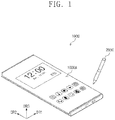
- FIG. 1 illustrates a perspective view showing an electronic device according to some embodiments of the present invention.
- an electronic device 1000 may be an apparatus that is activated with an electronic signal.
- the electronic device 1000 may be a mobile phone, a tablet computer, an automotive navigation system, a game console, or a wearable device, but embodiments according to the present invention are not limited thereto.
- FIG. 1 depicts a mobile phone as an example of the electronic device 1000.
- the electronic device 1000 may display images at an active region 1000A.
- the active region 1000A may include a plane defined by a first direction DR1 and a second direction DR2.
- a thickness direction of the electronic device 1000 may be parallel to a third direction DR3 that intersects the first direction DR1 and the second direction DR2 (e.g., in a direction perpendicular or normal with respect to a plane defined by the first direction DR1 and the second direction DR2).
- the third direction DR3 may be used as a reference to define front and rear surfaces (or top and bottom surfaces) of each of members that constitute the electronic device 1000.
- the electronic device 1000 may detect inputs that are externally applied from outside the electronic device 1000.
- the external inputs may be user's inputs.
- the user's input may include a user's body (e.g., a finger), light, heat, pressure, or various types of external inputs.
- the electronic device 1000 shown in FIG. 1 may detect inputs from a user's touch or an input device 2000.
- the input device 2000 may indicate an apparatus other than a user's body.
- the input device 2000 may be an active pen, a stylus pen, a touch pen, or an electronic pen. The following will describe an example in which an active pen is adopted as the input device 2000.
- the electronic device 1000 and the input device 2000 may each perform two-way communication.
- the electronic device 1000 may provide the input device 2000 with uplink signals.
- the unlink signals may include either synchronization signals or information about the electronic device 1000, but embodiments according to the present invention are not particularly limited thereto.
- the input device 2000 may provide the electronic device 1000 with downlink signals.
- the downlink signals may include either synchronization signals or information about states of the input device 2000.
- the downlink signals may include coordinate information of the input device 2000, battery information of the input device 2000, slope information of the input device 2000, and/or various information stored in the input device 2000, but embodiments according to the present invention are not particularly limited thereto.
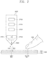
- FIG. 2 illustrates a simplified block diagram showing an input device and an electronic device according to some embodiments of the present invention.
- the electronic device 1000 may include a display layer 100 and a sensor layer 200.
- the display layer 100 may be a component to substantially generate images.
- the display layer 100 may be an emissive display layer, for example, an organic light emitting display layer, a quantum-dot display layer, a micro-led display layer, or a nano-led display layer. Embodiments according to the present disclosure are not limited thereto, however, and the display layer 100 may be any suitable emissive display layer according to the design of the electronic device 1000.
- the sensor layer 200 may be located on the display layer 100.
- the sensor layer 200 may detect external inputs applied from outside.
- the sensor layer 200 may detect not only inputs from a user's body 3000, but also inputs from the input device 2000.
- the user's body 3000 may have an input region of a first width WE1.
- the sensor layer 200 may operate in time-division driving method. For example, the sensor layer 200 may be alternately and repeatedly driven under a first mode and a second mode. An input from the user's body 3000 may be detected in the first mode, and an input from the input device 2000 may be detected in the second mode.
- the sensor layer 200 may provide the input device 2000 with an uplink signal ULS.
- the input device 2000 receives the uplink signal ULS and is synchronized with the electronic device 1000, the input device 2000 may provide the sensor layer 200 with a downlink signal DLS.
- the input device 2000 may include a power source 2100, a memory 2200, a controller 2300, a transmitter 2400, a receiver 2500, and a pen electrode 2600.
- components of the input device 2000 are not limited to those mentioned above.
- the input device 2000 may further include an electrode switch to switch the pen electrode 2600 into a signal transmission mode or a signal reception mode, a pressure sensor to detect pressure, or a rotation sensor to detect rotation.
- the pen electrode 2600 may include a first pen electrode (see, e.g., element 2610 of FIG. 5A ) and a second pen electrode (see, e.g., element 2620 of FIG. 5A ).
- the first pen electrode 2610 may be located at an end of the input device 2000.
- the second pen electrode 2620 may be located at a lateral surface of the input device 2000.
- the sensor layer 200 may obtain a coordinate of the input device 2000 through the first pen electrode 2610, and may also obtain a slope of the input device 2000 through the second pen electrode 2620.
- the pen electrode 2600 may have an input region of a second width WE2.
- the second width WE2 of the input region of the pen electrode 2600 may be less than the first width WE1 of the input region of the user's body 3000.
- the power source 2100 may include one of a battery and a high-capacitance capacitor each of which provides the input device 2000 with power.
- the memory 2200 may store information about functions of the input device 2000.
- the controller 2300 may control an operation of the input device 2000.
- Each of the transmitter 2400 and the receiver 2500 may communicate through the pen electrode 2600 with the electronic device 1000.
- the transmitter 2400 may be called a signal generator or a transmission circuit, and the receiver 2500 may be called a signal receiver or a receiver circuit.
- FIG. 3 illustrates a cross-sectional view showing an electronic device according to some embodiments of the present invention.
- the display layer 100 may include a base layer 110, a circuit layer 120, a light emitting element layer 130, and an encapsulation layer 140.
- the base layer 110 may be a member that provides a base surface on which the circuit layer 120 is located.
- the base layer 110 may be a glass substrate, a metal substrate, or a polymer substrate. However, some embodiments of the present invention are not limited thereto, and the base layer 110 may be an inorganic layer, an organic layer, or a composite material layer.
- the base layer 110 may have a multi-layered structure.
- the base layer 110 may include a first synthetic resin layer, a silicon oxide (SiOx) layer located on the first synthetic resin layer, an amorphous silicon (a-Si) layer located on the silicon oxide layer, and a second synthetic resin layer located on the amorphous silicon layer.
- the silicon oxide layer and the amorphous silicon layer may be called a base barrier layer.
- Each of the first and second synthetic resin layers may include a polyimide-based resin.
- each of the first and second synthetic resin layers may include at least one selected from an acrylate-based resin, a methacrylate-based resin, a polyisoprene-based resin, a vinyl-based resin, an epoxy-based resin, an urethane-based resin, a cellulose-based resin, a siloxane-based resin, a polyamide-based resin, and a perylene-based resin.
- X-based resin may mean a resin including a functional group of X.
- the circuit layer 120 may be located on the base layer 110.
- the circuit layer 120 may include a dielectric layer, a semiconductor pattern, a conductive pattern, a signal line, and the like. Coating and deposition processes may be employed such that a dielectric layer, a semiconductor layer, and a conductive layer are formed on the base layer 110, and then a photolithography process may be performed several times to selectively pattern the dielectric layer, the semiconductor layer, and the conductive layer. Afterwards, there may be formed the semiconductor pattern, the conductive pattern, and the signal line included in the circuit layer 120.
- At least one inorganic layer may be formed on a top surface of the base layer 110.
- the inorganic layer may include at least one selected from aluminum oxide, titanium oxide, silicon oxide, silicon oxynitride, zirconium oxide, and hafnium oxide.
- the inorganic layer may be formed to have a multi-layered structure.
- the multi-layered inorganic layers may constitute a barrier layer and/or a buffer layer.
- the display layer 100 is illustrated to include a buffer layer BFL.
- the buffer layer BFL may increase a bonding force between the base layer 110 and the semiconductor pattern.
- the buffer layer BFL may include a silicon oxide layer and a silicon nitride layer, and the silicon oxide layer and the silicon nitride layer may be alternately stacked.
- the semiconductor pattern may be located on the buffer layer BFL.
- the semiconductor pattern may include polysilicon. Embodiments according to the present invention, however, are not limited thereto, and the semiconductor pattern may include amorphous silicon or metal oxide.
- FIG. 3 merely depicts a portion of the semiconductor pattern, and the semiconductor pattern may further be arranged at other regions.
- the semiconductor pattern may be specifically arranged over pixels.
- the semiconductor pattern may have different electrical characteristics based on whether being doped or not.
- the semiconductor pattern may include a first region whose conductivity is high and a second region whose conductivity is low.
- the first region may be doped with n-type or p-type impurities.
- a p-type transistor may include a doped region implanted with p-type impurities, and an n-type transistor may include a doped region implanted with n-type impurities.
- the second region may be an undoped region or may be implanted with impurities whose concentration is less than that of the impurities implanted into the first region.
- the first region may have conductivity greater than that of the second region, and may substantially serve as an electrode and a signal line.
- the second region may substantially correspond to an active (or channel) of a transistor.
- a portion of the semiconductor pattern may be an active of a transistor, another portion of the semiconductor pattern may be a source or drain of the transistor, and still another portion of the semiconductor pattern may be a connection electrode or a connection signal line.
- Each of the pixels may have an equivalent circuit including seven transistors, one transistor, and a light emitting element, and the equivalent circuit of the pixel may be variously changed.
- FIG. 3 depicts by way of example a pixel including one transistor 100PC and a light emitting element 100PE.
- a source SC1, an active A1, and a drain D1 of the transistor 100PC may be formed of the semiconductor pattern. When viewed in cross-section, the source SC1 and the drain D1 may extend in opposite directions from the active A1.
- FIG. 3 partially shows a connection signal line SCL formed of the semiconductor pattern. According to some embodiments, when viewed in a plan view, the connection signal line SCL may be electrically connected to the drain D1 of the transistor 100PC.
- a first dielectric layer 10 may be located on the buffer layer BFL.
- the first dielectric layer 10 may commonly overlap a plurality of pixels and may cover the semiconductor pattern.
- the first dielectric layer 10 may be one or more of an inorganic layer and an organic layer, and may have a single-layered or multi-layered structure.
- the first dielectric layer 10 may include at least one selected from aluminum oxide, titanium oxide, silicon oxide, silicon oxynitride, zirconium oxide, and hafnium oxide.
- the first dielectric layer 10 may be a single-layered silicon oxide layer.
- the first dielectric layer 10, a dielectric layer of the circuit layer 120 may be one or more of an inorganic layer and an organic layer, and may have a single-layered or multi-layered structure.
- the inorganic layer may include at least one of the materials mentioned above, but embodiments according to the present invention are not limited thereto.
- the transistor 100PC may have a gate G1 located on the first dielectric layer 10.
- the gate G1 may be a portion of a metal pattern.
- the gate G1 may overlap the active A1.
- the gate G1 may serve as a mask when the semiconductor pattern is doped.
- a second dielectric layer 20 may be located on the first dielectric layer 10 and may cover the gate G1.
- the second dielectric layer 20 may commonly overlap the pixels.
- the second dielectric layer 20 may be one or more of an inorganic layer and an organic layer, and may have a single-layered or multi-layered structure. In some embodiments, the second dielectric layer 20 may be a single-layered silicon oxide layer.
- a third dielectric layer 30 may be located on the second dielectric layer 20, and in some embodiments, the third dielectric layer 30 may be a single-layered silicon oxide layer
- a first connection electrode CNE1 may be located on the third dielectric layer 30.
- the first connection electrode CNE1 may be coupled to a connection signal line SCL through a contact hole CNT-1 that penetrates the first, second, and third dielectric layers 10, 20, and 30.
- a fourth dielectric layer 40 may be located on the third dielectric layer 30.
- the fourth dielectric layer 40 may be a single-layered silicon oxide layer.
- a fifth dielectric layer 50 may be located on the fourth dielectric layer 40.
- the fifth dielectric layer 50 may be an organic layer.
- a second connection electrode CNE2 may be located on the fifth dielectric layer 50.
- the second connection electrode CNE2 may be coupled to the first connection electrode CNE1 through a contact hole CNT-2 that penetrates the fourth and fifth dielectric layers 40 and 50.
- a sixth dielectric layer 60 may be located on the fifth dielectric layer 50 and may cover the second connection electrode CNE2.
- the sixth dielectric layer 60 may be an organic layer.
- the light emitting element layer 130 may be located on the circuit layer 120.
- the light emitting element layer 130 may include a light emitting element 100PE.
- the light emitting element layer 130 may include an organic light emitting material, a quantum dot, a quantum rod, a micro-led, or a nano-led.
- the light emitting element 100PE may include a first electrode AE, an emission layer EL, and a second electrode CE.
- the first electrode AE may be located on the sixth dielectric layer 60.
- the first electrode AE may be connected to the second connection electrode CNE2 through a contact hole CNT-3 that penetrates the sixth dielectric layer 60.
- a pixel definition layer 70 may be located on the sixth dielectric layer 60 and may cover a portion of the first electrode AE.
- An opening 70-OP may be defined in the pixel definition layer 70.
- the opening 70-OP of the pixel definition layer 70 may expose at least a portion of the first electrode AE.
- a light emitting region PXA may be defined to correspond to the portion of the first electrode AE, which portion is exposed to the opening 70-OP.
- a non-light emitting region NPXA may surround the light emitting region PXA.
- the emission layer EL may be located on the first electrode AE.
- the emission layer EL may be located in the opening 70-OP.
- a plurality of emission layers EL may be formed on corresponding pixels.
- the emission layers EL may each emit light having at least one of blue, red, or green colors.
- the emission layer EL may be provided which is commonly connected to the pixels. In this case, the emission layer EL may provide a blue light or a white light.
- the second electrode CE may be located on the emission layer EL.
- the second electrode CE may be commonly located on a plurality of pixels, while having a single unitary shape.
- the second electrode CE may be supplied with a common voltage and may be called a common electrode.
- a hole control layer may be located between the first electrode AE and the emission layer EL.
- the hole control layer may be commonly located on the light emitting region PXA and the non-light emitting region NPXA.
- the hole control layer may include a hole transport layer and may further include a hole injection layer.
- An electrode control layer may be located between the emission layer EL and the second electrode CE.
- the electrode control layer may include an electrode transport layer and may further include an electrode injection layer.
- An open mask may be used to form the hole control layer and the electrode control layer that are commonly arranged on a plurality of pixels.
- the encapsulation layer 140 may be located on the light emitting element layer 130.
- the encapsulation layer 140 may include an inorganic layer, an organic layer, and an inorganic layer that are sequentially stacked, but no limitation is imposed on the constituent layers of the encapsulation layer 140.
- the inorganic layers may protect the light emitting element layer 130 against moisture and oxygen, and the organic layer may protect the light emitting element layer 130 against foreign substances such as dust particles.
- the inorganic layers may include a silicon nitride layer, a silicon oxynitride layer, a silicon oxide layer, a titanium oxide layer, or an aluminum oxide layer.
- the organic layer may include an acryl-based organic layer, but embodiments according to the present invention are not limited thereto.
- a successive process may be employed to form the sensor layer 200 on the display layer 100.
- the sensor layer 200 is directly arranged on the display layer 100.
- the phrase "directly arranged on” or “directly located on” may mean that no third component is located between the sensor layer 200 and the display layer 100.
- no adhesive member may be separately located between the sensor layer 200 and the display layer 100.
- the electronic device 1000 may decrease in thickness.
- the sensor layer 200 may include a base dielectric layer 201, a first conductive layer 202, a sensing dielectric layer 203, a second conductive layer 204, and a cover dielectric layer 205.
- the base dielectric layer 201 may be an inorganic layer that includes one of silicon nitride, silicon oxynitride, and silicon oxide. Alternatively, the base dielectric layer 201 may be an organic layer that includes an epoxy-based resin, an acryl-based resin, or an imide-based resin. The base dielectric layer 201 may have either a single-layered structure or a multi-layered structure stacked along the third direction DR3.
- Each of the first and second conductive layers 202 and 204 may have either a single-layered structure or a multi-layered structure stacked along the third direction DR3.
- the single-layered conductive layer may include a metal layer or a transparent conductive layer.
- the metal layer may include molybdenum, silver, titanium, copper, aluminum, or an alloy thereof.
- the transparent conductive layer may include transparent conductive oxide, such as indium tin oxide (ITO), indium zinc oxide (IZO), zinc oxide (ZnO), indium zinc tin oxide (IZTO). Additionally or alternatively, the transparent conductive layer may include a metal nano-wire, a graphene, or a conductive polymer such as PEDOT.
- the multi-layered conductive layer may include metal layers.
- the metal layers may include, for example, tri-layered structure of titanium/aluminum/titanium.
- the multi-layered conductive layer may include at least one metal layer and at least one transparent conductive layer.
- the sensing dielectric layer 203 and the cover dielectric layer 205 may include an inorganic layer.
- the inorganic layer may include at least one selected from aluminum oxide, titanium oxide, silicon oxide, silicon oxynitride, zirconium oxide, and hafnium oxide.
- a parasitic capacitance Cb may occur between the sensor layer 200 and the second electrode CE.
- a reduction in distance between the sensor layer 200 and the second electrode CE may induce an increase in the parasitic capacitance Cb.
- the greater the parasitic capacitance Cb the smaller ratio of variation in capacitance with respect to the reference value.
- the variation in capacitance may indicate a capacitance change that occurs between before and after an input from an input means, for example, the input device (see, e.g., element 2000 of FIG. 2 ) or the user's body (see, e.g., element 3000 of FIG. 2 ).
- a driver chip that processes signals detected from the sensor layer 200 may perform a leveling operation in which a value corresponding to the parasitic capacitance Cb is removed from the detected signal.
- the leveling operation may increase the ratio of variation in capacitance with respect to a reference value, and therefore detection sensitivity may be improved.
- the capability of removing the value corresponding to the parasitic capacitance Cb may depend on a specification of the driver chip. For example, when about 500 pF is assigned to a maximum value of the parasitic capacitance Cb, and when about 200 pF is given to a value of the parasitic capacitance Cb that the driver chip can remove from a signal detected from the sensor layer 200, the reference value may not be sufficiently reduced by the driver chip. In this case, the ratio of variation in capacitance may be insignificant compared to the reference value, and thus the driver chip may not detect the variation in capacitance or may consider the variation in capacitance as noise, which may result in malfunction that fails to detect a touch coordinate.
- an electrode structure of the sensor layer 200 may be changed such that the maximum value of the parasitic capacitance Cb may be reduced below a certain value.
- the certain value may be about 200 pF, but embodiments according to the present invention are not particularly limited thereto.
- FIG. 4 illustrates a plan view showing a sensor layer according to some embodiments of the present invention.
- the sensor layer 200 may include an active region 200A and a peripheral region 200N.
- the active region 200A may be an area that is activated with an electric signal.
- the active region 200A may be an input detection section.
- the active region 200A may be called a sensing region.
- the peripheral region 200N may surround the active region 200A.
- the sensor layer 200 may include a base dielectric layer 201, a plurality of sensing units 210, and a plurality of wiring lines 220.
- the plurality of sensing units 210 may be located on the active region 200A.
- the plurality of wiring lines 220 may be located on the peripheral region 200N.
- the plurality of sensing units 210 may have a first pitch PC1.
- the first pitch PC1 of the plurality of sensing units 210 may be less than the first width WE1 of the input region of the user's body 3000 (see FIG. 2 ).
- the first pitch PC1 may range from about 3.5 mm to about 4.5 mm.
- the first pitch PC1 may be about 4 mm.
- each of the plurality of sensing units 210 may have an area less than that of the input region of the user's body 3000. Therefore, the sensor layer 200 may exactly detect coordinates that are input by the user's body 3000.
- Each of the plurality of sensing units 210 may include a plurality of sub-sensing units SU. As discussed below in FIG. 5A , an electrode 211 and a cross electrode 212 may intersect each other at each of the plurality of sub-sensing units SU.
- the plurality of sub-sensing units SU may have a second pitch PC2.
- the second pitch PC2 of the plurality of sub-sensing units SU may be less than the second width WE2 of the pen electrode 2600 included in the input device 2000 (see FIG. 2 ).
- the second pitch PC2 may range from about 1.0 mm to about 2.0 mm.
- the second pitch PC2 may be about 1.5 mm.
- each of the plurality of sub-sensing units SU may have an area less than that of the input region of the pen electrode 2600 included in the input device 2000. Therefore, the sensor layer 200 may exactly detect coordinates that are input by the input device 2000.
- the sensor layer 200 may operate under the first mode in which information about external inputs are obtained based on a variation in mutual capacitance between electrodes included in the plurality of sensing units 210, or under the second mode in which inputs from the input device 2000 are detected based on a variation in capacitance of each of electrodes included in the plurality of sub-sensing units SU.
- the first and second modes will be further discussed in detail below.
- the plurality of sensing units 210 may be arranged along the first direction DR1 and the second direction DR2.
- the plurality of wiring lines 220 may be electrically connected to the plurality of sub-sensing units SU.
- FIG. 5A illustrates a plan view showing one of a plurality of sensing units according to some embodiments of the present invention.
- FIG. 5B illustrates a plan view showing one of a plurality of sub-sensing units according to some embodiments of the present invention.
- a single sensing unit 210 may include a plurality of sub-sensing units SU.
- the plurality of sub-sensing units SU may be arranged in the first direction DR1 and the second direction DR2. For example, nine sub-sensing units SU may be provided.
- the sensing unit 210 may include a plurality of electrodes 211, a plurality of cross electrodes 212, and a dummy electrode 213.
- the plurality of electrodes 211, the plurality of cross electrodes 212, and the dummy electrode 213 may have their mesh structures.
- the sensor layer may obtain information about external inputs.
- Each of the plurality of electrodes 211 may extend in the first direction DR1.
- the plurality of electrodes 211 may be arranged spaced apart from each other in the second direction DR2.
- Each of the plurality of cross electrodes 212 may extend in the second direction DR2.
- the plurality of cross electrodes 212 may be arranged spaced apart from each other in the first direction DR1.
- the plurality of electrodes 211 may intersect the plurality of cross electrodes 212.
- a plurality of dummy electrodes 213 may surround the plurality of electrodes 211 and the plurality of cross electrodes 212.
- the presence of the dummy electrodes 213 may reduce a difference in transmittance or reflectance between portions having the plurality of electrodes 211 or cross electrodes 212 and portions not having the plurality of electrodes 211 or cross electrodes 212.
- Each of the plurality of electrodes 211 may include a first portion 211P1 and a plurality of second portions 211P2.
- the first portion 211P1 may extend in the first direction DR1.
- the plurality of second portions 211P2 may protrude from the first portion 211P1.
- the first portion 211P1 and the plurality of second portions 211P2 may be provided unitarily with each other.
- the plurality of second portions 211P2 may include a plurality of first pattern portions 211PP1, a plurality of second pattern portions 211PP2, and a plurality of third pattern portions 211PP3.
- Each of the plurality of first pattern portions 211PP1 may protrude from the first portion 211P1.
- each of the plurality of first pattern portions 211PP1 may protrude in the second direction DR2 from the first portion 211P1.
- a single sub-sensing unit SU may include four first pattern portions 211PP1.
- the plurality of second pattern portions 211PP2 may each protrude from the plurality of first pattern portions 211PP1 in a direction adjacent to a first cross portion 212P1 which will be discussed below.
- the plurality of second pattern portions 211PP2 may each protrude in the first direction DR1 from the plurality of first pattern portions 211PP1.
- a single sub-sensing unit SU may include four second pattern portions 211PP2.
- Each of the plurality of first pattern portions 211PP1 may have an end adjacent to the first portion 211P1 and other end adjacent to one of the plurality of second pattern portions 211PP2.
- the first pattern portion 211PP1 and the second pattern portion 211PP2 may be provided unitarily with each other.
- Each of the plurality of third pattern portions 211PP3 may protrude from the first portion 211P1 in a first cross direction DRa or a second cross direction DRb.
- the first cross direction DRa may intersect the first direction DR1 and the second direction DR2.
- the second cross direction DRb may intersect the first cross direction DRa.
- the first cross direction DRa and the second cross direction DRb may be orthogonal to each other.
- a single sub-sensing unit SU may include four third pattern portions 211PP3.
- the plurality of cross electrodes 212 may include a plurality of cross patterns 212PT and a plurality of bridge patterns 212B.
- Each of the plurality of cross patterns 212PT may include a first cross pattern 212PT1 and a second cross pattern 212PT2 that are spaced apart from each other across the first portion 211P1.
- the first cross pattern 212PT1 and the second cross pattern 212PT2 may have their shapes that are symmetrical with each other about a first axis AX1 that extends along the first direction DR1.
- Each of the first and second cross patterns 212PT1 and 212PT2 may include a first cross portion 212P1 and a plurality of second cross portions 212P2.
- the first cross portion 212P1 may extend in the second direction DR2.
- the plurality of second cross portions 212P2 may protrude from the first cross portion 212P1.
- the first cross portion 212P1 and the plurality of second cross portions 212P2 may be provided unitarily with each other.
- the plurality of second cross portions 212P2 may include a plurality of first cross pattern portions 212PP1 and a plurality of second cross pattern portions 212PP2.
- the plurality of first cross pattern portions 212PP1 may surround the plurality of first pattern portions 211PP1 and the plurality of second pattern portions 211PP2.
- Each of the plurality of first cross pattern portions 212PP1 may include a first section and a second section.
- the second section may extend in the second direction DR2 and may be spaced apart in the first direction DR1 from the first cross portion 212P1.
- the second section may be adjacent to one of the plurality of second pattern portions 211PP2.
- the first section may be located between the first cross portion 212P1 and the second section.
- the first section may be adjacent to one of the plurality of first pattern portions 211PP1.
- the first section and the second section may be provided unitarily with each other.
- a single sub-sensing unit SU may include four first cross pattern portions 212PP1.
- the plurality of second cross pattern portions 212PP2 may protrude in a direction that faces the plurality of third pattern portions 211PP3. Each of the plurality of second cross pattern portions 212PP2 may protrude from the first cross portion 212P1 in the first cross direction DRa or the second cross direction DRb. The plurality of second cross pattern portions 212PP2 may be located adjacent to the plurality of third pattern portions 211PP3. For example, a single sub-sensing unit SU may include four second cross pattern portions 212PP2.
- the plurality of bridge patterns 212B may be electrically connected to the plurality of cross patterns 212PT.
- the plurality of bridge patterns 212B may be insulated from and intersect the first portion 211P1.
- the plurality of bridge patterns 212B may extend in the first cross direction DRa and the second cross direction DRb.
- the plurality of bridge patterns 212B may have their mesh structures.
- Each of the plurality of bridge patterns 212B may electrically connect the first cross pattern 212PT1 to the second cross pattern 212PT2.
- the plurality of bridge patterns 212B may be located at a level from that of the plurality of electrodes 211 and that of the plurality of cross patterns 212PT.
- the dummy electrode 213 may include a plurality of first dummy portions 213P1 and a plurality of second dummy portions 213P2.
- the plurality of first dummy portions 213P1 may be located between the plurality of first pattern portions 211PP1, the plurality of second pattern portions 211PP2, the plurality of third pattern portions 211PP3, and the plurality of first cross pattern portions 212PP1.
- the plurality of second dummy portions 213P2 may be located adjacent to the first portion 211P1, the first cross portion 212P1, and the plurality of first cross pattern portions 212PP1.
- the first cross pattern 212PT1 of one sub-sensing unit SU may be provided unitarily with the second cross pattern 212PT2 of another sub-sensing unit SU adjacent in the second direction DR2 to the one sub-sensing unit SU.
- the electrodes 211 of two sub-sensing units SU adjacent to each other in the second direction DR2 may be called a first electrode and a second electrode
- the first cross pattern 212PT1 of one of the two sub-sensing units SU and the second cross pattern 212PT2 of the other of the two subs-sensing units SU may be called a third electrode.
- the sensor layer 200 may include the plurality of sensing units 210 that are repeatedly arranged at the first pitch PC1 less than the first width WE1 of the input region of the user's body 3000 (see FIG. 2 ). Each of the plurality of sensing units 210 may have an area less than that of the input region of the user's body 3000.
- the sensing unit 210 when the user's body 3000 is detected, the sensing unit 210 may be located within the coverage of the input region of the user's body 3000 that overlaps the sensor layer 200. It may be possible to normally detect a variation in mutual capacitance between the plurality of cross electrodes 212 and the plurality of electrodes 211 when the user's body 3000 is detected. Therefore, the sensor layer 200 may increase in detection reliability and coordinate accuracy for the user's body 3000.
- the sensor layer 200 may include the plurality of sub-sensing units SU that are repeatedly arranged at the second pitch PC2 less than the second width WE2 of the input region of the pen electrode 2600 included in the input device 2000 (see FIG. 2 ).
- An input region of the input device 2000 may have an area less than that of each of the plurality of sub-sensing units SU.
- the electrode 211 and the cross electrode 212 may intersect each other at each of the plurality of sub-sensing units SU.
- a pitch of the sensing unit 210 may be greater than the second width WE2 of the input region of the pen electrode 2600 included in the input device 2000.
- the sub-sensing unit SU when the input device 2000 is detected, the sub-sensing unit SU may be located within the coverage of the input region of the input device 2000 that overlaps the sensor layer 200.
- a reduced difference may be provided between the first capacitance CAP1a detected by the first pen electrode 2610 when the input device 2000 is placed at the first position and the second capacitance CAP1b detected by the first pen electrode 2610 when the input device 2000 is placed at the second position.
- a reduced difference may be provided between a first capacitance CAP2a detected by the second pen electrode 2620 when the input device 2000 is placed at the first position and a second capacitance CAP2b detected by the second pen electrode 2620 when the input device 2000 is placed at the second position.
- a reduced deviation in capacitance between the sensor layer 200 and the input device 2000 which deviation depends on the position of the input device 2000. Therefore, the sensor layer 200 may increase in slope accuracy and detection reliability for the input device 2000.
- FIG. 6A illustrates a cross-sectional view taken along line I-I' of FIG. 5A .
- the same reference symbols are allocated to the components discussed in FIGS. 5A and 5B , and some repetitive description thereof may be omitted.
- the bridge pattern 212B may be located on the base dielectric layer 201.
- the sensing dielectric layer 203 may be located on the bridge pattern 212B.
- the sensing dielectric layer 203 may cover the bridge pattern 212B.
- the sensing dielectric layer 203 may include an inorganic material, an organic material, or a composite material.
- the first cross pattern 212PT1, the second cross pattern 212PT2, and the electrode 211 may be located on the sensing dielectric layer 203.
- a plurality of first contact holes CNT1 may be formed to penetrate the sensing dielectric layer 203 in the third direction DR3.
- the first cross pattern 212PT1 and the second cross pattern 212PT2 may be electrically connected to the bridge pattern 212B through the plurality of first contact holes CNT1.
- the cover dielectric layer 205 may be located on the first cross pattern 212PT1, the second cross pattern 212PT2, and the electrode 211.
- the cover dielectric layer 205 may cover the first cross pattern 212PT1, the second cross pattern 212PT2, and the electrode 211.
- the cover dielectric layer 205 may include an inorganic material, an organic material, or a composite material.
- FIG. 6A depicts by way of example a bottom bridge structure in which the bridge pattern 212B is located below the first cross pattern 212PT1, the second cross pattern 212PT2, and the electrode 211, but according to some embodiments of the present invention, the structure of the sensor layer (see, e.g., element 200 of FIG. 4 ) is not limited to that mentioned above.
- the sensor layer 200 according to some embodiments of the present invention may have a top bridge structure in which the bridge pattern 212B is located above the first cross pattern 212PT1, the second cross pattern 212PT2, and the electrode 211.
- FIG. 6B illustrates a cross-sectional view taken along line II-II' of FIG. 4
- the same reference symbols are allocated to the components discussed in FIG. 6A , and some repetitive description thereof may be omitted.
- each of the plurality of wiring lines 220 may include a first line part 220P1 and a second line part 220P2.
- the first line part 220P1 may be located on the base dielectric layer 201.
- the sensing dielectric layer 203 may be located on the first line part 220P1.
- the sensing dielectric layer 203 may cover the first line part 220P1.
- the second line part 220P2 may be located on the first line part 220P1.
- a plurality of second contact holes CNT2 may be formed to penetrate the sensing dielectric layer 203 in the third direction DR3.
- the first line part 220P1 and the second line part 220P2 may be connected to each other through the plurality of second contact holes CNT2.
- the cover dielectric layer 205 may be located on the second line part 220P2.
- the cover dielectric layer 205 may cover the second line part 220P2.
- FIG. 6B depicts by way of example a structure in which the first line part 220P1 and the second line part 220P2 are connected to each other, but according to some embodiments of the present invention, the structure of the sensor layer (see, e.g., element 200 of FIG. 4 ) is not limited to that mentioned above.
- the sensing dielectric layer 203 may not include a plurality of second contact holes CNT2.
- the first line part 220P1 and the second line part 220P2 may be arranged to be spaced apart from each other in the third direction DR3.
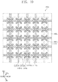
- FIG. 7 illustrates a plan view showing one of a plurality of sensing units according to some embodiments of the present invention.
- the same reference symbols are allocated to the components discussed in FIGS. 5A and 5B , and some repetitive description thereof may be omitted.
- one sensing unit 210a may include a plurality of sub-sensing units SUa.
- the plurality of sub-sensing units SUa may be arranged in the first direction DR1 and the second direction DR2.
- twenty-five sub-sensing units SUa may be provided.
- Embodiments according to the present invention are not limited thereto, and no limitation is imposed on the number of the plurality of sub-sensing units SUa according to some embodiments of the present invention.
- sixteen sub-sensing units SUa may be provided.
- the plurality of sub-sensing units SUa may have a second pitch PC2a.
- the second pitch PC2a of the plurality of sub-sensing units SUa may be less than the second width WE2 of the input region of the pen electrode 2600 included in the input device 2000 (see FIG. 2 ).
- the second pitch PC2a may be less than the second pitch (see, e.g., element PC2 of FIG. 4 ) of the plurality of sub-sensing units (see, e.g., element SU of FIG. 5A ).
- An input region of the input device 2000 may have an area less than that of each of the plurality of sub-sensing units SUa.
- the sub-sensing unit SUa when the input device 2000 is detected, the sub-sensing unit SUa may be located within the coverage of the input region of the input device 2000 that overlaps the sensor layer (see, e.g., element 200 of FIG. 4 ). Despite movement of the input device 2000, it may be possible for the sensor layer 200 to normally detect capacitance of each of the first portion 211P1, the second portion 211P2, the first cross portion 212P1, and the second cross portion 212P2. Therefore, the sensor layer 200 may increase in detection reliability for the input device 2000.
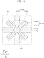
- FIG. 8 illustrates a plan view showing one of a plurality of sub-sensing units according to some embodiments of the present invention.
- the same reference symbols are allocated to the components discussed with reference to FIG. 5B , and some repetitive description thereof may be omitted.
- a first portion 211P1b may extend in the first direction DR1.
- a plurality of second portions 211P2b may protrude from the first portion 211P1b.
- the first portion 211P1b and the plurality of second portions 211P2b may be provided unitarily with each other.
- the first portion 211P1b and the plurality of second portions 211P2b may have their mesh structures.
- the plurality of second portions 211P2b may include a plurality of first pattern portions 211PP1b and a plurality of second pattern portions 211PP2b.
- Each of the plurality of first pattern portions 211PP1b may protrude from the first portion 211P1b.
- each of the plurality of first pattern portions 211PP1b may protrude in the first cross direction DRa.
- the first cross direction DRa may intersect the first direction DR1 and the second direction DR2.
- Each of the plurality of second pattern portions 211PP2b may protrude from the first portion 211P1b.
- each of the plurality of second pattern portions 211PP2b may protrude in the second cross direction DRb.
- the second cross direction DRb may intersect the first direction DR1 and the second direction DR2.
- the second cross direction DRb may intersect the first cross direction DRa.
- the first cross direction DRa and the second cross direction DRb may be orthogonal to each other.
- a plurality of cross patterns 212PTb may be spaced apart from each other across the first portion 211P1b.
- the plurality of cross patterns 212PTb may be symmetrical with each other about the first axis AX1.
- the plurality of cross patterns 212PTb may include a first cross portion 212P1b and a plurality of second cross portions 212P2b.
- the first cross portion 212P1b may extend in the second direction DR2.
- the plurality of second cross portions 212P2b may protrude from the first cross portion 212P1b.
- the first cross portion 212P1b and the plurality of second cross portions 212P2b may be provided unitarily with each other.
- the first cross portion 212P1b and the plurality of second cross portions 212P2b may have their mesh structures.
- the plurality of second cross portions 212P2b may correspondingly surround the plurality of second portions 211P2b.
- One of the plurality of second cross portions 212P2b may protrude in the first cross direction DRa and may be located adjacent to the plurality of first pattern portions 211PP1b.
- Another of the plurality of second cross portions 212P2b may protrude in the second cross direction DRb and may be located adjacent to the plurality of second pattern portions 211PP2b.
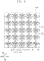
- FIG. 9 illustrates a plan view showing one of a plurality of sensing units according to some embodiments of the present invention.
- the same reference symbols are allocated to the components discussed with reference to FIG. 8 , and some repetitive description thereof may be omitted.
- each of a plurality of sensing units 210b may include a first region AR1, a plurality of second regions AR2 that are adjacent in the first direction DR1 to the first region AR1, a plurality of third regions AR3 that are adjacent in the second direction DR2 to the first region AR1, and a plurality of fourth regions AR4 that are spaced apart from the first region AR1 in the first cross direction DRa and the second cross direction DRb.
- the first region AR1 may be provided thereon with a plurality of first portions 211P1b, a plurality of second portions 211P2b, a plurality of cross patterns 212PTb, a plurality of bridge patterns 212B, and a dummy electrode 213.
- the plurality of second regions AR2 may be provided thereon with a plurality of first portions 211P1b, a plurality of second portions 211P2b, and a dummy electrode 213.
- neither the plurality of cross patterns 212PTb nor the plurality of bridge patterns 212B may overlap the plurality of second regions AR2.
- the plurality of third regions AR3 may be provided thereon with a plurality of cross patterns 212PTb, a plurality of bridge patterns 212B, and a dummy electrode 213.
- a plurality of cross patterns 212PTb may overlap the plurality of third regions AR3.
- the plurality of fourth regions AR4 may be provided thereon with a dummy electrode 213.
- FIG. 10 illustrates a plan view showing one of a plurality of sensing units according to some embodiments of the present invention.
- the same reference symbols are allocated to the components discussed in FIG. 8 , and some repetitive description thereof may be omitted.
- each of a plurality of sensing units 210c may include a first region AR1a and a second region AR2a that surrounds the first region AR1a.
- the first region AR1a may be provided thereon with a plurality of first portions 211P1b, a plurality of second portions 211P2b, a plurality of cross patterns 212PTb, a plurality of bridge patterns 212B, and a dummy electrode 213.
- the second region AR2a may be provided thereon with a plurality of first portions 211P1 b, a plurality of first cross portions 212P1b, and a dummy electrode 213.
- FIG. 11 illustrates a plan view showing one of a plurality of sub-sensing units according to some embodiments of the present invention.
- the same reference symbols are allocated to the components discussed with reference to FIG. 5B , and some repetitive description thereof may be omitted.
- a first portion 211P1c may extend in the first direction DR1.
- a plurality of second portions 211P2c may protrude from the first portion 211P1c.
- the first portion 211P1c and the plurality of second portions 211P2c may be provided unitarily with each other.
- the first portion 211P1c and the plurality of second portions 211P2c may have their mesh structures.
- the plurality of second portions 211P2c may include a plurality of first pattern portions 211PP1c and a plurality of second pattern portions 211PP2c.
- Each of the plurality of first pattern portions 211PP1c may protrude from the first portion 211P1c.
- Each of the plurality of first pattern portions 211PP1c may include a first section and a second section.
- the first section may protrude in the second direction DR2 from the first portion 211P1c.
- An end of the first section may be adjacent to the first portion 211P1c.
- the second section may protrude in the first direction DR1 from other end of the first section.
- the first section and the second section may be provided unitarily with each other.
- the plurality of first pattern portions 211PP1c may correspondingly surround a plurality of first cross pattern portions 212PP1c and a plurality of second cross pattern portions 212PP2c.
- Each of the plurality of second pattern portions 211PP2c may protrude from the first portion 211P1c.
- Each of the plurality of second pattern portions 211PP2c may include a third section and a fourth section.
- the third section may protrude in the second direction DR2 from the first portion 211P1c.
- An end of the third section may be adjacent to the first portion 211P1c.
- the fourth section may protrude in the first direction DR1 from other end of the third section.
- the third section and the fourth section may be provided unitarily with each other.
- the plurality of second pattern portions 211PP2c may be correspondingly spaced apart from the plurality of first pattern portions 211PP1c across the plurality of first cross pattern portions 212PP1c and the plurality of second cross pattern portions 212PP2c.
- a plurality of cross patterns 212PTc may be spaced apart from each other across the first portion 211P1c.
- the plurality of cross patterns 212PTc may be symmetrical with each other about the first axis AX1.
- the plurality of cross patterns 212PTc may include a first cross portion 212P1c and a plurality of second cross portions 212P2c.
- the first cross portion 212P1c may extend in the second direction DR2.
- the plurality of second cross portions 212P2c may protrude from the first cross portion 212P1c.
- the first cross portion 212P1c and the plurality of second cross portions 212P2c may be provided unitarily with each other.
- the first cross portion 212P1c and the plurality of second cross portions 212P2c may have their mesh structures.
- the plurality of second cross portions 212P2c may be located between the plurality of first pattern portions 211PP1c and the plurality of second pattern portions 211PP2c.
- the plurality of second cross portions 212P2c may include the plurality of first cross pattern portions 212PP1c and the plurality of second cross pattern portions 212PP2c.
- Each of the plurality of first cross pattern portions 212PP1c may protrude from the first cross portion 212P1c.
- each of the plurality of first cross pattern portions 212PP1c may protrude in the first direction DR1 from the first cross portion 212P1c.
- the plurality of second cross pattern portions 212PP2c may protrude from the plurality of first cross pattern portions 212PP1c in a direction adjacent to the first portion 211P1c.
- the plurality of second cross pattern portions 212PP2c may protrude in the second direction DR2 from the plurality of first cross pattern portions 212PP1c.
- Each of the plurality of first cross pattern portions 212PP1c may have one end adjacent to the first cross portion 212P1c and other end adjacent to one of the plurality of second cross pattern portions 212PP2c.
- the plurality of second cross portions 212P2b may surround the plurality of second portions 211P2b.
- One of the plurality of second cross portions 212P2b may protrude in the first cross direction DRa and may be located adjacent to the plurality of first pattern portions 211PP1b.
- Another of the plurality of second cross portions 212P2b may protrude in the second cross direction DRb and may be located adjacent to the plurality of second pattern portions 211PP2b.
- FIG. 12 illustrates a plan view showing one of a plurality of sub-sensing units according to some embodiments of the present invention.
- the same reference symbols are allocated to the components discussed with reference to FIG. 5B , and some repetitive description thereof may be omitted.
- a first portion 211P1d may extend in the first direction DR1.
- a plurality of second portions 211P2d may protrude from the first portion 211P1d.
- the first portion 211P1d and the plurality of second portions 211P2d may be provided unitarily with each other.
- the first portion 211P1d and the plurality of second portions 211P2d may have their mesh structures.
- the plurality of second portions 211P2d may include a plurality of first pattern portions 211PP1d and a plurality of second pattern portions 211PP2d.
- Each of the plurality of first pattern portions 211PP1d may protrude from the first portion 211P1d.
- each of the plurality of first pattern portions 211PP1d may protrude in the first cross direction DRa.
- Each of the plurality of second pattern portions 211PP2d may protrude from the first portion 211P1d.
- each of the plurality of second pattern portions 211PP2d may protrude in the second cross direction DRb.
- Each of a plurality of cross patterns 212PTd may be spaced apart from each other across the first portion 211P1d.
- the plurality of cross patterns 212PTd may be symmetrical with each other about the first axis AX1.
- the plurality of cross patterns 212PTd may include a first cross portion 212P1d and a plurality of second cross portions 212P2d.
- the first cross portion 212P1d may extend in the second direction DR2.
- the plurality of second cross portions 212P2d may protrude from the first cross portion 212P1d.
- the first cross portion 212P1d and the plurality of second cross portions 212P2d may be provided unitarily with each other.
- the first cross portion 212P1d and the plurality of second cross portions 212P2d may have their mesh structures.
- the plurality of second cross portions 212P2d may include a plurality of first cross pattern portions 212PP1d and a plurality of second cross pattern portions 212PP2d.
- Each of the plurality of first cross pattern portions 212PP1d may protrude from the first cross portion 212P1d.
- the plurality of first cross pattern portions 212PP1d may protrude in the first cross direction DRa.
- the plurality of first cross pattern portions 212PP1d may be correspondingly located adjacent to the plurality of first pattern portions 211PP1d.
- the plurality of second cross pattern portions 212PP2d may protrude from the plurality of first cross portions 212P1d.
- the plurality of second cross pattern portions 212PP2d may protrude in the second cross direction DRb.
- the plurality of second cross pattern portions 212PP2d may be correspondingly located adjacent to the plurality of second pattern parts 211PP2d.
- FIG. 13 illustrates a plan view showing one of a plurality of sub-sensing units according to some embodiments of the present invention.
- the same reference symbols are allocated to the components discussed with reference to FIG. 8 , and some repetitive description thereof may be omitted.
- a dummy electrode 213e may include a plurality of first dummy portions 213P1e and a plurality of second dummy portions 213P2e.
- the plurality of first dummy portions 213P1e may correspondingly surround a plurality of first pattern portions 211PP1b and a plurality of second pattern portions 211PP2b.
- the plurality of first dummy portions 213P1e may be correspondingly located between a plurality of second cross portions 212P2e and a plurality of second portions 211P2b.
- the plurality of second dummy portions 213P2e may be located adjacent to a first portion 211P1b, a first cross portion 212P1e, and the plurality of second cross portions 212P2e.
- a plurality of cross patterns 212PTe may include the first cross portion 212P1e and the plurality of second cross portions 212P2e.
- the first cross portion 212P1e may extend in the second direction DR2.
- the plurality of second cross portions 212P2e may protrude from the first cross portion 212P1e.
- the first cross portion 212P1e and the plurality of second cross portions 212P2e may be provided unitarily with each other.
- the first cross portion 212P1e and the plurality of second cross portions 212P2e may have their mesh structures.
- the plurality of second cross portions 212P2e may correspondingly surround the plurality of first dummy portions 213P1e.
- FIG. 14 illustrates a plan view showing one of a plurality of sub-sensing units according to some embodiments of the present invention.
- the same reference symbols are allocated to the components discussed in FIG. 12 , and some repetitive description thereof may be omitted.
- a dummy electrode 213f may include a plurality of first dummy portions 213P1f, a plurality of second dummy portions 213P2f, and a plurality of third dummy parts 213P3f.
- the plurality of first dummy portions 213P1f may be correspondingly located between a plurality of first pattern portions 211PP1d and a plurality of first cross pattern portions 212PP1f.
- the plurality of second dummy portions 213P2f may be correspondingly located between a plurality of second pattern portions 211PP2d and a plurality of second cross pattern portions 212PP2f.
- the plurality of third dummy parts 213P3f may be located adjacent to a first portion 211P1d, a plurality of second portions 211P2d, and a plurality of cross patterns 212PTf.
- the plurality of cross patterns 212PTf may include a first cross portion 212P1f and a plurality of second cross portions 212P2f.
- the first cross portion 212P1f may extend in the second direction DR2.
- the plurality of second cross portions 212P2f may protrude from the first cross portion 212P1f.
- the first cross portion 212P1f and the plurality of second cross portions 212P2f may be provided unitarily with each other.
- the first cross portion 212P1f and the plurality of second cross portions 212P2f may have their mesh structures.
- the plurality of second cross portions 212P2f may include a plurality of first cross pattern portions 212PP1f and a plurality of second cross pattern portions 212PP2f.
- the plurality of first cross pattern portions 212PP1f may be correspondingly spaced apart from the plurality of first pattern portions 211PP1d across the plurality of first dummy portions 213P1f.
- the plurality of second cross pattern portions 212PP2f may be correspondingly spaced apart from the plurality of second pattern portions 211PP2d across the plurality of second dummy portions 213P2f.
- FIG. 15 illustrates a plan view showing one of a plurality of sub-sensing units according to some embodiments of the present invention.
- the same reference symbols are allocated to the components discussed with reference to FIG. 5B , and some repetitive description thereof may be omitted.
- a first portion 211P1g may extend in the first direction DR1.
- a plurality of second portions 211P2g may protrude in the second direction DR2 from the first portion 211P1g.
- the plurality of second portions 211P2g may be spaced apart from each other in the first direction DR1.
- the first portion 211P1g and the plurality of second portions 211P2g may be provided unitarily with each other.
- the first portion 211P1g and the plurality of second portions 211P2g may have their mesh structures.
- a plurality of cross patterns 212PTg may be spaced apart from each other across the first portion 211P1g.
- the plurality of cross patterns 212PTg may be symmetrical with each other about the first axis AX1.
- the plurality of cross patterns 212PTg may include a first cross portion 212P1g and a plurality of second cross portions 212P2g.
- the first cross portion 212P1g may extend in the second direction DR2.
- the plurality of second cross portions 212P2g may protrude in the first direction DR1 from the first cross portion 212P1g.
- the plurality of second cross portions 212P2g may be spaced apart from each other in the second direction DR2.
- the first cross portion 212P1g and the plurality of second cross portions 212P2g may be provided unitarily with each other.
- the first cross portion 212P1g and the plurality of second cross portions 212P2g may have their mesh structures.
- FIG. 16 illustrates a plan view showing one of a plurality of sub-sensing units according to some embodiments of the present invention.
- the same reference symbols are allocated to the components discussed with reference to FIG. 5B , and some repetitive description thereof may be omitted.
- a first portion 211P1h may extend in the first direction DR1.
- the first portion 211P1 h may have a mesh structure.
- a plurality of cross patterns 212PTh may be spaced apart from each other across the first portion 211P1h.
- the plurality of cross patterns 212PTh may be symmetrical with each other about the first axis AX1.
- Each of the plurality of cross patterns 212PTh may extend in the second direction DR2.
- the plurality of cross patterns 212PTh may have a mesh structure.
- FIG. 17 illustrates a schematic diagram showing a sensor layer under a first mode according to some embodiments of the present invention.
- FIGS. 18A and 18B illustrate schematic diagrams showing a sensor layer under a second mode according to some embodiments of the present invention.
- FIG. 17 depicts by way of example four sensing units, but an operation of the present invention does not depend on the number of the sensing units.
- each of a plurality of electrodes 211 may serve as a transfer electrode, and each of a plurality of cross electrodes 212 may serve as a receiving electrode.
- This is merely an example, and no limitation is imposed on the operations of the plurality of electrodes 211 and cross electrodes 212 according to some embodiments of the present invention.
- each of the plurality of cross electrodes 212 may serve as a transfer electrode, and each of the plurality of electrodes 211 may serve as a receiving electrode.
- a sensor controller SC may detect an external input by sensing a variation in mutual capacitance between the electrode 211 and the cross electrode 212.
- a plurality of wiring lines 220 may include a plurality of first wiring lines 221a and 221b and a plurality of second wiring lines 222a and 222b, all of which are electrically connected to a plurality of sub-sensing units SU.
- each of the plurality of wiring lines 220 may be connected to a plurality of sub-sensing units SU adjacent to the peripheral region 200N.
- one wiring line 220 may be connected to three sub-sensing units SU.
- a single wiring line 220 may be connected to a plurality of sub-sensing units SU. It may not be necessary to increase the number of wiring lines required to provide the sensor layer 200 with signals. Therefore, because of no necessity of additional wiring lines, the peripheral region 200N may not be required to increase its area and a narrow bezel may be achieved.
- a plurality of first wiring lines 221 may be electrically connected to a plurality of electrodes 211.
- a plurality of second wiring lines 222 may be electrically connected to a plurality of cross electrodes 212.
- the sensor controller SC may provide a plurality of electrodes 211 with driving signals TS1 and TS2. Under the first mode, the sensor controller SC may receive sensing signals RS1 and RS2 from a plurality of cross electrodes 212. Therefore, based on variations of the sensing signals RS1 and RS2, the sensor controller SC may generate coordinates of positions to which inputs are provided.
- the sensor layer 200 may enter a second mode in which the input device 2000 is detected (see FIG. 2 ).
- the input device 2000 and the sensor controller SC may transceive data with each other through the sensor layer 200.
- a plurality of electrodes 211 and a plurality of cross electrodes 212 may serve as transfer electrodes that provide the input device 2000 with uplink signals TSa, TSb, TSc, and TSd received from the sensor controller SC.
- a plurality of electrodes 211 and a plurality of cross electrodes 212 may serve as receiving electrodes that provide the sensor controller SC with downlink signals RSa, RSb, RSc, and RSd received from the input device 2000.
- a plurality of electrodes 211 and a plurality of cross electrodes 212 may all be used as transfer electrodes or receiving electrodes.
- the sensor layer 200 may include a plurality of sub-sensing units SU that are repeatedly arranged at the second pitch PC2 less than the second width (see, e.g., element WE2 of FIG. 2 ) of the pen electrode (see, e.g., element 2600 of FIG. 2 ) included in the input device 2000.
- the input region of the input device 2000 may have an area less than that of each of the plurality of sub-sensing units SU.
- the sub-sensing unit SU when the input device 2000 is detected, the sub-sensing unit SU may be located within the coverage of the input region of the input device 2000 that overlaps the sensor layer 200.
- the sensor layer 200 On one sensing unit 210, there may be a reduced deviation in capacitance between the sensor layer 200 and the input device 2000, which deviation depends on the position of the input device 2000.
- the sensor layer 200 may increase in coordinate accuracy and detection reliability. As a result, the input may improve in linearity.
- FIG. 19 illustrates a sensor layer under a first mode according to some embodiments of the present invention.
- the same reference symbols are allocated to the components discussed with reference to FIG. 17 , and some repetitive description thereof may be omitted.
- each of a plurality of wiring lines 220 may be connected to one of a plurality of sub-sensing units SU adjacent to the peripheral region 200N.
- Each of a plurality of sensing units 210 may further include a plurality of connection patterns 214 that connect the plurality of sub-sensing units SU to each other.
- the plurality of connection patterns 214 may be located on the active region 200A.
- the plurality of connection patterns 214 may include a plurality of first connection patterns 214a and a plurality of second connection patterns 214b.
- the plurality of first connection patterns 214a may electrically connect a plurality of first cross portions 212P1 to each other.
- the plurality of second connection patterns 214b may electrically connect a plurality of first portions 211P1 to each other.
- At least one of the plurality of first connection patterns 214a may be insulated from and intersect at least one of the plurality of second connection patterns 214b.
- the sensor layer 200 may be configured such a plurality of connection patterns 214 electrically connect a plurality of sub-sensing units SU to each other, and that the plurality of connection patterns 214 reduce each resistance of a plurality of electrodes 211 and a plurality of cross electrodes 212.
- the sensor layer 200 may easily transfer the driving signals TS1 and TS2 and the sensing signals RS1 and RS2. Therefore, it may be possible to improve signal transfer of the sensor layer 200
- a sensor layer may include a plurality of sensing units, and each of the plurality of sensing units may include a plurality of sub-sensing units connected to one another by wiring lines.
- the sub-sensing unit when an input is detected, the sub-sensing unit may be located within the coverage of an input region of the input that overlaps the sensor layer.
- the sensor layer On one sensing unit, there may be a reduced deviation in capacitance between the sensor layer and the input , which deviation depends on the position of the input. Therefore, the sensor layer may increase in coordinate accuracy for the input.
- an input device when used to provide inputs in the form of lines such as characters or pictures, it may be possible to prevent a difference in capacitance measured from a single sensing unit, and as a result, the input may improve in linearity and the sensor layer may increase in detection reliability.
Landscapes
- Engineering & Computer Science (AREA)
- General Engineering & Computer Science (AREA)
- Theoretical Computer Science (AREA)
- Human Computer Interaction (AREA)
- Physics & Mathematics (AREA)
- General Physics & Mathematics (AREA)
- Computer Networks & Wireless Communication (AREA)
- Quality & Reliability (AREA)
- Microelectronics & Electronic Packaging (AREA)
- Devices For Indicating Variable Information By Combining Individual Elements (AREA)
- Position Input By Displaying (AREA)
Abstract
Description
- Aspects of some embodiments of the present invention relate to an electronic device with increased reliability of detection.
- An electronic device may detect an external input that is externally applied from outside the electronic device. The external input may be a user's input. The user's input may include a user's body part, light, heat, pen, pressure, or various types of external inputs. The electronic device may use electromagnetic resonance (EMR) or active electrostatic (AES) to recognize coordinate information of a pen.
- The above information disclosed in this Background section is only for enhancement of understanding of the background and therefore the information discussed in this Background section does not necessarily constitute prior art.
- Aspects of some embodiments of the present invention include an electronic device with increased reliability of detection.
- According to some embodiments of the present inventive concepts, an electronic device may comprise: a display layer; and a sensor layer on the display layer and on which are defined an active region and a peripheral region adjacent to the active region. The sensor layer may include a plurality of sensing units on the active region and a plurality of wiring lines on the peripheral region. Each of the plurality of sensing units may include a plurality of sub-sensing units. Each of the plurality of sub-sensing units may include: a first portion that extends in a first direction; a plurality of second portions that protrude from the first portion; a plurality of cross patterns that are spaced apart from each other across the first portion; and a bridge pattern insulated from the first portion and electrically connected to the plurality of cross patterns, the bridge pattern intersecting the first portion. The plurality of wiring lines may include a first wiring line and a second wiring line that are electrically connected to the plurality of sub-sensing units.
- In some embodiments, each of the plurality of cross patterns may include: a first cross portion that extends in a second direction intersecting the first direction; and a plurality of second cross portions that protrude from the first cross portion and adjoin the plurality of second portions.
- In some embodiments, the plurality of second portions may include: a plurality of first pattern portions that protrude in the second direction from the first portion; a plurality of second pattern portions that correspondingly protrude from the plurality of first pattern portions in a direction adjacent to the first cross portion; and a plurality of third pattern portions that protrude in a first cross direction intersecting the first and second directions.
- In some embodiments, the plurality of second cross portions may include: a plurality first cross pattern portions that correspondingly surround the plurality of first pattern portions and the plurality of second pattern portions; and a plurality of second cross pattern portions that correspondingly protrude in a direction facing the plurality of third pattern portions.
- In some embodiments, each of the plurality of sub-sensing units may further include a plurality of dummy parts that are correspondingly located between the plurality of first pattern portions, the plurality of second pattern portions, the plurality of third pattern portions, and the plurality of second cross pattern portions.
- In some embodiments, the plurality of second cross portions may include: a plurality of first cross pattern portions that protrude in the first direction from the first cross portion; and a plurality of second cross pattern portions that correspondingly protrude from the plurality of first cross pattern portions in a direction adjacent to the first portion.
- In some embodiments, the plurality of second portions may include: a plurality of first pattern portions that correspondingly surround the plurality of first cross pattern portions and the plurality of second cross pattern portions; and a plurality of second pattern portions that are correspondingly spaced apart from the plurality of first pattern portions across the plurality of first cross pattern portions and the plurality of second cross pattern portions.
- In some embodiments, the plurality of second portions may include: a plurality of first pattern portions that protrude from the first portion in a first cross direction intersecting the first and second directions; and a plurality of second pattern portions that protrude from the first portion in a second cross direction intersecting the first cross direction.
- In some embodiments, the plurality of second cross portions may surround the plurality of second portions.
- In some embodiments, the plurality of sub-sensing units may further include a plurality of dummy parts that are correspondingly located between the plurality of second cross portions and the plurality of second portions.
- In some embodiments, the plurality of second cross portions may include: a plurality of first cross pattern portions that adjoin the plurality of first pattern portions and protrude in the first cross direction from the first cross portion; and a plurality of second cross pattern portions that adjoin the plurality of second pattern portions and protrude in the second cross direction from the first cross portion.
- In some embodiments, each of the plurality of sub-sensing units may include: a plurality of first dummy portions that are correspondingly located between the plurality of first pattern portions and the plurality of first cross pattern portions; and a plurality of second dummy portions that are correspondingly located between the plurality of second pattern portions and the plurality of second cross pattern portions.
- In some embodiments, the plurality of second portions may protrude in the second direction from the first portion. The plurality of second cross portions may protrude in the first direction from the first cross portion.
- In some embodiments, each of the plurality of sensing units may be defined with a first region, a plurality of second regions adjacent in the first direction to the first region, and a plurality of third regions adjacent in a second direction to the first region, the second direction intersecting the first direction. The first region may be provided with the first portion, the plurality of second portions, the plurality of cross patterns, and the bridge pattern. Each of the plurality of second regions may be provided with the first portion and the plurality of second portions. Each of the plurality of third regions may be provided with the plurality of cross patterns.
- In some embodiments, each of the plurality of sub-sensing units may further include a dummy electrode. Each of the plurality of sub-sensing units may be defined with a first region and a second region that surrounds the first region. The first region may be provided with the first portion, the plurality of second portions, the plurality of cross patterns, the bridge pattern, and the dummy electrode. The second region may be provided with the first portion, the first cross portion, and the dummy electrode.
- In some embodiments, each of the plurality of wiring lines may be connected to the sub-sensing units adjacent to the peripheral region.
- In some embodiments, each of the plurality of wiring lines may be connected to one of the sub-sensing units adjacent to the peripheral region. The sensor layer may further include a plurality of connection patterns that connect the plurality of sub-sensing units to each other.
- In some embodiments, the first wiring line may be electrically connected to the first portion and the plurality of second portions. The second wiring line may be electrically connected to the plurality of cross patterns and the bridge pattern.
- In some embodiments, the plurality of sensing units may have a first pitch and the first pitch of the plurality of sensing units may be less than the first width of the input region of the user's body.
- In some embodiments, the plurality of sub-sensing units may have a second pitch. The second pitch of the plurality of sub-sensing units may be less than the second width of a pen electrode included in an input device.
-
-
FIG. 1 illustrates a perspective view showing an electronic device according to some embodiments of the present invention. -
FIG. 2 illustrates a simplified block diagram showing an input device and an electronic device according to some embodiments of the present invention. -
FIG. 3 illustrates a cross-sectional view showing an electronic device according to some embodiments of the present invention. -
FIG. 4 illustrates a plan view showing a sensor layer according to some embodiments of the present invention. -
FIG. 5A illustrates a plan view showing one of a plurality of sensing units according to some embodiments of the present invention. -
FIG. 5B illustrates a plan view showing one of a plurality of sub-sensing units according to some embodiments of the present invention. -
FIG. 6A illustrates a cross-sectional view taken along the line I-I' ofFIG. 5A . -
FIG. 6B illustrates a cross-sectional view taken along the line II-II' ofFIG. 4 -
FIG. 7 illustrates a plan view showing one of a plurality of sensing units according to some embodiments of the present invention. -
FIG. 8 illustrates a plan view showing one of a plurality of sub-sensing units according to some embodiments of the present invention. -
FIG. 9 illustrates a plan view showing one of a plurality of sensing units according to some embodiments of the present invention. -
FIG. 10 illustrates a plan view showing one of a plurality of sensing units according to some embodiments of the present invention. -
FIGS. 11 to 16 illustrate plan views showing one of a plurality of sub-sensing units according to some embodiments of the present invention. -
FIG. 17 illustrates a schematic diagram showing a sensor layer under a first mode according to some embodiments of the present invention. -
FIGS. 18A and18B illustrate schematic diagrams showing a sensor layer under a second mode according to some embodiments of the present invention. -
FIG. 19 illustrates a sensor layer under a first mode according to some embodiments of the present invention. - In this description, when a certain component (or region, layer, portion, etc.) is referred to as being "on", "connected to", or "coupled to" other component(s), the certain component may be directly arranged or located on, directly connected to, or directly coupled to the other component(s) or at least one intervening component may be present therebetween.
- Like numerals indicate like components. Moreover, in the drawings, thicknesses, ratios, and dimensions of components are exaggerated for effectively explaining the technical contents.
- The term "and/or" includes one or more combinations defined by associated components.
- It will be understood that, although the terms first, second, etc. may be used herein to describe various components, these components should not be limited by these terms. These terms are only used to distinguish one component from another component. For example, a first component could be termed a second component, and vice versa without departing from the scope of the present inventive concept. Unless the context clearly indicates otherwise, the singular forms are intended to include the plural forms as well.
- In addition, the terms "beneath", "lower", "above", "upper", and the like are used herein to describe one component's relationship to other component(s) illustrated in the drawings. The relative terms are intended to encompass different orientations in addition to the orientation depicted in the drawings.
- Unless otherwise defined, all terms used herein including technical and scientific terms have the same meaning generally understood by one of ordinary skilled in the art. Also, terms as defined in dictionaries generally used should be understood as having meaning identical or meaning contextually defined in the art and should not be understood as ideally or excessively formal meaning unless definitely defined herein.
- It should be understood that the terms "comprise", "include", "have" , and the like are used to specify the presence of stated features, integers, steps, operations, components, elements, or combinations thereof, but do not preclude the presence or addition of one or more other features, integers, steps, operations, components, elements, or combinations thereof.
- The following will now describe aspects of some embodiments of the present invention in conjunction with the accompanying drawings.
-
FIG. 1 illustrates a perspective view showing an electronic device according to some embodiments of the present invention. - Referring to
FIG. 1 , anelectronic device 1000 may be an apparatus that is activated with an electronic signal. For example, theelectronic device 1000 may be a mobile phone, a tablet computer, an automotive navigation system, a game console, or a wearable device, but embodiments according to the present invention are not limited thereto.FIG. 1 depicts a mobile phone as an example of theelectronic device 1000. - The
electronic device 1000 may display images at anactive region 1000A. Theactive region 1000A may include a plane defined by a first direction DR1 and a second direction DR2. A thickness direction of theelectronic device 1000 may be parallel to a third direction DR3 that intersects the first direction DR1 and the second direction DR2 (e.g., in a direction perpendicular or normal with respect to a plane defined by the first direction DR1 and the second direction DR2). The third direction DR3 may be used as a reference to define front and rear surfaces (or top and bottom surfaces) of each of members that constitute theelectronic device 1000. - The
electronic device 1000 may detect inputs that are externally applied from outside theelectronic device 1000. The external inputs may be user's inputs. The user's input may include a user's body (e.g., a finger), light, heat, pressure, or various types of external inputs. - The
electronic device 1000 shown inFIG. 1 may detect inputs from a user's touch or aninput device 2000. Theinput device 2000 may indicate an apparatus other than a user's body. For example, theinput device 2000 may be an active pen, a stylus pen, a touch pen, or an electronic pen. The following will describe an example in which an active pen is adopted as theinput device 2000. - The
electronic device 1000 and theinput device 2000 may each perform two-way communication. Theelectronic device 1000 may provide theinput device 2000 with uplink signals. For example, the unlink signals may include either synchronization signals or information about theelectronic device 1000, but embodiments according to the present invention are not particularly limited thereto. Theinput device 2000 may provide theelectronic device 1000 with downlink signals. The downlink signals may include either synchronization signals or information about states of theinput device 2000. For example, the downlink signals may include coordinate information of theinput device 2000, battery information of theinput device 2000, slope information of theinput device 2000, and/or various information stored in theinput device 2000, but embodiments according to the present invention are not particularly limited thereto. -
FIG. 2 illustrates a simplified block diagram showing an input device and an electronic device according to some embodiments of the present invention. - Referring to
FIG. 2 , theelectronic device 1000 may include adisplay layer 100 and asensor layer 200. - The
display layer 100 may be a component to substantially generate images. Thedisplay layer 100 may be an emissive display layer, for example, an organic light emitting display layer, a quantum-dot display layer, a micro-led display layer, or a nano-led display layer. Embodiments according to the present disclosure are not limited thereto, however, and thedisplay layer 100 may be any suitable emissive display layer according to the design of theelectronic device 1000. - The
sensor layer 200 may be located on thedisplay layer 100. Thesensor layer 200 may detect external inputs applied from outside. Thesensor layer 200 may detect not only inputs from a user'sbody 3000, but also inputs from theinput device 2000. - The user's
body 3000 may have an input region of a first width WE1. - The
sensor layer 200 may operate in time-division driving method. For example, thesensor layer 200 may be alternately and repeatedly driven under a first mode and a second mode. An input from the user'sbody 3000 may be detected in the first mode, and an input from theinput device 2000 may be detected in the second mode. - When the second mode begins, the
sensor layer 200 may provide theinput device 2000 with an uplink signal ULS. When theinput device 2000 receives the uplink signal ULS and is synchronized with theelectronic device 1000, theinput device 2000 may provide thesensor layer 200 with a downlink signal DLS. - The
input device 2000 may include apower source 2100, amemory 2200, acontroller 2300, atransmitter 2400, areceiver 2500, and apen electrode 2600. However, components of theinput device 2000 are not limited to those mentioned above. For example, theinput device 2000 may further include an electrode switch to switch thepen electrode 2600 into a signal transmission mode or a signal reception mode, a pressure sensor to detect pressure, or a rotation sensor to detect rotation. - The
pen electrode 2600 may include a first pen electrode (see, e.g.,element 2610 ofFIG. 5A ) and a second pen electrode (see, e.g.,element 2620 ofFIG. 5A ). Thefirst pen electrode 2610 may be located at an end of theinput device 2000. Thesecond pen electrode 2620 may be located at a lateral surface of theinput device 2000. Thesensor layer 200 may obtain a coordinate of theinput device 2000 through thefirst pen electrode 2610, and may also obtain a slope of theinput device 2000 through thesecond pen electrode 2620. - The
pen electrode 2600 may have an input region of a second width WE2. The second width WE2 of the input region of thepen electrode 2600 may be less than the first width WE1 of the input region of the user'sbody 3000. - The
power source 2100 may include one of a battery and a high-capacitance capacitor each of which provides theinput device 2000 with power. Thememory 2200 may store information about functions of theinput device 2000. Thecontroller 2300 may control an operation of theinput device 2000. Each of thetransmitter 2400 and thereceiver 2500 may communicate through thepen electrode 2600 with theelectronic device 1000. Thetransmitter 2400 may be called a signal generator or a transmission circuit, and thereceiver 2500 may be called a signal receiver or a receiver circuit. -
FIG. 3 illustrates a cross-sectional view showing an electronic device according to some embodiments of the present invention. - Referring to
FIG. 3 , thedisplay layer 100 may include abase layer 110, acircuit layer 120, a light emittingelement layer 130, and anencapsulation layer 140. - The
base layer 110 may be a member that provides a base surface on which thecircuit layer 120 is located. Thebase layer 110 may be a glass substrate, a metal substrate, or a polymer substrate. However, some embodiments of the present invention are not limited thereto, and thebase layer 110 may be an inorganic layer, an organic layer, or a composite material layer. - The
base layer 110 may have a multi-layered structure. For example, thebase layer 110 may include a first synthetic resin layer, a silicon oxide (SiOx) layer located on the first synthetic resin layer, an amorphous silicon (a-Si) layer located on the silicon oxide layer, and a second synthetic resin layer located on the amorphous silicon layer. The silicon oxide layer and the amorphous silicon layer may be called a base barrier layer. Each of the first and second synthetic resin layers may include a polyimide-based resin. Additionally, or alternatively, each of the first and second synthetic resin layers may include at least one selected from an acrylate-based resin, a methacrylate-based resin, a polyisoprene-based resin, a vinyl-based resin, an epoxy-based resin, an urethane-based resin, a cellulose-based resin, a siloxane-based resin, a polyamide-based resin, and a perylene-based resin. In this description, the language "X-based resin" may mean a resin including a functional group of X. - The
circuit layer 120 may be located on thebase layer 110. Thecircuit layer 120 may include a dielectric layer, a semiconductor pattern, a conductive pattern, a signal line, and the like. Coating and deposition processes may be employed such that a dielectric layer, a semiconductor layer, and a conductive layer are formed on thebase layer 110, and then a photolithography process may be performed several times to selectively pattern the dielectric layer, the semiconductor layer, and the conductive layer. Afterwards, there may be formed the semiconductor pattern, the conductive pattern, and the signal line included in thecircuit layer 120. - At least one inorganic layer may be formed on a top surface of the
base layer 110. The inorganic layer may include at least one selected from aluminum oxide, titanium oxide, silicon oxide, silicon oxynitride, zirconium oxide, and hafnium oxide. The inorganic layer may be formed to have a multi-layered structure. The multi-layered inorganic layers may constitute a barrier layer and/or a buffer layer. In some embodiments, thedisplay layer 100 is illustrated to include a buffer layer BFL. - The buffer layer BFL may increase a bonding force between the
base layer 110 and the semiconductor pattern. The buffer layer BFL may include a silicon oxide layer and a silicon nitride layer, and the silicon oxide layer and the silicon nitride layer may be alternately stacked. - The semiconductor pattern may be located on the buffer layer BFL. The semiconductor pattern may include polysilicon. Embodiments according to the present invention, however, are not limited thereto, and the semiconductor pattern may include amorphous silicon or metal oxide.
-
FIG. 3 merely depicts a portion of the semiconductor pattern, and the semiconductor pattern may further be arranged at other regions. The semiconductor pattern may be specifically arranged over pixels. The semiconductor pattern may have different electrical characteristics based on whether being doped or not. The semiconductor pattern may include a first region whose conductivity is high and a second region whose conductivity is low. The first region may be doped with n-type or p-type impurities. A p-type transistor may include a doped region implanted with p-type impurities, and an n-type transistor may include a doped region implanted with n-type impurities. The second region may be an undoped region or may be implanted with impurities whose concentration is less than that of the impurities implanted into the first region. - The first region may have conductivity greater than that of the second region, and may substantially serve as an electrode and a signal line. The second region may substantially correspond to an active (or channel) of a transistor. For example, a portion of the semiconductor pattern may be an active of a transistor, another portion of the semiconductor pattern may be a source or drain of the transistor, and still another portion of the semiconductor pattern may be a connection electrode or a connection signal line.
- Each of the pixels may have an equivalent circuit including seven transistors, one transistor, and a light emitting element, and the equivalent circuit of the pixel may be variously changed.
FIG. 3 depicts by way of example a pixel including one transistor 100PC and a light emitting element 100PE. - A source SC1, an active A1, and a drain D1 of the transistor 100PC may be formed of the semiconductor pattern. When viewed in cross-section, the source SC1 and the drain D1 may extend in opposite directions from the active A1.
FIG. 3 partially shows a connection signal line SCL formed of the semiconductor pattern. According to some embodiments, when viewed in a plan view, the connection signal line SCL may be electrically connected to the drain D1 of the transistor 100PC. - A
first dielectric layer 10 may be located on the buffer layer BFL. Thefirst dielectric layer 10 may commonly overlap a plurality of pixels and may cover the semiconductor pattern. Thefirst dielectric layer 10 may be one or more of an inorganic layer and an organic layer, and may have a single-layered or multi-layered structure. Thefirst dielectric layer 10 may include at least one selected from aluminum oxide, titanium oxide, silicon oxide, silicon oxynitride, zirconium oxide, and hafnium oxide. In some embodiments, thefirst dielectric layer 10 may be a single-layered silicon oxide layer. Likewise, thefirst dielectric layer 10, a dielectric layer of thecircuit layer 120 may be one or more of an inorganic layer and an organic layer, and may have a single-layered or multi-layered structure. The inorganic layer may include at least one of the materials mentioned above, but embodiments according to the present invention are not limited thereto. - The transistor 100PC may have a gate G1 located on the
first dielectric layer 10. The gate G1 may be a portion of a metal pattern. The gate G1 may overlap the active A1. The gate G1 may serve as a mask when the semiconductor pattern is doped. - A
second dielectric layer 20 may be located on thefirst dielectric layer 10 and may cover the gate G1. Thesecond dielectric layer 20 may commonly overlap the pixels. Thesecond dielectric layer 20 may be one or more of an inorganic layer and an organic layer, and may have a single-layered or multi-layered structure. In some embodiments, thesecond dielectric layer 20 may be a single-layered silicon oxide layer. - A
third dielectric layer 30 may be located on thesecond dielectric layer 20, and in some embodiments, thethird dielectric layer 30 may be a single-layered silicon oxide layer - A first connection electrode CNE1 may be located on the
third dielectric layer 30. The first connection electrode CNE1 may be coupled to a connection signal line SCL through a contact hole CNT-1 that penetrates the first, second, and thirddielectric layers - A
fourth dielectric layer 40 may be located on thethird dielectric layer 30. Thefourth dielectric layer 40 may be a single-layered silicon oxide layer. Afifth dielectric layer 50 may be located on thefourth dielectric layer 40. Thefifth dielectric layer 50 may be an organic layer. - A second connection electrode CNE2 may be located on the
fifth dielectric layer 50. The second connection electrode CNE2 may be coupled to the first connection electrode CNE1 through a contact hole CNT-2 that penetrates the fourth and fifthdielectric layers - A
sixth dielectric layer 60 may be located on thefifth dielectric layer 50 and may cover the second connection electrode CNE2. Thesixth dielectric layer 60 may be an organic layer. The light emittingelement layer 130 may be located on thecircuit layer 120. The light emittingelement layer 130 may include a light emitting element 100PE. For example, the light emittingelement layer 130 may include an organic light emitting material, a quantum dot, a quantum rod, a micro-led, or a nano-led. The light emitting element 100PE may include a first electrode AE, an emission layer EL, and a second electrode CE. - The first electrode AE may be located on the
sixth dielectric layer 60. The first electrode AE may be connected to the second connection electrode CNE2 through a contact hole CNT-3 that penetrates thesixth dielectric layer 60. - A
pixel definition layer 70 may be located on thesixth dielectric layer 60 and may cover a portion of the first electrode AE. An opening 70-OP may be defined in thepixel definition layer 70. The opening 70-OP of thepixel definition layer 70 may expose at least a portion of the first electrode AE. According to some embodiments, a light emitting region PXA may be defined to correspond to the portion of the first electrode AE, which portion is exposed to the opening 70-OP. A non-light emitting region NPXA may surround the light emitting region PXA. - The emission layer EL may be located on the first electrode AE. The emission layer EL may be located in the opening 70-OP. For example, a plurality of emission layers EL may be formed on corresponding pixels. When the emission layers EL are formed on corresponding pixels, the emission layers EL may each emit light having at least one of blue, red, or green colors. Embodiments according to the present invention, however, are not limited thereto, and the emission layer EL may be provided which is commonly connected to the pixels. In this case, the emission layer EL may provide a blue light or a white light.
- The second electrode CE may be located on the emission layer EL. The second electrode CE may be commonly located on a plurality of pixels, while having a single unitary shape. The second electrode CE may be supplied with a common voltage and may be called a common electrode.
- According to some embodiments, a hole control layer may be located between the first electrode AE and the emission layer EL. The hole control layer may be commonly located on the light emitting region PXA and the non-light emitting region NPXA. The hole control layer may include a hole transport layer and may further include a hole injection layer. An electrode control layer may be located between the emission layer EL and the second electrode CE. The electrode control layer may include an electrode transport layer and may further include an electrode injection layer. An open mask may be used to form the hole control layer and the electrode control layer that are commonly arranged on a plurality of pixels.
- The
encapsulation layer 140 may be located on the light emittingelement layer 130. Theencapsulation layer 140 may include an inorganic layer, an organic layer, and an inorganic layer that are sequentially stacked, but no limitation is imposed on the constituent layers of theencapsulation layer 140. - The inorganic layers may protect the light emitting
element layer 130 against moisture and oxygen, and the organic layer may protect the light emittingelement layer 130 against foreign substances such as dust particles. The inorganic layers may include a silicon nitride layer, a silicon oxynitride layer, a silicon oxide layer, a titanium oxide layer, or an aluminum oxide layer. The organic layer may include an acryl-based organic layer, but embodiments according to the present invention are not limited thereto. - A successive process may be employed to form the
sensor layer 200 on thedisplay layer 100. In this case, it may be expressed that thesensor layer 200 is directly arranged on thedisplay layer 100. The phrase "directly arranged on" or "directly located on" may mean that no third component is located between thesensor layer 200 and thedisplay layer 100. For example, no adhesive member may be separately located between thesensor layer 200 and thedisplay layer 100. In this case, theelectronic device 1000 may decrease in thickness. - The
sensor layer 200 may include abase dielectric layer 201, a firstconductive layer 202, asensing dielectric layer 203, a secondconductive layer 204, and acover dielectric layer 205. - The
base dielectric layer 201 may be an inorganic layer that includes one of silicon nitride, silicon oxynitride, and silicon oxide. Alternatively, thebase dielectric layer 201 may be an organic layer that includes an epoxy-based resin, an acryl-based resin, or an imide-based resin. Thebase dielectric layer 201 may have either a single-layered structure or a multi-layered structure stacked along the third direction DR3. - Each of the first and second
conductive layers - The single-layered conductive layer may include a metal layer or a transparent conductive layer. The metal layer may include molybdenum, silver, titanium, copper, aluminum, or an alloy thereof. The transparent conductive layer may include transparent conductive oxide, such as indium tin oxide (ITO), indium zinc oxide (IZO), zinc oxide (ZnO), indium zinc tin oxide (IZTO). Additionally or alternatively, the transparent conductive layer may include a metal nano-wire, a graphene, or a conductive polymer such as PEDOT.
- The multi-layered conductive layer may include metal layers. The metal layers may include, for example, tri-layered structure of titanium/aluminum/titanium. The multi-layered conductive layer may include at least one metal layer and at least one transparent conductive layer.
- One or both of the
sensing dielectric layer 203 and thecover dielectric layer 205 may include an inorganic layer. The inorganic layer may include at least one selected from aluminum oxide, titanium oxide, silicon oxide, silicon oxynitride, zirconium oxide, and hafnium oxide. - A parasitic capacitance Cb may occur between the
sensor layer 200 and the second electrode CE. A reduction in distance between thesensor layer 200 and the second electrode CE may induce an increase in the parasitic capacitance Cb. The greater the parasitic capacitance Cb, the smaller ratio of variation in capacitance with respect to the reference value. The variation in capacitance may indicate a capacitance change that occurs between before and after an input from an input means, for example, the input device (see, e.g.,element 2000 ofFIG. 2 ) or the user's body (see, e.g.,element 3000 ofFIG. 2 ). - A driver chip that processes signals detected from the
sensor layer 200 may perform a leveling operation in which a value corresponding to the parasitic capacitance Cb is removed from the detected signal. The leveling operation may increase the ratio of variation in capacitance with respect to a reference value, and therefore detection sensitivity may be improved. - However, the capability of removing the value corresponding to the parasitic capacitance Cb may depend on a specification of the driver chip. For example, when about 500 pF is assigned to a maximum value of the parasitic capacitance Cb, and when about 200 pF is given to a value of the parasitic capacitance Cb that the driver chip can remove from a signal detected from the
sensor layer 200, the reference value may not be sufficiently reduced by the driver chip. In this case, the ratio of variation in capacitance may be insignificant compared to the reference value, and thus the driver chip may not detect the variation in capacitance or may consider the variation in capacitance as noise, which may result in malfunction that fails to detect a touch coordinate. According to the present invention, an electrode structure of thesensor layer 200 may be changed such that the maximum value of the parasitic capacitance Cb may be reduced below a certain value. In this case, it may be possible to increase accuracy of coordinate detection even when the driver chip has low performance. The certain value may be about 200 pF, but embodiments according to the present invention are not particularly limited thereto. -
FIG. 4 illustrates a plan view showing a sensor layer according to some embodiments of the present invention. - Referring to
FIG. 4 , thesensor layer 200 may include anactive region 200A and aperipheral region 200N. Theactive region 200A may be an area that is activated with an electric signal. For example, theactive region 200A may be an input detection section. Theactive region 200A may be called a sensing region. Theperipheral region 200N may surround theactive region 200A. - The
sensor layer 200 may include abase dielectric layer 201, a plurality of sensingunits 210, and a plurality of wiring lines 220. The plurality of sensingunits 210 may be located on theactive region 200A. The plurality ofwiring lines 220 may be located on theperipheral region 200N. - The plurality of sensing
units 210 may have a first pitch PC1. The first pitch PC1 of the plurality of sensingunits 210 may be less than the first width WE1 of the input region of the user's body 3000 (seeFIG. 2 ). The first pitch PC1 may range from about 3.5 mm to about 4.5 mm. For example, the first pitch PC1 may be about 4 mm. According to the present invention, each of the plurality of sensingunits 210 may have an area less than that of the input region of the user'sbody 3000. Therefore, thesensor layer 200 may exactly detect coordinates that are input by the user'sbody 3000. - Each of the plurality of sensing
units 210 may include a plurality of sub-sensing units SU. As discussed below inFIG. 5A , anelectrode 211 and across electrode 212 may intersect each other at each of the plurality of sub-sensing units SU. - The plurality of sub-sensing units SU may have a second pitch PC2. The second pitch PC2 of the plurality of sub-sensing units SU may be less than the second width WE2 of the
pen electrode 2600 included in the input device 2000 (seeFIG. 2 ). The second pitch PC2 may range from about 1.0 mm to about 2.0 mm. For example, the second pitch PC2 may be about 1.5 mm. According to the present invention, each of the plurality of sub-sensing units SU may have an area less than that of the input region of thepen electrode 2600 included in theinput device 2000. Therefore, thesensor layer 200 may exactly detect coordinates that are input by theinput device 2000. - The
sensor layer 200 may operate under the first mode in which information about external inputs are obtained based on a variation in mutual capacitance between electrodes included in the plurality of sensingunits 210, or under the second mode in which inputs from theinput device 2000 are detected based on a variation in capacitance of each of electrodes included in the plurality of sub-sensing units SU. The first and second modes will be further discussed in detail below. - The plurality of sensing
units 210 may be arranged along the first direction DR1 and the second direction DR2. - The plurality of
wiring lines 220 may be electrically connected to the plurality of sub-sensing units SU. -
FIG. 5A illustrates a plan view showing one of a plurality of sensing units according to some embodiments of the present invention.FIG. 5B illustrates a plan view showing one of a plurality of sub-sensing units according to some embodiments of the present invention. - Referring to
FIGS. 5A and5B , asingle sensing unit 210 may include a plurality of sub-sensing units SU. The plurality of sub-sensing units SU may be arranged in the first direction DR1 and the second direction DR2. For example, nine sub-sensing units SU may be provided. - The
sensing unit 210 may include a plurality ofelectrodes 211, a plurality ofcross electrodes 212, and adummy electrode 213. The plurality ofelectrodes 211, the plurality ofcross electrodes 212, and thedummy electrode 213 may have their mesh structures. - Based on a variation in mutual capacitance between the plurality of
electrodes 211 and the plurality ofcross electrodes 212, the sensor layer (see, e.g.,element 200 ofFIG. 4 ) may obtain information about external inputs. - Each of the plurality of
electrodes 211 may extend in the first direction DR1. The plurality ofelectrodes 211 may be arranged spaced apart from each other in the second direction DR2. - Each of the plurality of
cross electrodes 212 may extend in the second direction DR2. The plurality ofcross electrodes 212 may be arranged spaced apart from each other in the first direction DR1. The plurality ofelectrodes 211 may intersect the plurality ofcross electrodes 212. - A plurality of
dummy electrodes 213 may surround the plurality ofelectrodes 211 and the plurality ofcross electrodes 212. The presence of thedummy electrodes 213 may reduce a difference in transmittance or reflectance between portions having the plurality ofelectrodes 211 or crosselectrodes 212 and portions not having the plurality ofelectrodes 211 or crosselectrodes 212. As a result, it may be possible to prevent recognition of specific boundaries, for example, boundaries between the plurality ofelectrodes 211 and the plurality ofcross electrodes 212 or boundaries between portions having the plurality ofelectrodes 211 or crosselectrodes 212 and portions not having the plurality ofelectrodes 211 or crosselectrodes 212. - Each of the plurality of
electrodes 211 may include a first portion 211P1 and a plurality of second portions 211P2. The first portion 211P1 may extend in the first direction DR1. The plurality of second portions 211P2 may protrude from the first portion 211P1. The first portion 211P1 and the plurality of second portions 211P2 may be provided unitarily with each other. - The plurality of second portions 211P2 may include a plurality of first pattern portions 211PP1, a plurality of second pattern portions 211PP2, and a plurality of third pattern portions 211PP3.
- Each of the plurality of first pattern portions 211PP1 may protrude from the first portion 211P1. For example, each of the plurality of first pattern portions 211PP1 may protrude in the second direction DR2 from the first portion 211P1. For example, a single sub-sensing unit SU may include four first pattern portions 211PP1.
- The plurality of second pattern portions 211PP2 may each protrude from the plurality of first pattern portions 211PP1 in a direction adjacent to a first cross portion 212P1 which will be discussed below. For example, the plurality of second pattern portions 211PP2 may each protrude in the first direction DR1 from the plurality of first pattern portions 211PP1. For example, a single sub-sensing unit SU may include four second pattern portions 211PP2.
- Each of the plurality of first pattern portions 211PP1 may have an end adjacent to the first portion 211P1 and other end adjacent to one of the plurality of second pattern portions 211PP2. The first pattern portion 211PP1 and the second pattern portion 211PP2 may be provided unitarily with each other.
- Each of the plurality of third pattern portions 211PP3 may protrude from the first portion 211P1 in a first cross direction DRa or a second cross direction DRb. The first cross direction DRa may intersect the first direction DR1 and the second direction DR2. The second cross direction DRb may intersect the first cross direction DRa. The first cross direction DRa and the second cross direction DRb may be orthogonal to each other. For example, a single sub-sensing unit SU may include four third pattern portions 211PP3.
- The plurality of
cross electrodes 212 may include a plurality of cross patterns 212PT and a plurality ofbridge patterns 212B. - Each of the plurality of cross patterns 212PT may include a first cross pattern 212PT1 and a second cross pattern 212PT2 that are spaced apart from each other across the first portion 211P1. The first cross pattern 212PT1 and the second cross pattern 212PT2 may have their shapes that are symmetrical with each other about a first axis AX1 that extends along the first direction DR1.
- Each of the first and second cross patterns 212PT1 and 212PT2 may include a first cross portion 212P1 and a plurality of second cross portions 212P2.
- The first cross portion 212P1 may extend in the second direction DR2. The plurality of second cross portions 212P2 may protrude from the first cross portion 212P1. The first cross portion 212P1 and the plurality of second cross portions 212P2 may be provided unitarily with each other.
- The plurality of second cross portions 212P2 may include a plurality of first cross pattern portions 212PP1 and a plurality of second cross pattern portions 212PP2.
- The plurality of first cross pattern portions 212PP1 may surround the plurality of first pattern portions 211PP1 and the plurality of second pattern portions 211PP2. Each of the plurality of first cross pattern portions 212PP1 may include a first section and a second section. The second section may extend in the second direction DR2 and may be spaced apart in the first direction DR1 from the first cross portion 212P1. The second section may be adjacent to one of the plurality of second pattern portions 211PP2. The first section may be located between the first cross portion 212P1 and the second section. The first section may be adjacent to one of the plurality of first pattern portions 211PP1. The first section and the second section may be provided unitarily with each other. For example, a single sub-sensing unit SU may include four first cross pattern portions 212PP1.
- The plurality of second cross pattern portions 212PP2 may protrude in a direction that faces the plurality of third pattern portions 211PP3. Each of the plurality of second cross pattern portions 212PP2 may protrude from the first cross portion 212P1 in the first cross direction DRa or the second cross direction DRb. The plurality of second cross pattern portions 212PP2 may be located adjacent to the plurality of third pattern portions 211PP3. For example, a single sub-sensing unit SU may include four second cross pattern portions 212PP2.
- The plurality of
bridge patterns 212B may be electrically connected to the plurality of cross patterns 212PT. The plurality ofbridge patterns 212B may be insulated from and intersect the first portion 211P1. The plurality ofbridge patterns 212B may extend in the first cross direction DRa and the second cross direction DRb. The plurality ofbridge patterns 212B may have their mesh structures. - Each of the plurality of
bridge patterns 212B may electrically connect the first cross pattern 212PT1 to the second cross pattern 212PT2. - The plurality of
bridge patterns 212B may be located at a level from that of the plurality ofelectrodes 211 and that of the plurality of cross patterns 212PT. - The
dummy electrode 213 may include a plurality of first dummy portions 213P1 and a plurality of second dummy portions 213P2. - The plurality of first dummy portions 213P1 may be located between the plurality of first pattern portions 211PP1, the plurality of second pattern portions 211PP2, the plurality of third pattern portions 211PP3, and the plurality of first cross pattern portions 212PP1.
- The plurality of second dummy portions 213P2 may be located adjacent to the first portion 211P1, the first cross portion 212P1, and the plurality of first cross pattern portions 212PP1.
- The first cross pattern 212PT1 of one sub-sensing unit SU may be provided unitarily with the second cross pattern 212PT2 of another sub-sensing unit SU adjacent in the second direction DR2 to the one sub-sensing unit SU.
- The
electrodes 211 of two sub-sensing units SU adjacent to each other in the second direction DR2 may be called a first electrode and a second electrode, and the first cross pattern 212PT1 of one of the two sub-sensing units SU and the second cross pattern 212PT2 of the other of the two subs-sensing units SU may be called a third electrode. - The
sensor layer 200 may include the plurality of sensingunits 210 that are repeatedly arranged at the first pitch PC1 less than the first width WE1 of the input region of the user's body 3000 (seeFIG. 2 ). Each of the plurality of sensingunits 210 may have an area less than that of the input region of the user'sbody 3000. - According to the present invention, when the user's
body 3000 is detected, thesensing unit 210 may be located within the coverage of the input region of the user'sbody 3000 that overlaps thesensor layer 200. It may be possible to normally detect a variation in mutual capacitance between the plurality ofcross electrodes 212 and the plurality ofelectrodes 211 when the user'sbody 3000 is detected. Therefore, thesensor layer 200 may increase in detection reliability and coordinate accuracy for the user'sbody 3000. - In addition, the
sensor layer 200 may include the plurality of sub-sensing units SU that are repeatedly arranged at the second pitch PC2 less than the second width WE2 of the input region of thepen electrode 2600 included in the input device 2000 (seeFIG. 2 ). An input region of theinput device 2000 may have an area less than that of each of the plurality of sub-sensing units SU. Theelectrode 211 and thecross electrode 212 may intersect each other at each of the plurality of sub-sensing units SU. - Differently from the present invention, when only one cross portion is present because one
sensing unit 210 includes one sub-sensing unit SU, a pitch of thesensing unit 210 may be greater than the second width WE2 of the input region of thepen electrode 2600 included in theinput device 2000. On onesensing unit 210, there may be a difference between a first capacitance CAP1a detected by thefirst pen electrode 2610 when theinput device 2000 is placed at a first position and a second capacitance CAP1b detected by thefirst pen electrode 2610 when theinput device 2000 is placed at a second position. In this case, it may be likely to reduce coordinate accuracy of thesensor layer 200. In contrast, according to the present invention, when theinput device 2000 is detected, the sub-sensing unit SU may be located within the coverage of the input region of theinput device 2000 that overlaps thesensor layer 200. On onesensing unit 210, a reduced difference may be provided between the first capacitance CAP1a detected by thefirst pen electrode 2610 when theinput device 2000 is placed at the first position and the second capacitance CAP1b detected by thefirst pen electrode 2610 when theinput device 2000 is placed at the second position. For example, on onesensing unit 210, there may be a reduced deviation in capacitance between thesensor layer 200 and theinput device 2000, which deviation depends on the position of theinput device 2000. Therefore, thesensor layer 200 may increase in coordinate accuracy and detection reliability for theinput device 2000. - Moreover, according to the present invention, on one
sensing unit 210, a reduced difference may be provided between a first capacitance CAP2a detected by thesecond pen electrode 2620 when theinput device 2000 is placed at the first position and a second capacitance CAP2b detected by thesecond pen electrode 2620 when theinput device 2000 is placed at the second position. For example, on onesensing unit 210, there may be a reduced deviation in capacitance between thesensor layer 200 and theinput device 2000, which deviation depends on the position of theinput device 2000. Therefore, thesensor layer 200 may increase in slope accuracy and detection reliability for theinput device 2000. -
FIG. 6A illustrates a cross-sectional view taken along line I-I' ofFIG. 5A . In explainingFIG. 6A , the same reference symbols are allocated to the components discussed inFIGS. 5A and5B , and some repetitive description thereof may be omitted. - Referring to
FIG. 6A , thebridge pattern 212B may be located on thebase dielectric layer 201. The sensingdielectric layer 203 may be located on thebridge pattern 212B. The sensingdielectric layer 203 may cover thebridge pattern 212B. The sensingdielectric layer 203 may include an inorganic material, an organic material, or a composite material. - The first cross pattern 212PT1, the second cross pattern 212PT2, and the
electrode 211 may be located on thesensing dielectric layer 203. - A plurality of first contact holes CNT1 may be formed to penetrate the
sensing dielectric layer 203 in the third direction DR3. The first cross pattern 212PT1 and the second cross pattern 212PT2 may be electrically connected to thebridge pattern 212B through the plurality of first contact holes CNT1. - The
cover dielectric layer 205 may be located on the first cross pattern 212PT1, the second cross pattern 212PT2, and theelectrode 211. Thecover dielectric layer 205 may cover the first cross pattern 212PT1, the second cross pattern 212PT2, and theelectrode 211. Thecover dielectric layer 205 may include an inorganic material, an organic material, or a composite material. -
FIG. 6A depicts by way of example a bottom bridge structure in which thebridge pattern 212B is located below the first cross pattern 212PT1, the second cross pattern 212PT2, and theelectrode 211, but according to some embodiments of the present invention, the structure of the sensor layer (see, e.g.,element 200 ofFIG. 4 ) is not limited to that mentioned above. For example, thesensor layer 200 according to some embodiments of the present invention may have a top bridge structure in which thebridge pattern 212B is located above the first cross pattern 212PT1, the second cross pattern 212PT2, and theelectrode 211. -
FIG. 6B illustrates a cross-sectional view taken along line II-II' ofFIG. 4 In explainingFIG. 6B , the same reference symbols are allocated to the components discussed inFIG. 6A , and some repetitive description thereof may be omitted. - Referring to
FIG. 6B , each of the plurality ofwiring lines 220 may include a first line part 220P1 and a second line part 220P2. - The first line part 220P1 may be located on the
base dielectric layer 201. The sensingdielectric layer 203 may be located on the first line part 220P1. The sensingdielectric layer 203 may cover the first line part 220P1. - The second line part 220P2 may be located on the first line part 220P1.
- A plurality of second contact holes CNT2 may be formed to penetrate the
sensing dielectric layer 203 in the third direction DR3. The first line part 220P1 and the second line part 220P2 may be connected to each other through the plurality of second contact holes CNT2. - The
cover dielectric layer 205 may be located on the second line part 220P2. Thecover dielectric layer 205 may cover the second line part 220P2. -
FIG. 6B depicts by way of example a structure in which the first line part 220P1 and the second line part 220P2 are connected to each other, but according to some embodiments of the present invention, the structure of the sensor layer (see, e.g.,element 200 ofFIG. 4 ) is not limited to that mentioned above. For example, the sensingdielectric layer 203 may not include a plurality of second contact holes CNT2. The first line part 220P1 and the second line part 220P2 may be arranged to be spaced apart from each other in the third direction DR3. -
FIG. 7 illustrates a plan view showing one of a plurality of sensing units according to some embodiments of the present invention. In explainingFIG. 7 , the same reference symbols are allocated to the components discussed inFIGS. 5A and5B , and some repetitive description thereof may be omitted. - Referring to
FIGS. 5B and7 , onesensing unit 210a may include a plurality of sub-sensing units SUa. The plurality of sub-sensing units SUa may be arranged in the first direction DR1 and the second direction DR2. For example, twenty-five sub-sensing units SUa may be provided. Embodiments according to the present invention, however, are not limited thereto, and no limitation is imposed on the number of the plurality of sub-sensing units SUa according to some embodiments of the present invention. For example, sixteen sub-sensing units SUa may be provided. - The plurality of sub-sensing units SUa may have a second pitch PC2a. The second pitch PC2a of the plurality of sub-sensing units SUa may be less than the second width WE2 of the input region of the
pen electrode 2600 included in the input device 2000 (seeFIG. 2 ). The second pitch PC2a may be less than the second pitch (see, e.g., element PC2 ofFIG. 4 ) of the plurality of sub-sensing units (see, e.g., element SU ofFIG. 5A ). An input region of theinput device 2000 may have an area less than that of each of the plurality of sub-sensing units SUa. - According to the present invention, when the
input device 2000 is detected, the sub-sensing unit SUa may be located within the coverage of the input region of theinput device 2000 that overlaps the sensor layer (see, e.g.,element 200 ofFIG. 4 ). Despite movement of theinput device 2000, it may be possible for thesensor layer 200 to normally detect capacitance of each of the first portion 211P1, the second portion 211P2, the first cross portion 212P1, and the second cross portion 212P2. Therefore, thesensor layer 200 may increase in detection reliability for theinput device 2000. -
FIG. 8 illustrates a plan view showing one of a plurality of sub-sensing units according to some embodiments of the present invention. In explainingFIG. 8 , the same reference symbols are allocated to the components discussed with reference toFIG. 5B , and some repetitive description thereof may be omitted. - Referring to
FIG. 8 , a first portion 211P1b may extend in the first direction DR1. A plurality of second portions 211P2b may protrude from the first portion 211P1b. The first portion 211P1b and the plurality of second portions 211P2b may be provided unitarily with each other. The first portion 211P1b and the plurality of second portions 211P2b may have their mesh structures. - The plurality of second portions 211P2b may include a plurality of first pattern portions 211PP1b and a plurality of second pattern portions 211PP2b.
- Each of the plurality of first pattern portions 211PP1b may protrude from the first portion 211P1b. For example, each of the plurality of first pattern portions 211PP1b may protrude in the first cross direction DRa. The first cross direction DRa may intersect the first direction DR1 and the second direction DR2.
- Each of the plurality of second pattern portions 211PP2b may protrude from the first portion 211P1b. For example, each of the plurality of second pattern portions 211PP2b may protrude in the second cross direction DRb. The second cross direction DRb may intersect the first direction DR1 and the second direction DR2. The second cross direction DRb may intersect the first cross direction DRa. The first cross direction DRa and the second cross direction DRb may be orthogonal to each other.
- A plurality of cross patterns 212PTb may be spaced apart from each other across the first portion 211P1b. The plurality of cross patterns 212PTb may be symmetrical with each other about the first axis AX1.
- The plurality of cross patterns 212PTb may include a first cross portion 212P1b and a plurality of second cross portions 212P2b.
- The first cross portion 212P1b may extend in the second direction DR2. The plurality of second cross portions 212P2b may protrude from the first cross portion 212P1b. The first cross portion 212P1b and the plurality of second cross portions 212P2b may be provided unitarily with each other. The first cross portion 212P1b and the plurality of second cross portions 212P2b may have their mesh structures.
- The plurality of second cross portions 212P2b may correspondingly surround the plurality of second portions 211P2b. One of the plurality of second cross portions 212P2b may protrude in the first cross direction DRa and may be located adjacent to the plurality of first pattern portions 211PP1b. Another of the plurality of second cross portions 212P2b may protrude in the second cross direction DRb and may be located adjacent to the plurality of second pattern portions 211PP2b.
-
FIG. 9 illustrates a plan view showing one of a plurality of sensing units according to some embodiments of the present invention. In explainingFIG. 9 , the same reference symbols are allocated to the components discussed with reference toFIG. 8 , and some repetitive description thereof may be omitted. - Referring to
FIG. 9 , each of a plurality of sensingunits 210b may include a first region AR1, a plurality of second regions AR2 that are adjacent in the first direction DR1 to the first region AR1, a plurality of third regions AR3 that are adjacent in the second direction DR2 to the first region AR1, and a plurality of fourth regions AR4 that are spaced apart from the first region AR1 in the first cross direction DRa and the second cross direction DRb. - The first region AR1 may be provided thereon with a plurality of first portions 211P1b, a plurality of second portions 211P2b, a plurality of cross patterns 212PTb, a plurality of
bridge patterns 212B, and adummy electrode 213. - The plurality of second regions AR2 may be provided thereon with a plurality of first portions 211P1b, a plurality of second portions 211P2b, and a
dummy electrode 213. When viewed in plan, neither the plurality of cross patterns 212PTb nor the plurality ofbridge patterns 212B may overlap the plurality of second regions AR2. - The plurality of third regions AR3 may be provided thereon with a plurality of cross patterns 212PTb, a plurality of
bridge patterns 212B, and adummy electrode 213. When viewed in plan, neither the plurality of first portions 211P1b nor the plurality of second portions 211P2b may overlap the plurality of third regions AR3. - The plurality of fourth regions AR4 may be provided thereon with a
dummy electrode 213. -
FIG. 10 illustrates a plan view showing one of a plurality of sensing units according to some embodiments of the present invention. In explainingFIG. 10 , the same reference symbols are allocated to the components discussed inFIG. 8 , and some repetitive description thereof may be omitted. - Referring to
FIG. 10 , each of a plurality of sensingunits 210c may include a first region AR1a and a second region AR2a that surrounds the first region AR1a. - The first region AR1a may be provided thereon with a plurality of first portions 211P1b, a plurality of second portions 211P2b, a plurality of cross patterns 212PTb, a plurality of
bridge patterns 212B, and adummy electrode 213. - The second region AR2a may be provided thereon with a plurality of first portions 211P1 b, a plurality of first cross portions 212P1b, and a
dummy electrode 213. -
FIG. 11 illustrates a plan view showing one of a plurality of sub-sensing units according to some embodiments of the present invention. In explainingFIG. 11 , the same reference symbols are allocated to the components discussed with reference toFIG. 5B , and some repetitive description thereof may be omitted. - Referring to
FIG. 11 , a first portion 211P1c may extend in the first direction DR1. A plurality of second portions 211P2c may protrude from the first portion 211P1c. The first portion 211P1c and the plurality of second portions 211P2c may be provided unitarily with each other. The first portion 211P1c and the plurality of second portions 211P2c may have their mesh structures. - The plurality of second portions 211P2c may include a plurality of first pattern portions 211PP1c and a plurality of second pattern portions 211PP2c.
- Each of the plurality of first pattern portions 211PP1c may protrude from the first portion 211P1c. Each of the plurality of first pattern portions 211PP1c may include a first section and a second section. The first section may protrude in the second direction DR2 from the first portion 211P1c. An end of the first section may be adjacent to the first portion 211P1c. The second section may protrude in the first direction DR1 from other end of the first section. The first section and the second section may be provided unitarily with each other.
- The plurality of first pattern portions 211PP1c may correspondingly surround a plurality of first cross pattern portions 212PP1c and a plurality of second cross pattern portions 212PP2c.
- Each of the plurality of second pattern portions 211PP2c may protrude from the first portion 211P1c. Each of the plurality of second pattern portions 211PP2c may include a third section and a fourth section. The third section may protrude in the second direction DR2 from the first portion 211P1c. An end of the third section may be adjacent to the first portion 211P1c. The fourth section may protrude in the first direction DR1 from other end of the third section. The third section and the fourth section may be provided unitarily with each other.
- The plurality of second pattern portions 211PP2c may be correspondingly spaced apart from the plurality of first pattern portions 211PP1c across the plurality of first cross pattern portions 212PP1c and the plurality of second cross pattern portions 212PP2c.
- A plurality of cross patterns 212PTc may be spaced apart from each other across the first portion 211P1c. The plurality of cross patterns 212PTc may be symmetrical with each other about the first axis AX1.
- The plurality of cross patterns 212PTc may include a first cross portion 212P1c and a plurality of second cross portions 212P2c.
- The first cross portion 212P1c may extend in the second direction DR2. The plurality of second cross portions 212P2c may protrude from the first cross portion 212P1c. The first cross portion 212P1c and the plurality of second cross portions 212P2c may be provided unitarily with each other. The first cross portion 212P1c and the plurality of second cross portions 212P2c may have their mesh structures.
- The plurality of second cross portions 212P2c may be located between the plurality of first pattern portions 211PP1c and the plurality of second pattern portions 211PP2c. The plurality of second cross portions 212P2c may include the plurality of first cross pattern portions 212PP1c and the plurality of second cross pattern portions 212PP2c.
- Each of the plurality of first cross pattern portions 212PP1c may protrude from the first cross portion 212P1c. For example, each of the plurality of first cross pattern portions 212PP1c may protrude in the first direction DR1 from the first cross portion 212P1c.
- The plurality of second cross pattern portions 212PP2c may protrude from the plurality of first cross pattern portions 212PP1c in a direction adjacent to the first portion 211P1c. For example, the plurality of second cross pattern portions 212PP2c may protrude in the second direction DR2 from the plurality of first cross pattern portions 212PP1c.
- Each of the plurality of first cross pattern portions 212PP1c may have one end adjacent to the first cross portion 212P1c and other end adjacent to one of the plurality of second cross pattern portions 212PP2c.
- The plurality of second cross portions 212P2b may surround the plurality of second portions 211P2b. One of the plurality of second cross portions 212P2b may protrude in the first cross direction DRa and may be located adjacent to the plurality of first pattern portions 211PP1b. Another of the plurality of second cross portions 212P2b may protrude in the second cross direction DRb and may be located adjacent to the plurality of second pattern portions 211PP2b.
-
FIG. 12 illustrates a plan view showing one of a plurality of sub-sensing units according to some embodiments of the present invention. In explainingFIG. 12 , the same reference symbols are allocated to the components discussed with reference toFIG. 5B , and some repetitive description thereof may be omitted. - Referring to
FIG. 12 , a first portion 211P1d may extend in the first direction DR1. A plurality of second portions 211P2d may protrude from the first portion 211P1d. The first portion 211P1d and the plurality of second portions 211P2d may be provided unitarily with each other. The first portion 211P1d and the plurality of second portions 211P2d may have their mesh structures. - The plurality of second portions 211P2d may include a plurality of first pattern portions 211PP1d and a plurality of second pattern portions 211PP2d.
- Each of the plurality of first pattern portions 211PP1d may protrude from the first portion 211P1d. For example, each of the plurality of first pattern portions 211PP1d may protrude in the first cross direction DRa.
- Each of the plurality of second pattern portions 211PP2d may protrude from the first portion 211P1d. For example, each of the plurality of second pattern portions 211PP2d may protrude in the second cross direction DRb.
- Each of a plurality of cross patterns 212PTd may be spaced apart from each other across the first portion 211P1d. The plurality of cross patterns 212PTd may be symmetrical with each other about the first axis AX1.
- The plurality of cross patterns 212PTd may include a first cross portion 212P1d and a plurality of second cross portions 212P2d.
- The first cross portion 212P1d may extend in the second direction DR2. The plurality of second cross portions 212P2d may protrude from the first cross portion 212P1d. The first cross portion 212P1d and the plurality of second cross portions 212P2d may be provided unitarily with each other. The first cross portion 212P1d and the plurality of second cross portions 212P2d may have their mesh structures.
- The plurality of second cross portions 212P2d may include a plurality of first cross pattern portions 212PP1d and a plurality of second cross pattern portions 212PP2d.
- Each of the plurality of first cross pattern portions 212PP1d may protrude from the first cross portion 212P1d. For example, the plurality of first cross pattern portions 212PP1d may protrude in the first cross direction DRa. The plurality of first cross pattern portions 212PP1d may be correspondingly located adjacent to the plurality of first pattern portions 211PP1d.
- The plurality of second cross pattern portions 212PP2d may protrude from the plurality of first cross portions 212P1d. For example, the plurality of second cross pattern portions 212PP2d may protrude in the second cross direction DRb. The plurality of second cross pattern portions 212PP2d may be correspondingly located adjacent to the plurality of second pattern parts 211PP2d.
-
FIG. 13 illustrates a plan view showing one of a plurality of sub-sensing units according to some embodiments of the present invention. In explainingFIG. 13 , the same reference symbols are allocated to the components discussed with reference toFIG. 8 , and some repetitive description thereof may be omitted. - Referring to
FIG. 13 , adummy electrode 213e may include a plurality of first dummy portions 213P1e and a plurality of second dummy portions 213P2e. - The plurality of first dummy portions 213P1e may correspondingly surround a plurality of first pattern portions 211PP1b and a plurality of second pattern portions 211PP2b. The plurality of first dummy portions 213P1e may be correspondingly located between a plurality of second cross portions 212P2e and a plurality of second portions 211P2b.
- The plurality of second dummy portions 213P2e may be located adjacent to a first portion 211P1b, a first cross portion 212P1e, and the plurality of second cross portions 212P2e.
- A plurality of cross patterns 212PTe may include the first cross portion 212P1e and the plurality of second cross portions 212P2e.
- The first cross portion 212P1e may extend in the second direction DR2. The plurality of second cross portions 212P2e may protrude from the first cross portion 212P1e. The first cross portion 212P1e and the plurality of second cross portions 212P2e may be provided unitarily with each other. The first cross portion 212P1e and the plurality of second cross portions 212P2e may have their mesh structures. The plurality of second cross portions 212P2e may correspondingly surround the plurality of first dummy portions 213P1e.
-
FIG. 14 illustrates a plan view showing one of a plurality of sub-sensing units according to some embodiments of the present invention. In explainingFIG. 14 , the same reference symbols are allocated to the components discussed inFIG. 12 , and some repetitive description thereof may be omitted. - Referring to
FIG. 14 , adummy electrode 213f may include a plurality of first dummy portions 213P1f, a plurality of second dummy portions 213P2f, and a plurality of third dummy parts 213P3f. - The plurality of first dummy portions 213P1f may be correspondingly located between a plurality of first pattern portions 211PP1d and a plurality of first cross pattern portions 212PP1f.
- The plurality of second dummy portions 213P2f may be correspondingly located between a plurality of second pattern portions 211PP2d and a plurality of second cross pattern portions 212PP2f.
- The plurality of third dummy parts 213P3f may be located adjacent to a first portion 211P1d, a plurality of second portions 211P2d, and a plurality of cross patterns 212PTf.
- The plurality of cross patterns 212PTf may include a first cross portion 212P1f and a plurality of second cross portions 212P2f.
- The first cross portion 212P1f may extend in the second direction DR2. The plurality of second cross portions 212P2f may protrude from the first cross portion 212P1f. The first cross portion 212P1f and the plurality of second cross portions 212P2f may be provided unitarily with each other. The first cross portion 212P1f and the plurality of second cross portions 212P2f may have their mesh structures.
- The plurality of second cross portions 212P2f may include a plurality of first cross pattern portions 212PP1f and a plurality of second cross pattern portions 212PP2f.
- The plurality of first cross pattern portions 212PP1f may be correspondingly spaced apart from the plurality of first pattern portions 211PP1d across the plurality of first dummy portions 213P1f.
- The plurality of second cross pattern portions 212PP2f may be correspondingly spaced apart from the plurality of second pattern portions 211PP2d across the plurality of second dummy portions 213P2f.
-
FIG. 15 illustrates a plan view showing one of a plurality of sub-sensing units according to some embodiments of the present invention. In explainingFIG. 15 , the same reference symbols are allocated to the components discussed with reference toFIG. 5B , and some repetitive description thereof may be omitted. - Referring to
FIG. 15 , a first portion 211P1g may extend in the first direction DR1. A plurality of second portions 211P2g may protrude in the second direction DR2 from the first portion 211P1g. The plurality of second portions 211P2g may be spaced apart from each other in the first direction DR1. - The first portion 211P1g and the plurality of second portions 211P2g may be provided unitarily with each other. The first portion 211P1g and the plurality of second portions 211P2g may have their mesh structures.
- A plurality of cross patterns 212PTg may be spaced apart from each other across the first portion 211P1g. The plurality of cross patterns 212PTg may be symmetrical with each other about the first axis AX1.
- The plurality of cross patterns 212PTg may include a first cross portion 212P1g and a plurality of second cross portions 212P2g.
- The first cross portion 212P1g may extend in the second direction DR2. The plurality of second cross portions 212P2g may protrude in the first direction DR1 from the first cross portion 212P1g. The plurality of second cross portions 212P2g may be spaced apart from each other in the second direction DR2.
- The first cross portion 212P1g and the plurality of second cross portions 212P2g may be provided unitarily with each other. The first cross portion 212P1g and the plurality of second cross portions 212P2g may have their mesh structures.
-
FIG. 16 illustrates a plan view showing one of a plurality of sub-sensing units according to some embodiments of the present invention. In explainingFIG. 16 , the same reference symbols are allocated to the components discussed with reference toFIG. 5B , and some repetitive description thereof may be omitted. - Referring to
FIG. 16 , a first portion 211P1h may extend in the first direction DR1. The first portion 211P1 h may have a mesh structure. - A plurality of cross patterns 212PTh may be spaced apart from each other across the first portion 211P1h. The plurality of cross patterns 212PTh may be symmetrical with each other about the first axis AX1. Each of the plurality of cross patterns 212PTh may extend in the second direction DR2. The plurality of cross patterns 212PTh may have a mesh structure.
-
FIG. 17 illustrates a schematic diagram showing a sensor layer under a first mode according to some embodiments of the present invention.FIGS. 18A and18B illustrate schematic diagrams showing a sensor layer under a second mode according to some embodiments of the present invention.FIG. 17 depicts by way of example four sensing units, but an operation of the present invention does not depend on the number of the sensing units. - Referring to
FIGS. 4 to 5B and17 to 18B , under a first mode, each of a plurality ofelectrodes 211 may serve as a transfer electrode, and each of a plurality ofcross electrodes 212 may serve as a receiving electrode. This, however, is merely an example, and no limitation is imposed on the operations of the plurality ofelectrodes 211 and crosselectrodes 212 according to some embodiments of the present invention. For example, under the first mode, each of the plurality ofcross electrodes 212 may serve as a transfer electrode, and each of the plurality ofelectrodes 211 may serve as a receiving electrode. Under the first mode, a sensor controller SC may detect an external input by sensing a variation in mutual capacitance between theelectrode 211 and thecross electrode 212. - A plurality of
wiring lines 220 may include a plurality offirst wiring lines second wiring lines wiring lines 220 may be connected to a plurality of sub-sensing units SU adjacent to theperipheral region 200N. For example, onewiring line 220 may be connected to three sub-sensing units SU. - According to the present invention, a
single wiring line 220 may be connected to a plurality of sub-sensing units SU. It may not be necessary to increase the number of wiring lines required to provide thesensor layer 200 with signals. Therefore, because of no necessity of additional wiring lines, theperipheral region 200N may not be required to increase its area and a narrow bezel may be achieved. - A plurality of first wiring lines 221 may be electrically connected to a plurality of
electrodes 211. A plurality of second wiring lines 222 may be electrically connected to a plurality ofcross electrodes 212. - Under the first mode, the sensor controller SC may provide a plurality of
electrodes 211 with driving signals TS1 and TS2. Under the first mode, the sensor controller SC may receive sensing signals RS1 and RS2 from a plurality ofcross electrodes 212. Therefore, based on variations of the sensing signals RS1 and RS2, the sensor controller SC may generate coordinates of positions to which inputs are provided. - When the
input device 2000 approaches thesensor layer 200, thesensor layer 200 may enter a second mode in which theinput device 2000 is detected (seeFIG. 2 ). Theinput device 2000 and the sensor controller SC may transceive data with each other through thesensor layer 200. - Under the second mode, a plurality of
electrodes 211 and a plurality ofcross electrodes 212 may serve as transfer electrodes that provide theinput device 2000 with uplink signals TSa, TSb, TSc, and TSd received from the sensor controller SC. Under the second mode, a plurality ofelectrodes 211 and a plurality ofcross electrodes 212 may serve as receiving electrodes that provide the sensor controller SC with downlink signals RSa, RSb, RSc, and RSd received from theinput device 2000. For example, under the second mode, a plurality ofelectrodes 211 and a plurality ofcross electrodes 212 may all be used as transfer electrodes or receiving electrodes. - The
sensor layer 200 may include a plurality of sub-sensing units SU that are repeatedly arranged at the second pitch PC2 less than the second width (see, e.g., element WE2 ofFIG. 2 ) of the pen electrode (see, e.g.,element 2600 ofFIG. 2 ) included in theinput device 2000. The input region of theinput device 2000 may have an area less than that of each of the plurality of sub-sensing units SU. - According to the present invention, when the
input device 2000 is detected, the sub-sensing unit SU may be located within the coverage of the input region of theinput device 2000 that overlaps thesensor layer 200. On onesensing unit 210, there may be a reduced deviation in capacitance between thesensor layer 200 and theinput device 2000, which deviation depends on the position of theinput device 2000. For example, when theinput device 2000 is used to provide inputs in the form of lines such as characters or pictures, it may be possible to prevent a difference in capacitance measured from asingle sensing unit 210. Therefore, thesensor layer 200 may increase in coordinate accuracy and detection reliability. As a result, the input may improve in linearity. -
FIG. 19 illustrates a sensor layer under a first mode according to some embodiments of the present invention. In explainingFIG. 19 , the same reference symbols are allocated to the components discussed with reference toFIG. 17 , and some repetitive description thereof may be omitted. - Referring to
FIGS. 4 to 5B and19 , each of a plurality ofwiring lines 220 may be connected to one of a plurality of sub-sensing units SU adjacent to theperipheral region 200N. - Each of a plurality of sensing
units 210 may further include a plurality ofconnection patterns 214 that connect the plurality of sub-sensing units SU to each other. The plurality ofconnection patterns 214 may be located on theactive region 200A. - The plurality of
connection patterns 214 may include a plurality offirst connection patterns 214a and a plurality ofsecond connection patterns 214b. - The plurality of
first connection patterns 214a may electrically connect a plurality of first cross portions 212P1 to each other. - The plurality of
second connection patterns 214b may electrically connect a plurality of first portions 211P1 to each other. - At least one of the plurality of
first connection patterns 214a may be insulated from and intersect at least one of the plurality ofsecond connection patterns 214b. - According to the present invention, the
sensor layer 200 may be configured such a plurality ofconnection patterns 214 electrically connect a plurality of sub-sensing units SU to each other, and that the plurality ofconnection patterns 214 reduce each resistance of a plurality ofelectrodes 211 and a plurality ofcross electrodes 212. Thesensor layer 200 may easily transfer the driving signals TS1 and TS2 and the sensing signals RS1 and RS2. Therefore, it may be possible to improve signal transfer of thesensor layer 200 - According to the present invention, a sensor layer may include a plurality of sensing units, and each of the plurality of sensing units may include a plurality of sub-sensing units connected to one another by wiring lines. In this constitution, when an input is detected, the sub-sensing unit may be located within the coverage of an input region of the input that overlaps the sensor layer. On one sensing unit, there may be a reduced deviation in capacitance between the sensor layer and the input , which deviation depends on the position of the input. Therefore, the sensor layer may increase in coordinate accuracy for the input.
For example, when an input device is used to provide inputs in the form of lines such as characters or pictures, it may be possible to prevent a difference in capacitance measured from a single sensing unit, and as a result, the input may improve in linearity and the sensor layer may increase in detection reliability. - Although aspects of some embodiments have been described with reference to a number of illustrative examples thereof, it will be understood by those of ordinary skill in the art that various changes in form and details may be made without departing from the scope of the present inventive concept as set forth in the following claims and their equivalents. Thus, the technical scope of embodiments according to the present invention are not limited by the embodiments and examples described above, but by the following claims and their equivalents.
Claims (15)
- An electronic device, comprising:a display layer (100); anda sensor layer (200) on the display layer and having an active region (200A) and a peripheral region (200N) adjacent to the active region, the sensor layer including a plurality of sensing units (210) on the active region and a plurality of wiring lines (220) on the peripheral region,wherein each of the plurality of sensing units includes a plurality of sub-sensing units (SU),wherein each of the plurality of sub-sensing units includes:a first portion (211P1) extending in a first direction;a plurality of second portions (211P2) extending from the first portion;a plurality of cross patterns (212PT) spaced apart from each other across the first portion; anda bridge pattern (212B) insulated from the first portion and electrically connected to the plurality of cross patterns, the bridge pattern intersecting the first portion,wherein the plurality of wiring lines (220) include a first wiring line and a second wiring line that are electrically connected to the plurality of sub-sensing units.
- The electronic device of claim 1, wherein each of the plurality of cross patterns includes:a first cross portion (212PT1) extending in a second direction intersecting the first direction; anda plurality of second cross portions (212PT2) extending from the first cross portion and adjoining the plurality of second portions.
- The electronic device of claim1 or 2, wherein the plurality of second portions (211P2) include:a plurality of first pattern portions (211PP1) extending in the second direction from the first portion;a plurality of second pattern portions (211PP2) that correspondingly extend from the plurality of first pattern portions in a direction adjacent to the first cross portion; anda plurality of third pattern portions (211PP3) that extend in a first cross direction intersecting the first and second directions.
- The electronic device of claim 3, wherein the plurality of second cross portions (212PT2) include:a plurality first cross pattern portions (212PP1) that correspondingly surround the plurality of first pattern portions and the plurality of second pattern portions; anda plurality of second cross pattern portions (212PP2) that correspondingly extend in a direction facing the plurality of third pattern portions.
- The electronic device of claim 4, wherein each of the plurality of sub-sensing units further includes a plurality of dummy parts (213P1, 213P2) that are correspondingly located between the plurality of first pattern portions, the plurality of second pattern portions, the plurality of third pattern portions, and the plurality of second cross pattern portions.
- The electronic device of claim 2, wherein the plurality of second cross portions (212P2c) include:a plurality of first cross pattern portions (212PP1c) extending in the first direction from the first cross portion (212P1c); anda plurality of second cross pattern portions (212PP2c) that correspondingly extend from the plurality of first cross pattern portions (212PP1c) in a direction adjacent to the first portion, and/ora plurality of first pattern portions (211PP1c) that correspondingly surround the plurality of first cross pattern portions and the plurality of second cross pattern portions; anda plurality of second pattern portions (211PP21c) that are correspondingly spaced apart from the plurality of first pattern portions across the plurality of first cross pattern portions and the plurality of second cross pattern portions.
- The electronic device of claim 2, wherein the plurality of second portions include (211P2b):a plurality of first pattern portions (211PP1b) extending from the first portion in a first cross direction intersecting the first and second directions; anda plurality of second pattern portions (211PP2b) extending from the first portion in a second cross direction intersecting the first cross direction, and/or, wherein the plurality of second cross portions (212P2b) surround the plurality of second portions (211P2b).
- The electronic device of claim 7, wherein the plurality of sub-sensing units further include a plurality of dummy parts (213) that are correspondingly located between the plurality of second cross portions and the plurality of second portions.
- The electronic device of claim 7, wherein the plurality of second cross portions (212P2d) include:a plurality of first cross pattern portions (212PP1d) that adjoin the plurality of first pattern portions (211PP1d) and extend in the first cross direction from the first cross portion; anda plurality of second cross pattern portions (212PP2d) that adjoin the plurality of second pattern portions and extend in the second cross direction from the first cross portion, and/or, wherein each of the plurality of sub-sensing units includes:a plurality of first dummy portions (213P1e) that are correspondingly located between the plurality of first pattern portions and the plurality of first cross pattern portions; anda plurality of second dummy portions (213P2e) that are correspondingly located between the plurality of second pattern portions and the plurality of second cross pattern portions.
- The electronic device of claim 2, wherein
the plurality of second portions (211P2g) protrude in the second direction from the first portion, and
the plurality of second cross portions (212P2g) protrude in the first direction from the first cross portion. - The electronic device of claim 1, wherein each of the plurality of sensing units has a first region (AR1), a plurality of second regions (AR2) adjacent in the first direction to the first region, and a plurality of third regions (AR3) adjacent in a second direction to the first region, the second direction intersecting the first direction,
wherein the first region is provided with the first portion (211P1b), the plurality of second portions (211P2b), the plurality of cross patterns (212PTb), and the bridge pattern (212B),
wherein each of the plurality of second regions (AR2) is provided with the first portion (211P1b) and the plurality of second portions (21"P1b), and
wherein each of the plurality of third regions (AR3) is provided with the plurality of cross patterns (212PTb). - The electronic device of claim 2, wherein each of the plurality of sub-sensing units further includes a dummy electrode,
wherein each of the plurality of sub-sensing units has a first region (AR1a) and a second region (AR2a) that surrounds the first region,
wherein the first region (AR1a) is provided with the first portion (211P1b), the plurality of second portions (211P2b), the plurality of cross patterns (212PTb), the bridge pattern (212B), and the dummy electrode (213), and
wherein the second region (AR2a) is provided with the first portion (211P1b), the first cross portion (212PTb), and the dummy electrode (213). - The electronic device of claim 1, wherein each of the plurality of wiring lines (220) is connected to the sub-sensing units adjacent to the peripheral region.
- The electronic device of claim 1, wherein
each of the plurality of wiring lines (220) is connected to one of the sub-sensing units (SU) adjacent to the peripheral region (200N), and
the sensor layer (200) further includes a plurality of connection patterns that connect the plurality of sub-sensing units to each other. - The electronic device of claim 1, wherein
the first wiring line (221) is electrically connected to the first portion and the plurality of second portions, and
the second wiring line (222) is electrically connected to the plurality of cross patterns and the bridge pattern.
Applications Claiming Priority (1)
| Application Number | Priority Date | Filing Date | Title |
|---|---|---|---|
| KR1020200077314A KR102895643B1 (en) | 2020-06-24 | 2020-06-24 | Electronic device |
Publications (2)
| Publication Number | Publication Date |
|---|---|
| EP3929708A1 true EP3929708A1 (en) | 2021-12-29 |
| EP3929708B1 EP3929708B1 (en) | 2025-06-11 |
Family
ID=75746271
Family Applications (1)
| Application Number | Title | Priority Date | Filing Date |
|---|---|---|---|
| EP21171220.3A Active EP3929708B1 (en) | 2020-06-24 | 2021-04-29 | Electronic device |
Country Status (4)
| Country | Link |
|---|---|
| US (2) | US11635843B2 (en) |
| EP (1) | EP3929708B1 (en) |
| KR (1) | KR102895643B1 (en) |
| CN (1) | CN113835548A (en) |
Families Citing this family (1)
| Publication number | Priority date | Publication date | Assignee | Title |
|---|---|---|---|---|
| KR102942108B1 (en) | 2022-02-17 | 2026-03-24 | 삼성디스플레이 주식회사 | Electronic device |
Citations (5)
| Publication number | Priority date | Publication date | Assignee | Title |
|---|---|---|---|---|
| US20130155000A1 (en) * | 2011-12-20 | 2013-06-20 | Matthew Trend | Touch sensor with reduced anti-touch effects |
| CN103246409A (en) * | 2012-02-10 | 2013-08-14 | 东莞万士达液晶显示器有限公司 | Touch panel and touch display device |
| US20150268761A1 (en) * | 2013-03-26 | 2015-09-24 | Bejing Boe Optoelectronics Technology Co., Ltd | Capacitive touch panel and display device |
| US20170193275A1 (en) * | 2016-01-06 | 2017-07-06 | Mstar Semiconductor, Inc. | Fingerprint identification electrode structure |
| US20190064960A1 (en) * | 2017-08-28 | 2019-02-28 | Samsung Display Co., Ltd. | Display device |
Family Cites Families (10)
| Publication number | Priority date | Publication date | Assignee | Title |
|---|---|---|---|---|
| US9836167B2 (en) * | 2009-08-03 | 2017-12-05 | Atmel Corporation | Electrode layout for touch screens |
| KR101726623B1 (en) | 2010-03-16 | 2017-04-14 | 엘지디스플레이 주식회사 | Touch panel |
| US20130127775A1 (en) * | 2011-11-22 | 2013-05-23 | Esat Yilmaz | Single-Layer Touch Sensor with Crossovers |
| KR101971147B1 (en) * | 2012-04-09 | 2019-04-23 | 삼성디스플레이 주식회사 | Display device including touch sensor |
| TWI490762B (en) * | 2012-06-29 | 2015-07-01 | Raydium Semiconductor Corp | Touch sensing apparatus and touch sensing method |
| CN107111394B (en) | 2014-11-27 | 2020-01-10 | 富士胶片株式会社 | Conductive thin film and touch panel sensor provided with same |
| GB2559569B (en) * | 2017-02-09 | 2020-05-20 | Solomon Systech Ltd | Touch sensor |
| KR102410267B1 (en) * | 2017-09-08 | 2022-06-20 | 삼성디스플레이 주식회사 | Input sensing unit and electronic device including the same |
| US11126315B2 (en) * | 2019-09-26 | 2021-09-21 | Wuhan China Star Optoelectronics Semiconductor Display Technology Co., Ltd. | Touch electrode layer and touch display device |
| CN110737360B (en) * | 2019-09-26 | 2022-05-17 | 武汉华星光电半导体显示技术有限公司 | Touch electrode layer and touch display device |
-
2020
- 2020-06-24 KR KR1020200077314A patent/KR102895643B1/en active Active
-
2021
- 2021-04-29 EP EP21171220.3A patent/EP3929708B1/en active Active
- 2021-05-28 CN CN202110591689.XA patent/CN113835548A/en active Pending
- 2021-06-18 US US17/351,981 patent/US11635843B2/en active Active
-
2023
- 2023-04-24 US US18/306,216 patent/US11928281B2/en active Active
Patent Citations (5)
| Publication number | Priority date | Publication date | Assignee | Title |
|---|---|---|---|---|
| US20130155000A1 (en) * | 2011-12-20 | 2013-06-20 | Matthew Trend | Touch sensor with reduced anti-touch effects |
| CN103246409A (en) * | 2012-02-10 | 2013-08-14 | 东莞万士达液晶显示器有限公司 | Touch panel and touch display device |
| US20150268761A1 (en) * | 2013-03-26 | 2015-09-24 | Bejing Boe Optoelectronics Technology Co., Ltd | Capacitive touch panel and display device |
| US20170193275A1 (en) * | 2016-01-06 | 2017-07-06 | Mstar Semiconductor, Inc. | Fingerprint identification electrode structure |
| US20190064960A1 (en) * | 2017-08-28 | 2019-02-28 | Samsung Display Co., Ltd. | Display device |
Also Published As
| Publication number | Publication date |
|---|---|
| US20230259232A1 (en) | 2023-08-17 |
| CN113835548A (en) | 2021-12-24 |
| KR102895643B1 (en) | 2025-12-05 |
| US11635843B2 (en) | 2023-04-25 |
| KR20220000025A (en) | 2022-01-03 |
| EP3929708B1 (en) | 2025-06-11 |
| US20210405845A1 (en) | 2021-12-30 |
| US11928281B2 (en) | 2024-03-12 |
Similar Documents
| Publication | Publication Date | Title |
|---|---|---|
| EP3929711B1 (en) | Electronic device | |
| US11614842B2 (en) | Electronic device comprising a display panel and an input sensor on the display panel | |
| US12250859B2 (en) | Display device | |
| KR102921527B1 (en) | Light Emitting Display Device And Method for Manufacturing the Same | |
| KR102916415B1 (en) | Electronic device | |
| KR102881236B1 (en) | Electronic device | |
| US12333119B2 (en) | Electronic device | |
| US12408517B2 (en) | Display device | |
| US12153754B2 (en) | Display device | |
| US11928281B2 (en) | Electronic device | |
| KR102942108B1 (en) | Electronic device | |
| KR102963757B1 (en) | Electronic device | |
| KR20250050989A (en) | Display device |
Legal Events
| Date | Code | Title | Description |
|---|---|---|---|
| PUAI | Public reference made under article 153(3) epc to a published international application that has entered the european phase |
Free format text: ORIGINAL CODE: 0009012 |
|
| STAA | Information on the status of an ep patent application or granted ep patent |
Free format text: STATUS: THE APPLICATION HAS BEEN PUBLISHED |
|
| AK | Designated contracting states |
Kind code of ref document: A1 Designated state(s): AL AT BE BG CH CY CZ DE DK EE ES FI FR GB GR HR HU IE IS IT LI LT LU LV MC MK MT NL NO PL PT RO RS SE SI SK SM TR |
|
| B565 | Issuance of search results under rule 164(2) epc |
Effective date: 20211012 |
|
| STAA | Information on the status of an ep patent application or granted ep patent |
Free format text: STATUS: REQUEST FOR EXAMINATION WAS MADE |
|
| 17P | Request for examination filed |
Effective date: 20220628 |
|
| RBV | Designated contracting states (corrected) |
Designated state(s): AL AT BE BG CH CY CZ DE DK EE ES FI FR GB GR HR HU IE IS IT LI LT LU LV MC MK MT NL NO PL PT RO RS SE SI SK SM TR |
|
| STAA | Information on the status of an ep patent application or granted ep patent |
Free format text: STATUS: EXAMINATION IS IN PROGRESS |
|
| 17Q | First examination report despatched |
Effective date: 20230330 |
|
| P01 | Opt-out of the competence of the unified patent court (upc) registered |
Effective date: 20230516 |
|
| GRAP | Despatch of communication of intention to grant a patent |
Free format text: ORIGINAL CODE: EPIDOSNIGR1 |
|
| STAA | Information on the status of an ep patent application or granted ep patent |
Free format text: STATUS: GRANT OF PATENT IS INTENDED |
|
| INTG | Intention to grant announced |
Effective date: 20250123 |
|
| GRAS | Grant fee paid |
Free format text: ORIGINAL CODE: EPIDOSNIGR3 |
|
| GRAA | (expected) grant |
Free format text: ORIGINAL CODE: 0009210 |
|
| STAA | Information on the status of an ep patent application or granted ep patent |
Free format text: STATUS: THE PATENT HAS BEEN GRANTED |
|
| AK | Designated contracting states |
Kind code of ref document: B1 Designated state(s): AL AT BE BG CH CY CZ DE DK EE ES FI FR GB GR HR HU IE IS IT LI LT LU LV MC MK MT NL NO PL PT RO RS SE SI SK SM TR |
|
| REG | Reference to a national code |
Ref country code: GB Ref legal event code: FG4D |
|
| REG | Reference to a national code |
Ref country code: CH Ref legal event code: EP |
|
| REG | Reference to a national code |
Ref country code: IE Ref legal event code: FG4D |
|
| REG | Reference to a national code |
Ref country code: DE Ref legal event code: R096 Ref document number: 602021032007 Country of ref document: DE |
|
| PG25 | Lapsed in a contracting state [announced via postgrant information from national office to epo] |
Ref country code: ES Free format text: LAPSE BECAUSE OF FAILURE TO SUBMIT A TRANSLATION OF THE DESCRIPTION OR TO PAY THE FEE WITHIN THE PRESCRIBED TIME-LIMIT Effective date: 20250611 Ref country code: FI Free format text: LAPSE BECAUSE OF FAILURE TO SUBMIT A TRANSLATION OF THE DESCRIPTION OR TO PAY THE FEE WITHIN THE PRESCRIBED TIME-LIMIT Effective date: 20250611 |
|
| REG | Reference to a national code |
Ref country code: LT Ref legal event code: MG9D |
|
| PG25 | Lapsed in a contracting state [announced via postgrant information from national office to epo] |
Ref country code: GR Free format text: LAPSE BECAUSE OF FAILURE TO SUBMIT A TRANSLATION OF THE DESCRIPTION OR TO PAY THE FEE WITHIN THE PRESCRIBED TIME-LIMIT Effective date: 20250912 Ref country code: NO Free format text: LAPSE BECAUSE OF FAILURE TO SUBMIT A TRANSLATION OF THE DESCRIPTION OR TO PAY THE FEE WITHIN THE PRESCRIBED TIME-LIMIT Effective date: 20250911 |
|
| REG | Reference to a national code |
Ref country code: NL Ref legal event code: MP Effective date: 20250611 |
|
| PG25 | Lapsed in a contracting state [announced via postgrant information from national office to epo] |
Ref country code: BG Free format text: LAPSE BECAUSE OF FAILURE TO SUBMIT A TRANSLATION OF THE DESCRIPTION OR TO PAY THE FEE WITHIN THE PRESCRIBED TIME-LIMIT Effective date: 20250611 |
|
| PG25 | Lapsed in a contracting state [announced via postgrant information from national office to epo] |
Ref country code: HR Free format text: LAPSE BECAUSE OF FAILURE TO SUBMIT A TRANSLATION OF THE DESCRIPTION OR TO PAY THE FEE WITHIN THE PRESCRIBED TIME-LIMIT Effective date: 20250611 |
|
| PG25 | Lapsed in a contracting state [announced via postgrant information from national office to epo] |
Ref country code: RS Free format text: LAPSE BECAUSE OF FAILURE TO SUBMIT A TRANSLATION OF THE DESCRIPTION OR TO PAY THE FEE WITHIN THE PRESCRIBED TIME-LIMIT Effective date: 20250911 |
|
| PG25 | Lapsed in a contracting state [announced via postgrant information from national office to epo] |
Ref country code: LV Free format text: LAPSE BECAUSE OF FAILURE TO SUBMIT A TRANSLATION OF THE DESCRIPTION OR TO PAY THE FEE WITHIN THE PRESCRIBED TIME-LIMIT Effective date: 20250611 |
|
| PG25 | Lapsed in a contracting state [announced via postgrant information from national office to epo] |
Ref country code: NL Free format text: LAPSE BECAUSE OF FAILURE TO SUBMIT A TRANSLATION OF THE DESCRIPTION OR TO PAY THE FEE WITHIN THE PRESCRIBED TIME-LIMIT Effective date: 20250611 |
|
| PG25 | Lapsed in a contracting state [announced via postgrant information from national office to epo] |
Ref country code: PT Free format text: LAPSE BECAUSE OF FAILURE TO SUBMIT A TRANSLATION OF THE DESCRIPTION OR TO PAY THE FEE WITHIN THE PRESCRIBED TIME-LIMIT Effective date: 20251013 |
|
| REG | Reference to a national code |
Ref country code: AT Ref legal event code: MK05 Ref document number: 1802786 Country of ref document: AT Kind code of ref document: T Effective date: 20250611 |
|
| PG25 | Lapsed in a contracting state [announced via postgrant information from national office to epo] |
Ref country code: IS Free format text: LAPSE BECAUSE OF FAILURE TO SUBMIT A TRANSLATION OF THE DESCRIPTION OR TO PAY THE FEE WITHIN THE PRESCRIBED TIME-LIMIT Effective date: 20251011 |
|
| PG25 | Lapsed in a contracting state [announced via postgrant information from national office to epo] |
Ref country code: SM Free format text: LAPSE BECAUSE OF FAILURE TO SUBMIT A TRANSLATION OF THE DESCRIPTION OR TO PAY THE FEE WITHIN THE PRESCRIBED TIME-LIMIT Effective date: 20250611 Ref country code: AT Free format text: LAPSE BECAUSE OF FAILURE TO SUBMIT A TRANSLATION OF THE DESCRIPTION OR TO PAY THE FEE WITHIN THE PRESCRIBED TIME-LIMIT Effective date: 20250611 |
|
| PG25 | Lapsed in a contracting state [announced via postgrant information from national office to epo] |
Ref country code: CZ Free format text: LAPSE BECAUSE OF FAILURE TO SUBMIT A TRANSLATION OF THE DESCRIPTION OR TO PAY THE FEE WITHIN THE PRESCRIBED TIME-LIMIT Effective date: 20250611 |
|
| PG25 | Lapsed in a contracting state [announced via postgrant information from national office to epo] |
Ref country code: PL Free format text: LAPSE BECAUSE OF FAILURE TO SUBMIT A TRANSLATION OF THE DESCRIPTION OR TO PAY THE FEE WITHIN THE PRESCRIBED TIME-LIMIT Effective date: 20250611 |
|
| PG25 | Lapsed in a contracting state [announced via postgrant information from national office to epo] |
Ref country code: EE Free format text: LAPSE BECAUSE OF FAILURE TO SUBMIT A TRANSLATION OF THE DESCRIPTION OR TO PAY THE FEE WITHIN THE PRESCRIBED TIME-LIMIT Effective date: 20250611 |
|
| PG25 | Lapsed in a contracting state [announced via postgrant information from national office to epo] |
Ref country code: RO Free format text: LAPSE BECAUSE OF FAILURE TO SUBMIT A TRANSLATION OF THE DESCRIPTION OR TO PAY THE FEE WITHIN THE PRESCRIBED TIME-LIMIT Effective date: 20250611 Ref country code: SK Free format text: LAPSE BECAUSE OF FAILURE TO SUBMIT A TRANSLATION OF THE DESCRIPTION OR TO PAY THE FEE WITHIN THE PRESCRIBED TIME-LIMIT Effective date: 20250611 |
|
| REG | Reference to a national code |
Ref country code: DE Ref legal event code: R097 Ref document number: 602021032007 Country of ref document: DE |
|
| PGFP | Annual fee paid to national office [announced via postgrant information from national office to epo] |
Ref country code: GB Payment date: 20260324 Year of fee payment: 6 |
|
| PG25 | Lapsed in a contracting state [announced via postgrant information from national office to epo] |
Ref country code: DK Free format text: LAPSE BECAUSE OF FAILURE TO SUBMIT A TRANSLATION OF THE DESCRIPTION OR TO PAY THE FEE WITHIN THE PRESCRIBED TIME-LIMIT Effective date: 20250611 |
|
| PG25 | Lapsed in a contracting state [announced via postgrant information from national office to epo] |
Ref country code: IT Free format text: LAPSE BECAUSE OF FAILURE TO SUBMIT A TRANSLATION OF THE DESCRIPTION OR TO PAY THE FEE WITHIN THE PRESCRIBED TIME-LIMIT Effective date: 20250611 |
|
| PLBE | No opposition filed within time limit |
Free format text: ORIGINAL CODE: 0009261 |
|
| STAA | Information on the status of an ep patent application or granted ep patent |
Free format text: STATUS: NO OPPOSITION FILED WITHIN TIME LIMIT |
|
| PGFP | Annual fee paid to national office [announced via postgrant information from national office to epo] |
Ref country code: FR Payment date: 20260323 Year of fee payment: 6 |
|
| REG | Reference to a national code |
Ref country code: CH Ref legal event code: L10 Free format text: ST27 STATUS EVENT CODE: U-0-0-L10-L00 (AS PROVIDED BY THE NATIONAL OFFICE) Effective date: 20260423 |