EP3926668A1 - Double-sided integrated circuit transistor structures with depopulated bottom channel regions - Google Patents
Double-sided integrated circuit transistor structures with depopulated bottom channel regions Download PDFInfo
- Publication number
- EP3926668A1 EP3926668A1 EP20214824.3A EP20214824A EP3926668A1 EP 3926668 A1 EP3926668 A1 EP 3926668A1 EP 20214824 A EP20214824 A EP 20214824A EP 3926668 A1 EP3926668 A1 EP 3926668A1
- Authority
- EP
- European Patent Office
- Prior art keywords
- channel regions
- channel
- transistor
- transistor structures
- interconnect metallization
- Prior art date
- Legal status (The legal status is an assumption and is not a legal conclusion. Google has not performed a legal analysis and makes no representation as to the accuracy of the status listed.)
- Granted
Links
Images







Classifications
-
- H—ELECTRICITY
- H10—SEMICONDUCTOR DEVICES; ELECTRIC SOLID-STATE DEVICES NOT OTHERWISE PROVIDED FOR
- H10D—INORGANIC ELECTRIC SEMICONDUCTOR DEVICES
- H10D84/00—Integrated devices formed in or on semiconductor substrates that comprise only semiconducting layers, e.g. on Si wafers or on GaAs-on-Si wafers
- H10D84/80—Integrated devices formed in or on semiconductor substrates that comprise only semiconducting layers, e.g. on Si wafers or on GaAs-on-Si wafers characterised by the integration of at least one component covered by groups H10D12/00 or H10D30/00, e.g. integration of IGFETs
- H10D84/82—Integrated devices formed in or on semiconductor substrates that comprise only semiconducting layers, e.g. on Si wafers or on GaAs-on-Si wafers characterised by the integration of at least one component covered by groups H10D12/00 or H10D30/00, e.g. integration of IGFETs of only field-effect components
- H10D84/83—Integrated devices formed in or on semiconductor substrates that comprise only semiconducting layers, e.g. on Si wafers or on GaAs-on-Si wafers characterised by the integration of at least one component covered by groups H10D12/00 or H10D30/00, e.g. integration of IGFETs of only field-effect components of only insulated-gate FETs [IGFET]
- H10D84/85—Complementary IGFETs, e.g. CMOS
- H10D84/853—Complementary IGFETs, e.g. CMOS comprising FinFETs
-
- H—ELECTRICITY
- H10—SEMICONDUCTOR DEVICES; ELECTRIC SOLID-STATE DEVICES NOT OTHERWISE PROVIDED FOR
- H10W—GENERIC PACKAGES, INTERCONNECTIONS, CONNECTORS OR OTHER CONSTRUCTIONAL DETAILS OF DEVICES COVERED BY CLASS H10
- H10W20/00—Interconnections in chips, wafers or substrates
- H10W20/40—Interconnections external to wafers or substrates, e.g. back-end-of-line [BEOL] metallisations or vias connecting to gate electrodes
- H10W20/41—Interconnections external to wafers or substrates, e.g. back-end-of-line [BEOL] metallisations or vias connecting to gate electrodes characterised by their conductive parts
- H10W20/435—Cross-sectional shapes or dispositions of interconnections
-
- H—ELECTRICITY
- H10—SEMICONDUCTOR DEVICES; ELECTRIC SOLID-STATE DEVICES NOT OTHERWISE PROVIDED FOR
- H10B—ELECTRONIC MEMORY DEVICES
- H10B10/00—Static random access memory [SRAM] devices
- H10B10/12—Static random access memory [SRAM] devices comprising a MOSFET load element
-
- H—ELECTRICITY
- H10—SEMICONDUCTOR DEVICES; ELECTRIC SOLID-STATE DEVICES NOT OTHERWISE PROVIDED FOR
- H10B—ELECTRONIC MEMORY DEVICES
- H10B10/00—Static random access memory [SRAM] devices
- H10B10/12—Static random access memory [SRAM] devices comprising a MOSFET load element
- H10B10/125—Static random access memory [SRAM] devices comprising a MOSFET load element the MOSFET being a thin film transistor [TFT]
-
- H—ELECTRICITY
- H10—SEMICONDUCTOR DEVICES; ELECTRIC SOLID-STATE DEVICES NOT OTHERWISE PROVIDED FOR
- H10D—INORGANIC ELECTRIC SEMICONDUCTOR DEVICES
- H10D30/00—Field-effect transistors [FET]
- H10D30/40—FETs having zero-dimensional [0D], one-dimensional [1D] or two-dimensional [2D] charge carrier gas channels
- H10D30/43—FETs having zero-dimensional [0D], one-dimensional [1D] or two-dimensional [2D] charge carrier gas channels having one-dimensional [1D] charge carrier gas channels, e.g. quantum wire FETs or transistors having 1D quantum-confined channels
-
- H—ELECTRICITY
- H10—SEMICONDUCTOR DEVICES; ELECTRIC SOLID-STATE DEVICES NOT OTHERWISE PROVIDED FOR
- H10D—INORGANIC ELECTRIC SEMICONDUCTOR DEVICES
- H10D30/00—Field-effect transistors [FET]
- H10D30/60—Insulated-gate field-effect transistors [IGFET]
- H10D30/62—Fin field-effect transistors [FinFET]
-
- H—ELECTRICITY
- H10—SEMICONDUCTOR DEVICES; ELECTRIC SOLID-STATE DEVICES NOT OTHERWISE PROVIDED FOR
- H10D—INORGANIC ELECTRIC SEMICONDUCTOR DEVICES
- H10D30/00—Field-effect transistors [FET]
- H10D30/60—Insulated-gate field-effect transistors [IGFET]
- H10D30/67—Thin-film transistors [TFT]
- H10D30/6729—Thin-film transistors [TFT] characterised by the electrodes
- H10D30/673—Thin-film transistors [TFT] characterised by the electrodes characterised by the shapes, relative sizes or dispositions of the gate electrodes
- H10D30/6735—Thin-film transistors [TFT] characterised by the electrodes characterised by the shapes, relative sizes or dispositions of the gate electrodes having gates fully surrounding the channels, e.g. gate-all-around
-
- H—ELECTRICITY
- H10—SEMICONDUCTOR DEVICES; ELECTRIC SOLID-STATE DEVICES NOT OTHERWISE PROVIDED FOR
- H10D—INORGANIC ELECTRIC SEMICONDUCTOR DEVICES
- H10D30/00—Field-effect transistors [FET]
- H10D30/60—Insulated-gate field-effect transistors [IGFET]
- H10D30/67—Thin-film transistors [TFT]
- H10D30/6757—Thin-film transistors [TFT] characterised by the structure of the channel, e.g. transverse or longitudinal shape or doping profile
-
- H—ELECTRICITY
- H10—SEMICONDUCTOR DEVICES; ELECTRIC SOLID-STATE DEVICES NOT OTHERWISE PROVIDED FOR
- H10D—INORGANIC ELECTRIC SEMICONDUCTOR DEVICES
- H10D62/00—Semiconductor bodies, or regions thereof, of devices having potential barriers
- H10D62/10—Shapes, relative sizes or dispositions of the regions of the semiconductor bodies; Shapes of the semiconductor bodies
- H10D62/113—Isolations within a component, i.e. internal isolations
- H10D62/115—Dielectric isolations, e.g. air gaps
- H10D62/116—Dielectric isolations, e.g. air gaps adjoining the input or output regions of field-effect devices, e.g. adjoining source or drain regions
-
- H—ELECTRICITY
- H10—SEMICONDUCTOR DEVICES; ELECTRIC SOLID-STATE DEVICES NOT OTHERWISE PROVIDED FOR
- H10D—INORGANIC ELECTRIC SEMICONDUCTOR DEVICES
- H10D62/00—Semiconductor bodies, or regions thereof, of devices having potential barriers
- H10D62/10—Shapes, relative sizes or dispositions of the regions of the semiconductor bodies; Shapes of the semiconductor bodies
- H10D62/117—Shapes of semiconductor bodies
- H10D62/118—Nanostructure semiconductor bodies
- H10D62/119—Nanowire, nanosheet or nanotube semiconductor bodies
- H10D62/121—Nanowire, nanosheet or nanotube semiconductor bodies oriented parallel to substrates
-
- H—ELECTRICITY
- H10—SEMICONDUCTOR DEVICES; ELECTRIC SOLID-STATE DEVICES NOT OTHERWISE PROVIDED FOR
- H10D—INORGANIC ELECTRIC SEMICONDUCTOR DEVICES
- H10D62/00—Semiconductor bodies, or regions thereof, of devices having potential barriers
- H10D62/10—Shapes, relative sizes or dispositions of the regions of the semiconductor bodies; Shapes of the semiconductor bodies
- H10D62/17—Semiconductor regions connected to electrodes not carrying current to be rectified, amplified or switched, e.g. channel regions
- H10D62/351—Substrate regions of field-effect devices
- H10D62/357—Substrate regions of field-effect devices of FETs
- H10D62/364—Substrate regions of field-effect devices of FETs of IGFETs
- H10D62/371—Inactive supplementary semiconductor regions, e.g. for preventing punch-through, improving capacity effect or leakage current
-
- H—ELECTRICITY
- H10—SEMICONDUCTOR DEVICES; ELECTRIC SOLID-STATE DEVICES NOT OTHERWISE PROVIDED FOR
- H10D—INORGANIC ELECTRIC SEMICONDUCTOR DEVICES
- H10D84/00—Integrated devices formed in or on semiconductor substrates that comprise only semiconducting layers, e.g. on Si wafers or on GaAs-on-Si wafers
- H10D84/01—Manufacture or treatment
- H10D84/0123—Integrating together multiple components covered by H10D12/00 or H10D30/00, e.g. integrating multiple IGBTs
- H10D84/0126—Integrating together multiple components covered by H10D12/00 or H10D30/00, e.g. integrating multiple IGBTs the components including insulated gates, e.g. IGFETs
- H10D84/0165—Integrating together multiple components covered by H10D12/00 or H10D30/00, e.g. integrating multiple IGBTs the components including insulated gates, e.g. IGFETs the components including complementary IGFETs, e.g. CMOS devices
- H10D84/0167—Manufacturing their channels
-
- H—ELECTRICITY
- H10—SEMICONDUCTOR DEVICES; ELECTRIC SOLID-STATE DEVICES NOT OTHERWISE PROVIDED FOR
- H10D—INORGANIC ELECTRIC SEMICONDUCTOR DEVICES
- H10D84/00—Integrated devices formed in or on semiconductor substrates that comprise only semiconducting layers, e.g. on Si wafers or on GaAs-on-Si wafers
- H10D84/01—Manufacture or treatment
- H10D84/02—Manufacture or treatment characterised by using material-based technologies
- H10D84/03—Manufacture or treatment characterised by using material-based technologies using Group IV technology, e.g. silicon technology or silicon-carbide [SiC] technology
- H10D84/038—Manufacture or treatment characterised by using material-based technologies using Group IV technology, e.g. silicon technology or silicon-carbide [SiC] technology using silicon technology, e.g. SiGe
-
- H—ELECTRICITY
- H10—SEMICONDUCTOR DEVICES; ELECTRIC SOLID-STATE DEVICES NOT OTHERWISE PROVIDED FOR
- H10D—INORGANIC ELECTRIC SEMICONDUCTOR DEVICES
- H10D84/00—Integrated devices formed in or on semiconductor substrates that comprise only semiconducting layers, e.g. on Si wafers or on GaAs-on-Si wafers
- H10D84/80—Integrated devices formed in or on semiconductor substrates that comprise only semiconducting layers, e.g. on Si wafers or on GaAs-on-Si wafers characterised by the integration of at least one component covered by groups H10D12/00 or H10D30/00, e.g. integration of IGFETs
- H10D84/82—Integrated devices formed in or on semiconductor substrates that comprise only semiconducting layers, e.g. on Si wafers or on GaAs-on-Si wafers characterised by the integration of at least one component covered by groups H10D12/00 or H10D30/00, e.g. integration of IGFETs of only field-effect components
- H10D84/83—Integrated devices formed in or on semiconductor substrates that comprise only semiconducting layers, e.g. on Si wafers or on GaAs-on-Si wafers characterised by the integration of at least one component covered by groups H10D12/00 or H10D30/00, e.g. integration of IGFETs of only field-effect components of only insulated-gate FETs [IGFET]
- H10D84/8311—Integrated devices formed in or on semiconductor substrates that comprise only semiconducting layers, e.g. on Si wafers or on GaAs-on-Si wafers characterised by the integration of at least one component covered by groups H10D12/00 or H10D30/00, e.g. integration of IGFETs of only field-effect components of only insulated-gate FETs [IGFET] the IGFETs characterised by having different channel structures
-
- H—ELECTRICITY
- H10—SEMICONDUCTOR DEVICES; ELECTRIC SOLID-STATE DEVICES NOT OTHERWISE PROVIDED FOR
- H10D—INORGANIC ELECTRIC SEMICONDUCTOR DEVICES
- H10D84/00—Integrated devices formed in or on semiconductor substrates that comprise only semiconducting layers, e.g. on Si wafers or on GaAs-on-Si wafers
- H10D84/80—Integrated devices formed in or on semiconductor substrates that comprise only semiconducting layers, e.g. on Si wafers or on GaAs-on-Si wafers characterised by the integration of at least one component covered by groups H10D12/00 or H10D30/00, e.g. integration of IGFETs
- H10D84/82—Integrated devices formed in or on semiconductor substrates that comprise only semiconducting layers, e.g. on Si wafers or on GaAs-on-Si wafers characterised by the integration of at least one component covered by groups H10D12/00 or H10D30/00, e.g. integration of IGFETs of only field-effect components
- H10D84/83—Integrated devices formed in or on semiconductor substrates that comprise only semiconducting layers, e.g. on Si wafers or on GaAs-on-Si wafers characterised by the integration of at least one component covered by groups H10D12/00 or H10D30/00, e.g. integration of IGFETs of only field-effect components of only insulated-gate FETs [IGFET]
- H10D84/85—Complementary IGFETs, e.g. CMOS
-
- H—ELECTRICITY
- H10—SEMICONDUCTOR DEVICES; ELECTRIC SOLID-STATE DEVICES NOT OTHERWISE PROVIDED FOR
- H10W—GENERIC PACKAGES, INTERCONNECTIONS, CONNECTORS OR OTHER CONSTRUCTIONAL DETAILS OF DEVICES COVERED BY CLASS H10
- H10W20/00—Interconnections in chips, wafers or substrates
- H10W20/01—Manufacture or treatment
- H10W20/031—Manufacture or treatment of conductive parts of the interconnections
- H10W20/064—Manufacture or treatment of conductive parts of the interconnections by modifying the conductivity of conductive parts, e.g. by alloying
-
- B—PERFORMING OPERATIONS; TRANSPORTING
- B82—NANOTECHNOLOGY
- B82Y—SPECIFIC USES OR APPLICATIONS OF NANOSTRUCTURES; MEASUREMENT OR ANALYSIS OF NANOSTRUCTURES; MANUFACTURE OR TREATMENT OF NANOSTRUCTURES
- B82Y10/00—Nanotechnology for information processing, storage or transmission, e.g. quantum computing or single electron logic
-
- H—ELECTRICITY
- H10—SEMICONDUCTOR DEVICES; ELECTRIC SOLID-STATE DEVICES NOT OTHERWISE PROVIDED FOR
- H10D—INORGANIC ELECTRIC SEMICONDUCTOR DEVICES
- H10D84/00—Integrated devices formed in or on semiconductor substrates that comprise only semiconducting layers, e.g. on Si wafers or on GaAs-on-Si wafers
- H10D84/01—Manufacture or treatment
- H10D84/0123—Integrating together multiple components covered by H10D12/00 or H10D30/00, e.g. integrating multiple IGBTs
- H10D84/0126—Integrating together multiple components covered by H10D12/00 or H10D30/00, e.g. integrating multiple IGBTs the components including insulated gates, e.g. IGFETs
- H10D84/0128—Manufacturing their channels
-
- H—ELECTRICITY
- H10—SEMICONDUCTOR DEVICES; ELECTRIC SOLID-STATE DEVICES NOT OTHERWISE PROVIDED FOR
- H10D—INORGANIC ELECTRIC SEMICONDUCTOR DEVICES
- H10D84/00—Integrated devices formed in or on semiconductor substrates that comprise only semiconducting layers, e.g. on Si wafers or on GaAs-on-Si wafers
- H10D84/01—Manufacture or treatment
- H10D84/0123—Integrating together multiple components covered by H10D12/00 or H10D30/00, e.g. integrating multiple IGBTs
- H10D84/0126—Integrating together multiple components covered by H10D12/00 or H10D30/00, e.g. integrating multiple IGBTs the components including insulated gates, e.g. IGFETs
- H10D84/0165—Integrating together multiple components covered by H10D12/00 or H10D30/00, e.g. integrating multiple IGBTs the components including insulated gates, e.g. IGFETs the components including complementary IGFETs, e.g. CMOS devices
- H10D84/0186—Manufacturing their interconnections or electrodes, e.g. source or drain electrodes
-
- H—ELECTRICITY
- H10—SEMICONDUCTOR DEVICES; ELECTRIC SOLID-STATE DEVICES NOT OTHERWISE PROVIDED FOR
- H10D—INORGANIC ELECTRIC SEMICONDUCTOR DEVICES
- H10D84/00—Integrated devices formed in or on semiconductor substrates that comprise only semiconducting layers, e.g. on Si wafers or on GaAs-on-Si wafers
- H10D84/80—Integrated devices formed in or on semiconductor substrates that comprise only semiconducting layers, e.g. on Si wafers or on GaAs-on-Si wafers characterised by the integration of at least one component covered by groups H10D12/00 or H10D30/00, e.g. integration of IGFETs
- H10D84/82—Integrated devices formed in or on semiconductor substrates that comprise only semiconducting layers, e.g. on Si wafers or on GaAs-on-Si wafers characterised by the integration of at least one component covered by groups H10D12/00 or H10D30/00, e.g. integration of IGFETs of only field-effect components
- H10D84/83—Integrated devices formed in or on semiconductor substrates that comprise only semiconducting layers, e.g. on Si wafers or on GaAs-on-Si wafers characterised by the integration of at least one component covered by groups H10D12/00 or H10D30/00, e.g. integration of IGFETs of only field-effect components of only insulated-gate FETs [IGFET]
Definitions
- interconnect metallization over both a front side of a transistor structure and over a back side of the transistor structure is a form of monolithic 3D integration where transistor structures are interconnected into a double-sided IC from both the front and back side.
- Such double-sided interconnect routing can reduce density and parasitics of the IC.
- Transistor structures with different drive currents may be needed for different applications within a given IC.
- finFETs architectures one may vary the number of fins between different transistor structures to achieve different drive-currents.
- Gate-all-around (GAA) transistor structures such as ribbon or wire (RoW) architectures include a plurality of channel regions that are in a vertical stack with one channel region self-aligned over another. To vary the number of channel regions, one of the GAA transistor structures may be depopulated in one stack relative to the other.
- RoW depopulation techniques and double-sided transistor structures that result from such techniques may advantageously achieve different drive currents in GAA transistor structures of a double-sided IC.
- Coupled may be used to indicate that two or more elements are in direct physical, optical, or electrical contact with each other.
- Connected may be used to indicate that two or more elements are in direct physical, optical, or electrical contact with each other.
- Coupled may be used to indicate that two or more elements are in either direct or indirect (with other intervening elements between them) physical or electrical contact with each other, and/or that the two or more elements co-operate or interact with each other (e.g., as in a cause and effect relationship).
- one material or layer disposed over or under another may be directly in contact or may have one or more intervening materials or layers.
- one material or layer disposed between two materials or layers may be directly in contact with the two materials or layers or may have one or more intervening materials or layers.
- a first material or material "on” a second material or layer is in direct contact with that second material/layer. Similar distinctions are to be made in the context of component assemblies.
- double-sided integrated circuit transistor structures with depopulated bottom channel regions are fabricated.
- the number of channel regions in a particular transistor structure may be depopulated by removing, or otherwise deactivating, a portion of the transistor structure nearest to the back-side metallization level.
- embodiments herein may be practiced to depopulate the number of channel region in a particular transistor structure during backside processing of the IC structure.
- Back-side depopulation in accordance with some embodiments may avoid complications to front-side processing that would be associated with depopulating a channel from the front side of a transistor structure.
- Channel depopulation solutions implemented in the front-end process as part of the initial fabrication of a gate-all-around transistor (GAA) structure could further increase the complexity of the front-end process to the point of having significant IC die yield issues.
- GAA gate-all-around transistor
- front-side and back-side channel depopulation may be practiced to arrive at a GAA transistor structure having desired operational parameters.
- the removal or inactivation of one or more channel region in an upper portion of a transistor channel stack during initial fabrication of a GAA transistor structure may be less complicated than removal of a channel region from a lower portion the transistor channel stack.
- back-side processing subsequent to an initial fabrication of a GAA transistor structure may be advantageously leveraged in the removal or inactivation of one or more channel region in a lower portion the transistor channel stack.
- back-side channel depopulation in accordance with some embodiments herein may be less invasive than front-side depopulation. Indeed, even where front-side population is possible (e.g., where an upper channel region of the stack may be deactivated), it may be advantageous to instead deactivate a lower channel region of the stack so as to reduce variability in the front side features of the transistor structure.
- back-side channel depopulation in accordance with embodiments herein may be employed in conjunction with front-side channel depopulation techniques, or may be employed in exclusion of front-side channel depopulation techniques to arrive at transistor structures that have fewer than a design maximum number of channel regions.
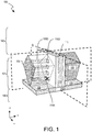
- FIG. 1 illustrates a double-sided IC structure 100 that includes GAA transistor structure 101 having a plurality of stacked channel regions 115A-115D following back-side channel depopulation in accordance with some embodiments where bottom channel region 115A has been removed (and replaced with placeholder material), or otherwise deactivated, as represented by an "X".
- Transistor structure 101 therefore includes only three active channel regions even though transistor structure 101 has a design maximum of four channel regions. Where other transistors of a double-side IC structure include the design maximum channel regions, the illustrated backside depopulation may differentiate operational parameters of two transistors.
- all transistors of a double-side IC structure 100 may also be depopulated substantially as transistor structure 101, for example to electrically isolate the transistor structures from an underlying feature, such as a sub-channel material, or backside metallization feature, etc.
- double-sided IC structure 100 includes one or more front-side metallization levels 180 over a "top” or “front” side of transistor structure 101, and one or more back-side metallization levels 190 over (under) a "bottom” or “back” side of transistor structure 101. Structural aspects of front-side metallization levels 180 and back-side metallization levels 190 are not depicted in FIG 1 to avoid obscuring the view of transistor structure 101. Front-side metallization levels 180 may have any known structure, and any number of levels interconnecting one or more transistor terminals with other nodes in a circuit.
- back-side metallization levels 190 may have any known structure, and any number of levels interconnecting one or more transistor terminals with other nodes in the circuit.
- there are more levels e.g., 6-8, or more
- front-side metallization levels 180 may be readily distinguished from back-side metallization levels 190 even where double-side IC structure 100 is inverted from the orientation illustrated.
- depopulated/inactivated channel region 115A is nearest to back-side metallization levels 190, and is therefore referred as a "bottom,” or “lower,” channel region.
- channel region 115D is nearest front-side metallization levels 180 and may therefore be referred to as a "top,” or "upper,” channel region.
- Plane A is a "gate-cut” plane that passes through a transverse length of gate electrode 110 and passes through a longitudinal length of channel regions 115A-115D.
- Plane B is a "fin-cut” plane that passes through a transverse length of channel regions 115A-115D and passes through a longitudinal length of gate electrode 110.
- source and drain regions 105 are electrically and physically coupled to opposite sides of channel regions 115A-115D.
- source and drain regions 105 comprise faceted epitaxial material that has been grown, for example laterally from an end portion of channel regions 115A-115D embedded with in a spacer dielectric material 111, or from cantilevered source/drain nanowire ends (e.g., 105D) drawn in dashed line.
- Source and drain regions 105 need not be epitaxial material, in which case the illustrated facets may not be present. Source and drain regions 105 also need not be merged into a unitary body, in which case cantilevered source/drain nanowire ends (e.g., 105D) may be individually contacted by a terminal contact metal.
- back-side metallization levels 190 include a back-side source and drain metallization 108 that is in contact with source and drain regions 105.
- front-side metallization levels 180 may include a front-side source and/or drain contact that is similarly in contact with one or more of source and drain regions 105.
- front-side metallization levels 180 and/or back-side metallization levels 190 may further include a contact to gate electrode 110 (not depicted).
- Gate electrode 110 is between source and drain region 105, with intervening spacer dielectric material 111 between gate electrode 110 and source and drain region 105.
- Transistor structure 101 may further include one or more additional dielectric materials. In the illustrated example, there is a dielectric material 140 under gate electrode 110 where gate electrode 110 extends laterally beyond channel regions 115A-11D.
- FIG. 2A illustrates a cross-sectional view of double-sided IC structure 100 along the A-A' plane introduced in FIG. 1 , in accordance with some embodiments.
- FIG. 2B illustrates a second cross-sectional view of the double-side IC structure 100 along the B-B' plane introduced in FIG. 1 , in accordance with some embodiments.
- IC structure 100 includes a transistor structure 201 that lacks at least one active bottom channel region.
- Transistor structure 201 is adjacent to a transistor structure 202 that has a full complement of active channel regions.
- Transistor structure 201 is therefore an embodiment of transistor structure 101 ( FIG. 1 ) including an electrically inactive channel material 215A.
- Transistor structures 201 and 202 may be two transistors within any IC topology, for example where different transistor drive currents are advantageous.
- IC structure 100 is a CMOS structure with transistor structure 201 having a first conductivity type while transistor structure 202 has a second, complementary conductivity type.
- transistor structure 201 is a PMOS transistor structure with source and drain region 105 having p-type conductivity
- transistor structure 202 is a NMOS transistor structure with source and drain region 106 having n-type conductivity.
- transistor structure 201 is an NMOS transistor structure with source and drain region 105 having n-type conductivity
- transistor structure 202 is a PMOS transistor structure with source and drain region 106 having p-type conductivity.
- transistor structures 201 and 202 are both PMOS transistor structures or both NMOS transistor structures.
- Source and drain region 105, 106 is coupled together through channel regions 115B, 115C and 115D.
- Each of channel regions 115B-115D are operable to contribute to a total drive current for transistor structures 201, 202.
- Transistor structure 202 includes a bottom channel region 115A that is absent from transistor structure 201, and which increases the drive current of transistor structure 202 beyond that of transistor structure 201.
- transistor structure 202 therefore has four channel regions whereas transistor structure 201sp has only three channel regions with an inactive channel material 215A in place of bottom channel region 115A. As shown in FIG. 2A , inactive channel material 215A is co-planar with bottom channel region 115A along a plane C demarked in dashed line.
- Transistor structures 201 and 202 may alternatively include any number of channel regions 115. Also, while transistor structure 201 is illustrated as lacking bottom channel region 115A, transistor structure 201 may lack any number channel regions relative to a transistor having a design maximum number of channel regions, such as transistor structure 202. For embodiments where more than one channel region is rendered inactive, two or more of the lowest channel regions, nearest back-side metallization levels 190, may be absent with inactive channel material 215 then being coplanar with one or more of channel regions 115B-115C, for example.
- Source/drain semiconductor region 105 and source/drain semiconductor region 106 may comprise any semiconductor material suitable for a transistor.
- source/drain semiconductor regions 105, 106 include impurity-doped portions of semiconductor material portions 105A-105D protruding laterally beyond channel regions 115A-115D, and denoted by dashed lines.
- source/drain regions 105, 106 include a unified epitaxial semiconductor source/drain structure. This unified epitaxial semiconductor source/drain structure may have been grown, for example, from semiconductor material portions 105A-105D that were cantilevered beyond spacer dielectric material 111.
- Source/drain region 105, 106 may be comprise one or more electrically active impurities.
- source/drain region 105 is a Group IV semiconductor material (e.g., Si, Ge, or SiGe alloy) with a p-type impurity, such as, but not limited to, boron or gallium.
- source/drain region 106 is also a Group IV semiconductor material, but with an n-type impurity, such as, but not limited to, phosphorus, arsenic, or antimony.
- Channel regions 115B-115D have a longitudinal channel length LC (e.g., along y-axis) associated with a distance between source and drain region 105 in transistor structure 201.
- Channel regions 115B-115D may extend through dielectric (spacer) material 111, as illustrated, or not.
- inactive channel material 215A also has length between source and drain region 105 that is substantially equal to channel length LC.
- inactive channel material 215A may have a longitudinal length significantly less than the channel length LC, for example where only some portion of channel length LC is electrically inactive material.
- Transistor structure 202 similarly includes channel regions 115A-115D having a longitudinal channel length (e.g., along y-axis) associated with a distance between source and drain region 106.
- Channel regions 115A-115D are non-planar bodies of semiconductor material that may have been patterned from a fin in a front (top) side of a substrate material layer, for example.
- the trapezoidal profiles illustrated for both gate electrode 110 and channel regions 115A-115D are representative of structural asymmetry associated with front-side transistor fabrication. Such asymmetry may be a result of feature sidewall slopes that evolve during subtractive patterning of one or more of a semiconductor fin or gate electrode.
- channel regions 115A-115D are illustrated in FIG. 2B as nanowires having a transverse width approximately equal to their vertical thickness, channel regions 115A-115D may instead be nanoribbons.
- channel regions 115A-115D are crystalline semiconductor.
- the crystalline semiconductor includes polycrystalline thin film material, the crystalline semiconductor may be advantageously substantially monocrystalline.
- the crystallinity of channel regions 115A-115D is cubic with the top surfaces nearest to front-side metallization levels 180 having crystallographic orientation of (100), (111), or (110), for example. Other crystallographic orientations are also possible.
- channel regions 115A-115D are a substantially monocrystalline group IV semiconductor material, such as, but not limited to substantially pure silicon (e.g., having only trace impurities), silicon alloys (e.g., SiGe), germanium alloys (e.g., GeSn, SiGeSn) or substantially pure germanium (e.g., having only trace impurities).
- channel regions 115A-115D are a Group III-V alloy semiconductor material. Channel regions 115A-115D may also have any of these same exemplary compositions in alternative polycrystalline or amorphous embodiments, for example where transistor structures 201, 202 have been fabricated from a thin film semiconductor material layer.
- Alternative polycrystalline or amorphous embodiments may instead include semiconducting metal oxides, such as IGZO.
- channel regions 115A-115D are illustrated as having a substantially homogenous composition, they may alternatively comprise one or more semiconductor heterojunctions that, for example further include a first semiconductor material adjacent to a second semiconductor material.
- Inactive channel material 215A is compositionally different from channel regions 115A-115D.
- Inactive channel material 215A may be any material that is inoperable as a channel material, at least under the gate bias voltages at which channel regions 115A-115D are operable and/or to which transistor structure 201 is biased during circuit operation.
- inactive channel material 215A is a dielectric material. Suitable dielectric materials include, but are not limited to, silicon dioxide, a low-k dielectric (e.g., SiOC), silicon oxynitride, silicon nitride, or an even high-k dielectric (e.g., metal oxide).
- transistor structures 201 and 202 have substantially the same gate electrode height H1.
- transistor structure 202 includes a sub-channel material 200 extending a height H2 from a nearest one of back-side metallization levels 190.
- Sub-channel material 200 is under the stack of channel regions 115A-115D, under gate electrode 110, and may be a base of a fin, for example, from which channel regions 115A-115D were formed.
- sub-channel material 200 may have a composition and/or microstructure similar to channel regions 115-115D.
- sub-channel material 200 is also a Group IV material (e.g., silicon).
- sub-channel material 200 is also substantially monocrystalline, and has the same crystallinity and/or crystal orientation as that of channel regions 115A-115D.
- transistor structure 201 In addition to lacking channel region 115A, transistor structure 201 also lacks sub-channel material 200. As shown, inactive channel material 215A is in place of both sub-channel material 200 and channel region 115A, having a height H3 from back-side metallization levels 190. In other words, inactive channel material 215A is coplanar with both sub-channel material 200 and channel region 115A. In the illustrated example, within transistor structure 201, inactive channel material 215A also occupies a region where a bottom portion of the gate stack resides within transistor structure 202. As such, for transistor structure 201, spacing between a given one of back-side interconnect metallization levels 190 and a nearest one of channel regions 115B-115D is greater than height H3. In contrast, for transistor structure 202, spacing between the given one of back-side interconnect metallization levels 190 and a nearest one of channel regions 115A-115D is less than height H3.
- transistor structure 201 may have been modified from a transistor structure that was substantially the same as transistor structure 202 through selective back-side processing that has removed sub-channel material 200, as well as channel region 115A, and replaced it with inactive channel material 215A.
- channel regions 115B-115D of transistor structure 201 remain advantageously unaltered from their counterpart regions of transistor structure 202, which is one of the advantages of back-side channel depopulation in accordance with embodiments herein.
- transistor structures 201 and 202 include a gate stack further including gate electrode 110 and a gate dielectric 217 cladding channel regions 115-115D to provide gate-all-around control of channel conductivity.
- Gate dielectric 217 may be any dielectric material(s) known to be suitable as an insulator of a gate electrode, such as, but not limited to SiO2, SiONx.
- gate dielectric 217 includes a high-k material (with a bulk relative permittivity greater than 8).
- Exemplary high-k materials include metal oxides, such as, but not limited to a metal oxide comprising predominantly aluminum (e.g., Al2O3), a metal oxide comprising predominantly magnesium (e.g., MgO), a metal oxide comprising predominantly lanthanum (e.g., La2O3), a metal oxide comprising predominantly hafnium (e.g., HfO2), or an alloy metal oxide comprising significant portions of two or more of these metals (e.g., HfAlOx).
- the high-k material further includes silicon.
- metal silicates such as, but not limited to HfSiOx, or TaSiOx may also be suitable for some semiconductor compositions (e.g., Si, Ge, SiGe, III-V).
- high-k gate dielectric materials include, for instance, hafnium oxide, hafnium silicon oxide, lanthanum oxide, lanthanum aluminum oxide, zirconium oxide, zirconium silicon oxide, tantalum oxide, titanium oxide, barium strontium titanium oxide, barium titanium oxide, strontium titanium oxide, yttrium oxide, aluminum oxide, lead scandium tantalum oxide, and lead zinc niobate.
- the gate electrode 110 is shown as a single monolithic layer.
- gate electrode 110 may comprise a workfunction metal over the gate dielectric 217, and a compositionally distinct fill metal.
- An n-type workfunction metal may have a workfunction between about 3.9 eV and about 4.2 eV, for example.
- Suitable n-type work function metals include, but are not limited to, hafnium, zirconium, titanium, tantalum, aluminum, and metal carbides that include these elements (e.g., titanium carbide, zirconium carbide, tantalum carbide, hafnium carbide and aluminum carbide).
- a p-type workfunction metal may have a workfunction between about 4.9 eV and about 5.2 eV, for example.
- Suitable p-type materials include, but are not limited to, ruthenium, palladium, platinum, cobalt, nickel, and conductive metal oxides (e.g., ruthenium oxide).
- FIG. 3A illustrates a cross-sectional view of double-sided IC structure 100 along the A-A' plane introduced in FIG. 1 , in accordance with some alternative embodiments.
- FIG. 3B illustrates a second cross-sectional view of the double-side IC structure 100 along the B-B' plane introduced in FIG. 1 , in accordance with the alternative embodiments.
- IC structure 100 includes a transistor structure 301 that lacks at least one active bottom channel region.
- Transistor structure 301 is again adjacent to transistor structure 202 that has the full complement of active channel regions.
- Transistor structure 301 is therefore an alternative embodiment of transistor structure 101 ( FIG. 1 ) that includes an electrically inactive channel material 315A.
- Transistor structures 301 and 201 may be two transistors within any IC topology, for example where different transistor drive currents are advantageous.
- IC structure 100 is a CMOS structure with transistor structure 301 having a first conductivity type while transistor structure 202 has a second, complementary conductivity type.
- transistor structure 301 is a PMOS transistor structure with source and drain region 105 again having p-type conductivity
- transistor structure 202 is an NMOS transistor structure with source and drain region 106 again having n-type conductivity.
- transistor structure 301 is an NMOS transistor structure with source and drain region 105 having n-type conductivity
- transistor structure 202 is a PMOS transistor structure with source and drain region 106 having p-type conductivity
- transistor structures 301 and 202 are both PMOS transistor structures or both NMOS transistor structures.
- Transistor structures 301 share many of the structural elements described above for transistor structures 201 and 202.
- the reference numbers introduced in FIG. 2A and 2B are retained in FIG. 3A and 3B for structural features in transistor structures 301 that have a direct analog in transistor structures 201 and 202.
- transistor structure 301 lacks a bottom channel region 115A, however there is an inactive channel material 315A that has been derived from the channel region material.
- inactive channel material 315A may have a less dramatically different composition and/or microstructure than channel regions 115A-115D.
- inactive channel material 315A is also substantially monocrystalline, and has the same crystallinity and/or crystal orientation as that of channel regions 115B-115D.
- inactive channel material 315A has a greater concentration of impurities that render inactive channel material 315A inoperable as a channel material, at least under the gate bias voltages at which channel regions 115A-115D are operable. Except for the greater impurity concentration, inactive channel material 315A may be substantially the same material as channel regions 115B-115D.
- inactive channel material 315A may also be the Group IV semiconductor material, but impurity doped to have a threshold voltage that renders inactive channel material 315A in an "off state under all gate bias voltages that transistor structure 301 may experience during circuit operation.
- inactive channel material 315A includes an electrically active impurity that results in inactive channel material 315A having a conductivity type complementary to source/drain region 105.
- inactive channel material 315A may be n-type. Complementary doping may provide junction isolation with source and drain region 105.
- Suitable impurities for an n-type inactive silicon channel material 315A of a PMOS device include, but are not limited to, phosphorus, arsenic, or antimony.
- P-type inactive channel material 315A is also possible.
- suitable impurities for an inactive p-type silicon channel material 315A include, but are not limited to, boron or gallium or indium.
- inactive channel material 315A has an impurity concentration in excess of 1e19 atoms/cm3 (e.g., approximately 1e20 atoms/cm3, or more).
- substantially the entire channel length LC is impurity doped into inactive channel material 315A.
- a co-planar portion of source/drain regions 105 e.g., along plane C in FIG. 3A
- a longitudinal length significantly less than channel length LC may be impurity doped into inactive channel material 315A.
- the longitudinal length of inactive channel material 315A should however at least be sufficient to avoid significant source-to-drain leakage through inactive channel material 315A.
- transistor structure 301 includes sub-channel material 200 extending a height H2 from back-side metallization levels 190.
- sub-channel material 200 may be a base of a fin, for example, from which inactive channel material 315A and channel regions 115B-115D were formed.
- sub-channel material 200 may have a composition and/or microstructure similar to channel regions 115B-115D.
- channel regions 115B-115D are of a Group IV material (e.g., silicon)
- sub-channel material 200 is also a Group IV material (e.g., silicon).
- sub-channel material 200 is also substantially monocrystalline, and has the same crystallinity and/or crystal orientation as that of channel regions 115B-115D.
- a significant impurity concentration may be advantageously limited to inactive channel material 315A with channel region 115B remaining operable with an associated threshold voltage.
- the concentration of the impurity present in inactive channel material 315A is at least two orders of magnitude lower within channel regions 115B-115D, and may be advantageously three orders of magnitude, or more.
- channel regions 115B-115D (as well as channel region 115A of transistor structure 202) may be substantially undoped by the impurity present within inactive channel material 315A.
- a steep impurity gradient along the height H3 may therefore be present within transistor structure 301 with no such impurity along the height H3 in transistor structure 202.
- Sub-channel material 200 may, in contrast, be doped with the impurity present within inactive channel material 315A.
- the inactive channel material impurity is complementary to impurities in source/drain region 105
- inclusion of a significant impurity concentration within sub-channel material 200 may also improve electrical isolation of sub-channel material 200.
- Sub-channel material 200 may alternatively have a significantly lower concentration of the impurity found in inactive channel material 315A.
- inactive channel material 315A has a lower degree of crystallinity that channel regions 115B-115D. Lesser long range order within inactive channel material 315A may help to confine impurities to within the inactive channel material 315A, increasing the impurity gradient along the height H3.
- inactive channel material 315A may include one or more amorphizing impurities, such as silicon or germanium or argon or xenon or krypton or tin.
- amorphizing impurities such as silicon or germanium or argon or xenon or krypton or tin.
- the presence of germanium within inactive channel material 315A is indicative of a targeted amorphization.
- channel regions 115B-115D comprise predominantly germanium
- the presence of silicon within inactive channel material 315A is likewise indicative of a targeted amorphization.
- Such impurities within a majority Group IV semiconductor may impart significant lattice damage that reduces the crystallinity of inactive channel material 315A below that of channel regions 115B-115D.
- sub-channel material 200 may also incur some lesser degree of lattice damage and may also comprise some lower concentration of the one or more amorphizing impurities found at a higher concentration within inactive channel material 315A.
- Amorphizing impurities are advantageously substantially absent from channel regions 115B-115D (as well as 115A in transistor structure 202). So, in addition to greater crystallinity, channel regions 115B-115D may have a much lower amorphizing impurity concentration than inactive channel material 315A.
- transistor structure 301 may have been modified from a transistor structure that was substantially the same as transistor structure 202 through selective back-side implantation of impurities (electrically active or amorphizing) into channel region 115A, converting it into inactive channel material 315A.
- channel regions 115B-115D of transistor structure 201 remain advantageously unaltered from their counterpart regions of transistor structure 202.
- a lack of crystal damage (i.e., high degree of crystallinity) and low (e.g., intrinsic levels) of impurities within channel regions 115B-115D are indicative of back-side channel depopulation in accordance with embodiments herein.
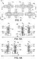
- FIG. 4 is a plan view layout of a six-transistor (6-T) SRAM cell that includes multiple transistor structures, at least one of the transistor structures including a first number active channel regions, and at least a second of the transistor structures including a second number of active channel regions, in accordance with some embodiments.
- 6-T six-transistor
- SRAM cell 401 a plurality of channel regions 115 and gate electrodes 110 are interconnected by both front-side and back-side metallization levels (not depicted).
- SRAM cell 401 comprises a pair of PMOS pull-up transistors (PU1 and PU2), a pair of NMOS pass-gate transistors (PG1 and PG2), and a pair of NMOS pull-down transistors (PD1 and PD2).
- PU1 and PU2 transistors have the transistor structure 201 or 301 while PG1 and PG2 and PD1 and PD2 all have transistor structure 202.
- the drive strength of the PU transistors will be less than that of the PD and PG transistors.
- better balance between the read stability and write-ability may be provided, potentially eliminating the need for assist circuits, and reducing IC area and/or IC power consumption.
- FIG. 5A is a cross-sectional view through a first plurality of transistors in the 6-T SRAM cell 401 along the B1-B1' line, in accordance with some embodiments.
- FIG. 5B is a cross-sectional view through a second plurality of transistors in the 6-T SRAM cell 401 along the B2-B2' line, in accordance with some embodiments.
- the PG1, PG2, PD1, and PD2 transistors each have the design maximum number (e.g., four) of channel regions (e.g., 115A-115D).
- the PU1 and PU2 transistors each have an inactive channel material 215A and less than the design maximum number of channel regions (e.g., only three channel regions 115B-115D).
- PU1 and PU2 transistors each instead have at least one inactive channel material 315A, for example having the transistor structure 301 rather than transistor structure 201.
- FIG. 6 is a flow diagram illustrating methods 600 for depopulating one or more bottom channel regions of a RoW transistor structure, in accordance with some embodiments.
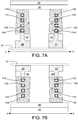
- FIG. 7A-7F illustrate cross-sectional views of two transistor structures in a double-side IC structure evolving during the practice of methods 600 to provide a different number of channel regions in transistor structures 201 and 202 ( FIG. 2A-2B ).
- methods 600 begin at input 605 where an IC workpiece with a ribbon or wire (RoW) transistor structures is received.
- the IC workpiece includes a plurality of RoW transistor structures over an area of substrate, such as a semiconductor wafer, that is to become in IC chip.
- the IC workpiece may be substantially complete through both a front-end-of-line process (FEOL) where the transistor structures were fabricated, and a back-end-of-line process (BEOL) where front-side metallization levels interconnecting the transistor structures have been completed.
- FEOL front-end-of-line process
- BEOL back-end-of-line process
- a front side of the IC workpiece is bonded, at least temporarily, to a handle or host substrate.
- Any bonding technique e.g., wafer-level
- a suitable host substrate 702 has been bonded to an uppermost material layer of front-side metallization levels 180.
- Front-side metallization levels 180 is illustrated in dashed line to emphasize front-side metallization levels 180 may include any number of BEOL interconnect metallization levels.
- the composite IC workpiece may be inverted, as further illustrated in FIG. 7B , to subject a back-side of a donor substrate 701 to back-side processing.
- FIG. 7C further illustrates an example where at least a portion of a donor substrate 701 has been removed exposing a back-side of sub-channel material 200. Removal of donor substrate 701 may entail a polish (e.g., CMP) and/or a wet or dry (e.g., plasma) etch process. Any grind, polish, and/or wet/dry etch process known to be suitable for the composition of the donor substrate 701 may be employed.
- a polish e.g., CMP
- a wet or dry (e.g., plasma) etch process e.g., any grind, polish, and/or wet/dry etch process known to be suitable for the composition of the donor substrate 701 may be employed.
- the carrier layer is a group IV semiconductor (e.g., silicon)
- a CMP slurry known to be suitable for thinning the semiconductor may be employed.
- any wet etchant or plasma etch process known to be suitable for thinning the group IV semiconductor may also be employed.
- removal of donor substrate 701 entails a cleaving or fracture process that removes a substantial portion of the donor substrate thickness, reducing the polish or etch time required.
- donor substrate 701 is 400-900 ⁇ m of, for example, silicon, 100-700 ⁇ m may be cleaved off by practicing any blanket implant known to promote a wafer-level fracture.
- a light element e.g., H, He, or Li
- Donor substrate material removal may be continued until an endpoint criteria is met. As further illustrated in FIG. 7C , for example, donor substrate material removal may be terminated upon exposing dielectric material 140, which surrounds some portion of sub-channel material 200.
- methods 600 continue to block 630 where a bottom number of channel regions are removed with one or more etch process suitable for the materials encountered during a back-side recess etch.
- a back-side etch process selective to sub-channel material 200 has been employed to form a recess 730 that exposed a back side of gate electrode 110.
- Recess 730 is further advanced through a back-side (bottom) thickness of gate electrode 110, for example with another etch process that is selective to the composition of gate electrode 110.
- Recess 730 is further advanced through a back-side (bottom) thickness of gate dielectric 217, which exposes a back-side of channel region 115A illustrated in dash line.
- Channel region 115A is also etched away, for example with any etch process (wet chemical or dry plasma) suitable for the composition of channel region 115A (e.g., silicon, SiGe, Ge, etc.). With channel region 115A removed, advancement of recess 730 may halted, or continued to remove one or more additional channel regions 115B-115D, to complete block 630 ( FIG. 6 ). Notably, in the illustrated example the backside recess etching is substantially self-aligned, requiring only an etch mask that protects adjacent transistor structures that are to retain the design maximum number of channel regions.
- any etch process wet chemical or dry plasma
- Methods 600 continue to block 640 where the recess formed at block 630 is backfilled with a material that will be electrically inactive.
- the channel regions removed from a transistor structure at block 630 are replaced with a dielectric material.
- electrically inactive channel material 215A is deposited into recess 730. Any suitable deposition process and/or planarization process may be employed to at least partially backfill recess 730.
- methods 600 end at output 650 where a back-side interconnect metallization levels of the IC workpiece are completed. Any other back-side processing may also be completed to arrive at a final double-side IC structure.
- back-side source/drain contact metallization 108 is formed as a first of one or more back-side metallization levels 190.
- back-side source/drain contact metallization 108 entails an (e.g., unmasked, self-aligned) etch of dielectric material 140 with an etchant that is selective to the composition of dielectric material 140 relative to that of inactive channel material 215A. Any metal deposition process and planarization process may then be practiced to arrive at the transistor structures 201 and 202.
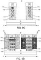
- FIG. 8 is a flow diagram illustrating methods 800 for depopulating one or more bottom channel regions of a RoW transistor structure, in accordance with some alternative embodiments relying on ion implantation from a back side of an IC workpiece.
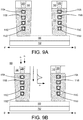
- FIG. 9A-9D illustrate cross-sectional views of two transistor structures in a double-side IC structure evolving during the practice of methods 800 to provide a different number of active bottom channel regions in transistor structures 301 and 202 ( FIG. 3A-3B ).
- the IC workpiece includes a plurality of RoW transistor structures over an area of substrate, such as a semiconductor wafer, that is to become in IC chip.
- the IC workpiece may be substantially complete through both a front-end-of-line process (FEOL) where the transistor structures were fabricated, and a back-end-of-line process (BEOL) where front-side metallization levels interconnecting the transistor structures have been completed.
- FEOL front-end-of-line process
- BEOL back-end-of-line process
- a front side of the IC workpiece is bonded, at least temporarily, to a host or handle substrate.
- Any bonding technique e.g., wafer-level
- Methods 800 continue at block 620 where the host substrate is removed to reveal a back side of transistor structures within the IC workpiece, for example substantially as described above, to arrive at the exemplary structure further illustrated in FIG. 9A .
- methods 800 proceed to block 830 where one or more ion implantations are performed to implant one or more impurities into a number of transistor channel regions.
- a pre-amorphization implant is performed from the back side of the IC workpiece so that the species is implanted through a depth of the transistor to come to rest within one or more of the lower channel regions that are to be electrically deactivated.
- one or more impurities that can be eclectically activated may be similarly implanted from the back side of the IC workpiece so that the impurity similarly comes to rest within one or more of the lower channel regions that are to be electrically deactivated. In the example further illustrated in FIG.
- an n-type impurity (n-) is illustrated as being implanted to achieve a concentration profile qualitatively represented as peaking at a plane of channel region 115A within one of the transistor structures.
- An amorphization species concentration may be implanted to achieve a similar impurity concentration profile.
- a pre-amorphization species is implanted into the transistor structure, through any sub-channel material exposed on the back side.
- Species implantation may be with an incident angle that is substantially normal to a back-side surface of the transistor structures (i.e., with no tilt).
- the pre-amorphization and/or electrically active dopant species will only enter the channel regions through the bottom channel region 115A.
- the energy of the implantation process may be chosen to isolate the majority of the pre-amorphization and/or electrically active dopant species within the bottom channel region 115A.
- an implantation energy of a silicon or germanium pre-amorphization species may be between approximately IkeV and approximately 2keV.
- Such an implant may induce a change in crystallinity of channel region 115A.
- additional channel regions 115B-115D may also be altered to amorphize more than one channel region.
- Implanted dopants that can be electrically activated similarly only enter the stack through the back side, encountering a desired number of bottom channel regions.
- a secondary implant may be subsequently performed without an annealing process between the two implant processes. As such, the disrupted crystal structure of channel region 115A is maintained and the n-species concentration profile may be made more peaked to ensure channel region 115B may remain active.
- the n- impurity is implanted with an energy in the range of 1-2keV.
- a higher energy may be employed to increase impurity concentrations deeper into the IC workpiece, for example within an additional number of channel regions (e.g., 115B-115D).
- sub-channel material 200 may also be impurity doped by the back-side implantation employed to deactivate one or more channel regions.
- the only mask required during the backside implantation process(es) is one which protects various adjacent structures that are to retain a full complement of channel regions.
- a short (flash) activation anneal may be performed to electrically active some percentage of the impurities implanted into channel region 115A sufficient to render it inactive channel material 315A, as illustrated in FIG. 9C .
- methods 800 complete at output 650 where back-side interconnect metallization levels of the IC workpiece are completed. Any other back-side processing may also be completed to arrive at a final double-side IC structure.
- back-side source/drain contact metallization 108 has been formed as a first of one or more back-side metallization levels 190.
- formation of back-side source/drain contact metallization 108 entails an (unmasked, self-aligned) etch of dielectric material 140 with an etchant that is selective to the composition of dielectric material 140 relative to that of inactive channel material 315A (e.g., selective to n-type silicon). Any metal deposition process and planarization process may then be practiced to arrive at the transistor structures 301 and 202 substantially as described above.
- FIG. 10 is a cross-sectional view of a double-sided IC structure 1000, in accordance with some embodiments.
- Double-sided IC structure 1000 illustrates a portion of a monolithic IC that includes FEOL interconnect metallization levels 180 over and/or on a front side of transistor structures 1001 that include RoW transistor structures, one or more of which have been depopulated of one or more lower (back-side) channel regions.
- front-side interconnect metallization levels 180 include interconnect metallization 1025 electrically insulated by dielectric material 1026.
- front-side interconnect metallization levels 180 includes metal-one (M1), metal-two (M2), metal-three (M3) and metal-n (Mn) interconnect metallization levels.
- Interconnect metallization 1025 may be any metal(s) suitable for IC interconnection.
- Interconnect metallization 1025 may be, for example, an alloy of predominantly Cu, an alloy of predominantly W, an alloy of predominantly Ru, an alloy of predominantly Al, an alloy of predominantly Mo, etc.
- Dielectric material 1026 may be any dielectric material known to be suitable for electrical isolation of monolithic ICs.
- dielectric material 1026 comprises silicon, and at least one of oxygen and nitrogen.
- Dielectric material 1026 may be SiO, SiN, or SiON, for example.
- Dielectric material 1026 may also be a low-K dielectric material (e.g., having a dielectric constant below that of SiO2).
- Double-sided IC structure 1000 further includes back-side interconnect metallization levels 190.
- interconnect metallization levels 190 interconnect metallization 1025 is again electrically insulated by dielectric material 1026.
- Back-side metallization levels 190 may comprise any number of metallization levels over, or on, a back side of transistor structures 1001.
- back-side metallization levels 190 include a metallization level M1' through nearest to transistor structures 1001 (e.g., opposite M1) through an uppermost back-side metallization level Mn'.
- IC structure 1000 includes one level of transistor structures 1001, there may be multiple levels of transistor structures located within the various interconnect metallization levels, for example where a front-side metallization level of one IC structure has been bonded to a back-side metallization level of another IC structure to arrive at a composite 3DIC.
- transistor structures 1001 includes one or more PMOS GAA transistor structures having a smaller number of channel regions than one or more NMOS GAA transistor structures.
- one or more NMOS GAA transistor structures have a smaller number of channel regions than one or more PMOS GAA transistor structures.
- one or more first PMOS GAA transistor structures have a smaller number of channel regions than one or more second PMOS GAA transistor structures.
- one or more first NMOS GAA transistor structures have a smaller number of channel regions than one or more second NMOS GAA transistor structures.
- one or more lower channel regions may have been depopulated according to any of the back-side techniques described herein to arrive at any of the structures described elsewhere herein.
- FIG. 11 illustrates a system in which a mobile computing platform 1105 and/or a data server machine 1106 employs an IC with including a double-sided memory and/or microprocessor IC with depopulated RoW transistor structures, for example in accordance with some embodiments described elsewhere herein.
- the server machine 1106 may be any commercial server, for example including any number of high-performance computing platforms within a rack and networked together for electronic data processing, which in the exemplary embodiment includes a monolithic IC 1150.
- the mobile computing platform 1105 may be any portable device configured for each of electronic data display, electronic data processing, wireless electronic data transmission, or the like.
- the mobile computing platform 1105 may be any of a tablet, a smart phone, laptop computer, etc., and may include a display screen (e.g., a capacitive, inductive, resistive, or optical touchscreen), a chip-level integrated system 1110, and a battery 1115.
- IC 1150 may include memory circuitry (e.g., RAM), and/or a logic circuitry (e.g., a microprocessor, a multi-core microprocessor, graphics processor, or the like) at least one of which further includes one or more back-side depopulated RoW transistor structures, for example in accordance with some embodiments described elsewhere herein.
- IC 1150 may be further coupled to a board, a substrate, or an interposer 1160 that further hosts one or more additional ICs, such as power management IC 1130 and radio frequency IC 1125.
- RFIC 1125 may have an output coupled to an antenna (not shown) to implement any of a number of wireless standards or protocols, including but not limited to Wi-Fi (IEEE 802.11 family), WiMAX (IEEE 802.16 family), IEEE 802.20, long term evolution (LTE), Ev-DO, HSPA+, HSDPA+, HSUPA+, EDGE, GSM, GPRS, CDMA, TDMA, DECT, Bluetooth, derivatives thereof, as well as any other wireless protocols that are designated as 3G, 4G, 5G, and beyond.
- FIG. 12 is a functional block diagram of an electronic computing device 1200, in accordance with some embodiments.
- Device 1200 further includes a motherboard 1202 hosting a number of components, such as, but not limited to, a processor 1204 (e.g., an applications processor).
- processor 1204 may be physically and/or electrically coupled to motherboard 1202.
- processor 1204 is part of a monolithic IC structure including one or more back-side depopulated RoW transistor structures, as described elsewhere herein.
- the term "processor” or “microprocessor” may refer to any device or portion of a device that processes electronic data from registers and/or memory to transform that electronic data into other electronic data that may be further stored in registers and/or memory.
- one or more communication chips 1206 may also be physically and/or electrically coupled to the motherboard 1202. In further implementations, communication chips 1206 may be part of processor 1204. Depending on its applications, computing device 1200 may include other components that may or may not be physically and electrically coupled to motherboard 1202.
- volatile memory e.g., DRAM 1232
- non-volatile memory e.g., ROM 1235
- flash memory e.g., NAND or NOR
- magnetic memory MRAM 1230
- graphics processor 1222 e.g., a digital signal processor, a crypto processor, a chipset 1212, an antenna 1225, touchscreen display 1215, touchscreen controller 1265, battery 1216, audio codec, video codec, power amplifier 1221, global positioning system (GPS) device 1240, compass 1245, accelerometer, gyroscope, speaker 1220, camera 1241, and mass storage device (such as hard disk drive, solid-state drive (SSD), compact disk (CD), digital versatile disk (DVD), and so forth, or the like.
- volatile memory e.g., DRAM 1232
- non-volatile memory e.g., ROM 1235
- flash memory e.g., NAND or NOR
- MRAM 1230 magnetic memory
- graphics processor 1222 e.
- Communication chips 1206 may enable wireless communications for the transfer of data to and from the computing device 1200.
- the term "wireless” and its derivatives may be used to describe circuits, devices, systems, methods, techniques, communications channels, etc., that may communicate data through the use of modulated electromagnetic radiation through a non-solid medium. The term does not imply that the associated devices do not contain any wires, although in some embodiments they might not.
- Communication chips 1206 may implement any of a number of wireless standards or protocols, including, but not limited to, those described elsewhere herein.
- computing device 1200 may include a plurality of communication chips 1206.
- a first communication chip may be dedicated to shorter-range wireless communications, such as Wi-Fi and Bluetooth, and a second communication chip may be dedicated to longer-range wireless communications such as GPS, EDGE, GPRS, CDMA, WiMAX, LTE, Ev-DO, and others.
- an integrated circuit (IC) structure comprises a first interconnect metallization level, a second interconnect metallization level, and first and second transistor structures between the first interconnect metallization level and the second interconnect metallization level.
- the first transistor structure comprises a first gate electrode around a stack of a first number of channel regions.
- the second transistor structure comprises a second gate electrode around a stack of a second number of channel regions, greater than the first number of channel regions.
- a first spacing between the second interconnect metallization level and a nearest one of the first number of channel regions is greater than a second spacing between the second interconnect metallization level and a nearest one of the second number of channel regions.
- the first transistor structure further comprises a first source region coupled to a first drain region through the first number of channel regions, and the first source region and the first drain region have a first conductivity type.
- the second transistor structure further comprises a second source region coupled to a second drain region through the second number of channel regions, the second source region and the second drain region have a second conductivity type, complementary to the first conductivity type.
- an IC structure further comprises an inactive semiconductor material between the nearest one of the first number of channel regions and the second interconnect metallization level.
- the inactive semiconductor material is substantially coplanar with the nearest one of the second number of channel regions, and the inactive semiconductor material has the second conductivity type with an impurity concentration exceeding that in the first number of channel regions.
- the first channel regions have a first channel length between the first source and the first drain, and the inactive semiconductor material also has the first channel length.
- the first transistor structure is a PMOS transistor structure and the first conductivity type is p-type.
- the second transistor structure is an NMOS transistor structure and the second conductivity type is n-type.
- the impurity comprises at least one of P, Ar, or Sb, and the impurity concentration is at least 1e19cm-3.
- the IC structure further comprises a monocrystalline material between the second interconnect metallization level and the nearest one of the first number of channel regions.
- the monocrystalline material is also between the second interconnect metallization level and the nearest one of the second number of channel regions.
- the monocrystalline material has a lower concentration of the impurity than the inactivated semiconductor material.
- the IC structure further comprises a dielectric material between the nearest one of the first number of channel regions and the second interconnect metallization level.
- the dielectric material is substantially coplanar with the nearest one of the second number of channel regions.
- the dielectric material is between a portion of the first source region and a portion of the first drain region.
- the first number of channel regions have a first channel length
- the dielectric material has at least the first channel length
- the second metallization level is coupled to at least one of the first source region or the first drain region through a contact metallization located between the second metallization level and a portion of the first source or the first drain that is adjacent to the dielectric material.
- a static random access memory (SRAM) cell structure comprises a pair of pull-up transistor structures. Individual ones of the pull-up transistor structures comprise a gate electrode around individual ones of a first number of channel regions in a stack.
- the SRAM cell structure further comprises a pair of pull-down transistor structures. Individual ones of the pull-down transistor structures comprise a gate electrode around individual ones of a second number of channel regions in a stack.
- the SRAM cell structure further comprises a pair of pass-gate transistor structures. Individual ones of the pass-gate transistor structures comprise a gate electrode around individual ones of a third number of channel regions in a stack.
- the SRAM cell structure further comprises a first interconnect metallization level over a first side of the transistor structures and coupled to one or more of the pass-gate, pull-up, or pull-down transistor structures.
- the SRAM cell structure further comprises a second interconnect metallization level under a second side of the transistor structures and coupled to one or more of the pass-gate, pull-up, or pull-down transistor structures.
- the first number of channel regions is less than both the second number of channel regions and the third number of channel regions.
- a first spacing between the second interconnect metallization level and a nearest one of the first number of channel regions is greater than a second spacing between the second interconnect metallization level and a nearest one of the second number of channel regions.
- the pull-up transistor structure further comprises an inactive semiconductor material or dielectric material between a portion of a source region and a drain region further coupled to the first number of channel regions.
- the computer system comprises a power supply and an IC die coupled to the power supply, the IC die comprising the integrated circuit (IC) structure of the first through eleventh examples.
- the computer system further comprises a battery coupled to the power supply.
- a method of fabricating an IC structure comprises receiving a workpiece comprising transistor structures and front-side interconnect metallization, the transistor structures comprising a stack of a first number of channel regions.
- the method comprises exposing a back side of the transistor structures by removing or thinning a back-side substrate from the workpiece.
- the method further comprises removing or disabling one or more of the channel regions nearest to the back-side of the workpiece in at least one of the transistor structures.
- removing or disabling one or more of the channel regions comprises implanting an impurity into at least one of the transistor structures from the back side.
- the implanting is to depth that includes only one of the channel regions.
- removing or disabling one or more of the channel regions comprises exposing a first of the channel regions by etching through one or more materials from the back side of at least one of the transistor structures, and removing at least a portion of the first of the channel regions.
- the method further comprises at least partially backfilling a recess where the first of the channel regions was removed with a dielectric material.
- a computer system comprises a power supply and an IC die coupled to the power supply, the IC die comprising the integrated circuit (IC) structure of any one of the first through eleventh examples.
- the computer system further comprises a battery coupled to the power supply.
- the above embodiments are not limited in this regard and, in various implementations, the above embodiments may include the undertaking of only a subset of such features, undertaking a different order of such features, undertaking a different combination of such features, and/or undertaking additional features than those features explicitly listed.
- the scope of the invention should, therefore, be determined with reference to the appended claims, along with the full scope of equivalents to which such claims are entitled.
Landscapes
- Metal-Oxide And Bipolar Metal-Oxide Semiconductor Integrated Circuits (AREA)
Abstract
Description
- This application is related to
US16/146,800 filed on September 28, 2018 US16/827,570 filed on March 23, 2020 - Demand for higher performance integrated circuits (ICs) in electronic device applications has motivated increasingly dense transistor architectures. Fabricating interconnect metallization over both a front side of a transistor structure and over a back side of the transistor structure is a form of monolithic 3D integration where transistor structures are interconnected into a double-sided IC from both the front and back side. Such double-sided interconnect routing can reduce density and parasitics of the IC.
- Transistor structures with different drive currents may be needed for different applications within a given IC. For finFETs architectures, one may vary the number of fins between different transistor structures to achieve different drive-currents. Gate-all-around (GAA) transistor structures, such as ribbon or wire (RoW) architectures include a plurality of channel regions that are in a vertical stack with one channel region self-aligned over another. To vary the number of channel regions, one of the GAA transistor structures may be depopulated in one stack relative to the other.
- RoW depopulation techniques and double-sided transistor structures that result from such techniques may advantageously achieve different drive currents in GAA transistor structures of a double-sided IC.
- The material described herein is illustrated by way of example and not by way of limitation in the accompanying figures. For simplicity and clarity of illustration, elements illustrated in the figures are not necessarily drawn to scale. For example, the dimensions of some elements may be exaggerated relative to other elements for clarity. Further, where considered appropriate, reference labels have been repeated among the figures to indicate corresponding or analogous elements. In the figures:
-
FIG. 1 illustrates a double-sided IC structure including a gate-all-around transistor structure lacking at least one active bottom channel region following back-side channel depopulation, in accordance with some embodiments; -
FIG. 2A illustrates a first cross-sectional view of a double-side IC structure including a first transistor structure lacking at least one active bottom channel region adjacent to a second transistor structure with a full complement of active channel regions, in accordance with some embodiments; -
FIG. 2B illustrates a second cross-sectional view of the double-side IC structure illustrated inFIG. 2A , in accordance with some embodiments; -
FIG. 3A illustrates a first cross-sectional view of a double-side IC structure including a first transistor structure lacking at least one active bottom channel region adjacent to a second transistor structure with a full complement of active channel regions, in accordance with some alternative embodiments; -
FIG. 3B illustrates a second cross-sectional view of the double-side IC structure illustrated inFIG. 3A , in accordance with some alternative embodiments; -
FIG. 4 is a plan view layout of a six-transistor (6-T) SRAM cell that includes multiple transistor structures, at least one of the transistor structures including a first number active channel regions, and at least a second of the transistor structures including a second number of active channel regions, in accordance with some embodiments; -
FIG. 5A is a cross-sectional view through a first plurality of transistors in the 6-T SRAM cell illustrated inFIG. 4 , in accordance with some embodiments; -
FIG. 5B is a cross-sectional view through a second plurality of transistors in the 6-T SRAM cell illustrated inFIG. 4 , in accordance with some embodiments; -
FIG. 6 is a flow diagram illustrating methods of depopulating one or more channel regions from the back side of a RoW transistor structure, in accordance with some embodiments; -
FIG. 7A, 7B ,7C, 7D ,7E, and 7F illustrate cross-sectional views of two transistor structures in a double-side IC structure evolving to include a different number of channel regions, in accordance with some embodiments; -
FIG. 8 is a flow diagram illustrating methods of depopulating one or more channel regions from a back side of a RoW transistor structure, in accordance with some embodiments; -
FIG. 9A, 9B ,9C, and 9D illustrate cross-sectional views of two transistor structures in a double-side IC structure evolving to include a different number of channel regions, in accordance with some embodiments; -
FIG. 10 is a cross-sectional view of a double-sided 3D IC structure, in accordance with some embodiments; -
FIG. 11 illustrates a mobile computing platform and a data server machine employing an IC including a transistor structures having a different number of channel regions, in accordance with embodiments; and -
FIG. 12 is a functional block diagram of an electronic computing device, in accordance with some embodiments. - One or more embodiments are described with reference to the enclosed figures. While specific configurations and arrangements are depicted and discussed in detail, it should be understood that this is done for illustrative purposes only. Persons skilled in the relevant art will recognize that other configurations and arrangements are possible without departing from the spirit and scope of the description. It will be apparent to those skilled in the relevant art that techniques and/or arrangements described herein may be employed in a variety of other systems and applications other than what is described in detail herein.
- Reference is made in the following detailed description to the accompanying drawings, which form a part hereof and illustrate exemplary embodiments. Further, it is to be understood that other embodiments may be utilized and structural and/or logical changes may be made without departing from the scope of claimed subject matter. It should also be noted that directions and references, for example, up, down, top, bottom, and so on, may be used merely to facilitate the description of features in the drawings. Therefore, the following detailed description is not to be taken in a limiting sense and the scope of claimed subject matter is defined solely by the appended claims and their equivalents.
- In the following description, numerous details are set forth. However, it will be apparent to one skilled in the art, that the present invention may be practiced without these specific details. In some instances, well-known methods and devices are shown in block diagram form, rather than in detail, to avoid obscuring the present invention. Reference throughout this specification to "an embodiment" or "one embodiment" means that a particular feature, structure, function, or characteristic described in connection with the embodiment is included in at least one embodiment of the invention. Thus, the appearances of the phrase "in an embodiment" or "in some embodiments" in various places throughout this specification are not necessarily referring to the same embodiment of the invention. Furthermore, the particular features, structures, functions, or characteristics may be combined in any suitable manner in one or more embodiments. For example, a first embodiment may be combined with a second embodiment anywhere the particular features, structures, functions, or characteristics associated with the two embodiments are not mutually exclusive.
- As used in the description of the invention and the appended claims, the singular forms "a", "an" and "the" are intended to include the plural forms as well, unless the context clearly indicates otherwise. It will also be understood that the term "and/or" as used herein refers to and encompasses any and all possible combinations of one or more of the associated listed items.
- The terms "coupled" and "connected," along with their derivatives, may be used herein to describe functional or structural relationships between components. It should be understood that these terms are not intended as synonyms for each other. Rather, in particular embodiments, "connected" may be used to indicate that two or more elements are in direct physical, optical, or electrical contact with each other. "Coupled" may be used to indicate that two or more elements are in either direct or indirect (with other intervening elements between them) physical or electrical contact with each other, and/or that the two or more elements co-operate or interact with each other (e.g., as in a cause and effect relationship).
- The terms "over," "under," "between," and "on" as used herein refer to a relative position of one component or material with respect to other components or materials where such physical relationships are noteworthy. For example in the context of materials, one material or layer disposed over or under another may be directly in contact or may have one or more intervening materials or layers. Moreover, one material or layer disposed between two materials or layers may be directly in contact with the two materials or layers or may have one or more intervening materials or layers. In contrast, a first material or material "on" a second material or layer is in direct contact with that second material/layer. Similar distinctions are to be made in the context of component assemblies.
- As used throughout this description, and in the claims, a list of items joined by the term "at least one of' or "one or more of' can mean any combination of the listed terms. For example, the phrase "at least one of A, B or C" can mean A; B; C; A and B; A and C; B and C; or A, B and C.
- In accordance with some embodiments, double-sided integrated circuit transistor structures with depopulated bottom channel regions are fabricated. For transistor structures that have a number of channel regions arranged in a vertical stack between an overlying front-side metallization level and underlying back-side metallization level, the number of channel regions in a particular transistor structure may be depopulated by removing, or otherwise deactivating, a portion of the transistor structure nearest to the back-side metallization level. For a double-sided transistor structure that may be contacted from either, or both, a front side and a back side metallization level, embodiments herein may be practiced to depopulate the number of channel region in a particular transistor structure during backside processing of the IC structure.
- Back-side depopulation in accordance with some embodiments may avoid complications to front-side processing that would be associated with depopulating a channel from the front side of a transistor structure. Channel depopulation solutions implemented in the front-end process as part of the initial fabrication of a gate-all-around transistor (GAA) structure could further increase the complexity of the front-end process to the point of having significant IC die yield issues.
- One or both of front-side and back-side channel depopulation may be practiced to arrive at a GAA transistor structure having desired operational parameters. For example, the removal or inactivation of one or more channel region in an upper portion of a transistor channel stack during initial fabrication of a GAA transistor structure may be less complicated than removal of a channel region from a lower portion the transistor channel stack. In contrast, back-side processing subsequent to an initial fabrication of a GAA transistor structure may be advantageously leveraged in the removal or inactivation of one or more channel region in a lower portion the transistor channel stack. Hence, depending from where in a channel stack a channel region is to be pruned, back-side channel depopulation in accordance with some embodiments herein may be less invasive than front-side depopulation. Indeed, even where front-side population is possible (e.g., where an upper channel region of the stack may be deactivated), it may be advantageous to instead deactivate a lower channel region of the stack so as to reduce variability in the front side features of the transistor structure.
- Notably, back-side channel depopulation in accordance with embodiments herein may be employed in conjunction with front-side channel depopulation techniques, or may be employed in exclusion of front-side channel depopulation techniques to arrive at transistor structures that have fewer than a design maximum number of channel regions.
-
FIG. 1 illustrates a double-sided IC structure 100 that includesGAA transistor structure 101 having a plurality of stackedchannel regions 115A-115D following back-side channel depopulation in accordance with some embodiments wherebottom channel region 115A has been removed (and replaced with placeholder material), or otherwise deactivated, as represented by an "X".Transistor structure 101 therefore includes only three active channel regions even thoughtransistor structure 101 has a design maximum of four channel regions. Where other transistors of a double-side IC structure include the design maximum channel regions, the illustrated backside depopulation may differentiate operational parameters of two transistors. Notably, all transistors of a double-side IC structure 100 may also be depopulated substantially astransistor structure 101, for example to electrically isolate the transistor structures from an underlying feature, such as a sub-channel material, or backside metallization feature, etc. - As further illustrated in
FIG. 1 , double-sided IC structure 100 includes one or more front-side metallization levels 180 over a "top" or "front" side oftransistor structure 101, and one or more back-side metallization levels 190 over (under) a "bottom" or "back" side oftransistor structure 101. Structural aspects of front-side metallization levels 180 and back-side metallization levels 190 are not depicted inFIG 1 to avoid obscuring the view oftransistor structure 101. Front-side metallization levels 180 may have any known structure, and any number of levels interconnecting one or more transistor terminals with other nodes in a circuit. Similarly, back-side metallization levels 190 may have any known structure, and any number of levels interconnecting one or more transistor terminals with other nodes in the circuit. In some exemplary embodiments, there are more levels (e.g., 6-8, or more) front-side metallization levels 180 than back-side metallization levels 190 (e.g., 1-4 levels). For such embodiments, front-side metallization levels 180 may be readily distinguished from back-side metallization levels 190 even where double-side IC structure 100 is inverted from the orientation illustrated. Regardless of orientation, depopulated/inactivated channel region 115A is nearest to back-side metallization levels 190, and is therefore referred as a "bottom," or "lower," channel region. In contrast,channel region 115D is nearest front-side metallization levels 180 and may therefore be referred to as a "top," or "upper," channel region. - In
FIG. 1 , two orthogonal planes are demarked by dashed line. Plane A is a "gate-cut" plane that passes through a transverse length ofgate electrode 110 and passes through a longitudinal length ofchannel regions 115A-115D. Plane B is a "fin-cut" plane that passes through a transverse length ofchannel regions 115A-115D and passes through a longitudinal length ofgate electrode 110. As further illustrated, source and drainregions 105 are electrically and physically coupled to opposite sides ofchannel regions 115A-115D. In this example, source and drainregions 105 comprise faceted epitaxial material that has been grown, for example laterally from an end portion ofchannel regions 115A-115D embedded with in aspacer dielectric material 111, or from cantilevered source/drain nanowire ends (e.g., 105D) drawn in dashed line. - Source and
drain regions 105 need not be epitaxial material, in which case the illustrated facets may not be present. Source anddrain regions 105 also need not be merged into a unitary body, in which case cantilevered source/drain nanowire ends (e.g., 105D) may be individually contacted by a terminal contact metal. In the illustrated example, back-side metallization levels 190 include a back-side source anddrain metallization 108 that is in contact with source and drainregions 105. Although not depicted for the sake of clarity, front-side metallization levels 180 may include a front-side source and/or drain contact that is similarly in contact with one or more of source and drainregions 105. Likewise, front-side metallization levels 180 and/or back-side metallization levels 190 may further include a contact to gate electrode 110 (not depicted).Gate electrode 110 is between source and drainregion 105, with interveningspacer dielectric material 111 betweengate electrode 110 and source and drainregion 105.Transistor structure 101 may further include one or more additional dielectric materials. In the illustrated example, there is adielectric material 140 undergate electrode 110 wheregate electrode 110 extends laterally beyondchannel regions 115A-11D. -
FIG. 2A illustrates a cross-sectional view of double-sided IC structure 100 along the A-A' plane introduced inFIG. 1 , in accordance with some embodiments.FIG. 2B illustrates a second cross-sectional view of the double-side IC structure 100 along the B-B' plane introduced inFIG. 1 , in accordance with some embodiments. As shown inFIG. 2A and 2B ,IC structure 100 includes atransistor structure 201 that lacks at least one active bottom channel region.Transistor structure 201 is adjacent to atransistor structure 202 that has a full complement of active channel regions.Transistor structure 201 is therefore an embodiment of transistor structure 101 (FIG. 1 ) including an electricallyinactive channel material 215A. -
Transistor structures IC structure 100 is a CMOS structure withtransistor structure 201 having a first conductivity type whiletransistor structure 202 has a second, complementary conductivity type. In the illustrated example,transistor structure 201 is a PMOS transistor structure with source and drainregion 105 having p-type conductivity, whiletransistor structure 202 is a NMOS transistor structure with source and drainregion 106 having n-type conductivity. In other embodiments,transistor structure 201 is an NMOS transistor structure with source and drainregion 105 having n-type conductivity, whiletransistor structure 202 is a PMOS transistor structure with source and drainregion 106 having p-type conductivity. In other embodiments,transistor structures - Source and drain
region channel regions channel regions 115B-115D are operable to contribute to a total drive current fortransistor structures Transistor structure 202 includes abottom channel region 115A that is absent fromtransistor structure 201, and which increases the drive current oftransistor structure 202 beyond that oftransistor structure 201. In the illustrated example,transistor structure 202 therefore has four channel regions whereas transistor structure 201sp has only three channel regions with aninactive channel material 215A in place ofbottom channel region 115A. As shown inFIG. 2A ,inactive channel material 215A is co-planar withbottom channel region 115A along a plane C demarked in dashed line.Transistor structures channel regions 115. Also, whiletransistor structure 201 is illustrated as lackingbottom channel region 115A,transistor structure 201 may lack any number channel regions relative to a transistor having a design maximum number of channel regions, such astransistor structure 202. For embodiments where more than one channel region is rendered inactive, two or more of the lowest channel regions, nearest back-side metallization levels 190, may be absent with inactive channel material 215 then being coplanar with one or more ofchannel regions 115B-115C, for example. - Source/
drain semiconductor region 105 and source/drain semiconductor region 106 may comprise any semiconductor material suitable for a transistor. In some embodiments, source/drain semiconductor regions semiconductor material portions 105A-105D protruding laterally beyondchannel regions 115A-115D, and denoted by dashed lines. In the illustrated embodiment, source/drain regions semiconductor material portions 105A-105D that were cantilevered beyond spacerdielectric material 111. In absence of any such cantileveredsemiconductor material portions 105A-105D, a unified epitaxial source/drain semiconductor structure may have been laterally grown from surfaces ofchannel regions 115A-115D embedded withinspacer dielectric 111. Source/drain region drain region 105 is a Group IV semiconductor material (e.g., Si, Ge, or SiGe alloy) with a p-type impurity, such as, but not limited to, boron or gallium. In some further embodiments, source/drain region 106 is also a Group IV semiconductor material, but with an n-type impurity, such as, but not limited to, phosphorus, arsenic, or antimony. -
Channel regions 115B-115D have a longitudinal channel length LC (e.g., along y-axis) associated with a distance between source and drainregion 105 intransistor structure 201.Channel regions 115B-115D may extend through dielectric (spacer)material 111, as illustrated, or not. In the illustrated example,inactive channel material 215A also has length between source and drainregion 105 that is substantially equal to channel length LC. However, in other embodiments,inactive channel material 215A may have a longitudinal length significantly less than the channel length LC, for example where only some portion of channel length LC is electrically inactive material.Transistor structure 202 similarly includeschannel regions 115A-115D having a longitudinal channel length (e.g., along y-axis) associated with a distance between source and drainregion 106. -
Channel regions 115A-115D are non-planar bodies of semiconductor material that may have been patterned from a fin in a front (top) side of a substrate material layer, for example. The trapezoidal profiles illustrated for bothgate electrode 110 andchannel regions 115A-115D are representative of structural asymmetry associated with front-side transistor fabrication. Such asymmetry may be a result of feature sidewall slopes that evolve during subtractive patterning of one or more of a semiconductor fin or gate electrode. Althoughchannel regions 115A-115D are illustrated inFIG. 2B as nanowires having a transverse width approximately equal to their vertical thickness,channel regions 115A-115D may instead be nanoribbons. - In some embodiments,
channel regions 115A-115D are crystalline semiconductor. Although the crystalline semiconductor includes polycrystalline thin film material, the crystalline semiconductor may be advantageously substantially monocrystalline. In some such embodiments, the crystallinity ofchannel regions 115A-115D is cubic with the top surfaces nearest to front-side metallization levels 180 having crystallographic orientation of (100), (111), or (110), for example. Other crystallographic orientations are also possible. In some embodiments,channel regions 115A-115D are a substantially monocrystalline group IV semiconductor material, such as, but not limited to substantially pure silicon (e.g., having only trace impurities), silicon alloys (e.g., SiGe), germanium alloys (e.g., GeSn, SiGeSn) or substantially pure germanium (e.g., having only trace impurities). In other embodiments,channel regions 115A-115D are a Group III-V alloy semiconductor material.Channel regions 115A-115D may also have any of these same exemplary compositions in alternative polycrystalline or amorphous embodiments, for example wheretransistor structures channel regions 115A-115D are illustrated as having a substantially homogenous composition, they may alternatively comprise one or more semiconductor heterojunctions that, for example further include a first semiconductor material adjacent to a second semiconductor material. -
Inactive channel material 215A is compositionally different fromchannel regions 115A-115D.Inactive channel material 215A may be any material that is inoperable as a channel material, at least under the gate bias voltages at whichchannel regions 115A-115D are operable and/or to whichtransistor structure 201 is biased during circuit operation. In some exemplary embodiments,inactive channel material 215A is a dielectric material. Suitable dielectric materials include, but are not limited to, silicon dioxide, a low-k dielectric (e.g., SiOC), silicon oxynitride, silicon nitride, or an even high-k dielectric (e.g., metal oxide). - As further illustrated in
FIG. 2A and 2B ,transistor structures transistor structure 202 includes asub-channel material 200 extending a height H2 from a nearest one of back-side metallization levels 190.Sub-channel material 200 is under the stack ofchannel regions 115A-115D, undergate electrode 110, and may be a base of a fin, for example, from whichchannel regions 115A-115D were formed. As such,sub-channel material 200 may have a composition and/or microstructure similar to channel regions 115-115D. For example, in some embodiments wherechannel regions 115A-115D are of a Group IV material (e.g., silicon),sub-channel material 200 is also a Group IV material (e.g., silicon). n some further embodiments wherechannel regions 115A-115D are substantially monocrystalline,sub-channel material 200 is also substantially monocrystalline, and has the same crystallinity and/or crystal orientation as that ofchannel regions 115A-115D. - In addition to lacking
channel region 115A,transistor structure 201 also lackssub-channel material 200. As shown,inactive channel material 215A is in place of bothsub-channel material 200 andchannel region 115A, having a height H3 from back-side metallization levels 190. In other words,inactive channel material 215A is coplanar with bothsub-channel material 200 andchannel region 115A. In the illustrated example, withintransistor structure 201,inactive channel material 215A also occupies a region where a bottom portion of the gate stack resides withintransistor structure 202. As such, fortransistor structure 201, spacing between a given one of back-sideinterconnect metallization levels 190 and a nearest one ofchannel regions 115B-115D is greater than height H3. In contrast, fortransistor structure 202, spacing between the given one of back-sideinterconnect metallization levels 190 and a nearest one ofchannel regions 115A-115D is less than height H3. - As further described below,
transistor structure 201 may have been modified from a transistor structure that was substantially the same astransistor structure 202 through selective back-side processing that has removedsub-channel material 200, as well aschannel region 115A, and replaced it withinactive channel material 215A. Notably,channel regions 115B-115D oftransistor structure 201 remain advantageously unaltered from their counterpart regions oftransistor structure 202, which is one of the advantages of back-side channel depopulation in accordance with embodiments herein. - As further shown in
FIG. 2A and 2B ,transistor structures gate electrode 110 and agate dielectric 217 cladding channel regions 115-115D to provide gate-all-around control of channel conductivity.Gate dielectric 217 may be any dielectric material(s) known to be suitable as an insulator of a gate electrode, such as, but not limited to SiO2, SiONx. In some exemplary embodiments,gate dielectric 217 includes a high-k material (with a bulk relative permittivity greater than 8). Exemplary high-k materials include metal oxides, such as, but not limited to a metal oxide comprising predominantly aluminum (e.g., Al2O3), a metal oxide comprising predominantly magnesium (e.g., MgO), a metal oxide comprising predominantly lanthanum (e.g., La2O3), a metal oxide comprising predominantly hafnium (e.g., HfO2), or an alloy metal oxide comprising significant portions of two or more of these metals (e.g., HfAlOx). In some further embodiments, the high-k material further includes silicon. For example, metal silicates, such as, but not limited to HfSiOx, or TaSiOx may also be suitable for some semiconductor compositions (e.g., Si, Ge, SiGe, III-V). Some specific examples of high-k gate dielectric materials include, for instance, hafnium oxide, hafnium silicon oxide, lanthanum oxide, lanthanum aluminum oxide, zirconium oxide, zirconium silicon oxide, tantalum oxide, titanium oxide, barium strontium titanium oxide, barium titanium oxide, strontium titanium oxide, yttrium oxide, aluminum oxide, lead scandium tantalum oxide, and lead zinc niobate. - In the illustrated embodiment, the
gate electrode 110 is shown as a single monolithic layer. However,gate electrode 110 may comprise a workfunction metal over thegate dielectric 217, and a compositionally distinct fill metal. An n-type workfunction metal may have a workfunction between about 3.9 eV and about 4.2 eV, for example. Suitable n-type work function metals include, but are not limited to, hafnium, zirconium, titanium, tantalum, aluminum, and metal carbides that include these elements (e.g., titanium carbide, zirconium carbide, tantalum carbide, hafnium carbide and aluminum carbide). A p-type workfunction metal may have a workfunction between about 4.9 eV and about 5.2 eV, for example. Suitable p-type materials include, but are not limited to, ruthenium, palladium, platinum, cobalt, nickel, and conductive metal oxides (e.g., ruthenium oxide). -
FIG. 3A illustrates a cross-sectional view of double-sided IC structure 100 along the A-A' plane introduced inFIG. 1 , in accordance with some alternative embodiments.FIG. 3B illustrates a second cross-sectional view of the double-side IC structure 100 along the B-B' plane introduced inFIG. 1 , in accordance with the alternative embodiments. As shown inFIG. 3A and 3B ,IC structure 100 includes atransistor structure 301 that lacks at least one active bottom channel region.Transistor structure 301 is again adjacent totransistor structure 202 that has the full complement of active channel regions.Transistor structure 301 is therefore an alternative embodiment of transistor structure 101 (FIG. 1 ) that includes an electricallyinactive channel material 315A. -
Transistor structures IC structure 100 is a CMOS structure withtransistor structure 301 having a first conductivity type whiletransistor structure 202 has a second, complementary conductivity type. In the illustrated example,transistor structure 301 is a PMOS transistor structure with source and drainregion 105 again having p-type conductivity, whiletransistor structure 202 is an NMOS transistor structure with source and drainregion 106 again having n-type conductivity. In other embodiments,transistor structure 301 is an NMOS transistor structure with source and drainregion 105 having n-type conductivity, whiletransistor structure 202 is a PMOS transistor structure with source and drainregion 106 having p-type conductivity. In other embodiments,transistor structures -
Transistor structures 301 share many of the structural elements described above fortransistor structures FIG. 2A and 2B are retained inFIG. 3A and 3B for structural features intransistor structures 301 that have a direct analog intransistor structures transistor structure 201,transistor structure 301 lacks abottom channel region 115A, however there is aninactive channel material 315A that has been derived from the channel region material. For this embodiment,inactive channel material 315A may have a less dramatically different composition and/or microstructure thanchannel regions 115A-115D. For example, in some embodiments wherechannel regions 115B-115D are substantially monocrystalline,inactive channel material 315A is also substantially monocrystalline, and has the same crystallinity and/or crystal orientation as that ofchannel regions 115B-115D. In some embodiments,inactive channel material 315A has a greater concentration of impurities that renderinactive channel material 315A inoperable as a channel material, at least under the gate bias voltages at whichchannel regions 115A-115D are operable. Except for the greater impurity concentration,inactive channel material 315A may be substantially the same material aschannel regions 115B-115D. For example, wherechannel regions 115B-115D are a Group IV semiconductor material (e.g., predominantly silicon),inactive channel material 315A may also be the Group IV semiconductor material, but impurity doped to have a threshold voltage that rendersinactive channel material 315A in an "off state under all gate bias voltages thattransistor structure 301 may experience during circuit operation. - In some embodiments,
inactive channel material 315A includes an electrically active impurity that results ininactive channel material 315A having a conductivity type complementary to source/drain region 105. For example, where transistor structure is a PMOS device and source/drain material have p-type conductivity,inactive channel material 315A may be n-type. Complementary doping may provide junction isolation with source and drainregion 105. Suitable impurities for an n-type inactivesilicon channel material 315A of a PMOS device include, but are not limited to, phosphorus, arsenic, or antimony. P-typeinactive channel material 315A is also possible. For example, wheretransistor structure 301 is instead an NMOS device, suitable impurities for an inactive p-typesilicon channel material 315A include, but are not limited to, boron or gallium or indium. - Although the impurity concentration level may vary widely, in some exemplary embodiments,
inactive channel material 315A has an impurity concentration in excess of 1e19 atoms/cm3 (e.g., approximately 1e20 atoms/cm3, or more). In the illustrated embodiment, substantially the entire channel length LC is impurity doped intoinactive channel material 315A. For such embodiments, a co-planar portion of source/drain regions 105 (e.g., along plane C inFIG. 3A ) may also be counter-doped with the same impurity present withininactive channel material 315A. Alternatively, a longitudinal length significantly less than channel length LC may be impurity doped intoinactive channel material 315A. The longitudinal length ofinactive channel material 315A should however at least be sufficient to avoid significant source-to-drain leakage throughinactive channel material 315A. - As further illustrated in
FIG. 3A and 3B ,transistor structure 301 includessub-channel material 200 extending a height H2 from back-side metallization levels 190. As noted above,sub-channel material 200 may be a base of a fin, for example, from whichinactive channel material 315A andchannel regions 115B-115D were formed. As such,sub-channel material 200 may have a composition and/or microstructure similar tochannel regions 115B-115D. For example, in some embodiments wherechannel regions 115B-115D are of a Group IV material (e.g., silicon),sub-channel material 200 is also a Group IV material (e.g., silicon). In some further embodiments wherechannel regions 115B-115D are substantially monocrystalline,sub-channel material 200 is also substantially monocrystalline, and has the same crystallinity and/or crystal orientation as that ofchannel regions 115B-115D. - Notably, a significant impurity concentration may be advantageously limited to
inactive channel material 315A withchannel region 115B remaining operable with an associated threshold voltage. In exemplary embodiments, the concentration of the impurity present ininactive channel material 315A is at least two orders of magnitude lower withinchannel regions 115B-115D, and may be advantageously three orders of magnitude, or more. Hence,channel regions 115B-115D (as well aschannel region 115A of transistor structure 202) may be substantially undoped by the impurity present withininactive channel material 315A. A steep impurity gradient along the height H3 may therefore be present withintransistor structure 301 with no such impurity along the height H3 intransistor structure 202.Sub-channel material 200 may, in contrast, be doped with the impurity present withininactive channel material 315A. For example, where the inactive channel material impurity is complementary to impurities in source/drain region 105, inclusion of a significant impurity concentration withinsub-channel material 200 may also improve electrical isolation ofsub-channel material 200.Sub-channel material 200 may alternatively have a significantly lower concentration of the impurity found ininactive channel material 315A. - In some embodiments,
inactive channel material 315A has a lower degree of crystallinity that channelregions 115B-115D. Lesser long range order withininactive channel material 315A may help to confine impurities to within theinactive channel material 315A, increasing the impurity gradient along the height H3. In addition to being more amorphous,inactive channel material 315A may include one or more amorphizing impurities, such as silicon or germanium or argon or xenon or krypton or tin. For some embodiments wherechannel regions 115B-115D comprise predominantly silicon, the presence of germanium withininactive channel material 315A is indicative of a targeted amorphization. For other embodiments wherechannel regions 115B-115D comprise predominantly germanium, the presence of silicon withininactive channel material 315A is likewise indicative of a targeted amorphization. Such impurities within a majority Group IV semiconductor may impart significant lattice damage that reduces the crystallinity ofinactive channel material 315A below that ofchannel regions 115B-115D. Although most lattice damage will occur where an amorphizing impurity comes to rest (e.g., withininactive channel material 315A),sub-channel material 200 may also incur some lesser degree of lattice damage and may also comprise some lower concentration of the one or more amorphizing impurities found at a higher concentration withininactive channel material 315A. Amorphizing impurities are advantageously substantially absent fromchannel regions 115B-115D (as well as 115A in transistor structure 202). So, in addition to greater crystallinity,channel regions 115B-115D may have a much lower amorphizing impurity concentration thaninactive channel material 315A. - As further described below,
transistor structure 301 may have been modified from a transistor structure that was substantially the same astransistor structure 202 through selective back-side implantation of impurities (electrically active or amorphizing) intochannel region 115A, converting it intoinactive channel material 315A. Notably,channel regions 115B-115D oftransistor structure 201 remain advantageously unaltered from their counterpart regions oftransistor structure 202. For example, a lack of crystal damage (i.e., high degree of crystallinity) and low (e.g., intrinsic levels) of impurities withinchannel regions 115B-115D are indicative of back-side channel depopulation in accordance with embodiments herein. - The ability to vary drive current across different transistors within a single IC may take a variety of forms and have a number of advantages. For example, assist circuitry that would otherwise be required to accommodate a uniform drive current across all transistors may be avoided. Drive current modulation through backside channel depopulation in accordance with some embodiments herein may be particularly beneficial to SRAM cells of a double-sided IC.
FIG. 4 is a plan view layout of a six-transistor (6-T) SRAM cell that includes multiple transistor structures, at least one of the transistor structures including a first number active channel regions, and at least a second of the transistor structures including a second number of active channel regions, in accordance with some embodiments. InSRAM cell 401, a plurality ofchannel regions 115 andgate electrodes 110 are interconnected by both front-side and back-side metallization levels (not depicted). -
SRAM cell 401 comprises a pair of PMOS pull-up transistors (PU1 and PU2), a pair of NMOS pass-gate transistors (PG1 and PG2), and a pair of NMOS pull-down transistors (PD1 and PD2). In a typical architecture (i.e., where all transistors have the same number of channel regions), the read stability and write-ability can be unbalanced, and assist circuitry (not shown) is needed. However, in accordance with some embodiments, the PU1 and PU2 transistors have thetransistor structure transistor structure 202. Hence, the drive strength of the PU transistors will be less than that of the PD and PG transistors. As such, better balance between the read stability and write-ability may be provided, potentially eliminating the need for assist circuits, and reducing IC area and/or IC power consumption. -
FIG. 5A is a cross-sectional view through a first plurality of transistors in the 6-T SRAM cell 401 along the B1-B1' line, in accordance with some embodiments.FIG. 5B is a cross-sectional view through a second plurality of transistors in the 6-T SRAM cell 401 along the B2-B2' line, in accordance with some embodiments. As shown, the PG1, PG2, PD1, and PD2 transistors each have the design maximum number (e.g., four) of channel regions (e.g., 115A-115D). The PU1 and PU2 transistors each have aninactive channel material 215A and less than the design maximum number of channel regions (e.g., only threechannel regions 115B-115D). In alternative embodiments, PU1 and PU2 transistors each instead have at least oneinactive channel material 315A, for example having thetransistor structure 301 rather thantransistor structure 201. - The transistor structures lacking a bottom channel region described above may be fabricated according to a number of techniques.
FIG. 6 is a flowdiagram illustrating methods 600 for depopulating one or more bottom channel regions of a RoW transistor structure, in accordance with some embodiments.FIG. 7A-7F illustrate cross-sectional views of two transistor structures in a double-side IC structure evolving during the practice ofmethods 600 to provide a different number of channel regions intransistor structures 201 and 202 (FIG. 2A-2B ). - Referring first to
FIG. 6 ,methods 600 begin atinput 605 where an IC workpiece with a ribbon or wire (RoW) transistor structures is received. In exemplary embodiments, the IC workpiece includes a plurality of RoW transistor structures over an area of substrate, such as a semiconductor wafer, that is to become in IC chip. The IC workpiece may be substantially complete through both a front-end-of-line process (FEOL) where the transistor structures were fabricated, and a back-end-of-line process (BEOL) where front-side metallization levels interconnecting the transistor structures have been completed. - At
block 610, a front side of the IC workpiece is bonded, at least temporarily, to a handle or host substrate. Any bonding technique (e.g., wafer-level) suitable for the IC workpiece may be performed atblock 610. In the example illustrated inFIG. 7A , asuitable host substrate 702 has been bonded to an uppermost material layer of front-side metallization levels 180. Front-side metallization levels 180 is illustrated in dashed line to emphasize front-side metallization levels 180 may include any number of BEOL interconnect metallization levels. Withhost substrate 702 supporting the IC workpiece, the composite IC workpiece may be inverted, as further illustrated inFIG. 7B , to subject a back-side of adonor substrate 701 to back-side processing. - Returning to
FIG. 6 ,methods 600 continue atblock 620 where the back-side processing proceeds with removal or thinning of the host substrate to reveal a back side of transistor structures within the IC workpiece.FIG. 7C further illustrates an example where at least a portion of adonor substrate 701 has been removed exposing a back-side ofsub-channel material 200. Removal ofdonor substrate 701 may entail a polish (e.g., CMP) and/or a wet or dry (e.g., plasma) etch process. Any grind, polish, and/or wet/dry etch process known to be suitable for the composition of thedonor substrate 701 may be employed. For example, where the carrier layer is a group IV semiconductor (e.g., silicon) a CMP slurry known to be suitable for thinning the semiconductor may be employed. Likewise, any wet etchant or plasma etch process known to be suitable for thinning the group IV semiconductor may also be employed. - In some embodiments, removal of
donor substrate 701 entails a cleaving or fracture process that removes a substantial portion of the donor substrate thickness, reducing the polish or etch time required. For example,donor substrate 701 is 400-900 µm of, for example, silicon, 100-700 µm may be cleaved off by practicing any blanket implant known to promote a wafer-level fracture. In some exemplary embodiments, a light element (e.g., H, He, or Li) is implanted to a uniform target depth within the donor substrate where the fracture plane is desired. Donor substrate material removal may be continued until an endpoint criteria is met. As further illustrated inFIG. 7C , for example, donor substrate material removal may be terminated upon exposingdielectric material 140, which surrounds some portion ofsub-channel material 200. - Returning to
FIG. 6 ,methods 600 continue to block 630 where a bottom number of channel regions are removed with one or more etch process suitable for the materials encountered during a back-side recess etch. In the example further illustrated inFIG. 7D , a back-side etch process selective tosub-channel material 200 has been employed to form arecess 730 that exposed a back side ofgate electrode 110.Recess 730 is further advanced through a back-side (bottom) thickness ofgate electrode 110, for example with another etch process that is selective to the composition ofgate electrode 110.Recess 730 is further advanced through a back-side (bottom) thickness ofgate dielectric 217, which exposes a back-side ofchannel region 115A illustrated in dash line.Channel region 115A is also etched away, for example with any etch process (wet chemical or dry plasma) suitable for the composition ofchannel region 115A (e.g., silicon, SiGe, Ge, etc.). Withchannel region 115A removed, advancement ofrecess 730 may halted, or continued to remove one or moreadditional channel regions 115B-115D, to complete block 630 (FIG. 6 ). Notably, in the illustrated example the backside recess etching is substantially self-aligned, requiring only an etch mask that protects adjacent transistor structures that are to retain the design maximum number of channel regions. -
Methods 600 continue to block 640 where the recess formed atblock 630 is backfilled with a material that will be electrically inactive. For example, in some embodiments, the channel regions removed from a transistor structure atblock 630 are replaced with a dielectric material. In the example illustrated inFIG. 7E , electricallyinactive channel material 215A is deposited intorecess 730. Any suitable deposition process and/or planarization process may be employed to at least partially backfillrecess 730. - Returning to
FIG. 6 with one or more transistor structures now depopulated of one or more lower channel regions,methods 600 end atoutput 650 where a back-side interconnect metallization levels of the IC workpiece are completed. Any other back-side processing may also be completed to arrive at a final double-side IC structure. In the example illustrated inFIG. 7F (which is along the A-A' plane ofFIG. 1 ), back-side source/drain contact metallization 108 is formed as a first of one or more back-side metallization levels 190. In some embodiments the formation of back-side source/drain contact metallization 108 entails an (e.g., unmasked, self-aligned) etch ofdielectric material 140 with an etchant that is selective to the composition ofdielectric material 140 relative to that ofinactive channel material 215A. Any metal deposition process and planarization process may then be practiced to arrive at thetransistor structures -
FIG. 8 is a flowdiagram illustrating methods 800 for depopulating one or more bottom channel regions of a RoW transistor structure, in accordance with some alternative embodiments relying on ion implantation from a back side of an IC workpiece.FIG. 9A-9D illustrate cross-sectional views of two transistor structures in a double-side IC structure evolving during the practice ofmethods 800 to provide a different number of active bottom channel regions intransistor structures 301 and 202 (FIG. 3A-3B ). - Referring first to
FIG. 8 ,methods 800 again begin atinput 605 where an IC workpiece with RoW transistor structures is received. In exemplary embodiments, the IC workpiece includes a plurality of RoW transistor structures over an area of substrate, such as a semiconductor wafer, that is to become in IC chip. The IC workpiece may be substantially complete through both a front-end-of-line process (FEOL) where the transistor structures were fabricated, and a back-end-of-line process (BEOL) where front-side metallization levels interconnecting the transistor structures have been completed. - At
block 610, a front side of the IC workpiece is bonded, at least temporarily, to a host or handle substrate. Any bonding technique (e.g., wafer-level) suitable for the IC workpiece may be performed atblock 610, substantially as described above.Methods 800 continue atblock 620 where the host substrate is removed to reveal a back side of transistor structures within the IC workpiece, for example substantially as described above, to arrive at the exemplary structure further illustrated inFIG. 9A . - Returning to
FIG. 8 ,methods 800 proceed to block 830 where one or more ion implantations are performed to implant one or more impurities into a number of transistor channel regions. In some embodiments, a pre-amorphization implant is performed from the back side of the IC workpiece so that the species is implanted through a depth of the transistor to come to rest within one or more of the lower channel regions that are to be electrically deactivated. In some further embodiments, one or more impurities that can be eclectically activated may be similarly implanted from the back side of the IC workpiece so that the impurity similarly comes to rest within one or more of the lower channel regions that are to be electrically deactivated. In the example further illustrated inFIG. 9B , an n-type impurity (n-) is illustrated as being implanted to achieve a concentration profile qualitatively represented as peaking at a plane ofchannel region 115A within one of the transistor structures. An amorphization species concentration may be implanted to achieve a similar impurity concentration profile. - In some embodiments, a pre-amorphization species is implanted into the transistor structure, through any sub-channel material exposed on the back side. Species implantation may be with an incident angle that is substantially normal to a back-side surface of the transistor structures (i.e., with no tilt). As such, the pre-amorphization and/or electrically active dopant species will only enter the channel regions through the
bottom channel region 115A. The energy of the implantation process may be chosen to isolate the majority of the pre-amorphization and/or electrically active dopant species within thebottom channel region 115A. For example, an implantation energy of a silicon or germanium pre-amorphization species may be between approximately IkeV and approximately 2keV. Such an implant may induce a change in crystallinity ofchannel region 115A. Notably,additional channel regions 115B-115D (from the bottom-up) may also be altered to amorphize more than one channel region. - Implanted dopants that can be electrically activated similarly only enter the stack through the back side, encountering a desired number of bottom channel regions. In embodiments where a pre-amorphization implant is performed, a secondary implant may be subsequently performed without an annealing process between the two implant processes. As such, the disrupted crystal structure of
channel region 115A is maintained and the n-species concentration profile may be made more peaked to ensurechannel region 115B may remain active. - In some embodiments, the n- impurity is implanted with an energy in the range of 1-2keV. However, a higher energy may be employed to increase impurity concentrations deeper into the IC workpiece, for example within an additional number of channel regions (e.g., 115B-115D). In some further embodiments,
sub-channel material 200 may also be impurity doped by the back-side implantation employed to deactivate one or more channel regions. Notably, the only mask required during the backside implantation process(es) is one which protects various adjacent structures that are to retain a full complement of channel regions. Following the impurity implant, a short (flash) activation anneal may be performed to electrically active some percentage of the impurities implanted intochannel region 115A sufficient to render itinactive channel material 315A, as illustrated inFIG. 9C . - Returning to
FIG. 8 with one or more one or more lower channel regions now electrically deactivated,methods 800 complete atoutput 650 where back-side interconnect metallization levels of the IC workpiece are completed. Any other back-side processing may also be completed to arrive at a final double-side IC structure. In the example illustrated inFIG. 9D (which is along the A-A' plane ofFIG. 1 ), back-side source/drain contact metallization 108 has been formed as a first of one or more back-side metallization levels 190. In some embodiments, formation of back-side source/drain contact metallization 108 entails an (unmasked, self-aligned) etch ofdielectric material 140 with an etchant that is selective to the composition ofdielectric material 140 relative to that ofinactive channel material 315A (e.g., selective to n-type silicon). Any metal deposition process and planarization process may then be practiced to arrive at thetransistor structures -
FIG. 10 is a cross-sectional view of a double-sided IC structure 1000, in accordance with some embodiments. Double-sided IC structure 1000 illustrates a portion of a monolithic IC that includes FEOLinterconnect metallization levels 180 over and/or on a front side oftransistor structures 1001 that include RoW transistor structures, one or more of which have been depopulated of one or more lower (back-side) channel regions. - Within double-
sided IC structure 1000, front-sideinterconnect metallization levels 180 includeinterconnect metallization 1025 electrically insulated bydielectric material 1026. In the exemplary embodiment illustrated, front-sideinterconnect metallization levels 180 includes metal-one (M1), metal-two (M2), metal-three (M3) and metal-n (Mn) interconnect metallization levels.Interconnect metallization 1025 may be any metal(s) suitable for IC interconnection.Interconnect metallization 1025, may be, for example, an alloy of predominantly Cu, an alloy of predominantly W, an alloy of predominantly Ru, an alloy of predominantly Al, an alloy of predominantly Mo, etc.Dielectric material 1026 may be any dielectric material known to be suitable for electrical isolation of monolithic ICs. In some embodiments,dielectric material 1026 comprises silicon, and at least one of oxygen and nitrogen.Dielectric material 1026 may be SiO, SiN, or SiON, for example.Dielectric material 1026 may also be a low-K dielectric material (e.g., having a dielectric constant below that of SiO2). - Double-
sided IC structure 1000 further includes back-sideinterconnect metallization levels 190. Withininterconnect metallization levels 190,interconnect metallization 1025 is again electrically insulated bydielectric material 1026. Back-side metallization levels 190 may comprise any number of metallization levels over, or on, a back side oftransistor structures 1001. In the illustrated example back-side metallization levels 190 include a metallization level M1' through nearest to transistor structures 1001 (e.g., opposite M1) through an uppermost back-side metallization level Mn'. - Although
IC structure 1000 includes one level oftransistor structures 1001, there may be multiple levels of transistor structures located within the various interconnect metallization levels, for example where a front-side metallization level of one IC structure has been bonded to a back-side metallization level of another IC structure to arrive at a composite 3DIC. - In the example shown in
FIG. 10 ,transistor structures 1001 includes one or more PMOS GAA transistor structures having a smaller number of channel regions than one or more NMOS GAA transistor structures. In other embodiments, one or more NMOS GAA transistor structures have a smaller number of channel regions than one or more PMOS GAA transistor structures. In other embodiments, one or more first PMOS GAA transistor structures have a smaller number of channel regions than one or more second PMOS GAA transistor structures. In still other embodiments, one or more first NMOS GAA transistor structures have a smaller number of channel regions than one or more second NMOS GAA transistor structures. For any of the GAA transistor structure having few channel regions, one or more lower channel regions may have been depopulated according to any of the back-side techniques described herein to arrive at any of the structures described elsewhere herein. - The transistor structures with varying number of channel regions, and the methods of back-side channel depopulation described herein may be integrated into a wide variety of ICs and computing systems that include such ICs.
FIG. 11 illustrates a system in which amobile computing platform 1105 and/or adata server machine 1106 employs an IC with including a double-sided memory and/or microprocessor IC with depopulated RoW transistor structures, for example in accordance with some embodiments described elsewhere herein. Theserver machine 1106 may be any commercial server, for example including any number of high-performance computing platforms within a rack and networked together for electronic data processing, which in the exemplary embodiment includes amonolithic IC 1150. Themobile computing platform 1105 may be any portable device configured for each of electronic data display, electronic data processing, wireless electronic data transmission, or the like. For example, themobile computing platform 1105 may be any of a tablet, a smart phone, laptop computer, etc., and may include a display screen (e.g., a capacitive, inductive, resistive, or optical touchscreen), a chip-levelintegrated system 1110, and abattery 1115. - Whether disposed within the
integrated system 1110 illustrated in the expandedview 1111, or as a stand-alone packaged chip within theserver machine 1106,IC 1150 may include memory circuitry (e.g., RAM), and/or a logic circuitry (e.g., a microprocessor, a multi-core microprocessor, graphics processor, or the like) at least one of which further includes one or more back-side depopulated RoW transistor structures, for example in accordance with some embodiments described elsewhere herein.IC 1150 may be further coupled to a board, a substrate, or aninterposer 1160 that further hosts one or more additional ICs, such aspower management IC 1130 andradio frequency IC 1125.RFIC 1125 may have an output coupled to an antenna (not shown) to implement any of a number of wireless standards or protocols, including but not limited to Wi-Fi (IEEE 802.11 family), WiMAX (IEEE 802.16 family), IEEE 802.20, long term evolution (LTE), Ev-DO, HSPA+, HSDPA+, HSUPA+, EDGE, GSM, GPRS, CDMA, TDMA, DECT, Bluetooth, derivatives thereof, as well as any other wireless protocols that are designated as 3G, 4G, 5G, and beyond. -
FIG. 12 is a functional block diagram of anelectronic computing device 1200, in accordance with some embodiments.Device 1200 further includes amotherboard 1202 hosting a number of components, such as, but not limited to, a processor 1204 (e.g., an applications processor).Processor 1204 may be physically and/or electrically coupled tomotherboard 1202. In some examples,processor 1204 is part of a monolithic IC structure including one or more back-side depopulated RoW transistor structures, as described elsewhere herein. In general, the term "processor" or "microprocessor" may refer to any device or portion of a device that processes electronic data from registers and/or memory to transform that electronic data into other electronic data that may be further stored in registers and/or memory. - In various examples, one or
more communication chips 1206 may also be physically and/or electrically coupled to themotherboard 1202. In further implementations,communication chips 1206 may be part ofprocessor 1204. Depending on its applications,computing device 1200 may include other components that may or may not be physically and electrically coupled tomotherboard 1202. These other components include, but are not limited to, volatile memory (e.g., DRAM 1232), non-volatile memory (e.g., ROM 1235), flash memory (e.g., NAND or NOR), magnetic memory (MRAM 1230), agraphics processor 1222, a digital signal processor, a crypto processor, achipset 1212, anantenna 1225,touchscreen display 1215,touchscreen controller 1265,battery 1216, audio codec, video codec,power amplifier 1221, global positioning system (GPS)device 1240,compass 1245, accelerometer, gyroscope,speaker 1220,camera 1241, and mass storage device (such as hard disk drive, solid-state drive (SSD), compact disk (CD), digital versatile disk (DVD), and so forth, or the like. -
Communication chips 1206 may enable wireless communications for the transfer of data to and from thecomputing device 1200. The term "wireless" and its derivatives may be used to describe circuits, devices, systems, methods, techniques, communications channels, etc., that may communicate data through the use of modulated electromagnetic radiation through a non-solid medium. The term does not imply that the associated devices do not contain any wires, although in some embodiments they might not.Communication chips 1206 may implement any of a number of wireless standards or protocols, including, but not limited to, those described elsewhere herein. As discussed,computing device 1200 may include a plurality ofcommunication chips 1206. For example, a first communication chip may be dedicated to shorter-range wireless communications, such as Wi-Fi and Bluetooth, and a second communication chip may be dedicated to longer-range wireless communications such as GPS, EDGE, GPRS, CDMA, WiMAX, LTE, Ev-DO, and others. - While certain features set forth herein have been described with reference to various implementations, this description is not intended to be construed in a limiting sense. Hence, various modifications of the implementations described herein, as well as other implementations, which are apparent to persons skilled in the art to which the present disclosure pertains are deemed to lie within the spirit and scope of the present disclosure.
- It will be recognized that the invention is not limited to the embodiments so described, but can be practiced with modification and alteration without departing from the scope of the appended claims. For example the above embodiments may include specific combinations of features as further provided below.
- In first embodiments, an integrated circuit (IC) structure comprises a first interconnect metallization level, a second interconnect metallization level, and first and second transistor structures between the first interconnect metallization level and the second interconnect metallization level. The first transistor structure comprises a first gate electrode around a stack of a first number of channel regions. The second transistor structure comprises a second gate electrode around a stack of a second number of channel regions, greater than the first number of channel regions. A first spacing between the second interconnect metallization level and a nearest one of the first number of channel regions is greater than a second spacing between the second interconnect metallization level and a nearest one of the second number of channel regions.
- In second embodiments, for any of the first embodiments, the first transistor structure further comprises a first source region coupled to a first drain region through the first number of channel regions, and the first source region and the first drain region have a first conductivity type. The second transistor structure further comprises a second source region coupled to a second drain region through the second number of channel regions, the second source region and the second drain region have a second conductivity type, complementary to the first conductivity type.
- In third examples, for any of the first through second examples an IC structure further comprises an inactive semiconductor material between the nearest one of the first number of channel regions and the second interconnect metallization level. The inactive semiconductor material is substantially coplanar with the nearest one of the second number of channel regions, and the inactive semiconductor material has the second conductivity type with an impurity concentration exceeding that in the first number of channel regions.
- In fourth examples, for any of the first through third examples the first channel regions have a first channel length between the first source and the first drain, and the inactive semiconductor material also has the first channel length.
- In fifth examples, for any of the first through fourth examples, the first transistor structure is a PMOS transistor structure and the first conductivity type is p-type. The second transistor structure is an NMOS transistor structure and the second conductivity type is n-type. The impurity comprises at least one of P, Ar, or Sb, and the impurity concentration is at least 1e19cm-3.
- In sixth examples, for any of the third examples the IC structure further comprises a monocrystalline material between the second interconnect metallization level and the nearest one of the first number of channel regions. The monocrystalline material is also between the second interconnect metallization level and the nearest one of the second number of channel regions.
- In seventh examples, for any of the sixth examples, the monocrystalline material has a lower concentration of the impurity than the inactivated semiconductor material.
- In eighth examples for any of the second examples the IC structure further comprises a dielectric material between the nearest one of the first number of channel regions and the second interconnect metallization level. The dielectric material is substantially coplanar with the nearest one of the second number of channel regions.
- In ninth examples, for any of the eighth examples the dielectric material is between a portion of the first source region and a portion of the first drain region.
- In tenth examples, for any of the ninth examples the first number of channel regions have a first channel length, and the dielectric material has at least the first channel length.
- In eleventh examples, for any of the ninth through tenth examples the second metallization level is coupled to at least one of the first source region or the first drain region through a contact metallization located between the second metallization level and a portion of the first source or the first drain that is adjacent to the dielectric material.
- In twelfth examples, a static random access memory (SRAM) cell structure comprises a pair of pull-up transistor structures. Individual ones of the pull-up transistor structures comprise a gate electrode around individual ones of a first number of channel regions in a stack. The SRAM cell structure further comprises a pair of pull-down transistor structures. Individual ones of the pull-down transistor structures comprise a gate electrode around individual ones of a second number of channel regions in a stack. The SRAM cell structure further comprises a pair of pass-gate transistor structures. Individual ones of the pass-gate transistor structures comprise a gate electrode around individual ones of a third number of channel regions in a stack. The SRAM cell structure further comprises a first interconnect metallization level over a first side of the transistor structures and coupled to one or more of the pass-gate, pull-up, or pull-down transistor structures. The SRAM cell structure further comprises a second interconnect metallization level under a second side of the transistor structures and coupled to one or more of the pass-gate, pull-up, or pull-down transistor structures. The first number of channel regions is less than both the second number of channel regions and the third number of channel regions. A first spacing between the second interconnect metallization level and a nearest one of the first number of channel regions is greater than a second spacing between the second interconnect metallization level and a nearest one of the second number of channel regions.
- In thirteenth examples, for any of the twelfth examples the pull-up transistor structure further comprises an inactive semiconductor material or dielectric material between a portion of a source region and a drain region further coupled to the first number of channel regions.
- In fourteenth examples, for any of the thirteenth examples the computer system comprises a power supply and an IC die coupled to the power supply, the IC die comprising the integrated circuit (IC) structure of the first through eleventh examples.
- In fifteenth examples, for any of the thirteenth through fourteenth examples, the computer system further comprises a battery coupled to the power supply.
- In sixteenth examples, a method of fabricating an IC structure comprises receiving a workpiece comprising transistor structures and front-side interconnect metallization, the transistor structures comprising a stack of a first number of channel regions. The method comprises exposing a back side of the transistor structures by removing or thinning a back-side substrate from the workpiece. The method further comprises removing or disabling one or more of the channel regions nearest to the back-side of the workpiece in at least one of the transistor structures.
- In seventeenth examples, for any of the sixteenth examples removing or disabling one or more of the channel regions comprises implanting an impurity into at least one of the transistor structures from the back side.
- In eighteenth examples, for any of the seventeenth examples the implanting is to depth that includes only one of the channel regions.
- In nineteenth examples, for any of the sixteenth examples removing or disabling one or more of the channel regions comprises exposing a first of the channel regions by etching through one or more materials from the back side of at least one of the transistor structures, and removing at least a portion of the first of the channel regions.
- In twentieth examples, for any of the nineteenth examples, the method further comprises at least partially backfilling a recess where the first of the channel regions was removed with a dielectric material.
- In twenty first examples, a computer system comprises a power supply and an IC die coupled to the power supply, the IC die comprising the integrated circuit (IC) structure of any one of the first through eleventh examples.
- In twenty second examples, for any of the twenty first examples, the computer system further comprises a battery coupled to the power supply.
- However, the above embodiments are not limited in this regard and, in various implementations, the above embodiments may include the undertaking of only a subset of such features, undertaking a different order of such features, undertaking a different combination of such features, and/or undertaking additional features than those features explicitly listed. The scope of the invention should, therefore, be determined with reference to the appended claims, along with the full scope of equivalents to which such claims are entitled.
Claims (15)
- An integrated circuit (IC) structure, comprising:a first interconnect metallization level;a second interconnect metallization level; andfirst and second transistor structures between the first interconnect metallization level andthe second interconnect metallization level, wherein:the first transistor structure comprises a first gate electrode around a stack of a first number of channel regions;the second transistor structure comprises a second gate electrode around a stack of a second number of channel regions, greater than the first number of channel regions; anda first spacing between the second interconnect metallization level and a nearest one of the first number of channel regions is greater than a second spacing between the second interconnect metallization level and a nearest one of the second number of channel regions.
- The IC structure of claim 1, wherein:the first transistor structure further comprises a first source region coupled to a first drain region through the first number of channel regions, and the first source region and the first drain region have a first conductivity type;the second transistor structure further comprises a second source region coupled to a second drain region through the second number of channel regions, and the second source region and the second drain region have a second conductivity type, complementary to the first conductivity type.
- The IC structure of claim 2, further comprising an inactive semiconductor material between the nearest one of the first number of channel regions and the second interconnect metallization level, wherein:the inactive semiconductor material is substantially coplanar with the nearest one of the second number of channel regions; andthe inactive semiconductor material has the second conductivity type with an impurity concentration exceeding that in the first number of channel regions.
- The IC structure of claim 3, wherein the first channel regions have a first channel length between the first source and the first drain and wherein the inactive semiconductor material also has the first channel length.
- The IC structure of claim 3, wherein:first transistor structure is a PMOS transistor structure and the first conductivity type is p-type;the second transistor structure is an NMOS transistor structure and the second conductivity type is n-type;the impurity comprises at least one of P, Ar, or Sb; andthe impurity concentration is at least 1e19cm-3.
- The IC structure of claim 3, further comprising a monocrystalline material between the second interconnect metallization level and the nearest one of the first number of channel regions, wherein the monocrystalline material is also between the second interconnect metallization level and the nearest one of the second number of channel regions.
- The IC structure of claim 6, wherein the monocrystalline material has a lower concentration of the impurity than the inactivated semiconductor material.
- The IC structure of claim 2, further comprising a dielectric material between the nearest one of the first number of channel regions and the second interconnect metallization level, wherein:
the dielectric material is substantially coplanar with the nearest one of the second number of channel regions. - The IC structure of claim 8, wherein the dielectric material is between a portion of the first source region and a portion of the first drain region.
- The IC structure of claim 9, wherein the first number of channel regions have a first channel length, and wherein the dielectric material has at least the first channel length.
- A static random access memory (SRAM) cell structure, comprising:a pair of pull-up transistor structures, wherein individual ones of the pull-up transistor structures comprise a gate electrode around individual ones of a first number of channel regions in a stack;a pair of pull-down transistor structures, wherein individual ones of the pull-down transistor structures comprise a gate electrode around a individual ones of a second number of channel regions in a stack,a pair of pass-gate transistor structures, wherein individual ones of the pass-gate transistor structures comprise a gate electrode around individual ones of a third number of channel regions in a stack;a first interconnect metallization level over a first side of the transistor structures and coupled to one or more of the pass-gate, pull-up, or pull-down transistor structures; anda second interconnect metallization level under a second side of the transistor structures and coupled to one or more of the pass-gate, pull-up, or pull-down transistor structures, wherein:the first number of channel regions is less than both the second number of channel regions and the third number of channel regions; anda first spacing between the second interconnect metallization level and a nearest one of the first number of channel regions is greater than a second spacing between the second interconnect metallization level and a nearest one of the second number of channel regions.
- The SRAM cell structure of claim 11, wherein the pull-up transistor structure further comprises an inactive semiconductor material or dielectric material between a portion of a source region and a drain region further coupled to the first number of channel regions.
- A computer system, comprising:a power supply; andan IC die coupled to the power supply, the IC die comprising the integrated circuit (IC) structure of any one of claims 1-10.
- A method of fabricating an IC structure, the method comprising:receiving a workpiece comprising transistor structures and front-side interconnect metallization, the transistor structures comprising a stack of a first number of channel regions;exposing a back side of the transistor structures by removing or thinning a back-side substrate from the workpiece; andremoving or disabling one or more of the channel regions nearest to the back-side of the workpiece in at least one of the transistor structures.
- The method of claim 14, wherein removing or disabling one or more of the channel regions comprises:
implanting an impurity into at least one of the transistor structures from the back side, or exposing a first of the channel regions by etching through one or more materials from the back side of at least one of the transistor structures, and removing at least a portion of the first of the channel regions.
Applications Claiming Priority (1)
| Application Number | Priority Date | Filing Date | Title |
|---|---|---|---|
| US16/905,743 US12513984B2 (en) | 2020-06-18 | 2020-06-18 | Double-sided integrated circuit transistor structures with depopulated bottom channel regions |
Publications (2)
| Publication Number | Publication Date |
|---|---|
| EP3926668A1 true EP3926668A1 (en) | 2021-12-22 |
| EP3926668B1 EP3926668B1 (en) | 2025-03-05 |
Family
ID=74105727
Family Applications (1)
| Application Number | Title | Priority Date | Filing Date |
|---|---|---|---|
| EP20214824.3A Active EP3926668B1 (en) | 2020-06-18 | 2020-12-17 | Double-sided integrated circuit transistor structures with depopulated bottom channel regions |
Country Status (2)
| Country | Link |
|---|---|
| US (1) | US12513984B2 (en) |
| EP (1) | EP3926668B1 (en) |
Families Citing this family (10)
| Publication number | Priority date | Publication date | Assignee | Title |
|---|---|---|---|---|
| US11430789B2 (en) * | 2020-11-25 | 2022-08-30 | Taiwan Semiconductor Manufacturing Co., Ltd. | Semiconductor devices with backside contacts and isolation |
| US12230713B2 (en) * | 2021-03-30 | 2025-02-18 | Taiwan Semiconductor Manufacturing Company, Ltd. | Semiconductor device structure and methods of forming the same |
| US12484207B2 (en) * | 2021-12-23 | 2025-11-25 | Intel Corporation | SRAM with channel count contrast for greater read stability |
| KR102916530B1 (en) | 2022-04-20 | 2026-01-21 | 삼성전자 주식회사 | Integrated circuit devices |
| US11895818B2 (en) * | 2022-04-26 | 2024-02-06 | International Business Machines Corporation | Stacked FET SRAM |
| US20250056841A1 (en) * | 2023-08-10 | 2025-02-13 | Taiwan Semiconductor Manufacturing Company, Ltd. | Integrated circuit device and manufacturing method thereof |
| US20250176255A1 (en) * | 2023-11-29 | 2025-05-29 | Intel Corporation | Back-side nanoribbon removal |
| US20250204048A1 (en) * | 2023-12-19 | 2025-06-19 | International Business Machines Corporation | Self-aligned backside channel removal |
| US20250248100A1 (en) * | 2024-01-31 | 2025-07-31 | Qualcomm Incorporated | Variable stack nanosheet devices and methods for making the same |
| WO2025219842A1 (en) * | 2024-04-19 | 2025-10-23 | 株式会社半導体エネルギー研究所 | Semiconductor device |
Citations (11)
| Publication number | Priority date | Publication date | Assignee | Title |
|---|---|---|---|---|
| US20100264496A1 (en) * | 2007-11-09 | 2010-10-21 | Comm. A L'Energie Atom. et aux Energies Alterna | Sram memory cell provided with transistors having a vertical multichannel structure |
| US20110031473A1 (en) * | 2009-08-06 | 2011-02-10 | International Business Machines Corporation | Nanomesh SRAM Cell |
| US9437501B1 (en) * | 2015-09-22 | 2016-09-06 | International Business Machines Corporation | Stacked nanowire device width adjustment by gas cluster ion beam (GCIB) |
| US20170018462A1 (en) * | 2015-07-16 | 2017-01-19 | Sung-dae Suk | Semiconductor device and fabricating method thereof |
| US20170140933A1 (en) * | 2015-11-16 | 2017-05-18 | Taiwan Semiconductor Manufacturing Company, Ltd. | Method for forming stacked nanowire transistors |
| US20180040695A1 (en) * | 2016-08-08 | 2018-02-08 | Tokyo Electron Limited | Three-dimensional semiconductor device and method of fabrication |
| EP3581543A1 (en) * | 2018-06-15 | 2019-12-18 | IMEC vzw | A semiconductor memory device comprising stacked pull-up and pull-down transistors and a method for forming such a device |
| US20200066839A1 (en) * | 2018-08-22 | 2020-02-27 | International Business Machines Corporation | I/o device scheme for gate-all-around transistors |
| US20200105756A1 (en) * | 2018-09-28 | 2020-04-02 | Intel Corporation | Gate-all-around integrated circuit structures having depopulated channel structures using bottom-up approach |
| EP3644375A1 (en) * | 2018-09-28 | 2020-04-29 | INTEL Corporation | Gate-all-around integrated circuit structures having vertically discrete source or drain structures |
| EP3678170A1 (en) * | 2019-01-04 | 2020-07-08 | Intel Corporation | Gate-all-around integrated circuit structures having depopulated channel structures using multiple bottom-up oxidation approaches |
Family Cites Families (9)
| Publication number | Priority date | Publication date | Assignee | Title |
|---|---|---|---|---|
| US9171608B2 (en) * | 2013-03-15 | 2015-10-27 | Qualcomm Incorporated | Three-dimensional (3D) memory cell separation among 3D integrated circuit (IC) tiers, and related 3D integrated circuits (3DICS), 3DIC processor cores, and methods |
| US10340340B2 (en) * | 2016-10-20 | 2019-07-02 | International Business Machines Corporation | Multiple-threshold nanosheet transistors |
| US10559594B2 (en) * | 2017-04-11 | 2020-02-11 | Ahmad Tarakji | Approach to the manufacturing of monolithic 3-dimensional high-rise integrated-circuits with vertically-stacked double-sided fully-depleted silicon-on-insulator transistors |
| US10170484B1 (en) * | 2017-10-18 | 2019-01-01 | Globalfoundries Inc. | Integrated circuit structure incorporating multiple gate-all-around field effect transistors having different drive currents and method |
| US10748603B2 (en) | 2018-09-28 | 2020-08-18 | Intel Corporation | In-memory multiply and accumulate with global charge-sharing |
| US11264506B2 (en) * | 2018-10-31 | 2022-03-01 | Taiwan Semiconductor Manufacturing Co., Ltd. | Semiconductor device and manufacturing method thereof |
| US11094782B1 (en) | 2020-02-19 | 2021-08-17 | Intel Corporation | Gate-all-around integrated circuit structures having depopulated channel structures |
| US11315934B2 (en) | 2020-03-23 | 2022-04-26 | Intel Corporation | Static random-access memory (SRAM) bit cell with channel depopulation |
| US11605740B2 (en) * | 2020-05-28 | 2023-03-14 | Taiwan Semiconductor Manufacturing Company, Ltd. | Transistor, integrated circuit, and manufacturing method of transistor |
-
2020
- 2020-06-18 US US16/905,743 patent/US12513984B2/en active Active
- 2020-12-17 EP EP20214824.3A patent/EP3926668B1/en active Active
Patent Citations (11)
| Publication number | Priority date | Publication date | Assignee | Title |
|---|---|---|---|---|
| US20100264496A1 (en) * | 2007-11-09 | 2010-10-21 | Comm. A L'Energie Atom. et aux Energies Alterna | Sram memory cell provided with transistors having a vertical multichannel structure |
| US20110031473A1 (en) * | 2009-08-06 | 2011-02-10 | International Business Machines Corporation | Nanomesh SRAM Cell |
| US20170018462A1 (en) * | 2015-07-16 | 2017-01-19 | Sung-dae Suk | Semiconductor device and fabricating method thereof |
| US9437501B1 (en) * | 2015-09-22 | 2016-09-06 | International Business Machines Corporation | Stacked nanowire device width adjustment by gas cluster ion beam (GCIB) |
| US20170140933A1 (en) * | 2015-11-16 | 2017-05-18 | Taiwan Semiconductor Manufacturing Company, Ltd. | Method for forming stacked nanowire transistors |
| US20180040695A1 (en) * | 2016-08-08 | 2018-02-08 | Tokyo Electron Limited | Three-dimensional semiconductor device and method of fabrication |
| EP3581543A1 (en) * | 2018-06-15 | 2019-12-18 | IMEC vzw | A semiconductor memory device comprising stacked pull-up and pull-down transistors and a method for forming such a device |
| US20200066839A1 (en) * | 2018-08-22 | 2020-02-27 | International Business Machines Corporation | I/o device scheme for gate-all-around transistors |
| US20200105756A1 (en) * | 2018-09-28 | 2020-04-02 | Intel Corporation | Gate-all-around integrated circuit structures having depopulated channel structures using bottom-up approach |
| EP3644375A1 (en) * | 2018-09-28 | 2020-04-29 | INTEL Corporation | Gate-all-around integrated circuit structures having vertically discrete source or drain structures |
| EP3678170A1 (en) * | 2019-01-04 | 2020-07-08 | Intel Corporation | Gate-all-around integrated circuit structures having depopulated channel structures using multiple bottom-up oxidation approaches |
Also Published As
| Publication number | Publication date |
|---|---|
| EP3926668B1 (en) | 2025-03-05 |
| US20210398977A1 (en) | 2021-12-23 |
| US12513984B2 (en) | 2025-12-30 |
Similar Documents
| Publication | Publication Date | Title |
|---|---|---|
| EP3926668B1 (en) | Double-sided integrated circuit transistor structures with depopulated bottom channel regions | |
| TWI845608B (en) | Deep source & drain for transistor structures with back-side contact metallization and method of fabricating the same | |
| US12100623B2 (en) | Vertically stacked finFETs and shared gate patterning | |
| TWI874543B (en) | Stacked forksheet transistors | |
| US11444166B2 (en) | Backside source/drain replacement for semiconductor devices with metallization on both sides | |
| US11869894B2 (en) | Metallization structures for stacked device connectivity and their methods of fabrication | |
| US12266712B2 (en) | Transition metal dichalcogenide nanosheet transistors and methods of fabrication | |
| US11777029B2 (en) | Vertical transistors for ultra-dense logic and memory applications | |
| US12484207B2 (en) | SRAM with channel count contrast for greater read stability | |
| KR102309367B1 (en) | Apparatus and methods of forming fin structures with asymmetric profile | |
| KR20230043687A (en) | A silicon rich capping layer pre-amorphized with germanium and boron implants for thermal stability and low pmos contact resistivity | |
| CN119730373A (en) | Integrated circuit structure with stacked transistors using backside access | |
| CN115527968A (en) | Backside device contacts surrounding epitaxial source/drain | |
| TW201743448A (en) | Field effect transistor with gated oxide semiconductor source/drain spacer | |
| US20240224536A1 (en) | Integrated circuit structures having layer select transistors for shared peripherals in memory | |
| US11495683B2 (en) | Multiple strain states in epitaxial transistor channel through the incorporation of stress-relief defects within an underlying seed material | |
| WO2018063394A1 (en) | Depletion mode gate in ultrathin finfet based architecture | |
| US12080763B2 (en) | Silicide for group III-nitride devices and methods of fabrication | |
| CN119181704A (en) | Integrated circuit structure with backside plug last method | |
| CN108028278B (en) | Deep EPI with backside exposure for stress enhancement and contact | |
| CN114664824A (en) | Gate dielectric for CMOS transistors and method of making same | |
| US20240113118A1 (en) | Ultra-low voltage transistor cell design using gate cut layout | |
| CN120730817A (en) | Dopant engineering to suppress epitaxial deformities in n-type epitaxial source-drain transistors | |
| CN111133584A (en) | Isolation wall stress source structure for improving channel stress and manufacturing method thereof |
Legal Events
| Date | Code | Title | Description |
|---|---|---|---|
| PUAI | Public reference made under article 153(3) epc to a published international application that has entered the european phase |
Free format text: ORIGINAL CODE: 0009012 |
|
| STAA | Information on the status of an ep patent application or granted ep patent |
Free format text: STATUS: THE APPLICATION HAS BEEN PUBLISHED |
|
| AK | Designated contracting states |
Kind code of ref document: A1 Designated state(s): AL AT BE BG CH CY CZ DE DK EE ES FI FR GB GR HR HU IE IS IT LI LT LU LV MC MK MT NL NO PL PT RO RS SE SI SK SM TR |
|
| B565 | Issuance of search results under rule 164(2) epc |
Effective date: 20210611 |
|
| STAA | Information on the status of an ep patent application or granted ep patent |
Free format text: STATUS: REQUEST FOR EXAMINATION WAS MADE |
|
| 17P | Request for examination filed |
Effective date: 20220608 |
|
| RBV | Designated contracting states (corrected) |
Designated state(s): AL AT BE BG CH CY CZ DE DK EE ES FI FR GB GR HR HU IE IS IT LI LT LU LV MC MK MT NL NO PL PT RO RS SE SI SK SM TR |
|
| RIC1 | Information provided on ipc code assigned before grant |
Ipc: H10B 10/00 20230101ALI20240723BHEP Ipc: H01L 29/775 20060101ALI20240723BHEP Ipc: H01L 27/092 20060101ALI20240723BHEP Ipc: H01L 27/088 20060101ALI20240723BHEP Ipc: B82Y 10/00 20110101ALI20240723BHEP Ipc: H01L 21/8238 20060101ALI20240723BHEP Ipc: H01L 29/06 20060101ALI20240723BHEP Ipc: H01L 29/423 20060101ALI20240723BHEP Ipc: H01L 29/786 20060101ALI20240723BHEP Ipc: H01L 23/528 20060101ALI20240723BHEP Ipc: H01L 21/768 20060101ALI20240723BHEP Ipc: H01L 21/8234 20060101AFI20240723BHEP |
|
| GRAP | Despatch of communication of intention to grant a patent |
Free format text: ORIGINAL CODE: EPIDOSNIGR1 |
|
| STAA | Information on the status of an ep patent application or granted ep patent |
Free format text: STATUS: GRANT OF PATENT IS INTENDED |
|
| INTG | Intention to grant announced |
Effective date: 20241002 |
|
| GRAS | Grant fee paid |
Free format text: ORIGINAL CODE: EPIDOSNIGR3 |
|
| GRAA | (expected) grant |
Free format text: ORIGINAL CODE: 0009210 |
|
| STAA | Information on the status of an ep patent application or granted ep patent |
Free format text: STATUS: THE PATENT HAS BEEN GRANTED |
|
| AK | Designated contracting states |
Kind code of ref document: B1 Designated state(s): AL AT BE BG CH CY CZ DE DK EE ES FI FR GB GR HR HU IE IS IT LI LT LU LV MC MK MT NL NO PL PT RO RS SE SI SK SM TR |
|
| REG | Reference to a national code |
Ref country code: GB Ref legal event code: FG4D |
|
| REG | Reference to a national code |
Ref country code: IE Ref legal event code: FG4D |
|
| REG | Reference to a national code |
Ref country code: DE Ref legal event code: R096 Ref document number: 602020047129 Country of ref document: DE |
|
| P01 | Opt-out of the competence of the unified patent court (upc) registered |
Free format text: CASE NUMBER: APP_13396/2025 Effective date: 20250318 |
|
| REG | Reference to a national code |
Ref country code: NL Ref legal event code: FP |
|
| PG25 | Lapsed in a contracting state [announced via postgrant information from national office to epo] |
Ref country code: RS Free format text: LAPSE BECAUSE OF FAILURE TO SUBMIT A TRANSLATION OF THE DESCRIPTION OR TO PAY THE FEE WITHIN THE PRESCRIBED TIME-LIMIT Effective date: 20250605 |
|
| PG25 | Lapsed in a contracting state [announced via postgrant information from national office to epo] |
Ref country code: FI Free format text: LAPSE BECAUSE OF FAILURE TO SUBMIT A TRANSLATION OF THE DESCRIPTION OR TO PAY THE FEE WITHIN THE PRESCRIBED TIME-LIMIT Effective date: 20250305 |
|
| PG25 | Lapsed in a contracting state [announced via postgrant information from national office to epo] |
Ref country code: ES Free format text: LAPSE BECAUSE OF FAILURE TO SUBMIT A TRANSLATION OF THE DESCRIPTION OR TO PAY THE FEE WITHIN THE PRESCRIBED TIME-LIMIT Effective date: 20250305 |
|
| REG | Reference to a national code |
Ref country code: LT Ref legal event code: MG9D |
|
| PG25 | Lapsed in a contracting state [announced via postgrant information from national office to epo] |
Ref country code: NO Free format text: LAPSE BECAUSE OF FAILURE TO SUBMIT A TRANSLATION OF THE DESCRIPTION OR TO PAY THE FEE WITHIN THE PRESCRIBED TIME-LIMIT Effective date: 20250605 |
|
| PG25 | Lapsed in a contracting state [announced via postgrant information from national office to epo] |
Ref country code: HR Free format text: LAPSE BECAUSE OF FAILURE TO SUBMIT A TRANSLATION OF THE DESCRIPTION OR TO PAY THE FEE WITHIN THE PRESCRIBED TIME-LIMIT Effective date: 20250305 |
|
| PG25 | Lapsed in a contracting state [announced via postgrant information from national office to epo] |
Ref country code: LV Free format text: LAPSE BECAUSE OF FAILURE TO SUBMIT A TRANSLATION OF THE DESCRIPTION OR TO PAY THE FEE WITHIN THE PRESCRIBED TIME-LIMIT Effective date: 20250305 |
|
| PG25 | Lapsed in a contracting state [announced via postgrant information from national office to epo] |
Ref country code: BG Free format text: LAPSE BECAUSE OF FAILURE TO SUBMIT A TRANSLATION OF THE DESCRIPTION OR TO PAY THE FEE WITHIN THE PRESCRIBED TIME-LIMIT Effective date: 20250305 Ref country code: GR Free format text: LAPSE BECAUSE OF FAILURE TO SUBMIT A TRANSLATION OF THE DESCRIPTION OR TO PAY THE FEE WITHIN THE PRESCRIBED TIME-LIMIT Effective date: 20250606 |
|
| REG | Reference to a national code |
Ref country code: AT Ref legal event code: MK05 Ref document number: 1773765 Country of ref document: AT Kind code of ref document: T Effective date: 20250305 |
|
| PG25 | Lapsed in a contracting state [announced via postgrant information from national office to epo] |
Ref country code: SE Free format text: LAPSE BECAUSE OF FAILURE TO SUBMIT A TRANSLATION OF THE DESCRIPTION OR TO PAY THE FEE WITHIN THE PRESCRIBED TIME-LIMIT Effective date: 20250305 |
|
| PG25 | Lapsed in a contracting state [announced via postgrant information from national office to epo] |
Ref country code: SM Free format text: LAPSE BECAUSE OF FAILURE TO SUBMIT A TRANSLATION OF THE DESCRIPTION OR TO PAY THE FEE WITHIN THE PRESCRIBED TIME-LIMIT Effective date: 20250305 |
|
| PG25 | Lapsed in a contracting state [announced via postgrant information from national office to epo] |
Ref country code: PT Free format text: LAPSE BECAUSE OF FAILURE TO SUBMIT A TRANSLATION OF THE DESCRIPTION OR TO PAY THE FEE WITHIN THE PRESCRIBED TIME-LIMIT Effective date: 20250707 |
|
| PG25 | Lapsed in a contracting state [announced via postgrant information from national office to epo] |
Ref country code: PL Free format text: LAPSE BECAUSE OF FAILURE TO SUBMIT A TRANSLATION OF THE DESCRIPTION OR TO PAY THE FEE WITHIN THE PRESCRIBED TIME-LIMIT Effective date: 20250305 Ref country code: IT Free format text: LAPSE BECAUSE OF FAILURE TO SUBMIT A TRANSLATION OF THE DESCRIPTION OR TO PAY THE FEE WITHIN THE PRESCRIBED TIME-LIMIT Effective date: 20250305 |
|
| PG25 | Lapsed in a contracting state [announced via postgrant information from national office to epo] |
Ref country code: AT Free format text: LAPSE BECAUSE OF FAILURE TO SUBMIT A TRANSLATION OF THE DESCRIPTION OR TO PAY THE FEE WITHIN THE PRESCRIBED TIME-LIMIT Effective date: 20250305 |
|
| PG25 | Lapsed in a contracting state [announced via postgrant information from national office to epo] |
Ref country code: CZ Free format text: LAPSE BECAUSE OF FAILURE TO SUBMIT A TRANSLATION OF THE DESCRIPTION OR TO PAY THE FEE WITHIN THE PRESCRIBED TIME-LIMIT Effective date: 20250305 Ref country code: EE Free format text: LAPSE BECAUSE OF FAILURE TO SUBMIT A TRANSLATION OF THE DESCRIPTION OR TO PAY THE FEE WITHIN THE PRESCRIBED TIME-LIMIT Effective date: 20250305 |
|
| PG25 | Lapsed in a contracting state [announced via postgrant information from national office to epo] |
Ref country code: RO Free format text: LAPSE BECAUSE OF FAILURE TO SUBMIT A TRANSLATION OF THE DESCRIPTION OR TO PAY THE FEE WITHIN THE PRESCRIBED TIME-LIMIT Effective date: 20250305 |
|
| PG25 | Lapsed in a contracting state [announced via postgrant information from national office to epo] |
Ref country code: SK Free format text: LAPSE BECAUSE OF FAILURE TO SUBMIT A TRANSLATION OF THE DESCRIPTION OR TO PAY THE FEE WITHIN THE PRESCRIBED TIME-LIMIT Effective date: 20250305 |
|
| PG25 | Lapsed in a contracting state [announced via postgrant information from national office to epo] |
Ref country code: IS Free format text: LAPSE BECAUSE OF FAILURE TO SUBMIT A TRANSLATION OF THE DESCRIPTION OR TO PAY THE FEE WITHIN THE PRESCRIBED TIME-LIMIT Effective date: 20250705 |
|
| REG | Reference to a national code |
Ref country code: DE Ref legal event code: R097 Ref document number: 602020047129 Country of ref document: DE |
|
| PGFP | Annual fee paid to national office [announced via postgrant information from national office to epo] |
Ref country code: NL Payment date: 20251126 Year of fee payment: 6 |
|
| PGFP | Annual fee paid to national office [announced via postgrant information from national office to epo] |
Ref country code: DE Payment date: 20251119 Year of fee payment: 6 |
|
| PGFP | Annual fee paid to national office [announced via postgrant information from national office to epo] |
Ref country code: GB Payment date: 20251120 Year of fee payment: 6 |
|
| PLBE | No opposition filed within time limit |
Free format text: ORIGINAL CODE: 0009261 |
|
| STAA | Information on the status of an ep patent application or granted ep patent |
Free format text: STATUS: NO OPPOSITION FILED WITHIN TIME LIMIT |
|
| PG25 | Lapsed in a contracting state [announced via postgrant information from national office to epo] |
Ref country code: DK Free format text: LAPSE BECAUSE OF FAILURE TO SUBMIT A TRANSLATION OF THE DESCRIPTION OR TO PAY THE FEE WITHIN THE PRESCRIBED TIME-LIMIT Effective date: 20250305 |
|
| REG | Reference to a national code |
Ref country code: CH Ref legal event code: L10 Free format text: ST27 STATUS EVENT CODE: U-0-0-L10-L00 (AS PROVIDED BY THE NATIONAL OFFICE) Effective date: 20260114 |
|
| PGFP | Annual fee paid to national office [announced via postgrant information from national office to epo] |
Ref country code: FR Payment date: 20251124 Year of fee payment: 6 |
|
| 26N | No opposition filed |
Effective date: 20251208 |