EP3926393A1 - Semiconductor mach-zehnder optical modulator and iq modulator - Google Patents
Semiconductor mach-zehnder optical modulator and iq modulator Download PDFInfo
- Publication number
- EP3926393A1 EP3926393A1 EP19915305.7A EP19915305A EP3926393A1 EP 3926393 A1 EP3926393 A1 EP 3926393A1 EP 19915305 A EP19915305 A EP 19915305A EP 3926393 A1 EP3926393 A1 EP 3926393A1
- Authority
- EP
- European Patent Office
- Prior art keywords
- side lead
- line
- output
- lead line
- input
- Prior art date
- Legal status (The legal status is an assumption and is not a legal conclusion. Google has not performed a legal analysis and makes no representation as to the accuracy of the status listed.)
- Granted
Links
Images


Classifications
-
- G—PHYSICS
- G02—OPTICS
- G02F—OPTICAL DEVICES OR ARRANGEMENTS FOR THE CONTROL OF LIGHT BY MODIFICATION OF THE OPTICAL PROPERTIES OF THE MEDIA OF THE ELEMENTS INVOLVED THEREIN; NON-LINEAR OPTICS; FREQUENCY-CHANGING OF LIGHT; OPTICAL LOGIC ELEMENTS; OPTICAL ANALOGUE/DIGITAL CONVERTERS
- G02F1/00—Devices or arrangements for the control of the intensity, colour, phase, polarisation or direction of light arriving from an independent light source, e.g. switching, gating or modulating; Non-linear optics
- G02F1/01—Devices or arrangements for the control of the intensity, colour, phase, polarisation or direction of light arriving from an independent light source, e.g. switching, gating or modulating; Non-linear optics for the control of the intensity, phase, polarisation or colour
- G02F1/21—Devices or arrangements for the control of the intensity, colour, phase, polarisation or direction of light arriving from an independent light source, e.g. switching, gating or modulating; Non-linear optics for the control of the intensity, phase, polarisation or colour by interference
- G02F1/225—Devices or arrangements for the control of the intensity, colour, phase, polarisation or direction of light arriving from an independent light source, e.g. switching, gating or modulating; Non-linear optics for the control of the intensity, phase, polarisation or colour by interference in an optical waveguide structure
- G02F1/2257—Devices or arrangements for the control of the intensity, colour, phase, polarisation or direction of light arriving from an independent light source, e.g. switching, gating or modulating; Non-linear optics for the control of the intensity, phase, polarisation or colour by interference in an optical waveguide structure the optical waveguides being made of semiconducting material
-
- G—PHYSICS
- G02—OPTICS
- G02F—OPTICAL DEVICES OR ARRANGEMENTS FOR THE CONTROL OF LIGHT BY MODIFICATION OF THE OPTICAL PROPERTIES OF THE MEDIA OF THE ELEMENTS INVOLVED THEREIN; NON-LINEAR OPTICS; FREQUENCY-CHANGING OF LIGHT; OPTICAL LOGIC ELEMENTS; OPTICAL ANALOGUE/DIGITAL CONVERTERS
- G02F1/00—Devices or arrangements for the control of the intensity, colour, phase, polarisation or direction of light arriving from an independent light source, e.g. switching, gating or modulating; Non-linear optics
- G02F1/01—Devices or arrangements for the control of the intensity, colour, phase, polarisation or direction of light arriving from an independent light source, e.g. switching, gating or modulating; Non-linear optics for the control of the intensity, phase, polarisation or colour
- G02F1/21—Devices or arrangements for the control of the intensity, colour, phase, polarisation or direction of light arriving from an independent light source, e.g. switching, gating or modulating; Non-linear optics for the control of the intensity, phase, polarisation or colour by interference
- G02F1/212—Mach-Zehnder type
-
- G—PHYSICS
- G02—OPTICS
- G02F—OPTICAL DEVICES OR ARRANGEMENTS FOR THE CONTROL OF LIGHT BY MODIFICATION OF THE OPTICAL PROPERTIES OF THE MEDIA OF THE ELEMENTS INVOLVED THEREIN; NON-LINEAR OPTICS; FREQUENCY-CHANGING OF LIGHT; OPTICAL LOGIC ELEMENTS; OPTICAL ANALOGUE/DIGITAL CONVERTERS
- G02F1/00—Devices or arrangements for the control of the intensity, colour, phase, polarisation or direction of light arriving from an independent light source, e.g. switching, gating or modulating; Non-linear optics
- G02F1/01—Devices or arrangements for the control of the intensity, colour, phase, polarisation or direction of light arriving from an independent light source, e.g. switching, gating or modulating; Non-linear optics for the control of the intensity, phase, polarisation or colour
- G02F1/21—Devices or arrangements for the control of the intensity, colour, phase, polarisation or direction of light arriving from an independent light source, e.g. switching, gating or modulating; Non-linear optics for the control of the intensity, phase, polarisation or colour by interference
- G02F1/225—Devices or arrangements for the control of the intensity, colour, phase, polarisation or direction of light arriving from an independent light source, e.g. switching, gating or modulating; Non-linear optics for the control of the intensity, phase, polarisation or colour by interference in an optical waveguide structure
- G02F1/2255—Devices or arrangements for the control of the intensity, colour, phase, polarisation or direction of light arriving from an independent light source, e.g. switching, gating or modulating; Non-linear optics for the control of the intensity, phase, polarisation or colour by interference in an optical waveguide structure controlled by a high-frequency electromagnetic component in an electric waveguide structure
Definitions
- the present invention relates to a semiconductor Mach-Zehnder optical modulator that modulates an optical signal by an electrical signal, and an IQ modulator using the semiconductor Mach-Zehnder optical modulator.
- multilevel optical modulators using a digital coherent technique have played a major role in implementing a transceiver with a large capacity more than 100 Gbps.
- MZ Mach-Zehnder
- Figs. 8A and 8B show an example of a conventional semiconductor MZ optical modulator.
- Fig. 8A is a plan view of a semiconductor MZ optical modulator
- Fig. 8B is a sectional view taken along a line c - c' in Fig. 8A .
- reference numeral 101 denotes an input waveguide of a semiconductor MZ optical modulator; 102, an output waveguide; 103, an optical demultiplexer that demultiplexes an optical wave propagating through the input waveguide 101 into two waveguides 104 and 105; 106, an optical multiplexer that multiplexes the optical waves propagating through the two waveguides 104 and 105 into the output waveguide 102; 109 and 110, coplanar strip lines; and 111 and 112, electrodes configured to apply voltages to the waveguides 104 and 105.
- reference numeral 113 denotes an n-InP layer; 114, a lower cladding layer made of InP; 115, a semiconductor core layer through which an optical wave propagates; 116, an upper cladding layer made of InP; and 117, an SI-InP substrate.
- the input waveguide 101, the output waveguide 102, the optical demultiplexer 103, the waveguides 104 and 105, and the optical multiplexer 106 form an MZ interferometer.
- MZ interferometer when voltages are applied to the waveguides 104 and 105, a refractive index change occurs in the semiconductor core layer 115 due to an electrooptic effect, and as a result, the phase of light changes.
- the interference state of light in the optical multiplexer 106 changes, and the light can be modulated (that is, output light from the output waveguide 102 is turned on or off).
- An SG configuration is formed in which if one of the two coplanar strip lines 109 and 110 is connected to an input electrical signal (S), the other is connected to a reference potential or ground (G).
- a microwave propagating through the coplanar strip lines 109 and 110 is applied to the waveguides 104 and 105 by the electrodes 111 and 112.
- the electrodes 111 and 112 and the coplanar strip lines 109 and 110 form a traveling wave electrode as a whole. That is, the electrode structure intends to raise the modulation band by making the speed of the optical wave propagating through the waveguides 104 and 105 match the speed of the microwave propagating through the traveling wave electrode as much as possible and implementing phase matching between the optical wave and the microwave. If a microwave loss is eliminated, and the speed matching conditions for the optical wave and the microwave are completely satisfied, the modulation band becomes infinite.
- the electrodes 111 and 112 add capacities to the coplanar strip lines 109 and 110.
- the addition amounts of capacities to the coplanar strip lines 109 and 110 can freely be designed, and the impedances and the microwave speeds in the coplanar strip lines 109 and 110 can be designed to arbitrary values.
- the coplanar strip lines 109 and 110 are designed as relatively thick as 100 ⁇ m to reduce the microwave loss and implement a boarder band.
- the semiconductor MZ optical modulator with the configuration shown in Figs. 8A and 8B is of single-phase driving type.
- the optical modulator side is also preferably formed as a differential driving type (for example, GSSG configuration) (see non-patent literature 3).
- the optical modulator of differential driving type is excellent in suppressing crosstalk, unlike the single-phase driving type, and is therefore advantageous in implementing a polarization multiplex IQ modulator integrated on one chip.
- the signal line needs to be bent somewhere such that the signal line reaches a chip end.
- an optical modulator is of differential driving type, like an IQ modulator of single-phase driving type disclosed in non-patent literature 4, if a signal line of a differential configuration is bent almost at a right angle, a large phase difference is generated between two signal lines that form a differential pair, and the differential characteristic degrades, or a common mode that is a noise component is induced, and the transmission characteristic of the modulator degrades.
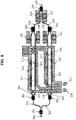
- Fig. 9 is a plan view of a conventional single-phase driving type IQ modulator disclosed in non-patent literature 4.
- the single-phase driving type IQ modulator is formed by an input waveguide 200, a 1 ⁇ 2 multimode interference (MMI) coupler 201 that demultiplexes light propagating through the input waveguide 200 into two systems, waveguides 202 and 203 that guide the two light components demultiplexed by the 1 ⁇ 2 MMI coupler 201, a 1 ⁇ 2 MMI coupler 204 that demultiplexes the light propagating through the waveguide 202 into two systems, a 1 ⁇ 2 MMI coupler 205 that demultiplexes the light propagating through the waveguide 203 into two systems, waveguides 206 and 207 that guide the two light components demultiplexed by the 1 ⁇ 2 MMI coupler 204, waveguides 208 and 209 that guide the two light components demultiplexed by the 1 ⁇ 2 MMI coupler 205, signal lines 210 to 213 configured to apply voltages to
- the signal line is as thick as about 100 ⁇ m.
- the electrical length difference of signals is generated between the two signal lines. Due to this electrical length difference, the frequency characteristic of the differential mode degrades, or a common mode and a mixed mode, which are causes of noise, are excited.
- a structure capable of bending signal lines of a differential configuration without exciting the common mode and without degrading the frequency characteristic of the differential mode is necessary.
- a modulator of a single-phase driving type to a driver to perform differential (SS) driving, as in non-patent literature 4.
- SS differential
- a common mode cannot propagate through a high-frequency line of the semiconductor MZ optical modulator.
- a common mode is totally reflected between the driver and the semiconductor MZ optical modulator, and this may undesirably cause crosstalk or the like and degrade the frequency characteristic or the driving force of the driver.
- the present invention has been made to solve the above-described problem, and has as its object to provide a semiconductor Mach-Zehnder optical modulator capable of solving degradation of the high-frequency characteristic of the modulator and having an excellent transmission characteristic by suppressing characteristic degradation caused by a phase difference in a differential mode at a bent portion and induction of a common mode that occurs due to the bent portion, which are problematic in a conventional structure, in a high-frequency wiring necessary for connecting to the terminal resistor of a signal line output terminal in a differential driving type semiconductor Mach-Zehnder optical modulator having a capacity loading structure, and an IQ modulator.
- a semiconductor Mach-Zehnder optical modulator comprising a first arm waveguide and a second arm waveguide, both formed on a substrate, and a first input-side lead line formed on a dielectric layer on the substrate and having one end to which a modulation signal is input, a second input-side lead line formed on the dielectric layer adjacent to the first input-side lead line and having one end to which a signal complementary to the modulation signal is input, a first phase modulation electrode line and a second phase modulation electrode line, both formed on the dielectric layer, and one-end sides of the first phase modulation electrode line and the second phase modulation electrode line being connected to other-end sides of the first input-side lead line and the second input-side lead line, respectively, a first output-side lead line and a second output-side lead line, both formed on the dielectric layer, and one-end sides of the first output-side lead line and the second output-side lead line being connected to other-end sides of the first phase modulation electrode line and
- the first and second phase modulation electrode lines are formed along the first and second arm waveguides, and the first and second output-side lead lines are bent in the direction crossing the extending direction of the first and second arm waveguides in the plane of the dielectric layer and connected to the terminal resistors. It is therefore possible to implement a semiconductor Mach-Zehnder optical modulator that can solve the degradation of the high-frequency characteristic as the problem in the conventional structure and have a broadband and is excellent in connection to a driver.
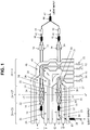
- Fig. 1 is a plan view showing the configuration of an IQ modulator according to the first embodiment of the present invention.
- the IQ modulator includes an input waveguide 10, a 1 ⁇ 2 MMI coupler 11 that demultiplexes light propagating through the input waveguide 10 into two systems, waveguides 12 and 13 that guide the two light components demultiplexed by the 1 ⁇ 2 MMI coupler 11, a 1 ⁇ 2 MMI coupler 14 that demultiplexes light propagating through the waveguide 12 into two systems, a 1 ⁇ 2 MMI coupler 15 that demultiplexes light propagating through the waveguide 13 into two systems, waveguides 16 and 17 (first and second arm waveguides) that guide the two light components demultiplexed by the 1 ⁇ 2 MMI coupler 14, waveguides 18 and 19 (first and second arm waveguides) that guide the two light components demultiplexed by the 1 ⁇ 2 MMI coupler 15, input-side lead lines 20 and 21 (first and second input-
- the IQ modulator further includes phase adjustment electrodes 36 to 39 made of a conductor and configured to adjust the phases of the modulated signal light components propagating through the waveguides 16 to 19, a 2 ⁇ 1 MMI coupler 40 that multiplexes the signal light components of two systems propagating through the waveguides 16 and 17, a 2 ⁇ 1 MMI coupler 41 that multiplexes the signal light components of two systems propagating through the waveguides 18 and 19, a waveguide 42 that guides the output light from the 2 ⁇ 1 MMI coupler 40, a waveguide 43 that guides the output light from the 2 ⁇ 1 MMI coupler 41, phase adjustment electrodes 44 and 45 made of a conductor and configured to adjust the phases of the signal light components propagating through the waveguides 42 and 43, a 2 ⁇ 1 MMI coupler 46 that multiplexes the signal light components of two systems propagating through the waveguides 42 and 43, an output waveguide 47, a ground line 48 made of a conductor and disposed in an outside of the input-side lead line 20, the phase modulation electrode line
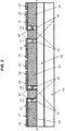
- Fig. 2 is a sectional view of the IQ modulator according to this embodiment taken along a line a - a'.
- reference numeral 60 denotes an n-InP layer; 61, a lower cladding layer made of InP; 62, a semiconductor core layer; 63, an upper cladding layer made of InP; 64, an SI-InP substrate; and 65, a dielectric layer formed on the n-InP layer 60.
- the input-side lead lines 20 to 23, the phase modulation electrode lines 24 to 27, the output-side lead lines 28 to 31, and the ground lines 48 to 50 are formed on the dielectric layer 65.
- a high-frequency line pattern according to this embodiment includes, as a basic structure, a GSSG (Ground Signal Ground) differential coplanar line, which comprises two signal lines and two ground lines, both formed on the dielectric layer 65 made of a low-k material.
- GSSG Gate Signal Ground
- a semiconductor MZ optical modulator using an I modulation signal as an input and a semiconductor MZ optical modulator using a Q modulation signal as an input are juxtaposed on the substrate, and the high-frequency line pattern of the semiconductor MZ optical modulator on the I modulation signal side and the high-frequency line pattern of the semiconductor MZ optical modulator on the Q modulation signal side share the ground line 49 at the center.
- the signal lines are formed by three portions, that is, the portion of the input-side lead lines 20 to 23, the portion of the phase modulation electrode lines 24 to 27, and the portion of the output-side lead lines 28 to 31, and all the portions form a differential line structure (GSSG configuration) with impedance matching. Since the differential line configuration is formed, the modulator can be driven by a differential input signal (differential driver) with a high energy efficiency.
- An I modulation signal is input from a differential driver (not shown) formed on the SI-InP substrate 64 to the input-side lead line 20, and an I modulation signal (bar I) complementary to that is input from the differential driver to the input-side lead line 21.
- a Q modulation signal is input from the differential driver to the input-side lead line 22, and a Q modulation signal (bar Q) complementary to that is input from the differential driver to the input-side lead line 23.
- each of the ground lines 48 to 50 is connected to the ground of the differential driver.
- the 1 ⁇ 2 MMI coupler 14, the waveguides 16 and 17, the input-side lead lines 20 and 21, the phase modulation electrode lines 24 and 25, the output-side lead lines 28 and 29, the electrodes 32 and 33, and the 2 ⁇ 1 MMI coupler 40 constitute the semiconductor MZ optical modulator on the I modulation signal side.
- the semiconductor MZ optical modulator modulates the phases of light components propagating through the waveguides 16 and 17 in accordance with the I modulation signals applied from the electrodes 32 and 33 to the waveguides 16 and 17.
- the 1 ⁇ 2 MMI coupler 15, the waveguides 18 and 19, the input-side lead lines 22 and 23, the phase modulation electrode lines 26 and 27, the output-side lead lines 30 and 31, the electrodes 34 and 35, and the 2 ⁇ 1 MMI coupler 41 constitute the semiconductor MZ optical modulator on the Q modulation signal side.
- the semiconductor MZ optical modulator modulates the phases of light components propagating through the waveguides 18 and 19 in accordance with the Q modulation signals applied from the electrodes 34 and 35 to the waveguides 18 and 19.
- the 2 ⁇ 1 MMI coupler 40 multiplexes the modulated signal light components propagating through the waveguides 16 and 17.
- the 2 ⁇ 1 MMI coupler 41 multiplexes the modulated signal light components propagating through the waveguides 18 and 19.
- phase adjustment can be performed such that the phase difference between the I-side signal light output from the 2 ⁇ 1 MMI coupler 40 and the Q-side signal light output from the 2 ⁇ 1 MMI coupler 41 becomes 90°.
- the 2 ⁇ 1 MMI coupler 46 multiplexes the I-side signal light propagating through the waveguide 42 and the Q-side signal light propagating through the waveguide 43, thereby obtaining an IQ-modulated optical signal.
- an IQ modulator can be implemented in this way.
- phase modulation electrode lines 24 to 27 are disposed in parallel to the waveguides 16 to 19 that constitute the semiconductor MZ optical modulators.
- the input-side lead lines 20 to 23 connected to the phase modulation electrode lines 24 to 27 need to be formed on the same lines as the phase modulation electrode lines 24 to 27.
- the structure preferably has no bending at all. This is because in the input-side lead lines 20 to 23, if bending occurs in the differential line structure, a common mode may occur due to the influence of a phase difference caused by the bent portion, and accordingly, the differential transmission characteristic may largely degrade, a resonance may occur, or a signal may be reflected by the bent portion and returned to the driver side to largely degrade the driving force of the driver.
- the line length increases as compared to a linear line, and this increases a propagation loss and also generates a bending loss. For this reason, the high-frequency characteristic of a differential signal degrades.
- the loss in the input-side lead lines 20 to 23 directly causes degradation of the modulation band.
- the lengths of the input-side lead lines 20 to 23 can be shortest.
- the input waveguide 10 and the 1 ⁇ 2 MMI coupler 11 are formed such that the light propagating direction (the vertical direction in Fig. 1 ) of the input waveguide 10 and the light input/output direction (the vertical direction in Fig. 1 ) of the 1 ⁇ 2 MMI coupler 11 become orthogonal to the extending direction (the horizontal direction in Fig. 1 ) of the waveguides 16 to 19, and the 1 ⁇ 2 MMI couplers 14, 15, 40, 41, and 46 are formed such that the input/output direction (the horizontal direction in Fig. 1 ) of the 1 ⁇ 2 MMI couplers 14, 15, 40, 41, and 46 becomes the same as the extending direction of the waveguides 16 to 19.
- the lengths of the input-side lead lines 20 to 23 can be set to 700 ⁇ m or less.
- the lengths can be made shorter by about 1 mm as compared to a conventional configuration described in a literature " N. Kono et al., "Compact and Low Power DP-QPSK Modulator Module with InP-Based Modulator and Driver ICs", OFC2013, OW1G.2, 2013 ".
- phase modulation electrode lines 24 to 27 will be described next.
- the phase modulation electrode lines 24 to 27 and the electrodes 32 to 35 connected to these have a differential capacity loading structure (GSSG configuration) that is excellent in impedance matching and speed matching between a microwave and an optical wave.
- GSSG configuration differential capacity loading structure
- the addition amounts of capacities to the phase modulation electrode lines 24 to 27 can freely be designed.
- the impedances of the phase modulation electrode lines 24 to 27 and the speeds of microwaves propagating through the phase modulation electrode lines 24 to 27 can be designed to arbitrary values.
- the electrodes 32 to 35 need to be designed such that these can be regarded as traveling wave electrodes.
- the periods of the electrodes 32 to 35 on a signal basis need to be set to at least 1/4 or less and, ideally, 1/8 or less of a guide wavelength ⁇ eff of modulation signals of the maximum frequency, which propagate through the phase modulation electrode lines 24 to 27 and the electrodes 32 to 35, such that the periods can be regarded as distribution constants.
- a Bragg frequency also needs to be considered in general.
- the Bragg frequency is a frequency on the high frequency side as compared to the frequency corresponding to the above-described guide wavelength, if the above-described condition to set the periods of the electrodes 32 to 35 on a signal basis to 1/4 or less (ideally, 1/8 or less) of the guide wavelength ⁇ eff is satisfied, the Bragg frequency need not be taken into consideration.
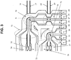
- Fig. 3 is an enlarged plan view of the portion of the output-side lead lines 28 to 31.
- the output-side lead lines 28 to 31 are bent in a direction crossing (in this embodiment, a direction orthogonal to) the extending direction of the waveguides 16 to 19 (the extending direction of the input-side lead lines 20 to 23 and the phase modulation electrode lines 24 to 27). Since the high-frequency line pattern according to this embodiment has a GSSG differential line structure, as described above, how to bend the output-side lead lines 28 to 31 is important.
- the width of the output-side lead lines 28 to 31 is set to a width for obtaining arbitrary impedances, and the output-side lead lines 28 to 31 having the width are bent at a right angle, electrical length differences are generated between the output-side lead lines 28 and 29 and between the output-side lead lines 30 and 31 of the differential configuration, and a large phase difference is generated. Due to the phase difference and asymmetry of bending, a common mode occurs, or the high-frequency characteristic of the differential mode degrades. This undesirably degrades the modulation band or degrades the transmission characteristic.
- the output-side lead lines 28 to 31 are formed in a predetermined width W1 corresponding to a desired impedance, and the width of the output-side lead lines 28 to 31 is gradually reduced in tapered portions (72 and 73 in Fig. 3 ) having a length of about 50 ⁇ m from positions closer to the phase modulation electrode lines 24 to 27 than bent portions (70 and 71 in Fig. 3 ) such that the width of the output-side lead lines 28 to 31 in the bent portions 70 and 71 becomes narrower than the predetermined width W1. Also, the distance between the output-side lead lines 28 and 29 and the distance between the output-side lead lines 30 and 31 are made shorter than the distance between the phase modulation electrode lines 24 and 25 and the distance between the phase modulation electrode lines 26 and 27.
- the distance between the output-side lead line 28 and the ground line 48, the distance between the output-side lead line 29 and the ground line 49, the distance between the output-side lead line 30 and the ground line 49, and the distance between the output-side lead line 31 and the ground line 50 are made shorter than the distances between the output-side lead lines and the ground lines in other portions.
- the widths of the ground lines 48 to 50 are equal in the bent portions and the linear portions, unlike the width of the output-side lead lines 28 to 31. This is because a satisfactory common mode characteristic is obtained, and a crosstalk characteristic is guaranteed.
- the line width is decreased only in a very small section much smaller than the wavelength (1/4 or less).
- the electrical length difference and the phase difference between the output-side lead lines 28 and 29 and the electrical length difference and the phase difference between the output-side lead lines 30 and 31 can be made sufficiently small. It is therefore possible to suppress occurrence of the common mode an degradation of the high-frequency characteristic of the differential mode.
- the transmission characteristic (Sdd21) can be improved by, for example, about 0.5 dB at 50 GHz, as compared to the conventional configuration in which the output-side lead lines are wired in a predetermined width.
- Sdc21 representing conversion from the differential mode to the common mode (induction of the common mode) can be improved by, for example, about 10 dB.
- a width W2 of the ground lines 48 to 50 is preferably constant to minimize the asymmetry of the structure.
- the high-frequency characteristic can further be improved.
- the differential reflection characteristic (Sdd11) can be improved by several dB, as compared to a normal curve.
- the width of the output-side lead lines 28 to 31 in the bent portions 70 and 71 is made narrower than the predetermined width W1 of linear portions where impedance matching is obtained, as described above.
- the bent portions 70 and 71 may serve as signal reflecting points due to the influence of slight impedance mismatching caused by making the width of the output-side lead lines 28 to 31 narrower, and the high-frequency characteristic may degrade.
- the propagation lengths in the bent portions 70 and 71 are preferably set to 1/4 or less and, if possible, 1/8 or less of the guide wavelength ⁇ eff .
- the propagation lengths in the tapered portions 72 and 73 are preferably 50 ⁇ m or less.
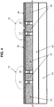
- the output-side lead lines 28 to 31 are basically formed on the dielectric layer 65. However, when the output-side lead lines 28 to 31 are bent, portions where the output-side lead lines 28 to 31 are formed on the waveguides 16 to 19 are generated, as shown in Fig. 4 showing a section taken along a line b - b' in Fig. 3 . That is, the output-side lead lines 28 to 31 cross over a semiconductor whose dielectric constant is about four times larger than that of benzocyclobutene that is an example of the low-k material forming the dielectric layer 65.
- the impedances of the output-side lead lines 28 to 31 may largely lower, and impedance mismatching may occur.
- the width of the output-side lead lines 28 to 31 may be made smaller than the predetermined width W1 corresponding to a desired impedance, as in the bent portions 70 and 71, and the distance between the output-side lead lines 28 and 29, the distance between the output-side lead line 28 and the ground line 48, and the distance between the output-side lead line 29 and the ground line 49 may be decreased.
- the structures of the output-side lead lines 28 to 31 and the ground lines 48 and 49 in the crossing portions as described above are not essential components of the present invention. If the area where the output-side lead lines 28 to 31 cross over the waveguides 16 to 19 is small, the influence of impedance mismatching is not observed. Hence, the structures are unnecessary.
- the distance between the output-side lead lines 28 and 29 and the distance between the output-side lead lines 30 and 31 are shortened as compared to the portions of the phase modulation electrode lines 24 to 27. This makes it possible to obtain a structure capable of increasing electrical confinement and prevent electromagnetic wave leakage in the substrate direction or substrate resonance.
- the end portions of the output-side lead lines 28 to 31 are connected to the terminal resistors 51 to 54 that satisfy desired differential impedances and common mode impedances and are differentially terminated.
- wires 55 and 56 that electrically connect the ground lines 48 to 50 are preferably provided in actuality.
- the wires 55 connect the ground lines 48 and 49.
- the wires 56 connect the ground lines 49 and 50. If the wires 55 and 56 are absent, the potentials of the ground lines 48 to 50 are not stable and fluctuate. Hence, resonance occurs at an arbitrary frequency depending on the propagation length. It is therefore difficult to implement a broadband modulator.
- the wires 55 and 56 that connect the ground lines 48 to 50 are preferably provided at a period much shorter than the signal wavelength along the signal propagation direction, that is, at a period 1/4 to 1/8 or less of the guide wavelength ⁇ eff .
- the wires 55 and 56 are provided only in the portions of the output-side lead lines 28 to 31. However, in the portions of the input-side lead lines 20 to 23 and the phase modulation electrode lines 24 to 27 as well, the wires 55 and 56 are preferably similarly provided between the ground lines 48 to 50.
- a broadband modulator in which the potentials of the ground lines 48 to 50 on both sides of the input-side lead lines 20 to 23, the phase modulation electrode lines 24 to 27, and the output-side lead lines 28 to 31, and the resonance of the potentials of the ground lines 48 to 50 can be suppressed can be implemented. If the wires 55 and 56 are provided at a period longer than 1/4 to 1/8 of the guide wavelength ⁇ eff , the amount of ripple can be reduced. However, it is impossible to completely suppress the resonance of the potentials of the ground lines 48 to 50.
- the potentials of the ground lines 48 to 50 may be stabilized by connecting the ground lines 48 to 50 via a ground electrode 80 provided on the lower surface of the semiconductor substrate (SI-InP substrate 64) and ground vias 81 to 84 formed by processing the semiconductor substrate.
- the ground vias 81 connect the ground line 48 and the ground electrode 80.
- the ground vias 82 and 83 connect the ground line 49 and the ground electrode 80.
- the ground vias 84 connect the ground line 50 and the ground electrode 80.
- lines 85 that connect the pairs of ground vias 81 and 82 periodically provided on the ground lines 48 and 49 at a period of 1/4 to 1/8 or less of the guide wavelength ⁇ eff are illustrated.
- lines 86 that connect the pairs of ground vias 83 and 84 periodically provided on the ground lines 49 and 50 at a period of 1/4 to 1/8 or less of the guide wavelength ⁇ eff are illustrated.
- the ground vias 81 to 84 are provided only in the portions of the output-side lead lines 28 to 31, as in Fig. 5 . However, in the portions of the input-side lead lines 20 to 23 and the phase modulation electrode lines 24 to 27 as well, the ground vias 81 to 84 are preferably provided between the ground lines 48 to 50.
- the ground electrode 80 is formed on the lower surface of the semiconductor substrate.
- a dielectric layer may be formed on the structure shown in Figs. 1 to 4 , and the ground electrode 80 may be formed on the dielectric layer.
- Fig. 7 is a plan view showing the configuration of an IQ modulator according to the second embodiment of the present invention, and the same reference numerals as in Fig. 1 denote the same components.
- the light propagation direction of the input waveguide 10 is orthogonal to the extending direction (the horizontal direction in Fig. 1 ) of the waveguides 16 to 19.
- the lengths of input-side lead lines 20 to 23 can be set to 700 ⁇ m or less.
- the lengths can be made shorter by about 1 mm as compared to a conventional configuration described in a literature " N. Kono et al., "Compact and Low Power DP-QPSK Modulator Module with InP-Based Modulator and Driver ICs", OFC2013, OW1G.2, 2013 ".
- the waveguides 16 to 19 of the semiconductor MZ optical modulator each have a structure formed by sequentially stacking the lower cladding layer 61 made of InP, the non-doped semiconductor core layer 62, and the upper cladding layer 63 made of InP on the SI-InP substrate 64. This also applies to the remaining waveguides 10, 10a, 12, 13, 42, 43, and 47.
- the semiconductor core layer 62 functions as an optical waveguide layer and is made of a material such as, for example, InGaAsP or InGaAlAs.
- the semiconductor core layer 62 is preferably formed by a bulk layer of a quaternary mixed crystal with a single composition or a multiple quantum well layer.
- a structure obtained by forming, on the upper and lower sides of the multiple quantum well layer, light confinement layers whose bandgap is larger than that of the multiple quantum well layer and smaller than that of the lower cladding layer 61 and the upper cladding layer 63 may be used as the semiconductor core layer 62.
- the bandgap wavelength of the bulk layer of a quaternary mixed crystal or the multiple quantum well layer is set such that the electrooptic effect effectively acts at the optical wavelength to be used, and light absorption is not problematic.
- the dielectric layer 65 can reduce the electrode loss, and is therefore preferably made of a low-k material such as, for example, polyimide or BCB, which is an organic material.
- a low-k material such as, for example, polyimide or BCB, which is an organic material.
- the present invention is not limited to an InP-based material, and, for example, a material system matching a GaAs substrate may be used.
- One of the upper cladding layer 63 and the lower cladding layer 61 may be made of an n-type semiconductor, and the other may be made of a p-type semiconductor. It is also possibly to employ a structure in which both the semiconductor core layer 62 and the lower cladding layer 61 are made of an n-type semiconductor, and a third p-type cladding layer is inserted between the upper cladding layer 63 and the semiconductor core layer 62 or between the lower cladding layer 61 and the semiconductor core layer 62.
- the present invention can be applied to a semiconductor Mach-Zehnder optical modulator that modulates an optical signal by an electrical signal.
Landscapes
- Physics & Mathematics (AREA)
- Nonlinear Science (AREA)
- General Physics & Mathematics (AREA)
- Optics & Photonics (AREA)
- Electromagnetism (AREA)
- Optical Modulation, Optical Deflection, Nonlinear Optics, Optical Demodulation, Optical Logic Elements (AREA)
Abstract
Description
- The present invention relates to a semiconductor Mach-Zehnder optical modulator that modulates an optical signal by an electrical signal, and an IQ modulator using the semiconductor Mach-Zehnder optical modulator.
- To cope with an increasing communication traffic demand, a high-speed optical modulator compatible with an advanced optical modulation method has been required. In particular, multilevel optical modulators using a digital coherent technique have played a major role in implementing a transceiver with a large capacity more than 100 Gbps. In the multilevel optical modulators, to add independent signals to the amplitude and the phase of light, Mach-Zehnder (MZ) interference type optical modulators capable of zero chirp driving are parallelly incorporated in multiple stages.
- In recent years, how to reduce the size of an optical transmitter module and how to implement a low driving voltage have become problems, and R&D on a compact semiconductor MZ optical modulator capable of lowering the driving voltage has been vigorously conducted (see non-patent
literatures 1 and 2).Figs. 8A and8B show an example of a conventional semiconductor MZ optical modulator.Fig. 8A is a plan view of a semiconductor MZ optical modulator, andFig. 8B is a sectional view taken along a line c - c' inFig. 8A . - Referring to
Figs. 8A and8B ,reference numeral 101 denotes an input waveguide of a semiconductor MZ optical modulator; 102, an output waveguide; 103, an optical demultiplexer that demultiplexes an optical wave propagating through theinput waveguide 101 into twowaveguides waveguides output waveguide 102; 109 and 110, coplanar strip lines; and 111 and 112, electrodes configured to apply voltages to thewaveguides - Referring to
Fig. 8B ,reference numeral 113 denotes an n-InP layer; 114, a lower cladding layer made of InP; 115, a semiconductor core layer through which an optical wave propagates; 116, an upper cladding layer made of InP; and 117, an SI-InP substrate. - The
input waveguide 101, theoutput waveguide 102, theoptical demultiplexer 103, thewaveguides optical multiplexer 106 form an MZ interferometer. In the MZ interferometer, when voltages are applied to thewaveguides semiconductor core layer 115 due to an electrooptic effect, and as a result, the phase of light changes. At this time, when a voltage difference is set between thewaveguides optical multiplexer 106 changes, and the light can be modulated (that is, output light from theoutput waveguide 102 is turned on or off). - An SG configuration is formed in which if one of the two
coplanar strip lines - A microwave propagating through the
coplanar strip lines waveguides electrodes electrodes coplanar strip lines waveguides - In fact, since a microwave loss, microwave reflection derived from impedance mismatching, and a phase shift between the optical wave and the microwave occur, the modulation band is limited due to these reasons.
- Since the
upper cladding layer 116, thesemiconductor core layer 115, and thelower cladding layer 114 exist under theelectrodes Fig. 8A , theelectrodes coplanar strip lines - That is, when the number and interval of the
electrodes electrodes waveguides coplanar strip lines coplanar strip lines coplanar strip lines - As described above, in the semiconductor MZ optical modulator with a capacity loading structure, when optimum capacity addition amounts to the
coplanar strip lines - The semiconductor MZ optical modulator with the configuration shown in
Figs. 8A and8B is of single-phase driving type. However, when connection to a driver of differential driving type or power consumption is taken into consideration, the optical modulator side is also preferably formed as a differential driving type (for example, GSSG configuration) (see non-patent literature 3). - Also, the optical modulator of differential driving type is excellent in suppressing crosstalk, unlike the single-phase driving type, and is therefore advantageous in implementing a polarization multiplex IQ modulator integrated on one chip. Considering the layout of the modulator chip, to connect a signal line to a driver and a terminal resistor, the signal line needs to be bent somewhere such that the signal line reaches a chip end. However, in a case in which an optical modulator is of differential driving type, like an IQ modulator of single-phase driving type disclosed in non-patent literature 4, if a signal line of a differential configuration is bent almost at a right angle, a large phase difference is generated between two signal lines that form a differential pair, and the differential characteristic degrades, or a common mode that is a noise component is induced, and the transmission characteristic of the modulator degrades.
-
Fig. 9 is a plan view of a conventional single-phase driving type IQ modulator disclosed in non-patent literature 4. The single-phase driving type IQ modulator is formed by aninput waveguide 200, a 1×2 multimode interference (MMI)coupler 201 that demultiplexes light propagating through theinput waveguide 200 into two systems,waveguides MMI coupler 201, a 1×2MMI coupler 204 that demultiplexes the light propagating through thewaveguide 202 into two systems, a 1×2MMI coupler 205 that demultiplexes the light propagating through thewaveguide 203 into two systems,waveguides MMI coupler 204,waveguides MMI coupler 205,signal lines 210 to 213 configured to apply voltages to thewaveguides 206 to 209,electrodes 214 to 217 that apply the voltages supplied from thesignal lines 210 to 213 to thewaveguides 206 to 209,phase adjustment electrodes 218 to 221 configured to adjust the phases of modulated signal light components propagating through thewaveguides 206 to 209, a 2×1MMI coupler 222 that multiplexes the signal light components of two systems propagating through thewaveguides MMI coupler 223 that multiplexes the signal light components of two systems propagating through thewaveguides waveguide 224 that guides output light from the 2×1MMI coupler 222, awaveguide 225 that guides output light from the 2×1MMI coupler 223,phase adjustment electrodes waveguides MMI coupler 228 that multiplexes the signal light components of two systems propagating through thewaveguides output waveguide 229. One-end sides of thesignal lines 210 to 213 are connected todrivers signal lines 210 to 213 are connected to terminal resistors (not shown). - The reason why it is difficult to bend the signal line in differential driving is as follows. In the semiconductor MZ optical modulator with the capacity loading structure, the signal line is as thick as about 100 µm. Hence, when two signal lines of a differential configuration are bent, the electrical length difference of signals is generated between the two signal lines. Due to this electrical length difference, the frequency characteristic of the differential mode degrades, or a common mode and a mixed mode, which are causes of noise, are excited. Hence, a structure capable of bending signal lines of a differential configuration without exciting the common mode and without degrading the frequency characteristic of the differential mode is necessary.
- It is also possible to connect a modulator of a single-phase driving type to a driver to perform differential (SS) driving, as in non-patent literature 4. In this case, however, a common mode cannot propagate through a high-frequency line of the semiconductor MZ optical modulator. There is a concern that a common mode is totally reflected between the driver and the semiconductor MZ optical modulator, and this may undesirably cause crosstalk or the like and degrade the frequency characteristic or the driving force of the driver.
-
- Non-Patent Literature 1: L. Morl et al., "A travelling wave electrode Mach-Zehnder 40 Gb/s demultiplexer based on strain compensated GaInAs/AlInAs tunnelling barrier MQW structure", 1998 International Conference on Indium Phosphide and Related Materials, pp. 403-406, 1998
- Non-Patent Literature 2: H. N. Klein et al., "1.55 µm Mach-Zehnder Modulators on InP for optical 40/80 Gbit/s transmission networks", OFC2006, pp. 171-173, 2006
- Non-Patent Literature 3: K. Prosyk et al., "Travelling Wave Mach-Zehnder Modulators", IPRM2013, MoD 3-1, 2013
- Non-Patent Literature 4: S. Lange et al., "Low Power InP-Based Monolithic DFB-Laser IQ Modulator With SiGe Differential Driver for 32-GBd QPSK Modulation", JOURNAL OF LIGHTWAVE TECHNOLOGY, VOL. 34, NO.8, APRIL 15,2016
- The present invention has been made to solve the above-described problem, and has as its object to provide a semiconductor Mach-Zehnder optical modulator capable of solving degradation of the high-frequency characteristic of the modulator and having an excellent transmission characteristic by suppressing characteristic degradation caused by a phase difference in a differential mode at a bent portion and induction of a common mode that occurs due to the bent portion, which are problematic in a conventional structure, in a high-frequency wiring necessary for connecting to the terminal resistor of a signal line output terminal in a differential driving type semiconductor Mach-Zehnder optical modulator having a capacity loading structure, and an IQ modulator.
- According to the present invention, there is provided a semiconductor Mach-Zehnder optical modulator comprising a first arm waveguide and a second arm waveguide, both formed on a substrate, and a first input-side lead line formed on a dielectric layer on the substrate and having one end to which a modulation signal is input, a second input-side lead line formed on the dielectric layer adjacent to the first input-side lead line and having one end to which a signal complementary to the modulation signal is input, a first phase modulation electrode line and a second phase modulation electrode line, both formed on the dielectric layer, and one-end sides of the first phase modulation electrode line and the second phase modulation electrode line being connected to other-end sides of the first input-side lead line and the second input-side lead line, respectively, a first output-side lead line and a second output-side lead line, both formed on the dielectric layer, and one-end sides of the first output-side lead line and the second output-side lead line being connected to other-end sides of the first phase modulation electrode line and the second phase modulation electrode line, respectively, a first electrode and a second electrode, which are configured to apply the modulation signals propagating through the first phase modulation electrode line and the second phase modulation electrode line to the first arm waveguide and the second arm waveguide, respectively, a first ground line formed on the dielectric layer along a propagation direction of the modulation signal and in an outside of the first input-side lead line, the first phase modulation electrode line and the first output-side lead line, a second ground line formed on the dielectric layer along the propagation direction of the modulation signal and in an outside of the second input-side lead line, the second phase modulation electrode line and the second output-side lead line, and terminal resistors connected to other-end sides of the first output-side lead line and the second output-side lead line, wherein the first phase modulation electrode line and the second phase modulation electrode line are formed along the first arm waveguide and the second arm waveguide and the first output-side lead line and the second output-side lead line are bent in a direction crossing an extending direction of the first arm waveguide and the second arm waveguide in a plane of the dielectric layer and connected to the terminal resistors.
- According to the present invention, the first and second phase modulation electrode lines are formed along the first and second arm waveguides, and the first and second output-side lead lines are bent in the direction crossing the extending direction of the first and second arm waveguides in the plane of the dielectric layer and connected to the terminal resistors. It is therefore possible to implement a semiconductor Mach-Zehnder optical modulator that can solve the degradation of the high-frequency characteristic as the problem in the conventional structure and have a broadband and is excellent in connection to a driver.
-
-
Fig. 1 is a plan view showing the configuration of an IQ modulator according to the first embodiment of the present invention; -
Fig. 2 is a sectional view of the IQ modulator according to the first embodiment of the present invention; -
Fig. 3 is an enlarged plan view of the portion of the output-side lead lines of the IQ modulator according to the first embodiment of the present invention; -
Fig. 4 is a sectional view of the bent portions of the output-side lead lines of the IQ modulator according to the first embodiment of the present invention; -
Fig. 5 is a plan view showing wires that connect ground lines in the first embodiment of the present invention; -
Fig. 6 is a plan view showing ground vias that connect the ground lines in the first embodiment of the present invention; -
Fig. 7 is a plan view showing the configuration of an IQ modulator according to the second embodiment of the present invention; -
Fig. 8A is a plan view showing the configuration of a conventional semiconductor Mach-Zehnder optical modulator; -
Fig. 8B is a sectional view showing the configuration of the conventional semiconductor Mach-Zehnder optical modulator; and -
Fig. 9 is a plan view showing the configuration of a conventional single-phase driving type IQ modulator. - An embodiment of the present invention will now be described with reference to the accompanying drawings.
Fig. 1 is a plan view showing the configuration of an IQ modulator according to the first embodiment of the present invention. The IQ modulator includes an input waveguide 10, a 1×2 MMI coupler 11 that demultiplexes light propagating through the input waveguide 10 into two systems, waveguides 12 and 13 that guide the two light components demultiplexed by the 1×2 MMI coupler 11, a 1×2 MMI coupler 14 that demultiplexes light propagating through the waveguide 12 into two systems, a 1×2 MMI coupler 15 that demultiplexes light propagating through the waveguide 13 into two systems, waveguides 16 and 17 (first and second arm waveguides) that guide the two light components demultiplexed by the 1×2 MMI coupler 14, waveguides 18 and 19 (first and second arm waveguides) that guide the two light components demultiplexed by the 1×2 MMI coupler 15, input-side lead lines 20 and 21 (first and second input-side lead lines) made of a conductor and configured to apply I modulation signals to the waveguides 16 and 17, input-side lead lines 22 and 23 (first and second input-side lead lines) made of a conductor and configured to apply Q modulation signals to the waveguides 18 and 19, phase modulation electrode lines 24 and 25 (first and second phase modulation electrode lines) made of a conductor and connected to the input-side lead lines 20 and 21, phase modulation electrode lines 26 and 27 (first and second phase modulation electrode lines) made of a conductor and connected to the input-side lead lines 22 and 23, output-side lead lines 28 and 29 (first and second output-side lead lines) made of a conductor and connected to the phase modulation electrode lines 24 and 25, output-side lead lines 30 and 31 (first and second output-side lead lines) made of a conductor and connected to the phase modulation electrode lines 26 and 27, electrodes 32 and 33 (first and second electrodes) made of a conductor and configured to apply the I modulation signals supplied from the phase modulation electrode lines 24 and 25 to the waveguides 16 and 17, and electrodes 34 and 35 (first and second electrodes) made of a conductor and configured to apply the Q modulation signals supplied from the phase modulation electrode lines 26 and 27 to the waveguides 18 and 19. - The IQ modulator further includes phase adjustment electrodes 36 to 39 made of a conductor and configured to adjust the phases of the modulated signal light components propagating through the waveguides 16 to 19, a 2×1 MMI coupler 40 that multiplexes the signal light components of two systems propagating through the waveguides 16 and 17, a 2×1 MMI coupler 41 that multiplexes the signal light components of two systems propagating through the waveguides 18 and 19, a waveguide 42 that guides the output light from the 2×1 MMI coupler 40, a waveguide 43 that guides the output light from the 2×1 MMI coupler 41, phase adjustment electrodes 44 and 45 made of a conductor and configured to adjust the phases of the signal light components propagating through the waveguides 42 and 43, a 2×1 MMI coupler 46 that multiplexes the signal light components of two systems propagating through the waveguides 42 and 43, an output waveguide 47, a ground line 48 made of a conductor and disposed in an outside of the input-side lead line 20, the phase modulation electrode line 24, and the output-side lead line 28, a ground line 49 made of a conductor and disposed between the input-side lead line 21, the phase modulation electrode line 25, and the output-side lead line 29 and the input-side lead line 22, the phase modulation electrode line 26, and the output-side lead line 30, a ground line 50 made of a conductor and disposed in an outside of the input-side lead line 23, the phase modulation electrode line 27, and the output-side lead line 31, and terminal resistors 51 to 54 connected to the end portions of the output-side lead lines 28 to 31.
-
Fig. 2 is a sectional view of the IQ modulator according to this embodiment taken along a line a - a'. Referring toFig. 2 ,reference numeral 60 denotes an n-InP layer; 61, a lower cladding layer made of InP; 62, a semiconductor core layer; 63, an upper cladding layer made of InP; 64, an SI-InP substrate; and 65, a dielectric layer formed on the n-InP layer 60. - As shown in
Fig. 2 , the input-side lead lines 20 to 23, the phasemodulation electrode lines 24 to 27, the output-side lead lines 28 to 31, and the ground lines 48 to 50 are formed on thedielectric layer 65. - These high-frequency line patterns will be described next in more detail. A high-frequency line pattern according to this embodiment includes, as a basic structure, a GSSG (Ground Signal Ground) differential coplanar line, which comprises two signal lines and two ground lines, both formed on the
dielectric layer 65 made of a low-k material. - In this embodiment, a semiconductor MZ optical modulator using an I modulation signal as an input and a semiconductor MZ optical modulator using a Q modulation signal as an input are juxtaposed on the substrate, and the high-frequency line pattern of the semiconductor MZ optical modulator on the I modulation signal side and the high-frequency line pattern of the semiconductor MZ optical modulator on the Q modulation signal side share the
ground line 49 at the center. - The signal lines are formed by three portions, that is, the portion of the input-side lead lines 20 to 23, the portion of the phase
modulation electrode lines 24 to 27, and the portion of the output-side lead lines 28 to 31, and all the portions form a differential line structure (GSSG configuration) with impedance matching. Since the differential line configuration is formed, the modulator can be driven by a differential input signal (differential driver) with a high energy efficiency. - An I modulation signal is input from a differential driver (not shown) formed on the SI-
InP substrate 64 to the input-side lead line 20, and an I modulation signal (bar I) complementary to that is input from the differential driver to the input-side lead line 21. Similarly, a Q modulation signal is input from the differential driver to the input-side lead line 22, and a Q modulation signal (bar Q) complementary to that is input from the differential driver to the input-side lead line 23. - End portions of the output-side lead lines 28 to 31 are terminated by the
terminal resistors 51 to 54. - One end (the left end portion in
Fig. 1 ) of each of the ground lines 48 to 50 is connected to the ground of the differential driver. - The 1×2
MMI coupler 14, thewaveguides modulation electrode lines electrodes MMI coupler 40 constitute the semiconductor MZ optical modulator on the I modulation signal side. The semiconductor MZ optical modulator modulates the phases of light components propagating through thewaveguides electrodes waveguides - Similarly, the 1×2
MMI coupler 15, thewaveguides modulation electrode lines electrodes MMI coupler 41 constitute the semiconductor MZ optical modulator on the Q modulation signal side. The semiconductor MZ optical modulator modulates the phases of light components propagating through thewaveguides electrodes waveguides - The 2×1
MMI coupler 40 multiplexes the modulated signal light components propagating through thewaveguides MMI coupler 41 multiplexes the modulated signal light components propagating through thewaveguides phase adjustment electrodes MMI coupler 40 and the Q-side signal light output from the 2×1MMI coupler 41 becomes 90°. - The 2×1
MMI coupler 46 multiplexes the I-side signal light propagating through thewaveguide 42 and the Q-side signal light propagating through thewaveguide 43, thereby obtaining an IQ-modulated optical signal. In this embodiment, an IQ modulator can be implemented in this way. - Characteristic configurations of this embodiment will sequentially be described next. The phase
modulation electrode lines 24 to 27 are disposed in parallel to thewaveguides 16 to 19 that constitute the semiconductor MZ optical modulators. - The input-side lead lines 20 to 23 connected to the phase
modulation electrode lines 24 to 27 need to be formed on the same lines as the phasemodulation electrode lines 24 to 27. In addition, the structure preferably has no bending at all. This is because in the input-side lead lines 20 to 23, if bending occurs in the differential line structure, a common mode may occur due to the influence of a phase difference caused by the bent portion, and accordingly, the differential transmission characteristic may largely degrade, a resonance may occur, or a signal may be reflected by the bent portion and returned to the driver side to largely degrade the driving force of the driver. - Also, if bending occurs in the input-side lead lines 20 to 23, the line length increases as compared to a linear line, and this increases a propagation loss and also generates a bending loss. For this reason, the high-frequency characteristic of a differential signal degrades. In particular, the loss in the input-side lead lines 20 to 23 directly causes degradation of the modulation band. Hence, to implement a boarder band, it is important to minimize the loss in the input-side lead lines 20 to 23.
- To minimize the loss in the input-side lead lines 20 to 23, it is necessary not only to form the input-side lead lines 20 to 23 on the same lines as the phase
modulation electrode lines 24 to 27, as described above, but also to optimize the arrangement of thewaveguides 16 to 19, the input-side lead lines 20 to 23, and the phasemodulation electrode lines 24 to 27. - For example, with the arrangement as in this embodiment, the lengths of the input-side lead lines 20 to 23 can be shortest. In this embodiment, the
input waveguide 10 and the 1×2MMI coupler 11 are formed such that the light propagating direction (the vertical direction inFig. 1 ) of theinput waveguide 10 and the light input/output direction (the vertical direction inFig. 1 ) of the 1×2MMI coupler 11 become orthogonal to the extending direction (the horizontal direction inFig. 1 ) of thewaveguides 16 to 19, and the 1×2MMI couplers Fig. 1 ) of the 1×2MMI couplers waveguides 16 to 19. This forms the waveguide patterns in an L-shaped layout. - According to this layout, the lengths of the input-side lead lines 20 to 23 can be set to 700 µm or less. The lengths can be made shorter by about 1 mm as compared to a conventional configuration described in a literature "N. Kono et al., "Compact and Low Power DP-QPSK Modulator Module with InP-Based Modulator and Driver ICs", OFC2013, OW1G.2, 2013".
- The phase
modulation electrode lines 24 to 27 will be described next. The phasemodulation electrode lines 24 to 27 and theelectrodes 32 to 35 connected to these have a differential capacity loading structure (GSSG configuration) that is excellent in impedance matching and speed matching between a microwave and an optical wave. That is, theground line 48, the phasemodulation electrode line 24 to which the I modulation signal is input, theelectrode 32 to which the I modulation signal is supplied from the phasemodulation electrode line 24, theelectrode 33 to which the signal (bar I) complementary to the I modulation signal is input, the phasemodulation electrode line 25 that supplies the signal to theelectrode 33, theground line 49, the phasemodulation electrode line 26 to which the Q modulation signal is input, theelectrode 34 to which the Q modulation signal is supplied from the phasemodulation electrode line 26, theelectrodes 32 to 35 to which the signal (bar Q) complementary to the Q modulation signal is input, the phasemodulation electrode line 27 that supplies the signal to theelectrode 35, and theground line 50 are juxtaposed. - When the number, the interval, and the length of the
electrodes 32 to 35 in the capacity loading portion, which are branched from the phasemodulation electrode lines 24 to 27 serving as main lines and periodically formed, are optimally designed, the addition amounts of capacities to the phasemodulation electrode lines 24 to 27 can freely be designed. Hence, the impedances of the phasemodulation electrode lines 24 to 27 and the speeds of microwaves propagating through the phasemodulation electrode lines 24 to 27 can be designed to arbitrary values. - It is therefore possible to form an electrode configuration capable of simultaneously implementing impedance matching and speed matching between a microwave and an optical wave and implementing a broadband operation of the modulator at 30 GHz or more. In addition, to cause the semiconductor MZ optical modulator to perform the broadband operation, the
electrodes 32 to 35 need to be designed such that these can be regarded as traveling wave electrodes. For this reason, the periods of theelectrodes 32 to 35 on a signal basis need to be set to at least 1/4 or less and, ideally, 1/8 or less of a guide wavelength λeff of modulation signals of the maximum frequency, which propagate through the phasemodulation electrode lines 24 to 27 and theelectrodes 32 to 35, such that the periods can be regarded as distribution constants. - To periodically arrange the
electrodes 32 to 35 along the extending direction of thewaveguides 16 to 19, a Bragg frequency also needs to be considered in general. In this embodiment, however, since the Bragg frequency is a frequency on the high frequency side as compared to the frequency corresponding to the above-described guide wavelength, if the above-described condition to set the periods of theelectrodes 32 to 35 on a signal basis to 1/4 or less (ideally, 1/8 or less) of the guide wavelength λeff is satisfied, the Bragg frequency need not be taken into consideration. - The output-side lead lines 28 to 31 will be described next.
Fig. 3 is an enlarged plan view of the portion of the output-side lead lines 28 to 31. As for the structure, in the plane of the dielectric layer 65 (in the sheet surface ofFig. 3 ), the output-side lead lines 28 to 31 are bent in a direction crossing (in this embodiment, a direction orthogonal to) the extending direction of thewaveguides 16 to 19 (the extending direction of the input-side lead lines 20 to 23 and the phasemodulation electrode lines 24 to 27). Since the high-frequency line pattern according to this embodiment has a GSSG differential line structure, as described above, how to bend the output-side lead lines 28 to 31 is important. - For example, if the width of the output-side lead lines 28 to 31 is set to a width for obtaining arbitrary impedances, and the output-side lead lines 28 to 31 having the width are bent at a right angle, electrical length differences are generated between the output-side lead lines 28 and 29 and between the output-side lead lines 30 and 31 of the differential configuration, and a large phase difference is generated. Due to the phase difference and asymmetry of bending, a common mode occurs, or the high-frequency characteristic of the differential mode degrades. This undesirably degrades the modulation band or degrades the transmission characteristic.
- In this embodiment, the output-side lead lines 28 to 31 are formed in a predetermined width W1 corresponding to a desired impedance, and the width of the output-side lead lines 28 to 31 is gradually reduced in tapered portions (72 and 73 in
Fig. 3 ) having a length of about 50 µm from positions closer to the phasemodulation electrode lines 24 to 27 than bent portions (70 and 71 inFig. 3 ) such that the width of the output-side lead lines 28 to 31 in thebent portions modulation electrode lines modulation electrode lines bent portions side lead line 28 and theground line 48, the distance between the output-side lead line 29 and theground line 49, the distance between the output-side lead line 30 and theground line 49, and the distance between the output-side lead line 31 and theground line 50 are made shorter than the distances between the output-side lead lines and the ground lines in other portions. However, at this time, the widths of the ground lines 48 to 50 are equal in the bent portions and the linear portions, unlike the width of the output-side lead lines 28 to 31. This is because a satisfactory common mode characteristic is obtained, and a crosstalk characteristic is guaranteed. - In this embodiment, the line width is decreased only in a very small section much smaller than the wavelength (1/4 or less). Hence, in both the differential mode and the common mode, even if the impedances of the output-side lead lines 28 to 31 are made high, the output-side lead lines 28 to 31 can be bent without any characteristic degradation caused by impedance mismatching.
- When the width of the output-side lead lines 28 to 31 is reduced in the
bent portions - In this embodiment, the transmission characteristic (Sdd21) can be improved by, for example, about 0.5 dB at 50 GHz, as compared to the conventional configuration in which the output-side lead lines are wired in a predetermined width. Also, Sdc21 representing conversion from the differential mode to the common mode (induction of the common mode) can be improved by, for example, about 10 dB.
- In addition, to prevent characteristic degradation of the common mode, a width W2 of the ground lines 48 to 50 is preferably constant to minimize the asymmetry of the structure.
- Also, when clothoid curves are employed as the tracks of the edges of the output-side lead lines 28 to 31 in the
bent portions - In this embodiment, the width of the output-side lead lines 28 to 31 in the
bent portions bent portions bent portions bent portions portions - Additionally, the output-side lead lines 28 to 31 are basically formed on the
dielectric layer 65. However, when the output-side lead lines 28 to 31 are bent, portions where the output-side lead lines 28 to 31 are formed on thewaveguides 16 to 19 are generated, as shown inFig. 4 showing a section taken along a line b - b' inFig. 3 . That is, the output-side lead lines 28 to 31 cross over a semiconductor whose dielectric constant is about four times larger than that of benzocyclobutene that is an example of the low-k material forming thedielectric layer 65. For this reason, if the output-side lead lines 28 to 31 are formed on thewaveguides 16 to 19 while maintaining the width on thedielectric layer 65, the impedances of the output-side lead lines 28 to 31 may largely lower, and impedance mismatching may occur. - Even in a cross portion (74 in
Figs. 3 and4 ) other than thebent portions bent portions side lead line 28 and theground line 48, and the distance between the output-side lead line 29 and theground line 49 may be decreased. - With this structure, in the portions where the output-side lead lines 28 to 31 cross over the
waveguides 16 to 19, the possibility that the impedances of the output-side lead lines 28 to 31 largely lower, and impedance mismatching occurs can be reduced. However, the structures of the output-side lead lines 28 to 31 and the ground lines 48 and 49 in the crossing portions as described above are not essential components of the present invention. If the area where the output-side lead lines 28 to 31 cross over thewaveguides 16 to 19 is small, the influence of impedance mismatching is not observed. Hence, the structures are unnecessary. - Also, in this embodiment, the distance between the output-side lead lines 28 and 29 and the distance between the output-side lead lines 30 and 31 are shortened as compared to the portions of the phase
modulation electrode lines 24 to 27. This makes it possible to obtain a structure capable of increasing electrical confinement and prevent electromagnetic wave leakage in the substrate direction or substrate resonance. - In addition, the end portions of the output-side lead lines 28 to 31 are connected to the
terminal resistors 51 to 54 that satisfy desired differential impedances and common mode impedances and are differentially terminated. - Also, as shown in
Fig. 5 ,wires wires 55 connect the ground lines 48 and 49. Thewires 56 connect the ground lines 49 and 50. If thewires wires period 1/4 to 1/8 or less of the guide wavelength λeff. - In the example shown in
Fig. 5 , thewires modulation electrode lines 24 to 27 as well, thewires - When the
wires modulation electrode lines 24 to 27, and the output-side lead lines 28 to 31, and the resonance of the potentials of the ground lines 48 to 50 can be suppressed can be implemented. If thewires - Alternatively, as shown in
Fig. 6 , the potentials of the ground lines 48 to 50 may be stabilized by connecting the ground lines 48 to 50 via aground electrode 80 provided on the lower surface of the semiconductor substrate (SI-InP substrate 64) and ground vias 81 to 84 formed by processing the semiconductor substrate. The ground vias 81 connect theground line 48 and theground electrode 80. The ground vias 82 and 83 connect theground line 49 and theground electrode 80. The ground vias 84 connect theground line 50 and theground electrode 80. - In
Fig. 6 , to facilitate understanding of the configuration,lines 85 that connect the pairs of ground vias 81 and 82 periodically provided on the ground lines 48 and 49 at a period of 1/4 to 1/8 or less of the guide wavelength λeff are illustrated. Similarly, lines 86 that connect the pairs of ground vias 83 and 84 periodically provided on the ground lines 49 and 50 at a period of 1/4 to 1/8 or less of the guide wavelength λeff are illustrated. - In
Fig. 6 , the ground vias 81 to 84 are provided only in the portions of the output-side lead lines 28 to 31, as inFig. 5 . However, in the portions of the input-side lead lines 20 to 23 and the phasemodulation electrode lines 24 to 27 as well, the ground vias 81 to 84 are preferably provided between the ground lines 48 to 50. - Note that in the example shown in
Fig. 6 , theground electrode 80 is formed on the lower surface of the semiconductor substrate. However, a dielectric layer may be formed on the structure shown inFigs. 1 to 4 , and theground electrode 80 may be formed on the dielectric layer. - The second embodiment of the present invention will be described next.
Fig. 7 is a plan view showing the configuration of an IQ modulator according to the second embodiment of the present invention, and the same reference numerals as inFig. 1 denote the same components. In the first embodiment, the light propagation direction of theinput waveguide 10 is orthogonal to the extending direction (the horizontal direction inFig. 1 ) of thewaveguides 16 to 19. - However, in this embodiment, light enters an
input waveguide 10a from a direction parallel to the extending direction ofwaveguides 16 to 19, and theinput waveguide 10a is bent before connecting to a 1×2MMI coupler 11. Hence, a configuration in which the waveguide pattern has a U-shaped layout is obtained. The rest of the configuration is the same as described in the first embodiment. - In this embodiment as well, the lengths of input-side lead lines 20 to 23 can be set to 700 µm or less. The lengths can be made shorter by about 1 mm as compared to a conventional configuration described in a literature "N. Kono et al., "Compact and Low Power DP-QPSK Modulator Module with InP-Based Modulator and Driver ICs", OFC2013, OW1G.2, 2013".
- Note that in the first and second embodiments, the
waveguides 16 to 19 of the semiconductor MZ optical modulator each have a structure formed by sequentially stacking thelower cladding layer 61 made of InP, the non-dopedsemiconductor core layer 62, and theupper cladding layer 63 made of InP on the SI-InP substrate 64. This also applies to the remainingwaveguides - The
semiconductor core layer 62 functions as an optical waveguide layer and is made of a material such as, for example, InGaAsP or InGaAlAs. Thesemiconductor core layer 62 is preferably formed by a bulk layer of a quaternary mixed crystal with a single composition or a multiple quantum well layer. Alternatively, a structure obtained by forming, on the upper and lower sides of the multiple quantum well layer, light confinement layers whose bandgap is larger than that of the multiple quantum well layer and smaller than that of thelower cladding layer 61 and theupper cladding layer 63 may be used as thesemiconductor core layer 62. - The bandgap wavelength of the bulk layer of a quaternary mixed crystal or the multiple quantum well layer is set such that the electrooptic effect effectively acts at the optical wavelength to be used, and light absorption is not problematic.
- From the viewpoint of characteristics, when a desired impedance line is designed, the
dielectric layer 65 can reduce the electrode loss, and is therefore preferably made of a low-k material such as, for example, polyimide or BCB, which is an organic material. Also, the present invention is not limited to an InP-based material, and, for example, a material system matching a GaAs substrate may be used. - One of the
upper cladding layer 63 and thelower cladding layer 61 may be made of an n-type semiconductor, and the other may be made of a p-type semiconductor. It is also possibly to employ a structure in which both thesemiconductor core layer 62 and thelower cladding layer 61 are made of an n-type semiconductor, and a third p-type cladding layer is inserted between theupper cladding layer 63 and thesemiconductor core layer 62 or between thelower cladding layer 61 and thesemiconductor core layer 62. - The present invention can be applied to a semiconductor Mach-Zehnder optical modulator that modulates an optical signal by an electrical signal. Explanation of the Reference Numerals and Signs
- 10, 10a...input waveguide, 11, 14, 15...1×2 MMI coupler, 12, 13, 16 - 19, 42, 43...waveguide, 20 - 23...input-side lead line, 24 - 27...phase modulation electrode line, 28 - 31...output-side lead line, 32 - 35...electrode, 36 - 39, 44, 45...phase adjustment electrode, 40, 41, 46...2×1 MMI coupler, 47...output waveguide, 48 - 50...ground line, 51 - 54...terminal resistors, 55, 56...wire, 60...n-InP layer, 61...lower cladding layer, 62... semiconductor core layer, 63...upper cladding layer, 64...SI-InP substrate, 65...dielectric layer, 80...ground electrode, 81 - 84...ground via.
Claims (9)
- A semiconductor Mach-Zehnder optical modulator comprising:a first arm waveguide and a second arm waveguide, both formed on a substrate;a first input-side lead line formed on a dielectric layer on the substrate and having one end to which a modulation signal is input;a second input-side lead line formed on the dielectric layer, the second input-side lead line being adjacent to the first input-side lead line and having one end to which a signal complementary to the modulation signal is input;a first phase modulation electrode line and a second phase modulation electrode line, both formed on the dielectric layer, and one-end sides of the first phase modulation electrode line and the second phase modulation electrode line being connected to other-end sides of the first input-side lead line and the second input-side lead line, respectively;a first output-side lead line and a second output-side lead line, both formed on the dielectric layer, and one-end sides of the first output-side lead line and the second output-side lead line being connected to other-end sides of the first phase modulation electrode line and the second phase modulation electrode line, respectively;a first electrode and a second electrode, which are configured to apply the modulation signals propagating through the first phase modulation electrode line and the second phase modulation electrode line to the first arm waveguide and the second arm waveguide, respectively;a first ground line formed on the dielectric layer along a propagation direction of the modulation signal and in an outside of the first input-side lead line, the first phase modulation electrode line and the first output-side lead line;a second ground line formed on the dielectric layer along the propagation direction of the modulation signal and in an outside of the second input-side lead line, the second phase modulation electrode line, and the second output-side lead line; andterminal resistors connected to other-end sides of the first output-side lead line and the second output-side lead line,wherein the first phase modulation electrode line and the second phase modulation electrode line are formed along the first arm waveguide and the second arm waveguide, andthe first output-side lead line and the second output-side lead line are bent in a direction crossing an extending direction of the first arm waveguide and the second arm waveguide in a plane of the dielectric layer and connected to the terminal resistors.
- The semiconductor Mach-Zehnder optical modulator according to claim 1, wherein
each of the first output-side lead line and the second output-side lead line is formed in a predetermined width corresponding to a desired impedance and makes a width and an inter-line distance narrower than the predetermined width only in a bent portion. - The semiconductor Mach-Zehnder optical modulator according to claim 1 or 2, wherein
the first input-side lead line and the second input-side lead line are formed on the same lines as the first phase modulation electrode line and the second phase modulation electrode line, respectively. - The semiconductor Mach-Zehnder optical modulator according to any one of claims 1 to 3, further comprisinga plurality of wires or ground vias configured to electrically connect the first ground line and the second ground line,wherein the plurality of wires or ground vias are provided at a period not more than 1/4 of a guide wavelength of the modulation signals of a maximum frequency propagating through the first phase modulation electrode line and the second phase modulation electrode line.
- The semiconductor Mach-Zehnder optical modulator according to any one of claims 1 to 4, whereinthe first output-side lead line and the second output-side lead line have a width narrower than the predetermined width not only in the bent portions but also in portions where the first output-side lead line and the second output-side lead line cross over the first arm waveguide and the second arm waveguide,a distance between the first output-side lead line and the second output-side lead line is shorter than a distance between the first phase modulation electrode line and the second phase modulation electrode line, anddistances between the ground line and the first output-side lead line and the second output-side lead line become short only in the bent portions of the first output-side lead line and the second output-side lead line and the portions where the first output-side lead line and the second output-side lead line cross over the first arm waveguide and the second arm waveguide while the predetermined width is maintained.
- The semiconductor Mach-Zehnder optical modulator according to any one of claims 1 to 5, wherein
a planar track of an edge of each of the first output-side lead line and the second output-side lead line draws a clothoid curve. - The semiconductor Mach-Zehnder optical modulator according to any one of claims 1 to 6, wherein
the first ground line and the second ground line in portions of the first output-side lead line and the second output-side lead line always have a predetermined line width. - The semiconductor Mach-Zehnder optical modulator according to any one of claims 1 to 7, wherein
each of the first electrode and the second electrode comprises a plurality of electrodes disposed along the extending direction of the first arm waveguide and the second arm waveguide at the period not more than 1/4 of the guide wavelength of the modulation signals of the maximum frequency propagating through the first phase modulation electrode line and the second phase modulation electrode line. - An IQ modulator comprising:two semiconductor Mach-Zehnder optical modulators defined in any one of claims 1 to 8;an input waveguide formed on a substrate; anda demultiplexer formed on the substrate and configured to demultiplex light propagating through the input waveguide into two systems to be input to the two semiconductor Mach-Zehnder optical modulators,wherein the semiconductor Mach-Zehnder optical modulator using an I modulation signal as an input and the semiconductor Mach-Zehnder optical modulator using a Q modulation signal as an input are juxtaposed on the substrate, andthe input waveguide and the demultiplexer are formed such that a light propagation direction of the input waveguide and a light input/output direction of the demultiplexer cross an extending direction of a first arm waveguide and a second arm waveguide of the two semiconductor Mac-Zehnder optical modulators.
Applications Claiming Priority (1)
| Application Number | Priority Date | Filing Date | Title |
|---|---|---|---|
| PCT/JP2019/005235 WO2020165986A1 (en) | 2019-02-14 | 2019-02-14 | Semiconductor mach-zehnder optical modulator and iq modulator |
Publications (3)
| Publication Number | Publication Date |
|---|---|
| EP3926393A1 true EP3926393A1 (en) | 2021-12-22 |
| EP3926393A4 EP3926393A4 (en) | 2022-10-05 |
| EP3926393B1 EP3926393B1 (en) | 2023-11-22 |
Family
ID=72044778
Family Applications (1)
| Application Number | Title | Priority Date | Filing Date |
|---|---|---|---|
| EP19915305.7A Active EP3926393B1 (en) | 2019-02-14 | 2019-02-14 | Semiconductor mach-zehnder optical modulator and iq modulator |
Country Status (5)
| Country | Link |
|---|---|
| US (1) | US12105398B2 (en) |
| EP (1) | EP3926393B1 (en) |
| CN (1) | CN113424100B (en) |
| CA (1) | CA3128329C (en) |
| WO (1) | WO2020165986A1 (en) |
Families Citing this family (2)
| Publication number | Priority date | Publication date | Assignee | Title |
|---|---|---|---|---|
| KR102197563B1 (en) | 2019-02-20 | 2020-12-31 | 가부시키가이샤 무라타 세이사쿠쇼 | Antenna module, communication device mounted thereon, and manufacturing method of antenna module |
| CN116699921A (en) * | 2022-02-25 | 2023-09-05 | 华为技术有限公司 | Mach-Zehnder modulator, electro-optic modulation method and light emitting device |
Family Cites Families (13)
| Publication number | Priority date | Publication date | Assignee | Title |
|---|---|---|---|---|
| US5150436A (en) * | 1991-09-06 | 1992-09-22 | The University Of British Columbia | Slow-wave electrode structure |
| JP2005037547A (en) * | 2003-07-17 | 2005-02-10 | Fujitsu Ltd | Light modulator |
| JP5405073B2 (en) * | 2008-09-17 | 2014-02-05 | 富士通株式会社 | Electronic devices |
| JP5067464B2 (en) | 2010-09-30 | 2012-11-07 | 住友大阪セメント株式会社 | Light control element |
| EP3079007B1 (en) * | 2012-01-12 | 2019-01-09 | Fraunhofer-Gesellschaft zur Förderung der angewandten Forschung e.V. | Mach-zehnder modulator arrangement and method for operating a mach-zehnder modulator arrangement |
| US9069223B2 (en) * | 2012-02-15 | 2015-06-30 | Teraxion Inc. | Mach-Zehnder optical modulator using a balanced coplanar stripline with lateral ground planes |
| JP6136363B2 (en) * | 2013-02-27 | 2017-05-31 | 住友電気工業株式会社 | Light modulation module |
| JP6476648B2 (en) | 2014-08-21 | 2019-03-06 | 住友電気工業株式会社 | Mach-Zehnder modulator |
| JP6107868B2 (en) * | 2015-03-31 | 2017-04-05 | 住友大阪セメント株式会社 | Optical waveguide device |
| JP2017111238A (en) | 2015-12-15 | 2017-06-22 | 日本電信電話株式会社 | Semiconductor Mach-Zehnder optical modulator and IQ modulator using the same |
| US9915849B2 (en) * | 2016-02-08 | 2018-03-13 | Mitsubishi Electric Corporation | Optical modulator |
| US10534239B2 (en) * | 2016-06-03 | 2020-01-14 | Mitsubishi Electric Corporation | Optical modulator |
| JP6884850B2 (en) | 2017-03-22 | 2021-06-09 | 日本電信電話株式会社 | IQ light modulator |
-
2019
- 2019-02-14 WO PCT/JP2019/005235 patent/WO2020165986A1/en not_active Ceased
- 2019-02-14 CN CN201980092048.0A patent/CN113424100B/en active Active
- 2019-02-14 US US17/429,005 patent/US12105398B2/en active Active
- 2019-02-14 EP EP19915305.7A patent/EP3926393B1/en active Active
- 2019-02-14 CA CA3128329A patent/CA3128329C/en active Active
Also Published As
| Publication number | Publication date |
|---|---|
| CN113424100B (en) | 2024-10-01 |
| CA3128329C (en) | 2024-01-23 |
| US12105398B2 (en) | 2024-10-01 |
| WO2020165986A1 (en) | 2020-08-20 |
| CN113424100A (en) | 2021-09-21 |
| US20220066281A1 (en) | 2022-03-03 |
| CA3128329A1 (en) | 2020-08-20 |
| EP3926393A4 (en) | 2022-10-05 |
| EP3926393B1 (en) | 2023-11-22 |
Similar Documents
| Publication | Publication Date | Title |
|---|---|---|
| US9008469B2 (en) | Mach-zehnder optical modulator having an asymmetrically-loaded traveling wave electrode | |
| CN111373312B (en) | Semiconductor light modulator | |
| US8903202B1 (en) | Mach-Zehnder optical modulator having a travelling wave electrode with a distributed ground bridging structure | |
| CN113316740B (en) | Semiconductor Mach-Zehnder Optical Modulator | |
| CA3060166C (en) | Semiconductor mach-zehnder modulator | |
| GB2384570A (en) | Mach zehnder modulators | |
| CA3057047A1 (en) | Iq optical modulator | |
| EP3926393B1 (en) | Semiconductor mach-zehnder optical modulator and iq modulator | |
| JP6871114B2 (en) | Semiconductor Mach Zenda Optical Modulators and IQ Modulators | |
| JP7207559B2 (en) | IQ modulator | |
| TWI708984B (en) | Semiconductor Mach-Zehnder optical modulator and IQ modulator | |
| JP2019049647A (en) | Semiconductor Mach-Zehnder Optical Modulator |
Legal Events
| Date | Code | Title | Description |
|---|---|---|---|
| STAA | Information on the status of an ep patent application or granted ep patent |
Free format text: STATUS: THE INTERNATIONAL PUBLICATION HAS BEEN MADE |
|
| PUAI | Public reference made under article 153(3) epc to a published international application that has entered the european phase |
Free format text: ORIGINAL CODE: 0009012 |
|
| STAA | Information on the status of an ep patent application or granted ep patent |
Free format text: STATUS: REQUEST FOR EXAMINATION WAS MADE |
|
| 17P | Request for examination filed |
Effective date: 20210809 |
|
| AK | Designated contracting states |
Kind code of ref document: A1 Designated state(s): AL AT BE BG CH CY CZ DE DK EE ES FI FR GB GR HR HU IE IS IT LI LT LU LV MC MK MT NL NO PL PT RO RS SE SI SK SM TR |
|
| DAV | Request for validation of the european patent (deleted) | ||
| DAX | Request for extension of the european patent (deleted) | ||
| A4 | Supplementary search report drawn up and despatched |
Effective date: 20220901 |
|
| RIC1 | Information provided on ipc code assigned before grant |
Ipc: G02F 1/225 20060101ALI20220826BHEP Ipc: G02F 1/025 20060101AFI20220826BHEP |
|
| GRAP | Despatch of communication of intention to grant a patent |
Free format text: ORIGINAL CODE: EPIDOSNIGR1 |
|
| STAA | Information on the status of an ep patent application or granted ep patent |
Free format text: STATUS: GRANT OF PATENT IS INTENDED |
|
| INTG | Intention to grant announced |
Effective date: 20230602 |
|
| GRAS | Grant fee paid |
Free format text: ORIGINAL CODE: EPIDOSNIGR3 |
|
| GRAA | (expected) grant |
Free format text: ORIGINAL CODE: 0009210 |
|
| STAA | Information on the status of an ep patent application or granted ep patent |
Free format text: STATUS: THE PATENT HAS BEEN GRANTED |
|
| AK | Designated contracting states |
Kind code of ref document: B1 Designated state(s): AL AT BE BG CH CY CZ DE DK EE ES FI FR GB GR HR HU IE IS IT LI LT LU LV MC MK MT NL NO PL PT RO RS SE SI SK SM TR |
|
| REG | Reference to a national code |
Ref country code: GB Ref legal event code: FG4D |
|
| REG | Reference to a national code |
Ref country code: CH Ref legal event code: EP Ref country code: DE Ref legal event code: R096 Ref document number: 602019042123 Country of ref document: DE |
|
| REG | Reference to a national code |
Ref country code: IE Ref legal event code: FG4D |
|
| REG | Reference to a national code |
Ref country code: LT Ref legal event code: MG9D |
|
| REG | Reference to a national code |
Ref country code: NL Ref legal event code: MP Effective date: 20231122 |
|
| PG25 | Lapsed in a contracting state [announced via postgrant information from national office to epo] |
Ref country code: GR Free format text: LAPSE BECAUSE OF FAILURE TO SUBMIT A TRANSLATION OF THE DESCRIPTION OR TO PAY THE FEE WITHIN THE PRESCRIBED TIME-LIMIT Effective date: 20240223 |
|
| PG25 | Lapsed in a contracting state [announced via postgrant information from national office to epo] |
Ref country code: IS Free format text: LAPSE BECAUSE OF FAILURE TO SUBMIT A TRANSLATION OF THE DESCRIPTION OR TO PAY THE FEE WITHIN THE PRESCRIBED TIME-LIMIT Effective date: 20240322 |
|
| PG25 | Lapsed in a contracting state [announced via postgrant information from national office to epo] |
Ref country code: LT Free format text: LAPSE BECAUSE OF FAILURE TO SUBMIT A TRANSLATION OF THE DESCRIPTION OR TO PAY THE FEE WITHIN THE PRESCRIBED TIME-LIMIT Effective date: 20231122 |
|
| REG | Reference to a national code |
Ref country code: AT Ref legal event code: MK05 Ref document number: 1634360 Country of ref document: AT Kind code of ref document: T Effective date: 20231122 |
|
| PG25 | Lapsed in a contracting state [announced via postgrant information from national office to epo] |
Ref country code: NL Free format text: LAPSE BECAUSE OF FAILURE TO SUBMIT A TRANSLATION OF THE DESCRIPTION OR TO PAY THE FEE WITHIN THE PRESCRIBED TIME-LIMIT Effective date: 20231122 |
|
| PG25 | Lapsed in a contracting state [announced via postgrant information from national office to epo] |
Ref country code: AT Free format text: LAPSE BECAUSE OF FAILURE TO SUBMIT A TRANSLATION OF THE DESCRIPTION OR TO PAY THE FEE WITHIN THE PRESCRIBED TIME-LIMIT Effective date: 20231122 |
|
| PG25 | Lapsed in a contracting state [announced via postgrant information from national office to epo] |
Ref country code: ES Free format text: LAPSE BECAUSE OF FAILURE TO SUBMIT A TRANSLATION OF THE DESCRIPTION OR TO PAY THE FEE WITHIN THE PRESCRIBED TIME-LIMIT Effective date: 20231122 |
|
| PG25 | Lapsed in a contracting state [announced via postgrant information from national office to epo] |
Ref country code: NL Free format text: LAPSE BECAUSE OF FAILURE TO SUBMIT A TRANSLATION OF THE DESCRIPTION OR TO PAY THE FEE WITHIN THE PRESCRIBED TIME-LIMIT Effective date: 20231122 Ref country code: LT Free format text: LAPSE BECAUSE OF FAILURE TO SUBMIT A TRANSLATION OF THE DESCRIPTION OR TO PAY THE FEE WITHIN THE PRESCRIBED TIME-LIMIT Effective date: 20231122 Ref country code: IS Free format text: LAPSE BECAUSE OF FAILURE TO SUBMIT A TRANSLATION OF THE DESCRIPTION OR TO PAY THE FEE WITHIN THE PRESCRIBED TIME-LIMIT Effective date: 20240322 Ref country code: GR Free format text: LAPSE BECAUSE OF FAILURE TO SUBMIT A TRANSLATION OF THE DESCRIPTION OR TO PAY THE FEE WITHIN THE PRESCRIBED TIME-LIMIT Effective date: 20240223 Ref country code: ES Free format text: LAPSE BECAUSE OF FAILURE TO SUBMIT A TRANSLATION OF THE DESCRIPTION OR TO PAY THE FEE WITHIN THE PRESCRIBED TIME-LIMIT Effective date: 20231122 Ref country code: BG Free format text: LAPSE BECAUSE OF FAILURE TO SUBMIT A TRANSLATION OF THE DESCRIPTION OR TO PAY THE FEE WITHIN THE PRESCRIBED TIME-LIMIT Effective date: 20240222 Ref country code: AT Free format text: LAPSE BECAUSE OF FAILURE TO SUBMIT A TRANSLATION OF THE DESCRIPTION OR TO PAY THE FEE WITHIN THE PRESCRIBED TIME-LIMIT Effective date: 20231122 Ref country code: PT Free format text: LAPSE BECAUSE OF FAILURE TO SUBMIT A TRANSLATION OF THE DESCRIPTION OR TO PAY THE FEE WITHIN THE PRESCRIBED TIME-LIMIT Effective date: 20240322 |
|
| PG25 | Lapsed in a contracting state [announced via postgrant information from national office to epo] |
Ref country code: SE Free format text: LAPSE BECAUSE OF FAILURE TO SUBMIT A TRANSLATION OF THE DESCRIPTION OR TO PAY THE FEE WITHIN THE PRESCRIBED TIME-LIMIT Effective date: 20231122 Ref country code: RS Free format text: LAPSE BECAUSE OF FAILURE TO SUBMIT A TRANSLATION OF THE DESCRIPTION OR TO PAY THE FEE WITHIN THE PRESCRIBED TIME-LIMIT Effective date: 20231122 Ref country code: PL Free format text: LAPSE BECAUSE OF FAILURE TO SUBMIT A TRANSLATION OF THE DESCRIPTION OR TO PAY THE FEE WITHIN THE PRESCRIBED TIME-LIMIT Effective date: 20231122 Ref country code: NO Free format text: LAPSE BECAUSE OF FAILURE TO SUBMIT A TRANSLATION OF THE DESCRIPTION OR TO PAY THE FEE WITHIN THE PRESCRIBED TIME-LIMIT Effective date: 20240222 Ref country code: LV Free format text: LAPSE BECAUSE OF FAILURE TO SUBMIT A TRANSLATION OF THE DESCRIPTION OR TO PAY THE FEE WITHIN THE PRESCRIBED TIME-LIMIT Effective date: 20231122 Ref country code: HR Free format text: LAPSE BECAUSE OF FAILURE TO SUBMIT A TRANSLATION OF THE DESCRIPTION OR TO PAY THE FEE WITHIN THE PRESCRIBED TIME-LIMIT Effective date: 20231122 |
|
| PG25 | Lapsed in a contracting state [announced via postgrant information from national office to epo] |
Ref country code: DK Free format text: LAPSE BECAUSE OF FAILURE TO SUBMIT A TRANSLATION OF THE DESCRIPTION OR TO PAY THE FEE WITHIN THE PRESCRIBED TIME-LIMIT Effective date: 20231122 |
|
| PG25 | Lapsed in a contracting state [announced via postgrant information from national office to epo] |
Ref country code: CZ Free format text: LAPSE BECAUSE OF FAILURE TO SUBMIT A TRANSLATION OF THE DESCRIPTION OR TO PAY THE FEE WITHIN THE PRESCRIBED TIME-LIMIT Effective date: 20231122 |
|
| PG25 | Lapsed in a contracting state [announced via postgrant information from national office to epo] |
Ref country code: SK Free format text: LAPSE BECAUSE OF FAILURE TO SUBMIT A TRANSLATION OF THE DESCRIPTION OR TO PAY THE FEE WITHIN THE PRESCRIBED TIME-LIMIT Effective date: 20231122 |
|
| PG25 | Lapsed in a contracting state [announced via postgrant information from national office to epo] |
Ref country code: SM Free format text: LAPSE BECAUSE OF FAILURE TO SUBMIT A TRANSLATION OF THE DESCRIPTION OR TO PAY THE FEE WITHIN THE PRESCRIBED TIME-LIMIT Effective date: 20231122 Ref country code: SK Free format text: LAPSE BECAUSE OF FAILURE TO SUBMIT A TRANSLATION OF THE DESCRIPTION OR TO PAY THE FEE WITHIN THE PRESCRIBED TIME-LIMIT Effective date: 20231122 Ref country code: RO Free format text: LAPSE BECAUSE OF FAILURE TO SUBMIT A TRANSLATION OF THE DESCRIPTION OR TO PAY THE FEE WITHIN THE PRESCRIBED TIME-LIMIT Effective date: 20231122 Ref country code: IT Free format text: LAPSE BECAUSE OF FAILURE TO SUBMIT A TRANSLATION OF THE DESCRIPTION OR TO PAY THE FEE WITHIN THE PRESCRIBED TIME-LIMIT Effective date: 20231122 Ref country code: EE Free format text: LAPSE BECAUSE OF FAILURE TO SUBMIT A TRANSLATION OF THE DESCRIPTION OR TO PAY THE FEE WITHIN THE PRESCRIBED TIME-LIMIT Effective date: 20231122 Ref country code: DK Free format text: LAPSE BECAUSE OF FAILURE TO SUBMIT A TRANSLATION OF THE DESCRIPTION OR TO PAY THE FEE WITHIN THE PRESCRIBED TIME-LIMIT Effective date: 20231122 Ref country code: CZ Free format text: LAPSE BECAUSE OF FAILURE TO SUBMIT A TRANSLATION OF THE DESCRIPTION OR TO PAY THE FEE WITHIN THE PRESCRIBED TIME-LIMIT Effective date: 20231122 |
|
| REG | Reference to a national code |
Ref country code: DE Ref legal event code: R097 Ref document number: 602019042123 Country of ref document: DE |
|
| PLBE | No opposition filed within time limit |
Free format text: ORIGINAL CODE: 0009261 |
|
| STAA | Information on the status of an ep patent application or granted ep patent |
Free format text: STATUS: NO OPPOSITION FILED WITHIN TIME LIMIT |
|
| PG25 | Lapsed in a contracting state [announced via postgrant information from national office to epo] |
Ref country code: MC Free format text: LAPSE BECAUSE OF FAILURE TO SUBMIT A TRANSLATION OF THE DESCRIPTION OR TO PAY THE FEE WITHIN THE PRESCRIBED TIME-LIMIT Effective date: 20231122 |
|
| REG | Reference to a national code |
Ref country code: CH Ref legal event code: PL |
|
| PG25 | Lapsed in a contracting state [announced via postgrant information from national office to epo] |
Ref country code: LU Free format text: LAPSE BECAUSE OF NON-PAYMENT OF DUE FEES Effective date: 20240214 |
|
| PG25 | Lapsed in a contracting state [announced via postgrant information from national office to epo] |
Ref country code: CH Free format text: LAPSE BECAUSE OF NON-PAYMENT OF DUE FEES Effective date: 20240229 |
|
| PG25 | Lapsed in a contracting state [announced via postgrant information from national office to epo] |
Ref country code: SI Free format text: LAPSE BECAUSE OF FAILURE TO SUBMIT A TRANSLATION OF THE DESCRIPTION OR TO PAY THE FEE WITHIN THE PRESCRIBED TIME-LIMIT Effective date: 20231122 |
|
| 26N | No opposition filed |
Effective date: 20240823 |
|
| PG25 | Lapsed in a contracting state [announced via postgrant information from national office to epo] |
Ref country code: SI Free format text: LAPSE BECAUSE OF FAILURE TO SUBMIT A TRANSLATION OF THE DESCRIPTION OR TO PAY THE FEE WITHIN THE PRESCRIBED TIME-LIMIT Effective date: 20231122 Ref country code: LU Free format text: LAPSE BECAUSE OF NON-PAYMENT OF DUE FEES Effective date: 20240214 Ref country code: CH Free format text: LAPSE BECAUSE OF NON-PAYMENT OF DUE FEES Effective date: 20240229 |
|
| REG | Reference to a national code |
Ref country code: BE Ref legal event code: MM Effective date: 20240229 |
|
| PG25 | Lapsed in a contracting state [announced via postgrant information from national office to epo] |
Ref country code: BE Free format text: LAPSE BECAUSE OF NON-PAYMENT OF DUE FEES Effective date: 20240229 |
|
| PG25 | Lapsed in a contracting state [announced via postgrant information from national office to epo] |
Ref country code: IE Free format text: LAPSE BECAUSE OF NON-PAYMENT OF DUE FEES Effective date: 20240214 |
|
| PG25 | Lapsed in a contracting state [announced via postgrant information from national office to epo] |
Ref country code: IE Free format text: LAPSE BECAUSE OF NON-PAYMENT OF DUE FEES Effective date: 20240214 Ref country code: BE Free format text: LAPSE BECAUSE OF NON-PAYMENT OF DUE FEES Effective date: 20240229 |
|
| PG25 | Lapsed in a contracting state [announced via postgrant information from national office to epo] |
Ref country code: CY Free format text: LAPSE BECAUSE OF FAILURE TO SUBMIT A TRANSLATION OF THE DESCRIPTION OR TO PAY THE FEE WITHIN THE PRESCRIBED TIME-LIMIT; INVALID AB INITIO Effective date: 20190214 |
|
| PG25 | Lapsed in a contracting state [announced via postgrant information from national office to epo] |
Ref country code: HU Free format text: LAPSE BECAUSE OF FAILURE TO SUBMIT A TRANSLATION OF THE DESCRIPTION OR TO PAY THE FEE WITHIN THE PRESCRIBED TIME-LIMIT; INVALID AB INITIO Effective date: 20190214 |
|
| PG25 | Lapsed in a contracting state [announced via postgrant information from national office to epo] |
Ref country code: FI Free format text: LAPSE BECAUSE OF FAILURE TO SUBMIT A TRANSLATION OF THE DESCRIPTION OR TO PAY THE FEE WITHIN THE PRESCRIBED TIME-LIMIT Effective date: 20231122 |
|
| PG25 | Lapsed in a contracting state [announced via postgrant information from national office to epo] |
Ref country code: TR Free format text: LAPSE BECAUSE OF FAILURE TO SUBMIT A TRANSLATION OF THE DESCRIPTION OR TO PAY THE FEE WITHIN THE PRESCRIBED TIME-LIMIT Effective date: 20231122 |
|
| REG | Reference to a national code |
Ref country code: DE Ref legal event code: R081 Ref document number: 602019042123 Country of ref document: DE Owner name: NTT, INC., JP Free format text: FORMER OWNER: NIPPON TELEGRAPH AND TELEPHONE CORPORATION, TOKYO, JP Ref country code: DE Ref legal event code: R082 Ref document number: 602019042123 Country of ref document: DE Representative=s name: DENNEMEYER & ASSOCIATES RECHTSANWALTSGESELLSCH, DE |
|
| PGFP | Annual fee paid to national office [announced via postgrant information from national office to epo] |
Ref country code: GB Payment date: 20260220 Year of fee payment: 8 |
|
| PGFP | Annual fee paid to national office [announced via postgrant information from national office to epo] |
Ref country code: DE Payment date: 20260218 Year of fee payment: 8 |
|
| PGFP | Annual fee paid to national office [announced via postgrant information from national office to epo] |
Ref country code: FR Payment date: 20260219 Year of fee payment: 8 |