EP3923473A1 - Comparator - Google Patents
Comparator Download PDFInfo
- Publication number
- EP3923473A1 EP3923473A1 EP20892667.5A EP20892667A EP3923473A1 EP 3923473 A1 EP3923473 A1 EP 3923473A1 EP 20892667 A EP20892667 A EP 20892667A EP 3923473 A1 EP3923473 A1 EP 3923473A1
- Authority
- EP
- European Patent Office
- Prior art keywords
- transistor
- stage operational
- operational amplifier
- voltage
- output terminal
- Prior art date
- Legal status (The legal status is an assumption and is not a legal conclusion. Google has not performed a legal analysis and makes no representation as to the accuracy of the status listed.)
- Withdrawn
Links
Images


Classifications
-
- H—ELECTRICITY
- H03—ELECTRONIC CIRCUITRY
- H03K—PULSE TECHNIQUE
- H03K5/00—Manipulating of pulses not covered by one of the other main groups of this subclass
- H03K5/22—Circuits having more than one input and one output for comparing pulses or pulse trains with each other according to input signal characteristics, e.g. slope, integral
- H03K5/24—Circuits having more than one input and one output for comparing pulses or pulse trains with each other according to input signal characteristics, e.g. slope, integral the characteristic being amplitude
- H03K5/2472—Circuits having more than one input and one output for comparing pulses or pulse trains with each other according to input signal characteristics, e.g. slope, integral the characteristic being amplitude using field effect transistors
-
- H—ELECTRICITY
- H03—ELECTRONIC CIRCUITRY
- H03K—PULSE TECHNIQUE
- H03K5/00—Manipulating of pulses not covered by one of the other main groups of this subclass
- H03K5/22—Circuits having more than one input and one output for comparing pulses or pulse trains with each other according to input signal characteristics, e.g. slope, integral
- H03K5/24—Circuits having more than one input and one output for comparing pulses or pulse trains with each other according to input signal characteristics, e.g. slope, integral the characteristic being amplitude
- H03K5/2472—Circuits having more than one input and one output for comparing pulses or pulse trains with each other according to input signal characteristics, e.g. slope, integral the characteristic being amplitude using field effect transistors
- H03K5/2481—Circuits having more than one input and one output for comparing pulses or pulse trains with each other according to input signal characteristics, e.g. slope, integral the characteristic being amplitude using field effect transistors with at least one differential stage
-
- H—ELECTRICITY
- H03—ELECTRONIC CIRCUITRY
- H03K—PULSE TECHNIQUE
- H03K5/00—Manipulating of pulses not covered by one of the other main groups of this subclass
- H03K5/125—Discriminating pulses
- H03K5/1252—Suppression or limitation of noise or interference
- H03K5/1254—Suppression or limitation of noise or interference specially adapted for pulses generated by closure of switches, i.e. anti-bouncing devices
-
- H—ELECTRICITY
- H03—ELECTRONIC CIRCUITRY
- H03K—PULSE TECHNIQUE
- H03K5/00—Manipulating of pulses not covered by one of the other main groups of this subclass
- H03K5/15—Arrangements in which pulses are delivered at different times at several outputs, i.e. pulse distributors
- H03K5/15013—Arrangements in which pulses are delivered at different times at several outputs, i.e. pulse distributors with more than two outputs
- H03K5/1506—Arrangements in which pulses are delivered at different times at several outputs, i.e. pulse distributors with more than two outputs with parallel driven output stages; with synchronously driven series connected output stages
- H03K5/15073—Arrangements in which pulses are delivered at different times at several outputs, i.e. pulse distributors with more than two outputs with parallel driven output stages; with synchronously driven series connected output stages using a plurality of comparators
-
- H—ELECTRICITY
- H03—ELECTRONIC CIRCUITRY
- H03K—PULSE TECHNIQUE
- H03K5/00—Manipulating of pulses not covered by one of the other main groups of this subclass
- H03K2005/00013—Delay, i.e. output pulse is delayed after input pulse and pulse length of output pulse is dependent on pulse length of input pulse
- H03K2005/0015—Layout of the delay element
- H03K2005/00156—Layout of the delay element using opamps, comparators, voltage multipliers or other analog building blocks
Definitions
- This disclosure relates to the field of integrated circuit technology, and in particular, to a comparator.
- the output terminal of the first-stage operational amplifier the circuit when the first to-be-compared voltage VP is greater than the second to-be-compared voltage VN, the output terminal of the first-stage operational amplifier the circuit will be pulled down from a higher potential to the ground potential. When the first to-be-compared voltage VP is less than the second to-be-compared voltage VN, the output terminal of the first-stage operational amplifier circuit will be pulled up to a high potential again.
- the rapid change of the output signal of the first-stage operational amplifier circuit in the comparator will be coupled to the first to-be-compared voltage VP, forming kick back noise, which will not only cause interference to the to-be-compared voltage, but may also cause output erroneous flip.
- comparators' processing speed lags from delays by the charging and discharging at the output terminals, slow turning speed, and kick back noise interfering with the comparison voltage, resulting in errors of flipping outputs, etc.
- An aspect of the present disclosure provides a comparator, including: a first-stage operational amplifier circuit, a second-stage operational amplifier circuit, a bias circuit and a clamping circuit.
- the first-stage operational amplifier circuit includes two voltage input terminals and one voltage output terminal; and the two voltage input terminals of the first-stage operational amplifier circuit are used for inputting voltages to-be-compared.
- the second-stage operational amplifier circuit is connected to the bias circuit and the voltage output terminal of the first-stage operational amplifier circuit.
- the clamping circuit is connected to the voltage output terminal of the first-stage operational amplifier circuit, and is used to clamp the highest voltage of the voltage output terminal of the first-stage operational amplifier circuit to a preset voltage.
- the highest voltage of the voltage output terminal of the first-stage operational amplifier circuit can be clamped to the preset voltage.
- the voltage changing range of the voltage output terminal of the first-stage operational amplifier circuit is relatively small, which can reduce the discharge delay of the voltage output terminal of the first-stage operational amplifier circuit, thereby improving the flip speed of the comparator.
- the above-mentioned comparator also has the advantages of having a simple structure, a low cost and easy implementation.
- the first-stage operational amplifier circuit includes: a first PMOS transistor, a second PMOS transistor, a third PMOS transistor, a first NMOS transistor, and a second NMOS transistor.
- the gate of the first PMOS transistor is connected to the first to-be-compared voltage; the gate of the second PMOS transistor is connected to the second to-be-compared voltage; the gate of the third PMOS transistor is connected to the bias circuit, and the drain of the third PMOS transistor is connected to the source of the first PMOS transistor and the source of the second PMOS transistor; the gate and drain of the first NMOS transistor are short-circuited and connected to the drain of the first PMOS transistor, and the source of the first NMOS transistor is grounded; the gate of the second NMOS transistor is connected to the gate of the first NMOS transistor, and the drain of the second NMOS transistor is connected to the drain of the second PMOS transistor to be the output terminal of the first-stage operational amplifier circuit, and the source of the second NMOS transistor is grounded.
- the clamping circuit includes a first switch transistor, where the control terminal and the current input terminal of the first switch transistor are connected to the voltage output terminal of the first-stage operational amplifier circuit, and the current output terminal of the first switch transistor is connected with the gate of the second NMOS.
- the first switch transistor includes an NMOS transistor.
- the clamping circuit further includes a second switch transistor, where the control terminal and current input terminal of the second switch transistor are connected to the voltage output terminal of the first-stage operational amplifier circuit, and the current output terminal of the second switch transistor is connected with the voltage output terminal of the second-stage operational amplifier circuit.
- the second-stage operational amplifier circuit includes: a fourth PMOS transistor and a third NMOS transistor; wherein, the gate of the fourth PMOS transistor is connected to the bias circuit; the gate of the third NMOS transistor is connected to the voltage output terminal of the first-stage operational amplifier circuit, and the drain of the third NMOS transistor is connected to the drain of the fourth PMOS transistor as the voltage output terminal of the second-stage operational amplifier circuit, and the source of the third NMOS transistor is grounded.
- the bias circuit includes: a fifth PMOS transistor and a current source; wherein, the gate of the fifth PMOS transistor is connected to the first-stage operational amplifier circuit and the second-stage operational amplifier circuit, and the drain of the fifth PMOS transistor is connected to the current source.
- the clamping circuit includes a switch transistor, where the control terminal and current input terminal of the switch transistor are connected to the voltage output terminal of the first-stage operational amplifier circuit, and the current output terminal of the switch transistor is connected with the output terminal of the second-stage operational amplifier circuit.
- the switch transistor includes an NMOS transistor.
- the clamping circuit includes a switch transistor, where the current input terminal of the switch transistor is connected to the voltage output terminal of the first-stage operational amplifier circuit, the control terminal of the switch transistor is connected to the bias voltage, and the current output terminal of the switch transistor is grounded.
- the switch transistor includes a PMOS transistor or a PNP type transistor.
- the clamping circuit includes: a first switch transistor, a second switch transistor, and a third switch transistor; wherein, the current input terminal of the first switch transistor is connected to the voltage output terminal of the first-stage operational amplifier circuit, and the control terminal of the first switch transistor is connected to the current output terminal of the second switch transistor and the current input terminal of the three switch transistor; the control terminal of the second switch transistor is connected to the bias circuit; the control terminal of the third switch transistor is short-circuited with the current input terminal of the third switch transistor, and the circuit output terminal of the third switch transistor is grounded.
- the first switch transistor includes a PMOS transistor or a PNP type transistor
- the second switch transistor includes a PMOS transistor
- the third switch transistor includes an NMOS transistor
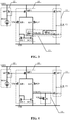
- FIGS. 1 to 5 are circuit diagrams of comparators according to some embodiments of the disclosure.
- a comparator of the present disclosure includes: a first-stage operational amplifier circuit 10, a second-stage operational amplifier circuit 11, a bias circuit 12, and a clamping circuit 13.
- the first-stage operational amplifier circuit 10 includes two voltage input terminals and one voltage output terminal; the two voltage input terminals of the first-stage operational amplifier circuit 10 are used for inputting the to-be-compared voltage; the second-stage operational amplifier circuit 11 is connected to the bias circuit 12 and the voltage output terminal of the first-stage operational amplifier circuit 10; the clamping circuit 13 is connected with the voltage output terminal of the first-stage operational amplifier circuit 10, and the clamping circuit 13 is used to connect the voltage output terminal of the first-stage operational amplifier circuit and clamp the highest voltage to the preset voltage.
- one input terminal of the first operational amplifier circuit 10 is used to input the first to-be-compared voltage VN, and the other input terminal of the first operational amplifier circuit 10 is used to input the second to-be-compared voltage VP.
- the first-stage operational amplifier circuit 10 includes: a first PMOS transistor MP1, a second PMOS transistor MP2, a third PMOS transistor MP3, a first NMOS transistor MN1, and a second NMOS transistor MN2.
- the gate of the first PMOS transistor MP1 is connected to the first to-be-compared voltage VN; the gate of the second PMOS transistor MP2 is connected to the second to-be-compared voltage VP; the gate of the third PMOS transistor MP3 is connected to the bias circuit 12, the drain of the third PMOS transistor MP3 is connected with the source of the first PMOS transistor MP1 and the source of the second PMOS transistor MP2; the gate and the drain of the first NMOS transistor MN1 are short-circuited, and connected to the drain of the first PMOS transistor MP1, the source of the first NMOS transistor MN1 is grounded; the gate of the second NMOS transistor MN2 is connected to the gate of the first NMOS transistor MN1, and the drain of the second NMOS transistor MN2 is connected to the drain of the second PMOS transistor MP2 to be the voltage output terminal of the first-stage operational amplifier circuit 10 for outputting the first output signal VOUT1, and the source of the second NMOS transistor MN2 is grounded.
- the second-stage operational amplifier circuit 11 includes: a fourth PMOS transistor MP4 and a third NMOS transistor MN3.
- the gate of the fourth PMOS transistor MP4 is connected to the bias circuit 12; the gate of the third NMOS transistor MN3 is connected to the voltage output terminal of the first-stage operational amplifier circuit 10, and the drain of the third NMOS transistor MN3 is connected to the drain of the fourth PMOS transistor MP4 to be as the voltage output terminal of the second-stage operational amplifier circuit 11, used for outputting the second output signal VOUT2, and the source of the third NMOS transistor MN3 is grounded.
- the bias circuit 12 includes: a fifth PMOS transistor MP5 and a current source IBIAS; wherein the gate of the fifth PMOS transistor MP5 is connected to the first-stage operational amplifier circuit 10 and the second-stage operational amplifier circuit 11.
- the gate and drain of the fifth PMOS transistor MP5 are connected to the current source IBIAS.
- the gate of the fifth PMOS transistor MP5 is connected to the gate of the third PMOS transistor MP3 and the gate of the fourth PMOS transistor MP4.
- the clamping circuit 13 may include a first switch transistor M, a control terminal and a current input terminal of the first switch transistor M are connected to a voltage output terminal of the first-stage operational amplifier circuit 10.
- the current output terminal of the first switch transistor M is connected to the gate of the second NMOS transistor MN2.
- the clamping circuit 13 can clamp the output terminal of the first-stage operational amplifier circuit 10, and can clamp the highest voltage of the output terminal of the first-stage operational amplifier circuit 10 to Vgs (gate-source voltage of the first switch transistor M) +Vgsn1 (the gate-source voltage of the first NMOS transistor MN1).
- the voltage VOUT1 at the output terminal of the first-stage operational amplifier circuit 10 will be no longer necessary to be pulled down from a high potential (VDD-Vonp3-Vonp2, where Vonp3 and Vonp2 are the conduction voltage values of the transistor MP3 and transistor MP2 respectively) to the ground potential, but be pulled down from a voltage of approximately Vgs+Vgsn1 (Vgs+Vgsn1 is less than VDD- Vonp3-Vonp2), so that the discharge delay to the first-stage operational amplifier circuit 10 is reduced, thereby increasing the flipping voltage of the comparator.
- the first-stage operational amplifier voltage 10 has a smaller change range, so the coupling effect of the change of the first-level operational amplifier circuit 10 on the first to-be-compared voltage VN and the second to-be-compared voltage VP is correspondingly reduced, and the first to-be-compared voltage VN and the second to-be-compared voltage VP are less interfered by kick back noise.
- the first switch transistor M may include an NMOS transistor.
- the clamping circuit 13 may include a first switch transistor M1, a control terminal and a current input terminal of the first switch transistor M1 are connected to a voltage output of the first-stage operational amplifier circuit 10.
- the current output terminal of the first switch transistor M1 is connected to the gate of the second NMOS transistor MN2; the control terminal and current input terminal of the second switch transistor M2 are connected to the voltage output terminal of the first-stage operational amplifier circuit 10.
- the current output terminal of the second switch transistor M2 is connected to the voltage output terminal of the second-stage operational amplifier circuit 11.
- the first switch transistor M1 may include an NMOS transistor
- the second switch transistor M2 may include an NMOS transistor
- the clamping circuit may include a switch transistor M.
- the control terminal and current input terminal of the switch transistor M are connected to the voltage output terminal of the first-stage operational amplifier circuit 10, and the current output terminal of the switch transistor M is connected to the output terminal of the second-stage operational amplifier circuit 11.
- the clamping circuit 13 can clamp the output terminal of the first-stage operational amplifier circuit 10, and can clamp the highest voltage of the output terminal of the first-stage operational amplifier circuit 10 to Vgs (the gate-source voltage of the switch transistor M) +Vdsn3 (the drain-source voltage of the third NMOS transistor MN3).
- the voltage VOUT1 at the output terminal of the first-stage operational amplifier circuit 10 will no longer need to be pulled down from a high potential (VDD-Vonp3-Vonp2, wherein Vonp3 and Vonp2 are conduction voltage values of the transistor MP3 and transistor MP2, respectively) to the ground potential, but instead be pulled down from a voltage of about Vgs+Vdsn3, so that the discharge delay of the first-stage operational amplifier circuit 10 is reduced, thereby increasing the flip voltage of the comparator.
- the change range of the voltage from the first-stage operational amplifier 10 is smaller, so the coupling effect from the change of the first-stage operational amplifier circuit 10 to the first to-be-compared voltage VN and the second to-be-compared voltage VP is also reduced accordingly, and thus the first to-be-compared voltage VN and the second to-be-compared voltage VP will be less interfered by any kick back noise.
- Vgsm1 is the gate-source voltage of the transistor M1
- Vgsn1 is the gate-source voltage of the transistor MN1
- Vgsm2+Vdsn3 Vgsm2 is the gate-source voltage of the transistor M2
- Vdsn3 is the drain-source voltage of the transistor MN3
- the switch transistor M may include an NMOS transistor.
- the clamping circuit 13 may include a switch transistor M.
- the current input terminal of the switch transistor M is connected to the voltage output terminal of the first-stage operational amplifier circuit 10.
- the control terminal of the switch transistor is connected with the bias voltage VBIAS, and the current output terminal of the switch transistor M is grounded.
- the clamping circuit 13 can clamp the output terminal of the first-stage operational amplifier circuit 10, and can clamp the highest voltage of the output terminal of the first-stage operational amplifier circuit 10 to Vgs1 (the gate-source voltage of the switch transistor M) +VBIAS.
- the voltage VOUT1 at the output terminal of the first-stage operational amplifier circuit 10 will no longer need to be pulled own from a high potential (VDD-Vonp3-Vonp2, wherein Vonp3 and Vonp2 are conduction voltage values of transistors MP3 and MP2 respectively) to the ground potential, but instead will be pulled down from a voltage of about Vgs1+VBIAS (Vgs1+VBIAS is less than VDD-Vonp3-Vonp2), and the clamped voltage of the output terminal of the first-stage operational amplifier circuit 10 may change by adjusting the VBIAS, so that the discharge delay from the first-stage operational amplifier circuit 10 is reduced, thereby increasing the flipping speed of the comparator.
- the change range of the voltage of the first-stage operational amplifier circuit 10 is smaller, so the coupling effect from the change of the first-stage operational amplifier circuit 10 to the first to-be-compared voltage VN and the second to-be-compared voltage VP is also reduced accordingly.
- the first to-be-compared voltage VN and the second to-be-compared voltage VP are less disturbed by kickback noise.
- the switch transistor M may include a PMOS transistor or a PNP type transistor.
- the clamping circuit 13 may include: a first switch transistor M1, a second switch transistor M2, and a third switch transistor M3; wherein, the current input terminal of the first switch transistor M1 is connected with the voltage output terminal of the first-stage operational amplifier circuit 10, the control terminal of the first switch transistor M1 is connected with the current output terminal of the second switch transistor M2 and the current input terminal of the third switch transistor M3; the control terminal of the second switch transistor M2 is connected to the bias circuit 12.
- the control terminal of the second switch transistor M2 is connected to the gate of the fifth PMOS transistor; the control terminal of the third switch transistor M3 is short-circuited with the current input terminal of the third switch transistor M3, and the circuit output terminal of the third switch transistor M3 is grounded.
- the bias voltage VBIAS connected to the gate of the first switch transistor M1 is the gate-source voltage of the third switch transistor M3.
- the first switch transistor M1, the second switch transistor M2, or the third switch transistor M3 are selected to have different transistor channel width-to-length ratios, and the clamping circuit 13 can be adjusted to clamp the voltage output terminal of the first-stage operational amplifier circuit 10 to a preset clamping voltage.
- the bias voltage VBIAS can be reduced, thereby reducing the clamping voltage; and by decreasing the channel width-to-length ratios of the first switch transistor M1, the second switch M2, or the third switch M3, the bias voltage VBIAS can be increased, thereby increasing the clamping voltage.
- the first switch transistor M1 includes a PMOS transistor or a PNP type transistor
- the second switch transistor M2 includes a PMOS transistor
- the third switch transistor M3 includes an NMOS transistor.
Landscapes
- Physics & Mathematics (AREA)
- Nonlinear Science (AREA)
- Manipulation Of Pulses (AREA)
- Amplifiers (AREA)
Abstract
Description
- This disclosure relates to the field of integrated circuit technology, and in particular, to a comparator.
- Existing comparators are widely used in electronics. One requirement for the comparators is to be able to quickly acquire the result of the comparison, so that the next step can be processed shortly. For example, when an over-current abnormality is detected, it is hoped that the abnormal situation can be handled as soon as possible. However, due to the inherent delay of the comparator itself, the processing speed is often lagging, and the flipping speed of the comparator is slow. This delay is mainly caused by charging and discharging delay at the output terminals of the first-stage operational amplifier circuit and the second-stage operational amplifier circuit in the comparator. For example, when the first to-be-compared voltage VP is greater than the second to-be-compared voltage VN, the output terminal of the first-stage operational amplifier the circuit will be pulled down from a higher potential to the ground potential. When the first to-be-compared voltage VP is less than the second to-be-compared voltage VN, the output terminal of the first-stage operational amplifier circuit will be pulled up to a high potential again. In addition, the rapid change of the output signal of the first-stage operational amplifier circuit in the comparator will be coupled to the first to-be-compared voltage VP, forming kick back noise, which will not only cause interference to the to-be-compared voltage, but may also cause output erroneous flip.
- Thus, it is necessary to overcome the problems in the existing techniques that comparators' processing speed lags from delays by the charging and discharging at the output terminals, slow turning speed, and kick back noise interfering with the comparison voltage, resulting in errors of flipping outputs, etc.
- An aspect of the present disclosure provides a comparator, including: a first-stage operational amplifier circuit, a second-stage operational amplifier circuit, a bias circuit and a clamping circuit.
- The first-stage operational amplifier circuit includes two voltage input terminals and one voltage output terminal; and the two voltage input terminals of the first-stage operational amplifier circuit are used for inputting voltages to-be-compared.
- The second-stage operational amplifier circuit is connected to the bias circuit and the voltage output terminal of the first-stage operational amplifier circuit.
- The clamping circuit is connected to the voltage output terminal of the first-stage operational amplifier circuit, and is used to clamp the highest voltage of the voltage output terminal of the first-stage operational amplifier circuit to a preset voltage.
- By adding a clamping circuit in the above-mentioned comparator, the highest voltage of the voltage output terminal of the first-stage operational amplifier circuit can be clamped to the preset voltage. During the operation of the comparator, the voltage changing range of the voltage output terminal of the first-stage operational amplifier circuit is relatively small, which can reduce the discharge delay of the voltage output terminal of the first-stage operational amplifier circuit, thereby improving the flip speed of the comparator. In addition, because the voltage change range of the output terminal of the first-stage operational amplifier circuit is relatively small, the coupling effect of the voltage change at the voltage output terminal of the first-stage operational amplifier circuit to the input to-be-compared voltage is also reduced accordingly, which can reduce the kick back noise of the input to-be-compared voltage, avoid interference to the to-be-compared voltage, and ensure the correctness of the output. At the same time, the above-mentioned comparator also has the advantages of having a simple structure, a low cost and easy implementation.
- In some embodiments, the first-stage operational amplifier circuit includes: a first PMOS transistor, a second PMOS transistor, a third PMOS transistor, a first NMOS transistor, and a second NMOS transistor. The gate of the first PMOS transistor is connected to the first to-be-compared voltage; the gate of the second PMOS transistor is connected to the second to-be-compared voltage; the gate of the third PMOS transistor is connected to the bias circuit, and the drain of the third PMOS transistor is connected to the source of the first PMOS transistor and the source of the second PMOS transistor; the gate and drain of the first NMOS transistor are short-circuited and connected to the drain of the first PMOS transistor, and the source of the first NMOS transistor is grounded; the gate of the second NMOS transistor is connected to the gate of the first NMOS transistor, and the drain of the second NMOS transistor is connected to the drain of the second PMOS transistor to be the output terminal of the first-stage operational amplifier circuit, and the source of the second NMOS transistor is grounded.
- In some embodiments, the clamping circuit includes a first switch transistor, where the control terminal and the current input terminal of the first switch transistor are connected to the voltage output terminal of the first-stage operational amplifier circuit, and the current output terminal of the first switch transistor is connected with the gate of the second NMOS.
- In some embodiments, the first switch transistor includes an NMOS transistor.
- In some embodiments, the clamping circuit further includes a second switch transistor, where the control terminal and current input terminal of the second switch transistor are connected to the voltage output terminal of the first-stage operational amplifier circuit, and the current output terminal of the second switch transistor is connected with the voltage output terminal of the second-stage operational amplifier circuit.
- In some examples, the second-stage operational amplifier circuit includes: a fourth PMOS transistor and a third NMOS transistor; wherein, the gate of the fourth PMOS transistor is connected to the bias circuit; the gate of the third NMOS transistor is connected to the voltage output terminal of the first-stage operational amplifier circuit, and the drain of the third NMOS transistor is connected to the drain of the fourth PMOS transistor as the voltage output terminal of the second-stage operational amplifier circuit, and the source of the third NMOS transistor is grounded.
- In some examples, the bias circuit includes: a fifth PMOS transistor and a current source; wherein, the gate of the fifth PMOS transistor is connected to the first-stage operational amplifier circuit and the second-stage operational amplifier circuit, and the drain of the fifth PMOS transistor is connected to the current source.
- In some embodiments, the clamping circuit includes a switch transistor, where the control terminal and current input terminal of the switch transistor are connected to the voltage output terminal of the first-stage operational amplifier circuit, and the current output terminal of the switch transistor is connected with the output terminal of the second-stage operational amplifier circuit.
- In some embodiments, the switch transistor includes an NMOS transistor.
- In some embodiments, the clamping circuit includes a switch transistor, where the current input terminal of the switch transistor is connected to the voltage output terminal of the first-stage operational amplifier circuit, the control terminal of the switch transistor is connected to the bias voltage, and the current output terminal of the switch transistor is grounded.
- In some embodiments, the switch transistor includes a PMOS transistor or a PNP type transistor.
- In some embodiments, the clamping circuit includes: a first switch transistor, a second switch transistor, and a third switch transistor; wherein, the current input terminal of the first switch transistor is connected to the voltage output terminal of the first-stage operational amplifier circuit, and the control terminal of the first switch transistor is connected to the current output terminal of the second switch transistor and the current input terminal of the three switch transistor; the control terminal of the second switch transistor is connected to the bias circuit; the control terminal of the third switch transistor is short-circuited with the current input terminal of the third switch transistor, and the circuit output terminal of the third switch transistor is grounded.
- In some embodiments, the first switch transistor includes a PMOS transistor or a PNP type transistor, the second switch transistor includes a PMOS transistor, and the third switch transistor includes an NMOS transistor.
-
FIGS. 1 to 5 are circuit diagrams of comparators according to some embodiments of the disclosure. - Description of reference numerals:
- 10
- The first-stage operational amplifier circuit
- 11
- The second-stage operational amplifier circuit
- 12
- Bias circuit
- 13
- Clamping circuit
- In order to facilitate the understanding of the present disclosure, the following will make a more comprehensive description of the present disclosure with reference to the relevant drawings. The preferred embodiment of the present disclosure is shown in the accompanying drawings. However, the present disclosure can be implemented in many different forms and is not limited to the embodiments described herein. On the contrary, the purpose of providing these embodiments is to make the disclosure of the present disclosure more thorough and comprehensive.
- It should be noted that when an element is considered to be "connected" to another element, it may be directly connected to and integrated with another element, or there may be a centering element at the same time. The terms "installed", "one terminal", "the other terminal" and similar expressions used herein are for illustrative purposes only.
- Unless otherwise defined, all technical and scientific terms used herein have the same meaning as commonly understood by those skilled in the technical field of the present disclosure. The terminology used in the specification of the present disclosure herein is only for the purpose of describing specific embodiments, and is not intended to limit the present disclosure. The term "and/or" as used herein includes any and all combinations of one or more related listed items.
- In one embodiment, as shown in
FIGS. 1 to 5 , a comparator of the present disclosure includes: a first-stageoperational amplifier circuit 10, a second-stageoperational amplifier circuit 11, abias circuit 12, and aclamping circuit 13. The first-stageoperational amplifier circuit 10 includes two voltage input terminals and one voltage output terminal; the two voltage input terminals of the first-stageoperational amplifier circuit 10 are used for inputting the to-be-compared voltage; the second-stageoperational amplifier circuit 11 is connected to thebias circuit 12 and the voltage output terminal of the first-stageoperational amplifier circuit 10; theclamping circuit 13 is connected with the voltage output terminal of the first-stageoperational amplifier circuit 10, and theclamping circuit 13 is used to connect the voltage output terminal of the first-stage operational amplifier circuit and clamp the highest voltage to the preset voltage. - Specifically, one input terminal of the first
operational amplifier circuit 10 is used to input the first to-be-compared voltage VN, and the other input terminal of the firstoperational amplifier circuit 10 is used to input the second to-be-compared voltage VP. - In an example, continue to refer to
FIGS. 1 to 5 , the first-stageoperational amplifier circuit 10 includes: a first PMOS transistor MP1, a second PMOS transistor MP2, a third PMOS transistor MP3, a first NMOS transistor MN1, and a second NMOS transistor MN2. The gate of the first PMOS transistor MP1 is connected to the first to-be-compared voltage VN; the gate of the second PMOS transistor MP2 is connected to the second to-be-compared voltage VP; the gate of the third PMOS transistor MP3 is connected to thebias circuit 12, the drain of the third PMOS transistor MP3 is connected with the source of the first PMOS transistor MP1 and the source of the second PMOS transistor MP2; the gate and the drain of the first NMOS transistor MN1 are short-circuited, and connected to the drain of the first PMOS transistor MP1, the source of the first NMOS transistor MN1 is grounded; the gate of the second NMOS transistor MN2 is connected to the gate of the first NMOS transistor MN1, and the drain of the second NMOS transistor MN2 is connected to the drain of the second PMOS transistor MP2 to be the voltage output terminal of the first-stageoperational amplifier circuit 10 for outputting the first output signal VOUT1, and the source of the second NMOS transistor MN2 is grounded. - In an example, the second-stage
operational amplifier circuit 11 includes: a fourth PMOS transistor MP4 and a third NMOS transistor MN3. The gate of the fourth PMOS transistor MP4 is connected to thebias circuit 12; the gate of the third NMOS transistor MN3 is connected to the voltage output terminal of the first-stageoperational amplifier circuit 10, and the drain of the third NMOS transistor MN3 is connected to the drain of the fourth PMOS transistor MP4 to be as the voltage output terminal of the second-stageoperational amplifier circuit 11, used for outputting the second output signal VOUT2, and the source of the third NMOS transistor MN3 is grounded. - In an example, the
bias circuit 12 includes: a fifth PMOS transistor MP5 and a current source IBIAS; wherein the gate of the fifth PMOS transistor MP5 is connected to the first-stageoperational amplifier circuit 10 and the second-stageoperational amplifier circuit 11. The gate and drain of the fifth PMOS transistor MP5 are connected to the current source IBIAS. Specifically, the gate of the fifth PMOS transistor MP5 is connected to the gate of the third PMOS transistor MP3 and the gate of the fourth PMOS transistor MP4. - In an example, as shown in
FIG. 1 , the clampingcircuit 13 may include a first switch transistor M, a control terminal and a current input terminal of the first switch transistor M are connected to a voltage output terminal of the first-stageoperational amplifier circuit 10. The current output terminal of the first switch transistor M is connected to the gate of the second NMOS transistor MN2. In this example, the clampingcircuit 13 can clamp the output terminal of the first-stageoperational amplifier circuit 10, and can clamp the highest voltage of the output terminal of the first-stageoperational amplifier circuit 10 to Vgs (gate-source voltage of the first switch transistor M) +Vgsn1 (the gate-source voltage of the first NMOS transistor MN1). In this way, when the second to-be-compared voltage VP is greater than the first to-be-compared voltage VN, the voltage VOUT1 at the output terminal of the first-stageoperational amplifier circuit 10 will be no longer necessary to be pulled down from a high potential (VDD-Vonp3-Vonp2, where Vonp3 and Vonp2 are the conduction voltage values of the transistor MP3 and transistor MP2 respectively) to the ground potential, but be pulled down from a voltage of approximately Vgs+Vgsn1 (Vgs+Vgsn1 is less than VDD- Vonp3-Vonp2), so that the discharge delay to the first-stageoperational amplifier circuit 10 is reduced, thereby increasing the flipping voltage of the comparator. At the same time, the first-stageoperational amplifier voltage 10 has a smaller change range, so the coupling effect of the change of the first-leveloperational amplifier circuit 10 on the first to-be-compared voltage VN and the second to-be-compared voltage VP is correspondingly reduced, and the first to-be-compared voltage VN and the second to-be-compared voltage VP are less interfered by kick back noise. - In an example, the first switch transistor M may include an NMOS transistor.
- In another optional example, as shown in
FIG. 3 , the clampingcircuit 13 may include a first switch transistor M1, a control terminal and a current input terminal of the first switch transistor M1 are connected to a voltage output of the first-stageoperational amplifier circuit 10. The current output terminal of the first switch transistor M1 is connected to the gate of the second NMOS transistor MN2; the control terminal and current input terminal of the second switch transistor M2 are connected to the voltage output terminal of the first-stageoperational amplifier circuit 10. The current output terminal of the second switch transistor M2 is connected to the voltage output terminal of the second-stageoperational amplifier circuit 11. - In an example, the first switch transistor M1 may include an NMOS transistor, and the second switch transistor M2 may include an NMOS transistor.
- In yet another optional example, as shown in
FIG. 2 , the clamping circuit may include a switch transistor M. The control terminal and current input terminal of the switch transistor M are connected to the voltage output terminal of the first-stageoperational amplifier circuit 10, and the current output terminal of the switch transistor M is connected to the output terminal of the second-stageoperational amplifier circuit 11. In this example, the clampingcircuit 13 can clamp the output terminal of the first-stageoperational amplifier circuit 10, and can clamp the highest voltage of the output terminal of the first-stageoperational amplifier circuit 10 to Vgs (the gate-source voltage of the switch transistor M) +Vdsn3 (the drain-source voltage of the third NMOS transistor MN3). In this way, when the second to-be-compared voltage VP is greater than the first to-be-compared voltage VN, the voltage VOUT1 at the output terminal of the first-stageoperational amplifier circuit 10 will no longer need to be pulled down from a high potential (VDD-Vonp3-Vonp2, wherein Vonp3 and Vonp2 are conduction voltage values of the transistor MP3 and transistor MP2, respectively) to the ground potential, but instead be pulled down from a voltage of about Vgs+Vdsn3, so that the discharge delay of the first-stageoperational amplifier circuit 10 is reduced, thereby increasing the flip voltage of the comparator. At the same time, the change range of the voltage from the first-stageoperational amplifier 10 is smaller, so the coupling effect from the change of the first-stageoperational amplifier circuit 10 to the first to-be-compared voltage VN and the second to-be-compared voltage VP is also reduced accordingly, and thus the first to-be-compared voltage VN and the second to-be-compared voltage VP will be less interfered by any kick back noise. - Returning to the structure of
FIG. 3 , combined with the analysis ofFIGS. 1 and 2 , it shows that the voltage VOUT1 at the output terminal of the first-stageoperational amplifier circuit 10 is clamped to be at the smaller value between Vgsm1+Vgsn1 (Vgsm1 is the gate-source voltage of the transistor M1, and Vgsn1 is the gate-source voltage of the transistor MN1) and Vgsm2+Vdsn3 (Vgsm2 is the gate-source voltage of the transistor M2, and Vdsn3 is the drain-source voltage of the transistor MN3), which further reduces the change range of the voltage VOUT1 at the output terminal of the first-stageoperational amplifier circuit 10, therefore it further increases the flipping speed of the comparator and reduces its kick back noise. - In an example, the switch transistor M may include an NMOS transistor.
- In yet another example, as shown in
FIG. 4 , the clampingcircuit 13 may include a switch transistor M. The current input terminal of the switch transistor M is connected to the voltage output terminal of the first-stageoperational amplifier circuit 10. The control terminal of the switch transistor is connected with the bias voltage VBIAS, and the current output terminal of the switch transistor M is grounded. In this example, the clampingcircuit 13 can clamp the output terminal of the first-stageoperational amplifier circuit 10, and can clamp the highest voltage of the output terminal of the first-stageoperational amplifier circuit 10 to Vgs1 (the gate-source voltage of the switch transistor M) +VBIAS. In this way, when the second to-be-compared voltage VP is greater than the first to-be-compared voltage VN, the voltage VOUT1 at the output terminal of the first-stageoperational amplifier circuit 10 will no longer need to be pulled own from a high potential (VDD-Vonp3-Vonp2, wherein Vonp3 and Vonp2 are conduction voltage values of transistors MP3 and MP2 respectively) to the ground potential, but instead will be pulled down from a voltage of about Vgs1+VBIAS (Vgs1+VBIAS is less than VDD-Vonp3-Vonp2), and the clamped voltage of the output terminal of the first-stageoperational amplifier circuit 10 may change by adjusting the VBIAS, so that the discharge delay from the first-stageoperational amplifier circuit 10 is reduced, thereby increasing the flipping speed of the comparator. At the same time, the change range of the voltage of the first-stageoperational amplifier circuit 10 is smaller, so the coupling effect from the change of the first-stageoperational amplifier circuit 10 to the first to-be-compared voltage VN and the second to-be-compared voltage VP is also reduced accordingly. The first to-be-compared voltage VN and the second to-be-compared voltage VP are less disturbed by kickback noise. - In an example, the switch transistor M may include a PMOS transistor or a PNP type transistor.
- In another example, as shown in
FIG. 5 , the clampingcircuit 13 may include: a first switch transistor M1, a second switch transistor M2, and a third switch transistor M3; wherein, the current input terminal of the first switch transistor M1 is connected with the voltage output terminal of the first-stageoperational amplifier circuit 10, the control terminal of the first switch transistor M1 is connected with the current output terminal of the second switch transistor M2 and the current input terminal of the third switch transistor M3; the control terminal of the second switch transistor M2 is connected to thebias circuit 12. Specifically, the control terminal of the second switch transistor M2 is connected to the gate of the fifth PMOS transistor; the control terminal of the third switch transistor M3 is short-circuited with the current input terminal of the third switch transistor M3, and the circuit output terminal of the third switch transistor M3 is grounded. In this example, the bias voltage VBIAS connected to the gate of the first switch transistor M1 is the gate-source voltage of the third switch transistor M3. The first switch transistor M1, the second switch transistor M2, or the third switch transistor M3 are selected to have different transistor channel width-to-length ratios, and the clampingcircuit 13 can be adjusted to clamp the voltage output terminal of the first-stageoperational amplifier circuit 10 to a preset clamping voltage. For example, by increasing the channel width-to-length ratios of the first switch transistor M1, the second switch M2, or the third switch M3, the bias voltage VBIAS can be reduced, thereby reducing the clamping voltage; and by decreasing the channel width-to-length ratios of the first switch transistor M1, the second switch M2, or the third switch M3, the bias voltage VBIAS can be increased, thereby increasing the clamping voltage. - In an example, the first switch transistor M1 includes a PMOS transistor or a PNP type transistor, the second switch transistor M2 includes a PMOS transistor, and the third switch transistor M3 includes an NMOS transistor.
- The technical features of the above-mentioned embodiments can be combined arbitrarily. In order to make the description concise, not all possible combinations of the technical features of the above-mentioned embodiments are described. However, as long as there is no contradiction in the combination of these technical features, they should be It is considered as the range described in this specification.
- The above-mentioned embodiments only express several implementation modes of the present disclosure, and their descriptions are relatively specific and detailed, but they should not be understood as limiting the scope of the present disclosure. It should be pointed out that for those of ordinary skill in the art, without departing from the concept of the present disclosure, several modifications and improvements can be made, and these all fall within the protection scope of the present disclosure. Therefore, the scope of protection of the patent in the present disclosure shall be subject to the appended claims.
Claims (13)
- A comparator, comprising: a first-stage operational amplifier circuit, a second-stage operational amplifier circuit, a bias circuit, and a clamping circuit;wherein the first-stage operational amplifier circuit comprises two voltage input terminals and a voltage output terminal, wherein the two voltage input terminals input two to-be-compared voltages respectively;wherein the second-stage operational amplifier circuit is connected to the bias circuit and the voltage output terminal of the first-stage operational amplifier circuit; andwherein the clamping circuit is connected to the voltage output terminal of the first-stage operational amplifier circuit, and clamps a highest voltage from the voltage output terminal of the first-stage operational amplifier circuit to a preset voltage.
- The comparator according to claim 1, wherein the first-stage operational amplifier circuit further comprises: a first positive channel Metal Oxide Semiconductor (PMOS) transistor, a second PMOS transistor, a third PMOS transistor, a first negative channel Metal Oxide Semiconductor (NMOS) transistor, and a second NMOS transistor;wherein a gate of the first PMOS transistor is connected to a first to-be-compared voltage;wherein a gate of the second PMOS transistor is connected to a second to-be-compared voltage;wherein a gate of the third PMOS transistor is connected to the bias circuit, and a drain of the third PMOS transistor is connected to a source of the first PMOS transistor and a source of the second PMOS transistor;wherein a gate and a drain of the first NMOS transistor are short-circuited and connected to a drain of the first PMOS transistor, and wherein a source of the first NMOS transistor is grounded;wherein a gate of the second NMOS transistor is connected to a gate of the first NMOS transistor, and a drain of the second NMOS transistor is connected to a drain of the second PMOS transistor as the voltage output terminal of the first-stage operational amplifier circuit; and wherein a source of the second NMOS transistor is grounded.
- The comparator according to claim 2, wherein the clamping circuit comprises a first switch transistor, and wherein a control terminal and a current input terminal of the first switch transistor are connected to the voltage output terminal of the first-stage operational amplifier circuit, and a current output terminal of the first switch transistor is connected to the gate of the second NMOS transistor.
- The comparator according to claim 3, wherein the first switch transistor comprises an NMOS transistor.
- The comparator according to claim 3, wherein the clamping circuit further comprises a second switch transistor, wherein a control terminal and a current input terminal of the second switch transistor are connected to the voltage output terminal of the first-stage operational amplifier circuit, and a current output terminal of the second switch transistor is connected to a voltage output terminal of the second-stage operational amplifier circuit.
- The comparator according to claim 1, wherein the second-stage operational amplifier circuit further comprises: a fourth PMOS transistor and a third NMOS transistor;wherein a gate of the fourth PMOS transistor is connected to the bias circuit;wherein a gate of the third NMOS transistor is connected to the voltage output terminal of the first-stage operational amplifier circuit;wherein a drain of the third NMOS transistor is connected to a drain of the fourth PMOS transistor as a voltage output terminal of the second-stage operational amplifier circuit; and a source of the third NMOS transistor is grounded.
- The comparator according to claim 1, wherein the bias circuit comprises: a fifth PMOS transistor and a current source;
wherein a gate of the fifth PMOS transistor is connected to the first-stage operational amplifier circuit and the second-stage operational amplifier circuit, and wherein a drain of the fifth PMOS transistor is connected to the current source. - The comparator according to claim 1, 2, 6 or 7, wherein the clamping circuit comprises a switch transistor, wherein a control terminal and a current input terminal of the switch transistor are connected to the voltage output terminal of the first-stage operational amplifier circuit, and wherein a current output terminal of the switch transistor is connected with a voltage output terminal of the second-stage operational amplifier circuit.
- The comparator according to claim 8, wherein the switch transistor comprises an NMOS transistor.
- The comparator according to claim 1, 2, 6 or 7, wherein the clamping circuit comprises a switch transistor, wherein a current input terminal of the switch transistor is connected to the voltage output terminal of the first-stage operational amplifier circuit, a control terminal of the switch transistor is connected with a bias voltage of the bias circuit, and a current output terminal of the switch transistor is grounded.
- The comparator according to claim 10, wherein the switch transistor comprises a PMOS transistor or a PNP type transistor.
- The comparator according to claim 1, 2, 6 or 7, wherein the clamping circuit comprises: a first switch transistor, a second switch transistor, and a third switch transistor;wherein a current input terminal of the first switch transistor is connected to the voltage output terminal of the first-stage operational amplifier circuit, and a control terminal of the first switch transistor, a current output terminal of the second switch transistor, and a current input terminal of the third switch transistor are connected;wherein a control terminal of the second switch transistor is connected to the bias circuit;wherein a control terminal of the third switch transistor is short-circuited with the current input terminal of the third switch transistor; and an output terminal of the third switch transistor is grounded.
- The comparator according to claim 12, wherein the first switch transistor comprises a PMOS transistor or a PNP type transistor, the second switch transistor comprises a PMOS transistor, and the third switch transistor comprises an NMOS transistor.
Applications Claiming Priority (2)
| Application Number | Priority Date | Filing Date | Title |
|---|---|---|---|
| CN201911188793.3A CN112865763B (en) | 2019-11-28 | 2019-11-28 | Comparator |
| PCT/CN2020/097020 WO2021103500A1 (en) | 2019-11-28 | 2020-06-19 | Comparator |
Publications (2)
| Publication Number | Publication Date |
|---|---|
| EP3923473A1 true EP3923473A1 (en) | 2021-12-15 |
| EP3923473A4 EP3923473A4 (en) | 2022-06-15 |
Family
ID=75985227
Family Applications (1)
| Application Number | Title | Priority Date | Filing Date |
|---|---|---|---|
| EP20892667.5A Withdrawn EP3923473A4 (en) | 2019-11-28 | 2020-06-19 | COMPARATOR |
Country Status (4)
| Country | Link |
|---|---|
| US (1) | US11683027B2 (en) |
| EP (1) | EP3923473A4 (en) |
| CN (1) | CN112865763B (en) |
| WO (1) | WO2021103500A1 (en) |
Families Citing this family (5)
| Publication number | Priority date | Publication date | Assignee | Title |
|---|---|---|---|---|
| CN115362631A (en) * | 2020-03-30 | 2022-11-18 | 罗姆股份有限公司 | Comparator circuit |
| FR3117288B1 (en) * | 2020-12-09 | 2023-05-26 | Commissariat Energie Atomique | Dynamic comparator |
| DE112021006258T5 (en) * | 2021-02-03 | 2023-09-14 | Rohm Co., Ltd. | POWER SUPPLY DEVICE |
| CN113644901B (en) * | 2021-10-14 | 2022-01-18 | 南京模砾半导体有限责任公司 | High-speed comparator circuit |
| JP2023172381A (en) * | 2022-05-23 | 2023-12-06 | 日清紡マイクロデバイス株式会社 | differential amplifier circuit |
Family Cites Families (20)
| Publication number | Priority date | Publication date | Assignee | Title |
|---|---|---|---|---|
| US4443717A (en) * | 1980-01-14 | 1984-04-17 | American Microsystems, Inc. | High resolution fast diode clamped comparator |
| US5541538A (en) * | 1994-09-01 | 1996-07-30 | Harris Corporation | High speed comparator |
| JPH09321586A (en) * | 1996-05-29 | 1997-12-12 | Toshiba Microelectron Corp | Level comparator |
| JP2001053558A (en) * | 1999-08-09 | 2001-02-23 | Nippon Telegr & Teleph Corp <Ntt> | Operational amplifier |
| JP3855810B2 (en) * | 2002-03-14 | 2006-12-13 | 株式会社デンソー | Differential amplifier circuit |
| US7233174B2 (en) * | 2004-07-19 | 2007-06-19 | Texas Instruments Incorporated | Dual polarity, high input voltage swing comparator using MOS input transistors |
| JP2006352193A (en) * | 2005-06-13 | 2006-12-28 | Seiko Instruments Inc | Differential amplifier |
| US8031498B2 (en) * | 2007-07-05 | 2011-10-04 | Infineon Technologies Austria Ag | Active diode |
| JP2009159508A (en) * | 2007-12-27 | 2009-07-16 | Nec Electronics Corp | Operational amplifier and integrating circuit |
| TW201223137A (en) * | 2010-11-25 | 2012-06-01 | Novatek Microelectronics Corp | Operational amplifier and display driving circuit using the same |
| US8441319B2 (en) * | 2011-06-17 | 2013-05-14 | Analog Devices, Inc. | Method and apparatus for biasing rail to rail DMOS amplifier output stage |
| CN102420594B (en) * | 2011-12-15 | 2016-03-16 | 无锡中感微电子股份有限公司 | A kind of comparator |
| KR101965632B1 (en) * | 2012-09-07 | 2019-04-05 | 삼성전자 주식회사 | Correlated Double Sampling Circuit, Image Sensor including the Same, And Method there-of |
| EP2747284B1 (en) * | 2012-12-20 | 2016-05-25 | Stichting IMEC Nederland | An active diode circuit |
| JP6376874B2 (en) | 2014-01-21 | 2018-08-22 | エイブリック株式会社 | Amplifier circuit |
| CN104090619A (en) | 2014-07-18 | 2014-10-08 | 周国文 | Digital-analog hybrid circuit reference source with high work stability |
| CN104158517B (en) | 2014-08-26 | 2016-08-31 | 深圳市华星光电技术有限公司 | Comparator |
| CN205720085U (en) | 2016-05-10 | 2016-11-23 | 泛测(北京)环境科技有限公司 | A kind of amplifying circuit for tiny signal for air quality electrochemical sensor |
| US9917594B1 (en) * | 2016-09-06 | 2018-03-13 | Texas Instruments Incorporated | Inbuilt threshold comparator |
| CN210578470U (en) * | 2019-11-28 | 2020-05-19 | 长鑫存储技术有限公司 | Comparator with a comparator circuit |
-
2019
- 2019-11-28 CN CN201911188793.3A patent/CN112865763B/en active Active
-
2020
- 2020-06-19 WO PCT/CN2020/097020 patent/WO2021103500A1/en not_active Ceased
- 2020-06-19 EP EP20892667.5A patent/EP3923473A4/en not_active Withdrawn
- 2020-06-19 US US17/287,496 patent/US11683027B2/en active Active
Also Published As
| Publication number | Publication date |
|---|---|
| US11683027B2 (en) | 2023-06-20 |
| CN112865763B (en) | 2025-02-07 |
| WO2021103500A1 (en) | 2021-06-03 |
| EP3923473A4 (en) | 2022-06-15 |
| CN112865763A (en) | 2021-05-28 |
| US20220311429A1 (en) | 2022-09-29 |
Similar Documents
| Publication | Publication Date | Title |
|---|---|---|
| US11683027B2 (en) | Comparators | |
| CN210578470U (en) | Comparator with a comparator circuit | |
| US7154294B2 (en) | Comparators capable of output offset calibration | |
| CN107085132B (en) | A kind of high-precision detection of negative pressure circuit under positive voltage power supply | |
| US8264277B2 (en) | Differential amplifier circuit | |
| US5115151A (en) | Triple comparator circuit | |
| US20150146884A1 (en) | Circuit for suppressing audio output noise and audio output circuit | |
| CN211405974U (en) | Electronic device and system for squelch detection | |
| US20180367131A1 (en) | High voltage comparator | |
| US8542139B2 (en) | Current switch driving circuit and digital to analog converter | |
| CN112825474A (en) | High linearity input buffer | |
| CN111416579B (en) | Receiver front-end circuit and operation method thereof | |
| TWI558112B (en) | Squelch detector | |
| CN111865274B (en) | Comparator circuit | |
| US9360505B1 (en) | Squelch detector | |
| US20070064953A1 (en) | Speaker protection circuit | |
| US10627838B1 (en) | Comparator with adaptive sense voltage clamp | |
| US10819289B1 (en) | Signal processing circuit | |
| US20140167850A1 (en) | Current feedback output circuit | |
| US10622956B2 (en) | Signal level detection and overrange signal limiter and clamp for electronic circuits | |
| CN105024698B (en) | Voltage sensing circuit | |
| US9383391B2 (en) | Voltage sensing circuit | |
| TW201644188A (en) | Balanced differential transimpedance amplifier with single ended input and balancing method | |
| US20250085731A1 (en) | Constant voltage generator circuit operating at low voltage potential difference between input voltage and output voltage | |
| CN101154930A (en) | Automatic Gain Control Circuit |
Legal Events
| Date | Code | Title | Description |
|---|---|---|---|
| STAA | Information on the status of an ep patent application or granted ep patent |
Free format text: STATUS: THE INTERNATIONAL PUBLICATION HAS BEEN MADE |
|
| PUAI | Public reference made under article 153(3) epc to a published international application that has entered the european phase |
Free format text: ORIGINAL CODE: 0009012 |
|
| STAA | Information on the status of an ep patent application or granted ep patent |
Free format text: STATUS: REQUEST FOR EXAMINATION WAS MADE |
|
| 17P | Request for examination filed |
Effective date: 20210907 |
|
| AK | Designated contracting states |
Kind code of ref document: A1 Designated state(s): AL AT BE BG CH CY CZ DE DK EE ES FI FR GB GR HR HU IE IS IT LI LT LU LV MC MK MT NL NO PL PT RO RS SE SI SK SM TR |
|
| A4 | Supplementary search report drawn up and despatched |
Effective date: 20220516 |
|
| RIC1 | Information provided on ipc code assigned before grant |
Ipc: H03K 5/24 20060101AFI20220510BHEP |
|
| STAA | Information on the status of an ep patent application or granted ep patent |
Free format text: STATUS: EXAMINATION IS IN PROGRESS |
|
| DAV | Request for validation of the european patent (deleted) | ||
| DAX | Request for extension of the european patent (deleted) | ||
| 17Q | First examination report despatched |
Effective date: 20230223 |
|
| STAA | Information on the status of an ep patent application or granted ep patent |
Free format text: STATUS: THE APPLICATION IS DEEMED TO BE WITHDRAWN |
|
| 18D | Application deemed to be withdrawn |
Effective date: 20240611 |