EP3923459A1 - Rectifier for piezoelectric energy harvesting, piezoelectric energy harvester and associated method - Google Patents

Rectifier for piezoelectric energy harvesting, piezoelectric energy harvester and associated method Download PDF

Info

Publication number
EP3923459A1
EP3923459A1 EP20178812.2A EP20178812A EP3923459A1 EP 3923459 A1 EP3923459 A1 EP 3923459A1 EP 20178812 A EP20178812 A EP 20178812A EP 3923459 A1 EP3923459 A1 EP 3923459A1
Authority
EP
European Patent Office
Prior art keywords
terminal
switch
voltage
regulator
active diode
Prior art date
Legal status (The legal status is an assumption and is not a legal conclusion. Google has not performed a legal analysis and makes no representation as to the accuracy of the status listed.)
Withdrawn
Application number
EP20178812.2A
Other languages
German (de)
French (fr)
Inventor
Vincent Frick
Current Assignee (The listed assignees may be inaccurate. Google has not performed a legal analysis and makes no representation or warranty as to the accuracy of the list.)
Centre National de la Recherche Scientifique CNRS
Universite de Strasbourg
Original Assignee
Centre National de la Recherche Scientifique CNRS
Universite de Strasbourg
Priority date (The priority date is an assumption and is not a legal conclusion. Google has not performed a legal analysis and makes no representation as to the accuracy of the date listed.)
Filing date
Publication date
Application filed by Centre National de la Recherche Scientifique CNRS, Universite de Strasbourg filed Critical Centre National de la Recherche Scientifique CNRS
Priority to EP20178812.2A priority Critical patent/EP3923459A1/en
Priority to PCT/EP2021/065130 priority patent/WO2021249919A1/en
Publication of EP3923459A1 publication Critical patent/EP3923459A1/en
Withdrawn legal-status Critical Current

Links

Images

Classifications

    • HELECTRICITY
    • H02GENERATION; CONVERSION OR DISTRIBUTION OF ELECTRIC POWER
    • H02MAPPARATUS FOR CONVERSION BETWEEN AC AND AC, BETWEEN AC AND DC, OR BETWEEN DC AND DC, AND FOR USE WITH MAINS OR SIMILAR POWER SUPPLY SYSTEMS; CONVERSION OF DC OR AC INPUT POWER INTO SURGE OUTPUT POWER; CONTROL OR REGULATION THEREOF
    • H02M7/00Conversion of AC power input into DC power output; Conversion of DC power input into AC power output
    • H02M7/02Conversion of AC power input into DC power output without possibility of reversal
    • H02M7/04Conversion of AC power input into DC power output without possibility of reversal by static converters
    • H02M7/12Conversion of AC power input into DC power output without possibility of reversal by static converters using discharge tubes with control electrode or semiconductor devices with control electrode
    • H02M7/21Conversion of AC power input into DC power output without possibility of reversal by static converters using discharge tubes with control electrode or semiconductor devices with control electrode using devices of a triode or transistor type requiring continuous application of a control signal
    • H02M7/217Conversion of AC power input into DC power output without possibility of reversal by static converters using discharge tubes with control electrode or semiconductor devices with control electrode using devices of a triode or transistor type requiring continuous application of a control signal using semiconductor devices only
    • H02M7/219Conversion of AC power input into DC power output without possibility of reversal by static converters using discharge tubes with control electrode or semiconductor devices with control electrode using devices of a triode or transistor type requiring continuous application of a control signal using semiconductor devices only in a bridge configuration
    • HELECTRICITY
    • H02GENERATION; CONVERSION OR DISTRIBUTION OF ELECTRIC POWER
    • H02NELECTRIC MACHINES NOT OTHERWISE PROVIDED FOR
    • H02N2/00Electric machines in general using piezoelectric effect, electrostriction or magnetostriction
    • H02N2/18Electric machines in general using piezoelectric effect, electrostriction or magnetostriction producing electrical output from mechanical input, e.g. generators
    • H02N2/181Circuits; Control arrangements or methods
    • HELECTRICITY
    • H02GENERATION; CONVERSION OR DISTRIBUTION OF ELECTRIC POWER
    • H02MAPPARATUS FOR CONVERSION BETWEEN AC AND AC, BETWEEN AC AND DC, OR BETWEEN DC AND DC, AND FOR USE WITH MAINS OR SIMILAR POWER SUPPLY SYSTEMS; CONVERSION OF DC OR AC INPUT POWER INTO SURGE OUTPUT POWER; CONTROL OR REGULATION THEREOF
    • H02M1/00Details of apparatus for conversion
    • H02M1/0045Converters combining the concepts of switch-mode regulation and linear regulation, e.g. linear pre-regulator to switching converter, linear and switching converter in parallel, same converter or same transistor operating either in linear or switching mode
    • HELECTRICITY
    • H02GENERATION; CONVERSION OR DISTRIBUTION OF ELECTRIC POWER
    • H02MAPPARATUS FOR CONVERSION BETWEEN AC AND AC, BETWEEN AC AND DC, OR BETWEEN DC AND DC, AND FOR USE WITH MAINS OR SIMILAR POWER SUPPLY SYSTEMS; CONVERSION OF DC OR AC INPUT POWER INTO SURGE OUTPUT POWER; CONTROL OR REGULATION THEREOF
    • H02M1/00Details of apparatus for conversion
    • H02M1/0048Circuits or arrangements for reducing losses
    • HELECTRICITY
    • H02GENERATION; CONVERSION OR DISTRIBUTION OF ELECTRIC POWER
    • H02MAPPARATUS FOR CONVERSION BETWEEN AC AND AC, BETWEEN AC AND DC, OR BETWEEN DC AND DC, AND FOR USE WITH MAINS OR SIMILAR POWER SUPPLY SYSTEMS; CONVERSION OF DC OR AC INPUT POWER INTO SURGE OUTPUT POWER; CONTROL OR REGULATION THEREOF
    • H02M1/00Details of apparatus for conversion
    • H02M1/08Circuits specially adapted for the generation of control voltages for semiconductor devices incorporated in static converters
    • H02M1/083Circuits specially adapted for the generation of control voltages for semiconductor devices incorporated in static converters for the ignition at the zero crossing of the voltage or the current
    • YGENERAL TAGGING OF NEW TECHNOLOGICAL DEVELOPMENTS; GENERAL TAGGING OF CROSS-SECTIONAL TECHNOLOGIES SPANNING OVER SEVERAL SECTIONS OF THE IPC; TECHNICAL SUBJECTS COVERED BY FORMER USPC CROSS-REFERENCE ART COLLECTIONS [XRACs] AND DIGESTS
    • Y02TECHNOLOGIES OR APPLICATIONS FOR MITIGATION OR ADAPTATION AGAINST CLIMATE CHANGE
    • Y02BCLIMATE CHANGE MITIGATION TECHNOLOGIES RELATED TO BUILDINGS, e.g. HOUSING, HOUSE APPLIANCES OR RELATED END-USER APPLICATIONS
    • Y02B70/00Technologies for an efficient end-user side electric power management and consumption
    • Y02B70/10Technologies improving the efficiency by using switched-mode power supplies [SMPS], i.e. efficient power electronics conversion e.g. power factor correction or reduction of losses in power supplies or efficient standby modes

Definitions

  • the technical field of the invention is the one of piezoelectric energy harvesters and more particularly, the one of rectifiers for piezoelectric energy harvesters.
  • the present invention concerns a rectifier for piezoelectric energy harvester.
  • the present invention also relates to a piezoelectric energy harvester and to a method for harvesting piezoelectric energy.
  • a piezoelectric energy harvester converts mechanical energy from a vibration source into electrical energy thanks to the direct piezoelectric effect of a piezoelectric element, and stores the harvested energy in a storage element, usually a storage capacitor.
  • the equivalent electromechanical model of a piezoelectric element consists of a dependent current source, which provides a current proportional to the input vibration amplitude, in parallel with an inherent piezoelectric capacitor.
  • the energy provided by the piezoelectric element cannot be used directly to power an electronic load since the provided current is alternative.
  • An interface circuit is therefore necessary to rectify the generated voltage across the piezoelectric element and to provide stable power supply.
  • a standard interface circuit is a full-bridge rectifier comprising rectifying diodes. Yet, high voltage drops across the rectifying diodes and the inherent piezoelectric capacitor dramatically reduce the power extracted from the piezoelectric element and are not suitable for low-voltage piezoelectric elements, i.e. with a generated voltage around 1V or below.
  • the principle of active rectification includes a negative voltage converter in series with an active diode.
  • the rectification process of the negative voltage converter is equivalent to a full-bridge rectifier but uses PMOS and NMOS switches instead of diodes in order to have lower voltage drops, and the active diode is required to prevent the current from flowing back from the storage capacitor to the piezoelectric element. Yet, the need to charge and discharge the inherent piezoelectric capacitor still limits the energy extraction.
  • An object of the invention is to provide a rectifier for piezoelectric energy harvesting with a high extracted power and a reduced rectification time.
  • a rectifier for piezoelectric energy harvesting comprising:
  • the rectifier according to the invention may have one or several complementary characteristics among the following characteristics considered individually or in any technically possible combinations.
  • the active diode comprises:
  • the first terminal of the regulator circuit is connected to the second terminal of the regulator circuit and the regulator circuit comprises:
  • the closing of the regulator switch enables the voltage across the storage capacitor in excess to be dissipated.
  • the output of the regulator comparator is configured to close the recycling switch when the voltage at the non-inverting input of the regulator comparator is superior to the voltage at the inverting input of the regulator comparator and to open the recycling switch when the voltage at the non-inverting input of the regulator comparator is inferior or equal to the voltage at the inverting input of the regulator comparator.
  • the increasing voltage at the output of the regulator comparator is thus used to further close the recycling switch comprised in the rectifier according to the second embodiment of the invention.
  • the closing of the recycling switch thus enables the charging of the recycling capacitor with the voltage across the storage capacitor in excess, which further improves power efficiency. Consequently, in the second embodiment, the inherent piezoelectric capacitor is recharged using voltage in excess, and not using voltage in the storage capacitor as in the first embodiment.
  • the reference voltage is equal to a maximum no-load voltage across the piezoelectric element.
  • the voltage in the storage capacitor is thus regulated in regard to a reference voltage maximizing power efficiency.
  • a method for harvesting piezoelectric energy using the piezoelectric energy harvester according to the second aspect of the invention comprising the following steps:
  • the inherent piezoelectric capacitor is discharged by closing the first switch and putting the second switch and the third switch in the discharging position.
  • the inherent piezoelectric capacitor is then recharged by a fraction of charges from the storage capacitor, by closing the fourth switch and placing the second switch or the third switch in the charging position depending on the sign of the current produced by the piezoelectric element.
  • the fourth switch is open to enable charges from the piezoelectric element to be transferred to the storage capacitor.
  • a first aspect of the invention relates to a rectifier for piezoelectric energy harvesting.
  • piezoelectric energy harvesting is meant the collection of electrical energy produced by a piezoelectric element from mechanical energy, in order to store the electrical energy for future use.
  • piezoelectric element is meant a material having the property of becoming electrically polarized under the action of a mechanical stress, and in particular under the action of a vibration, known as direct piezoelectric effect.
  • the piezoelectric element is for example a LZT material (for Lead Zirconate Titanate).
  • the piezoelectric element 102 can be modeled by a dependent current source providing a current I PEH proportional to the amplitude of the vibration applied to the piezoelectric element 102, in parallel with an inherent piezoelectric capacitor CPEH.
  • the current I PEH provided by the piezoelectric element 102 and represented in figure 6 over time is an alternative current.
  • the alternative voltage corresponding to the current I PEH provided by the piezoelectric element 102, that is the voltage V PEH across the piezoelectric element 102, must therefore be rectified to be stored as direct voltage, which is the role of the rectifier according to the invention.
  • the rectifier 101 according to the invention represented in figures 1 and 2 , comprises:
  • the second switch SW 1 is connected to:
  • the third switch SW 2 is connected to:
  • the third terminal T 13 of the second switch SW 1 is therefore connected to the third terminal T 23 of the third switch SW 2 and the first switch SW 0 is therefore connected to:
  • the first switch SW 0 and the fourth switch SW 3 are two-terminals switches which can be placed in an open position or in a closed position by the control circuit.
  • the second switch SW 1 and the third switch SW 2 are three-terminals switches which can be placed in a charging position or in a discharging position by the control circuit.
  • the first terminal T 11, T 21 is connected to the third terminal T 13 , T 23 and in the discharging position, the first terminal T 11, T 21 is connected to the second terminal T12, T22.
  • the second switch SW 1 and the third switch SW 2 could be each replaced by two two-terminals switches whose position would be controlled simultaneously by the control circuit.
  • the second switch SW 1 would be replaced by a first second switch and a second second switch each having a first terminal and a second terminal
  • the third switch SW 2 by a first third switch and a third second switch each having a first terminal and a second terminal, and:
  • the regulator circuit REG is connected to the second terminal T AD2 of the active diode AD via its first terminal T REG1 .
  • the fourth switch SW 3 is connected to:
  • the rectifier 101 further comprises:
  • the recycling switch SW RCY is connected to:
  • the recycling capacity CRCY is connected to:
  • the fourth switch SW 3 is connected to:
  • the recycling switch SW RCY is a two-terminals switch which can be placed in an open position or in a closed position by the regulator circuit REG.
  • regulator circuit REG One example of regulator circuit REG is represented in figure 4 .
  • the first terminal T REG1 of the regulator circuit REG is connected to the second terminal T REG2 of the regulator circuit REG and the regulator circuit REG comprises:
  • the regulator switch SW R is connected to:
  • the regulator comparator Comp R is connected to:
  • the regulator switch SW R is a two-terminals switch which can be placed in an open position or in a closed position by the regulator comparator Comp R .
  • the regulator comparator Comp R compares the voltage V rec at the second terminal T REG2 of the regulator circuit REG and the reference voltage V ref. When the voltage V rec at the second terminal T REG2 of the regulator circuit REG becomes superior to the reference voltage V ref , the voltage V rcomp at the output of the regulator comparator Comp R increases.
  • the voltage V rcomp at the output of the regulator comparator Comp R is used to control the position of the regulator switch SW R , more specifically, the output of the regulator comparator Comp R is configured to place the regulator switch SW R in the closed position when the voltage V rec at the second terminal T REG2 of the regulator circuit REG is superior to the reference voltage V ref and to place the regulator switch SW R in the open position when the voltage V rec at the second terminal T REG2 of the regulator circuit REG is inferior or equal to the reference voltage V ref.
  • the voltage V rcomp at the output of the regulator comparator Comp R is also used to control the position of the recycling switch SW RCY , more specifically, the output of the regulator comparator Comp R is configured to place the recycling switch SW RCY in the closed position when the voltage V rec at the second terminal T REG2 of the regulator circuit REG is superior to the reference voltage V ref and to place the recycling switch SW RCY in the open position when the voltage V rec at the second terminal T REG2 of the regulator circuit REG is inferior or equal to the reference voltage V ref .
  • active diode AD is represented in figure 3 .
  • the active diode AD comprises:
  • the active diode switch SW AD is connected to the first terminal T AD1 of the active diode AD via its first terminal T SAD1 or via its second terminal T SAD2 and to the second terminal T AD2 of the active diode AD via its first terminal T SAD1 or via its second terminal T SAD2 , the first terminal T SAD1 and the second terminal T SAD2 not being connected to a same terminal T AD1 , T AD2 of the active diode AD.
  • the comparator Comp is connected to:
  • the active diode switch SW AD is a two-terminals switch which can be placed in an open position or in a closed position by the control circuit CC.
  • the comparator Comp compares the voltage V SP at the first terminal T AD1 of the active diode AD and the voltage V rec at the second terminal T AD2 of the active diode AD.
  • the voltage V comp at the output of the comparator Comp increases and the control circuit CC receives a higher voltage V comp from the comparator Comp.
  • the control circuit CC is then configured to place the active diode switch SW AD in the open position. Otherwise, the control circuit CC is configured to place the active diode switch SW AD in the closed position.
  • the active diode switch SW AD could be a PMOS switch having a source, a drain and a gate, the first terminal T SAD1 of the active diode switch SW AD being the source, the second terminal T SAD2 of the active diode switch SW AD being the drain and the gate being connected to the control circuit CC.
  • a second aspect of the invention relates to a piezoelectric energy harvester comprising the rectifier 101 according to the first aspect of the invention.
  • the piezoelectric energy harvester 100 further comprises:
  • the storage capacitor C L is configured to store the voltage V PEH corresponding to the current I PEH provided by the piezoelectric element 102 after rectification by the rectifier 101. Since C L is a storage capacitor, the value of its capacitance is at least one order of magnitude larger than the value of the capacitance of the inherent piezoelectric capacitor C PEH of the piezoelectric element 102.
  • the piezoelectric element 102 is connected in parallel with the first switch SW 0 , that is to the first terminal T 01 of the first switch SW 0 and to the second terminal T 02 of the first switch SW 0 .
  • the storage capacitor C L is connected to:
  • the load resistor R L is connected to:
  • the first terminal T L1 of the storage capacitor C L is therefore connected to the first terminal T R1 of the load resistor R L .
  • the active diode AD is used to prevent current backflow from the storage capacitor C L and to detect the zero-crossing moments of the current I PEH produced by the piezoelectric element 102.
  • the voltage V rec at the first terminal T AD1 of the active diode AD that is the voltage across the piezoelectric element 102
  • the voltage V SP at the second terminal T AD2 of the active diode AD that is the voltage across the regulator circuit REG and therefore across the storage capacitor C L
  • the voltage V comp at the output of the comparator Comp increases.
  • the moment when the voltage V comp at the output of the comparator Comp goes high corresponds to the moment when the current I PEH produced by the piezoelectric element 102 changes direction, i.e. zero crossing.
  • the control circuit CC connected to the output of the comparator Comp places the active diode switch SW AD in the open position and prevents current backflow from the storage capacitor C L .
  • the regulator circuit REG is configured to regulate the voltage V rec in the storage capacitor C L to prevent it from exceeding a reference voltage V ref.
  • the reference voltage V ref is for example equal to the maximum no-load voltage across the piezoelectric element 102 obtained when a vibration is applied to the piezoelectric element 102 when it is not connected to the rectifier 101.
  • the voltage V rcomp at the output of the regulator comparator Comp R increases, which is used to place the regulator switch SW R in the closed position, and to place the recycling switch SW RCY in the closed position in the second embodiment of the rectifier 101.
  • the regulator switch SW R and the recycling switch SW RCY are placed in the closed position by the regulator comparator Comp R via the voltage V rcomp at its output and the voltage V rec across the storage capacitor C L in excess is stored in the recycling capacitor CRCY.
  • a third aspect of the invention relates to a method for harvesting piezoelectric energy using the piezoelectric energy harvester 100 according to the second aspect of the invention.
  • a first step 201 of the method 200 consists in detecting the zero-crossing moments of the current I PEH produced by the piezoelectric element 102.
  • the first step 201 is realized by the active diode AD if the rectifier 101 comprises an active diode AD according to the example represented in figure 3 .
  • the following steps of the method 200 are realized at each zero-crossing moment detected at the first step 201.
  • a second step 202 of the method 200 consists in:
  • the second switch SW 1 and the third switch SW 2 are in the discharging position and the first switch SW 0 is closed, which creates a short-circuit of the piezoelectric element 102 and forces the inherent piezoelectric capacitor C PEH to discharge.
  • FIG 7 is represented the piezoelectric energy harvester 100 comprising a rectifier 101 according to the first embodiment, at the end of the second step 202.
  • a third step 203 of the method 200 is realized after a discharging time t d .
  • the discharging time t d is for example in the range of a few tens of nanoseconds to 1 microsecond.
  • the third step 203 consists in:
  • a fourth step 204 is realized. If the current I PEH produced by the piezoelectric element 102 is negative, a fifth step 205 is realized.
  • the fourth step 204 consists in putting the second switch SW 1 in the charging position.
  • FIG 8 is represented the piezoelectric energy harvester 100 comprising a rectifier 101 according to the first embodiment, at the end of the fourth step 204.
  • the fifth step 205 consists in putting the third switch SW 2 in the charging position.
  • FIG 9 is represented the piezoelectric energy harvester 100 comprising a rectifier 101 according to the first embodiment, at the end of the fifth step 205.
  • the inherent piezoelectric capacitor CPEH is in parallel with the storage capacitor C L and the active diode AD is short-circuited, which allows charges from the storage capacitor C L to be transferred to the inherent piezoelectric capacitor CPEH.
  • the voltage V PEH across the piezoelectric element 102 increases to reach a value +/- V m as soon as the fourth switch SW 3 is closed, that is as soon as the voltage across the fourth switch SW 3 is non-zero, and that the voltage V rect across the storage capacitor C L decreases from a maximum value +V M to a value +V m .
  • the inherent piezoelectric capacitor CPEH is in parallel with the recycling capacitor CRCY and the active diode AD is short-circuited, which allows charges from the recycling capacitor CRCY to be transferred to the inherent piezoelectric capacitor CPEH.
  • a sixth step 206 of the method 200 is realized after a recharging time t r .
  • the recharging time t r is for example in the range of a few hundred nanoseconds to 1 microsecond.
  • the sixth step 206 consists in opening the fourth switch SW 3 .
  • FIG 10 is represented the piezoelectric energy harvester 100 comprising a rectifier 101 according to the first embodiment, at the end of the sixth step 206 if the current I PEH produced by the piezoelectric element 102 was positive at the third step 203.
  • the inherent piezoelectric capacitor C PEH is in parallel with the storage capacitor C L but the active diode AD is not short-circuited anymore.
  • the active diode switch SW AD of the active diode AD is placed in the closed position as soon as the voltage V PEH across the piezoelectric element 102 is higher than the voltage V rect across the storage capacitor C L .
  • most of the charges delivered by the piezoelectric element 102 are transferred to the storage capacitor C L and to the load resistor R L .

Landscapes

  • Engineering & Computer Science (AREA)
  • Power Engineering (AREA)
  • Rectifiers (AREA)

Abstract

According to an aspect of the invention, it is provided a rectifier (101) for piezoelectric energy harvesting, comprising:- an active diode (AD);- a first switch (SWo);- a second switch (SW<sub>1</sub>) connected to the first switch (SW<sub>0</sub>) and:∘ to the active diode (AD) in a charging position;∘ to the ground in a discharging position;- a third switch (SW<sub>2</sub>) connected to the first switch (SW<sub>0</sub>) and:∘ to the active diode (AD) in a charging position;∘ to the ground in a discharging position;- a regulator circuit (REG) connected to the active diode (AD);- either a fourth switch (SW<sub>3</sub>) connected in parallel with the active diode (AD) and the regulator circuit (REG);- or:∘ a recycling switch connected to the active diode (AD);∘ a recycling capacity connected to the recycling switch and to the ground; and∘ a fourth switch (SW<sub>3</sub>) connected to the third switch (SW<sub>2</sub>) and to the recycling capacity;- a control circuit configured to control the position of the switches (SWo, SW<sub>1</sub>, SW<sub>2</sub>, SW<sub>3</sub>).

Description

    TECHNICAL FIELD
  • The technical field of the invention is the one of piezoelectric energy harvesters and more particularly, the one of rectifiers for piezoelectric energy harvesters.
  • The present invention concerns a rectifier for piezoelectric energy harvester. The present invention also relates to a piezoelectric energy harvester and to a method for harvesting piezoelectric energy.
  • BACKGROUND OF THE INVENTION
  • With the recent advent of loT (for Internet of Things), there has been a dramatically increasing need for portable, self-powered and lightweight devices. Batteries are the most common power solutions for many embedded applications. However, given their size, weight and impractical replacement, in addition to limited lifetime, they become undesirable in ultra-compact ultra-low power applications.
  • A lot of research work has been done over the last years on energy harvesting, and especially on piezoelectric energy harvesters because of their relative high-power density and high output voltage, their compatibility with conventional integrated circuit technologies and the wide availability of ambient vibration sources.
  • A piezoelectric energy harvester converts mechanical energy from a vibration source into electrical energy thanks to the direct piezoelectric effect of a piezoelectric element, and stores the harvested energy in a storage element, usually a storage capacitor.
  • The equivalent electromechanical model of a piezoelectric element consists of a dependent current source, which provides a current proportional to the input vibration amplitude, in parallel with an inherent piezoelectric capacitor.
  • However, the energy provided by the piezoelectric element cannot be used directly to power an electronic load since the provided current is alternative. An interface circuit is therefore necessary to rectify the generated voltage across the piezoelectric element and to provide stable power supply.
  • A standard interface circuit is a full-bridge rectifier comprising rectifying diodes. Yet, high voltage drops across the rectifying diodes and the inherent piezoelectric capacitor dramatically reduce the power extracted from the piezoelectric element and are not suitable for low-voltage piezoelectric elements, i.e. with a generated voltage around 1V or below.
  • In order to increase the power efficiency, the principle of active rectification has been proposed. It includes a negative voltage converter in series with an active diode. The rectification process of the negative voltage converter is equivalent to a full-bridge rectifier but uses PMOS and NMOS switches instead of diodes in order to have lower voltage drops, and the active diode is required to prevent the current from flowing back from the storage capacitor to the piezoelectric element. Yet, the need to charge and discharge the inherent piezoelectric capacitor still limits the energy extraction.
  • Different topologies of either synchronized switch harvesting on inductors or synchronized switch harvesting on capacitors interface circuits combined to a rectifier have been proposed to reduce the losses due to the inherent piezoelectric capacitor and improve power efficiency.
  • However, large inductors, that have an inductance as large as 10 mH or higher, with high quality factor are required in synchronized switch harvesting on inductor topologies to reach acceptable extracted power. They are thus not suitable for on-chip system implementation and require specific complex tuning with the piezoelectric element.
  • As for synchronized switch harvesting on capacitors interface circuits, a large number of switched capacitors is needed to achieve high power efficiency. This increases the volume of the interface circuit and more pointedly its control complexity, as well as the time needed for the rectification of the generated voltage across the piezoelectric element which requires between 17 and 21 steps, typically of the order of 120 microseconds.
  • There is therefore a need for a rectifier embeddable in a piezoelectric energy harvester, having a high power efficiency, that is at least superior to the one of the full-bridge rectifier, and rectifying the voltage across the piezoelectric element in a reduced time, that is of the order of 5 microseconds, with a small number of steps, that is of the order of three steps.
  • SUMMARY OF THE INVENTION
  • An object of the invention is to provide a rectifier for piezoelectric energy harvesting with a high extracted power and a reduced rectification time.
  • To this end, according to a first aspect of the invention, it is provided a rectifier for piezoelectric energy harvesting, comprising:
    • an active diode having a first terminal and a second terminal;
    • a first switch having a first terminal and a second terminal;
    • a second switch having a first terminal, a second terminal and a third terminal, the first terminal of the second switch being connected to the first terminal of the first switch, the second terminal of the second switch being connected to the ground and the third terminal of the second switch being connected to the first terminal of the active diode, the first terminal of the second switch being connected to the third terminal of the second switch in a charging position and the first terminal of the second switch being connected to the second terminal of the second switch in a discharging position;
    • a third switch having a first terminal, a second terminal and a third terminal, the first terminal of the third switch being connected to the second terminal of the first switch, the second terminal of the third switch being connected to the ground and the third terminal of the third switch being connected to the first terminal of the active diode, the first terminal of the third switch being connected to the third terminal of the third switch in a charging position and the first terminal of the third switch being connected to the second terminal of the third switch in a discharging position;
    • a regulator circuit having a first terminal and a second terminal, the first terminal of the regulator circuit being connected to the second terminal of the active diode;
    • either a fourth switch having a first terminal and a second terminal, the first terminal of the fourth switch being connected to the first terminal of the active diode and the second terminal of the fourth switch being connected to the second terminal of the regulator circuit;
    • or:
      • ∘ a recycling switch having a first terminal and a second terminal, the second terminal of the recycling switch being connected to the second terminal of the active diode;
      • ∘ a recycling capacity having a first terminal and a second terminal, the first terminal of the recycling capacity being connected to the first terminal of the recycling switch and the second terminal of the recycling capacity being connected to the ground; and
      • ∘ a fourth switch having a first terminal and a second terminal, the first terminal of the fourth switch being connected to the third terminal of the third switch and the second terminal of the fourth switch being connected to the first terminal of the recycling capacity;
    • a control circuit configured to control the position of the first switch, the second switch, the third switch and the fourth switch.
    Thanks to the invention, it is possible to rectify the voltage across a piezoelectric element connected in parallel with the first switch and to store the rectified voltage in a storage capacitor connected to the second terminal of the regulator circuit, by modifying the position of the switches via the control circuit. The invention uses the principle of active rectification that needs to charge and discharge the inherent piezoelectric capacitor. To improve the power efficiency, the inherent piezoelectric capacitor is discharged at each zero-crossing moment of the current produced by the piezoelectric element, and then immediately recharged with a fraction of the charge from the storage capacitor in a first embodiment or with a fraction of the charge from the recycling capacitor in a second embodiment. As the value of the capacitance of the storage capacitor and of the recycling capacitor are at least one order of magnitude larger than the capacitance of the inherent piezoelectric capacitor, the recharging level is maximum and therefore only a few steps are needed to recharge the inherent piezoelectric capacity. Consequently, the recharging of the inherent piezoelectric capacitor is almost instantaneous, and the rectification time is then approximately equal to 5 microseconds.
  • Apart from the characteristics mentioned above in the previous paragraph, the rectifier according to the invention may have one or several complementary characteristics among the following characteristics considered individually or in any technically possible combinations.
  • According to a variant, the active diode comprises:
    • an active diode switch having a first terminal and a second terminal being each connected to one different terminal of the active diode;
    • a comparator having:
      • ∘ an inverting input connected to the second terminal of the active diode;
      • ∘ a non-inverting input connected to the first terminal of the active diode; and
      • ∘ an output connected to the control circuit;
    the control circuit being configured to open the active diode switch when the voltage at the non-inverting input of the comparator is superior to the voltage at the inverting input of the comparator and to close the active diode switch when the voltage at the non-inverting input of the comparator is inferior or equal to the voltage at the inverting input of the comparator.
    The active diode is thus able to prevent current backflow from the storage capacitor as in the state of the art, but also to detect the zero-crossing moments of the current produced by the piezoelectric element. Indeed, the comparator compares the voltage at the first terminal of the active diode, that is the voltage across the piezoelectric element, and the voltage at the second terminal of the active diode, that is the voltage across the regulator circuit and therefore across the storage capacitor. When the voltage across the piezoelectric element becomes superior to the voltage across the storage capacitor, the voltage at the output of the comparator increases. Consequently, the moment when the voltage at the output of the comparator goes high corresponds to the moment when the current produced by the piezoelectric element changes direction, i.e. zero crossing. At this moment, the control circuit connected to the output of the comparator opens the active diode switch to prevent current backflow from the storage capacitor.
  • According to a variant compatible with the preceding variant, the first terminal of the regulator circuit is connected to the second terminal of the regulator circuit and the regulator circuit comprises:
    • a regulator switch having a first terminal and a second terminal, the first terminal of the regulator switch being connected to the first terminal of the regulator circuit and the second terminal of the regulator switch being connected to the ground;
    • a regulator comparator having:
      • ∘ a non-inverting input connected to the second terminal of the regulator circuit;
      • ∘ an inverting input connected to a reference voltage supply; and
      • ∘ an output configured to close the regulator switch when the voltage at the non-inverting input of the regulator comparator is superior to the voltage at the inverting input of the regulator comparator and to open the regulator switch when the voltage at the non-inverting input of the regulator comparator is inferior or equal to the voltage at the inverting input of the regulator comparator.
    The regulator comparator compares the voltage across the storage capacitor and a reference voltage. When the voltage across the storage capacitor becomes superior to the reference voltage, that is the voltage across the storage capacitor is in excess in regards to the reference voltage, the voltage at the output of the regulator comparator increases, which is used to close the regulator switch.
  • In the first embodiment of the rectifier of the invention, wherein the fourth switch is connected with the active diode via its first terminal and to the regulator circuit via its second terminal, the closing of the regulator switch enables the voltage across the storage capacitor in excess to be dissipated.
  • According to a sub-variant of the preceding variant, the output of the regulator comparator is configured to close the recycling switch when the voltage at the non-inverting input of the regulator comparator is superior to the voltage at the inverting input of the regulator comparator and to open the recycling switch when the voltage at the non-inverting input of the regulator comparator is inferior or equal to the voltage at the inverting input of the regulator comparator.
    When the voltage across the storage capacitor becomes superior to the reference voltage, the increasing voltage at the output of the regulator comparator is thus used to further close the recycling switch comprised in the rectifier according to the second embodiment of the invention. The closing of the recycling switch thus enables the charging of the recycling capacitor with the voltage across the storage capacitor in excess, which further improves power efficiency. Consequently, in the second embodiment, the inherent piezoelectric capacitor is recharged using voltage in excess, and not using voltage in the storage capacitor as in the first embodiment.
    According to a second aspect of the invention, it is provided a piezoelectric energy harvester comprising:
    • a piezoelectric element configured to convert mechanical energy into electrical energy in the form of an alternating current corresponding to an alternating voltage;
    • a rectifier according to the first aspect of the invention, configured to rectify the alternating voltage, the piezoelectric element being connected in parallel with the first switch;
    • a storage capacitor configured to store the rectified voltage, having a first terminal and a second terminal, the first terminal of the storage capacitor being connected to the second terminal of the regulator circuit and the second terminal of the storage capacitor being connected to the ground, the regulator circuit configured to regulate the voltage in the storage capacitor;
    • a load resistor, having a first terminal and a second terminal, the first terminal of the load resistor being connected to the second terminal of the regulator circuit and the second terminal of the load resistor being connected to the ground.
    The rectifier of the invention is thus embeddable in a piezoelectric energy harvester.
  • According to a variant, the reference voltage is equal to a maximum no-load voltage across the piezoelectric element.
    The voltage in the storage capacitor is thus regulated in regard to a reference voltage maximizing power efficiency.
  • According to a third aspect of the invention, it is provided a method for harvesting piezoelectric energy using the piezoelectric energy harvester according to the second aspect of the invention, comprising the following steps:
    • Detect the zero-crossing moments of the current produced by the piezoelectric element;
    • When a zero-crossing moment is detected:
      • ∘ Via the control circuit, put the second switch and/or the third switch in the discharging position, and close the first switch;
      • ∘ At the end of a discharging time, open the first switch and close the fourth switch via the control circuit, and check the sign of the current produced by the piezoelectric element:
        • ▪ If the current produced by the piezoelectric element is positive, put the second switch in the charging position via the control circuit;
        • ▪ If the current produced by the piezoelectric element is negative, put the third switch in the charging position via the control circuit;
      • ∘ At the end of the recharging time, open the fourth switch via the control circuit.
  • At each zero-crossing moment, the inherent piezoelectric capacitor is discharged by closing the first switch and putting the second switch and the third switch in the discharging position. The inherent piezoelectric capacitor is then recharged by a fraction of charges from the storage capacitor, by closing the fourth switch and placing the second switch or the third switch in the charging position depending on the sign of the current produced by the piezoelectric element. Once the inherent piezoelectric capacitor is recharged, the fourth switch is open to enable charges from the piezoelectric element to be transferred to the storage capacitor.
  • The invention and its various applications will be better understood by reading the following description and examining the accompanying figures.
  • BRIEF DESCRIPTION OF THE FIGURES
  • The figures are presented for information purposes only and in no way limit the invention.
    • Figure 1 schematically represents a piezoelectric energy harvester according to the invention comprising a rectifier according to a first embodiment of the invention.
    • Figure 2 schematically represents the piezoelectric energy harvester comprising a rectifier according to a second embodiment of the invention.
    • Figure 3 schematically represents an active diode according to one variant of the invention for the rectifier of the invention.
    • Figure 4 schematically represents a regulator circuit according to one variant of the invention for the rectifier according to the second embodiment of the invention.
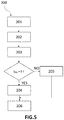
    • Figure 5 is a flow chart of a method according to the invention.
    • Figure 6 illustrates the current produced by a piezoelectric element according to the invention, the voltage across the piezoelectric element, the voltage across a storage capacitor according to the invention, and the voltage across a first switch, a second switch, a third switch and a fourth switch according to the invention over time, for the piezoelectric energy harvester according to the invention comprising a rectifier according to a first embodiment of the invention.
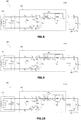
    • Figure 7 schematically represents the piezoelectric energy harvester comprising the rectifier according to the first embodiment of the invention during a second step of the method.
    • Figure 8 schematically represents the piezoelectric energy harvester comprising the rectifier according to the first embodiment of the invention during a fourth step of the method.
    • Figure 9 schematically represents the piezoelectric energy harvester comprising the rectifier according to the first embodiment of the invention during a fifth step of the method.
    • Figure 10 schematically represents the piezoelectric energy harvester comprising the rectifier according to the first embodiment of the invention during a sixth step of the method.
    DETAILED DESCRIPTION OF THE PREFERRED EMBODIMENT
  • Some embodiments of devices and methods in accordance with embodiments of the present invention are now described, by way of example only, and with reference to the accompanying drawings. The description is to be regarded as illustrative in nature and not as restrictive.
  • A first aspect of the invention relates to a rectifier for piezoelectric energy harvesting.
  • By "piezoelectric energy harvesting" is meant the collection of electrical energy produced by a piezoelectric element from mechanical energy, in order to store the electrical energy for future use.
  • By "piezoelectric element" is meant a material having the property of becoming electrically polarized under the action of a mechanical stress, and in particular under the action of a vibration, known as direct piezoelectric effect.
  • The piezoelectric element is for example a LZT material (for Lead Zirconate Titanate).
  • As illustrated in figures 1 and 2, the piezoelectric element 102 can be modeled by a dependent current source providing a current IPEH proportional to the amplitude of the vibration applied to the piezoelectric element 102, in parallel with an inherent piezoelectric capacitor CPEH.
  • The current IPEH provided by the piezoelectric element 102 and represented in figure 6 over time, is an alternative current. The alternative voltage corresponding to the current IPEH provided by the piezoelectric element 102, that is the voltage VPEH across the piezoelectric element 102, must therefore be rectified to be stored as direct voltage, which is the role of the rectifier according to the invention.
  • The rectifier 101 according to the invention represented in figures 1 and 2, comprises:
    • an active diode AD having a first terminal TAD1 and a second terminal TAD2;
    • a first switch SW0 having a first terminal T01 and a second terminal T02;
    • a second switch SW1 having a first terminal T11, a second terminal T12 and a third terminal T13;
    • a third switch SW2 having a first terminal T21, a second terminal T22 and a third terminal T23;
    • a regulator circuit REG having a first terminal TREG1 and a second terminal TREG2;
    • a fourth switch SW3 having a first terminal T31 and a second terminal T32;
    • a control circuit configured to control the position of the first switch SW0, the second switch SW1, the third switch SW2 and the fourth switch SW3, non-represented in figures 1 and 2.
  • The second switch SW1 is connected to:
    • the first terminal T01 of the first switch SW0 via its first terminal T11;
    • the ground via its second terminal T12;
    • the first terminal TAD1 of the active diode AD via its third terminal T13.
  • The third switch SW2 is connected to:
    • the second terminal T02 of the first switch SW0 via its first terminal T21;
    • the ground via its second terminal T22;
    • the first terminal TAD1 of the active diode AD via its third terminal T23.
  • The third terminal T13 of the second switch SW1 is therefore connected to the third terminal T23 of the third switch SW2 and the first switch SW0 is therefore connected to:
    • the first terminal T11 of the second switch SW1 via its first terminal T01;
    • the first terminal T21 of the third switch SW2 via its second terminal T02.
  • The first switch SW0 and the fourth switch SW3 are two-terminals switches which can be placed in an open position or in a closed position by the control circuit.
  • The second switch SW1 and the third switch SW2 are three-terminals switches which can be placed in a charging position or in a discharging position by the control circuit.
    For the second switch SW1 and the third switch SW2, in the charging position, the first terminal T11, T21 is connected to the third terminal T13, T23 and in the discharging position, the first terminal T11, T21 is connected to the second terminal T12, T22.
  • The second switch SW1 and the third switch SW2 could be each replaced by two two-terminals switches whose position would be controlled simultaneously by the control circuit.
    In this case non-represented in the figures, the second switch SW1 would be replaced by a first second switch and a second second switch each having a first terminal and a second terminal, and the third switch SW2 by a first third switch and a third second switch each having a first terminal and a second terminal, and:
    • the second terminal of the first second switch and the second terminal of the first third switch would be connected to the first terminal TAD1 of the active diode AD;
    • the first terminal of the first second switch and the first terminal of the second third switch would be connected to the first terminal T01 of the first switch SWo;
    • the first terminal of the second second switch and the first terminal of the first third switch would be connected to the second terminal T02 of the first switch SWo;
    • the second terminal of the second third switch and the second terminal of the second second switch would be connected to the ground.
  • The regulator circuit REG is connected to the second terminal TAD2 of the active diode AD via its first terminal TREG1.
  • In a first embodiment of the invention represented in figure 1, the fourth switch SW3 is connected to:
    • the first terminal TAD1 of the active diode AD via its first terminal T31;
    • the second terminal TREG2 of the regulator circuit REG via its second terminal T32.
  • In a second embodiment of the invention represented in figure 2, the rectifier 101 further comprises:
    • a recycling switch SWRCY having a first terminal TSRCY1 and a second terminal TSRCY2;
    • a recycling capacity CRCY having a first terminal TRCY1 and a second terminal TRCY2.
  • The recycling switch SWRCY is connected to:
    • the first terminal TRCY1 of the recycling capacity CRCY via its first terminal TSRCY1;
    • the second terminal TAD2 of the active diode AD via its second terminal TSRCY2.
  • The recycling capacity CRCY is connected to:
    • the first terminal TSRCY1 of the recycling switch SWRCY and to the second terminal T32 of the fourth switch SW3 via its first terminal TRCY1;
    • the ground via its second terminal TRCY2.
  • In the second embodiment, the fourth switch SW3 is connected to:
    • the third terminal T23 of the third switch SW2 via its first terminal T31;
    • the first terminal TRCY1 of the recycling capacity CRCY via its second terminal T32.
  • The recycling switch SWRCY is a two-terminals switch which can be placed in an open position or in a closed position by the regulator circuit REG.
  • One example of regulator circuit REG is represented in figure 4.
  • In figure 4, the first terminal TREG1 of the regulator circuit REG is connected to the second terminal TREG2 of the regulator circuit REG and the regulator circuit REG comprises:
    • a regulator switch SWR having a first terminal TSR1 and a second terminal TSR2;
    • a regulator comparator CompR having a non-inverting input, an inverting input and an output.
  • The regulator switch SWR is connected to:
    • the first terminal TREG1 of the regulator switch REG, that is to the second terminal TAD2 of the active diode AD, via its first terminal TSR1;
    • to the ground via its second terminal TSR2.
  • The regulator comparator CompR is connected to:
    • the second terminal TREG2 of the regulator circuit REG via its non-inverting input;
    • a reference voltage supply Vref via its inverting input.
  • The regulator switch SWR is a two-terminals switch which can be placed in an open position or in a closed position by the regulator comparator CompR.
    The regulator comparator CompR compares the voltage Vrec at the second terminal TREG2 of the regulator circuit REG and the reference voltage Vref. When the voltage Vrec at the second terminal TREG2 of the regulator circuit REG becomes superior to the reference voltage Vref, the voltage Vrcomp at the output of the regulator comparator CompR increases.
    The voltage Vrcomp at the output of the regulator comparator CompR is used to control the position of the regulator switch SWR, more specifically, the output of the regulator comparator CompR is configured to place the regulator switch SWR in the closed position when the voltage Vrec at the second terminal TREG2 of the regulator circuit REG is superior to the reference voltage Vref and to place the regulator switch SWR in the open position when the voltage Vrec at the second terminal TREG2 of the regulator circuit REG is inferior or equal to the reference voltage Vref.
  • In the second embodiment of the rectifier 101, as represented in figure 4, the voltage Vrcomp at the output of the regulator comparator CompR is also used to control the position of the recycling switch SWRCY, more specifically, the output of the regulator comparator CompR is configured to place the recycling switch SWRCY in the closed position when the voltage Vrec at the second terminal TREG2 of the regulator circuit REG is superior to the reference voltage Vref and to place the recycling switch SWRCY in the open position when the voltage Vrec at the second terminal TREG2 of the regulator circuit REG is inferior or equal to the reference voltage Vref.
  • One example of active diode AD is represented in figure 3.
  • In figure 3, the active diode AD comprises:
    • an active diode switch SWAD having a first terminal TSAD1 and a second terminal TSAD2;
    • a comparator Comp having an inverting input, a non-inverting input and an output.
  • The active diode switch SWAD is connected to the first terminal TAD1 of the active diode AD via its first terminal TSAD1 or via its second terminal TSAD2 and to the second terminal TAD2 of the active diode AD via its first terminal TSAD1 or via its second terminal TSAD2, the first terminal TSAD1 and the second terminal TSAD2 not being connected to a same terminal TAD1, TAD2 of the active diode AD.
  • The comparator Comp is connected to:
    • the first terminal TAD1 of the active diode AD via its non-inverting input;
    • the second terminal TAD2 of the active diode AD via its inverting input;
    • the control circuit CC via its output.
  • The active diode switch SWAD is a two-terminals switch which can be placed in an open position or in a closed position by the control circuit CC.
    The comparator Comp compares the voltage VSP at the first terminal TAD1 of the active diode AD and the voltage Vrec at the second terminal TAD2 of the active diode AD. When the voltage Vrec at the second terminal TAD2 of the active diode AD becomes superior to the voltage VSP at the first terminal TAD1 of the active diode AD, the voltage Vcomp at the output of the comparator Comp increases and the control circuit CC receives a higher voltage Vcomp from the comparator Comp. The control circuit CC is then configured to place the active diode switch SWAD in the open position. Otherwise, the control circuit CC is configured to place the active diode switch SWAD in the closed position.
  • The active diode switch SWAD could be a PMOS switch having a source, a drain and a gate, the first terminal TSAD1 of the active diode switch SWAD being the source, the second terminal TSAD2 of the active diode switch SWAD being the drain and the gate being connected to the control circuit CC.
  • A second aspect of the invention relates to a piezoelectric energy harvester comprising the rectifier 101 according to the first aspect of the invention.
  • As represented in figures 1 and 2, the piezoelectric energy harvester 100 further comprises:
    • the piezoelectric element 102;
    • a storage capacitor CL having a first terminal TL1 and a second terminal TL2;
    • a load resistor RL having a first terminal TR1 and a second terminal TR2.
  • The storage capacitor CL is configured to store the voltage VPEH corresponding to the current IPEH provided by the piezoelectric element 102 after rectification by the rectifier 101.
    Since CL is a storage capacitor, the value of its capacitance is at least one order of magnitude larger than the value of the capacitance of the inherent piezoelectric capacitor CPEH of the piezoelectric element 102.
  • The piezoelectric element 102 is connected in parallel with the first switch SW0, that is to the first terminal T01 of the first switch SW0 and to the second terminal T02 of the first switch SW0.
  • The storage capacitor CL is connected to:
    • the second terminal TREG2 of the regulator circuit REG via its first terminal TL1;
    • the ground via its second terminal TL2.
  • The load resistor RL is connected to:
    • the second terminal TAD2 of the regulator circuit REG via its first terminal TR1;
    • to the ground via its second terminal TR2.
  • The first terminal TL1 of the storage capacitor CL is therefore connected to the first terminal TR1 of the load resistor RL.
  • In the piezoelectric energy harvester 100, the active diode AD is used to prevent current backflow from the storage capacitor CL and to detect the zero-crossing moments of the current IPEH produced by the piezoelectric element 102.
    As previously explained, when the voltage Vrec at the first terminal TAD1 of the active diode AD, that is the voltage across the piezoelectric element 102, becomes superior to the voltage VSP at the second terminal TAD2 of the active diode AD, that is the voltage across the regulator circuit REG and therefore across the storage capacitor CL, the voltage Vcomp at the output of the comparator Comp increases. Consequently, the moment when the voltage Vcomp at the output of the comparator Comp goes high corresponds to the moment when the current IPEH produced by the piezoelectric element 102 changes direction, i.e. zero crossing.
    When the voltage Vcomp at the output of the comparator Comp goes high, the control circuit CC connected to the output of the comparator Comp places the active diode switch SWAD in the open position and prevents current backflow from the storage capacitor CL.
  • The regulator circuit REG is configured to regulate the voltage Vrec in the storage capacitor CL to prevent it from exceeding a reference voltage Vref.
    The reference voltage Vref is for example equal to the maximum no-load voltage across the piezoelectric element 102 obtained when a vibration is applied to the piezoelectric element 102 when it is not connected to the rectifier 101.
    As previously explained, when the voltage Vrec at the second terminal TSAD2 of the regulator circuit REG, that is the voltage at the first terminal TL1 of the storage capacitor CL becomes superior to the reference voltage Vref, the voltage Vrcomp at the output of the regulator comparator CompR increases, which is used to place the regulator switch SWR in the closed position, and to place the recycling switch SWRCY in the closed position in the second embodiment of the rectifier 101. Consequently, in the second embodiment of the rectifier 101, when the voltage Vrec at the first terminal TL1 of the storage capacitor CL becomes superior to the reference voltage Vref, the regulator switch SWR and the recycling switch SWRCY are placed in the closed position by the regulator comparator CompR via the voltage Vrcomp at its output and the voltage Vrec across the storage capacitor CL in excess is stored in the recycling capacitor CRCY.
  • A third aspect of the invention relates to a method for harvesting piezoelectric energy using the piezoelectric energy harvester 100 according to the second aspect of the invention.
  • The sequence of the steps of the method 200 according to the invention is represented in figure 5.
  • A first step 201 of the method 200 consists in detecting the zero-crossing moments of the current IPEH produced by the piezoelectric element 102.
    The first step 201 is realized by the active diode AD if the rectifier 101 comprises an active diode AD according to the example represented in figure 3.
  • The following steps of the method 200 are realized at each zero-crossing moment detected at the first step 201.
  • A second step 202 of the method 200 consists in:
    • putting the second switch SW1 and/or the third switch SW2 in the discharging position via the control circuit CC, in such a way that the second switch SW1 and the third switch SW2 are both in the discharging position;
    • closing the first switch SW0 via the control circuit CC.
  • At the end of the second step 202, the second switch SW1 and the third switch SW2 are in the discharging position and the first switch SW0 is closed, which creates a short-circuit of the piezoelectric element 102 and forces the inherent piezoelectric capacitor CPEH to discharge.
  • In figure 6, one can see that the absolute value of the voltage VPEH across the piezoelectric element 102 decreases to zero as soon as the first switch SW0 is closed, that is as soon as the voltage across the first switch SW0 is non-zero.
  • In figure 7 is represented the piezoelectric energy harvester 100 comprising a rectifier 101 according to the first embodiment, at the end of the second step 202.
  • A third step 203 of the method 200 is realized after a discharging time td.
    The discharging time td is for example in the range of a few tens of nanoseconds to 1 microsecond.
  • The third step 203 consists in:
    • opening the first switch SWo;
    • closing the fourth switch SW3;
    • checking the sign of the current IPEH produced by the piezoelectric element 102.
  • If the current IPEH produced by the piezoelectric element 102 is positive, a fourth step 204 is realized.
    If the current IPEH produced by the piezoelectric element 102 is negative, a fifth step 205 is realized.
  • The fourth step 204 consists in putting the second switch SW1 in the charging position.
  • In figure 8 is represented the piezoelectric energy harvester 100 comprising a rectifier 101 according to the first embodiment, at the end of the fourth step 204.
  • The fifth step 205 consists in putting the third switch SW2 in the charging position.
  • In figure 9 is represented the piezoelectric energy harvester 100 comprising a rectifier 101 according to the first embodiment, at the end of the fifth step 205.
  • At the end of the fourth step 204 if the current IPEH is positive or of the fifth step 205 if the current IPEH is negative, the inherent piezoelectric capacitor CPEH is in parallel with the storage capacitor CL and the active diode AD is short-circuited, which allows charges from the storage capacitor CL to be transferred to the inherent piezoelectric capacitor CPEH.
    In figure 6, one can see that the voltage VPEH across the piezoelectric element 102 increases to reach a value +/- Vm as soon as the fourth switch SW3 is closed, that is as soon as the voltage across the fourth switch SW3 is non-zero, and that the voltage Vrect across the storage capacitor CL decreases from a maximum value +VM to a value +Vm.
  • At the end of the fourth step 204, if the current IPEH is positive or of the fifth step 205 if the current IPEH is negative for the piezoelectric energy harvester 100 comprising a rectifier 101 according to the second embodiment, the inherent piezoelectric capacitor CPEH is in parallel with the recycling capacitor CRCY and the active diode AD is short-circuited, which allows charges from the recycling capacitor CRCY to be transferred to the inherent piezoelectric capacitor CPEH.
  • A sixth step 206 of the method 200 is realized after a recharging time tr.
    The recharging time tr is for example in the range of a few hundred nanoseconds to 1 microsecond.
  • The sixth step 206 consists in opening the fourth switch SW3.
  • In figure 10 is represented the piezoelectric energy harvester 100 comprising a rectifier 101 according to the first embodiment, at the end of the sixth step 206 if the current IPEH produced by the piezoelectric element 102 was positive at the third step 203.
  • At the end of the sixth step 206, the inherent piezoelectric capacitor CPEH is in parallel with the storage capacitor CL but the active diode AD is not short-circuited anymore.
    For the active diode AD represented in figure 3, the active diode switch SWAD of the active diode AD is placed in the closed position as soon as the voltage VPEH across the piezoelectric element 102 is higher than the voltage Vrect across the storage capacitor CL. As a result, most of the charges delivered by the piezoelectric element 102 are transferred to the storage capacitor CL and to the load resistor RL.
  • In figure 6, one can see that the absolute value of the voltage VPEH across the piezoelectric element 102 increases gradually from +/- Vm to +/- VM as soon as the fourth switch SW3 is opened, that is as soon as the voltage across the fourth switch SW3 is equal to zero, and the voltage Vrect across the storage capacitor CL also increases gradually from +Vm to +VM.

Claims (7)

  1. Rectifier (101) for piezoelectric energy harvesting, characterized in that it comprises:
    - an active diode (AD) having a first terminal (TAD1) and a second terminal (TAD2);
    - a first switch (SW0) having a first terminal (T01) and a second terminal (T02);
    - a second switch (SW1) having a first terminal (T11), a second terminal (T12) and a third terminal (T13), the first terminal (T11) of the second switch (SW1) being connected to the first terminal (T01) of the first switch (SWo), the second terminal (T12) of the second switch (SW1) being connected to the ground and the third terminal (T13) of the second switch (SW1) being connected to the first terminal (TAD1) of the active diode (AD), the first terminal (T11) of the second switch (SW1) being connected to the third terminal (T13) of the second switch (SW1) in a charging position and the first terminal (T11) of the second switch (SW1) being connected to the second terminal (T12) of the second switch (SW1) in a discharging position;
    - a third switch (SW2) having a first terminal (T21), a second terminal (T22) and a third terminal (T23), the first terminal (T21) of the third switch (SW2) being connected to the second terminal (T02) of the first switch (SWo), the second terminal (T22) of the third switch (SW2) being connected to the ground and the third terminal (T23) of the third switch (SW2) being connected to the first terminal (TAD1) of the active diode (AD), the first terminal (T21) of the third switch (SW2) being connected to the third terminal (T23) of the third switch (SW2) in a charging position and the first terminal (T21) of the third switch (SW2) being connected to the second terminal (T22) of the third switch (SW2) in a discharging position;
    - a regulator circuit (REG) having a first terminal (TREG1) and a second terminal (TREG2), the first terminal (TREG1) of the regulator circuit (REG) being connected to the second terminal (TAD2) of the active diode (AD);
    - either a fourth switch (SW3) having a first terminal (T31) and a second terminal (T32), the first terminal (T31) of the fourth switch (SW3) being connected to the first terminal (TA1) of the active diode (AD) and the second terminal (T32) of the fourth switch (SW3) being connected to the second terminal (TREG2) of the regulator circuit (REG);
    - or:
    ∘ a recycling switch (SWRCY) having a first terminal (TSRCY1) and a second terminal (TSRCY2), the second terminal (TSRCY2) of the recycling switch (SWRCY) being connected to the second terminal (TAD2) of the active diode (AD);
    ∘ a recycling capacity (CRCY) having a first terminal (TRCY1) and a second terminal (TRCY2), the first terminal (TRCY1) of the recycling capacity (CRCY) being connected to the first terminal (TSRCY1) of the recycling switch (SWRCY) and the second terminal (TRCY2) of the recycling capacity (CRCY) being connected to the ground; and
    ∘ a fourth switch (SW3) having a first terminal (T31) and a second terminal (T32), the first terminal (T31) of the fourth switch (SW3) being connected to the third terminal (T23) of the third switch (SW2) and the second terminal (T32) of the fourth switch (SW3) being connected to the first terminal (TRCY1) of the recycling capacity (CRCY);
    - a control circuit (CC) configured to control the position of the first switch (SWo), the second switch (SW1), the third switch (SW2) and the fourth switch (SW3).
  2. Rectifier (101) according to claim 1, characterized in that the active diode (AD) comprises:
    - an active diode switch (SWAD) having a first terminal (TSAD1) and a second terminal (TSAD2) being each connected to one different terminal (TAD1, TAD2) of the active diode (AD);
    - a comparator (Comp) having:
    ∘ an inverting input connected to the second terminal (TAD2) of the active diode (AD);
    ∘ a non-inverting input connected to the first terminal (TAD1) of the active diode (AD); and
    ∘ an output connected to the control circuit (CC);
    the control circuit (CC) being configured to open the active diode switch (SWAD) when the voltage (VSP) at the non-inverting input of the comparator (Comp) is superior to the voltage (Vrec) at the inverting input of the comparator (Comp) and to close the active diode switch (SWAD) when the voltage (VSP) at the non-inverting input of the comparator (Comp) is inferior or equal to the voltage (Vrec) at the inverting input of the comparator (Comp).
  3. Rectifier (101) according to any of the preceding claims, characterized in that the first terminal (TREG1) of the regulator circuit (REG) is connected to the second terminal (TREG2) of the regulator circuit (REG) and the regulator circuit (REG) comprises:
    - a regulator switch (SWR) having a first terminal (TSR1) and a second terminal (TSR2), the first terminal (TSR1) of the regulator switch (SWR) being connected to the first terminal (TREG1) of the regulator circuit (REG) and the second terminal (TSR2) of the regulator switch (SWR) being connected to the ground;
    - a regulator comparator (CompR) having:
    ∘ a non-inverting input connected to the second terminal (TREG2) of the regulator circuit (REG);
    ∘ an inverting input connected to a reference voltage (Vref) supply; and
    ∘ an output configured to close the regulator switch (SWR) when the voltage (Vrec) at the non-inverting input of the regulator comparator (CompR) is superior to the voltage (Vref) at the inverting input of the regulator comparator (CompR) and to open the regulator switch (SWR) when the voltage (Vrec) at the non-inverting input of the regulator comparator (CompR) is inferior or equal to the voltage (Vref) at the inverting input of the regulator comparator (CompR).
  4. Rectifier (101) according to claim 3, characterized in that the output of the regulator comparator (CompR) is configured to close the recycling switch (SWRCY) when the voltage (Vrec) at the non-inverting input of the regulator comparator (CompR) is superior to the voltage (Vref) at the inverting input of the regulator comparator (CompR) and to open the recycling switch (SWRCY) when the voltage (Vrec) at the non-inverting input of the regulator comparator (CompR) is inferior or equal to the voltage (Vref) at the inverting input of the comparator (CompR).
  5. Piezoelectric energy harvester (100) comprising:
    - a piezoelectric element (102) configured to convert mechanical energy into electrical energy in the form of an alternating current (IPEH) corresponding to an alternating voltage (VPEH);
    - a rectifier (101) according to any of the preceding claims, configured to rectify the alternating voltage (VPEH), the piezoelectric element (102) being connected in parallel with the first switch (SWo);
    - a storage capacitor (CL) configured to store the rectified voltage, having a first terminal (TL1) and a second terminal (TL2), the first terminal (TL1) of the storage capacitor (CL) being connected to the second terminal (TREG2) of the regulator circuit (REG) and the second terminal (TL2) of the storage capacitor (CL) being connected to the ground, the regulator circuit (REG) being configured to regulate the voltage (Vrec) in the storage capacitor (CL);
    - a load resistor (RL), having a first terminal (TR1) and a second terminal (TR2), the first terminal (TR1) of the load resistor (RL) being connected to the second terminal (TREG2) of the regulator circuit (REG) and the second terminal (TR2) of the load resistor (RL) being connected to the ground.
  6. Piezoelectric energy harvester (100) according to claim 5 comprising a rectifier (101) according to claim 3 or 4, characterized in that the reference voltage (Vref) is equal to a maximum no-load voltage across the piezoelectric element (102).
  7. Method (200) for harvesting piezoelectric energy using the piezoelectric energy harvester (100) according to any of claim 5 or 6, comprising the following steps:
    - Detect the zero-crossing moments of the current (IPEH) produced by the piezoelectric element (102, 201);
    - When a zero-crossing moment is detected:
    ∘ Via the control circuit (CC), put the second switch (SW1) and/or the third switch (SW2) in the discharging position, and close the first switch (SWo, 202);
    ∘ At the end of a discharging time (td), open the first switch (SW0) and close the fourth switch (SW3) via the control circuit (CC), and check the sign of the current (IPEH) produced by the piezoelectric element (102, 203):
    ▪ If the current (IPEH) produced by the piezoelectric element (102) is positive, put the second switch (SW1) in the charging position via the control circuit (CC, 204);
    ▪ If the current (IPEH) produced by the piezoelectric element (102) is negative, put the third switch (SW2) in the charging position via the control circuit (CC, 205);
    ∘ At the end of the recharging time (tr), open the fourth switch (SW3) via the control circuit (CC, 206).
EP20178812.2A 2020-06-08 2020-06-08 Rectifier for piezoelectric energy harvesting, piezoelectric energy harvester and associated method Withdrawn EP3923459A1 (en)

Priority Applications (2)

Application Number Priority Date Filing Date Title
EP20178812.2A EP3923459A1 (en) 2020-06-08 2020-06-08 Rectifier for piezoelectric energy harvesting, piezoelectric energy harvester and associated method
PCT/EP2021/065130 WO2021249919A1 (en) 2020-06-08 2021-06-07 Rectifier for piezoelectric energy harvesting, piezoelectric energy harvester and associated method

Applications Claiming Priority (1)

Application Number Priority Date Filing Date Title
EP20178812.2A EP3923459A1 (en) 2020-06-08 2020-06-08 Rectifier for piezoelectric energy harvesting, piezoelectric energy harvester and associated method

Publications (1)

Publication Number Publication Date
EP3923459A1 true EP3923459A1 (en) 2021-12-15

Family

ID=71078414

Family Applications (1)

Application Number Title Priority Date Filing Date
EP20178812.2A Withdrawn EP3923459A1 (en) 2020-06-08 2020-06-08 Rectifier for piezoelectric energy harvesting, piezoelectric energy harvester and associated method

Country Status (2)

Country Link
EP (1) EP3923459A1 (en)
WO (1) WO2021249919A1 (en)

Family Cites Families (1)

* Cited by examiner, † Cited by third party
Publication number Priority date Publication date Assignee Title
CN112771775B (en) * 2018-09-28 2023-12-01 三菱电机株式会社 Power conversion devices, motor drive devices and air conditioners

Non-Patent Citations (2)

* Cited by examiner, † Cited by third party
Title
NIELSEN-LONN MARTIN ET AL: "Design considerations for interface circuits to low-voltage piezoelectric energy harvesters", 2014 NORCHIP, IEEE, 27 October 2014 (2014-10-27), pages 1 - 4, XP032715650, DOI: 10.1109/NORCHIP.2014.7004722 *
SHANG YU ET AL: "A Miniature and High-efficiency Interface Circuit Based on SSHC for Piezoelectric Energy Harvesting", 2019 IEEE INTERNATIONAL CONFERENCE ON ELECTRON DEVICES AND SOLID-STATE CIRCUITS (EDSSC), IEEE, 12 June 2019 (2019-06-12), pages 1 - 3, XP033573074, DOI: 10.1109/EDSSC.2019.8754463 *

Also Published As

Publication number Publication date
WO2021249919A1 (en) 2021-12-16

Similar Documents

Publication Publication Date Title
US7049711B2 (en) Uninterruptible power system
US9941722B2 (en) Converter and method for extracting maximum power from piezo vibration harvester
US9800170B2 (en) Energy harvester open-circuit voltage sensing for MPPT
CN109905042A (en) A power supply device and its power supply circuit
US20110199057A1 (en) Battery protection circuit and method for energy harvester circuit
EP2302757A1 (en) Method and system for balancing electrical energy storage cells
US20090015211A1 (en) Method and related device for charging at the same voltage two or more capacitors connected in series
WO2009036115A1 (en) Method and apparatus for providing power
EP3642930A1 (en) System and method for supercapacitor charging and balancing
US9160223B2 (en) Rectifier circuit, and environmental energy harvesting system comprising the rectifier circuit
JP2010041910A (en) Power supply apparatus
Çiftci et al. Low-cost fully autonomous piezoelectric energy harvesting interface circuit with up to 6.14 x power capacity gain
US20110255314A1 (en) Switched power converter with extended hold-up time
JPH1014127A (en) Multifunctional battery charger self-aligns as a supply voltage regulator for battery powered devices
KR101319284B1 (en) Dc-dc converter and power supply device
JP6274289B1 (en) Power circuit
EP3923459A1 (en) Rectifier for piezoelectric energy harvesting, piezoelectric energy harvester and associated method
US6285567B1 (en) Methods and apparatus for utilizing the transformer leakage energy in a power supply
WO2013132441A2 (en) Low load, low frequency piezo-electric power generator
JP2010172111A (en) Regulator circuit
US11509219B2 (en) Reservoir capacitor for boost converters
KR20240000708A (en) Highly efficient transformer circuit device combining inductor-based pressure reducer and series-parallel conversion capacitor for kinetic energy harvester and method of operation thereof
US5923155A (en) Circuit for the production of an auxiliary voltage
JPH02155470A (en) Switching circuit
CN223039909U (en) Switching power supply boost circuit

Legal Events

Date Code Title Description
PUAI Public reference made under article 153(3) epc to a published international application that has entered the european phase

Free format text: ORIGINAL CODE: 0009012

STAA Information on the status of an ep patent application or granted ep patent

Free format text: STATUS: THE APPLICATION HAS BEEN PUBLISHED

AK Designated contracting states

Kind code of ref document: A1

Designated state(s): AL AT BE BG CH CY CZ DE DK EE ES FI FR GB GR HR HU IE IS IT LI LT LU LV MC MK MT NL NO PL PT RO RS SE SI SK SM TR

B565 Issuance of search results under rule 164(2) epc

Effective date: 20201119

STAA Information on the status of an ep patent application or granted ep patent

Free format text: STATUS: THE APPLICATION IS DEEMED TO BE WITHDRAWN

18D Application deemed to be withdrawn

Effective date: 20220616