EP3923307B1 - Magnetic integrated device, power conversion circuit, charger, and electric vehicle - Google Patents
Magnetic integrated device, power conversion circuit, charger, and electric vehicle Download PDFInfo
- Publication number
- EP3923307B1 EP3923307B1 EP20852993.3A EP20852993A EP3923307B1 EP 3923307 B1 EP3923307 B1 EP 3923307B1 EP 20852993 A EP20852993 A EP 20852993A EP 3923307 B1 EP3923307 B1 EP 3923307B1
- Authority
- EP
- European Patent Office
- Prior art keywords
- transformer winding
- magnetic
- integrated device
- winding
- transformer
- Prior art date
- Legal status (The legal status is an assumption and is not a legal conclusion. Google has not performed a legal analysis and makes no representation as to the accuracy of the status listed.)
- Active
Links
Images




Classifications
-
- H—ELECTRICITY
- H02—GENERATION; CONVERSION OR DISTRIBUTION OF ELECTRIC POWER
- H02M—APPARATUS FOR CONVERSION BETWEEN AC AND AC, BETWEEN AC AND DC, OR BETWEEN DC AND DC, AND FOR USE WITH MAINS OR SIMILAR POWER SUPPLY SYSTEMS; CONVERSION OF DC OR AC INPUT POWER INTO SURGE OUTPUT POWER; CONTROL OR REGULATION THEREOF
- H02M3/00—Conversion of DC power input into DC power output
- H02M3/22—Conversion of DC power input into DC power output with intermediate conversion into AC
- H02M3/24—Conversion of DC power input into DC power output with intermediate conversion into AC by static converters
- H02M3/28—Conversion of DC power input into DC power output with intermediate conversion into AC by static converters using discharge tubes with control electrode or semiconductor devices with control electrode to produce the intermediate AC
- H02M3/325—Conversion of DC power input into DC power output with intermediate conversion into AC by static converters using discharge tubes with control electrode or semiconductor devices with control electrode to produce the intermediate AC using devices of a triode or a transistor type requiring continuous application of a control signal
- H02M3/335—Conversion of DC power input into DC power output with intermediate conversion into AC by static converters using discharge tubes with control electrode or semiconductor devices with control electrode to produce the intermediate AC using devices of a triode or a transistor type requiring continuous application of a control signal using semiconductor devices only
- H02M3/33569—Conversion of DC power input into DC power output with intermediate conversion into AC by static converters using discharge tubes with control electrode or semiconductor devices with control electrode to produce the intermediate AC using devices of a triode or a transistor type requiring continuous application of a control signal using semiconductor devices only having several active switching elements
- H02M3/33573—Full-bridge at primary side of an isolation transformer
-
- H—ELECTRICITY
- H01—ELECTRIC ELEMENTS
- H01F—MAGNETS; INDUCTANCES; TRANSFORMERS; SELECTION OF MATERIALS FOR THEIR MAGNETIC PROPERTIES
- H01F27/00—Details of transformers or inductances, in general
- H01F27/34—Special means for preventing or reducing unwanted electric or magnetic effects, e.g. no-load losses, reactive currents, harmonics, oscillations, leakage fields
- H01F27/38—Auxiliary core members; Auxiliary coils or windings
-
- B—PERFORMING OPERATIONS; TRANSPORTING
- B60—VEHICLES IN GENERAL
- B60L—PROPULSION OF ELECTRICALLY-PROPELLED VEHICLES; SUPPLYING ELECTRIC POWER FOR AUXILIARY EQUIPMENT OF ELECTRICALLY-PROPELLED VEHICLES; ELECTRODYNAMIC BRAKE SYSTEMS FOR VEHICLES IN GENERAL; MAGNETIC SUSPENSION OR LEVITATION FOR VEHICLES; MONITORING OPERATING VARIABLES OF ELECTRICALLY-PROPELLED VEHICLES; ELECTRIC SAFETY DEVICES FOR ELECTRICALLY-PROPELLED VEHICLES
- B60L53/00—Methods of charging batteries, specially adapted for electric vehicles; Charging stations or on-board charging equipment therefor; Exchange of energy storage elements in electric vehicles
- B60L53/20—Methods of charging batteries, specially adapted for electric vehicles; Charging stations or on-board charging equipment therefor; Exchange of energy storage elements in electric vehicles characterised by converters located in the vehicle
- B60L53/22—Constructional details or arrangements of charging converters specially adapted for charging electric vehicles
-
- H—ELECTRICITY
- H01—ELECTRIC ELEMENTS
- H01F—MAGNETS; INDUCTANCES; TRANSFORMERS; SELECTION OF MATERIALS FOR THEIR MAGNETIC PROPERTIES
- H01F27/00—Details of transformers or inductances, in general
- H01F27/24—Magnetic cores
-
- H—ELECTRICITY
- H01—ELECTRIC ELEMENTS
- H01F—MAGNETS; INDUCTANCES; TRANSFORMERS; SELECTION OF MATERIALS FOR THEIR MAGNETIC PROPERTIES
- H01F27/00—Details of transformers or inductances, in general
- H01F27/28—Coils; Windings; Conductive connections
-
- H—ELECTRICITY
- H01—ELECTRIC ELEMENTS
- H01F—MAGNETS; INDUCTANCES; TRANSFORMERS; SELECTION OF MATERIALS FOR THEIR MAGNETIC PROPERTIES
- H01F27/00—Details of transformers or inductances, in general
- H01F27/28—Coils; Windings; Conductive connections
- H01F27/2804—Printed windings
-
- H—ELECTRICITY
- H01—ELECTRIC ELEMENTS
- H01F—MAGNETS; INDUCTANCES; TRANSFORMERS; SELECTION OF MATERIALS FOR THEIR MAGNETIC PROPERTIES
- H01F27/00—Details of transformers or inductances, in general
- H01F27/28—Coils; Windings; Conductive connections
- H01F27/2823—Wires
-
- H—ELECTRICITY
- H01—ELECTRIC ELEMENTS
- H01F—MAGNETS; INDUCTANCES; TRANSFORMERS; SELECTION OF MATERIALS FOR THEIR MAGNETIC PROPERTIES
- H01F27/00—Details of transformers or inductances, in general
- H01F27/28—Coils; Windings; Conductive connections
- H01F27/2871—Pancake coils
-
- H—ELECTRICITY
- H01—ELECTRIC ELEMENTS
- H01F—MAGNETS; INDUCTANCES; TRANSFORMERS; SELECTION OF MATERIALS FOR THEIR MAGNETIC PROPERTIES
- H01F27/00—Details of transformers or inductances, in general
- H01F27/28—Coils; Windings; Conductive connections
- H01F27/30—Fastening or clamping coils, windings, or parts thereof together; Fastening or mounting coils or windings on core, casing, or other support
- H01F27/306—Fastening or mounting coils or windings on core, casing or other support
-
- H—ELECTRICITY
- H01—ELECTRIC ELEMENTS
- H01F—MAGNETS; INDUCTANCES; TRANSFORMERS; SELECTION OF MATERIALS FOR THEIR MAGNETIC PROPERTIES
- H01F27/00—Details of transformers or inductances, in general
- H01F27/34—Special means for preventing or reducing unwanted electric or magnetic effects, e.g. no-load losses, reactive currents, harmonics, oscillations, leakage fields
- H01F27/346—Preventing or reducing leakage fields
-
- H—ELECTRICITY
- H01—ELECTRIC ELEMENTS
- H01F—MAGNETS; INDUCTANCES; TRANSFORMERS; SELECTION OF MATERIALS FOR THEIR MAGNETIC PROPERTIES
- H01F27/00—Details of transformers or inductances, in general
- H01F27/40—Structural association with built-in electric component, e.g. fuse
-
- H—ELECTRICITY
- H01—ELECTRIC ELEMENTS
- H01F—MAGNETS; INDUCTANCES; TRANSFORMERS; SELECTION OF MATERIALS FOR THEIR MAGNETIC PROPERTIES
- H01F3/00—Cores, Yokes, or armatures
- H01F3/10—Composite arrangements of magnetic circuits
- H01F3/14—Constrictions; Gaps, e.g. air-gaps
-
- H—ELECTRICITY
- H01—ELECTRIC ELEMENTS
- H01F—MAGNETS; INDUCTANCES; TRANSFORMERS; SELECTION OF MATERIALS FOR THEIR MAGNETIC PROPERTIES
- H01F38/00—Adaptations of transformers or inductances for specific applications or functions
-
- H—ELECTRICITY
- H02—GENERATION; CONVERSION OR DISTRIBUTION OF ELECTRIC POWER
- H02M—APPARATUS FOR CONVERSION BETWEEN AC AND AC, BETWEEN AC AND DC, OR BETWEEN DC AND DC, AND FOR USE WITH MAINS OR SIMILAR POWER SUPPLY SYSTEMS; CONVERSION OF DC OR AC INPUT POWER INTO SURGE OUTPUT POWER; CONTROL OR REGULATION THEREOF
- H02M1/00—Details of apparatus for conversion
- H02M1/0067—Converter structures employing plural converter units, other than for parallel operation of the units on a single load
- H02M1/0074—Plural converter units whose inputs are connected in series
-
- H—ELECTRICITY
- H02—GENERATION; CONVERSION OR DISTRIBUTION OF ELECTRIC POWER
- H02M—APPARATUS FOR CONVERSION BETWEEN AC AND AC, BETWEEN AC AND DC, OR BETWEEN DC AND DC, AND FOR USE WITH MAINS OR SIMILAR POWER SUPPLY SYSTEMS; CONVERSION OF DC OR AC INPUT POWER INTO SURGE OUTPUT POWER; CONTROL OR REGULATION THEREOF
- H02M1/00—Details of apparatus for conversion
- H02M1/0067—Converter structures employing plural converter units, other than for parallel operation of the units on a single load
- H02M1/008—Plural converter units for generating at two or more independent and non-parallel outputs, e.g. systems with plural point of load switching regulators
-
- H—ELECTRICITY
- H02—GENERATION; CONVERSION OR DISTRIBUTION OF ELECTRIC POWER
- H02M—APPARATUS FOR CONVERSION BETWEEN AC AND AC, BETWEEN AC AND DC, OR BETWEEN DC AND DC, AND FOR USE WITH MAINS OR SIMILAR POWER SUPPLY SYSTEMS; CONVERSION OF DC OR AC INPUT POWER INTO SURGE OUTPUT POWER; CONTROL OR REGULATION THEREOF
- H02M3/00—Conversion of DC power input into DC power output
- H02M3/01—Resonant DC/DC converters
-
- H—ELECTRICITY
- H02—GENERATION; CONVERSION OR DISTRIBUTION OF ELECTRIC POWER
- H02M—APPARATUS FOR CONVERSION BETWEEN AC AND AC, BETWEEN AC AND DC, OR BETWEEN DC AND DC, AND FOR USE WITH MAINS OR SIMILAR POWER SUPPLY SYSTEMS; CONVERSION OF DC OR AC INPUT POWER INTO SURGE OUTPUT POWER; CONTROL OR REGULATION THEREOF
- H02M3/00—Conversion of DC power input into DC power output
- H02M3/22—Conversion of DC power input into DC power output with intermediate conversion into AC
- H02M3/24—Conversion of DC power input into DC power output with intermediate conversion into AC by static converters
- H02M3/28—Conversion of DC power input into DC power output with intermediate conversion into AC by static converters using discharge tubes with control electrode or semiconductor devices with control electrode to produce the intermediate AC
-
- H—ELECTRICITY
- H02—GENERATION; CONVERSION OR DISTRIBUTION OF ELECTRIC POWER
- H02M—APPARATUS FOR CONVERSION BETWEEN AC AND AC, BETWEEN AC AND DC, OR BETWEEN DC AND DC, AND FOR USE WITH MAINS OR SIMILAR POWER SUPPLY SYSTEMS; CONVERSION OF DC OR AC INPUT POWER INTO SURGE OUTPUT POWER; CONTROL OR REGULATION THEREOF
- H02M3/00—Conversion of DC power input into DC power output
- H02M3/22—Conversion of DC power input into DC power output with intermediate conversion into AC
- H02M3/24—Conversion of DC power input into DC power output with intermediate conversion into AC by static converters
- H02M3/28—Conversion of DC power input into DC power output with intermediate conversion into AC by static converters using discharge tubes with control electrode or semiconductor devices with control electrode to produce the intermediate AC
- H02M3/325—Conversion of DC power input into DC power output with intermediate conversion into AC by static converters using discharge tubes with control electrode or semiconductor devices with control electrode to produce the intermediate AC using devices of a triode or a transistor type requiring continuous application of a control signal
- H02M3/335—Conversion of DC power input into DC power output with intermediate conversion into AC by static converters using discharge tubes with control electrode or semiconductor devices with control electrode to produce the intermediate AC using devices of a triode or a transistor type requiring continuous application of a control signal using semiconductor devices only
- H02M3/33569—Conversion of DC power input into DC power output with intermediate conversion into AC by static converters using discharge tubes with control electrode or semiconductor devices with control electrode to produce the intermediate AC using devices of a triode or a transistor type requiring continuous application of a control signal using semiconductor devices only having several active switching elements
- H02M3/33576—Conversion of DC power input into DC power output with intermediate conversion into AC by static converters using discharge tubes with control electrode or semiconductor devices with control electrode to produce the intermediate AC using devices of a triode or a transistor type requiring continuous application of a control signal using semiconductor devices only having several active switching elements having at least one active switching element at the secondary side of an isolation transformer
-
- H—ELECTRICITY
- H02—GENERATION; CONVERSION OR DISTRIBUTION OF ELECTRIC POWER
- H02M—APPARATUS FOR CONVERSION BETWEEN AC AND AC, BETWEEN AC AND DC, OR BETWEEN DC AND DC, AND FOR USE WITH MAINS OR SIMILAR POWER SUPPLY SYSTEMS; CONVERSION OF DC OR AC INPUT POWER INTO SURGE OUTPUT POWER; CONTROL OR REGULATION THEREOF
- H02M3/00—Conversion of DC power input into DC power output
- H02M3/22—Conversion of DC power input into DC power output with intermediate conversion into AC
- H02M3/24—Conversion of DC power input into DC power output with intermediate conversion into AC by static converters
- H02M3/28—Conversion of DC power input into DC power output with intermediate conversion into AC by static converters using discharge tubes with control electrode or semiconductor devices with control electrode to produce the intermediate AC
- H02M3/325—Conversion of DC power input into DC power output with intermediate conversion into AC by static converters using discharge tubes with control electrode or semiconductor devices with control electrode to produce the intermediate AC using devices of a triode or a transistor type requiring continuous application of a control signal
- H02M3/335—Conversion of DC power input into DC power output with intermediate conversion into AC by static converters using discharge tubes with control electrode or semiconductor devices with control electrode to produce the intermediate AC using devices of a triode or a transistor type requiring continuous application of a control signal using semiconductor devices only
- H02M3/33569—Conversion of DC power input into DC power output with intermediate conversion into AC by static converters using discharge tubes with control electrode or semiconductor devices with control electrode to produce the intermediate AC using devices of a triode or a transistor type requiring continuous application of a control signal using semiconductor devices only having several active switching elements
- H02M3/33576—Conversion of DC power input into DC power output with intermediate conversion into AC by static converters using discharge tubes with control electrode or semiconductor devices with control electrode to produce the intermediate AC using devices of a triode or a transistor type requiring continuous application of a control signal using semiconductor devices only having several active switching elements having at least one active switching element at the secondary side of an isolation transformer
- H02M3/33584—Bidirectional converters
-
- H—ELECTRICITY
- H02—GENERATION; CONVERSION OR DISTRIBUTION OF ELECTRIC POWER
- H02M—APPARATUS FOR CONVERSION BETWEEN AC AND AC, BETWEEN AC AND DC, OR BETWEEN DC AND DC, AND FOR USE WITH MAINS OR SIMILAR POWER SUPPLY SYSTEMS; CONVERSION OF DC OR AC INPUT POWER INTO SURGE OUTPUT POWER; CONTROL OR REGULATION THEREOF
- H02M3/00—Conversion of DC power input into DC power output
- H02M3/22—Conversion of DC power input into DC power output with intermediate conversion into AC
- H02M3/24—Conversion of DC power input into DC power output with intermediate conversion into AC by static converters
- H02M3/28—Conversion of DC power input into DC power output with intermediate conversion into AC by static converters using discharge tubes with control electrode or semiconductor devices with control electrode to produce the intermediate AC
- H02M3/285—Single converters with a plurality of output stages connected in parallel
-
- Y—GENERAL TAGGING OF NEW TECHNOLOGICAL DEVELOPMENTS; GENERAL TAGGING OF CROSS-SECTIONAL TECHNOLOGIES SPANNING OVER SEVERAL SECTIONS OF THE IPC; TECHNICAL SUBJECTS COVERED BY FORMER USPC CROSS-REFERENCE ART COLLECTIONS [XRACs] AND DIGESTS
- Y02—TECHNOLOGIES OR APPLICATIONS FOR MITIGATION OR ADAPTATION AGAINST CLIMATE CHANGE
- Y02T—CLIMATE CHANGE MITIGATION TECHNOLOGIES RELATED TO TRANSPORTATION
- Y02T10/00—Road transport of goods or passengers
- Y02T10/60—Other road transportation technologies with climate change mitigation effect
- Y02T10/70—Energy storage systems for electromobility, e.g. batteries
-
- Y—GENERAL TAGGING OF NEW TECHNOLOGICAL DEVELOPMENTS; GENERAL TAGGING OF CROSS-SECTIONAL TECHNOLOGIES SPANNING OVER SEVERAL SECTIONS OF THE IPC; TECHNICAL SUBJECTS COVERED BY FORMER USPC CROSS-REFERENCE ART COLLECTIONS [XRACs] AND DIGESTS
- Y02—TECHNOLOGIES OR APPLICATIONS FOR MITIGATION OR ADAPTATION AGAINST CLIMATE CHANGE
- Y02T—CLIMATE CHANGE MITIGATION TECHNOLOGIES RELATED TO TRANSPORTATION
- Y02T10/00—Road transport of goods or passengers
- Y02T10/60—Other road transportation technologies with climate change mitigation effect
- Y02T10/7072—Electromobility specific charging systems or methods for batteries, ultracapacitors, supercapacitors or double-layer capacitors
-
- Y—GENERAL TAGGING OF NEW TECHNOLOGICAL DEVELOPMENTS; GENERAL TAGGING OF CROSS-SECTIONAL TECHNOLOGIES SPANNING OVER SEVERAL SECTIONS OF THE IPC; TECHNICAL SUBJECTS COVERED BY FORMER USPC CROSS-REFERENCE ART COLLECTIONS [XRACs] AND DIGESTS
- Y02—TECHNOLOGIES OR APPLICATIONS FOR MITIGATION OR ADAPTATION AGAINST CLIMATE CHANGE
- Y02T—CLIMATE CHANGE MITIGATION TECHNOLOGIES RELATED TO TRANSPORTATION
- Y02T90/00—Enabling technologies or technologies with a potential or indirect contribution to GHG emissions mitigation
- Y02T90/10—Technologies relating to charging of electric vehicles
- Y02T90/14—Plug-in electric vehicles
Definitions
- a resonant converter comprises a resonant circuit, wherein the resonant circuit comprises a first resonant capacitor, an integrated magnetic component and a second resonant capacitor, an integrated magnetic component and a second resonant capacitor, a first winding comprises a first winding part and a second winding part, a second winding comprises a third winding part and a fourth winding part, the first winding part is wound around a first magnetic post and a fourth magnetic post, the second winding part is wound around a second magnetic post and a fifth magnetic post, the third winding part is wound around the first magnetic post and the fourth magnetic post, and the fourth winding part is wound around the second magnetic post and the fifth magnetic post.
- the third transformer winding and the second transformer winding are wound in a laminated manner.
- a winding manner of winding in the laminated manner can reduce occupied space of the transformer windings. This can effectively reduce the volume of the magnetic integrated device.
- the winding manner can ensure that the third transformer winding and the second transformer winding are tightly coupled.
- the third transformer winding may be flat, and the third transformer winding may cover a surface of the second transformer winding, for example, a part of the surface of the second transformer winding, and a wiring terminal of the second transformer winding is not covered by the third transformer winding, to facilitate connection to an external circuit.
- both a quantity of turns of the first transformer winding and a quantity of turns of the second transformer winding are greater than a quantity of turns of the third transformer winding.
- both a wire width of the first transformer winding and a wire width of the second transformer winding are less than a wire width of the third transformer winding.
- a quantity of turns of each transformer winding wound around the first magnet may be equal to a quantity of turns of each transformer winding wound around the second magnet. This ensures symmetry of an overall structure of the magnetic integrated device.
- the magnetic core may further be an integrated part disposed with a through groove, and the through groove is formed as the window.
- one end of the magnetic core is disposed with one or more second air gaps, and the second air gap is connected to the window.
- a magnetic permeability of the magnetic core can be reduced, and on the other hand, a magnetic saturation phenomenon under a large alternating current signal or a direct current bias can be avoided, to better control inductance of the magnetic integrated device.
- the window may be a rectangular window.
- the power conversion circuit may include the magnetic integrated device provided in the foregoing aspect.
- a first transformer winding may be connected to a first port of the power conversion circuit
- a second transformer winding may be connected to a second port of the power conversion circuit
- the first transformer winding and the second transformer winding are capable of transferring energy to each other through electromagnetic mutual inductance.
- the power conversion circuit may further include a third transformer winding passing through a window and wound around a magnetic core, where the third transformer winding is connected to a third port of the power conversion circuit, the third transformer winding and the first transformer winding are capable of transferring energy to each other through electromagnetic mutual inductance, and the third transformer winding and the second transformer winding are capable of transferring energy to each other through electromagnetic mutual inductance.
- the embodiments of this application provide a magnetic integrated device.
- the two transformer windings in the magnetic integrated device may be separated and wound, and the first air gap is formed at separation.
- the magnetic line may pass through the first air gap to form the leakage inductance, and the leakage inductance may be equivalent to the resonant inductance in the power conversion circuit. Therefore, there is no need to separately dispose the inductor winding in the magnetic integrated device. This effectively reduces the volume and the weight of the magnetic integrated device.
- FIG. 1 is a schematic structural diagram of a charger according to an unclaimed embodiment.
- the charger 01 may include an alternating current/direct current (AC/DC) conversion circuit 011 and a power conversion circuit 012.
- the power conversion circuit 012 may also be referred to as a DCDC power converter.
- One end of the AC/DC may be connected to an alternating current power supply, the other end may be connected to a direct current bus, and the direct current bus is connected to the power conversion circuit 012.
- the DCDC power converter 012 used in the charger 01 may be a three-port DCDC power converter. Three ports of the DCDC power converter 012 may be respectively configured to connect to the direct current bus, a power battery 02, and an auxiliary battery 03, and the DCDC power converter 012 can convert power between any two ports.
- the power battery 02 may be configured to supply power to a drive motor of a power driven device. A voltage of the power battery 02 is relatively high, and is generally 300 V to 600 V. Therefore, the power battery 02 may also be referred to as a high-voltage battery.
- the magnetic integrated device includes a magnetic pillar 50.
- the magnetic pillar 50 is located in the window 100, and located between the first transformer winding 20 and the second transformer winding 30.
- One side of the magnetic pillar 50 comes in contact with the magnetic core 10, and there is a gap between the other side and the magnetic core 10.
- the gap is the first air gap 10a between the first transformer winding 20 and the second transformer winding 30.
- a magnetic permeability of the magnetic core 10 can be reduced, and on the other hand, a magnetic saturation phenomenon under a large alternating current signal or a direct current bias can be avoided, to better control inductance of the magnetic integrated device.
- each of the chopper subcircuit 002 connected between the first port A and the first transformer winding 20 and the chopper subcircuit 002 connected between the second port B and the second transformer winding 30 may be a bridge rectifier circuit, and the bridge rectifier circuit may include four switch devices connected in a bridge manner.
- the chopper subcircuit 002 connected between the third port C and the third transformer winding 40 may be a double half-wave rectifier circuit including two switch devices, or may be a bridge rectifier circuit.
- the power conversion circuit may further include a resonant element, and the resonant element may be connected to the magnetic integrated device 001, to constitute a resonant circuit.
- the power conversion circuit may be a resonant or quasi-resonant power conversion circuit.
- the resonant element may include a first capacitor C2 and a second capacitor C3.
- the first capacitor C2 may be connected in series to the first transformer winding 20 in the magnetic integrated device 001
- the second capacitor C3 may be connected in series to the second transformer winding 30 in the magnetic integrated device 001.
- a power conversion circuit using this structure may be referred to as an L-LLC resonant power conversion circuit.
Landscapes
- Engineering & Computer Science (AREA)
- Power Engineering (AREA)
- Transportation (AREA)
- Mechanical Engineering (AREA)
- Chemical & Material Sciences (AREA)
- Composite Materials (AREA)
- Dc-Dc Converters (AREA)
- Coils Or Transformers For Communication (AREA)
- Electric Propulsion And Braking For Vehicles (AREA)
Description
- This application relates to the field of power electronics technologies, and in particular, to a magnetic integrated device.
- A magnetic integrated device is a device integrating a plurality of discrete devices (such as an inductor and a transformer) in a power conversion circuit.
- The magnetic integrated device includes a magnetic core, an inductor winding wound around the magnetic core, and a transformer winding wound around the magnetic core. The transformer winding generally includes three windings: a direct current bus side winding, a high-voltage winding, and a low-voltage winding.
- Because the magnetic integrated device has a relatively large quantity of windings and occupies relatively large space, a volume of the magnetic integrated device is relatively large.
EP 0 727 794 A1 relates to a transformer, in particular for an energy converter, comprising a primary winding and a secondary winding established on a magnetic circuit capable of channelling the flow from the primary winding to the secondary winding, and comprising at least three branches, called lateral and central, connected to each other, at each end, by two bars. According to the invention, the primary and secondary windings are arranged around two separate branches forming with the cross-members a closed circuit, and the other branch comprises an air gap of predetermined adjustable thickness adapted to channel the magnetic leakage flux of the transformer. In addition, a closed outer coil is disposed about the magnetic circuit.
EP 2 677 526 A1 discloses in an integrated magnetic component for a switched mode power converter, in particular for a soft switching converter and/or for an LLC resonant converter, according to the invention, which comprises two magnetic cores forming an 8-shaped core structure and at least two first electric winding wires, wherein a first magnetic core is an E-core, at least one of the first electric winding wires is wound on a flange of the E-core.
InUS 2010/067263 A1 , a flyback converter is provided which can have multiple interleaved flyback converters with flyback transformers integrated with a common magnetic core. The flyback converters connected in series on a primary side and in parallel on a secondary side of the flyback transformers. The legs of the flyback transformers can be provided with a gap, such as an air gap, while being formed as part of an integrated magnetic structure.
CN 108 736 734 A discloses a resonant converter comprises a resonant circuit, wherein the resonant circuit comprises a first resonant capacitor, an integrated magnetic component and a second resonant capacitor, an integrated magnetic component and a second resonant capacitor, a first winding comprises a first winding part and a second winding part, a second winding comprises a third winding part and a fourth winding part, the first winding part is wound around a first magnetic post and a fourth magnetic post, the second winding part is wound around a second magnetic post and a fifth magnetic post, the third winding part is wound around the first magnetic post and the fourth magnetic post, and the fourth winding part is wound around the second magnetic post and the fifth magnetic post.
InEP 3 346 476 A1 , a thin film inductor includes a thin film magnetic core. The thin film magnetic core includes a plurality of magnetic cylinders, a first end portion, and a second end portion. The plurality of magnetic cylinders are all rod-shaped and are separated from each other. One end of each magnetic cylinder is in contact with the first end portion, and the other end thereof is in contact with the second end portion.
EP 3 054 593 A1 discloses a magnetic integrated device comprising: a first magnetic core base and a second magnetic core base that are parallel and a first magnetic core column, a second magnetic core column, and a third magnetic core column that are located between the first magnetic core base and the second magnetic core base; and a first winding, a second winding, and a third winding are wound on the first magnetic core column, the second magnetic core column, and the third magnetic core column respectively in a same manner to form a closed magnetic flux loop.CN107633936A discloses a LLC transformer, its implementation method, and magnetic core component. The LLC transformer includes a skeleton, a storage space, an inner baffle, a first side baffle and a second side baffle. - This application provides a magnetic integrated device to resolve a problem in a related technology that a volume of the magnetic integrated device is relatively large. Technical solutions are as follows.
- According to the present invention, a magnetic integrated device is provided, including a magnetic core, a first transformer winding, and a second transformer winding, where
- a window is disposed in the magnetic core, and the first transformer winding and the second transformer winding respectively pass through the window and are wound around the magnetic core;
- wherein the magnetic core comprises a first magnet and a second magnet disposed opposite to each other and enclosing the window,
- the first transformer winding and the second transformer winding are separated and each wound around both the first magnet and the second magnet, wherein a first winding axe of a part of the first transformer winding (20) wound around the first magnet (101) and a second winding axe of a part of the second transformer winding (30) wound around the first magnet (101) are aligned and a third winding axe of a part of the first transformer winding (20) wound around the second magnet (102) and a fourth winding axe of a part of the second transformer winding (30) wound around the second magnet (102) are aligned and a first air gap is formed at separation; and
- the magnetic integrated device further comprises a magnetic pillar that is located in the window and located between the first transformer winding and the second transformer winding; wherein the magnetic pillar is located on the side of first magnet or on the side of the second magnet and one side of the magnetic pillar comes in contact with the magnetic core on the side on which it is located, and there is a gap between the other side of the magnetic pillar and the magnetic core. A magnetic line may pass through the first air gap to form leakage inductance, and the leakage inductance may be equivalent to resonant inductance in the power conversion circuit. Therefore, there is no need to separately dispose an inductor winding in the magnetic integrated device. This effectively reduces a volume and a weight of the magnetic integrated device. In addition, the power conversion circuit that uses the magnetic integrated device also has a relatively small volume and relatively high power density. By adjusting a volume of the magnetic pillar, a size of the gap between the magnetic pillar and the magnetic core may be adjusted, to adjust a size of the first air gap, so as to adjust leakage inductance of the magnetic integrated device.
- Optionally, the magnetic integrated device may further include a third transformer winding, where the third transformer winding passes through the window and is wound around the magnetic core. Correspondingly, the magnetic integrated device may be applied to a three-port power conversion circuit.
- Optionally, the third transformer winding and the second transformer winding are wound in a laminated manner.
- A winding manner of winding in the laminated manner can reduce occupied space of the transformer windings. This can effectively reduce the volume of the magnetic integrated device. In addition, the winding manner can ensure that the third transformer winding and the second transformer winding are tightly coupled.
- Optionally, the third transformer winding may be flat, and the third transformer winding may cover a surface of the second transformer winding, for example, a part of the surface of the second transformer winding, and a wiring terminal of the second transformer winding is not covered by the third transformer winding, to facilitate connection to an external circuit.
- Optionally, both a quantity of turns of the first transformer winding and a quantity of turns of the second transformer winding are greater than a quantity of turns of the third transformer winding.
- To be specific, the third transformer winding may be a winding configured to connect to an auxiliary battery with a relatively low voltage. One of the first transformer winding and the second transformer winding may be configured to connect to a direct current bus, and the other transformer winding may be configured to connect to a power battery.
- Optionally, both a wire width of the first transformer winding and a wire width of the second transformer winding are less than a wire width of the third transformer winding.
- Setting the wire width of the third transformer winding to a relatively large value can reduce resistance of the third transformer winding. This effectively reduces a voltage drop of the third transformer winding.
- The second magnet may be a U-shaped magnet on which the groove is formed, and no groove is formed on the first magnet.
- Optionally, a quantity of turns of each transformer winding wound around the first magnet may be equal to a quantity of turns of each transformer winding wound around the second magnet. This ensures symmetry of an overall structure of the magnetic integrated device.
- Optionally, the magnetic core may further be an integrated part disposed with a through groove, and the through groove is formed as the window.
- Optionally, one end of the magnetic core is disposed with one or more second air gaps, and the second air gap is connected to the window.
- By disposing the second air gap on the magnetic core, on one hand, a magnetic permeability of the magnetic core can be reduced, and on the other hand, a magnetic saturation phenomenon under a large alternating current signal or a direct current bias can be avoided, to better control inductance of the magnetic integrated device.
- Optionally, the window may be a rectangular window.
- According to another aspect not claimed, a power conversion circuit is provided. The power conversion circuit may include the magnetic integrated device provided in the foregoing aspect.
- In the magnetic integrated device, a first transformer winding may be connected to a first port of the power conversion circuit, a second transformer winding may be connected to a second port of the power conversion circuit, and the first transformer winding and the second transformer winding are capable of transferring energy to each other through electromagnetic mutual inductance.
- Optionally, the power conversion circuit may further include a third transformer winding passing through a window and wound around a magnetic core, where
the third transformer winding is connected to a third port of the power conversion circuit, the third transformer winding and the first transformer winding are capable of transferring energy to each other through electromagnetic mutual inductance, and the third transformer winding and the second transformer winding are capable of transferring energy to each other through electromagnetic mutual inductance. - In conclusion, the embodiments of this application provide a magnetic integrated device. The two transformer windings in the magnetic integrated device may be separated and wound, and the first air gap is formed at separation. The magnetic line may pass through the first air gap to form the leakage inductance, and the leakage inductance may be equivalent to the resonant inductance in the power conversion circuit. Therefore, there is no need to separately dispose the inductor winding in the magnetic integrated device. This effectively reduces the volume and the weight of the magnetic integrated device.
-
-
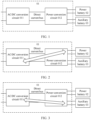
FIG. 1 is a schematic structural diagram of a charger according to an unclaimed embodiment; -
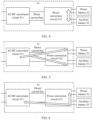
FIG. 2 is a schematic diagram of a charging mode of a charger according to an unclaimed embodiment; -
FIG. 3 is a schematic diagram of another charging mode of a charger according to an unclaimed embodiment; -
FIG. 4 is a schematic diagram of still another charging mode of a charger according to an unclaimed embodiment -
FIG. 5 is a schematic diagram of yet still another charging mode of a charger according to an unclaimed embodiment; -
FIG. 6 is a schematic diagram of a further charging mode of a charger according to an unclaimed embodiment; -
FIG. 7 is a schematic diagram of a still further charging mode of a charger according to an embodiment; -
FIG. 8 is a schematic structural diagram of a magnetic integrated device according to an unclaimed embodiment of this application; -
FIG. 9 is an equivalent circuit diagram of a magnetic integrated device according to an unclaimed embodiment of this application; -
FIG. 10 is a schematic structural diagram of another magnetic integrated device according to an embodiment of this application; -
FIG. 11 is an equivalent circuit diagram of another magnetic integrated device according to an embodiment of this application; -
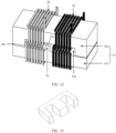
FIG. 12 is a schematic structural diagram of still another magnetic integrated device according to an embodiment of this application; -
FIG. 13 is a schematic structural diagram of a magnet according to an unclaimed embodiment; -
FIG. 14 is a schematic structural diagram of another magnet according to an embodiment of this application; -
FIG. 15 is a schematic structural diagram of still another magnet according to an unclaimed embodiment; -
FIG. 16 is a circuit diagram of a power conversion circuit according to an unclaimed embodiment; -
FIG. 17 is a circuit diagram of another power conversion circuit according to an unclaimed embodiment; -
FIG. 18 is a circuit diagram of still another power conversion circuit according to an unclaimed embodiment; -
FIG. 19 is a circuit diagram of yet another power conversion circuit according to an unclaimed embodiment; and -
FIG. 20 is a circuit diagram of a still yet power conversion circuit according to an unclaimed embodiment. - The following describes in detail a magnetic integrated device provided in embodiments of this application with reference to accompanying drawings.
-
FIG. 1 is a schematic structural diagram of a charger according to an unclaimed embodiment. As shown inFIG. 1 , thecharger 01 may include an alternating current/direct current (AC/DC)conversion circuit 011 and apower conversion circuit 012. Thepower conversion circuit 012 may also be referred to as a DCDC power converter. One end of the AC/DC may be connected to an alternating current power supply, the other end may be connected to a direct current bus, and the direct current bus is connected to thepower conversion circuit 012. - To improve power density, as shown in
FIG. 1 , theDCDC power converter 012 used in thecharger 01 may be a three-port DCDC power converter. Three ports of theDCDC power converter 012 may be respectively configured to connect to the direct current bus, apower battery 02, and anauxiliary battery 03, and theDCDC power converter 012 can convert power between any two ports. Thepower battery 02 may be configured to supply power to a drive motor of a power driven device. A voltage of thepower battery 02 is relatively high, and is generally 300 V to 600 V. Therefore, thepower battery 02 may also be referred to as a high-voltage battery. Theauxiliary battery 03 may be configured to supply power to another power driven device (for example, an electronic braking system, a dashboard, and a light control system of an electric vehicle) in the power driven device. A voltage of theauxiliary battery 03 is relatively low, and is generally 12 V to 15 V. Therefore, theauxiliary battery 03 may also be referred to as a low-voltage battery. - The
DCDC power converter 012 can convert power between any two ports. Therefore, as shown inFIG. 2 , thecharger 01 integrated with theDCDC power converter 012 can implement bidirectional power supply between the alternating current power supply and thepower battery 02. Alternatively, as shown inFIG. 3 , thecharger 01 may implement bidirectional power supply between the alternating current power supply and theauxiliary battery 03. Alternatively, as shown inFIG. 4 , thecharger 01 may implement bidirectional power supply between thepower battery 02 and theauxiliary battery 03. Alternatively, as shown inFIG. 5 , thecharger 01 may implement that the alternating current power supply supplies power to both thepower battery 02 and theauxiliary battery 03. Alternatively, as shown inFIG. 6 , thecharger 01 may implement that theauxiliary battery 03 supplies power to both the alternating current power supply and thepower battery 02. Alternatively, as shown inFIG. 7 , thecharger 01 may implement that thepower battery 02 supplies power to both the alternating current power supply and theauxiliary battery 03. - In this unclaimed embodiment, to improve power conversion efficiency and power density of the
DCDC power converter 012, theDCDC power converter 012 may be a resonant or quasi-resonant three-port DCDC power converter. In addition, to further reduce a size of a device, improve power density, improve an inter-adjustment feature of the power converter, and improve a voltage stabilizing capability of the power converter, a resonant inductor and a transformer in the resonant or quasi-resonant three-port DCDC power converter may be implemented by using a magnetic integrated device. - Optionally, the
charger 01 provided in this unclaimed embodiment may be an on-board charger (OBC) applied to the electric vehicle. Alternatively, thecharger 01 may be further applied to another power driven device, for example, a sweeping robot. -
FIG. 8 is a schematic structural diagram of a magnetic integrated device according to an unclaimed embodiment of this application. The magnetic integrated device may be applied to a power conversion circuit, for example, thepower conversion circuit 012 shown in any one ofFIG. 1 to FIG. 7 . Referring toFIG. 8 , the magnetic integrated device includes amagnetic core 10, a first transformer winding 20, and a second transformer winding 30. - A
window 100 is disposed in themagnetic core 10, and the first transformer winding 20 and the second transformer winding 30 respectively pass through thewindow 100 and are wound around themagnetic core 10. For example, as shown inFIG. 8 , thewindow 100 may be a through groove disposed in themagnetic core 10. - The first transformer winding 20 and the second transformer winding 30 are separated and wound on the
magnetic core 10, and afirst air gap 10a is formed at separation. - A magnetic line generated by the first transformer winding 20 and a magnetic line generated by the second transformer winding 30 may pass through the
first air gap 10a to form leakage inductance, and the leakage inductance may be equivalent to resonant inductance in the power conversion circuit. Therefore, there is no need to separately dispose an inductor winding in the magnetic integrated device. This effectively reduces a volume and a weight of the magnetic integrated device. - For example,
FIG. 9 is an equivalent circuit diagram of a magnetic integrated device according to an unclaimed embodiment of this application. It can be seen fromFIG. 9 that the first transformer winding 20 and the second transformer winding 30 may be equivalent to one two-port power converter. In addition, the leakage inductance formed by thefirst air gap 10a between the first transformer winding 20 and the second transformer winding 30 may be equivalent to a resonant inductor L0 connected in series to the second transformer winding 30. - In conclusion, the unclaimed embodiments provide a magnetic integrated device. The two transformer windings in the magnetic integrated device may be separated and wound, and the first air gap is formed at separation. The magnetic line may pass through the first air gap to form the leakage inductance, and the leakage inductance may be equivalent to the resonant inductance in the power conversion circuit. Therefore, there is no need to separately dispose the inductor winding in the magnetic integrated device. This effectively reduces the volume and the weight of the magnetic integrated device. In addition, the power conversion circuit that uses the magnetic integrated device also has a relatively small volume and relatively high power density.
- Optionally,
FIG. 10 is a schematic structural diagram of another magnetic integrated device according to an embodiment of this application. As shown inFIG. 10 , the magnetic integrated device may further include a third transformer winding 40. The third transformer winding 40 may pass through thewindow 100 and be wound around themagnetic core 10. - Correspondingly, the first transformer winding 20, the second transformer winding 30, and the third transformer winding 40 may be equivalent to one three-port power converter.
- Optionally, as shown in
FIG. 10 , the third transformer winding 40 and the second transformer winding 30 may be wound in a laminated manner. To be specific, the third transformer winding 40 and the second transformer winding 30 may be wound in a same-core manner. A winding manner of winding in the laminated manner can reduce occupied space of the transformer windings. This can effectively reduce the volume of the magnetic integrated device. -
FIG. 11 is an equivalent circuit diagram of a magnetic integrated device when a second transformer winding and a third transformer winding are wound in a laminated manner according to an embodiment of this application. It can be seen fromFIG. 11 that this winding manner can ensure that the third transformer winding 40 and the second transformer winding 30 are tightly coupled, and there is no leakage inductance between the two transformer windings or there is only relatively small leakage inductance between the two transformer windings. This can effectively reduce power transmission losses between the two transformer windings, and further improve power transmission efficiency between the two transformer windings. - Certainly, the third transformer winding 40 may alternatively be separated from and wound around the second transformer winding 30 or the first transformer winding 20. For example, the first transformer winding 20, the second transformer winding 30, and the third transformer winding 40 may be separated and wound on the
magnetic core 10 in sequence. A winding position of the third transformer winding 40 is not limited in this embodiment of this application. - In this embodiment of this application, one of the first transformer winding 20 and the second transformer winding 30 may be a winding configured to connect to a direct current bus, and the other winding may be a winding configured to connect to a
power battery 02 or anauxiliary battery 03. -
FIG. 12 is a schematic structural diagram of still another magnetic integrated device according to an embodiment of this application. It can be seen fromFIG. 8 ,FIG. 10 , andFIG. 12 that both a quantity of turns of the first transformer winding 20 and a quantity of turns of the second transformer winding 30 may be greater than a quantity of turns of the third transformer winding 40. To be specific, the third transformer winding 40 may be a winding configured to connect to anauxiliary battery 03 with a relatively low voltage. - Optionally, the first transformer winding 20 may be configured to connect to a
power battery 02, and the second transformer winding 30 may be configured to connect to the direct current bus. It can be seen fromFIG. 11 that, when the third transformer winding 40 and the second transformer winding 30 are wound in the laminated manner, the third transformer winding 40 (namely, a winding on a side of the auxiliary battery 03) may skip the resonant inductor L0 and be directly coupled to the direct current bus. - A voltage of the direct current bus is relatively stable. Therefore, it can be ensured that a voltage of the winding on the side of the
auxiliary battery 03 is also relatively stable. This avoids impact of the resonant inductor L0 on a voltage on a low-voltage side, and reduces a voltage fluctuation range on the low-voltage side. In this way, voltage regulation pressure of a post-stage DCDC voltage stabilizing circuit is reduced. - In this embodiment of this application, the third transformer winding 40 may be configured to connect to the
auxiliary battery 03, and a current in the third transformer winding 40 is relatively small. Therefore, as shown inFIG. 10 , both a wire width of the first transformer winding 20 and a wire width of the second transformer winding 30 may be less than a wire width of the third transformer winding 40. To be specific, the wire width of the third transformer winding 40 may be a relatively large value, and resistance may be a relatively small value. This can effectively reduce a voltage drop of the third transformer winding 40. - For example, still referring to
FIG. 10 , the third transformer winding 40 may be flat, to be specific, the third transformer winding 40 may be of a bent laminated structure, and the quantity of turns of the third transformer winding 40 may be equal to 1 or 2. The third transformer winding 40 may cover a surface of the second transformer winding 30, to be specific, the third transformer winding 40 may be wound on a side that is of the second transformer winding 30 and that is away from themagnetic core 10. For example, the flat third transformer winding 40 may cover a part of the surface of the second transformer winding 30, and a wiring terminal of the second transformer winding 30 may not be covered by the third transformer winding 40, to facilitate connection to an external circuit. - The third transformer winding 40 has a relatively small quantity of turns and a relatively large wire width, but the second transformer winding 30 has a relatively large quantity of turns and a relatively small wire width. Therefore, the third transformer winding 40 is wound on the side that is of the second transformer winding 30 and that is away from the
magnetic core 10. To be specific, the third transformer winding 40 is wound on an outer side of the second transformer winding 30, to facilitate winding of each winding and connection of a post-stage circuit. - As shown in
FIG. 10 andFIG. 12 , themagnetic core 10 includes afirst magnet 101 and asecond magnet 102. A groove or grooves is disposed in one or each of thefirst magnet 101 and thesecond magnet 102. In other words, the groove is formed in at least one of the two magnets. Thefirst magnet 101 and thesecond magnet 102 are disposed opposite to each other and enclose thewindow 100. In addition, thefirst magnet 101 and thesecond magnet 102 may be bonded and fastened. - For example, it can be seen from
FIG. 10 andFIG. 12 that one groove may be formed in thesecond magnet 102, to be specific, thesecond magnet 102 is a U-shaped magnet. No groove is formed in thefirst magnet 101, and thefirst magnet 101 may be located on a side on which the groove is formed in thesecond magnet 102, to enclose thewindow 100 with thesecond magnet 102. - In this embodiment of this application, it can be seen from
FIG. 10 andFIG. 12 that each transformer winding in the magnetic integrated device may be wound around thefirst magnet 101 and thesecond magnet 102. For example, referring toFIG. 12 , the first transformer winding 20, the second transformer winding 30, and the third transformer winding 40 included in the magnetic integrated device are respectively wound around thefirst magnet 101 and thesecond magnet 102. In addition, a part that is of the second transformer winding 30 and that is wound around each magnet is covered by the third transformer winding 40. - Optionally, a quantity of turns of each transformer winding in the magnetic integrated device wound around the
first magnet 101 may be equal to or close to a quantity of turns of each transformer winding wound around thesecond magnet 102. For example, a difference between the quantities of turns of each transformer winding wound around the two magnets may be less than a turn quantity threshold, and the turn quantity threshold may be 2 or 5. This is not limited in this embodiment of this application. - This ensures symmetry of an overall structure of the magnetic integrated device by setting the quantities of turns of each transformer winding wound around the two magnets to be equal or close.
- It should be noted that, in this embodiment of this application, the quantity of turns of each transformer winding may be a sum of the quantities of turns of the transformer winding wound around the two magnets.
- Optionally, as shown in
FIG. 8 ,FIG. 10 , andFIG. 12 , thewindow 100 formed in themagnetic core 10 may be a rectangular window. To be specific, an orthographic projection shape of thewindow 100 on a plane on which an opening of thewindow 100 is located may be a rectangle. Certainly, thewindow 100 may alternatively be a circular window or another polygon window. A shape of the window is not limited in this embodiment of this application. - It should be further noted that, in this embodiment of this application, the
magnetic core 10 may alternatively be an integrated part disposed with a through groove. For example, referring toFIG. 8 , themagnetic core 10 may be of a cube structure in which the through groove is disposed. To be specific, themagnetic core 10 may be of a "square" shape structure. The through groove is formed as thewindow 100. - Referring to
FIG. 10 andFIG. 12 , the magnetic integrated device includes amagnetic pillar 50. Themagnetic pillar 50 is located in thewindow 100, and located between the first transformer winding 20 and the second transformer winding 30. One side of themagnetic pillar 50 comes in contact with themagnetic core 10, and there is a gap between the other side and themagnetic core 10. The gap is thefirst air gap 10a between the first transformer winding 20 and the second transformer winding 30. - As shown in
FIG. 10 andFIG. 12 , themagnetic pillar 50 is located on a side that is of thefirst magnet 101 and that is close to thesecond magnet 102, and there is a gap between themagnetic pillar 50 and thesecond magnet 102. - Alternatively, the
magnetic pillar 50 is located on a side that is of thesecond magnet 102 and that is close to thefirst magnet 101, and there is a gap between themagnetic pillar 50 and thefirst magnet 101. - Alternatively, the magnetic integrated device may include two
magnetic pillars 50. One of themagnetic pillars 50 is located on a side that is of thefirst magnet 101 and that is close to thesecond magnet 102, and the othermagnetic pillar 50 is located on a side that is of thesecond magnet 102 and that is close to thefirst magnet 101. In addition, there is a gap between the twomagnetic pillars 50, to ensure that thefirst air gap 10a may be formed between the first transformer winding 20 and the second transformer winding 30. - For example, the
magnetic pillar 50 may be of a cube structure. In addition, a volume of themagnetic pillar 50 may be adjusted based on a requirement for a value of the resonant inductance in the power conversion circuit to which the magnetic integrated device is applied, to adjust a size of the gap (namely, thefirst air gap 10a) between themagnetic pillar 50 and themagnetic core 10, so as to adjust the leakage inductance of the magnetic integrated device. - For example, when the volume of the
magnetic pillar 50 is relatively small, and the gap between themagnetic pillar 50 and themagnetic core 10 is relatively large, the leakage inductance of the magnetic integrated device is relatively large. When the volume of themagnetic pillar 50 is relatively large, and the gap between themagnetic pillar 50 and themagnetic core 10 is relatively small, the leakage sensation of the magnetic integrated device is relatively small. - According to an embodiment of the invention, the
magnetic pillar 50 and themagnetic core 10 may be an integrated structure. In other words, themagnetic pillar 50 and themagnetic core 10 may be integrally formed. For example, as shown inFIG. 10 andFIG. 12 , themagnetic pillar 50 and thefirst magnet 101 may be of a T-shaped integrated structure. - In this embodiment of this application, as shown in
FIG. 10 andFIG. 12 , one or moresecond air gaps 10b may be further disposed at one end of themagnetic core 10, and thesecond air gap 10b may be connected to thewindow 100. - The
second air gap 10b may be disposed at the end that is of themagnetic core 10 and that is close to the first transformer winding 20 or at one end that is of themagnetic core 10 and that is close to the second transformer winding 30. Alternatively, thesecond air gaps 10b may be disposed at both ends of themagnetic core 10. - For example, in the magnetic integrated device shown in
FIG. 10 andFIG. 12 , onesecond air gap 10b may be disposed at the end that is of themagnetic core 10 and that is close to the first transformer winding 20. Thesecond air gap 10b may be formed by a gap between thefirst magnet 101 and thesecond magnet 102. - By disposing the
second air gap 10b on themagnetic core 10, on one hand, a magnetic permeability of themagnetic core 10 can be reduced, and on the other hand, a magnetic saturation phenomenon under a large alternating current signal or a direct current bias can be avoided, to better control inductance of the magnetic integrated device. - In conclusion, the embodiments of this application provide a magnetic integrated device. The two transformer windings in the magnetic integrated device may be separated and wound, and the first air gap is formed at separation. The magnetic line may pass through the first air gap to form the leakage inductance, and the leakage inductance may be equivalent to the resonant inductance in the power conversion circuit. Therefore, there is no need to separately dispose the inductor winding in the magnetic integrated device. This effectively reduces the volume and the weight of the magnetic integrated device. In addition, the power conversion circuit that uses the magnetic integrated device also has the relatively small volume and the relatively high power density, and the power conversion circuit has a relatively good inter-adjustment feature and a relatively high voltage stabilizing capability.
-
FIG. 16 is a circuit diagram of a power conversion circuit according to an unclaimed embodiment.. As shown inFIG. 16 , the power conversion circuit may include the magneticintegrated device 001 provided in the foregoing embodiments. The magneticintegrated device 001 may be the magnetic integrated device shown inFIG. 8 ,FIG. 10 , orFIG. 12 . Referring toFIG. 16 , the power conversion circuit may have at least two ports A and B. In other words, the power conversion circuit may be at least a two-port power conversion circuit. In the magneticintegrated device 001, a first transformer winding 20 may be connected to the first port A of the power conversion circuit, and a second transformer winding 30 may be connected to the second port B of the power conversion circuit. In addition, the first transformer winding 20 and the second transformer winding 30 are capable of transferring energy to each other through electromagnetic mutual inductance, and convert power. - Optionally, referring to
FIG. 16 , the power conversion circuit may further include a third port C, and the magneticintegrated device 001 may further include a third transformer winding 40. The third transformer winding 40 may be connected to the third port C. - In addition, the third transformer winding 40 and the first transformer winding 20 are capable of transferring energy to each other through electromagnetic mutual inductance, and convert power. The third transformer winding 40 and the second transformer winding 30 are also capable of transferring energy to each other through electromagnetic mutual inductance, and convert power.
- Optionally, as shown in
FIG. 16 , the power conversion circuit may further include threechopper subcircuits 002. Eachchopper subcircuit 002 may be separately connected to one port and one transformer winding in the magneticintegrated device 001. To be specific, each transformer winding may be connected to one port of the power conversion circuit by using onechopper subcircuit 002. - For example, referring to
FIG. 16 , it is assumed that the first port A of the power conversion circuit is configured to connect to a power battery, the second port B is configured to connect to a direct current bus, and the third port C is configured to connect to an auxiliary battery. In this case, each of thechopper subcircuit 002 connected between the first port A and the first transformer winding 20 and thechopper subcircuit 002 connected between the second port B and the second transformer winding 30 may be a bridge rectifier circuit, and the bridge rectifier circuit may include four switch devices connected in a bridge manner. Thechopper subcircuit 002 connected between the third port C and the third transformer winding 40 may be a double half-wave rectifier circuit including two switch devices, or may be a bridge rectifier circuit. - The switch device included in the
chopper subcircuit 002 may be a metal-oxide-semiconductor field-effect transistor (MOSFET), an insulated gate bipolar transistor (IGBT), a gallium nitride (GaN)-based high-electron-mobility transistor (HEMT), or the like, and the MOSFET may be a silicon carbide (SiC) MOSFET or the like. - Optionally, still referring to
FIG. 16 , the power conversion circuit may further include three filter capacitors C0. Each filter capacitor C0 may be connected in parallel to an input terminal of onechopper subcircuit 002. - In this unclaimed embodiment, the power conversion circuit may further include a resonant element, and the resonant element may be connected to the magnetic
integrated device 001, to constitute a resonant circuit. To be specific, the power conversion circuit may be a resonant or quasi-resonant power conversion circuit. - In an optional implementation, as shown in
FIG. 17 , the resonant element may include a capacitor C1, and the capacitor C1 may be connected in series to the first transformer winding 20 or the second transformer winding 30 in the magneticintegrated device 001. For example, in the circuit diagram shown inFIG. 17 , the capacitor C1 and the second transformer winding 30 are connected in series. - A power conversion circuit using this structure may be referred to as an LLC resonant power conversion circuit, or may be referred to as a series-parallel resonant power conversion circuit. L represents an inductor, and C represents a capacitor.
- In another optional implementation, as shown in
FIG. 18 , the resonant element may include a first capacitor C2 and a second capacitor C3. The first capacitor C2 may be connected in series to the first transformer winding 20 in the magneticintegrated device 001, and the second capacitor C3 may be connected in series to the second transformer winding 30 in the magneticintegrated device 001. - A power conversion circuit using this structure may also be referred to as a CLLC resonant power conversion circuit.
- In still another optional implementation, as shown in
FIG. 19 , the resonant element may include a capacitor C4 and an inductor L1. The capacitor C4 may be connected in series to the first transformer winding 20 or the second transformer winding 30 in the magneticintegrated device 001, and the inductor L1 may be connected in parallel to the first transformer winding 20 or the second transformer winding 30. For example, in a structure shown inFIG. 19 , the capacitor C4 is connected in series to the second transformer winding 30, and the inductor L1 is connected in parallel to the second transformer winding 30. - A power conversion circuit using this structure may be referred to as an L-LLC resonant power conversion circuit.
- In yet another optional implementation, as shown in
FIG. 16 , no additional resonant element may be disposed in the power conversion circuit, and the leakage inductance in the magnetic integrated device may be equivalent to two resonant inductors L0. The two resonant inductors L0 are respectively connected in series to the first transformer winding 20 and the second transformer winding 30. A power conversion circuit using this structure may also be referred to as a dual active full bridge (DAB) power conversion circuit. - In conclusion, the unclaimed embodiments provide a power conversion circuit. In the magnetic integrated device used in the power conversion circuit, the two transformer windings may be separated and wound, and a first air gap is formed at separation. A magnetic line may pass through the first air gap to form leakage inductance, and the leakage inductance may be equivalent to resonant inductance in the power conversion circuit. Therefore, there is no need to separately dispose an inductor winding in the magnetic integrated device. This effectively reduces a volume and a weight of the magnetic integrated device. In addition, the power conversion circuit that uses the magnetic integrated device has a relatively small volume and relatively high power density.
-
FIG. 20 is a circuit diagram of still yet power conversion circuit according to an embodiment of this application. As shown inFIG. 20 , the power conversion circuit has three ports: A, B, and C. In other words, the power conversion circuit is a three-port power conversion circuit. The power conversion circuit may include aresonant element 003, a first transformer T1, and a second transformer T2. - A primary side of the first transformer T1 may be connected in series to the
resonant element 003 and the first transformer T1 and theresonant element 003 that are connected in series may be connected to the second port B of the three ports, and a secondary side of the first transformer T1 may be connected to the first port A of the three ports. - A primary side of the second transformer T2 may be connected in parallel to the first transformer T1 and the
resonant element 003 that are connected in series. For example, in a structure shown inFIG. 20 , theresonant element 003 may be an inductor L2. In addition, the primary side of the second transformer T2 is further connected to the second port B of the three ports, and a secondary side of the second transformer T2 may be connected to the third port C of the three ports. - The first transformer T1 and the
resonant element 003 are connected in series, and then connected in parallel to the primary side of the second transformer T2. Therefore, impact of theresonant element 003 on an output voltage of the secondary side of the second transformer T2 can be avoided. This ensures that a fluctuation range of the output voltage of the secondary side of the second transformer T2 is relatively small, stability of the output voltage is relatively high, and voltage regulation pressure of a post-stage circuit is further reduced. - It can be learned from the foregoing analysis that in this embodiment of this application, a discrete device may be further used to implement a topology of a power conversion circuit using a magnetic integrated device.
- Optionally, the second port B of the power conversion circuit may be configured to connect to a direct current bus, the first port A may be configured to connect to a power battery, and the third port C may be configured to connect to an auxiliary battery.
- It should be noted that, in addition to the
resonant element 003, the power conversion circuit may further include another resonant element, for example, an inductor and a capacitor, to implement a topology of the power conversion circuit shown in any one ofFIG. 16 to FIG. 19 . Details are not described in this unclaimed embodiment of this application. - An unclaimed embodiment further provides a charger. As shown in
FIG. 1 to FIG. 7 , the charger may include the alternating current/directcurrent conversion circuit 011 and thepower conversion circuit 012. Thepower conversion circuit 012 may be the circuit shown in any one ofFIG. 16 to FIG. 20 . A second port B of thepower conversion circuit 012 may be connected to the alternating current/directcurrent conversion circuit 011, for example, may be connected to the alternating current/directcurrent conversion circuit 011 by using the direct current bus. - Optionally, the charger may be applied to an electric vehicle, or may be applied to another power driven device, for example, a sweeping robot.
- An unclaimed embodiment further provides an electric vehicle. Referring to
FIG. 1 to FIG. 7 , the electric vehicle may include thepower battery 02, theauxiliary battery 03, and thecharger 01. Thecharger 01 may be separately connected to thepower battery 02 and theauxiliary battery 03. For example, a first port A of thepower conversion circuit 012 included in thecharger 01 may be connected to thepower battery 02, and a third port C of thepower conversion circuit 012 included in thecharger 01 may be connected to theauxiliary battery 03. - Optionally, the electric vehicle may be an electric automobile, an electric motorcycle, an electric bicycle, or the like. This is not limited in this unclaimed embodiment.
- The Scope of the invention is only defined by the appended claims and any example not being an embodiment of the invention thus defined shall be regarded only for illustrating purposes.
Claims (11)
- A magnetic integrated device, comprising a magnetic core (10), a first transformer winding (20), and a second transformer winding (30), whereina window (100) is disposed in the magnetic core (10), and the first transformer winding (20) and the second transformer winding (30) respectively pass through the window (100) and are wound around the magnetic core (10);wherein the magnetic core (10) comprises a first piece (101) and a second piece (102) disposed opposite to each other and enclosing the window (100);the first transformer winding (20) and the second transformer winding (30) are separated and each wound around both the first piece (101) and the second piece (102),the first piece (101) being a I-shaped piece and the second piece (102) being a U-shape piece comprising a groove in the second piece (102);wherein a first part of the first transformer winding (20) and a first part of the second transformer winding (30) are both wounded around the second piece (102) in the groove of the second piece (102), a second part of the first transformer winding (20) and a second part of the second transformer winding (30) are both wounded around the first piece (101), a first winding axis of the first part of the first transformer winding (20) and a second winding axis of the first part of the second transformer winding (30) are aligned, and a third winding axis of the second part of the first transformer winding (20) and a fourth winding axis of the second part of the second transformer winding (30) are aligned;wherein the magnetic integrated device further comprises a magnetic pillar (50) that is located in the window (100) and located between the first transformer winding (20) and the second transformer winding (30); andwherein the magnetic pillar (50) is located on a side of first piece (101) or on a side of the second piece (102) and a first side of the magnetic pillar (50) comes in contact with the magnetic core (10) on the side on which it is located, and there is a gap between the opposite side to the first side of the magnetic pillar (50) and the magnetic core (10).
- The magnetic integrated device according to claim 1, further comprising a third transformer winding (40), wherein the third transformer winding (40) passes through the window (100) and is wound around the magnetic core (10).
- The magnetic integrated device according to claim 2, wherein the third transformer winding (40) and the second transformer winding (30) are wound in a laminated manner.
- The magnetic integrated device according to claim 3, wherein the third transformer winding (40) is flat, and the third transformer winding (40) covers a surface of the second transformer winding (30).
- The magnetic integrated device according to claim 4, wherein the third transformer winding (40) covers a part of the surface of the second transformer winding (30), and a wiring terminal of the second transformer winding (30) is not covered by the third transformer winding (40).
- The magnetic integrated device according to any one of claims 2 to 5, wherein both a quantity of turns of the first transformer winding (20) and a quantity of turns of the second transformer winding (30) are greater than a quantity of turns of the third transformer winding (40).
- The magnetic integrated device according to claim 6, wherein both a wire width of the first transformer winding (20) and a wire width of the second transformer winding (30) are less than a wire width of the third transformer winding (40).
- The magnetic integrated device according to claim 1, wherein the magnetic pillar (50) and the magnetic core (10) are of an integrated structure.
- The magnetic integrated device according to any of the preceding claims, wherein a quantity of turns of each transformer winding wound around the first piece (101) is equal to a quantity of turns of each transformer winding wound around the second piece (102).
- The magnetic integrated device according to any one of claims 1 to 11, wherein one end of the magnetic core (10) is disposed with one or more second air gaps (10b), and the second air gap (10b) is connected to the window (100).
- The magnetic integrated device according to any one of claims 1 to 10, wherein the window (100) is a rectangular window.
Applications Claiming Priority (2)
| Application Number | Priority Date | Filing Date | Title |
|---|---|---|---|
| CN201910750681.6A CN110634655B (en) | 2019-08-14 | 2019-08-14 | Magnetic integrated devices, power conversion circuits, chargers and electric vehicles |
| PCT/CN2020/089871 WO2021027348A1 (en) | 2019-08-14 | 2020-05-12 | Magnetic integrated device, power conversion circuit, charger, and electric vehicle |
Publications (3)
| Publication Number | Publication Date |
|---|---|
| EP3923307A1 EP3923307A1 (en) | 2021-12-15 |
| EP3923307A4 EP3923307A4 (en) | 2022-11-09 |
| EP3923307B1 true EP3923307B1 (en) | 2025-07-09 |
Family
ID=68969871
Family Applications (1)
| Application Number | Title | Priority Date | Filing Date |
|---|---|---|---|
| EP20852993.3A Active EP3923307B1 (en) | 2019-08-14 | 2020-05-12 | Magnetic integrated device, power conversion circuit, charger, and electric vehicle |
Country Status (5)
| Country | Link |
|---|---|
| US (1) | US11527354B2 (en) |
| EP (1) | EP3923307B1 (en) |
| CN (1) | CN110634655B (en) |
| BR (1) | BR112021014228A2 (en) |
| WO (1) | WO2021027348A1 (en) |
Families Citing this family (7)
| Publication number | Priority date | Publication date | Assignee | Title |
|---|---|---|---|---|
| CN109686538B (en) * | 2018-12-11 | 2020-07-28 | 华为技术有限公司 | Transformer and power supply |
| CN110634655B (en) * | 2019-08-14 | 2021-05-14 | 华为技术有限公司 | Magnetic integrated devices, power conversion circuits, chargers and electric vehicles |
| CN110460242B (en) * | 2019-09-12 | 2020-11-10 | 台达电子企业管理(上海)有限公司 | Bidirectional isolation type resonant converter |
| CN111899976B (en) * | 2020-08-26 | 2024-06-25 | 福州大学 | Wide-range control method and structure for leakage inductance of transformer |
| CN112600287B (en) * | 2020-10-16 | 2022-12-09 | 国网湖南省电力有限公司 | Impedance matching type power transmission line energy taking device with air gap adjusting function and application method thereof |
| CN113012908B (en) * | 2021-03-01 | 2022-03-29 | 杭州富特科技股份有限公司 | Integrated magnetic components and integrated magnetic component systems based on power equipment |
| CN112563000B (en) * | 2021-03-01 | 2021-05-07 | 杭州富特科技股份有限公司 | Integrated magnetic device and converter |
Citations (1)
| Publication number | Priority date | Publication date | Assignee | Title |
|---|---|---|---|---|
| CN107633936A (en) * | 2017-08-30 | 2018-01-26 | 杭州富特科技股份有限公司 | LLC transformers and its implementation and core assembly |
Family Cites Families (12)
| Publication number | Priority date | Publication date | Assignee | Title |
|---|---|---|---|---|
| JPH0865904A (en) * | 1994-06-06 | 1996-03-08 | Nippondenso Co Ltd | Charger for electric vehicle |
| FR2730849B1 (en) * | 1995-02-20 | 1997-05-09 | Actia | TRANSFORMER, PARTICULARLY FOR AN ENERGY CONVERTER, AND A RESONANCE ENERGY CONVERTER HAVING SUCH A TRANSFORMER |
| US20100067263A1 (en) * | 2008-06-16 | 2010-03-18 | Northeastern University | Dual interleaved flyback converter for high input voltage |
| CN101355308B (en) * | 2008-08-29 | 2010-07-21 | 浙江大学 | A magnetically integrated zero-voltage and zero-current soft-switching full-bridge circuit |
| CN101720160A (en) * | 2009-09-15 | 2010-06-02 | 杨东平 | Driving circuit of cold cathode fluorescence lamp |
| EP2677526B1 (en) * | 2012-06-22 | 2017-09-27 | DET International Holding Limited | Integrated magnetics for switched mode power converter |
| CN103595367B (en) * | 2013-11-07 | 2017-03-08 | 华为技术有限公司 | A kind of magnetic integrated device and a kind of circuit for power conversion |
| CN105761880B (en) * | 2016-04-20 | 2017-12-29 | 华为技术有限公司 | A kind of thin film inductor and power-switching circuit |
| CN108109821A (en) * | 2017-12-06 | 2018-06-01 | 深圳威迈斯电源有限公司 | A kind of highly integrated magnetic cell |
| CN108736734B (en) * | 2018-07-10 | 2023-10-13 | 珠海英搏尔电气股份有限公司 | A resonant converter |
| CN110040028A (en) * | 2019-04-15 | 2019-07-23 | 创驱(上海)新能源科技有限公司 | A kind of integral control circuit of Vehicular charger and DCDC conversion equipment |
| CN110634655B (en) * | 2019-08-14 | 2021-05-14 | 华为技术有限公司 | Magnetic integrated devices, power conversion circuits, chargers and electric vehicles |
-
2019
- 2019-08-14 CN CN201910750681.6A patent/CN110634655B/en active Active
-
2020
- 2020-05-12 WO PCT/CN2020/089871 patent/WO2021027348A1/en not_active Ceased
- 2020-05-12 EP EP20852993.3A patent/EP3923307B1/en active Active
- 2020-05-12 BR BR112021014228A patent/BR112021014228A2/en not_active Application Discontinuation
-
2022
- 2022-01-28 US US17/588,202 patent/US11527354B2/en active Active
Patent Citations (1)
| Publication number | Priority date | Publication date | Assignee | Title |
|---|---|---|---|---|
| CN107633936A (en) * | 2017-08-30 | 2018-01-26 | 杭州富特科技股份有限公司 | LLC transformers and its implementation and core assembly |
Also Published As
| Publication number | Publication date |
|---|---|
| BR112021014228A2 (en) | 2022-04-19 |
| US20220157516A1 (en) | 2022-05-19 |
| WO2021027348A1 (en) | 2021-02-18 |
| CN110634655B (en) | 2021-05-14 |
| EP3923307A1 (en) | 2021-12-15 |
| CN110634655A (en) | 2019-12-31 |
| EP3923307A4 (en) | 2022-11-09 |
| US11527354B2 (en) | 2022-12-13 |
Similar Documents
| Publication | Publication Date | Title |
|---|---|---|
| EP3923307B1 (en) | Magnetic integrated device, power conversion circuit, charger, and electric vehicle | |
| US12027986B2 (en) | Magnetic integration of three-phase resonant converter and accessory power supply | |
| Ramachandran et al. | Experimental demonstration of a 98.8% efficient isolated DC–DC GaN converter | |
| Steigerwald et al. | A comparison of high-power DC-DC soft-switched converter topologies | |
| US8659272B2 (en) | Bidirectional boost-buck DC-DC converter | |
| EP2677526B1 (en) | Integrated magnetics for switched mode power converter | |
| US9356520B2 (en) | Forward converter with magnetic component | |
| WO2021047207A1 (en) | Magnetic device and bidirectional dc converter | |
| US11270832B2 (en) | Integrated magnetic device and direct current-direct current converter | |
| CN109036800B (en) | Three-phase magnetic integrated device | |
| US11095227B2 (en) | Interleaved LLC resonant converter | |
| CN112970079B (en) | Reactors and multi-phase interleaved DC-DC converters | |
| JP2007508000A (en) | Ripple current reduction for transformers | |
| US20220223331A1 (en) | Compact power inductor | |
| Ou et al. | A novel transformer structure used in a 1.4 MHz LLC resonant converter with GaNFETs | |
| WO2012072732A2 (en) | A method for increasing power transferred by an integrated inductor and a resonant-mode power supply with an integrated inductor | |
| US20160218524A1 (en) | Circuit Arrangement Having Charge Storage Units | |
| US20210082609A1 (en) | Common-mode/differential-mode throttle for an electrically driveable motor vehicle | |
| KR100732612B1 (en) | High Efficiency Step-Down DC-DC Converters for Hybrid Vehicles | |
| TWI894659B (en) | Power transformer, circuit board, and manufacturing method of transformer | |
| KR102735137B1 (en) | Downsized variable inductor | |
| CN223957439U (en) | Magnetic coupling-based double BUCK three-port bidirectional conversion circuit and device thereof | |
| US20250196665A1 (en) | Integrated power module for electric vehicle | |
| JP5303493B2 (en) | Inductors, transformers and switching power supplies | |
| CN103680867A (en) | Side-winding type winding transformer and winding method thereof |
Legal Events
| Date | Code | Title | Description |
|---|---|---|---|
| STAA | Information on the status of an ep patent application or granted ep patent |
Free format text: STATUS: THE INTERNATIONAL PUBLICATION HAS BEEN MADE |
|
| PUAI | Public reference made under article 153(3) epc to a published international application that has entered the european phase |
Free format text: ORIGINAL CODE: 0009012 |
|
| STAA | Information on the status of an ep patent application or granted ep patent |
Free format text: STATUS: REQUEST FOR EXAMINATION WAS MADE |
|
| 17P | Request for examination filed |
Effective date: 20210908 |
|
| AK | Designated contracting states |
Kind code of ref document: A1 Designated state(s): AL AT BE BG CH CY CZ DE DK EE ES FI FR GB GR HR HU IE IS IT LI LT LU LV MC MK MT NL NO PL PT RO RS SE SI SK SM TR |
|
| A4 | Supplementary search report drawn up and despatched |
Effective date: 20221012 |
|
| RIC1 | Information provided on ipc code assigned before grant |
Ipc: H02M 3/22 20060101ALI20221006BHEP Ipc: H01F 27/00 20060101AFI20221006BHEP |
|
| DAV | Request for validation of the european patent (deleted) | ||
| DAX | Request for extension of the european patent (deleted) | ||
| STAA | Information on the status of an ep patent application or granted ep patent |
Free format text: STATUS: EXAMINATION IS IN PROGRESS |
|
| 17Q | First examination report despatched |
Effective date: 20230320 |
|
| GRAP | Despatch of communication of intention to grant a patent |
Free format text: ORIGINAL CODE: EPIDOSNIGR1 |
|
| STAA | Information on the status of an ep patent application or granted ep patent |
Free format text: STATUS: GRANT OF PATENT IS INTENDED |
|
| INTG | Intention to grant announced |
Effective date: 20250226 |
|
| GRAS | Grant fee paid |
Free format text: ORIGINAL CODE: EPIDOSNIGR3 |
|
| GRAA | (expected) grant |
Free format text: ORIGINAL CODE: 0009210 |
|
| STAA | Information on the status of an ep patent application or granted ep patent |
Free format text: STATUS: THE PATENT HAS BEEN GRANTED |
|
| AK | Designated contracting states |
Kind code of ref document: B1 Designated state(s): AL AT BE BG CH CY CZ DE DK EE ES FI FR GB GR HR HU IE IS IT LI LT LU LV MC MK MT NL NO PL PT RO RS SE SI SK SM TR |
|
| P01 | Opt-out of the competence of the unified patent court (upc) registered |
Free format text: CASE NUMBER: APP_25648/2025 Effective date: 20250528 |
|
| REG | Reference to a national code |
Ref country code: GB Ref legal event code: FG4D |
|
| REG | Reference to a national code |
Ref country code: CH Ref legal event code: EP |
|
| REG | Reference to a national code |
Ref country code: IE Ref legal event code: FG4D |
|
| REG | Reference to a national code |
Ref country code: DE Ref legal event code: R096 Ref document number: 602020054341 Country of ref document: DE |
|
| REG | Reference to a national code |
Ref country code: NL Ref legal event code: MP Effective date: 20250709 |
|
| PG25 | Lapsed in a contracting state [announced via postgrant information from national office to epo] |
Ref country code: PT Free format text: LAPSE BECAUSE OF FAILURE TO SUBMIT A TRANSLATION OF THE DESCRIPTION OR TO PAY THE FEE WITHIN THE PRESCRIBED TIME-LIMIT Effective date: 20251110 |
|
| PG25 | Lapsed in a contracting state [announced via postgrant information from national office to epo] |
Ref country code: NL Free format text: LAPSE BECAUSE OF FAILURE TO SUBMIT A TRANSLATION OF THE DESCRIPTION OR TO PAY THE FEE WITHIN THE PRESCRIBED TIME-LIMIT Effective date: 20250709 |
|
| REG | Reference to a national code |
Ref country code: AT Ref legal event code: MK05 Ref document number: 1812695 Country of ref document: AT Kind code of ref document: T Effective date: 20250709 |
|
| PG25 | Lapsed in a contracting state [announced via postgrant information from national office to epo] |
Ref country code: IS Free format text: LAPSE BECAUSE OF FAILURE TO SUBMIT A TRANSLATION OF THE DESCRIPTION OR TO PAY THE FEE WITHIN THE PRESCRIBED TIME-LIMIT Effective date: 20251109 |
|
| PG25 | Lapsed in a contracting state [announced via postgrant information from national office to epo] |
Ref country code: NO Free format text: LAPSE BECAUSE OF FAILURE TO SUBMIT A TRANSLATION OF THE DESCRIPTION OR TO PAY THE FEE WITHIN THE PRESCRIBED TIME-LIMIT Effective date: 20251009 |
|
| REG | Reference to a national code |
Ref country code: LT Ref legal event code: MG9D |
|
| PG25 | Lapsed in a contracting state [announced via postgrant information from national office to epo] |
Ref country code: AT Free format text: LAPSE BECAUSE OF FAILURE TO SUBMIT A TRANSLATION OF THE DESCRIPTION OR TO PAY THE FEE WITHIN THE PRESCRIBED TIME-LIMIT Effective date: 20250709 |
|
| PG25 | Lapsed in a contracting state [announced via postgrant information from national office to epo] |
Ref country code: FI Free format text: LAPSE BECAUSE OF FAILURE TO SUBMIT A TRANSLATION OF THE DESCRIPTION OR TO PAY THE FEE WITHIN THE PRESCRIBED TIME-LIMIT Effective date: 20250709 |
|
| PG25 | Lapsed in a contracting state [announced via postgrant information from national office to epo] |
Ref country code: HR Free format text: LAPSE BECAUSE OF FAILURE TO SUBMIT A TRANSLATION OF THE DESCRIPTION OR TO PAY THE FEE WITHIN THE PRESCRIBED TIME-LIMIT Effective date: 20250709 |
|
| PG25 | Lapsed in a contracting state [announced via postgrant information from national office to epo] |
Ref country code: GR Free format text: LAPSE BECAUSE OF FAILURE TO SUBMIT A TRANSLATION OF THE DESCRIPTION OR TO PAY THE FEE WITHIN THE PRESCRIBED TIME-LIMIT Effective date: 20251010 |
|
| PG25 | Lapsed in a contracting state [announced via postgrant information from national office to epo] |
Ref country code: SE Free format text: LAPSE BECAUSE OF FAILURE TO SUBMIT A TRANSLATION OF THE DESCRIPTION OR TO PAY THE FEE WITHIN THE PRESCRIBED TIME-LIMIT Effective date: 20250709 |
|
| PG25 | Lapsed in a contracting state [announced via postgrant information from national office to epo] |
Ref country code: LV Free format text: LAPSE BECAUSE OF FAILURE TO SUBMIT A TRANSLATION OF THE DESCRIPTION OR TO PAY THE FEE WITHIN THE PRESCRIBED TIME-LIMIT Effective date: 20250709 |
|
| PG25 | Lapsed in a contracting state [announced via postgrant information from national office to epo] |
Ref country code: BG Free format text: LAPSE BECAUSE OF FAILURE TO SUBMIT A TRANSLATION OF THE DESCRIPTION OR TO PAY THE FEE WITHIN THE PRESCRIBED TIME-LIMIT Effective date: 20250709 Ref country code: PL Free format text: LAPSE BECAUSE OF FAILURE TO SUBMIT A TRANSLATION OF THE DESCRIPTION OR TO PAY THE FEE WITHIN THE PRESCRIBED TIME-LIMIT Effective date: 20250709 |
|
| PG25 | Lapsed in a contracting state [announced via postgrant information from national office to epo] |
Ref country code: RS Free format text: LAPSE BECAUSE OF FAILURE TO SUBMIT A TRANSLATION OF THE DESCRIPTION OR TO PAY THE FEE WITHIN THE PRESCRIBED TIME-LIMIT Effective date: 20251009 |
|
| PG25 | Lapsed in a contracting state [announced via postgrant information from national office to epo] |
Ref country code: ES Free format text: LAPSE BECAUSE OF FAILURE TO SUBMIT A TRANSLATION OF THE DESCRIPTION OR TO PAY THE FEE WITHIN THE PRESCRIBED TIME-LIMIT Effective date: 20250709 |
|
| PG25 | Lapsed in a contracting state [announced via postgrant information from national office to epo] |
Ref country code: SM Free format text: LAPSE BECAUSE OF FAILURE TO SUBMIT A TRANSLATION OF THE DESCRIPTION OR TO PAY THE FEE WITHIN THE PRESCRIBED TIME-LIMIT Effective date: 20250709 |
|
| PG25 | Lapsed in a contracting state [announced via postgrant information from national office to epo] |
Ref country code: DK Free format text: LAPSE BECAUSE OF FAILURE TO SUBMIT A TRANSLATION OF THE DESCRIPTION OR TO PAY THE FEE WITHIN THE PRESCRIBED TIME-LIMIT Effective date: 20250709 |
|
| PG25 | Lapsed in a contracting state [announced via postgrant information from national office to epo] |
Ref country code: IT Free format text: LAPSE BECAUSE OF FAILURE TO SUBMIT A TRANSLATION OF THE DESCRIPTION OR TO PAY THE FEE WITHIN THE PRESCRIBED TIME-LIMIT Effective date: 20250709 |
|
| PG25 | Lapsed in a contracting state [announced via postgrant information from national office to epo] |
Ref country code: CZ Free format text: LAPSE BECAUSE OF FAILURE TO SUBMIT A TRANSLATION OF THE DESCRIPTION OR TO PAY THE FEE WITHIN THE PRESCRIBED TIME-LIMIT Effective date: 20250709 |
|
| PG25 | Lapsed in a contracting state [announced via postgrant information from national office to epo] |
Ref country code: SK Free format text: LAPSE BECAUSE OF FAILURE TO SUBMIT A TRANSLATION OF THE DESCRIPTION OR TO PAY THE FEE WITHIN THE PRESCRIBED TIME-LIMIT Effective date: 20250709 Ref country code: EE Free format text: LAPSE BECAUSE OF FAILURE TO SUBMIT A TRANSLATION OF THE DESCRIPTION OR TO PAY THE FEE WITHIN THE PRESCRIBED TIME-LIMIT Effective date: 20250709 |