EP3923048A1 - Beam delivery system - Google Patents
Beam delivery system Download PDFInfo
- Publication number
- EP3923048A1 EP3923048A1 EP21177257.9A EP21177257A EP3923048A1 EP 3923048 A1 EP3923048 A1 EP 3923048A1 EP 21177257 A EP21177257 A EP 21177257A EP 3923048 A1 EP3923048 A1 EP 3923048A1
- Authority
- EP
- European Patent Office
- Prior art keywords
- beam delivery
- waveguide
- outputs
- integrated circuit
- delivery system
- Prior art date
- Legal status (The legal status is an assumption and is not a legal conclusion. Google has not performed a legal analysis and makes no representation as to the accuracy of the status listed.)
- Granted
Links
Images




Classifications
-
- G—PHYSICS
- G06—COMPUTING OR CALCULATING; COUNTING
- G06E—OPTICAL COMPUTING DEVICES
- G06E3/00—Devices not provided for in group G06E1/00, e.g. for processing analogue or hybrid data
- G06E3/001—Analogue devices in which mathematical operations are carried out with the aid of optical or electro-optical elements
- G06E3/005—Analogue devices in which mathematical operations are carried out with the aid of optical or electro-optical elements using electro-optical or opto-electronic means
-
- G—PHYSICS
- G02—OPTICS
- G02B—OPTICAL ELEMENTS, SYSTEMS OR APPARATUS
- G02B6/00—Light guides; Structural details of arrangements comprising light guides and other optical elements, e.g. couplings
- G02B6/10—Light guides; Structural details of arrangements comprising light guides and other optical elements, e.g. couplings of the optical waveguide type
- G02B6/12—Light guides; Structural details of arrangements comprising light guides and other optical elements, e.g. couplings of the optical waveguide type of the integrated circuit kind
- G02B6/122—Basic optical elements, e.g. light-guiding paths
- G02B6/125—Bends, branchings or intersections
-
- G—PHYSICS
- G02—OPTICS
- G02F—OPTICAL DEVICES OR ARRANGEMENTS FOR THE CONTROL OF LIGHT BY MODIFICATION OF THE OPTICAL PROPERTIES OF THE MEDIA OF THE ELEMENTS INVOLVED THEREIN; NON-LINEAR OPTICS; FREQUENCY-CHANGING OF LIGHT; OPTICAL LOGIC ELEMENTS; OPTICAL ANALOGUE/DIGITAL CONVERTERS
- G02F1/00—Devices or arrangements for the control of the intensity, colour, phase, polarisation or direction of light arriving from an independent light source, e.g. switching, gating or modulating; Non-linear optics
- G02F1/29—Devices or arrangements for the control of the intensity, colour, phase, polarisation or direction of light arriving from an independent light source, e.g. switching, gating or modulating; Non-linear optics for the control of the position or the direction of light beams, i.e. deflection
-
- G—PHYSICS
- G02—OPTICS
- G02F—OPTICAL DEVICES OR ARRANGEMENTS FOR THE CONTROL OF LIGHT BY MODIFICATION OF THE OPTICAL PROPERTIES OF THE MEDIA OF THE ELEMENTS INVOLVED THEREIN; NON-LINEAR OPTICS; FREQUENCY-CHANGING OF LIGHT; OPTICAL LOGIC ELEMENTS; OPTICAL ANALOGUE/DIGITAL CONVERTERS
- G02F1/00—Devices or arrangements for the control of the intensity, colour, phase, polarisation or direction of light arriving from an independent light source, e.g. switching, gating or modulating; Non-linear optics
- G02F1/29—Devices or arrangements for the control of the intensity, colour, phase, polarisation or direction of light arriving from an independent light source, e.g. switching, gating or modulating; Non-linear optics for the control of the position or the direction of light beams, i.e. deflection
- G02F1/292—Devices or arrangements for the control of the intensity, colour, phase, polarisation or direction of light arriving from an independent light source, e.g. switching, gating or modulating; Non-linear optics for the control of the position or the direction of light beams, i.e. deflection by controlled diffraction or phased-array beam steering
-
- G—PHYSICS
- G02—OPTICS
- G02F—OPTICAL DEVICES OR ARRANGEMENTS FOR THE CONTROL OF LIGHT BY MODIFICATION OF THE OPTICAL PROPERTIES OF THE MEDIA OF THE ELEMENTS INVOLVED THEREIN; NON-LINEAR OPTICS; FREQUENCY-CHANGING OF LIGHT; OPTICAL LOGIC ELEMENTS; OPTICAL ANALOGUE/DIGITAL CONVERTERS
- G02F1/00—Devices or arrangements for the control of the intensity, colour, phase, polarisation or direction of light arriving from an independent light source, e.g. switching, gating or modulating; Non-linear optics
- G02F1/29—Devices or arrangements for the control of the intensity, colour, phase, polarisation or direction of light arriving from an independent light source, e.g. switching, gating or modulating; Non-linear optics for the control of the position or the direction of light beams, i.e. deflection
- G02F1/295—Analog deflection from or in an optical waveguide structure]
-
- G—PHYSICS
- G02—OPTICS
- G02F—OPTICAL DEVICES OR ARRANGEMENTS FOR THE CONTROL OF LIGHT BY MODIFICATION OF THE OPTICAL PROPERTIES OF THE MEDIA OF THE ELEMENTS INVOLVED THEREIN; NON-LINEAR OPTICS; FREQUENCY-CHANGING OF LIGHT; OPTICAL LOGIC ELEMENTS; OPTICAL ANALOGUE/DIGITAL CONVERTERS
- G02F1/00—Devices or arrangements for the control of the intensity, colour, phase, polarisation or direction of light arriving from an independent light source, e.g. switching, gating or modulating; Non-linear optics
- G02F1/29—Devices or arrangements for the control of the intensity, colour, phase, polarisation or direction of light arriving from an independent light source, e.g. switching, gating or modulating; Non-linear optics for the control of the position or the direction of light beams, i.e. deflection
- G02F1/295—Analog deflection from or in an optical waveguide structure]
- G02F1/2955—Analog deflection from or in an optical waveguide structure] by controlled diffraction or phased-array beam steering
-
- G—PHYSICS
- G02—OPTICS
- G02B—OPTICAL ELEMENTS, SYSTEMS OR APPARATUS
- G02B6/00—Light guides; Structural details of arrangements comprising light guides and other optical elements, e.g. couplings
- G02B6/10—Light guides; Structural details of arrangements comprising light guides and other optical elements, e.g. couplings of the optical waveguide type
- G02B6/12—Light guides; Structural details of arrangements comprising light guides and other optical elements, e.g. couplings of the optical waveguide type of the integrated circuit kind
- G02B2006/12133—Functions
- G02B2006/1215—Splitter
-
- G—PHYSICS
- G02—OPTICS
- G02B—OPTICAL ELEMENTS, SYSTEMS OR APPARATUS
- G02B6/00—Light guides; Structural details of arrangements comprising light guides and other optical elements, e.g. couplings
- G02B6/10—Light guides; Structural details of arrangements comprising light guides and other optical elements, e.g. couplings of the optical waveguide type
- G02B6/12—Light guides; Structural details of arrangements comprising light guides and other optical elements, e.g. couplings of the optical waveguide type of the integrated circuit kind
- G02B2006/12166—Manufacturing methods
- G02B2006/12176—Etching
-
- G—PHYSICS
- G02—OPTICS
- G02B—OPTICAL ELEMENTS, SYSTEMS OR APPARATUS
- G02B6/00—Light guides; Structural details of arrangements comprising light guides and other optical elements, e.g. couplings
- G02B6/10—Light guides; Structural details of arrangements comprising light guides and other optical elements, e.g. couplings of the optical waveguide type
- G02B6/12—Light guides; Structural details of arrangements comprising light guides and other optical elements, e.g. couplings of the optical waveguide type of the integrated circuit kind
- G02B6/12002—Three-dimensional structures
-
- G—PHYSICS
- G02—OPTICS
- G02B—OPTICAL ELEMENTS, SYSTEMS OR APPARATUS
- G02B6/00—Light guides; Structural details of arrangements comprising light guides and other optical elements, e.g. couplings
- G02B6/10—Light guides; Structural details of arrangements comprising light guides and other optical elements, e.g. couplings of the optical waveguide type
- G02B6/12—Light guides; Structural details of arrangements comprising light guides and other optical elements, e.g. couplings of the optical waveguide type of the integrated circuit kind
- G02B6/12007—Light guides; Structural details of arrangements comprising light guides and other optical elements, e.g. couplings of the optical waveguide type of the integrated circuit kind forming wavelength selective elements, e.g. multiplexer, demultiplexer
- G02B6/12009—Light guides; Structural details of arrangements comprising light guides and other optical elements, e.g. couplings of the optical waveguide type of the integrated circuit kind forming wavelength selective elements, e.g. multiplexer, demultiplexer comprising arrayed waveguide grating [AWG] devices, i.e. with a phased array of waveguides
- G02B6/12014—Light guides; Structural details of arrangements comprising light guides and other optical elements, e.g. couplings of the optical waveguide type of the integrated circuit kind forming wavelength selective elements, e.g. multiplexer, demultiplexer comprising arrayed waveguide grating [AWG] devices, i.e. with a phased array of waveguides characterised by the wavefront splitting or combining section, e.g. grooves or optical elements in a slab waveguide
-
- G—PHYSICS
- G02—OPTICS
- G02B—OPTICAL ELEMENTS, SYSTEMS OR APPARATUS
- G02B6/00—Light guides; Structural details of arrangements comprising light guides and other optical elements, e.g. couplings
- G02B6/10—Light guides; Structural details of arrangements comprising light guides and other optical elements, e.g. couplings of the optical waveguide type
- G02B6/12—Light guides; Structural details of arrangements comprising light guides and other optical elements, e.g. couplings of the optical waveguide type of the integrated circuit kind
- G02B6/12007—Light guides; Structural details of arrangements comprising light guides and other optical elements, e.g. couplings of the optical waveguide type of the integrated circuit kind forming wavelength selective elements, e.g. multiplexer, demultiplexer
- G02B6/12009—Light guides; Structural details of arrangements comprising light guides and other optical elements, e.g. couplings of the optical waveguide type of the integrated circuit kind forming wavelength selective elements, e.g. multiplexer, demultiplexer comprising arrayed waveguide grating [AWG] devices, i.e. with a phased array of waveguides
- G02B6/12016—Light guides; Structural details of arrangements comprising light guides and other optical elements, e.g. couplings of the optical waveguide type of the integrated circuit kind forming wavelength selective elements, e.g. multiplexer, demultiplexer comprising arrayed waveguide grating [AWG] devices, i.e. with a phased array of waveguides characterised by the input or output waveguides, e.g. tapered waveguide ends, coupled together pairs of output waveguides
-
- G—PHYSICS
- G02—OPTICS
- G02B—OPTICAL ELEMENTS, SYSTEMS OR APPARATUS
- G02B6/00—Light guides; Structural details of arrangements comprising light guides and other optical elements, e.g. couplings
- G02B6/10—Light guides; Structural details of arrangements comprising light guides and other optical elements, e.g. couplings of the optical waveguide type
- G02B6/12—Light guides; Structural details of arrangements comprising light guides and other optical elements, e.g. couplings of the optical waveguide type of the integrated circuit kind
- G02B6/12007—Light guides; Structural details of arrangements comprising light guides and other optical elements, e.g. couplings of the optical waveguide type of the integrated circuit kind forming wavelength selective elements, e.g. multiplexer, demultiplexer
- G02B6/12009—Light guides; Structural details of arrangements comprising light guides and other optical elements, e.g. couplings of the optical waveguide type of the integrated circuit kind forming wavelength selective elements, e.g. multiplexer, demultiplexer comprising arrayed waveguide grating [AWG] devices, i.e. with a phased array of waveguides
- G02B6/12019—Light guides; Structural details of arrangements comprising light guides and other optical elements, e.g. couplings of the optical waveguide type of the integrated circuit kind forming wavelength selective elements, e.g. multiplexer, demultiplexer comprising arrayed waveguide grating [AWG] devices, i.e. with a phased array of waveguides characterised by the optical interconnection to or from the AWG devices, e.g. integration or coupling with lasers or photodiodes
-
- G—PHYSICS
- G02—OPTICS
- G02B—OPTICAL ELEMENTS, SYSTEMS OR APPARATUS
- G02B6/00—Light guides; Structural details of arrangements comprising light guides and other optical elements, e.g. couplings
- G02B6/10—Light guides; Structural details of arrangements comprising light guides and other optical elements, e.g. couplings of the optical waveguide type
- G02B6/12—Light guides; Structural details of arrangements comprising light guides and other optical elements, e.g. couplings of the optical waveguide type of the integrated circuit kind
- G02B6/12007—Light guides; Structural details of arrangements comprising light guides and other optical elements, e.g. couplings of the optical waveguide type of the integrated circuit kind forming wavelength selective elements, e.g. multiplexer, demultiplexer
- G02B6/12009—Light guides; Structural details of arrangements comprising light guides and other optical elements, e.g. couplings of the optical waveguide type of the integrated circuit kind forming wavelength selective elements, e.g. multiplexer, demultiplexer comprising arrayed waveguide grating [AWG] devices, i.e. with a phased array of waveguides
- G02B6/12033—Light guides; Structural details of arrangements comprising light guides and other optical elements, e.g. couplings of the optical waveguide type of the integrated circuit kind forming wavelength selective elements, e.g. multiplexer, demultiplexer comprising arrayed waveguide grating [AWG] devices, i.e. with a phased array of waveguides characterised by means for configuring the device, e.g. moveable element for wavelength tuning
-
- G—PHYSICS
- G02—OPTICS
- G02B—OPTICAL ELEMENTS, SYSTEMS OR APPARATUS
- G02B6/00—Light guides; Structural details of arrangements comprising light guides and other optical elements, e.g. couplings
- G02B6/10—Light guides; Structural details of arrangements comprising light guides and other optical elements, e.g. couplings of the optical waveguide type
- G02B6/12—Light guides; Structural details of arrangements comprising light guides and other optical elements, e.g. couplings of the optical waveguide type of the integrated circuit kind
- G02B6/122—Basic optical elements, e.g. light-guiding paths
- G02B6/1228—Tapered waveguides, e.g. integrated spot-size transformers
-
- G—PHYSICS
- G02—OPTICS
- G02B—OPTICAL ELEMENTS, SYSTEMS OR APPARATUS
- G02B6/00—Light guides; Structural details of arrangements comprising light guides and other optical elements, e.g. couplings
- G02B6/24—Coupling light guides
- G02B6/26—Optical coupling means
-
- G—PHYSICS
- G06—COMPUTING OR CALCULATING; COUNTING
- G06N—COMPUTING ARRANGEMENTS BASED ON SPECIFIC COMPUTATIONAL MODELS
- G06N10/00—Quantum computing, i.e. information processing based on quantum-mechanical phenomena
- G06N10/40—Physical realisations or architectures of quantum processors or components for manipulating qubits, e.g. qubit coupling or qubit control
Definitions
- At least one of the plurality of waveguide outputs is directed to a photodetector.
- the first waveguide layer and the second waveguide layer are comprised of different materials.
- a beam delivery system comprises a beam delivery photonic integrated circuit comprising, a plurality of optical inputs, a plurality of waveguide outputs, wherein the plurality of waveguide outputs are tapered, a plurality of beam paths, each beam path connecting one of the plurality of waveguide outputs to only one of the plurality of waveguide inputs, wherein the beam delivery photonic integrated circuit is on a chip, an optical relay assembly, the optical relay assembly configured to receive beams provided by at least two of the plurality of waveguide outputs and focus each received beam on a corresponding plurality of positions of an atomic object confinement apparatus.
- the plurality of beam paths are defined lithographically.
- Figure 1 provides a schematic diagram of an example trapped atomic object quantum computer system 100, in accordance with an example embodiment.
- the quantum computer system 100 comprises a computing entity 10 and a quantum computer 110.
- a controller 30 of the quantum computer 110 may be in communication with the computing entity 10 via one or more wired and/or wireless networks 20.
- the quantum computer 110 comprises the controller 30, a cryo and/or vacuum chamber 40 enclosing a atomic object confinement apparatus 50 (e.g., an ion trap and/or the like), one or more manipulation sources, one or more laser systems 70, and/or the like.
- a atomic object confinement apparatus 50 e.g., an ion trap and/or the like
- the controller 30 is configured to control the atomic object confinement apparatus 50, cooling and/or vacuum systems (not shown) controlling the temperature and pressure within the cryo and/or vacuum chamber 40, manipulation sources, laser system 70, servo, and/or other components of the quantum computer 110 (e.g., an optical collection system configured for "reading" the output of the quantum computer).
- the controller 30 is configured to control various components of the quantum computer 110 in accordance with executable instructions, command sets, and/or the like provided by the computing entity 10 and/or generated by the controller 30.
- the controller 30 is configured to receive output from the quantum computer 110 (e.g., from an optical collection system) and provide the output and/or the result of processing the output to the computing entity 10.
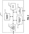
- the controller 30 may comprise various controller elements including processing element(s) 205, memory 210, driver controller elements 215, a communication interface 220, analog-digital converter 225, and/or the like.
- the processing element(s) 205 may comprise programmable logic devices (CPLDs), microprocessors, coprocessing entities, application-specific instruction-set processors (ASIPs), integrated circuits, application specific integrated circuits (ASICs), field programmable gate arrays (FPGAs), programmable logic arrays (PLAs), hardware accelerators, other processing devices and/or circuitry, and/or the like, and/or controllers.
- the term circuitry may refer to an entirely hardware embodiment or a combination of hardware and computer program products.
- the processing element(s) 205 of the controller 30 comprises a clock and/or is in communication with a clock.
- the memory 210 may store qubit records corresponding the qubits of quantum computer (e.g., in a qubit record data store, qubit record database, qubit record table, and/or the like), a calibration table, an executable queue, computer program code (e.g., in a one or more computer languages, specialized controller language(s), and/or the like), and/or the like.
- qubit records corresponding the qubits of quantum computer (e.g., in a qubit record data store, qubit record database, qubit record table, and/or the like), a calibration table, an executable queue, computer program code (e.g., in a one or more computer languages, specialized controller language(s), and/or the like), and/or the like.
- the controller 30 comprises means for communicating and/or receiving signals from one or more optical receiver components such as cameras, MEMs cameras, CCD cameras, photodiodes, photomultiplier tubes, and/or the like.
- the controller 30 may comprise one or more analog-digital converter element(s) 225 configured to receive signals from one or more optical receiver components, calibration sensors, and/or the like.
- the controller 30 may comprise a communication interface 220 for interfacing and/or communicating with a computing entity 10.
- the controller 30 may comprise a communication interface 220 for receiving executable instructions, command sets, and/or the like from the computing entity 10 and providing output received from the quantum computer 110 (e.g., from an optical collection system) and/or the result of a processing the output to the computing entity 10.
- the computing entity 10 and the controller 30 may communicate via a direct wired and/or wireless connection and/or one or more wired and/or wireless networks 20.
- the computing entity 10 may be configured to receive and/or provide communications using a wired data transmission protocol, such as fiber distributed data interface (FDDI), digital subscriber line (DSL), Ethernet, asynchronous transfer mode (ATM), frame relay, data over cable service interface specification (DOCSIS), or any other wired transmission protocol.
- a wired data transmission protocol such as fiber distributed data interface (FDDI), digital subscriber line (DSL), Ethernet, asynchronous transfer mode (ATM), frame relay, data over cable service interface specification (DOCSIS), or any other wired transmission protocol.
- FDDI fiber distributed data interface
- DSL digital subscriber line
- Ethernet asynchronous transfer mode
- ATM asynchronous transfer mode
- frame relay frame relay
- DOCSIS data over cable service interface specification
- the computing entity 10 may use such protocols and standards to communicate using Border Gateway Protocol (BGP), Dynamic Host Configuration Protocol (DHCP), Domain Name System (DNS), File Transfer Protocol (FTP), Hypertext Transfer Protocol (HTTP), HTTP over TLS/SSL/Secure, Internet Message Access Protocol (IMAP), Network Time Protocol (NTP), Simple Mail Transfer Protocol (SMTP), Telnet, Transport Layer Security (TLS), Secure Sockets Layer (SSL), Internet Protocol (IP), Transmission Control Protocol (TCP), User Datagram Protocol (UDP), Datagram Congestion Control Protocol (DCCP), Stream Control Transmission Protocol (SCTP), HyperText Markup Language (HTML), and/or the like.
- Border Gateway Protocol BGP
- Dynamic Host Configuration Protocol DHCP
- DNS Domain Name System
- FTP File Transfer Protocol
- HTTP Hypertext Transfer Protocol
- HTTP Hypertext Transfer Protocol
- HTTP HyperText Transfer Protocol
- HTTP HyperText Markup Language
- IP Internet Protocol
- TCP Transmission Control Protocol
- UDP User Datagram Protocol
- DCCP
- the computing entity 10 can communicate with various other entities using concepts such as Unstructured Supplementary Service information/data (USSD), Short Message Service (SMS), Multimedia Messaging Service (MMS), Dual-Tone Multi-Frequency Signaling (DTMF), and/or Subscriber Identity Module Dialer (SIM dialer).
- USSD Unstructured Supplementary Service information/data
- SMS Short Message Service
- MMS Multimedia Messaging Service
- DTMF Dual-Tone Multi-Frequency Signaling
- SIM dialer Subscriber Identity Module Dialer
- the computing entity 10 can also download changes, add-ons, and updates, for instance, to its firmware, software (e.g., including executable instructions, applications, program modules), and operating system.
- the computing entity 10 may also comprise a user interface device comprising one or more user input/output interfaces (e.g., a display 316 and/or speaker/speaker driver coupled to a processing element(s) 308 and a touch screen, keyboard, mouse, and/or microphone coupled to a processing element(s) 308).
- the user output interface may be configured to provide an application, browser, user interface, interface, dashboard, screen, webpage, page, and/or similar words used herein interchangeably executing on and/or accessible via the computing entity 10 to cause display or audible presentation of information/data and for interaction therewith via one or more user input interfaces.
- the computing entity 10 can also include volatile memory or storage 322 and/or non-volatile memory or storage 324, which can be embedded and/or may be removable.
- the non-volatile memory may be ROM, PROM, EPROM, EEPROM, flash memory, MMCs, SD memory cards, Memory Sticks, CBRAM, PRAM, FeRAM, RRAM, SONOS, racetrack memory, and/or the like.
- the volatile memory may be RAM, DRAM, SRAM, FPM DRAM, EDO DRAM, SDRAM, DDR SDRAM, DDR2 SDRAM, DDR3 SDRAM, RDRAM, RIMM, DIMM, SIMM, VRAM, cache memory, register memory, and/or the like.
- a beam delivery photonic integrated circuit 400 may have one or more inputs and has a plurality of outputs.
- the input(s) and outputs may be connected by waveguides fabricated on a chip, which may be lithographically fabricated on a chip.
- the beam paths connecting the input(s) and outputs as well as the spacing of the input(s) and outputs may be defined lithographically.
- the outputs may be a dense set of outputs for output of parallel laser beams.
- the dense set of outputs may be on a single chip and may allow for the positions of the outputs to be fixed relative to each other, which may provide for greater system stability.
- a fixed spacing may eliminate the need to make individual optical path adjustments for each beam.
- a beam delivery photonic integrated circuit 400 may be located external to the vacuum chamber 40 or, alternatively, a beam delivery photonic integrated circuit may be located inside the vacuum chamber 40.
- a laser system 70 provides one or more gate signals to one or more portions of an atomic object confinement apparatus 50 having atomic objects confined and/or trapped therein for use as qubits of a quantum computer 110.
- the frequency of the laser beam may be on the order of 100 MHz to 100 GHz.
- FIG. 4 there are three stages of splitters that cascade: a first stage of splitter 420, a second stage of splitters 430A, 430B, and a third stage of splitters 440A, 440B, 440C, and 440D. While Figure 4 depicts three stages of splitters, other embodiments may have additional stages of cascaded splitters, such as having tens or hundreds of stages of splitters. Additionally, while Figure 4 depicts splitters in a single plane, the splitters may be configured in a three dimensional direction such that there may be multiple stages of cascading occurring in multiple dimensions (e.g., X, Y, or Z dimensions). Additionally, or alternatively, multiple beam delivery photonic integrated circuits 400 may be provided on one chip, which may be done by isolating in the input and outputs of each beam delivery photonic integrated circuit 400 from each other.
- multiple beam delivery photonic integrated circuits 400 may be provided on one chip, which may be done by isolating in the input and outputs of each beam delivery photonic integrated circuit
- a beam path may have an optical element.
- An optical element may allow for a beam in the beam path to be independently tuned, such as for one or more parameters, from beams in other beam paths.
- the parameters that may be tuned include frequency, phase, and/or intensity. Additional parameters are discussed herein.
- Outputs of beam delivery photonic integrated circuit 400 are provided to an optical relay assembly 500.
- the optical relay assembly 500 may be configured to provide a desired magnification, such as by configuring a pitch and/or mode-field diameter. As the number of beams from the beam delivery photonic integrated circuit 400 grows, the complexity of the optical relay assembly 500 may or may not increase. For example, the optical relay assembly 500 may be modified to address or correct field-dependent aberrations.
- Figure 5 depicts an optical relay assembly 500.
- Figure 5 illustrates an example optical relay assembly 500.
- the outputs of beam delivery photonic integrated circuit 400 are input into optical relay assembly 500.
- Figure 5 uses three different colors (e.g., 505A, 505B, and 505C), with each color representing a beam output from one output of beam delivery photonic integrated circuit.
- the first group of optical elements before the aperture stop may collect light from the photonic chip in a telecentric or non-telecentric fashion, which may depend on the designed output of the chip, and may route it to the second group of optical elements, which may create a telecentric or non-telecentric output where each beam is focused to the required location with the appropriate magnification.
- Figure 5 illustrates a plurality of optical elements at 510A-510K in optical relay assembly 500.
- a first cladding layer 704 is deposited on the substrate 702 (e.g., Si), as shown in Figures 7A and 7B .
- a first cladding layer 704 comprising oxide and/or dielectric (e.g., SiO 2 ) may be deposited on the substrate 702.
- the first cladding layer 704 may electrically and/or thermally isolate the waveguide layer 706 from the substrate 702.
- Figure 7A illustrates a cross-section before completion of step/operation 602
- Figure 7B illustrates a cross-section after completion of step 602.
- a waveguide layer 706 is deposited onto the first cladding layer 704, as shown in Figure 7C .
- the waveguide layer 706 may be thin film that is deposited.
- a waveguide layer 706 comprising the material (e.g., a dielectric material, such as Al 2 O 3 , Si 3 N 4 , HfO 2 , AlN, Ta 2 O 5 , and/or the like) of the passive waveguide layer 706 may be deposited onto the first cladding layer 704.
- Figure 7C illustrates a cross-section after completion of step 604.
- the resist layer 710 may be baked and then exposed to UV radiation to develop resist layer 710A.
- Figure 7F illustrates a cross-section after completion of step 610.
- Figure 7H illustrates a cross-section after completion of step/operation 614.
- the waveguide layer 706 is etched and/or patterned to form waveguide layer 706A.
- Figure 7I illustrates a cross-section after completion of step 616.
- Figure 7P illustrates a cross-section after completion of step/operation 630.
- cladding layer 708B is etched to form cladding layer 708C and cladding layer 704 is etched to form cladding layer 704A.
- Figure 7S illustrates a cross-section after completion of step 636.
Landscapes
- Physics & Mathematics (AREA)
- General Physics & Mathematics (AREA)
- Engineering & Computer Science (AREA)
- Nonlinear Science (AREA)
- Optics & Photonics (AREA)
- Theoretical Computer Science (AREA)
- Microelectronics & Electronic Packaging (AREA)
- Mathematical Physics (AREA)
- Data Mining & Analysis (AREA)
- Evolutionary Computation (AREA)
- Pure & Applied Mathematics (AREA)
- Computing Systems (AREA)
- General Engineering & Computer Science (AREA)
- Mathematical Analysis (AREA)
- Software Systems (AREA)
- Mathematical Optimization (AREA)
- Artificial Intelligence (AREA)
- Condensed Matter Physics & Semiconductors (AREA)
- Computational Mathematics (AREA)
- Power Engineering (AREA)
- Optical Modulation, Optical Deflection, Nonlinear Optics, Optical Demodulation, Optical Logic Elements (AREA)
- Optical Integrated Circuits (AREA)
Abstract
Description
- This application claims priority to and the benefit of
United States Provisional Patent Application No. 63/037,482, filed June 10, 2020 - Various embodiments relate to a beam delivery system, and specifically to a beam delivery system for quantum computing applications with a beam delivery photonic integrated circuit.
- In various atomic systems, it is important to be able to deliver laser beams to dense one-or-more dimensional arrays of atomic systems at precision spacings and mode profiles. For example, trapped ion quantum computing uses laser beams to complete various functions within the trapped ion quantum computer. Such applications require that the lasers are delivered to the ion trap precisely and accurately in terms of position, spacings, mode profile, polarization, frequency, and phase.
- Example embodiments provide a beam delivery element for quantum computing applications.
- According to one aspect, a beam delivery photonic integrated circuit is provided. In an example embodiment, the beam delivery system comprises a beam delivery photonic integrated circuit, which comprises one or more optical inputs, a plurality of waveguide outputs, wherein each of the plurality of waveguide outputs are tapered, a plurality of beam paths, each beam path connecting one of the plurality of waveguide outputs to at least one of the one or more optical inputs, wherein the beam delivery photonic integrated circuit is on a chip, and an optical relay assembly, the optical relay assembly configured to receive beams provided by at least two of the plurality of waveguide outputs and focus each received beam on a corresponding one of a plurality of positions of an atomic object confinement apparatus.
- In another example embodiment, the one or more of the plurality of beam paths comprises an optical element configured to tune a beam for at least one of frequency, phase, or intensity.
- In another example embodiment, at least one of the plurality of waveguide outputs is directed to a photodetector.
- In another example embodiment, the plurality of beam paths are defined lithographically.
- In another example embodiment, the plurality of waveguide outputs are located on a polished edge of the beam delivery photonic integrated circuit.
- In another example embodiment, each of the waveguide outputs are on one side of the beam delivery photonic integrated circuit and are parallel to each other.
- In another example embodiment, each of the plurality of waveguide outputs are at most 150 micrometers from the next closest of the plurality of waveguide outputs.
- In another example embodiment, the optical input is butt-coupled to an optical fiber providing an input beam.
- In another example embodiment, a beam delivery system comprises a beam delivery photonic integrated circuit, which comprises a first waveguide layer and a second waveguide layer, the first waveguide layer, which comprises a first optical input, a plurality of first waveguide outputs, wherein the plurality of first waveguide outputs are tapered, a plurality of first beam paths, each first beam path connecting one of the plurality of first waveguide outputs to the first optical input, the second waveguide layer comprises a second optical input, a plurality of second waveguide outputs, wherein the plurality of second waveguide outputs are tapered, a plurality of second beam paths, each second beam path connecting one of the plurality of second waveguide outputs to the second optical input, wherein the beam delivery photonic integrated circuit is on a chip, an optical relay assembly, the optical relay assembly configured to receive beams provided by at least one of the plurality of first waveguide outputs and at least one of the plurality of second waveguide outputs, and the optical relay assembly further configured to focus each received beam on a corresponding plurality of positions of an atomic object confinement apparatus.
- In another example embodiment, one or more of the plurality of first waveguide outputs or of the plurality of second waveguide outputs is directed to a photodetector.
- In another example embodiment, one or more of the plurality of first beam paths or the plurality of second beam paths comprises an optical element configured to tune a beam for at least one of frequency, phase, or intensity.
- In another example embodiment, the plurality of first waveguide outputs and the plurality of second waveguide outputs are located on a polished edge of the beam delivery photonic integrated circuit.
- In another example embodiment, each of the plurality of first waveguide outputs and the plurality of second waveguide outputs are on one side of the beam delivery photonic integrated circuit and are parallel to each other.
- In another example embodiment, each of the plurality of first waveguide outputs are at most 150 micrometers from the next closest of the plurality of waveguide outputs.
- In another example embodiment, at least one of the first waveguide layer or the second waveguide layer comprises a dielectric material.
- In another example embodiment, the first waveguide layer and the second waveguide layer are comprised of different materials.
- In another example embodiment, a beam delivery system comprises a beam delivery photonic integrated circuit comprising, a plurality of optical inputs, a plurality of waveguide outputs, wherein the plurality of waveguide outputs are tapered, a plurality of beam paths, each beam path connecting one of the plurality of waveguide outputs to only one of the plurality of waveguide inputs, wherein the beam delivery photonic integrated circuit is on a chip, an optical relay assembly, the optical relay assembly configured to receive beams provided by at least two of the plurality of waveguide outputs and focus each received beam on a corresponding plurality of positions of an atomic object confinement apparatus.
- In another example embodiment, one or more of the plurality of beam paths comprises an optical element configured to tune a beam for at least one of frequency, phase, or intensity.
- In another example embodiment, at least one of the plurality of waveguide outputs is directed to a photodetector.
- In another example embodiment, the plurality of beam paths are defined lithographically.
- Having thus described the invention in general terms, reference will now be made to the accompanying drawings, which are not necessarily drawn to scale, and wherein:
-
Figure 1 provides a schematic diagram of an example trapped atomic object quantum computer system, in accordance with an example embodiment. -
Figure 2 provides a schematic diagram of an example controller that may be used in accordance with an example embodiment. -
Figure 3 provides a schematic diagram of an example computing entity that may be used in accordance with an example embodiment. -
Figure 4 provides a block diagram of an example beam delivery photonic integrated circuit, in accordance with an example embodiment. -
Figure 5 illustrates an example optical relay assembly, in accordance with an example embodiment. -
Figure 6 provides a flowchart illustrating various processes, procedures, and/or operations performed in fabricating a beam delivery photonic integrated circuit, in accordance with an example embodiment. -
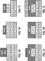
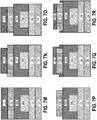
Figures 7A-7T provide cross-sectional views of various stages of fabricating a beam delivery photonic integrated circuit, in accordance with an example embodiment. - The present invention now will be described more fully hereinafter with reference to the accompanying drawings, in which some, but not all embodiments of the invention are shown. Indeed, the invention may be embodied in many different forms and should not be construed as limited to the embodiments set forth herein; rather, these embodiments are provided so that this disclosure will satisfy applicable legal requirements. The term "or" (also denoted "/") is used herein in both the alternative and conjunctive sense, unless otherwise indicated. The terms "illustrative" and "exemplary" are used to be examples with no indication of quality level. The terms "generally" and "approximately" refer to within engineering and/or manufacturing limits and/or within user measurement capabilities, unless otherwise indicated. Like numbers refer to like elements throughout.
- As described above, in various atomic systems, it is important to be able to precisely and accurately, in terms of position, spacings, mode profile, polarization, frequency, and/or phase, deliver one or more laser beams to the atomic system. For example, in atomic systems such as atomic clocks, Bose-Einstein condensate systems, trapped ion systems, and/or other atomic systems, precise and accurate laser beam delivery is important for various uses of the system, manipulating the system, and/or the like. Various example embodiments corresponding to trapped atomic object (e.g., atoms, ions) quantum computer systems will now be described in more detail.
-
Figure 1 provides a schematic diagram of an example trapped atomic objectquantum computer system 100, in accordance with an example embodiment. In various embodiments, thequantum computer system 100 comprises acomputing entity 10 and aquantum computer 110. In various embodiments, acontroller 30 of thequantum computer 110 may be in communication with thecomputing entity 10 via one or more wired and/orwireless networks 20. In various embodiments, thequantum computer 110 comprises thecontroller 30, a cryo and/orvacuum chamber 40 enclosing a atomic object confinement apparatus 50 (e.g., an ion trap and/or the like), one or more manipulation sources, one ormore laser systems 70, and/or the like. In various embodiments, the atomicobject confinement apparatus 50 is a confinement apparatus configured to atomic object confinement apparatus one or more atomic objects therein and the manipulation sources are configured to provide manipulation signals to one or more portions of the atomicobject confinement apparatus 50 via optical paths. In various embodiments, the manipulation signals may be used to initialize one or more atomic objects into a qubit space, perform cooling operations, perform measurement operations, provide one or more gate signals, and/or the like. In various embodiments, the manipulation sources comprise one ormore laser systems 70 is configured to provide one or more manipulation signals (e.g., gate signals) to one or more portions of the atomicobject confinement apparatus 50 to enact one or more quantum gates (e.g., quantum logic gates). In various embodiments, the quantum gates may be one qubit gates, two qubit gates, and/or the like. In various embodiments, the one or more gate signals may be provided to the one or more portions of the atomicobject confinement apparatus 50 via optical path(s) 68, which may include beam delivery photonicintegrated circuit 400 andoptical relay assembly 500. In various embodiments, the atomic objects confined or trapped within the atomicobject confinement apparatus 50 are ions, atoms, and/or the like. For example, in an example embodiment, an atomic object is an ytterbium ion. In an example embodiment, an atomic object comprises a qubit ion and a corresponding cooling ion. - In various embodiments, a
computing entity 10 is configured to allow a user to provide input to the quantum computer system 100 (e.g., via a user interface of the computing entity 10) and receive, view, and/or the like output from thequantum computer system 100. Thecomputing entity 10 may be in communication with thecontroller 30 via one or more wired orwireless networks 20. For example, thecomputing entity 10 may be configured to provide quantum circuits to thecontroller 30 for execution by thequantum computer 110 and thecontroller 30 may provide the results of executing one or more quantum circuits to thecomputing entity 10. - In various embodiments, the
controller 30 is configured to control the atomicobject confinement apparatus 50, cooling and/or vacuum systems (not shown) controlling the temperature and pressure within the cryo and/orvacuum chamber 40, manipulation sources,laser system 70, servo, and/or other components of the quantum computer 110 (e.g., an optical collection system configured for "reading" the output of the quantum computer). In various embodiments, thecontroller 30 is configured to control various components of thequantum computer 110 in accordance with executable instructions, command sets, and/or the like provided by thecomputing entity 10 and/or generated by thecontroller 30. In various embodiments, thecontroller 30 is configured to receive output from the quantum computer 110 (e.g., from an optical collection system) and provide the output and/or the result of processing the output to thecomputing entity 10. - In various embodiments, a
quantum computer 110 comprises acontroller 30 configured to control various elements of thequantum computer 110. In various embodiments, acontroller 30 may be configured to cause aquantum computer 110 to perform various operations (e.g., computing operations such as gate operations, cooling operations, transport operations, qubit interaction operations, qubit measurement operations, leakage suppression operations, and/or the like). For example, thecontroller 30 may be configured to cause manipulation sources to provide manipulation signals to atomic objects confined and/or trapped within the atomicobject confinement apparatus 50. For example, thecontroller 30 may be configured to cause thelaser system 70, possibly in coordination with servo system, to provide one or more gate signals to one or more atomic objects confined and/or trapped within the atomicobject confinement apparatus 50 so as to enact, for example, one or more quantum gates. In various embodiments, thecontroller 30 may be configured to control a cryogenic system and/or vacuum system controlling the temperature and pressure within the cryogenic and/orvacuum chamber 40, manipulation sources, and/or other systems controlling the environmental conditions (e.g., temperature, humidity, pressure, and/or the like) within the cryogenic and/orvacuum chamber 40 and/or configured to manipulate and/or cause a controlled evolution of quantum states of one or more atomic objects within the atomicobject confinement apparatus 50. - As shown in
Figure 2 , in various embodiments, thecontroller 30 may comprise various controller elements including processing element(s) 205,memory 210,driver controller elements 215, acommunication interface 220, analog-digital converter 225, and/or the like. For example, the processing element(s) 205 may comprise programmable logic devices (CPLDs), microprocessors, coprocessing entities, application-specific instruction-set processors (ASIPs), integrated circuits, application specific integrated circuits (ASICs), field programmable gate arrays (FPGAs), programmable logic arrays (PLAs), hardware accelerators, other processing devices and/or circuitry, and/or the like, and/or controllers. The term circuitry may refer to an entirely hardware embodiment or a combination of hardware and computer program products. In an example embodiment, the processing element(s) 205 of thecontroller 30 comprises a clock and/or is in communication with a clock. - For example, the
memory 210 may comprise non-transitory memory such as volatile and/or non-volatile memory storage such as one or more of as hard disks, ROM, PROM, EPROM, EEPROM, flash memory, MMCs, SD memory cards, Memory Sticks, CBRAM, PRAM, FeRAM, RRAM, SONOS, racetrack memory, RAM, DRAM, SRAM, FPM DRAM, EDO DRAM, SDRAM, DDR SDRAM, DDR2 SDRAM, DDR3 SDRAM, RDRAM, RIMM, DIMM, SIMM, VRAM, cache memory, register memory, and/or the like. In various embodiments, thememory 210 may store qubit records corresponding the qubits of quantum computer (e.g., in a qubit record data store, qubit record database, qubit record table, and/or the like), a calibration table, an executable queue, computer program code (e.g., in a one or more computer languages, specialized controller language(s), and/or the like), and/or the like. In an example embodiment, execution of at least a portion of the computer program code stored in the memory 210 (e.g., by a processing element(s) 205) causes thecontroller 30 to perform one or more steps, operations, processes, procedures and/or the like described herein for tracking the phase of an atomic object within an atomic system and causing the adjustment of the phase of one or more manipulation sources and/or signal(s) generated thereby. - In various embodiments, the
driver controller elements 215 may include one or more drivers and/or controller elements each configured to control one or more drivers. In various embodiments, thedriver controller elements 215 may comprise drivers and/or driver controllers. For example, the driver controllers may be configured to cause one or more corresponding drivers to be operated in accordance with executable instructions, commands, and/or the like scheduled and executed by the controller 30 (e.g., by the processing element(s) 205). In various embodiments, thedriver controller elements 215 may enable thecontroller 30 to operate alaser system 70, servo, manipulation sources, vacuum and/or cryogenic systems, and/or the like. In various embodiments, the drivers may be laser drivers; microwave drivers; vacuum component drivers; cryogenic and/or vacuum system component drivers; current drivers, and/or the like. For example, the drivers and/or driver controllers may be configured to cause a magnetic field generation device (e.g., comprising circuitry coupled to a voltage source (e.g., a current driver or voltage driver), permanent magnet(s), and/or a combination thereof) to generate a magnetic field having a particular direction and magnitude at one or more positions of the atomicobject confinement apparatus 50. In various embodiments, a plurality of positions of the atomic object confinement apparatus 50 (e.g., atomic object confinement apparatus zones) may be defined. In various embodiments, thecontroller 30 comprises means for communicating and/or receiving signals from one or more optical receiver components such as cameras, MEMs cameras, CCD cameras, photodiodes, photomultiplier tubes, and/or the like. For example, thecontroller 30 may comprise one or more analog-digital converter element(s) 225 configured to receive signals from one or more optical receiver components, calibration sensors, and/or the like. - In various embodiments, the
controller 30 may comprise acommunication interface 220 for interfacing and/or communicating with acomputing entity 10. For example, thecontroller 30 may comprise acommunication interface 220 for receiving executable instructions, command sets, and/or the like from thecomputing entity 10 and providing output received from the quantum computer 110 (e.g., from an optical collection system) and/or the result of a processing the output to thecomputing entity 10. In various embodiments, thecomputing entity 10 and thecontroller 30 may communicate via a direct wired and/or wireless connection and/or one or more wired and/orwireless networks 20. -
Figure 3 provides an illustrative schematic diagram of anexample computing entity 10 that can be used in conjunction with embodiments of the present invention. In various embodiments, acomputing entity 10 is configured to allow a user to provide input to the quantum computer 110 (e.g., via a user interface of the computing entity 10) and receive, display, analyze, and/or the like output from thequantum computer 110. For example, a user may operate acomputing entity 10 to generate and/or program a quantum algorithm and/or quantum circuit (e.g., that includes a D-state AC-Stark shift gate) that may be provided such that thecontroller 30 may receive the quantum algorithm and/or quantum circuit and cause thequantum computer 110 to perform the quantum algorithm and/or quantum circuit. - As shown in
Figure 3 , acomputing entity 10 can include anantenna 312, a transmitter 304 (e.g., radio), a receiver 306 (e.g., radio), and aprocessing element 308 that provides signals to and receives signals from thetransmitter 304 andreceiver 306, respectively, which may collectively be referred to a transceiver. The signals provided to and received from thetransmitter 304 and thereceiver 306, respectively, may include signaling information/data in accordance with an air interface standard of applicable wireless systems to communicate with various entities, such as acontroller 30,other computing entities 10, and/or the like. In this regard, thecomputing entity 10 may be capable of operating with one or more air interface standards, communication protocols, modulation types, and access types. For example, thecomputing entity 10 may be configured to receive and/or provide communications using a wired data transmission protocol, such as fiber distributed data interface (FDDI), digital subscriber line (DSL), Ethernet, asynchronous transfer mode (ATM), frame relay, data over cable service interface specification (DOCSIS), or any other wired transmission protocol. Similarly, thecomputing entity 10 may be configured to communicate via wireless external communication networks using any of a variety of protocols, such as general packet radio service (GPRS), Universal Mobile Telecommunications System (UMTS), Code Division Multiple Access 2000 (CDMA2000), CDMA2000 1X (1xRTT), Wideband Code Division Multiple Access (WCDMA), Global System for Mobile Communications (GSM), Enhanced Data rates for GSM Evolution (EDGE), Time Division-Synchronous Code Division Multiple Access (TD-SCDMA), Long Term Evolution (LTE), Evolved Universal Terrestrial Radio Access Network (E-UTRAN), Evolution-Data Optimized (EVDO), High Speed Packet Access (HSPA), High-Speed Downlink Packet Access (HSDPA), IEEE 802.11 (Wi-Fi), Wi-Fi Direct, 802.16 (WiMAX), ultra wideband (UWB), infrared (IR) protocols, near field communication (NFC) protocols, Wibree, Bluetooth protocols, wireless universal serial bus (USB) protocols, and/or any other wireless protocol. Thecomputing entity 10 may use such protocols and standards to communicate using Border Gateway Protocol (BGP), Dynamic Host Configuration Protocol (DHCP), Domain Name System (DNS), File Transfer Protocol (FTP), Hypertext Transfer Protocol (HTTP), HTTP over TLS/SSL/Secure, Internet Message Access Protocol (IMAP), Network Time Protocol (NTP), Simple Mail Transfer Protocol (SMTP), Telnet, Transport Layer Security (TLS), Secure Sockets Layer (SSL), Internet Protocol (IP), Transmission Control Protocol (TCP), User Datagram Protocol (UDP), Datagram Congestion Control Protocol (DCCP), Stream Control Transmission Protocol (SCTP), HyperText Markup Language (HTML), and/or the like. - Via these communication standards and protocols, the
computing entity 10 can communicate with various other entities using concepts such as Unstructured Supplementary Service information/data (USSD), Short Message Service (SMS), Multimedia Messaging Service (MMS), Dual-Tone Multi-Frequency Signaling (DTMF), and/or Subscriber Identity Module Dialer (SIM dialer). Thecomputing entity 10 can also download changes, add-ons, and updates, for instance, to its firmware, software (e.g., including executable instructions, applications, program modules), and operating system. - The
computing entity 10 may also comprise a user interface device comprising one or more user input/output interfaces (e.g., adisplay 316 and/or speaker/speaker driver coupled to a processing element(s) 308 and a touch screen, keyboard, mouse, and/or microphone coupled to a processing element(s) 308). For instance, the user output interface may be configured to provide an application, browser, user interface, interface, dashboard, screen, webpage, page, and/or similar words used herein interchangeably executing on and/or accessible via thecomputing entity 10 to cause display or audible presentation of information/data and for interaction therewith via one or more user input interfaces. The user input interface can comprise any of a number of devices allowing thecomputing entity 10 to receive data, such as a keypad 318 (hard or soft), a touch display, voice/speech or motion interfaces, scanners, readers, or other input device. In embodiments including akeypad 318, thekeypad 318 can include (or cause display of) the conventional numeric (0-9) and related keys (#, *), and other keys used for operating thecomputing entity 10 and may include a full set of alphabetic keys or set of keys that may be activated to provide a full set of alphanumeric keys. In addition to providing input, the user input interface can be used, for example, to activate or deactivate certain functions, such as screen savers and/or sleep modes. Through such inputs thecomputing entity 10 can collect information/data, user interaction/input, and/or the like. - The
computing entity 10 can also include volatile memory orstorage 322 and/or non-volatile memory orstorage 324, which can be embedded and/or may be removable. For instance, the non-volatile memory may be ROM, PROM, EPROM, EEPROM, flash memory, MMCs, SD memory cards, Memory Sticks, CBRAM, PRAM, FeRAM, RRAM, SONOS, racetrack memory, and/or the like. The volatile memory may be RAM, DRAM, SRAM, FPM DRAM, EDO DRAM, SDRAM, DDR SDRAM, DDR2 SDRAM, DDR3 SDRAM, RDRAM, RIMM, DIMM, SIMM, VRAM, cache memory, register memory, and/or the like. The volatile and non-volatile storage or memory can store databases, database instances, database management system entities, data, applications, programs, program modules, scripts, source code, object code, byte code, compiled code, interpreted code, machine code, executable instructions, and/or the like to implement the functions of thecomputing entity 10. - A beam delivery photonic integrated
circuit 400 may have one or more inputs and has a plurality of outputs. The input(s) and outputs may be connected by waveguides fabricated on a chip, which may be lithographically fabricated on a chip. The beam paths connecting the input(s) and outputs as well as the spacing of the input(s) and outputs may be defined lithographically. The outputs may be a dense set of outputs for output of parallel laser beams. The dense set of outputs may be on a single chip and may allow for the positions of the outputs to be fixed relative to each other, which may provide for greater system stability. A fixed spacing may eliminate the need to make individual optical path adjustments for each beam. The dimensions of the chip, including the input(s) and the outputs may be a few centimeters on each side. The number of outputs may be increased or decreased by adjusting a number of cascading splitters in the beam delivery photonic integrated circuit. The device, however, does not become more complex with the additional beams, which is due in part to the fixed spacing of the outputs. For example, a chip with an edge length of 4 millimeters may provide 100 parallel beams from 100 outputs. With the small size, the chip may be packaged with a shared imaging system ofoptical relay assembly 500. Additionally, one or more of the beam delivery photonic integrated circuits may be used together with a shared imaging system to create an array. For example, two beam delivery photonic integrated circuits, each with a 100 beam outputs, could be used together orthogonally to create a 100x100 array. Additionally, the beam delivery photonic integratedcircuit 400 may have one or more layers of input(s) and outputs. - As depicted in
Figure 1 , a beam delivery photonic integratedcircuit 400 may be located external to thevacuum chamber 40 or, alternatively, a beam delivery photonic integrated circuit may be located inside thevacuum chamber 40. - In various embodiments, a
laser system 70 provides one or more gate signals to one or more portions of an atomicobject confinement apparatus 50 having atomic objects confined and/or trapped therein for use as qubits of aquantum computer 110. For example, if the qubit space is defined based on hyperfine splitting of energy levels of the atomic objects, the frequency of the laser beam may be on the order of 100 MHz to 100 GHz. - A beam delivery photonic integrated
circuit 400 may include one or more inputs and two or more outputs. As depicted inFigure 4 , input(s) and outputs are connected with a plurality of beam paths. Each beam path may include one or more beam splitters, and at least one of the beam paths comprises a modulator. The beam splitters may be configured in a cascading arrangement. For example, the output of a first beam splitter may be connected to the input of another beam splitter. In various embodiments, an input may be connected to an output with a beam path without any splitters. Additionally, or alternatively, a beam delivery photonic integratedcircuit 400 may include one input to only one output. Additionally, or alternatively, there may be multiple inputs and outputs each connected by a beam path in the beam delivery photonic integratedcircuit 400. -
Figure 4 provides a block diagram of an example beam delivery photonic integratedcircuit 400 in accordance with an example embodiment, andFigure 4 provides an example of one waveguide layer, which may be in a single plane. The beam delivery photonic integratedcircuit 400 may be a photonic integrated circuit fabricated on a chip. The waveguides in one waveguide layer of the beam delivery photonic integratedcircuit 400, as described herein, may be fabricated from one or more deposited films of waveguide material. The fabrication may use lithography, which may allow for defined geometry of inputs, beam paths, and outputs. The splitters may be made from a single material and configured based on the properties of the material and wavelength of light being used. In various embodiments, there may be multiple waveguide layers such that more than one waveguide layer illustrated inFigure 4 are in a beam delivery photonic integratedcircuit 400. In an alternative embodiment, there may be a first waveguide layer and a second waveguide layer. In yet another alternative embodiment, there are more than two waveguide layers. - There may be linking of inputs and outputs between layers. For example, an input of a first layer may be an input into a second layer to create a link between the layers. A link between the two layers may be anywhere in the layers, such as, but not limited to, at the input of a stage of splitters or of an optical element or at the output of a splitter or of an optical element. In an alternative embodiment, an input of a first layer may be linked to the input of the second layer such that the output of the second layer is based on, among of things, the inputs to the first and second layers. In an alternative embodiment, an output of a splitter or optical element of a first layer may be linked to the input of a splitter or optical element of a second layer.
- In the embodiment depicted by
Figure 4 , the output oflaser 70 is input to a beam delivery photonic integratedcircuit 400 viaoptical input 410. In various embodiments, the output oflaser 70 may be output on optical fiber andoptical input 410 may be a single butt-coupled fiber. In alternative embodiments, the output oflaser 70 may be in free-space and input intooptical input 410. - After
optical input 410, beam delivery photonic integratedcircuit 400 may split the signal into multiple waveguides using a cascaded series of waveguide-based splitters.Figure 4 depicts the first splitter assplitter 420, which has two outputs. Each of the two outputs ofsplitter 420 goes to another splitter, respectivelysplitter 430A andsplitter 430B. Each of the two outputs ofsplitter 430A goes to another splitter, respectivelysplitter 440A andsplitter 440B. Each of the two outputs ofsplitter 430B goes to another splitter, respectivelysplitter 440C andsplitter 440D. Thus, as depicted inFigure 4 , there are three stages of splitters that cascade: a first stage ofsplitter 420, a second stage ofsplitters splitters Figure 4 depicts three stages of splitters, other embodiments may have additional stages of cascaded splitters, such as having tens or hundreds of stages of splitters. Additionally, whileFigure 4 depicts splitters in a single plane, the splitters may be configured in a three dimensional direction such that there may be multiple stages of cascading occurring in multiple dimensions (e.g., X, Y, or Z dimensions). Additionally, or alternatively, multiple beam delivery photonic integratedcircuits 400 may be provided on one chip, which may be done by isolating in the input and outputs of each beam delivery photonic integratedcircuit 400 from each other. - As also depicted in
Figure 4 , after the last stage of splitters (depicted assplitters Figure 4 ), a beam path may have an optical element. An optical element may allow for a beam in the beam path to be independently tuned, such as for one or more parameters, from beams in other beam paths. In one embodiment, the parameters that may be tuned include frequency, phase, and/or intensity. Additional parameters are discussed herein. InFigure 4 , all but one of the beam paths has an optical element 450 (depicted as 450A, 450B, 450C, 450D, 450E, 450F, and 450G inFigure 4 ), and the one beam path without an integrated circuit element 450 may have amodulator 455 or, alternatively, may not have amodulator 455. In an example embodiment, N beams from the output of the beam delivery photonic integratedcircuit 400 may each be delivered to a particular portion of the atomicobject confinement apparatus 50. For example, a first beam from a first output (e.g., 460A) and a second beam from a second output (e.g., 460B) may be delivered to a first portion of the atomicobject confinement apparatus 50 and an Nth beam from an Nth output may be delivered to an Nth portion of the atomicobject confinement apparatus 50. - In various embodiments, an optical element 450 may be an interferometer, a phase modulator, photodetector, amplitude modulator, combiner, tapers, polarization control, lens, and/or a combination of the preceding. For example, the optical element 450 may be configured to provide for control of an output power of a beam. For example, in an example embodiment, wherein an optical element 450 is a Mach-Zehnder interferometer that provides for control of the output power of a corresponding beam, the output power of the corresponding beam may be controlled by resistively heating one arm of the Mach-Zehnder interferometer. For example, the Mach-Zehnder interferometer may act as a phase shifter to power-balance the beams. This may be referred to as thermally tuning the phase of the beam along the path to achieve the desired output power. The output of each of the Mach-Zehnder interferometers may exit the beam delivery photonic integrated
circuit 400 through a corresponding output 460. In an alternative embodiment, the optical element may be a ring modulator. In various embodiments, each of the plurality of outputs 460 of the beam delivery photonic integratedcircuit 400 are located and/or disposed along a single polished edge of the beam delivery photonic integratedcircuit 400. Additionally, or alternatively, tapering the waveguide dimensions near an output 460 may allow for and result in a desired output beam profile, such as, for example, a desired mode field or mode profile at the output 460. The taper of each waveguide output 460 may be the same or the taper may be different. The beam delivery photonic integratedcircuit 400 may be configured to so that the stability of the beams' positions and pointing may maintain a constant intensity at the ions at the <0.1% level. Also, the power balance between the focused beams may have equal intensities at all ion zones of the atomicobject confinement apparatus 50, and each beam may have a polarization purity that is 20-dB or better, in various embodiments. The beam delivery photonic integratedcircuit 400 may be mechanically polished and finished and may have metal traces to define the Mach-Zehnder interferometer heater elements and their leads. As also depicted inFigure 4 , each beam path may end in an output 460 (depicted as 460A, 460B, 460C, 460D, 460E, 460F, 460G, and 460H inFigure 4 ). The outputs 460 may be along a single polished edge of the beam delivery photonic integratedcircuit 400. Additionally, in some embodiments, outputs 460 may be located on more than on edge. - In an example embodiment, the beam path that does not have an optical element 450 may be used to provide intensity feedback to the system. For example, the
output 460H ofFigure 4 may be input into a photodetector (e.g., a photodiode) or optical intensity measurement device that may measure the intensity of the beam output viaoutput 460H. Fast power fluctuations resulting from the input beam coupling variation are common-mode to all beams and can be removed with external feedback based on just one of the output beams, such as withoutput 460H ofFigure 4 . Themodulator 455 may also be a Mach-Zehnder interferometer, in an example embodiment. - Each output 460 may be fixed (relative to the other outputs 460 and/or to the beam delivery photonic integrated circuit 400) and may provide six degrees of freedom (e.g., freedom in the space of X, Y, and Z coordinates as well as pitch, yaw, and roll). The output may be configured for alignment of an output beam with an ion array and/or with an optical relay assembly and an ion array. The spacing of the outputs 460 may be configured to match needed parameters corresponding to an atomic
object confinement apparatus 50, including, but not limited to, providing a desired mode field and/or mode profile, position, polarization, frequency, phase, focus waist, and/or spacing. For example, the spacing of the outputs 460 may be configured to provide a desired relationship between the mode field diameter of a beam being emitted through an output 460 and the spacing between the output 460 and an adjacent output. Additionally, the degrees of freedom may be provided regardless of how many parallel outputs 460 there may be on a beam delivery photonic integratedcircuit 400. For example, the outputs of a first beam delivery photonic integratedcircuit 400 may be aligned with particular positions within a atomicobject confinement apparatus 50 based on six degrees of freedom and the outputs of a second beam delivery photonic integrated circuit having twice as many outputs as the first beam delivery photonic integrated circuit may be aligned with particular positions within the atomicobject confinement apparatus 50 based on six degrees of freedom. Thus, the alignment of the beam delivery photonic integratedcircuit 400 with the particular positions within an atomicobject confinement apparatus 50 does not increase in complexity as the number of outputs 460 of the beam delivery photonic integratedcircuit 400 increases, in various embodiments. In one example, an output may be approximately 1 micrometer in diameter and outputs may be spaced approximately 150 micrometers apart. - While
Figure 4 depicts each of the splitters as a 1:2 splitter, in various embodiments a splitter may be a 1:N splitter with a splitter having one input and N outputs. Additionally, or alternatively, the cascading may or may not use splitters having the same ratios (e.g., 1:2, 1:3, 1:4, etc.). - Outputs of beam delivery photonic integrated
circuit 400 are provided to anoptical relay assembly 500. Theoptical relay assembly 500 may be configured to provide a desired magnification, such as by configuring a pitch and/or mode-field diameter. As the number of beams from the beam delivery photonic integratedcircuit 400 grows, the complexity of theoptical relay assembly 500 may or may not increase. For example, theoptical relay assembly 500 may be modified to address or correct field-dependent aberrations. - In some embodiments,
laser 70 may be a monochromatic laser, which may allow for a single material (e.g., a single glass material) to be used for anoptical relay assembly 500. In other embodiments, more than one material may be used to form or fabricate theoptical relay assembly 500. For example, in an example embodiment wherein thelaser 70 is not a monochromatic laser, theoptical relay assembly 500 may be formed or fabricated from multiple materials. -
Figure 5 depicts anoptical relay assembly 500.Figure 5 illustrates an exampleoptical relay assembly 500. The outputs of beam delivery photonic integratedcircuit 400 are input intooptical relay assembly 500.Figure 5 uses three different colors (e.g., 505A, 505B, and 505C), with each color representing a beam output from one output of beam delivery photonic integrated circuit. The first group of optical elements before the aperture stop may collect light from the photonic chip in a telecentric or non-telecentric fashion, which may depend on the designed output of the chip, and may route it to the second group of optical elements, which may create a telecentric or non-telecentric output where each beam is focused to the required location with the appropriate magnification.Figure 5 illustrates a plurality of optical elements at 510A-510K inoptical relay assembly 500. In the illustrated embodiment,optical elements 510A-510K may be 11 lenses of various shapes, such as concave, convex, biconcave, biconvex, plano-convex, plano-concave, plano-convex, positive meniscus, or negative meniscus. In alternative embodiments, there may be more or less optical elements. The optical elements in theoptical relay assembly 500 may be spherical, aspherical, toroidal, or diffractive in nature depending on the designed output of the photonic chip and the required characteristics of the light at the image plane. The optical elements may be anti-reflection coated or uncoated, and may be fabricated out of one or many materials to suit the requirements of the design. The total number of optical elements may vary to meet the design requirements. The system may be composed of all reflective elements, all refractive elements, or a combination of refractive and reflective elements. - The shape of the lenses in
optical relay assembly 500 may be configured with a various number of lenses with various shapes in order to deliver beams to the atomic object confinement apparatus precisely and accurately in terms of position, spacings, mode profile, polarization, frequency, and phase. - As depicted in
Figure 5 , there may only be oneoptical relay assembly 500 for a beam delivery photonic integratedcircuit 400. For example, theoptical relay assembly 500 may act as a relay assembly for each output 460 of beam delivery photonic integratedcircuit 400 that provides a beam to the atomicobject confinement apparatus 50. The beam delivery photonic integratedcircuit 400 has outputs that are located in specific positions, which allows for beam outputs of the beam delivery photonic integratedcircuit 400 to be known and for anoptical relay assembly 500 to be configured based on the position of the outputs. In other embodiments, more than oneoptical relay assembly 500 may be used with a beam delivery photonic integratedcircuit 400. In other embodiments, oneoptical relay assembly 500 may be used with more than one beam delivery photonics integratedcircuit 400. In other embodiments,vacuum chamber 40 may also contain a plurality of optical elements (e.g., 45A, 45B). - A beam delivery photonic integrated
circuit 400 may be fabricated using photonic circuit fabrication techniques, which may include lithography. The use of lithographically defined geometry may allow for tighter tolerances, which may lead to greater stability in the quantum computer. A waveguide layer in a beam delivery photonic integrated circuit may be etched to form the desired waveguide geometry, including each of the splitters in the beam delivery photonic integratedcircuit 400. With the process ofFigure 6 , or variations of it, beam delivery photonic integratedcircuit 400 may be fabricated on a single chip. Although the device fabrication described herein utilizes only one waveguide layer, integrated circuits can be made multi-level, including with splitters, couplers and/or waveguides enabling the delivery of multiple beam arrays with different wavelengths. - In various embodiments, a waveguide layer may be achromatic and may facilitate multiple wavelengths of light, such as broadband infrared light to ultraviolet light. In embodiments that use ultraviolet and visible lasers, which may be required for addressing atomic objects confined and/or trapped in an atomic object confinement apparatus, the device may be fabricated using specialty materials optimized for ultraviolet or visible light wavelengths. In some embodiments a waveguide layer may use a single mode waveguide. In other embodiments, a multimode waveguide layer may be used. In some embodiment, a first layer may be made of a first material and a second layer may be made of a second material.
-
Figure 6 provides a flowchart illustrating various processes, procedures, and/or operations performed in fabricating a beam delivery photonic integratedcircuit 400.Figures 7A-7T provide cross-sectional views of various stages of fabricating a beam delivery photonic integratedcircuit 400. - At
step 602 ofFigure 6 , afirst cladding layer 704 is deposited on the substrate 702 (e.g., Si), as shown inFigures 7A and 7B . For example, afirst cladding layer 704 comprising oxide and/or dielectric (e.g., SiO2) may be deposited on thesubstrate 702. In various embodiments, thefirst cladding layer 704 may electrically and/or thermally isolate thewaveguide layer 706 from thesubstrate 702.Figure 7A illustrates a cross-section before completion of step/operation 602, andFigure 7B illustrates a cross-section after completion ofstep 602. - Continuing with
Figure 6 , atstep 604, awaveguide layer 706 is deposited onto thefirst cladding layer 704, as shown inFigure 7C . Thewaveguide layer 706 may be thin film that is deposited. For example, awaveguide layer 706 comprising the material (e.g., a dielectric material, such as Al2O3, Si3N4, HfO2, AlN, Ta2O5, and/or the like) of thepassive waveguide layer 706 may be deposited onto thefirst cladding layer 704.Figure 7C illustrates a cross-section after completion ofstep 604. - Returning to
Figure 6 , atstep 606, ahard mask layer 708 is deposited onto thewaveguide layer 706. The hard mask layer may be of the same material as the first cladding layer 704 (e.g., SiO2), or it may be of a different material. For example, ahard mask layer 708 is deposited onto thewaveguide layer 706. For example,Figure 7D illustrates a cross-section after completion of step/operation 606. - Continuing with
Figure 6 , atstep 608, a resistlayer 710, such as a photoresist, is added by spinning. For example, one or more drops of resistlayer 710 material may be deposited on the surface of thehard mask layer 708 and thesubstrate 702 and layers deposited and/or bonded thereon may be spun at a high rate so that the one or more drops of resistlayer 710 material become evenly dispersed across the surface of thehard mask layer 708.Figure 7E illustrates a cross-section after completion ofstep 608. For example, a resistlayer 710 is deposited onto thehard mask layer 708. - Returning to
Figure 6 , atstep 610, the resistlayer 710 may be baked and then exposed to UV radiation to develop resistlayer 710A.Figure 7F illustrates a cross-section after completion ofstep 610. - Continuing with
Figure 6 , atstep 612, thehard mask layer 708 is etched to formhard mask layer 708A. In various embodiments, a photolithography and/or mask etching process may be used to etch the hard mask layer to formhard mask layer 708A.Figure 7G illustrates a cross-section after completion ofstep 612. - Returning to
Figure 6 , atstep 614, the resistlayer 710 is removed.Figure 7H illustrates a cross-section after completion of step/operation 614. - Continuing with
Figure 6 , atstep 616, thewaveguide layer 706 is etched and/or patterned to formwaveguide layer 706A.Figure 7I illustrates a cross-section after completion ofstep 616. - Continuing with
Figure 6 , atstep 618, a second cladding layer is deposited to formcladding layer 708B.Figure 7J illustrates a cross-section after completion ofstep 618. Step 618 may, or may not, result in cladding being deposited such that the exposed surface at 708B requires smoothing or flattening. If the exposed surface is to be smooth or flattened, an optional polishing step may occur atstep 620. For example, the exposed surface of thecladding layer 708B may be polished using chemical mechanical polishing (CMP) such that the exposed surface is smooth and/or flat to form cladding layer 7C.Figure 7K illustrates a cross-section after completion ofstep 620. If theoptional step 620 does not occur due to the exposed surface not needing to be smoothed or flattened, the process continues step 622 shown inFigure 6 . - At
step 622, a metal layer may be deposited to formmetal layer 712. For example, the metal layer may be made of a material (Al, Ti, Au, and/or the like), and the metal layer may define a Mach Zehnder interferometer heater element and/or its lead.Figure 7L illustrates a cross-section after completion ofstep 622. - Continuing with
Figure 6 , atstep 624, a resistlayer 714, such as a photoresist, is added by spinning.Figure 7M illustrates a cross-section after completion ofstep 624. - Returning to
Figure 6 , atstep 626, the resistlayer 714 is baked and exposed to UV radiation and to develop resistlayer 714A.Figure 7N illustrates a cross-section after completion ofstep 626. - Continuing with
Figure 6 , atstep 628, themetal layer 712 is etched to formmetal layer 712A. For example, themetal layer 712 may be etched form ametal layer 712A that defines one or more Mach Zehnder interferometer heater elements, corresponding leads, and/or the like.Figure 7O illustrates a cross-section after completion ofstep 628. - Returning to
Figure 6 , atstep 630, the resistlayer 714A is removed.Figure 7P illustrates a cross-section after completion of step/operation 630. - Continuing with
Figure 6 , atstep 632, a resistlayer 716, such as a photoresist, is added by spinning.Figure 7Q illustrates a cross-section after completion ofstep 632. - At
step 634 shown inFigure 6 , the resistlayer 716 is baked and exposed to UV radiation and to develop resistlayer 716A.Figure 7R illustrates a cross-section after completion ofstep 626. - Returning to
Figure 6 , atstep 636,cladding layer 708B is etched to formcladding layer 708C andcladding layer 704 is etched to formcladding layer 704A.Figure 7S illustrates a cross-section after completion ofstep 636. - Continuing with
Figure 6 , atstep 638, the resistlayer 716A is cleaned and removed.Figure 7T illustrates a cross-section of a beam delivery photonic integratedcircuit 400 after completion ofstep 638. - After cleaning, an edge with the outputs of the beam delivery photonic integrated
circuit 400 may be polished. - Various embodiments provide technical solutions to the technical problem of precisely and accurately, in terms of frequency, frequency offset, and/or phase, delivering multiple laser beams (e.g., ultraviolet laser beams, visible laser beams, infrared laser beams, etc.) in a dense array (e.g.., to a dense array of atomic object confinement apparatus zones). In an embodiment, the array of atomic object confinement apparatus zones may be a one-or-two-dimensional array of zones within an atomic object confinement apparatus. The beam delivery photonic integrated circuit may be configured to deliver the laser beams so that they may be mutually parallel and correctly spaced to overlap with the atomic object confinement apparatus zones with submicron accuracy. Further, lithographically defined geometry of the waveguides provide greater stability. Additionally, a beam delivery photonic integrated circuit may be configured to provide more than one beam while being sized to fit in a mezzanine breadboard surrounding a vacuum chamber. A beam delivery photonic integrated
circuit 400 on a single chip may also be easier to use in a quantum computing system compared to other waveguides that comprise multiple components (e.g., fiber optics, troughs holding fiber optics, couplers, splitters, interferometers, modulators, etc.), particularly when such components may occupy a large amount of space. Additionally, a beam delivery photonic integratedcircuit 400 on a single chip allows the beam delivery photonic integratedcircuit 400 to be placed closed to thevacuum chamber 40. Moreover, the alignment of the plurality of beams provided by a beam delivery photonic integratedcircuit 400 is simpler than traditional means and does not increase in complexity and/or in the number of degrees of freedom with an increase in the number of outputs of the beam delivery photonic integratedcircuit 400. In particular, various embodiments provide an improvement over traditional means, which may be collections of individual fibers, collimators, and mirrors for each beam, but these systems required a large footprint on the mezzanine breadboard. Further, these systems were limited in the degree to which they may scale by the amount of available space and ability to package the current laser-beam delivery apparatus. - Various embodiments of the beam delivery photonic integrated
circuit 400 provide for a system allowing for delivery of a plurality of laser beams that may be power balanced and have a constant intensity at the < 0.1% level. Embodiments therefore provide an improvement to the operation of a quantum computer. - Various embodiments also allow for tuning at once with six degrees of freedom without requiring the tuning of each individual beam, which allows for an increasing number of outputs without increasing complexity of alignment.
- Many modifications and other embodiments of the invention set forth herein will come to mind to one skilled in the art to which the invention pertains having the benefit of the teachings presented in the foregoing descriptions and the associated drawings. Therefore, it is to be understood that the invention is not to be limited to the specific embodiments disclosed and that modifications and other embodiments are intended to be included within the scope of the appended claims. Although specific terms are employed herein, they are used in a generic and descriptive sense only and not for purposes of limitation.
Claims (15)
- A beam delivery system comprising:a beam delivery photonic integrated circuit comprising:one or more optical inputs;a plurality of waveguide outputs, wherein each of the plurality of waveguide outputs are tapered;a plurality of beam paths, each beam path connecting one of the plurality of waveguide outputs to at least one of the one or more optical inputs;wherein the beam delivery photonic integrated circuit is on a chip;an optical relay assembly, the optical relay assembly configured to receive beams provided by at least two of the plurality of waveguide outputs and focus each received beam on a corresponding one of a plurality of positions of an atomic object confinement apparatus.
- The beam delivery system of claim 1, wherein one or more of the plurality of beam paths comprises an optical element configured to tune a beam for at least one of frequency, phase, or intensity.
- The beam delivery system of claim 1, wherein at least one of the plurality of waveguide outputs is directed to a photodetector.
- The beam delivery system of claim 1, wherein the plurality of beam paths are defined lithographically.
- The beam delivery system of claim 1, wherein the plurality of waveguide outputs are located on a polished edge of the beam delivery photonic integrated circuit.
- The beam delivery system of claim 1, wherein each of the waveguide outputs are on one side of the beam delivery photonic integrated circuit and are parallel to each other.
- The beam delivery system of claim 1, wherein each of the plurality of waveguide outputs are at most 150 micrometers from the next closest of the plurality of waveguide outputs.
- The beam delivery system of claim 1, wherein the optical input is butt-coupled to an optical fiber providing an input beam.
- The beam delivery system of claim 1, wherein the beam delivery photonic integrated circuit further comprises a first waveguide layer and a second waveguide layer.
- The beam delivery system claim 9, wherein at least one of the first waveguide layer or the second waveguide layer comprises a dielectric material.
- The beam delivery system claim 9, wherein the first waveguide layer and the second waveguide layer are comprised of different materials.
- The beam delivery system claim 9, wherein the first waveguide layer comprises a first optical input of the one or more optical inputs and a first output of the plurality of waveguide outputs and the second waveguide layer comprises a second optical input of the one or more optical inputs and a second output of the plurality of waveguide outputs.
- The beam delivery system claim 12, wherein the first optical input of the first waveguide layer is linked to the second optical input of the second waveguide layer.
- The beam delivery system claim 9, wherein at least one of the first waveguide layer or the second waveguide layer is configured to facilitate multiple wavelengths of light.
- The beam delivery system claim 9, wherein at least one of the first waveguide layer or the second waveguide layer is configured as a single mode waveguide.
Applications Claiming Priority (2)
| Application Number | Priority Date | Filing Date | Title |
|---|---|---|---|
| US202063037482P | 2020-06-10 | 2020-06-10 | |
| US17/316,354 US11892744B2 (en) | 2020-06-10 | 2021-05-10 | Beam delivery system |
Publications (3)
| Publication Number | Publication Date |
|---|---|
| EP3923048A1 true EP3923048A1 (en) | 2021-12-15 |
| EP3923048B1 EP3923048B1 (en) | 2025-05-14 |
| EP3923048C0 EP3923048C0 (en) | 2025-05-14 |
Family
ID=76250131
Family Applications (1)
| Application Number | Title | Priority Date | Filing Date |
|---|---|---|---|
| EP21177257.9A Active EP3923048B1 (en) | 2020-06-10 | 2021-06-01 | Beam delivery system |
Country Status (3)
| Country | Link |
|---|---|
| US (2) | US11892744B2 (en) |
| EP (1) | EP3923048B1 (en) |
| CN (1) | CN113780567B (en) |
Cited By (2)
| Publication number | Priority date | Publication date | Assignee | Title |
|---|---|---|---|---|
| CN117092761A (en) * | 2022-05-19 | 2023-11-21 | 量子计算有限责任公司 | High-precision photonic alignment device |
| US20230375336A1 (en) * | 2022-05-19 | 2023-11-23 | Quantinuum Llc | High precision photonic alignment device |
Families Citing this family (7)
| Publication number | Priority date | Publication date | Assignee | Title |
|---|---|---|---|---|
| US11892744B2 (en) * | 2020-06-10 | 2024-02-06 | Quantinuum Llc | Beam delivery system |
| US20230056817A1 (en) * | 2021-08-20 | 2023-02-23 | The United States Of America, As Represented By The Secretary Of The Navy | Cryogenic System with Optical Fiber Delivering Power and Transferring Data |
| US20230259001A1 (en) * | 2022-02-16 | 2023-08-17 | Quantinuum Llc | Fast frequency-tunable optical relay and methods of use |
| JP7848552B2 (en) * | 2022-03-29 | 2026-04-21 | セイコーエプソン株式会社 | Measuring optical device |
| JP2026511525A (en) * | 2023-03-20 | 2026-04-14 | クオンティニュアム エルエルシー | Coated photonic integrated circuit (PIC) with output aperture |
| GB2628424A (en) * | 2023-03-24 | 2024-09-25 | Quix Quantum B V | Layered optical quantum circuit |
| WO2025054334A1 (en) * | 2023-09-06 | 2025-03-13 | Quantinuum Llc | Systems, apparatuses, and methods for film thickness control for integrated photonics |
Citations (5)
| Publication number | Priority date | Publication date | Assignee | Title |
|---|---|---|---|---|
| US20100187442A1 (en) * | 2008-07-29 | 2010-07-29 | University Of Washington | Beam generation and steering with integrated optical circuits for light detection and ranging |
| US20140294380A1 (en) * | 2013-03-28 | 2014-10-02 | Fujitsu Optical Components Limited | Optical device and transmitter |
| US20190079243A1 (en) * | 2017-09-14 | 2019-03-14 | Lightwave Logic Inc. | Guide transition device and method |
| WO2019213139A1 (en) * | 2018-04-30 | 2019-11-07 | President And Fellows Of Harvard College | Active photonic networks on integrated lithium niobate platforms |
| WO2020236574A1 (en) * | 2019-05-17 | 2020-11-26 | President And Fellows Of Harvard College | System and method for multiplexed optical addressing of atomic memories |
Family Cites Families (6)
| Publication number | Priority date | Publication date | Assignee | Title |
|---|---|---|---|---|
| KR102029137B1 (en) | 2013-03-27 | 2019-10-08 | 삼성전자주식회사 | Pharmaceutical composition for a combination therapy containing an EGFR antagonist and anti-c-Met antibody |
| US10487356B2 (en) * | 2015-03-16 | 2019-11-26 | Pacific Biosciences Of California, Inc. | Integrated devices and systems for free-space optical coupling |
| CN115079340B (en) | 2017-05-12 | 2024-02-02 | 周超 | Space division multiplexing optical coherence tomography using low loss integrated photonic chips |
| US20200026080A1 (en) * | 2017-11-28 | 2020-01-23 | North Inc. | Wavelength combiner photonic integrated circuit with edge coupling of lasers |
| US10495794B2 (en) * | 2017-12-12 | 2019-12-03 | Huawei Technologies Co., Ltd. | Polarization insensitive optical phased array and associated method |
| US11892744B2 (en) * | 2020-06-10 | 2024-02-06 | Quantinuum Llc | Beam delivery system |
-
2021
- 2021-05-10 US US17/316,354 patent/US11892744B2/en active Active
- 2021-06-01 EP EP21177257.9A patent/EP3923048B1/en active Active
- 2021-06-09 CN CN202110644630.2A patent/CN113780567B/en active Active
-
2023
- 2023-12-15 US US18/541,053 patent/US12405508B2/en active Active
Patent Citations (5)
| Publication number | Priority date | Publication date | Assignee | Title |
|---|---|---|---|---|
| US20100187442A1 (en) * | 2008-07-29 | 2010-07-29 | University Of Washington | Beam generation and steering with integrated optical circuits for light detection and ranging |
| US20140294380A1 (en) * | 2013-03-28 | 2014-10-02 | Fujitsu Optical Components Limited | Optical device and transmitter |
| US20190079243A1 (en) * | 2017-09-14 | 2019-03-14 | Lightwave Logic Inc. | Guide transition device and method |
| WO2019213139A1 (en) * | 2018-04-30 | 2019-11-07 | President And Fellows Of Harvard College | Active photonic networks on integrated lithium niobate platforms |
| WO2020236574A1 (en) * | 2019-05-17 | 2020-11-26 | President And Fellows Of Harvard College | System and method for multiplexed optical addressing of atomic memories |
Non-Patent Citations (1)
| Title |
|---|
| D. KIELPINSKI ET AL: "Integrated optics architecture for trapped-ion quantum information processing", ARXIV. ORG, 23 November 2015 (2015-11-23), NL, XP055293096, ISSN: 1570-0755, DOI: 10.1007/s11128-015-1162-2 * |
Cited By (2)
| Publication number | Priority date | Publication date | Assignee | Title |
|---|---|---|---|---|
| CN117092761A (en) * | 2022-05-19 | 2023-11-21 | 量子计算有限责任公司 | High-precision photonic alignment device |
| US20230375336A1 (en) * | 2022-05-19 | 2023-11-23 | Quantinuum Llc | High precision photonic alignment device |
Also Published As
| Publication number | Publication date |
|---|---|
| US12405508B2 (en) | 2025-09-02 |
| US20240126135A1 (en) | 2024-04-18 |
| US11892744B2 (en) | 2024-02-06 |
| CN113780567A (en) | 2021-12-10 |
| EP3923048B1 (en) | 2025-05-14 |
| CN113780567B (en) | 2025-07-08 |
| EP3923048C0 (en) | 2025-05-14 |
| US20210389522A1 (en) | 2021-12-16 |
Similar Documents
| Publication | Publication Date | Title |
|---|---|---|
| EP3923048B1 (en) | Beam delivery system | |
| US9746608B1 (en) | Integrated optical assembly apparatus and integrated fabrication method for coupling optical energy | |
| US20220327414A1 (en) | Quantum computing using metamaterial arrays | |
| Spaleniak et al. | Integrated photonic building blocks for next-generation astronomical instrumentation II: the multimode to single mode transition | |
| Qi et al. | Integration of cross-scale milli/microlenses by ion beam etching and femtosecond laser modification | |
| EP4279967A1 (en) | High precision photonic alignment device | |
| TWI903243B (en) | Optics-integrated confinement apparatus system | |
| JP2025538077A (en) | Composite Confinement Device Assembly Including Photonics Platform | |
| US20250004168A1 (en) | Optical bench system for providing optical property-controlled beams to array of target locations | |
| Spaleniak et al. | Enabling photonic technologies for seeing-limited telescopes: fabrication of integrated photonic lanterns on a chip | |
| US20240329389A1 (en) | Spatial period converter with monolithic zoom | |
| US20240079228A1 (en) | Low loss silicon nitride and waveguides comprising low loss silicon nitride | |
| US20250076579A1 (en) | Systems, apparatuses, and methods for film thickness control for integrated photonics | |
| US20250014772A1 (en) | Optics-integrated confinement apparatus including polarization controlling optical elements | |
| WO2025240702A1 (en) | High density optical interconnects to confinement apparatuses | |
| US20250060527A1 (en) | Volumetric waveguides in glass for optical feedthrough to vacuum | |
| US20250343605A1 (en) | Confinement assembly with integrated 3d optical paths for quantum object interaction | |
| Rezaei et al. | Simple telecentric submillimeter lens with near-diffraction-limited performance across an 80 degree field of view | |
| US20250004169A1 (en) | Metasurface optical mode filtering | |
| WO2026106634A2 (en) | Confinement assembly with integrated 3d optical paths for quantum object interaction | |
| US20250342980A1 (en) | Flood illumination with integrated concentrators for high-extinction beam delivery | |
| US20250271752A1 (en) | Apparatuses, systems, and methods for fabrication of three-level structures | |
| WO2024076950A1 (en) | Optics-integrated confinement apparatus system | |
| WO2026043635A1 (en) | Polarization control for unconstrained beam profiles | |
| WO2025054334A1 (en) | Systems, apparatuses, and methods for film thickness control for integrated photonics |
Legal Events
| Date | Code | Title | Description |
|---|---|---|---|
| PUAI | Public reference made under article 153(3) epc to a published international application that has entered the european phase |
Free format text: ORIGINAL CODE: 0009012 |
|
| STAA | Information on the status of an ep patent application or granted ep patent |
Free format text: STATUS: REQUEST FOR EXAMINATION WAS MADE |
|
| 17P | Request for examination filed |
Effective date: 20210601 |
|
| AK | Designated contracting states |
Kind code of ref document: A1 Designated state(s): AL AT BE BG CH CY CZ DE DK EE ES FI FR GB GR HR HU IE IS IT LI LT LU LV MC MK MT NL NO PL PT RO RS SE SI SK SM TR |
|
| B565 | Issuance of search results under rule 164(2) epc |
Effective date: 20211014 |
|
| STAA | Information on the status of an ep patent application or granted ep patent |
Free format text: STATUS: EXAMINATION IS IN PROGRESS |
|
| 17Q | First examination report despatched |
Effective date: 20220919 |
|
| P01 | Opt-out of the competence of the unified patent court (upc) registered |
Effective date: 20230526 |
|
| RAP1 | Party data changed (applicant data changed or rights of an application transferred) |
Owner name: QUANTINUUM LLC |
|
| GRAP | Despatch of communication of intention to grant a patent |
Free format text: ORIGINAL CODE: EPIDOSNIGR1 |
|
| STAA | Information on the status of an ep patent application or granted ep patent |
Free format text: STATUS: GRANT OF PATENT IS INTENDED |
|
| RIC1 | Information provided on ipc code assigned before grant |
Ipc: G21K 1/00 20060101ALN20241128BHEP Ipc: G02B 6/26 20060101ALN20241128BHEP Ipc: G02B 6/12 20060101ALN20241128BHEP Ipc: G02B 6/122 20060101ALN20241128BHEP Ipc: G02B 6/125 20060101AFI20241128BHEP |
|
| INTG | Intention to grant announced |
Effective date: 20241210 |
|
| RIC1 | Information provided on ipc code assigned before grant |
Ipc: G21K 1/00 20060101ALN20241202BHEP Ipc: G02B 6/26 20060101ALN20241202BHEP Ipc: G02B 6/12 20060101ALN20241202BHEP Ipc: G02B 6/122 20060101ALN20241202BHEP Ipc: G02B 6/125 20060101AFI20241202BHEP |
|
| GRAS | Grant fee paid |
Free format text: ORIGINAL CODE: EPIDOSNIGR3 |
|
| GRAA | (expected) grant |
Free format text: ORIGINAL CODE: 0009210 |
|
| STAA | Information on the status of an ep patent application or granted ep patent |
Free format text: STATUS: THE PATENT HAS BEEN GRANTED |
|
| AK | Designated contracting states |
Kind code of ref document: B1 Designated state(s): AL AT BE BG CH CY CZ DE DK EE ES FI FR GB GR HR HU IE IS IT LI LT LU LV MC MK MT NL NO PL PT RO RS SE SI SK SM TR |
|
| REG | Reference to a national code |
Ref country code: GB Ref legal event code: FG4D |
|
| REG | Reference to a national code |
Ref country code: CH Ref legal event code: EP |
|
| REG | Reference to a national code |
Ref country code: IE Ref legal event code: FG4D |
|
| REG | Reference to a national code |
Ref country code: DE Ref legal event code: R096 Ref document number: 602021030684 Country of ref document: DE |
|
| U01 | Request for unitary effect filed |
Effective date: 20250521 |
|
| P04 | Withdrawal of opt-out of the competence of the unified patent court (upc) registered |
Free format text: CASE NUMBER: APP_25079/2025 Effective date: 20250527 |
|
| U07 | Unitary effect registered |
Designated state(s): AT BE BG DE DK EE FI FR IT LT LU LV MT NL PT RO SE SI Effective date: 20250530 |
|
| U20 | Renewal fee for the european patent with unitary effect paid |
Year of fee payment: 5 Effective date: 20250628 |
|
| PG25 | Lapsed in a contracting state [announced via postgrant information from national office to epo] |
Ref country code: ES Free format text: LAPSE BECAUSE OF FAILURE TO SUBMIT A TRANSLATION OF THE DESCRIPTION OR TO PAY THE FEE WITHIN THE PRESCRIBED TIME-LIMIT Effective date: 20250514 |
|
| PG25 | Lapsed in a contracting state [announced via postgrant information from national office to epo] |
Ref country code: GR Free format text: LAPSE BECAUSE OF FAILURE TO SUBMIT A TRANSLATION OF THE DESCRIPTION OR TO PAY THE FEE WITHIN THE PRESCRIBED TIME-LIMIT Effective date: 20250815 Ref country code: NO Free format text: LAPSE BECAUSE OF FAILURE TO SUBMIT A TRANSLATION OF THE DESCRIPTION OR TO PAY THE FEE WITHIN THE PRESCRIBED TIME-LIMIT Effective date: 20250814 |
|
| PG25 | Lapsed in a contracting state [announced via postgrant information from national office to epo] |
Ref country code: PL Free format text: LAPSE BECAUSE OF FAILURE TO SUBMIT A TRANSLATION OF THE DESCRIPTION OR TO PAY THE FEE WITHIN THE PRESCRIBED TIME-LIMIT Effective date: 20250514 |
|
| PGFP | Annual fee paid to national office [announced via postgrant information from national office to epo] |
Ref country code: GB Payment date: 20250819 Year of fee payment: 5 |
|
| PG25 | Lapsed in a contracting state [announced via postgrant information from national office to epo] |
Ref country code: HR Free format text: LAPSE BECAUSE OF FAILURE TO SUBMIT A TRANSLATION OF THE DESCRIPTION OR TO PAY THE FEE WITHIN THE PRESCRIBED TIME-LIMIT Effective date: 20250514 |
|
| PG25 | Lapsed in a contracting state [announced via postgrant information from national office to epo] |
Ref country code: RS Free format text: LAPSE BECAUSE OF FAILURE TO SUBMIT A TRANSLATION OF THE DESCRIPTION OR TO PAY THE FEE WITHIN THE PRESCRIBED TIME-LIMIT Effective date: 20250814 |
|
| PG25 | Lapsed in a contracting state [announced via postgrant information from national office to epo] |
Ref country code: IS Free format text: LAPSE BECAUSE OF FAILURE TO SUBMIT A TRANSLATION OF THE DESCRIPTION OR TO PAY THE FEE WITHIN THE PRESCRIBED TIME-LIMIT Effective date: 20250914 |
|
| PG25 | Lapsed in a contracting state [announced via postgrant information from national office to epo] |
Ref country code: SM Free format text: LAPSE BECAUSE OF FAILURE TO SUBMIT A TRANSLATION OF THE DESCRIPTION OR TO PAY THE FEE WITHIN THE PRESCRIBED TIME-LIMIT Effective date: 20250514 |
|
| PG25 | Lapsed in a contracting state [announced via postgrant information from national office to epo] |
Ref country code: CZ Free format text: LAPSE BECAUSE OF FAILURE TO SUBMIT A TRANSLATION OF THE DESCRIPTION OR TO PAY THE FEE WITHIN THE PRESCRIBED TIME-LIMIT Effective date: 20250514 |
|
| PG25 | Lapsed in a contracting state [announced via postgrant information from national office to epo] |
Ref country code: SK Free format text: LAPSE BECAUSE OF FAILURE TO SUBMIT A TRANSLATION OF THE DESCRIPTION OR TO PAY THE FEE WITHIN THE PRESCRIBED TIME-LIMIT Effective date: 20250514 |
|
| REG | Reference to a national code |
Ref country code: CH Ref legal event code: H13 Free format text: ST27 STATUS EVENT CODE: U-0-0-H10-H13 (AS PROVIDED BY THE NATIONAL OFFICE) Effective date: 20260127 |
|
| PG25 | Lapsed in a contracting state [announced via postgrant information from national office to epo] |
Ref country code: MC Free format text: LAPSE BECAUSE OF FAILURE TO SUBMIT A TRANSLATION OF THE DESCRIPTION OR TO PAY THE FEE WITHIN THE PRESCRIBED TIME-LIMIT Effective date: 20250514 |
|
| PLBE | No opposition filed within time limit |
Free format text: ORIGINAL CODE: 0009261 |
|
| STAA | Information on the status of an ep patent application or granted ep patent |
Free format text: STATUS: NO OPPOSITION FILED WITHIN TIME LIMIT |
|
| REG | Reference to a national code |
Ref country code: CH Ref legal event code: L10 Free format text: ST27 STATUS EVENT CODE: U-0-0-L10-L00 (AS PROVIDED BY THE NATIONAL OFFICE) Effective date: 20260325 |
|
| PG25 | Lapsed in a contracting state [announced via postgrant information from national office to epo] |
Ref country code: IE Free format text: LAPSE BECAUSE OF NON-PAYMENT OF DUE FEES Effective date: 20250601 |
|
| 26N | No opposition filed |
Effective date: 20260217 |
|
| PG25 | Lapsed in a contracting state [announced via postgrant information from national office to epo] |
Ref country code: CH Free format text: LAPSE BECAUSE OF NON-PAYMENT OF DUE FEES Effective date: 20250630 |