EP3923025A1 - Routing for dtof sensors - Google Patents
Routing for dtof sensors Download PDFInfo
- Publication number
- EP3923025A1 EP3923025A1 EP21175855.2A EP21175855A EP3923025A1 EP 3923025 A1 EP3923025 A1 EP 3923025A1 EP 21175855 A EP21175855 A EP 21175855A EP 3923025 A1 EP3923025 A1 EP 3923025A1
- Authority
- EP
- European Patent Office
- Prior art keywords
- pixels
- subset
- bus
- routing
- tdcs
- Prior art date
- Legal status (The legal status is an assumption and is not a legal conclusion. Google has not performed a legal analysis and makes no representation as to the accuracy of the status listed.)
- Granted
Links
Images




Classifications
-
- G—PHYSICS
- G01—MEASURING; TESTING
- G01S—RADIO DIRECTION-FINDING; RADIO NAVIGATION; DETERMINING DISTANCE OR VELOCITY BY USE OF RADIO WAVES; LOCATING OR PRESENCE-DETECTING BY USE OF THE REFLECTION OR RERADIATION OF RADIO WAVES; ANALOGOUS ARRANGEMENTS USING OTHER WAVES
- G01S17/00—Systems using the reflection or reradiation of electromagnetic waves other than radio waves, e.g. lidar systems
- G01S17/88—Lidar systems specially adapted for specific applications
- G01S17/89—Lidar systems specially adapted for specific applications for mapping or imaging
- G01S17/894—Three-dimensional [3D] imaging with simultaneous measurement of time-of-flight at a two-dimensional [2D] array of receiver pixels, e.g. time-of-flight cameras or flash lidar
-
- G—PHYSICS
- G01—MEASURING; TESTING
- G01S—RADIO DIRECTION-FINDING; RADIO NAVIGATION; DETERMINING DISTANCE OR VELOCITY BY USE OF RADIO WAVES; LOCATING OR PRESENCE-DETECTING BY USE OF THE REFLECTION OR RERADIATION OF RADIO WAVES; ANALOGOUS ARRANGEMENTS USING OTHER WAVES
- G01S7/00—Details of systems according to groups G01S13/00, G01S15/00, G01S17/00
- G01S7/48—Details of systems according to groups G01S13/00, G01S15/00, G01S17/00 of systems according to group G01S17/00
- G01S7/483—Details of pulse systems
- G01S7/486—Receivers
- G01S7/4861—Circuits for detection, sampling, integration or read-out
- G01S7/4863—Detector arrays, e.g. charge-transfer gates
-
- H—ELECTRICITY
- H04—ELECTRIC COMMUNICATION TECHNIQUE
- H04N—PICTORIAL COMMUNICATION, e.g. TELEVISION
- H04N25/00—Circuitry of solid-state image sensors [SSIS]; Control thereof
- H04N25/70—SSIS architectures; Circuits associated therewith
-
- G—PHYSICS
- G01—MEASURING; TESTING
- G01S—RADIO DIRECTION-FINDING; RADIO NAVIGATION; DETERMINING DISTANCE OR VELOCITY BY USE OF RADIO WAVES; LOCATING OR PRESENCE-DETECTING BY USE OF THE REFLECTION OR RERADIATION OF RADIO WAVES; ANALOGOUS ARRANGEMENTS USING OTHER WAVES
- G01S17/00—Systems using the reflection or reradiation of electromagnetic waves other than radio waves, e.g. lidar systems
- G01S17/88—Lidar systems specially adapted for specific applications
- G01S17/89—Lidar systems specially adapted for specific applications for mapping or imaging
-
- G—PHYSICS
- G01—MEASURING; TESTING
- G01S—RADIO DIRECTION-FINDING; RADIO NAVIGATION; DETERMINING DISTANCE OR VELOCITY BY USE OF RADIO WAVES; LOCATING OR PRESENCE-DETECTING BY USE OF THE REFLECTION OR RERADIATION OF RADIO WAVES; ANALOGOUS ARRANGEMENTS USING OTHER WAVES
- G01S7/00—Details of systems according to groups G01S13/00, G01S15/00, G01S17/00
- G01S7/48—Details of systems according to groups G01S13/00, G01S15/00, G01S17/00 of systems according to group G01S17/00
- G01S7/483—Details of pulse systems
- G01S7/486—Receivers
-
- H—ELECTRICITY
- H04—ELECTRIC COMMUNICATION TECHNIQUE
- H04N—PICTORIAL COMMUNICATION, e.g. TELEVISION
- H04N25/00—Circuitry of solid-state image sensors [SSIS]; Control thereof
- H04N25/70—SSIS architectures; Circuits associated therewith
- H04N25/703—SSIS architectures incorporating pixels for producing signals other than image signals
- H04N25/705—Pixels for depth measurement, e.g. RGBZ
Definitions
- an integrated circuit includes: an array of pixels arranged in rows and columns, the array of pixels including a first subset of pixels, each pixel of the array of pixels configured to generate event signals; a top plurality of time to digital converters (TDCs) physically disposed at the top of the array of pixels; a bottom plurality of TDCs physically disposed at the bottom of the array of pixels; a routing bus coupled to the top and bottom pluralities of TDCs and to the first subset of pixels, the routing bus including a plurality of bus drivers associated with the first subset of pixels; and a controller configured to: when the first subset of pixels is active, control the plurality of bus drivers to route event signals from a top half of the pixels of the first subset of pixels to the top plurality of TDCs and to route event signals from a bottom half of the pixels of the first subset of pixels to the bottom plurality of TDCs, and when the first subset of pixels is not active, control all of the plurality of bus drivers to route event signals of
- the embodiment of Figure 5 operates in a similar manner as the embodiment illustrated in Figures 4A-4C .
- the embodiment of Figure 5 includes two split routing buses 402 in a column Coli of pixels 304.
- two active subset of pixels 500 may perform the integration process simultaneously.
- Some embodiments may include more than two split routing buses 402.
Landscapes
- Engineering & Computer Science (AREA)
- Physics & Mathematics (AREA)
- Computer Networks & Wireless Communication (AREA)
- General Physics & Mathematics (AREA)
- Radar, Positioning & Navigation (AREA)
- Remote Sensing (AREA)
- Electromagnetism (AREA)
- Multimedia (AREA)
- Signal Processing (AREA)
- Transforming Light Signals Into Electric Signals (AREA)
- Solid State Image Pick-Up Elements (AREA)
Abstract
Description
- The present disclosure relates generally to an electronic system and method, and, in particular embodiments, to a routing for direct time-of-flight (DTOF) sensors.
- DTOF image sensors use time-of-flight (ToF) techniques to determine distance towards a target to provide, e.g., 3D-depth maps.
Figure 1 shows a schematic diagram ofDTOF system 100. DTOFsystem 100 includesillumination source 106, single photon avalanche diode (SPAD)array 104, time to digital converters (TDCs) 102, andprocessor 110. Routingblock 112couple SPAD array 104 to TDCs 102 (e.g., via metal traces and logic circuits). SPADarray 104,routing block 112 and TDCs 102 are generally implemented in the same integrated circuit (IC). - A DTOF sensor generally includes an image capture mechanism, data converter(s), frequency and timing generation circuits, and at least a portion of digital signal processing and data compression/storage. Therefore, in some cases, TDCs 102,
SPAD array 104,timing generator circuit 108, androuting block 112 are jointly referred to as a DTOF sensor. In some cases, the DTOF sensor also includes processor 110 (or a portion of processor 110). - During normal operation,
illumination source 106 emitslight pulses 112 towardsobject 116, e.g., at times controlled bytiming generator circuit 108. Reflectedlight pulses 114 are sensed by SPADarray 104 and routed to TDCs 102 (which are outside SPAD array 104).TDCs 102 generate digital representations of the time between the emissions oflight pulses 112 and receptions ofreflected light pulses 114.Processor 110 then determines the distance toobject 116, e.g., by generating ToF histograms in a known manner based on the outputs ofTDCs 102. -
SPAD array 104 may be formed by a plurality of pixels arranged in rows and columns, where each pixel includes one or more SPADs. For each pixel, a conventional DTOF wsignal chain is shown inFigure 2 . As shown inFigure 2 , SPADs 202 (of SPAD array 104) are coupled to TDC 206 (of TDCs 102) via routing block 204 (whererouting block 204 may optionally include an OR tree). Even though SPADs 202 includes 8 SPADs, a different number of SPADs, such as 1, 2, 4, 10, 16, or other may also be used. - In accordance with an embodiment, a time-of-flight (ToF) sensor includes: an array of pixels arranged in rows and columns, the array of pixels including first and second subsets of pixels, each pixel of the array of pixels configured to generate event signals; a first plurality of time to digital converters (TDCs); a second plurality of TDCs; a first routing bus coupled to the first and second pluralities of TDCs and to the first and second subsets of pixels, the first routing bus including a first plurality of bus drivers associated with the first subset of pixels and a second plurality of bus drivers associated with the second subset of pixels, the first plurality of bus drivers coupled to the second plurality of TDCs via the second plurality of bus drivers, and the second plurality of bus drivers coupled to the first plurality of TDCs via the first plurality of bus drivers; and a controller configured to: when the first subset of pixels is active and the second subset of pixels is not active, control the first plurality of bus drivers to route event signals from half of the pixels of the first subset of pixels to the first plurality of TDCs and control the first and second plurality of bus drivers to route event signals from the other half of the pixels of the first subset of pixels to the second plurality of TDCs, and when the first subset of pixels is not active and the second subset of pixels is active, control the first plurality of bus drivers to route event signals from the second subset of pixels to the first plurality of TDCs.
- In accordance with an embodiment, a method includes: activating a first subset of pixels of an array of pixels of a time-of-flight (ToF) sensor, the array of pixels being arranged in rows and columns; when the first subset of pixels is active, controlling a first plurality of bus drivers of a first routing bus to route event signals from half of the pixels of the first subset of pixels to a first plurality of TDCs and controlling the first plurality of bus drivers and a second plurality of bus drivers to route event signals from the other half of the pixels of the first subset of pixels to a second plurality of TDCs, where the first plurality of bus drivers is coupled to the second plurality of TDCs via the second plurality of bus drivers, where the second plurality of bus drivers is coupled to the first plurality of TDCs via the first plurality of bus drivers, where the first plurality of bus drivers is associated with the first subset of pixels, and where the second plurality of bus drivers associated with a second subset of pixels of the array of pixels; activating the second subset of pixels; and when the second subset of pixels is active, controlling the first plurality of bus drivers to route event signals from the second subset of pixels to the first plurality of TDCs.
- In accordance with an embodiment, an integrated circuit (IC) includes: an array of pixels arranged in rows and columns, the array of pixels including a first subset of pixels, each pixel of the array of pixels configured to generate event signals; a top plurality of time to digital converters (TDCs) physically disposed at the top of the array of pixels; a bottom plurality of TDCs physically disposed at the bottom of the array of pixels; a routing bus coupled to the top and bottom pluralities of TDCs and to the first subset of pixels, the routing bus including a plurality of bus drivers associated with the first subset of pixels; and a controller configured to: when the first subset of pixels is active, control the plurality of bus drivers to route event signals from a top half of the pixels of the first subset of pixels to the top plurality of TDCs and to route event signals from a bottom half of the pixels of the first subset of pixels to the bottom plurality of TDCs, and when the first subset of pixels is not active, control all of the plurality of bus drivers to route event signals of the routing bus to the top plurality of TDCs.
- In accordance with an embodiment, a time-of-flight (ToF) sensor includes: an array of pixels arranged in rows and columns, each pixel of the array of pixels configured to generate event signals, the array of pixels including a subset of pixels; a routing bus coupled to the subset of pixels; a plurality of time-capture circuits coupled to the routing bus; and a controller configured to: when the subset of pixels is in integration mode, route event signals from a first pixel of the subset of pixels to a first time-capture circuit of the plurality of time-capture circuits via a first routing line of the routing bus, and when the subset of pixels is in readout mode, route data from the first time-capture circuit to a reading circuit via the first routing line.
- In accordance with an embodiment, a method includes: setting a subset of pixels of an array of pixels of a time-of-flight (ToF) sensor to integration mode, the array of pixels being arranged in rows and columns; when the subset of pixels is in integration mode, routing event signals from a first pixel of the subset of pixels to a first time-capture circuit of a plurality of time-capture circuits via a first routing line of a routing bus; setting the subset of pixels to readout mode; and when the subset of pixels is in readout mode, routing data from the first time-capture circuit to a reading circuit via the first routing line.
- In accordance with an embodiment, an integrated circuit (IC) includes: an array of pixels arranged in rows and columns, each pixel of the array of pixels configured to generate event signals, the array of pixels including a subset of pixels; a routing bus coupled to the subset of pixels, the routing bus including J routing lines, where J is a positive integer greater than 1, where each routing line of the J routing lines is coupled to more than 1 pixels of the subset of pixels; a plurality of time-capture circuits coupled to the routing bus; and a controller configured to: when the subset of pixels is in integration mode, route event signals from a first pixel of the subset of pixels to a first time-capture circuit of the plurality of time-capture circuits via a first routing line of the routing bus, and when the subset of pixels is in readout mode, route data from the first time-capture circuit to a reading circuit via the first routing line.
- For a more complete understanding of the present invention, and the advantages thereof, reference is now made to the following descriptions taken in conjunction with the accompanying drawings, in which:
-
Figure 1 shows a schematic diagram of a DTOF system; -
Figure 2 shows a schematic diagram of a conventional DTOF signal chain; -
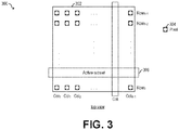
Figure 3 shows a diagram illustrating a top view of a layout of a possible implementation of a pixel array of a DTOF image sensor (not to scale), according to an embodiment of the present invention; -
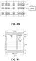
Figures 4A-4C show different levels of detail of a possible implementation of a subset of pixels of the pixel array ofFigure 3 , according to an embodiment of the present invention; -
Figure 5 shows a column of pixels of the pixel array ofFigure 3 , according to an embodiment of the present invention; -
Figures 6A-6C show different levels of detail of a possible implementation of a subset of pixels of the pixel array ofFigure 3 , according to an embodiment of the present invention; and -
Figure 7 shows a column of pixels of the pixel array ofFigure 3 , according to an embodiment of the present invention. - Corresponding numerals and symbols in different figures generally refer to corresponding parts unless otherwise indicated. The figures are drawn to clearly illustrate the relevant aspects of the preferred embodiments and are not necessarily drawn to scale.
- The making and using of the embodiments disclosed are discussed in detail below. It should be appreciated, however, that the present invention provides many applicable inventive concepts that can be embodied in a wide variety of specific contexts. The specific embodiments discussed are merely illustrative of specific ways to make and use the invention, and do not limit the scope of the invention.
- The description below illustrates the various specific details to provide an in-depth understanding of several example embodiments according to the description. The embodiments may be obtained without one or more of the specific details, or with other methods, components, materials and the like. In other cases, known structures, materials or operations are not shown or described in detail so as not to obscure the different aspects of the embodiments. References to "an embodiment" in this description indicate that a particular configuration, structure or feature described in relation to the embodiment is included in at least one embodiment. Consequently, phrases such as "in one embodiment" that may appear at different points of the present description do not necessarily refer exactly to the same embodiment. Furthermore, specific formations, structures or features may be combined in any appropriate manner in one or more embodiments.
- Embodiments of the present invention will be described in a specific context, routing for (e.g., high density) DTOF image sensors. Embodiments of the present invention may be used in other types of sensors, such as other types of SPAD-based image sensors, as well as non-SPAD based sensors, such as a CMOS sensor (where, e.g., the SPAD is replaced by a CMOS sensor, and logic and tri-state buffering is replaced, e.g., by a source-follower-based readout circuit, for example).
- DTOF image sensors are generally data-heavy, with many signals to be routed. For example, the routing between
SPADs 202 and TDC 206 may include metal traces formed, e.g., in the metal layers of the IC that includesSPAD array 104 andTDCs 102. For example, each SPAD or group ofSPADs 202 may be connected with a tri-stated buffer to a full height column line connected to TDC 206. - Some of the signals, such as signals between
SPADs 202 and TDC 206, are sensitive to timing. For such signals, it may be desirable to maintain timing precision across the routing as well as over process, voltage, and temperature (PVT) variations. Some of the signals, such as the signals between TDC 206 andprocessor 110, carry high frequency data, thereby impacting power consumption. In a high resolution DTOF sensor (e.g., with hundreds or thousands of SPADs, or more), routing the DTOF sensor signals may be challenging. - Some embodiments advantageously reduce the number of routes and/or the length of the routes in a DTOF image sensor, e.g., to improve timing precision, and/or reduce power consumption, and/or reduce area, and/or achieve higher density of pixels, and/or achieve higher resolution, for example.
-
Figure 3 shows a diagram illustrating a top view of a layout of a possible implementation ofpixel array 302 of DTOF image sensor 300 (not to scale), according to an embodiment of the present invention.Pixel array 302 includes M columns and N rows ofpixels 304. Eachpixel 304 includes 1 or more SPADs.Pixel array 302 includes a plurality of subset of pixels 304 (only 1 subset of pixels, active subset ofpixels 306, is shown inFigure 3 for clarity purposes). - During normal operation, different subsets of pixels are activated sequentially to sense light to allow for ToF determinations. For example,
Figure 3 shows active subset ofpixels 306.Pixels 304 inside active subset ofpixels 306 are active whilepixels 304 outside active subset ofpixels 306 are inactive. It is understood thatactive subset 306 represents the subset ofpixels 304 that is currently active, and that the location ofactive subset 306 may dynamically change (e.g., sequentially in the vertical direction over each subset of pixels) during the integration process. -
Pixels 304 inside active subset of pixels 306 (also referred to as active pixels) sense reflectedlight pulses 114. Corresponding TDC(s) (not shown inFigure 3 ) sense events produced by theactive pixels 304 when theactive pixels 304 are excited by light. The TDC(s) then generate corresponding timestamps (based on the received events) that are then used to generate ToF histograms in a known manner. The process of sensing light byactive pixels 304, and the generation of corresponding timestamps and ToF histograms may be referred to as an integration process. - Once the integration process is complete (e.g., over all subset of pixels of pixel array 302), data associated with pixels 304 (e.g., the corresponding timestamps or ToF histograms) are read (e.g., by processor 110) in a data readout process.
- In some embodiments, M and N may be greater than 100, such as 120, 210, or 360 for example. Other values for M and N, such as higher than 360 or lower than 100 may also be used. In some embodiments M may be different than N.
- In some embodiments, each subset of pixels of pixel array 302 (e.g., such as active subset of pixels 306) may have M columns and N/k rows, where k is a positive integer greater than or equal to 1. In some embodiments, each subset of pixels may have less than M columns, such as M/2, M/3, or a different number, for example.
- As a non-limiting example, in an embodiment, N is equal to 360, M is equal to 120, and k is equal to 12. In such embodiment, each subset of pixels includes 30 pixels per column, and 120 columns of
pixels 304. - During the integration process of such embodiment, events generated by
active pixels 304 in each column Coli of active subset of pixels 306 (3600 active pixels divided into 120 columns in this example) may be processed by dedicated TDC(s) and histogram generation circuits (not shown). Onceactive pixels 304 inside subset ofpixels 306 finish the integration process, such active pixels become inactive and the next subset of pixels (such as a subset of pixels immediately below subset of pixels 306) becomes active. - Once all subsets of
pixels 304 ofpixel array 302 have been (e.g., sequentially) activated during the integration process, data associated with each pixel 304 (e.g., the corresponding timestamps or ToF histograms) is read in the data readout process. - In some embodiments, array of
pixels 302 is implemented in a single monolithic substrate inside an IC. In some embodiments, the single monolithic substrate may also include the TDCs, histogram generation circuits, and illumination source. In some embodiments,processor 110, or portions ofprocessor 110 may also be integrated inside the IC. - In an embodiment of the present invention, routing inside a DTOF sensor is reduced by disposing TDCs above and below a subset of SPADs. A split bus routes half of the SPADs of the subset of SPADs to corresponding top TDCs and the other half of the SPADs to corresponding bottom TDCs. In some embodiments, the split bus advantageously allows for twice more SPADs to be routed when compared to implementations that route each column of SPADs to TDCs in a single location (e.g., all TDCs above the subset of SPADs or all TDCs below the subset of SPADs).
-
Figures 4A-4C show different levels of detail of column Coli of subset ofpixels 400, according to an embodiment of the present invention. Each subset of pixels of pixel array 302 (such as active subset of pixels 306) maybe implemented as subset ofpixels 400. It is understood that column Coli could be any column of the M columns ofpixel array 302. - As shown in
Figure 4A , column Coli of subset ofpixels 400 includes a plurality ofpixels 304 coupled to respectivebus driving circuits 415. Each pixel includes SPAD front-end circuit 410,SPAD 412, and buffer 414. Eachbus driving circuit 415 includes a plurality of bus drivers (416 or 424) coupled to routingbus 402. As shown inFigure 4A , routingbus 402 is coupled to a top plurality ofTDCs 404 and to a bottom plurality ofTDCs 406. Each bus driver (416 or 424) may route a signal received up to the respective TDC of the top plurality ofTDCs 404 or down to the respective TDC of the bottom plurality ofTDCs 406. - Even though
Figure 4A shows eachpixel 304 including asingle SPAD 412 coupled to buffer 414, it us understood that some embodiments may replacesingle SPAD 412 and buffer 414 with a plurality of SPADs (such as SPADs 202) coupled to an OR tree. - As shown in
Figures 4A and4B , eachSPAD 412 is coupled to at least onebus driver circuit 416. -
Bus driver 416 is configured to propagate the signal at the output of buffer 414 up (via buffer 420) or down (via buffer 422) routingbus 402, e.g., when select signal Sel is equal to 1. When select signal Sel is equal to, e.g., 0, signal S420 is buffered by multiplexer (MUX) 418 into the input ofbuffer 422, which propagates it down viabuffer 422. When select signal Sel is equal to, e.g., 2, signal S422 is buffered byMUX 418 into the input ofbuffer 420, which propagates it up viabuffer 420. In other words, when select signal Sel is equal to, e.g., 1,bus driver 416 propagates the signal from the corresponding SPAD 412 (up or down), e.g., depending on the location of the SPAD with respect to the subset ofpixels 400. And when select signal Sel is equal to, e.g., 0 or 1,bus driver 416 behaves as a buffer that buffers up (e.g., when Sel = 2) or down (e.g., when Sel = 0) the signals coming from routingbus 402. -
Buffers buffers -
Bus driver 424 is configured to propagate signals from routingbus 402 either up or down. As shown,bus drivers 424 are capable of dynamically reconfiguring the direction of buffering. In some embodiments,bus driver 424 may be implemented asbus driver 416. -
Controller 450 is configured to generate select signals Sel for each ofbus drivers pixels 400 to configure them as up-buffers (e.g., Sel = 2), down-buffers (e.g., Sel = 0), or for buffering event signals of their respective SPADs (e.g., Sel = 0). - Some embodiments include one
controller 450 per subset ofpixels 400. Other embodiments include asingle controller 450 for all subset of pixels ofpixel array 302. Other implementations are also possible. -
Controller 450 may be implemented, for example, using combinatorial logic (such as a finite state machine, for example), e.g., coupled to a memory (such as registers, OTP, ROM, or RAM, for example). - In some embodiments, routing
bus 402 includes L/2 routing lines when column Coli of subset ofpixels 400 includesL pixels 304. For example, when column Coli of subset ofpixels 400 has 30pixels 304, routingbus 402 has 15 routing lines (which are respectively coupled to 15TDCs 404 and 15 TDCs 406). In some embodiments, L maybe higher than 30, such as 40, or higher, or lower than 30, such as 20 or lower. - As shown in
Figure 4B , each routing line ofrouting bus 402 is shared by twopixels 304 of column Coli of subset ofpixels 400 to propagate signals associated with their respective SPADs (as illustrated by the presence bus driver 416). -
Figure 4C shows a top view ofpixel array 302 column Coli ofpixel array 302 showing the physical placement ofpixels 304, routingbus 402 and correspondingbus driver circuits 415, and top and bottom TDCs 404 and 406, respectively, according to an embodiment of the present invention. - During normal operation, when subset of
pixels 400 is active,controller 450 configuresbus drivers pixel 304 propagates event signals associated with theirrespective SPADs 412 usingbus driver 416. The top half ofpixels 304 propagate their respective event signals up totop TDCs 404 via thebus drivers 424 coupled between therespective bus driver 416 andtop TDCs 404. The bottom half of pixels propagate their respective event signals down tobottom TDCs 406 via thebus drivers 424 between therespective bus driver 416 andbottom TDCs 406. - During normal operation, subset of pixels that are below the active subset of pixels operate their
bus drivers routing bus 402 tobottom TDCs 406. In a similar manner, subset of pixels that are above the active subset of pixels operate theirbus drivers routing bus 402 totop TDCs 404. - In some embodiments, using
bus drivers 424 advantageously allows for preserving timing precision of the event signals generated bySPADs 412. In some embodiments, additional buffers and/or inverters may be used to balance the event signals fromSPADs 412. - In some embodiments, the placement of
bus drivers 416 with respect to the location ofpixel 304 in subset ofpixels 400 may be selected to balance timing. For example, in some embodiments, thepixel 304 closest to the top of subset of pixel 400 (and the one closest to the bottom) has its correspondingbus driver 416 farthest to the right, while the pair ofpixel 304 closest to the center of subset ofpixels 400 have theircorresponding bus driver 416 closest to the left, e.g., to compensate for the longer routing of the pixels closest to the center of subset ofpixels 400 when compared to those at the edge of subset ofpixels 400. - SPAD front-
end circuit 410 is configured to biasSPAD 412. In some embodiments, SPAD front-end circuit has an enable input configured to receive a spad_enable signal (not shown). In such embodiments, SPAD front-end circuit may enableSPAD 412 when the spad_enable signal is asserted. In some embodiments, activating a SPAD includes asserting the spad_enable signal. In some embodiments, activating a subset of SPAD includes asserting the spad_enable signal of each SPAD in the subset of SPADs. SPAD front-end circuit 410 maybe implemented in any way known in the art. - As shown in
Figures 4A-4C , some embodiments includetop TDCs 404 at the top of column Coli, andbottom TDCs 406 at the bottom of column Coli. Some embodiments may have additional rows of TDCs embedded inpixel array 302. For example,Figure 5 shows a column Coli ofpixel array 302, according to an embodiment of the present invention. - The embodiment of
Figure 5 operates in a similar manner as the embodiment illustrated inFigures 4A-4C . The embodiment ofFigure 5 , however, includes two splitrouting buses 402 in a column Coli ofpixels 304. In such embodiments, two active subset ofpixels 500 may perform the integration process simultaneously. Some embodiments may include more than two splitrouting buses 402. - In an embodiment of the present invention, routing inside a DTOF sensor is reduced by sharing a bus for routing SPAD events (e.g., SPAD pulses) from each subset of SPADs to corresponding, in-array, TDCs and histogram generation circuits, and for data readout.
-
Figures 6A-6C show different levels of detail of column Coli of subset ofpixels 600, according to an embodiment of the present invention. Each subset of pixels of pixel array 302 (such as active subset of pixels 306) may be implemented as subset ofpixels 600. It is understood that column Coli could be any column of the M columns ofpixel array 302. - As shown in
Figure 6A , column Coli of subset ofpixels 600 includes a plurality ofpixels 304 coupled to routingbus 620 via respectivebus driving circuits 602. As shown inFigure 6B , Routingbus 620 has J routing lines, where J is a positive integer greater than or equal to 1. Routingline 620j could be any of the J routing lines ofrouting bus 620. - Each
pixel 304 includes SPAD front-end circuit 410,SPAD 412, and buffer 414. Eachbus driving circuit 602 includesMUX 604 andtri-state buffer 606 coupled to arouting line 620j ofrouting bus 620. As shown inFigure 6A , routingline 620j is coupled to a plurality of time-capture circuits 608, where each time-capture circuit 608 includesTDC 610 andhistogram generation circuit 612. - The plurality of time-
capture circuits 608 are shared across all subset of pixels of column Colj, and each column of pixels has its corresponding plurality of time-capture circuits 608. - During the integration process of subset of pixels 600 (when subset of
pixels 600 is active and in integration mode) read_histogram signal is deasserted (e.g., logic low), buffer_enable signal is asserted (e.g., logic high) and spad_enable signal is asserted (e.g., logic_high), and section_enable signal is deasserted (e.g., logic low). During this state, routingline 620j is configured to propagate event signals generated bySPAD 412 via buffer 414,MUX 604, andtri-state buffer 606 intorouting line 620j.TDC 610 receives the generated event signals from routingline 620j andhistogram generation circuit 612 generates ToF histograms based on the output ofTDC 610. Sincetri-state buffers 614 are disabled, eachpixel 304 that is coupled to routingline 620j is isolated from each other so that eachpixel 304 may perform the integration operation in cooperation with the corresponding time-capture circuit 608. - During the readout process (when subset of
pixels 600 is in readout mode), read_histogram signal is asserted (e.g., logic high), spad_enable signal is deasserted (e.g., logic_low), and section_enable signal is asserted (e.g., logic high). During this state, buffer_enable signal is sequentially asserted (e.g., logic high) so that data from each histogram generation circuit 612 (e.g., ToF histogram data, such as counts per bin) are sequentially propagated via an array bus (e.g., where the array bus includes the (e.g., vertical) routing lines connectingtri-state buffers MUX 604, and then totri-state buffer 606 intorouting line 620j.Processor 110 then sequentially receives the data from eachhistogram generation circuit 612 and, e.g., may perform further processing. - In some embodiments, the J (e.g., vertical) routing lines of
routing bus 620 repeat in a (e.g., vertical) pattern. For example, if subset ofpixels 600 has 30pixels 304 per column, and J is 10, then there are 3 pixels coupled to each routing line ofrouting bus 620 per subset ofpixels 600. The pattern repeats for each subset of pixels of column Coli. - In such example, there are 30 TDCs 610 (and corresponding histogram generation circuits) associated to column Coli and coupled to the routing bus 620 (3 TDCs coupled to each of the 10 routing lines of routing bus 620).
- As shown in
Figure 6C , each column Coli includes a column ofpixels 304 and a column of time-capture circuits 608. In some embodiments,pixels array 302 includes M columns ofpixels 304 alternating with M columns of time-capture circuits 608, wherein M is a positive integer greater than 1. Other arrangements are also possible. For example, in some embodiments,pixel array 302 includes M/2 pairs of columns ofpixels 304 alternating with M/2 pairs of columns of time-capture circuits 608 (e.g., in a mirror image arrangement). -
Controller 650 is configured to generate read_histogram, buffer_enable, spad_enable, and section_enable signals to configure subset ofpixels 600, e.g., for integration or for readout. - Some embodiments include one
controller 650 per subset ofpixels 600. Other embodiments include asingle controller 650 for all subset of pixels ofpixel array 302. Other implementations are also possible. -
Controller 650 may be implemented, for example, using combinatorial logic (such as a finite state machine, for example), e.g., coupled to a memory (such as registers, OTP, ROM, or RAM, for example). - Advantages of some embodiments include allowing the reduction of routing by sharing the routing bus to route SPAD pulses during the integration process and to route histogram data during data readout. In some embodiments, the reduction in routing may allow for the implementation of higher resolution DTOF sensors since, e.g., the complexities of routing congestion associated with coupling routing lines to histogram generation circuits that may be substantially larger than a pixel (e.g., may be spread over the height of multiple pixels) maybe mitigated or avoided. Some embodiments may advantageously achieve a very compact implementation since there is no additional area for histogram generation circuits outside the array.
-
Figure 7 shows a column Coli ofpixel array 302, according to an embodiment of the present invention. The embodiment ofFigure 7 operates in a similar manner as the embodiment illustrated inFigures 6A-6C . The embodiment ofFigure 7 , however, includesbuffer 704 for buffering histogram data directly intorouting line 620j instead of going throughbus driving circuit 602. - Example embodiments of the present invention are summarized here. Other embodiments can also be understood from the entirety of the specification and the claims filed herein.
- Example 1. A time-of-flight (ToF) sensor including: an array of pixels arranged in rows and columns, the array of pixels including first and second subsets of pixels, each pixel of the array of pixels configured to generate event signals; a first plurality of time to digital converters (TDCs); a second plurality of TDCs; a first routing bus coupled to the first and second pluralities of TDCs and to the first and second subsets of pixels, the first routing bus including a first plurality of bus drivers associated with the first subset of pixels and a second plurality of bus drivers associated with the second subset of pixels, the first plurality of bus drivers coupled to the second plurality of TDCs via the second plurality of bus drivers, and the second plurality of bus drivers coupled to the first plurality of TDCs via the first plurality of bus drivers; and a controller configured to: when the first subset of pixels is active and the second subset of pixels is not active, control the first plurality of bus drivers to route event signals from half of the pixels of the first subset of pixels to the first plurality of TDCs and control the first and second plurality of bus drivers to route event signals from the other half of the pixels of the first subset of pixels to the second plurality of TDCs, and when the first subset of pixels is not active and the second subset of pixels is active, control the first plurality of bus drivers to route event signals from the second subset of pixels to the first plurality of TDCs.
- Example 2. The ToF sensor of example 1, where: the first subset of pixels includes L pixels, L being a positive integer greater than 1; the second subset of pixels includes L pixels; and the first routing bus includes L/2 routing lines.
- Example 3. The ToF sensor of one of examples 1 or 2, where L is 30.
- Example 4. The ToF sensor of one of examples 1 to 3, where each routing line of the first routing bus is configured to receive event signals from two pixels of the first subset of pixels.
- Example 5. The ToF sensor of one of examples 1 to 4, where the first and second subsets of pixels are physically disposed between the first and second pluralities of TDCs.
- Example 6. The ToF sensor of one of examples 1 to 5, where each pixel of the first subset of pixels includes a single photon avalanche diode (SPAD) coupled to a respective bus driver of the first plurality of bus drivers.
- Example 7. The ToF sensor of one of examples 1 to 6, where each bus driver of the first plurality of bus drivers includes: a multiplexer; a first buffer having an input coupled to an output of the multiplexer and an output coupled to a first input of the multiplexer; and a second buffer having an input coupled to the output of the multiplexer and an output coupled to a second input of the multiplexer.
- Example 8. The ToF sensor of one of examples 1 to 7, where the first and second subset of pixels correspond to a first column of pixels of the array of pixels, the ToF sensor further including: a second routing bus associated with a second column of pixels of the array of pixels, where the second column of pixels includes a third subset of pixels; and third and fourth pluralities of TDCs, where, when the third subset of pixels is active, the second routing bus is configured to route event signals from half of the pixels of the third subset of pixels to the third plurality of TDCs and to route event signals from the other half of the pixels of the third subset of pixels to the fourth plurality of TDCs.
- Example 9. The ToF sensor of one of examples 1 to 8, where the first and third subset of pixels are configured to be active at the same time.
- Example 10. The ToF sensor of one of examples 1 to 9, further including an illumination source configured to generate light pulses, where pixels of the array of pixels are configured to generate event signals from light pulses that are based on the generated light pulses.
- Example 11. The ToF sensor of one of examples 1 to 10, further including a processor configured to generate ToF histograms based on outputs of the first and second pluralities of TDCs.
- Example 12. A method including: activating a first subset of pixels of an array of pixels of a time-of-flight (ToF) sensor, the array of pixels being arranged in rows and columns; when the first subset of pixels is active, controlling a first plurality of bus drivers of a first routing bus to route event signals from half of the pixels of the first subset of pixels to a first plurality of TDCs and controlling the first plurality of bus drivers and a second plurality of bus drivers to route event signals from the other half of the pixels of the first subset of pixels to a second plurality of TDCs, where the first plurality of bus drivers is coupled to the second plurality of TDCs via the second plurality of bus drivers, where the second plurality of bus drivers is coupled to the first plurality of TDCs via the first plurality of bus drivers, where the first plurality of bus drivers is associated with the first subset of pixels, and where the second plurality of bus drivers associated with a second subset of pixels of the array of pixels; activating the second subset of pixels; and when the second subset of pixels is active, controlling the first plurality of bus drivers to route event signals from the second subset of pixels to the first plurality of TDCs.
- Example 13. The method of example 12, further including receiving event signals with a routing line of the first routing bus from two pixels of the first subset of pixels.
- Example 14. The method of one of examples 12 or 13, further including: generating a plurality of light pulses; and receiving reflected light pulses with the array of pixels, where the event signals from the pixels of the first subset of pixels are based on the reflected light pulses.
- Example 15. The method of one of examples 12 to 14, further including generating ToF histograms based on outputs from the first and second pluralities of TDCs.
- Example 16. The method of one of examples 12 to 15, where: the first subset of pixels includes L pixels, L being a positive integer greater than 1; the second subset of pixels includes L pixels; and the first routing bus includes L/2 routing lines.
- Example 17. An integrated circuit (IC) including: an array of pixels arranged in rows and columns, the array of pixels including a first subset of pixels, each pixel of the array of pixels configured to generate event signals; a top plurality of time to digital converters (TDCs) physically disposed at the top of the array of pixels; a bottom plurality of TDCs physically disposed at the bottom of the array of pixels; a routing bus coupled to the top and bottom pluralities of TDCs and to the first subset of pixels, the routing bus including a plurality of bus drivers associated with the first subset of pixels; and a controller configured to: when the first subset of pixels is active, control the plurality of bus drivers to route event signals from a top half of the pixels of the first subset of pixels to the top plurality of TDCs and to route event signals from a bottom half of the pixels of the first subset of pixels to the bottom plurality of TDCs, and when the first subset of pixels is not active, control all of the plurality of bus drivers to route event signals of the routing bus to the top plurality of TDCs.
- Example 18. The IC of example 17, where each routing line of the routing bus is configured to receive event signals from two pixels of the first subset of pixels.
- Example 19. The IC of one of examples 17 or 18, where: the first subset of pixels includes L pixels, L being a positive integer greater than 1; and the routing bus includes L/2 routing lines.
- Example 20. The IC of one of examples 17 to 19, where each bus driver of the plurality of bus drivers includes: a multiplexer; a first buffer having an input coupled to an output of the multiplexer and an output coupled to a first input of the multiplexer, the output of the first buffer further coupled to a top TDC of the top plurality of TDCs; and a second buffer having an input coupled to the output of the multiplexer and an output coupled to a second input of the multiplexer, the output of the second buffer further coupled to a bottom TDC of the plurality of bottom TDCs.
- Example 21. A time-of-flight (ToF) sensor including: an array of pixels arranged in rows and columns, each pixel of the array of pixels configured to generate event signals, the array of pixels including a subset of pixels; a routing bus coupled to the subset of pixels; a plurality of time-capture circuits coupled to the routing bus; and a controller configured to: when the subset of pixels is in integration mode, route event signals from a first pixel of the subset of pixels to a first time-capture circuit of the plurality of time-capture circuits via a first routing line of the routing bus, and when the subset of pixels is in readout mode, route data from the first time-capture circuit to a reading circuit via the first routing line.
- Example 22. The ToF sensor of example 21, where the first routing line includes a section tri-state buffer coupled between the first pixel and a second pixel of the subset of pixels, and where the controller is further configured to: when the subset of pixels is in integration mode, disable the section tri-state buffer; and when the subset of pixels is in readout mode, enable the section tri-state buffer.
- Example 23. The ToF Sensor of one of examples 21 or 22, where the controller is further configured to, when the subset of pixels is in integration mode, route event signals from the second pixel to a second time-capture circuit of the plurality of time-capture circuits via the first routing line.
- Example 24. The ToF sensor of one of examples 21 to 23, where the first time-capture circuit includes a time-to-digital converter (TDC).
- Example 25. The ToF sensor of one of examples 21 to 24, where the first time-capture circuit further includes a histogram generation circuit, and where routing data from the first time-capture circuit to the reading circuit includes routing ToF histograms.
- Example 26. The ToF sensor of one of examples 21 to 25, where each time-capture circuit of the plurality of time-capture circuits includes a respective tri-state buffer coupled to the routing bus.
- Example 27. The ToF sensor of one of examples 21 to 26, where each pixel of the subset of pixels includes a single photon avalanche diode (SPAD) coupled to the routing bus via a respective bus driving circuit.
- Example 28. The ToF sensor of one of examples 21 to 27, where each bus driving circuit includes a tri-state buffer coupled to the routing bus.
- Example 29. The ToF sensor of one of examples 21 to 28, where each bus driving circuit further includes a multiplexer having a first input coupled to the respective SPAD, a second input coupled to a corresponding time-capture circuit of the plurality of time-capture circuits, and an output coupled to the respective tri-state buffer.
- Example 30. The ToF sensor of one of examples 21 to 29, where the subset of pixels correspond to a first column of pixels of the array of pixels, the ToF sensor further including: a second routing bus associated with a second column of pixels of the array of pixels, where the second column of pixels includes a second subset of pixels; and a second plurality of time-capture circuits coupled to the second routing bus, where, when the second subset of pixels is in integration mode, a second routing line of the second routing bus is configured to route event signals from a second pixel of the second subset of pixels to a second time-capture circuit of the second plurality of time-capture circuits, and when the second subset of pixels is in readout mode, the second routing line is configured to route data from the second time-capture circuit to the reading circuit.
- Example 31. The ToF sensor of one of examples 21 to 30, where the subset of pixels and the second subset of pixels are configured to be in integration mode at the same time.
- Example 32. The ToF sensor of one of examples 21 to 31, where the reading circuit includes an external processor.
- Example 33. The ToF sensor of one of examples 21 to 32, further including an illumination source configured to generate light pulses, where pixels of the array of pixels are configured to generate event signals from light pulses that are based on the generated light pulses.
- Example 34. A method including: setting a subset of pixels of an array of pixels of a time-of-flight (ToF) sensor to integration mode, the array of pixels being arranged in rows and columns; when the subset of pixels is in integration mode, routing event signals from a first pixel of the subset of pixels to a first time-capture circuit of a plurality of time-capture circuits via a first routing line of a routing bus; setting the subset of pixels to readout mode; and when the subset of pixels is in readout mode, routing data from the first time-capture circuit to a reading circuit via the first routing line.
- Example 35. The method of example 34, further including: when the subset of pixels is in integration mode, disabling a section tri-state buffer that is coupled between the first pixel and a second pixel of the subset of pixels; and when the subset of pixels is in readout mode, enabling the section tri-state buffer.
- Example 36. The method of one of examples 34 or 35, further including, when the subset of pixels is in integration mode, routing event signals from the second pixel to a second time-capture circuit of the plurality of time-capture circuits via the first routing line.
- Example 37. The method of one of examples 34 to 36, further including: generating a plurality of light pulses; and receiving reflected light pulses with the array of pixels, where the event signals are based on the reflected light pulses.
- Example 38. An integrated circuit (IC) including: an array of pixels arranged in rows and columns, each pixel of the array of pixels configured to generate event signals, the array of pixels including a subset of pixels; a routing bus coupled to the subset of pixels, the routing bus including J routing lines, where J is a positive integer greater than 1, where each routing line of the J routing lines is coupled to more than 1 pixels of the subset of pixels; a plurality of time-capture circuits coupled to the routing bus; and a controller configured to: when the subset of pixels is in integration mode, route event signals from a first pixel of the subset of pixels to a first time-capture circuit of the plurality of time-capture circuits via a first routing line of the routing bus, and when the subset of pixels is in readout mode, route data from the first time-capture circuit to a reading circuit via the first routing line.
- Example 39. The IC of example 38, where each routing line of the J routing lines is coupled to 3 pixels of the subset of pixels.
- Example 40. The IC of one of examples 38 or 39, where the array of pixels includes M columns of pixels and M columns of TDCs in an alternate pattern, where M is a positive integer greater than 1.
- While this invention has been described with reference to illustrative embodiments, this description is not intended to be construed in a limiting sense. Various modifications and combinations of the illustrative embodiments, as well as other embodiments of the invention, will be apparent to persons skilled in the art upon reference to the description. It is therefore intended that the appended claims encompass any such modifications or embodiments.
Claims (15)
- A time-of-flight (ToF) sensor comprising:an array of pixels arranged in rows and columns, the array of pixels comprising first and second subsets of pixels, each pixel of the array of pixels configured to generate event signals;a first plurality of time to digital converters (TDCs);a second plurality of TDCs;a first routing bus coupled to the first and second pluralities of TDCs and to the first and second subsets of pixels, the first routing bus comprising a first plurality of bus drivers associated with the first subset of pixels and a second plurality of bus drivers associated with the second subset of pixels, the first plurality of bus drivers coupled to the second plurality of TDCs via the second plurality of bus drivers, and the second plurality of bus drivers coupled to the first plurality of TDCs via the first plurality of bus drivers; anda controller configured to:when the first subset of pixels is active and the second subset of pixels is not active, control the first plurality of bus drivers to route event signals from half of the pixels of the first subset of pixels to the first plurality of TDCs and control the first and second plurality of bus drivers to route event signals from the other half of the pixels of the first subset of pixels to the second plurality of TDCs, andwhen the first subset of pixels is not active and the second subset of pixels is active, control the first plurality of bus drivers to route event signals from the second subset of pixels to the first plurality of TDCs.
- The ToF sensor of claim 1, wherein each routing line of the first routing bus is configured to receive event signals from two pixels of the first subset of pixels.
- The ToF sensor of claim 1 or 2, wherein the first and second subsets of pixels are physically disposed between the first and second pluralities of TDCs.
- The ToF sensor of any of claims 1 to 3, wherein each pixel of the first subset of pixels comprises a single photon avalanche diode (SPAD) coupled to a respective bus driver of the first plurality of bus drivers.
- The ToF sensor of any of claims 1 to 4, wherein each bus driver of the first plurality of bus drivers comprises:a multiplexer;a first buffer having an input coupled to an output of the multiplexer and an output coupled to a first input of the multiplexer; anda second buffer having an input coupled to the output of the multiplexer and an output coupled to a second input of the multiplexer.
- The ToF sensor of any of claims 1 to 5, wherein the first and second subset of pixels correspond to a first column of pixels of the array of pixels, the ToF sensor further comprising:a second routing bus associated with a second column of pixels of the array of pixels, wherein the second column of pixels comprises a third subset of pixels; andthird and fourth pluralities of TDCs, wherein, when the third subset of pixels is active, the second routing bus is configured to route event signals from half of the pixels of the third subset of pixels to the third plurality of TDCs and to route event signals from the other half of the pixels of the third subset of pixels to the fourth plurality of TDCs.
- The ToF sensor of claim 6, wherein the first and third subset of pixels are configured to be active at the same time.
- The ToF sensor of any of claims 1 to 7, further comprising an illumination source configured to generate light pulses, wherein pixels of the array of pixels are configured to generate event signals from light pulses that are based on the generated light pulses, and, optionally, the ToF sensor further comprising a processor configured to generate ToF histograms based on outputs of the first and second pluralities of TDCs.
- A method comprising:activating a first subset of pixels of an array of pixels of a time-of-flight (ToF) sensor, the array of pixels being arranged in rows and columns;when the first subset of pixels is active, controlling a first plurality of bus drivers of a first routing bus to route event signals from half of the pixels of the first subset of pixels to a first plurality of TDCs and controlling the first plurality of bus drivers and a second plurality of bus drivers to route event signals from the other half of the pixels of the first subset of pixels to a second plurality of TDCs, wherein the first plurality of bus drivers is coupled to the second plurality of TDCs via the second plurality of bus drivers, wherein the second plurality of bus drivers is coupled to the first plurality of TDCs via the first plurality of bus drivers, wherein the first plurality of bus drivers is associated with the first subset of pixels, and wherein the second plurality of bus drivers associated with a second subset of pixels of the array of pixels;activating the second subset of pixels; andwhen the second subset of pixels is active, controlling the first plurality of bus drivers to route event signals from the second subset of pixels to the first plurality of TDCs.
- The method of claim 9, further comprising receiving event signals with a routing line of the first routing bus from two pixels of the first subset of pixels.
- The method of claim 9 or 10, further comprising:generating a plurality of light pulses; andreceiving reflected light pulses with the array of pixels, wherein the event signals from the pixels of the first subset of pixels are based on the reflected light pulses, and optionallygenerating ToF histograms based on outputs from the first and second pluralities of TDCs.
- The method of any of claims 9 to 11 or the TOF sensor of any of claims 1 to 8, wherein:the first subset of pixels comprises L pixels, L being a positive integer greater than 1;the second subset of pixels comprises L pixels; andthe first routing bus comprises L/2 routing lines;and wherein L is for example 30.
- An integrated circuit (IC) comprising:an array of pixels arranged in rows and columns, each pixel of the array of pixels configured to generate event signals, the array of pixels comprising a subset of pixels;a routing bus coupled to the subset of pixels, the routing bus comprising J routing lines, wherein J is a positive integer greater than 1, wherein each routing line of the J routing lines is coupled to more than 1 pixels of the subset of pixels;a plurality of time-capture circuits coupled to the routing bus; anda controller configured to:when the subset of pixels is in integration mode, route event signals from a first pixel of the subset of pixels to a first time-capture circuit of the plurality of time-capture circuits via a first routing line of the routing bus, andwhen the subset of pixels is in readout mode, route data from the first time-capture circuit to a reading circuit via the first routing line.
- The IC of claim 13, wherein each routing line of the J routing lines is coupled to 3 pixels of the subset of pixels.
- The IC of claim 13 or 14, wherein the array of pixels comprises M columns of pixels and M columns of TDCs in an alternate pattern, wherein M is a positive integer greater than 1.
Priority Applications (1)
| Application Number | Priority Date | Filing Date | Title |
|---|---|---|---|
| EP23182908.6A EP4254000B1 (en) | 2020-06-08 | 2021-05-26 | Routing for dtof sensors |
Applications Claiming Priority (1)
| Application Number | Priority Date | Filing Date | Title |
|---|---|---|---|
| US16/895,477 US11428792B2 (en) | 2020-06-08 | 2020-06-08 | Routing for DTOF sensors |
Related Child Applications (2)
| Application Number | Title | Priority Date | Filing Date |
|---|---|---|---|
| EP23182908.6A Division EP4254000B1 (en) | 2020-06-08 | 2021-05-26 | Routing for dtof sensors |
| EP23182908.6A Division-Into EP4254000B1 (en) | 2020-06-08 | 2021-05-26 | Routing for dtof sensors |
Publications (2)
| Publication Number | Publication Date |
|---|---|
| EP3923025A1 true EP3923025A1 (en) | 2021-12-15 |
| EP3923025B1 EP3923025B1 (en) | 2023-10-11 |
Family
ID=76159235
Family Applications (2)
| Application Number | Title | Priority Date | Filing Date |
|---|---|---|---|
| EP23182908.6A Active EP4254000B1 (en) | 2020-06-08 | 2021-05-26 | Routing for dtof sensors |
| EP21175855.2A Active EP3923025B1 (en) | 2020-06-08 | 2021-05-26 | Routing for dtof sensors |
Family Applications Before (1)
| Application Number | Title | Priority Date | Filing Date |
|---|---|---|---|
| EP23182908.6A Active EP4254000B1 (en) | 2020-06-08 | 2021-05-26 | Routing for dtof sensors |
Country Status (3)
| Country | Link |
|---|---|
| US (2) | US11428792B2 (en) |
| EP (2) | EP4254000B1 (en) |
| CN (2) | CN113840105B (en) |
Families Citing this family (2)
| Publication number | Priority date | Publication date | Assignee | Title |
|---|---|---|---|---|
| US10818721B2 (en) * | 2018-08-22 | 2020-10-27 | Stmicroelectronics (Research & Development) Limited | Pixel circuit and method of operating the same in an always-on mode |
| WO2022191773A1 (en) * | 2021-03-12 | 2022-09-15 | Ams Sensors Singapore Pte. Ltd. | Sensor device, sensor module, imaging system and method to operate a sensor device |
Citations (3)
| Publication number | Priority date | Publication date | Assignee | Title |
|---|---|---|---|---|
| US20170134710A1 (en) * | 2015-04-20 | 2017-05-11 | Samsung Electronics Co., Ltd. | Increasing tolerance of sensor-scanner misalignment of the 3d camera with epipolar line laser point scanning |
| US20180209846A1 (en) * | 2017-01-25 | 2018-07-26 | Apple Inc. | SPAD Detector Having Modulated Sensitivity |
| US20190018117A1 (en) * | 2017-07-11 | 2019-01-17 | Fondanzione Bruno Kessler | Optoelectronic sensor and method for measuring a distance |
Family Cites Families (11)
| Publication number | Priority date | Publication date | Assignee | Title |
|---|---|---|---|---|
| US6466265B1 (en) | 1998-06-22 | 2002-10-15 | Eastman Kodak Company | Parallel output architectures for CMOS active pixel sensors |
| US7465934B2 (en) | 2005-09-30 | 2008-12-16 | Eastman Kodak Company | Pixel array output routing structure for multi-channel CMOS imager sensors |
| US9013615B2 (en) | 2011-09-21 | 2015-04-21 | Semiconductor Components Industries, Llc | Image sensor with flexible interconnect capabilities |
| DE102014115310A1 (en) * | 2014-10-21 | 2016-04-21 | Infineon Technologies Ag | Image forming apparatus and a runtime image forming method |
| US20160290790A1 (en) * | 2015-03-31 | 2016-10-06 | Google Inc. | Method and apparatus for increasing the frame rate of a time of flight measurement |
| US9921298B2 (en) * | 2015-07-20 | 2018-03-20 | Google Llc | Method and apparatus for increasing the resolution of a time of flight pixel array |
| US10416293B2 (en) * | 2016-12-12 | 2019-09-17 | Sensl Technologies Ltd. | Histogram readout method and circuit for determining the time of flight of a photon |
| US10681295B2 (en) * | 2017-10-30 | 2020-06-09 | Omnivision Technologies, Inc. | Time of flight camera with photon correlation successive approximation |
| JP7290632B2 (en) * | 2018-05-24 | 2023-06-13 | ソニーセミコンダクタソリューションズ株式会社 | time measuring device |
| EP3814803A4 (en) * | 2018-08-16 | 2022-03-02 | Sense Photonics, Inc. | INTEGRATED LIDAR IMAGE SENSING DEVICES AND SYSTEMS AND RELATED METHODS OF OPERATION |
| KR20220136336A (en) * | 2020-02-10 | 2022-10-07 | 헤사이 테크놀로지 씨오., 엘티디. | Adaptive emitters and receivers for lidar systems |
-
2020
- 2020-06-08 US US16/895,477 patent/US11428792B2/en active Active
-
2021
- 2021-05-26 EP EP23182908.6A patent/EP4254000B1/en active Active
- 2021-05-26 EP EP21175855.2A patent/EP3923025B1/en active Active
- 2021-06-04 CN CN202110623662.4A patent/CN113840105B/en active Active
- 2021-06-04 CN CN202411324007.9A patent/CN118921572A/en active Pending
-
2022
- 2022-07-19 US US17/868,261 patent/US11822017B2/en active Active
Patent Citations (3)
| Publication number | Priority date | Publication date | Assignee | Title |
|---|---|---|---|---|
| US20170134710A1 (en) * | 2015-04-20 | 2017-05-11 | Samsung Electronics Co., Ltd. | Increasing tolerance of sensor-scanner misalignment of the 3d camera with epipolar line laser point scanning |
| US20180209846A1 (en) * | 2017-01-25 | 2018-07-26 | Apple Inc. | SPAD Detector Having Modulated Sensitivity |
| US20190018117A1 (en) * | 2017-07-11 | 2019-01-17 | Fondanzione Bruno Kessler | Optoelectronic sensor and method for measuring a distance |
Also Published As
| Publication number | Publication date |
|---|---|
| US11428792B2 (en) | 2022-08-30 |
| CN113840105A (en) | 2021-12-24 |
| CN118921572A (en) | 2024-11-08 |
| US11822017B2 (en) | 2023-11-21 |
| EP4254000B1 (en) | 2024-12-11 |
| CN113840105B (en) | 2024-10-15 |
| EP3923025B1 (en) | 2023-10-11 |
| EP4254000A3 (en) | 2023-11-15 |
| EP4254000A2 (en) | 2023-10-04 |
| US20220357435A1 (en) | 2022-11-10 |
| US20210382152A1 (en) | 2021-12-09 |
Similar Documents
| Publication | Publication Date | Title |
|---|---|---|
| US12345834B2 (en) | Time to digital converter | |
| US11822017B2 (en) | Routing for DTOF sensors | |
| US10444882B2 (en) | Touch sensing circuit, touch display device, and touch sensing method | |
| KR101648066B1 (en) | Analog to digital converter and image sensor including the same | |
| US11785356B2 (en) | Photoelectric conversion device with mask circuits | |
| US20090262229A1 (en) | Image sensor for high-speed data readout | |
| CN113221623B (en) | Readout IC | |
| US20150326242A1 (en) | Counter, analogue to digital converter including the counter and image sensing device including the analogue to digital converter | |
| CN210166496U (en) | Time measuring device | |
| CN103528691B (en) | The row strobe generation circuit of infrared focal plane array sensing circuit | |
| US7298405B2 (en) | Image sensing apparatus having photoelectric conversion elements and a scanning circuit | |
| US20230023133A1 (en) | Signal processing device and sensing module | |
| US20070132620A1 (en) | Array substrate and display device | |
| US7239260B2 (en) | Analog-to-digital interfacing device and method of analog-to-digital interfacing | |
| JP2024061597A (en) | Image sensor chip having depth information | |
| CN117255261A (en) | Image sensor and method of operating the same | |
| US8964059B2 (en) | Scanning circuit, solid-state image sensor, and camera | |
| JP7451649B2 (en) | Touch drive circuit and touch display device | |
| EP4496335A1 (en) | Image sensor and method of producing an image sensor | |
| US12022220B2 (en) | Imaging sensor having avalanche diode and control method of imaging sensor | |
| US20240004037A1 (en) | Distance measuring device and solid-state imaging device | |
| US20210314515A1 (en) | Memory circuit and semiconductor device | |
| KR20250073841A (en) | SPAD based Image Sensor and Method of Operation Thereof | |
| US20200327836A1 (en) | Display panel and display panel driving method | |
| KR20230078477A (en) | Image sensor |
Legal Events
| Date | Code | Title | Description |
|---|---|---|---|
| PUAI | Public reference made under article 153(3) epc to a published international application that has entered the european phase |
Free format text: ORIGINAL CODE: 0009012 |
|
| STAA | Information on the status of an ep patent application or granted ep patent |
Free format text: STATUS: REQUEST FOR EXAMINATION WAS MADE |
|
| 17P | Request for examination filed |
Effective date: 20210526 |
|
| AK | Designated contracting states |
Kind code of ref document: A1 Designated state(s): AL AT BE BG CH CY CZ DE DK EE ES FI FR GB GR HR HU IE IS IT LI LT LU LV MC MK MT NL NO PL PT RO RS SE SI SK SM TR |
|
| B565 | Issuance of search results under rule 164(2) epc |
Effective date: 20211108 |
|
| STAA | Information on the status of an ep patent application or granted ep patent |
Free format text: STATUS: EXAMINATION IS IN PROGRESS |
|
| 17Q | First examination report despatched |
Effective date: 20220509 |
|
| GRAP | Despatch of communication of intention to grant a patent |
Free format text: ORIGINAL CODE: EPIDOSNIGR1 |
|
| STAA | Information on the status of an ep patent application or granted ep patent |
Free format text: STATUS: GRANT OF PATENT IS INTENDED |
|
| INTG | Intention to grant announced |
Effective date: 20230324 |
|
| RIC1 | Information provided on ipc code assigned before grant |
Ipc: G01S 17/894 20200101ALI20230310BHEP Ipc: G01S 7/486 20200101AFI20230310BHEP |
|
| GRAS | Grant fee paid |
Free format text: ORIGINAL CODE: EPIDOSNIGR3 |
|
| GRAA | (expected) grant |
Free format text: ORIGINAL CODE: 0009210 |
|
| STAA | Information on the status of an ep patent application or granted ep patent |
Free format text: STATUS: THE PATENT HAS BEEN GRANTED |
|
| AK | Designated contracting states |
Kind code of ref document: B1 Designated state(s): AL AT BE BG CH CY CZ DE DK EE ES FI FR GB GR HR HU IE IS IT LI LT LU LV MC MK MT NL NO PL PT RO RS SE SI SK SM TR |
|
| REG | Reference to a national code |
Ref country code: GB Ref legal event code: FG4D |
|
| REG | Reference to a national code |
Ref country code: CH Ref legal event code: EP |
|
| REG | Reference to a national code |
Ref country code: DE Ref legal event code: R096 Ref document number: 602021005746 Country of ref document: DE |
|
| REG | Reference to a national code |
Ref country code: IE Ref legal event code: FG4D |
|
| REG | Reference to a national code |
Ref country code: LT Ref legal event code: MG9D |
|
| REG | Reference to a national code |
Ref country code: NL Ref legal event code: MP Effective date: 20231011 |
|
| REG | Reference to a national code |
Ref country code: AT Ref legal event code: MK05 Ref document number: 1620747 Country of ref document: AT Kind code of ref document: T Effective date: 20231011 |
|
| PG25 | Lapsed in a contracting state [announced via postgrant information from national office to epo] |
Ref country code: NL Free format text: LAPSE BECAUSE OF FAILURE TO SUBMIT A TRANSLATION OF THE DESCRIPTION OR TO PAY THE FEE WITHIN THE PRESCRIBED TIME-LIMIT Effective date: 20231011 |
|
| PG25 | Lapsed in a contracting state [announced via postgrant information from national office to epo] |
Ref country code: GR Free format text: LAPSE BECAUSE OF FAILURE TO SUBMIT A TRANSLATION OF THE DESCRIPTION OR TO PAY THE FEE WITHIN THE PRESCRIBED TIME-LIMIT Effective date: 20240112 |
|
| PG25 | Lapsed in a contracting state [announced via postgrant information from national office to epo] |
Ref country code: IS Free format text: LAPSE BECAUSE OF FAILURE TO SUBMIT A TRANSLATION OF THE DESCRIPTION OR TO PAY THE FEE WITHIN THE PRESCRIBED TIME-LIMIT Effective date: 20240211 |
|
| PG25 | Lapsed in a contracting state [announced via postgrant information from national office to epo] |
Ref country code: LT Free format text: LAPSE BECAUSE OF FAILURE TO SUBMIT A TRANSLATION OF THE DESCRIPTION OR TO PAY THE FEE WITHIN THE PRESCRIBED TIME-LIMIT Effective date: 20231011 |
|
| PG25 | Lapsed in a contracting state [announced via postgrant information from national office to epo] |
Ref country code: AT Free format text: LAPSE BECAUSE OF FAILURE TO SUBMIT A TRANSLATION OF THE DESCRIPTION OR TO PAY THE FEE WITHIN THE PRESCRIBED TIME-LIMIT Effective date: 20231011 |
|
| PG25 | Lapsed in a contracting state [announced via postgrant information from national office to epo] |
Ref country code: ES Free format text: LAPSE BECAUSE OF FAILURE TO SUBMIT A TRANSLATION OF THE DESCRIPTION OR TO PAY THE FEE WITHIN THE PRESCRIBED TIME-LIMIT Effective date: 20231011 |
|
| PG25 | Lapsed in a contracting state [announced via postgrant information from national office to epo] |
Ref country code: LT Free format text: LAPSE BECAUSE OF FAILURE TO SUBMIT A TRANSLATION OF THE DESCRIPTION OR TO PAY THE FEE WITHIN THE PRESCRIBED TIME-LIMIT Effective date: 20231011 Ref country code: IS Free format text: LAPSE BECAUSE OF FAILURE TO SUBMIT A TRANSLATION OF THE DESCRIPTION OR TO PAY THE FEE WITHIN THE PRESCRIBED TIME-LIMIT Effective date: 20240211 Ref country code: GR Free format text: LAPSE BECAUSE OF FAILURE TO SUBMIT A TRANSLATION OF THE DESCRIPTION OR TO PAY THE FEE WITHIN THE PRESCRIBED TIME-LIMIT Effective date: 20240112 Ref country code: ES Free format text: LAPSE BECAUSE OF FAILURE TO SUBMIT A TRANSLATION OF THE DESCRIPTION OR TO PAY THE FEE WITHIN THE PRESCRIBED TIME-LIMIT Effective date: 20231011 Ref country code: BG Free format text: LAPSE BECAUSE OF FAILURE TO SUBMIT A TRANSLATION OF THE DESCRIPTION OR TO PAY THE FEE WITHIN THE PRESCRIBED TIME-LIMIT Effective date: 20240111 Ref country code: AT Free format text: LAPSE BECAUSE OF FAILURE TO SUBMIT A TRANSLATION OF THE DESCRIPTION OR TO PAY THE FEE WITHIN THE PRESCRIBED TIME-LIMIT Effective date: 20231011 Ref country code: PT Free format text: LAPSE BECAUSE OF FAILURE TO SUBMIT A TRANSLATION OF THE DESCRIPTION OR TO PAY THE FEE WITHIN THE PRESCRIBED TIME-LIMIT Effective date: 20240212 |
|
| PG25 | Lapsed in a contracting state [announced via postgrant information from national office to epo] |
Ref country code: SE Free format text: LAPSE BECAUSE OF FAILURE TO SUBMIT A TRANSLATION OF THE DESCRIPTION OR TO PAY THE FEE WITHIN THE PRESCRIBED TIME-LIMIT Effective date: 20231011 Ref country code: RS Free format text: LAPSE BECAUSE OF FAILURE TO SUBMIT A TRANSLATION OF THE DESCRIPTION OR TO PAY THE FEE WITHIN THE PRESCRIBED TIME-LIMIT Effective date: 20231011 Ref country code: PL Free format text: LAPSE BECAUSE OF FAILURE TO SUBMIT A TRANSLATION OF THE DESCRIPTION OR TO PAY THE FEE WITHIN THE PRESCRIBED TIME-LIMIT Effective date: 20231011 Ref country code: NO Free format text: LAPSE BECAUSE OF FAILURE TO SUBMIT A TRANSLATION OF THE DESCRIPTION OR TO PAY THE FEE WITHIN THE PRESCRIBED TIME-LIMIT Effective date: 20240111 Ref country code: LV Free format text: LAPSE BECAUSE OF FAILURE TO SUBMIT A TRANSLATION OF THE DESCRIPTION OR TO PAY THE FEE WITHIN THE PRESCRIBED TIME-LIMIT Effective date: 20231011 Ref country code: HR Free format text: LAPSE BECAUSE OF FAILURE TO SUBMIT A TRANSLATION OF THE DESCRIPTION OR TO PAY THE FEE WITHIN THE PRESCRIBED TIME-LIMIT Effective date: 20231011 |
|
| PG25 | Lapsed in a contracting state [announced via postgrant information from national office to epo] |
Ref country code: DK Free format text: LAPSE BECAUSE OF FAILURE TO SUBMIT A TRANSLATION OF THE DESCRIPTION OR TO PAY THE FEE WITHIN THE PRESCRIBED TIME-LIMIT Effective date: 20231011 |
|
| REG | Reference to a national code |
Ref country code: DE Ref legal event code: R097 Ref document number: 602021005746 Country of ref document: DE |
|
| PG25 | Lapsed in a contracting state [announced via postgrant information from national office to epo] |
Ref country code: CZ Free format text: LAPSE BECAUSE OF FAILURE TO SUBMIT A TRANSLATION OF THE DESCRIPTION OR TO PAY THE FEE WITHIN THE PRESCRIBED TIME-LIMIT Effective date: 20231011 |
|
| PG25 | Lapsed in a contracting state [announced via postgrant information from national office to epo] |
Ref country code: SK Free format text: LAPSE BECAUSE OF FAILURE TO SUBMIT A TRANSLATION OF THE DESCRIPTION OR TO PAY THE FEE WITHIN THE PRESCRIBED TIME-LIMIT Effective date: 20231011 |
|
| PG25 | Lapsed in a contracting state [announced via postgrant information from national office to epo] |
Ref country code: SM Free format text: LAPSE BECAUSE OF FAILURE TO SUBMIT A TRANSLATION OF THE DESCRIPTION OR TO PAY THE FEE WITHIN THE PRESCRIBED TIME-LIMIT Effective date: 20231011 Ref country code: SK Free format text: LAPSE BECAUSE OF FAILURE TO SUBMIT A TRANSLATION OF THE DESCRIPTION OR TO PAY THE FEE WITHIN THE PRESCRIBED TIME-LIMIT Effective date: 20231011 Ref country code: RO Free format text: LAPSE BECAUSE OF FAILURE TO SUBMIT A TRANSLATION OF THE DESCRIPTION OR TO PAY THE FEE WITHIN THE PRESCRIBED TIME-LIMIT Effective date: 20231011 Ref country code: IT Free format text: LAPSE BECAUSE OF FAILURE TO SUBMIT A TRANSLATION OF THE DESCRIPTION OR TO PAY THE FEE WITHIN THE PRESCRIBED TIME-LIMIT Effective date: 20231011 Ref country code: EE Free format text: LAPSE BECAUSE OF FAILURE TO SUBMIT A TRANSLATION OF THE DESCRIPTION OR TO PAY THE FEE WITHIN THE PRESCRIBED TIME-LIMIT Effective date: 20231011 Ref country code: DK Free format text: LAPSE BECAUSE OF FAILURE TO SUBMIT A TRANSLATION OF THE DESCRIPTION OR TO PAY THE FEE WITHIN THE PRESCRIBED TIME-LIMIT Effective date: 20231011 Ref country code: CZ Free format text: LAPSE BECAUSE OF FAILURE TO SUBMIT A TRANSLATION OF THE DESCRIPTION OR TO PAY THE FEE WITHIN THE PRESCRIBED TIME-LIMIT Effective date: 20231011 |
|
| PLBE | No opposition filed within time limit |
Free format text: ORIGINAL CODE: 0009261 |
|
| STAA | Information on the status of an ep patent application or granted ep patent |
Free format text: STATUS: NO OPPOSITION FILED WITHIN TIME LIMIT |
|
| 26N | No opposition filed |
Effective date: 20240712 |
|
| PG25 | Lapsed in a contracting state [announced via postgrant information from national office to epo] |
Ref country code: SI Free format text: LAPSE BECAUSE OF FAILURE TO SUBMIT A TRANSLATION OF THE DESCRIPTION OR TO PAY THE FEE WITHIN THE PRESCRIBED TIME-LIMIT Effective date: 20231011 |
|
| PG25 | Lapsed in a contracting state [announced via postgrant information from national office to epo] |
Ref country code: SI Free format text: LAPSE BECAUSE OF FAILURE TO SUBMIT A TRANSLATION OF THE DESCRIPTION OR TO PAY THE FEE WITHIN THE PRESCRIBED TIME-LIMIT Effective date: 20231011 |
|
| REG | Reference to a national code |
Ref country code: CH Ref legal event code: PL |
|
| PG25 | Lapsed in a contracting state [announced via postgrant information from national office to epo] |
Ref country code: MC Free format text: LAPSE BECAUSE OF FAILURE TO SUBMIT A TRANSLATION OF THE DESCRIPTION OR TO PAY THE FEE WITHIN THE PRESCRIBED TIME-LIMIT Effective date: 20231011 |
|
| PG25 | Lapsed in a contracting state [announced via postgrant information from national office to epo] |
Ref country code: LU Free format text: LAPSE BECAUSE OF NON-PAYMENT OF DUE FEES Effective date: 20240526 |
|
| PG25 | Lapsed in a contracting state [announced via postgrant information from national office to epo] |
Ref country code: MC Free format text: LAPSE BECAUSE OF FAILURE TO SUBMIT A TRANSLATION OF THE DESCRIPTION OR TO PAY THE FEE WITHIN THE PRESCRIBED TIME-LIMIT Effective date: 20231011 Ref country code: LU Free format text: LAPSE BECAUSE OF NON-PAYMENT OF DUE FEES Effective date: 20240526 Ref country code: CH Free format text: LAPSE BECAUSE OF NON-PAYMENT OF DUE FEES Effective date: 20240531 |
|
| REG | Reference to a national code |
Ref country code: BE Ref legal event code: MM Effective date: 20240531 |
|
| PG25 | Lapsed in a contracting state [announced via postgrant information from national office to epo] |
Ref country code: IE Free format text: LAPSE BECAUSE OF NON-PAYMENT OF DUE FEES Effective date: 20240526 |
|
| PG25 | Lapsed in a contracting state [announced via postgrant information from national office to epo] |
Ref country code: BE Free format text: LAPSE BECAUSE OF NON-PAYMENT OF DUE FEES Effective date: 20240531 |
|
| PG25 | Lapsed in a contracting state [announced via postgrant information from national office to epo] |
Ref country code: FR Free format text: LAPSE BECAUSE OF NON-PAYMENT OF DUE FEES Effective date: 20240531 |
|
| PGFP | Annual fee paid to national office [announced via postgrant information from national office to epo] |
Ref country code: DE Payment date: 20250423 Year of fee payment: 5 |
|
| PG25 | Lapsed in a contracting state [announced via postgrant information from national office to epo] |
Ref country code: HU Free format text: LAPSE BECAUSE OF FAILURE TO SUBMIT A TRANSLATION OF THE DESCRIPTION OR TO PAY THE FEE WITHIN THE PRESCRIBED TIME-LIMIT; INVALID AB INITIO Effective date: 20210526 |
|
| PG25 | Lapsed in a contracting state [announced via postgrant information from national office to epo] |
Ref country code: CY Free format text: LAPSE BECAUSE OF FAILURE TO SUBMIT A TRANSLATION OF THE DESCRIPTION OR TO PAY THE FEE WITHIN THE PRESCRIBED TIME-LIMIT; INVALID AB INITIO Effective date: 20210526 |
|
| PG25 | Lapsed in a contracting state [announced via postgrant information from national office to epo] |
Ref country code: FI Free format text: LAPSE BECAUSE OF FAILURE TO SUBMIT A TRANSLATION OF THE DESCRIPTION OR TO PAY THE FEE WITHIN THE PRESCRIBED TIME-LIMIT Effective date: 20231011 |
|
| GBPC | Gb: european patent ceased through non-payment of renewal fee |
Effective date: 20250526 |
|
| PG25 | Lapsed in a contracting state [announced via postgrant information from national office to epo] |
Ref country code: GB Free format text: LAPSE BECAUSE OF NON-PAYMENT OF DUE FEES Effective date: 20250526 |