EP3920460A1 - Clock recovery method, corresponding circuit and system - Google Patents
Clock recovery method, corresponding circuit and system Download PDFInfo
- Publication number
- EP3920460A1 EP3920460A1 EP21175058.3A EP21175058A EP3920460A1 EP 3920460 A1 EP3920460 A1 EP 3920460A1 EP 21175058 A EP21175058 A EP 21175058A EP 3920460 A1 EP3920460 A1 EP 3920460A1
- Authority
- EP
- European Patent Office
- Prior art keywords
- signal
- value
- duration
- bit
- check
- Prior art date
- Legal status (The legal status is an assumption and is not a legal conclusion. Google has not performed a legal analysis and makes no representation as to the accuracy of the status listed.)
- Granted
Links
Images

Classifications
-
- H—ELECTRICITY
- H04—ELECTRIC COMMUNICATION TECHNIQUE
- H04L—TRANSMISSION OF DIGITAL INFORMATION, e.g. TELEGRAPHIC COMMUNICATION
- H04L7/00—Arrangements for synchronising receiver with transmitter
- H04L7/02—Speed or phase control by the received code signals, the signals containing no special synchronisation information
- H04L7/033—Speed or phase control by the received code signals, the signals containing no special synchronisation information using the transitions of the received signal to control the phase of the synchronising-signal-generating means, e.g. using a phase-locked loop
- H04L7/0331—Speed or phase control by the received code signals, the signals containing no special synchronisation information using the transitions of the received signal to control the phase of the synchronising-signal-generating means, e.g. using a phase-locked loop with a digital phase-locked loop [PLL] processing binary samples, e.g. add/subtract logic for correction of receiver clock
-
- H—ELECTRICITY
- H04—ELECTRIC COMMUNICATION TECHNIQUE
- H04L—TRANSMISSION OF DIGITAL INFORMATION, e.g. TELEGRAPHIC COMMUNICATION
- H04L7/00—Arrangements for synchronising receiver with transmitter
- H04L7/0016—Arrangements for synchronising receiver with transmitter correction of synchronization errors
-
- H—ELECTRICITY
- H04—ELECTRIC COMMUNICATION TECHNIQUE
- H04L—TRANSMISSION OF DIGITAL INFORMATION, e.g. TELEGRAPHIC COMMUNICATION
- H04L1/00—Arrangements for detecting or preventing errors in the information received
- H04L1/004—Arrangements for detecting or preventing errors in the information received by using forward error control
- H04L1/0056—Systems characterized by the type of code used
- H04L1/0061—Error detection codes
-
- H—ELECTRICITY
- H04—ELECTRIC COMMUNICATION TECHNIQUE
- H04L—TRANSMISSION OF DIGITAL INFORMATION, e.g. TELEGRAPHIC COMMUNICATION
- H04L7/00—Arrangements for synchronising receiver with transmitter
- H04L7/0079—Receiver details
- H04L7/0087—Preprocessing of received signal for synchronisation, e.g. by code conversion, pulse generation or edge detection
-
- H—ELECTRICITY
- H04—ELECTRIC COMMUNICATION TECHNIQUE
- H04L—TRANSMISSION OF DIGITAL INFORMATION, e.g. TELEGRAPHIC COMMUNICATION
- H04L7/00—Arrangements for synchronising receiver with transmitter
- H04L7/04—Speed or phase control by synchronisation signals
- H04L7/048—Speed or phase control by synchronisation signals using the properties of error detecting or error correcting codes, e.g. parity as synchronisation signal
Definitions
- the description relates to clock recovery.
- One or more embodiments can be used, for instance, in the automotive field.
- One or more embodiments can be used in applications involving partial networking. Door zone or engine management in the automotive field may be exemplary of such applications.
- Effective clock recovery is a desirable feature in applications such as CAN partial networking, primarily in those applications using an oscillator having low accuracy (a period error in excess of 5%, up to +/-10%, for instance) possibly without error compensation in temperature.
- Conventional clock and data recovery circuits may be based on frequency locking with the oscillation frequency of an internal oscillator locked to the bitrate of an incoming signal.
- oscillator period deviation can be interpolated versus actual junction temperature of oscillator semiconductor circuitry based on error values measured during automated testing (ATE testing) and stored in a one-time programmable (OTP) memory.
- ATE testing automated testing
- OTP one-time programmable
- WO 2014/191788 A1 discloses a network receiver for a network using distributed clock synchronization and a method of sampling at a network receiver a signal are provided.
- the network receiver receives from the network an input signal which is sampled by a data sampler of the network receiver at sampling moments. Sampling moments have a relative position in time within a period of time of a single bit.
- the network receiver further comprises a clock bit comparator and a sampling moment adaptor.
- the clock bit comparator compares lengths of a first time period lapsed while receiving at least five consecutive bits of the signal and of an internal clock time interval representing the same number of bits as a number of bits of the first time period.
- the sampling moment adaptor adapts the relative position of the sampling moment in dependence of a result of the comparison of the lengths to reduce a difference between the lengths.
- Document US 2020/076643 A1 discloses a controller area network receiver which includes a measurement circuit, a filter circuit, and a frame detection circuit.
- the measurement circuit is coupled to a bit stream input terminal, and includes a timer circuit and error calculation circuitry.
- the timer circuit is coupled to the bit stream input terminal and a reference clock generator circuit.
- the error calculation circuitry is coupled to the timer circuit.
- the filter circuit is coupled to the measurement circuit, and includes error clipping control circuitry and clock period adjustment circuitry.
- the error clipping control circuitry is coupled to the error calculation circuitry.
- the clock period adjustment circuitry is coupled to the error calculation circuitry and the timer circuit.
- the frame detection circuit is coupled to the filter circuit and the bit stream input terminal.
- An object of one or more embodiments is to contribute in improving clock recovery performance in contexts as discussed in the foregoing, for instance.
- One or more embodiments may relate to a corresponding circuit.
- a clock data recovery circuit for use in a (partial) networking system may be exemplary of such a circuit.
- One or more embodiments may relate to a corresponding system.
- a CAN network for use in the automotive sector may be exemplary of such a system.
- One or more embodiments may facilitate clock frequency recovery from an input bitstream.
- One or more embodiments may involve decoding a synchronization frame and measuring the time between two consecutive falling edges therein, with a timer slope corrected taking into account an integer value of a number of bits such as a floor value.
- a subsequent (successive) synchronization frame can be decoded and a redundancy check (such as a Cyclic Redundancy Check or CRC) performed. If the outcome of the check is positive, the integer value selected in the previous step is validated; otherwise the integer value is changed to another integer value such as, for instance, a ceiling value if the previous value was taken as a floor value.
- a redundancy check such as a Cyclic Redundancy Check or CRC
- One or more embodiments may facilitate adequately correcting an oscillator period error up to +/-10% without resorting to feed-forward compensation.
- reference 100 denotes as a whole a network such as a Controller Area Network (CAN), that is a network including a bus (CAN bus) including "high” and “low” lines CANH and CANL terminated onto end resistors R T and having a plurality of N electronic control units (ECUs) 101, 102, ..., 10N coupled to the bus lines CANH, CANL.
- CAN Controller Area Network
- ECUs electronice control units
- the individual ECUs 101, 102, ..., 10N may (each) comprise:
- a CAN 100 as exemplified in Figure 1 provides a bus standard suited for use, for instance, in a vehicle context.
- a CAN 100 as exemplified herein also facilitates communication between microcontrollers and devices controlled thereby (not visible in Figure 1 ) without a host computer.
- the data in a frame can be transmitted in sequence by adopting a priority mechanism such that if plural devices transmit at the same time, a device having a higher/highest priority continues the transmission while the other, conflicting devices discontinue transmission.
- Frames as transmitted are received by all the devices coupled to the bus, including the transmitting device.
- FIG. 2 illustrates a conventional CAN frame, shown between two "bus idle” states designated I.
- a frame as illustrated in Figure 2 comprises the following fields:
- the CRC sequence in each frame consists of 15 bits.
- Each receiver in a CAN 100 as exemplified in Figure 1 includes a decoder configured to calculate the CRC from the data received. If these are different from the data sent, the CRC calculated "internally" by the decoder will be different from the CRC received, and the frame is discarded.
- Such a CRC check involves a comparison of the CRC in the frame received and the CRC calculated in the receiver: if these CRC's are identical, the check is passed; otherwise it fails.
- a (partial) networking arrangement as exemplified in Figure 1 may involve decoding the input bitstream received by each device (ECU) coupled to the bus, with such a bitstream expected to be asynchronous with respect to the internal oscillator of the device.
- a clock data recovery circuit CDR can be provided at each device (ECU) 101, 102, ..., 10N with the aim of synchronizing the internal oscillator to the input bitstream received by the device.
- ECU device
- 10N device
- Only one such clock data recovery circuit is visible in Figure 1 under the general assumption that similar circuits are provided for the other devices in the network 100.
- a CAN network 100 as exemplified in Figure 1 may involve so-called recessive-to-dominant (REC-DOM) as well as dominant-to-recessive (DOM-REC) transitions.
- REC-DOM recessive-to-dominant
- DOM-REC dominant-to-recessive
- a CAN bus uses differential wired-AND signals so that the lines CANH and CANL in the bus can be driven to a "dominant" state (during which CANH is at a higher voltage than CANL) or not driven and pulled by passive resistors such as R T to a "recessive" state (during which CANH is at a voltage lower or equal to the voltage at CANL).
- That solution co-operates with the wired-AND connection in giving to devices having lower ID numbers priority for access to the bus as discussed previously.
- synchronization can be advantageously performed on falling edges by taking into account that REC-DOM transitions are low-impedance driven and tend to be sharp, and thus better suited for synchronization purposes in comparison with DOM-REC transitions.
- synchronization may be based on measuring the number of bits between two subsequent (consecutive) falling edges, that is first and second homologous edges (both falling edges, for instance) having no homologous (again falling, for instance) third edge therebetween.
- FIG 4 is a block diagram exemplary of a clock data recovery circuit CDR comprising a frequency locking system configured to lock the frequency of an oscillator internal to a certain device (any of the ECUs 101, 102, ..., 10N of Figure 1 being possibly exemplary of such a device) to the bitrate (frequency) of an incoming received signal RX.
- a frequency locking system configured to lock the frequency of an oscillator internal to a certain device (any of the ECUs 101, 102, ..., 10N of Figure 1 being possibly exemplary of such a device) to the bitrate (frequency) of an incoming received signal RX.
- reference 1000 denotes a timer circuit configured to generate a sawtooth signal BT (bit time) having a slope intended to be tuned.
- such tuning action may have the target of causing the "tips" of the sawtooth signal (that is the points where the signal BT reaches a period threshold BPT) to coincide with the actual bit falling edges BE, so that the signal BT may be adjusted to have a period equal to the bit time of the input signal RX.
- the signal BT can used to generate a strobe signal BS useful in sampling the input bitstream (see also BS as illustrated in Figure 9B ) .
- the output from the timer 1000 (bit time signal BT) is fed to a frequency error extraction circuit 1002.
- the circuit 1002 is configured to extract a current oscillator frequency error by comparing the actual oscillator period with the bit edges BE of the incoming signal RX thus generating a frequency error signal FE.
- the frequency error signal FE is fed to a loop filter integrator circuit 1004 configured to integrate the bit period error over multiple transitions (see the time error TE in Figure 5B ) and produce a signal SC which is supplied to the timer 1000 for adjusting the slope of the sawtooth signal generated by the timer circuit 1000 so that, as a result of the slope adjustment (as exemplified by SC in Figure 5B ), the signal BT reaches a desired bit period threshold BPT at the time of a bit edge BE.
- adjustment of the slope of the sawtooth signal generated by the timer circuit 1000 via the adjustment signal exemplified by SC takes into account a compensation signal from a feed-forward compensation circuit 1006 which is injected at a node 1008 in the signal propagation path from the loop filter integration circuit 1004 to the timer circuit 1000.
- clock data recovery circuit CDR as exemplified in Figure 4 may take advantage of the sharper REC-DOM transitions (if applied to a CAN bus) and involve:
- Feed-forward compensation as exemplified by 1006 and 1008 in Figure 4 facilitates recovery of oscillator period deviation versus temperature.
- compensation may involve interpolating deviations of the oscillator period based on plural (three, for instance) error values obtained during an (automated) testing action and stored in a memory (OTP, for instance) which may be regarded as included in the block 1006 in Figure 4 .
- OTP a memory
- Correct locking of the input signal RX may thus be achieved in a solution as exemplified in Figure 4 provided the difference between the linear interpolation and the actual period error of the oscillator lies within a certain limit (+/-5% for instance).
- a timer circuit 2000 configured to receive the input signal RX and send a bit time signal BT towards a frequency error extraction circuit 2002. This is in turn configured for generating a frequency error signal FE to be supplied to a loop filter integrator 2004, which produces a slope correction signal SC which is supplied to the timer circuit 2000.
- circuits/signals having like designations in Figures 4 and 6 are not necessarily implemented in the same way and/or do not necessarily have identical time behaviors.
- the frequency error extraction circuit 2002 generates frequency error signals FE on the basis of:
- bit-time ambiguity as due to an error in the clock generation action can be resolved by "trying" two possible values in two subsequent/consecutive frames, with a redundancy check such as a Cyclic Redundancy Check (CRC) used to validate the result of selection (selected choice).
- CRC Cyclic Redundancy Check
- An action as exemplified at 300 involves using a first (synchronization or synch) frame in the signal RX to measure the time between two subsequent homologous edges, that is two edges of the same type (falling edges, for instance) coming one after the other with no edges of the same type occurring therebetween: for instance, two falling edges coming one after the other with a rising edge therebetween represent two subsequent homologous edges as intended herein.
- the action as exemplified at 300 is performed while the slope of the sawtooth signal generated by the timer 2000 is adjusted to a first value, which may be assumed to correspond to a first "floor" (lower) value.
- An action as exemplified at 302 involves a corresponding measurement performed "internally" (that is at the receivers 101, 102, ... 10N) with a comparison performed at 304 of the result obtained from the received bitstream and the result obtained internally.
- the comparison performed at 304 may involve a comparison of the CRC calculated internally with the CRC field of the received bitstream.
- Second slope value is set at 308, for instance a value obtained replacing the first "floor" value with a second "ceiling" (higher) value and system operation returns to 302.
- One or more embodiments may contemplate that, if the check at 304 fails repeatedly (for instance three or more times in a row), an error state can be declared as exemplified by 310.
- bit-strobe generator circuit 2008 can be configured to select the sampling point of the bit time at the "raw data" signal RX and the frame decoder circuit 2006 can be configured to implement a wake-up feature and (also) to validate the slope correction by implementing the CRC check of step 304 in Figure 7 , with the CRC signal assuming different logical values corresponding to the outcome of step 304 being either Y or N.
- the block diagram of Figure 8 is exemplary of a possible implementation of the frequency error extraction circuitry in the exemplary block diagram of Figure 6 , wherein the circuit 2002 is intended to be sensitive to a signal from the timer 2000 (this may simply correspond to the time between two consecutive falling edges) and the CRC signal from the frame decoder 2006 (configured to perform the CRC check of step 304 of Figure 7 ).
- the frequency error extraction circuitry may comprise an input multiplexer 400 receiving the time signal BT from the timer circuit 2000 and a measured time value (from a memory 400a, for instance) which facilitates validation of a correct slope using a same timer value for two subsequent trials as discussed previously.
- the output from the multiplexer 400 is supplied to an error extraction circuit 402 which generates a total error signal TE to be supplied to a first input (designated a) of an a/b divider 404.
- the output from the multiplexer 400 is also supplied to two circuits 406 and 408 which perform the "floor” and “ceiling" functions as discussed previously, with the respective results sent to a multiplexer 410.
- the output from the multiplexer 400 is also supplied to a rounding circuit 412 so that a further multiplexer 414 may receive (to be supplied to a second input, marked b, of the a/b divider 404) a bit count signal BC given by either one of:
- a LOCK signal applied to the multiplexers 400 and 414 will result in the timer signal from the timer circuit 2000 being forwarded to the input b of the divider 404 via the rounding circuit 412, so that, after the lock phase, a bit count signal BC applied to the input b can be evaluated just by rounding the timer signal.
- the a/b divider 404 will be supplied via the multiplexer 414 with either one of the floor or ceiling values from the circuits 406, 408 as a function of the value of the signal CRC indicative of the CRC check outcome.
- the output from the a/b divider 404 can be a signal including a total number of bits (17, for instance) including a sign bit plus integer bits and fractional bits with a number of fractional bits equal, for instance, to 16.
- the signal from the switch 404 can be supplied to a summation node (with sign) 416 which can be configured to generate the frequency error signal FE by combining (subtracting) from the output signal from the divider 404 an interpolated value obtained by converting at a converter 418 the signal from the divider 404 to a shorter format such as, for instance, a signal in a format s4/6 obtained from the s17/16 signal from the divider 404 with subsequent generation, at a circuit 420 (a multiplier for instance) of a second order term of a Taylor series.
- a summation node (with sign) 416 which can be configured to generate the frequency error signal FE by combining (subtracting) from the output signal from the divider 404 an interpolated value obtained by converting at a converter 418 the signal from the divider 404 to a shorter format such as, for instance, a signal in a format s4/6 obtained from the s17/16 signal from the divider 404 with subsequent generation, at a circuit
- a synchronization procedure as discussed herein has the purpose of reducing (notionally to zero) the time error between the internal oscillators of the units (ECUs) 101, 102, ..., 10N coupled to the bus lines CANH, CANL and the bitstream transmitted thereon.
- TE B TE BC
- TE corresponds to the sum of the errors for each bit (see Figure 5B ) and BC is the number of bits between two falling edges ( TE B is the output of the divider 404 in Figure 8 ).
- BC N OVS
- N the number of clock pulses between two consecutive falling edges
- OVS an oversampling factor
- the value for BC is rounded to the nearest integer. This is facilitated by the error on the oscillator period being reduced below +/-5% (for instance) using the feedforward compensation at 1006, so that a univocal value can be calculated for BC.
- the non-uniqueness of BC is solved by using a CRC check as a discriminating factor to decide whether rounding shall take place up or down (e.g. "ceiling" or "floor”).
- BC can be used to produce strobe signals (see BS in Figure 9B as discussed in the following) used to sample the bits received: an erroneous value for BC leads to an erroneous decoding of received frames and to an ensuing failure of the CRC check.
- the slope of the ramp SC is updated (see SC in Figure 5B by way of reference) so that the subsequent error value (that is TE B ) will be reduced (to less than ⁇ 5%, for instance.
- the loop filter (see 2002, 2004 in Figure 6 , for instance) may produce a slope correction signal SC which is supplied to the timer circuit 2000, by simply rounding BC to the nearest integer.
- Using a converter such as 418 facilitates using a multiplier having (only) 4 bits which results in an appreciable area saving in comparison to a multiplier having 16-bit (that is the original signal size). It is noted that the information loss due to conversion, is negligible insofar as the error signal exhibits reduced dynamics (+/-0.1, for instance).
- Figures 9A and 9B represent superposed diagrams sharing a common time scale (abscissa) wherein possible time behaviors/positions are shown for:
- Figures 9A and 9B are exemplary of a total error TE with reference to a "first" falling edge indicative the start of frame (SOF) condition.
- This may correspond, for instance, to the first measured time discussed previously in connection with step 300 in Figure 7 and a measured time corresponding to 5.5 (this is a purely exemplary value).
- Figures 9A and 9B are exemplary of a (further) decoding performed after slope correction as exemplified by block 308 in Figure 7 .
- a lock condition will thus be affirmed as exemplified by block 306 in Figure 7 , with the bit-count signal subsequently evaluated just by rounding the timer signal (circuit 412) .
- a method as exemplified herein may comprise:
- a method as exemplified herein may comprise, as a result of said check signal having said first value, rounding to the nearest integer (for instance, 412) the number of waveforms (for instance, BC) of said timing signal occurring over the duration of said bit frames in said received input signal.
- a method as exemplified herein may comprise:
- producing (2000) said strobe signal may comprise:
- a method as exemplified herein may comprise converting (for instance, 416, 418, 420) said per-bit timing error signal to a frequency error signal (for instance, FE), wherein the frequency of said strobe signal is varied as a function of said frequency error signal.
- a frequency error signal for instance, FE
- converting said per-bit timing error signal to a frequency error signal may comprises reducing the bit resolution (for instance, from s17/16 to S4/4) of the result of said dividing said timing error signal by said count value.
- a method as exemplified herein may comprise, as a result of said check failing with said check signal having said second value over a certain number of said frames, declaring an error state (for instance, 310).
- said at least one field includes a set of bits comprised between two subsequent homologous bit edges in said input signal.
- said two subsequent homologous bit edges in said input signal may comprise two subsequent falling edges in said input signal having no falling edges therebetween.
- a circuit configured to implement a method as exemplified herein may comprise:
- a system for instance, 100 as exemplified herein may comprise a network of devices (for instance, 101, 102, ..., 10N) coupled via a bus (for instance, CANH, CANL) and configured to exchange over said bus communication signals arranged in frames, the frames including at least one field including a certain number of bits having bit edges, wherein the devices in said network may comprise respective circuits (for instance, CDR) configured to receive said communication signals arranged in frames and produce respective timing signals frequency-locked to said communication signals exchanged over said bus.
- a network of devices for instance, 101, 102, ..., 10N
- a bus for instance, CANH, CANL
- the devices in said network may comprise respective circuits (for instance, CDR) configured to receive said communication signals arranged in frames and produce respective timing signals frequency-locked to said communication signals exchanged over said bus.
- said bus may comprise a CAN bus.
Landscapes
- Engineering & Computer Science (AREA)
- Computer Networks & Wireless Communication (AREA)
- Signal Processing (AREA)
- Synchronisation In Digital Transmission Systems (AREA)
- Detection And Prevention Of Errors In Transmission (AREA)
- Communication Control (AREA)
Abstract
receiving (300) at a receiver an input signal arranged in frames, the frames including a field (such as a CRC field) including a certain number of bits having bit edges,
producing (302) at the receiver a timing signal (BT) including waveforms having a duration adjustable at one of a first duration value and a second duration value,
performing a check, such as a CRC check (304), as to the occurrence, over the duration of the aforesaid number of bits in the bit frames in the received input signal, of a number of waveforms of the timing signal having their duration adjusted to one of the first duration value and the second duration value which corresponds to the aforesaid number of bits.
Description
- The description relates to clock recovery.
- One or more embodiments can be used, for instance, in the automotive field.
- One or more embodiments can be used in applications involving partial networking. Door zone or engine management in the automotive field may be exemplary of such applications.
- Effective clock recovery is a desirable feature in applications such as CAN partial networking, primarily in those applications using an oscillator having low accuracy (a period error in excess of 5%, up to +/-10%, for instance) possibly without error compensation in temperature.
- Conventional clock and data recovery circuits may be based on frequency locking with the oscillation frequency of an internal oscillator locked to the bitrate of an incoming signal.
- Such an approach may lead to adequately recovering period errors in the +/-5% range. Recovery of larger errors (for instance +/-10% over a wide temperature range) may involve feed-forward error compensation aimed at recovering oscillator period deviation versus temperature.
- For instance, oscillator period deviation can be interpolated versus actual junction temperature of oscillator semiconductor circuitry based on error values measured during automated testing (ATE testing) and stored in a one-time programmable (OTP) memory. The input signal can thus be correctly locked provided the maximum difference between the linear interpolation and the real period error of the oscillator is less than 5%, for instance.
- Documents such as
WO 2014/191788 A1 andUS 2020/076643 A1 are exemplary or related background art. - Specifically,
WO 2014/191788 A1 discloses a network receiver for a network using distributed clock synchronization and a method of sampling at a network receiver a signal are provided. The network receiver receives from the network an input signal which is sampled by a data sampler of the network receiver at sampling moments. Sampling moments have a relative position in time within a period of time of a single bit. The network receiver further comprises a clock bit comparator and a sampling moment adaptor. The clock bit comparator compares lengths of a first time period lapsed while receiving at least five consecutive bits of the signal and of an internal clock time interval representing the same number of bits as a number of bits of the first time period. The sampling moment adaptor adapts the relative position of the sampling moment in dependence of a result of the comparison of the lengths to reduce a difference between the lengths. - In such an arrangement, if the number of time signal waveforms is not equal to the number of bits between two consecutive homologous edges an error signal is generated and a sample clock adjusted according to the error signal.
- Document
US 2020/076643 A1 discloses a controller area network receiver which includes a measurement circuit, a filter circuit, and a frame detection circuit. The measurement circuit is coupled to a bit stream input terminal, and includes a timer circuit and error calculation circuitry. The timer circuit is coupled to the bit stream input terminal and a reference clock generator circuit. The error calculation circuitry is coupled to the timer circuit. The filter circuit is coupled to the measurement circuit, and includes error clipping control circuitry and clock period adjustment circuitry. The error clipping control circuitry is coupled to the error calculation circuitry. The clock period adjustment circuitry is coupled to the error calculation circuitry and the timer circuit. The frame detection circuit is coupled to the filter circuit and the bit stream input terminal. - An object of one or more embodiments is to contribute in improving clock recovery performance in contexts as discussed in the foregoing, for instance.
- According to one or more embodiments, such an object can be achieved by means of a method having the features set forth in the claims that follow.
- One or more embodiments may relate to a corresponding circuit. A clock data recovery circuit for use in a (partial) networking system may be exemplary of such a circuit.
- One or more embodiments may relate to a corresponding system. A CAN network for use in the automotive sector may be exemplary of such a system.
- The claims are an integral part of the technical teaching provided herein in respect of illustrative embodiments.
- One or more embodiments may facilitate clock frequency recovery from an input bitstream.
- One or more embodiments may involve decoding a synchronization frame and measuring the time between two consecutive falling edges therein, with a timer slope corrected taking into account an integer value of a number of bits such as a floor value. A subsequent (successive) synchronization frame can be decoded and a redundancy check (such as a Cyclic Redundancy Check or CRC) performed. If the outcome of the check is positive, the integer value selected in the previous step is validated; otherwise the integer value is changed to another integer value such as, for instance, a ceiling value if the previous value was taken as a floor value.
- One or more embodiments may facilitate adequately correcting an oscillator period error up to +/-10% without resorting to feed-forward compensation.
- One or more embodiments will now be described, by way of example only, with reference to the annexed figures, wherein:
-
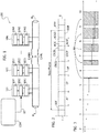
Figure 1 is a block diagram exemplary of a possible context of use of embodiments, -
Figure 2 illustrates a CAN frame, -
Figure 3 is a exemplary of the possible effect of clock inaccuracy of an oscillator in a context as exemplified inFigure 1 , -
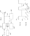
Figure 4 is a block diagram exemplary of a conventional approach in clock recovery, -
Figures 5A and 5B are time diagrams exemplary of possible operation of a circuit based on the concept outlined inFigure 4 , -
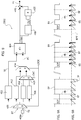
Figure 6 is a block diagram exemplary of embodiments as per the instant description, -
Figure 7 is a flow chart exemplary of possible operation of a circuit as per the block diagram ofFigure 6 , -
Figure 8 is a circuit diagram exemplary of a possible implementation of a solution as exemplified inFigure 6 , and -
Figures 9A and 9B are time diagrams exemplary of a possible time behavior of signals which may be present in embodiments of the present description. - In the following description, various specific details are given to provide a thorough understanding of various exemplary embodiments of the present specification. The embodiments may be practiced without one or several specific details, or with other methods, components, materials, etc. In other instances, well-known structures, materials, or operations are not shown or described in detail in order to avoid obscuring various aspects of the embodiments. Reference throughout this specification to "one embodiment" or "an embodiment" means that a particular feature, structure, or characteristic described in connection with the embodiment is included in at least one embodiment. Thus, the possible appearances of the phrases "in one embodiment" or "in an embodiment" in various places throughout this specification are not necessarily all referring to the same embodiment. Furthermore, particular features, structures, or characteristics may be combined in any suitable manner in one or more embodiments.
- The headings/references provided herein are for convenience only, and therefore do not interpret the extent of protection or scope of the embodiments.
- In
Figure 1 ,reference 100 denotes as a whole a network such as a Controller Area Network (CAN), that is a network including a bus (CAN bus) including "high" and "low" lines CANH and CANL terminated onto end resistors RT and having a plurality of N electronic control units (ECUs) 101, 102, ..., 10N coupled to the bus lines CANH, CANL. - The
individual ECUs - a
microcontroller - a
CAN controller - a
transceiver - A
CAN 100 as exemplified inFigure 1 provides a bus standard suited for use, for instance, in a vehicle context. - Due to the differential nature of the bus CANH, CANL, a
CAN 100 as exemplified herein exhibits a marked robustness against noise. - As a result of a message-based protocol being used, a
CAN 100 as exemplified herein also facilitates communication between microcontrollers and devices controlled thereby (not visible inFigure 1 ) without a host computer. - For instance, for each device the data in a frame can be transmitted in sequence by adopting a priority mechanism such that if plural devices transmit at the same time, a device having a higher/highest priority continues the transmission while the other, conflicting devices discontinue transmission. Frames as transmitted are received by all the devices coupled to the bus, including the transmitting device.
-
Figure 2 illustrates a conventional CAN frame, shown between two "bus idle" states designated I. - A frame as illustrated in
Figure 2 comprises the following fields: - Start Of Frame - SOF
- Arbitration Field - AF
- Control Field - CF
- Data Field - DF
- CRC Field - CRCF, in turn comprising a CRC (Cyclical Redundancy Check) sequence and a CRC delimiter CRCD
- ACK Field - ACKF, in turn comprising an acknowledgement slot bit and an ACK delimiter ACKD
- End Of Frame - EOF
- Intermission Field - ITM
- The CRC sequence in each frame consists of 15 bits.
- The value of these bits depends on all the previous bits (excluding possible stuffing bits) in the frame and is calculated by means of a polynomial, which for conventional frames (as illustrated here) is defined as: CRC_15 = C59916 = (x15+x14+x10+x8+x7+x4+x3+1).
- Each receiver in a
CAN 100 as exemplified inFigure 1 includes a decoder configured to calculate the CRC from the data received. If these are different from the data sent, the CRC calculated "internally" by the decoder will be different from the CRC received, and the frame is discarded. - Stated otherwise, such a CRC check involves a comparison of the CRC in the frame received and the CRC calculated in the receiver: if these CRC's are identical, the check is passed; otherwise it fails.
- The general concepts underlying the structure and operation of a
CAN network 100 as exemplified inFigures 1 and 2 are well known to those of skill in the art, which makes it unnecessary to provide a more detailed description herein. - A (partial) networking arrangement as exemplified in
Figure 1 may involve decoding the input bitstream received by each device (ECU) coupled to the bus, with such a bitstream expected to be asynchronous with respect to the internal oscillator of the device. - Consequently, a clock data recovery circuit CDR can be provided at each device (ECU) 101, 102, ..., 10N with the aim of synchronizing the internal oscillator to the input bitstream received by the device. For simplicity, only one such clock data recovery circuit is visible in
Figure 1 under the general assumption that similar circuits are provided for the other devices in thenetwork 100. - As known to those of skill in the art, operation of a
CAN network 100 as exemplified inFigure 1 may involve so-called recessive-to-dominant (REC-DOM) as well as dominant-to-recessive (DOM-REC) transitions. - As noted, a CAN bus uses differential wired-AND signals so that the lines CANH and CANL in the bus can be driven to a "dominant" state (during which CANH is at a higher voltage than CANL) or not driven and pulled by passive resistors such as RT to a "recessive" state (during which CANH is at a voltage lower or equal to the voltage at CANL).
- For instance, for transmission purposes:
- a "0" data bit can be encoded as a dominant state (DOM), and
- a "1" data bit can be encoded as a recessive state (REC).
- That solution (per se non-imperative) co-operates with the wired-AND connection in giving to devices having lower ID numbers priority for access to the bus as discussed previously.
- In such a context, synchronization can be advantageously performed on falling edges by taking into account that REC-DOM transitions are low-impedance driven and tend to be sharp, and thus better suited for synchronization purposes in comparison with DOM-REC transitions.
- For instance, synchronization may be based on measuring the number of bits between two subsequent (consecutive) falling edges, that is first and second homologous edges (both falling edges, for instance) having no homologous (again falling, for instance) third edge therebetween.
- In that respect it will be appreciated that while reference to a CAN bus is made throughout this detailed description for simplicity and ease of understanding, the same type of operation and the underlying considerations may be applied also to other bus types operating on similar principles.
- Stated otherwise, reference to a CAN bus and, more to the point, reference to a CAN network is merely for exemplary purposes and is not to be construed, even indirectly, in a limiting sense of embodiments.
- In certain contexts of operation, bit-stuffing may be adopted, that is, allowing a maximum number of consecutive coincident bits, such as 5 (five). Consequently, two subsequent consecutive synchronization edges within a same frame may come, at a maximum distance of, for instance, 2x5=10 bit periods.
-
Figure 2 is exemplary of the possible effect of oscillator period error in a sequence of bits. Taking into account that the minimum distance between two falling edges is 2 bits, an oscillator period error (+/-10%, for instance) may gradually lead to increasingly ambiguous values AV for those bits gradually coming near to the maximum distance discussed in the foregoing, namely 2x5=10 bit periods, for instance. -
Figure 4 is a block diagram exemplary of a clock data recovery circuit CDR comprising a frequency locking system configured to lock the frequency of an oscillator internal to a certain device (any of theECUs Figure 1 being possibly exemplary of such a device) to the bitrate (frequency) of an incoming received signal RX. - In the block diagram of
Figure 4 ,reference 1000 denotes a timer circuit configured to generate a sawtooth signal BT (bit time) having a slope intended to be tuned. - As exemplified in
Figures 5A and 5B , such tuning action may have the target of causing the "tips" of the sawtooth signal (that is the points where the signal BT reaches a period threshold BPT) to coincide with the actual bit falling edges BE, so that the signal BT may be adjusted to have a period equal to the bit time of the input signal RX. In that way the signal BT can used to generate a strobe signal BS useful in sampling the input bitstream (see also BS as illustrated inFigure 9B ) . - As exemplified in
Figure 4 , the output from the timer 1000 (bit time signal BT) is fed to a frequencyerror extraction circuit 1002. Thecircuit 1002 is configured to extract a current oscillator frequency error by comparing the actual oscillator period with the bit edges BE of the incoming signal RX thus generating a frequency error signal FE. - As exemplified in
Figure 4 , the frequency error signal FE is fed to a loopfilter integrator circuit 1004 configured to integrate the bit period error over multiple transitions (see the time error TE inFigure 5B ) and produce a signal SC which is supplied to thetimer 1000 for adjusting the slope of the sawtooth signal generated by thetimer circuit 1000 so that, as a result of the slope adjustment (as exemplified by SC inFigure 5B ), the signal BT reaches a desired bit period threshold BPT at the time of a bit edge BE. - As exemplified in
Figure 4 , adjustment of the slope of the sawtooth signal generated by thetimer circuit 1000 via the adjustment signal exemplified by SC takes into account a compensation signal from a feed-forward compensation circuit 1006 which is injected at anode 1008 in the signal propagation path from the loopfilter integration circuit 1004 to thetimer circuit 1000. - As noted, possible operation of a (conventional) arrangement as exemplified in
Figure 4 is illustrated in the time diagrams ofFigures 5A, 5B which represent, against a common time (abscissa) scale t: - the input signal RX having bit edges BE (
Figure 5A ), - the bit-time signal BT, the (accumulated) timing error deriving from the frequency error FE in
Figure 4 and the slope correction action via the signal SC towards the threshold BPT (Figure 5A ). - As noted, operation of a clock data recovery circuit CDR as exemplified in
Figure 4 may take advantage of the sharper REC-DOM transitions (if applied to a CAN bus) and involve: - integrating the error over multiple transitions assuming a certain maximum number of bits between two subsequent falling edges (for instance 2x5 = 10, resulting from bit-stuffing), and
- adjusting the slope of signal from the
timer circuit 1000 correspondingly. - Feed-forward compensation as exemplified by 1006 and 1008 in
Figure 4 facilitates recovery of oscillator period deviation versus temperature. - As discussed, compensation may involve interpolating deviations of the oscillator period based on plural (three, for instance) error values obtained during an (automated) testing action and stored in a memory (OTP, for instance) which may be regarded as included in the
block 1006 inFigure 4 . - Correct locking of the input signal RX may thus be achieved in a solution as exemplified in
Figure 4 provided the difference between the linear interpolation and the actual period error of the oscillator lies within a certain limit (+/-5% for instance). - Irrespective of this, a solution as exemplified in
Figure 4 suffers from drawbacks related to the test time (automated trimming procedures) and the semiconductor area occupied by the digital logic and the OTP registers which may be included in theblock 1006. - These issues are addressed by embodiments as exemplified in
Figure 6 . - In the block diagram of
Figure 6 , atimer circuit 2000 is shown configured to receive the input signal RX and send a bit time signal BT towards a frequencyerror extraction circuit 2002. This is in turn configured for generating a frequency error signal FE to be supplied to aloop filter integrator 2004, which produces a slope correction signal SC which is supplied to thetimer circuit 2000. - The same designations and/or reference symbols are used in
Figure 4 andFigure 6 for the timer circuit, the frequency error extraction circuit and the loop filter integrator as well as for the bit-time signal, the frequency error signal and the slope correction signal. - Such a choice is intended to facilitate comparison for ease of explanation and understanding: it will be otherwise appreciated that circuits/signals having like designations in
Figures 4 and6 are not necessarily implemented in the same way and/or do not necessarily have identical time behaviors. - In embodiments as exemplified in
Figure 6 (and as further discussed in the following) the frequencyerror extraction circuit 2002 generates frequency error signals FE on the basis of: - the signal BT from the
timer circuit 2000, and - a signal CRC indicating the outcome of a redundancy check (such as a Cyclic Redundancy Check, briefly CRC) from a
frame decoder circuit 2006 which in turn receives a sampled bit-signal SB from a bit-strobe circuit 2008 sensitive to both the input signal RX and the signal BT from thetimer circuit 2000. - In one or more embodiments as exemplified in
Figure 6 , (where again the sawtooth signal BT from thetimer circuit 2000 can be used to produce a strobe signal BS useful in sampling the input bitstream - see also BS as illustrated inFigure 9B ) bit-time ambiguity as due to an error in the clock generation action can be resolved by "trying" two possible values in two subsequent/consecutive frames, with a redundancy check such as a Cyclic Redundancy Check (CRC) used to validate the result of selection (selected choice). - By way of general explanation, in one or more embodiments such ambiguity may be resolved along the lines of the flowchart of
Figure 7 . - An action as exemplified at 300 involves using a first (synchronization or synch) frame in the signal RX to measure the time between two subsequent homologous edges, that is two edges of the same type (falling edges, for instance) coming one after the other with no edges of the same type occurring therebetween: for instance, two falling edges coming one after the other with a rising edge therebetween represent two subsequent homologous edges as intended herein.
- As exemplified in
Figure 7 , the action as exemplified at 300 is performed while the slope of the sawtooth signal generated by thetimer 2000 is adjusted to a first value, which may be assumed to correspond to a first "floor" (lower) value. - An action as exemplified at 302 involves a corresponding measurement performed "internally" (that is at the
receivers - For instance, in one or more embodiments, the comparison performed at 304 may involve a comparison of the CRC calculated internally with the CRC field of the received bitstream.
- If the check at 304 yields a positive outcome (CRC correct, outcome from 304 = Y), the previous slope value as determined on the basis of the time between two consecutive edges measured on the first synch frame is validated and a "locked" flag is asserted at 306 with the validated value used as starting point of the loop filter.
- If, conversely, the check at 304 yields a negative outcome (CRC not correct) a different, second slope value is set at 308, for instance a value obtained replacing the first "floor" value with a second "ceiling" (higher) value and system operation returns to 302.
- One or more embodiments may contemplate that, if the check at 304 fails repeatedly (for instance three or more times in a row), an error state can be declared as exemplified by 310.
- In one or more embodiments as exemplified in
Figure 6 , the bit-strobe generator circuit 2008 can be configured to select the sampling point of the bit time at the "raw data" signal RX and theframe decoder circuit 2006 can be configured to implement a wake-up feature and (also) to validate the slope correction by implementing the CRC check ofstep 304 inFigure 7 , with the CRC signal assuming different logical values corresponding to the outcome ofstep 304 being either Y or N. - The block diagram of
Figure 8 is exemplary of a possible implementation of the frequency error extraction circuitry in the exemplary block diagram ofFigure 6 , wherein thecircuit 2002 is intended to be sensitive to a signal from the timer 2000 (this may simply correspond to the time between two consecutive falling edges) and the CRC signal from the frame decoder 2006 (configured to perform the CRC check ofstep 304 ofFigure 7 ). - As exemplified in
Figure 8 the frequency error extraction circuitry may comprise aninput multiplexer 400 receiving the time signal BT from thetimer circuit 2000 and a measured time value (from amemory 400a, for instance) which facilitates validation of a correct slope using a same timer value for two subsequent trials as discussed previously. - The output from the
multiplexer 400 is supplied to anerror extraction circuit 402 which generates a total error signal TE to be supplied to a first input (designated a) of an a/b divider 404. - The output from the
multiplexer 400 is also supplied to twocircuits multiplexer 410. - The output from the
multiplexer 400 is also supplied to a roundingcircuit 412 so that afurther multiplexer 414 may receive (to be supplied to a second input, marked b, of the a/b divider 404) a bit count signal BC given by either one of: - the output from the
multiplexer 410, that is - in turn - the output from either one of thefloor value 406 or theceiling value 408, - the output signal from a rounding
circuit 412. - In simple explanatory terms, in operation of a circuit as exemplified in
Figure 8 , once a lock condition is achieved (step 306 inFigure 7 ) a LOCK signal applied to themultiplexers timer circuit 2000 being forwarded to the input b of thedivider 404 via the roundingcircuit 412, so that, after the lock phase, a bit count signal BC applied to the input b can be evaluated just by rounding the timer signal. - Conversely, prior to locking achieved, the a/
b divider 404 will be supplied via themultiplexer 414 with either one of the floor or ceiling values from thecircuits - In embodiments as exemplified in
Figure 8 , the output from the a/b divider 404 can be a signal including a total number of bits (17, for instance) including a sign bit plus integer bits and fractional bits with a number of fractional bits equal, for instance, to 16. - In embodiments as exemplified herein, the signal from the
switch 404 can be supplied to a summation node (with sign) 416 which can be configured to generate the frequency error signal FE by combining (subtracting) from the output signal from thedivider 404 an interpolated value obtained by converting at aconverter 418 the signal from thedivider 404 to a shorter format such as, for instance, a signal in a format s4/6 obtained from the s17/16 signal from thedivider 404 with subsequent generation, at a circuit 420 (a multiplier for instance) of a second order term of a Taylor series. - By way of summary, a synchronization procedure as discussed herein has the purpose of reducing (notionally to zero) the time error between the internal oscillators of the units (ECUs) 101, 102, ..., 10N coupled to the bus lines CANH, CANL and the bitstream transmitted thereon.
- If referred to a single bit, such an error can be defined as:

Figure 5B ) and BC is the number of bits between two falling edges ( TEB is the output of thedivider 404 inFigure 8 ). - An accurate error estimate thus involves correctly determining the value for BC. This is calculated "internally" at each
unit 
- In arrangements as exemplified in
Figure 4 the value for BC is rounded to the nearest integer. This is facilitated by the error on the oscillator period being reduced below +/-5% (for instance) using the feedforward compensation at 1006, so that a univocal value can be calculated for BC. - As discussed, in the presence of a larger error (+/-10%, for instance) BC is no longer univocal, as exemplified in
Figure 3 . - Using an erroneous value for BC militates against correct CDR synchronization with the received bitstream (within five frames, as specified by ISO standards) and may result in loop filter divergence.
- The dependency of BC on the error in the clock period can be expressed as follows:


Tosc is the period of the oscillator
εosc is the error affecting oscillator period
TB is the time duration of one bit
N is the number of clock pulses between two subsequent falling edges
BC real is the number of bits actually present between two subsequent falling edges
BC is the number of bits calculated digitally
OVS is the oversampling factor. - In one or more embodiments, the non-uniqueness of BC is solved by using a CRC check as a discriminating factor to decide whether rounding shall take place up or down (e.g. "ceiling" or "floor").
- In fact, BC can be used to produce strobe signals (see BS in
Figure 9B as discussed in the following) used to sample the bits received: an erroneous value for BC leads to an erroneous decoding of received frames and to an ensuing failure of the CRC check. - Once a correct value for BC is identified (which may be seen as corresponding to the first measurement at 300 in
Figure 7 ), the slope of the ramp SC is updated (see SC inFigure 5B by way of reference) so that the subsequent error value (that is TEB ) will be reduced (to less than ±5%, for instance. - Then the loop filter (see 2002, 2004 in
Figure 6 , for instance) may produce a slope correction signal SC which is supplied to thetimer circuit 2000, by simply rounding BC to the nearest integer. - Correcting the slope of a periodic signal amounts to varying its frequency, so that an error on the period can be converted into a frequency error FE (see
Figure 8 ):
- As exemplified in
Figure 8 this may involve providing: - a
subtraction node 416, - a
digital signal converter 418 from s17/16 to s4/6, - a 4-
bit multiplier 420. - Using a converter such as 418 facilitates using a multiplier having (only) 4 bits which results in an appreciable area saving in comparison to a multiplier having 16-bit (that is the original signal size). It is noted that the information loss due to conversion, is negligible insofar as the error signal exhibits reduced dynamics (+/-0.1, for instance).
-
Figures 9A and 9B represent superposed diagrams sharing a common time scale (abscissa) wherein possible time behaviors/positions are shown for: - the input signal RX having bit-edges at BE,
- the bit-signal BT from the
timer circuit 2000 - the strobe threshold ST applied by the bit-
strobe generator circuit 2008 - the bit-strobe signal BS comprising pulses generated as result of the bit-signal BT (a sawtooth signal, as exemplified) reaching the strobe threshold ST.
- The leftmost portions of
Figures 9A and 9B are exemplary of a total error TE with reference to a "first" falling edge indicative the start of frame (SOF) condition. - This may correspond, for instance, to the first measured time discussed previously in connection with
step 300 inFigure 7 and a measured time corresponding to 5.5 (this is a purely exemplary value). - This is exemplary of a frame (including five bits having respective bit-edges BE shown in dashed lines) found to correspond to five periods and half (namely 5.5 periods) of the sawtooth signal from the
timer circuit 2000. - The central portions of
Figures 9A and 9B are exemplary of a (first) decoding step at 302 inFigure 7 performed using a first value (floor=0, for instance) which results in six bit-strobe pulses BS, that is a bit-count equal to six and a corresponding negative outcome of the check at astep 304 ofFigure 7 . - For simplicity,
Figures 9A and 9B show just the initial portion of the frames. Since the decoder is evaluating a bit-stream different from the real one (e.g. "0111110..." instead of "011110 ...") the "internal" CRC value will be different from the one of the bit-stream and so the CRC check will fail (outcome N ofstep 304 inFigure 7 - (CRC_OK=0). - Conversely, the rightmost portions of
Figures 9A and 9B are exemplary of a (further) decoding performed after slope correction as exemplified byblock 308 inFigure 7 . This time the decoder will be evaluating a bit-stream corresponding to the real one and the "internal" CRC value will be the same as the one of the bit-stream and so the CRC check will succeed (outcome Y ofstep 304 inFigure 7 - (CRC_OK=1). A lock condition will thus be affirmed as exemplified byblock 306 inFigure 7 , with the bit-count signal subsequently evaluated just by rounding the timer signal (circuit 412) . - A method as exemplified herein may comprise:
- receiving (for instance, 300, 2008) at a receiver (for instance, 101, 102, ..., 10N) an input signal (for instance, RX) arranged in frames, the frames including at least one field (for instance, CRCF) including a certain number of bits having bit edges (for instance, BE),
- producing (for instance, 302, 2000) at said receiver a timing signal (for instance, BT) including waveforms having a duration adjustable (for instance, SC, 410) at one of a first duration value (for instance, 406) and a second duration value (for instance, 408),
- performing a check (for instance, 304, 2006) as to the occurrence, over the duration of said number of bits having bit edges in said bit frames in said received input signal, of a number of waveforms of said timing signal having said duration adjusted to one of said first duration value and said second duration value which corresponds to said number of bits having bit edges,
- producing a check signal (for instance, CRC) having a first (pass) value (for instance, Y) or a second (fail) value (for instance, N) as a function of whether said check is passed or failed, and
- as a result of said check signal having said first value, maintaining (for instance, 306) the duration of the waveforms in said timing signal adjusted to said one of said first duration value and said second duration value,
- as a result of said check signal having said second value, re-adjusting (for instance, 308) the duration of the waveforms in said timing signal to the other of said first duration value and said second duration value.
- In a method as exemplified herein:
- said timing signal may comprise a sawtooth signal including sawtooth waveforms with slope values adjustable at one of a first slope value and a second slope value, and
- the method may comprise:
- as a result of said check signal having said first value, maintaining said slope of the sawtooth waveforms adjusted to said one of said first slope value and said second slope value,
- as a result of said check signal having said second value, re-adjusting said slope of the sawtooth waveforms to the other of said first slope value and said second slope value.
- A method as exemplified herein may comprise, as a result of said check signal having said first value, rounding to the nearest integer (for instance, 412) the number of waveforms (for instance, BC) of said timing signal occurring over the duration of said bit frames in said received input signal.
- A method as exemplified herein may comprise:
- producing (for instance, 402) a timing error signal (for instance, TE) indicative of the time offset of said timing signal with respect to the received input signal,
- as a result of said check signal having said first value, producing (for instance, 2000) a strobe signal (for instance, BS) for sampling said input signal, wherein the frequency of said strobe signal is varied as a function (see, for instance, 404, 406, 408, 410, 412, 414, 4461, 418, 420) of said timing error signal targeting (that is, having as a target) synchronizing said strobe signal with the bit edges in said input signal.
- In a method as exemplified herein, producing (2000) said strobe signal may comprise:
- generating (for instance, 406, 408, 410, 412, 414) a count value (for instance, BC) indicative of the number of waveforms of said timing signal occurring over the duration of said bit frames in said received input signal,
- dividing (for instance, 404) said timing error signal by said count value to produce a per-bit timing error signal,
- varying the frequency of said strobe signal as a function of said per-bit timing error signal targeting synchronizing said strobe signal with the bit edges in said input signal.
- A method as exemplified herein may comprise converting (for instance, 416, 418, 420) said per-bit timing error signal to a frequency error signal (for instance, FE), wherein the frequency of said strobe signal is varied as a function of said frequency error signal.
- In a method as exemplified herein, converting said per-bit timing error signal to a frequency error signal may comprises reducing the bit resolution (for instance, from s17/16 to S4/4) of the result of said dividing said timing error signal by said count value.
- A method as exemplified herein may comprise, as a result of said check failing with said check signal having said second value over a certain number of said frames, declaring an error state (for instance, 310).
- In a method as exemplified herein, said at least one field (for instance, CRCF) includes a set of bits comprised between two subsequent homologous bit edges in said input signal.
- In a method as exemplified herein, said two subsequent homologous bit edges in said input signal may comprise two subsequent falling edges in said input signal having no falling edges therebetween.
- In a method as exemplified herein:
- said input signal may comprise a cyclic redundancy check sequence (CRC) in said at least one field (for instance, CRCF) including a certain number of bits having bit edges,
- said check as to the occurrence, over the duration of said number of bits having bit edges in said bit frames in said received input signal, of said number of waveforms of said timing signal may comprise a cyclic redundancy check as a function of said cyclic redundancy check sequence (CRC).
- A circuit (for instance, CDR) configured to implement a method as exemplified herein may comprise:
- receiver circuitry (for instance, 2008) configured to receive said input signal arranged in frames including at least one field including a certain number of bits having bit edges,
- timer circuitry (for instance, 2000, 2002, 2004) configured to produce said timing signal including waveforms having a duration adjustable at one of a first duration value and a second duration value,
- check circuitry (for instance, 2006) configured to perform said check as to the occurrence, over the duration of said number of bits having bit edges in said bit frames in said received input signal, of a number of waveforms of said timing signal having said duration adjusted to one of said first duration value and said second duration value which corresponds to said number of bits having bit edges (BE) and producing said check signal having a first value or a second value as a function of whether said check is passed or failed, and
- said timer circuitry configured to maintain the duration of the waveforms in said timing signal adjusted to said one of said first duration value and said second duration value or to re-adjust the duration of the waveforms in said timing signal to the other of said first duration value and said second duration value as a result of said check signal having said first value or said second value, respectively.
- A system (for instance, 100) as exemplified herein may comprise a network of devices (for instance, 101, 102, ..., 10N) coupled via a bus (for instance, CANH, CANL) and configured to exchange over said bus communication signals arranged in frames, the frames including at least one field including a certain number of bits having bit edges,
wherein the devices in said network may comprise respective circuits (for instance, CDR) configured to receive said communication signals arranged in frames and produce respective timing signals frequency-locked to said communication signals exchanged over said bus. - In a system as exemplified herein, said bus may comprise a CAN bus.
- Without prejudice to the underlying principles, the details and embodiments may vary, even significantly, with respect to what has been described by way of example only without departing from the extent of protection. The extent of protection is determined by the annexed claims.
Claims (13)
- A method, comprising:receiving (300, 2008) at a receiver (101, 102, ..., 10N) an input signal (RX) arranged in frames, the frames including at least one field (CRCF) including a certain number of bits (BE) comprised between two subsequent homologous bit edges in said input signal (RX),producing (302, 2000) at said receiver (101, 102, ..., 10N) a timing signal (BT) including waveforms each having a duration adjustable (SC, 410) at one of a first duration value (406) and a second duration value (408),performing a check (304, 2006) as to the occurrence, over the duration of said number of bits (BE) comprised between two subsequent homologous bit edges in said input signal (RX) in said bit frames in said received input signal (RX), of a number of waveforms of said timing signal (BT) having said duration adjusted to one of said first duration value (406) and said second duration value (408) by checking whether said number of waveforms corresponds to said number of bits (BE) comprised between two subsequent homologous bit edges in said input signal (RX),producing a check signal (CRC) having a first value (Y) or a second value (N) as a function of whether said check (304) is passed or failed, andas a result of said check signal (CRC) having said first value (Y), maintaining (306) the duration of the waveforms in said timing signal (BT) adjusted to said one of said first duration value (406) and said second duration value (408),as a result of said check signal (CRC) having said second value (N), re-adjusting (308) the duration of the waveforms in said timing signal (BT) to the other of said first duration value (406) and said second duration value (408).
- The method of claim 1, wherein:said timing signal (BT) comprises a sawtooth signal (BT) including sawtooth waveforms with slope values adjustable (SC, 410) at one of a first slope value(406) and a second slope value (408), andthe method comprises:as a result of said check signal (CRC) having said first value (Y), maintaining (306) said slope of the sawtooth waveforms (BT) adjusted to said one of said first slope value (406) and said second slope value (408),as a result of said check signal (CRC) having said second value (N), re-adjusting (308) said slope of the sawtooth waveforms (BT) to the other of said first slope value (406) and said second slope value (408).
- The method of claim 1 or claim 2, comprising, as a result of said check signal (CRC) having said first value (Y), rounding to the nearest integer (412) the number of waveforms (BC) of said timing signal (BT) occurring over the duration of said bit frames in said received input signal (RX).
- The method of any of the previous claims, comprising:producing (402) a timing error signal (TE) indicative of the time offset of said timing signal (BT) with respect to the received input signal (RX),as a result of said check signal (CRC) having said first value (Y), producing (2000) a strobe signal (BS) for sampling said input signal (RX), wherein the frequency of said strobe signal (BS) is varied as a function (404, 406, 408, 410, 412, 414, 4461, 418, 420) of said timing error signal (TE) targeting synchronizing said strobe signal (BS) with the bit edges (BE) in said input signal (RX).
- The method of any of claim 4, wherein producing (2000) said strobe signal (BS) comprises:generating (406, 408, 410, 412, 414) a count value (BC) indicative of the number of waveforms (BC) of said timing signal (BT) occurring over the duration of said bit frames in said received input signal (RX),dividing (404) said timing error signal (TE) by said count value (BC) to produce a per-bit timing error signal,varying the frequency of said strobe signal (BS) as a function of said per-bit timing error signal targeting synchronizing said strobe signal (BS) with the bit edges (BE) in said input signal (RX).
- The method of claim 5, comprising converting (416, 418, 420) said per-bit timing error signal to a frequency error signal (FE), wherein the frequency of said strobe signal (BS) is varied as a function of said frequency error signal (FE).
- The method of claim 6, wherein converting (416, 418, 420) said per-bit timing error signal to a frequency error signal (FE) comprises reducing the bit resolution (s17/16 to S4/4) of the result of said dividing (404) said timing error signal (TE) by said count value (BC).
- The method of any of the previous claims, comprising, as a result of said check (304) failing with said check signal (CRC) having said second value (N) over a certain number of said frames, declaring an error state (310).
- The method of any of the previous claims, wherein said two subsequent homologous bit edges in said input signal (RX) comprise two subsequent falling edges in said input signal (RX) having no falling edges therebetween.
- The method of any of the previous claims, wherein:said input signal (RX) comprises a cyclic redundancy check sequence (CRC) in said at least one field (CRCF) including a certain number of bits (BE) comprised between two subsequent homologous bit edges in said input signal (RX),said check (304) as to the occurrence, over the duration of said number of bits (BE) comprised between two subsequent homologous bit edges in said input signal (RX) in said bit frames in said received input signal (RX), of said number of waveforms of said timing signal (BT) comprises a cyclic redundancy check as a function of said cyclic redundancy check sequence (CRC).
- A circuit (CDR) configured to implement the method of any of claims 1 to 10 and comprising:receiver circuitry (2008) configured to receive said input signal (RX) arranged in frames including at least one field (CRCF) including a certain number of bits (BE) comprised between two subsequent homologous bit edges in said input signal (RX),timer circuitry (2000, 2002, 2004) configured to produce said timing signal (BT) including waveforms having a duration adjustable (SC, 410) at one of a first duration value (406) and a second duration value (408),check circuitry (2006) configured to perform said check (304) as to the occurrence, over the duration of said number of bits (BE) comprised between two subsequent homologous bit edges in said input signal (RX)in said bit frames in said received input signal (RX), of a number of waveforms of said timing signal (BT) each having said duration adjusted to one of said first duration value (406) and said second duration value (408) which corresponds to said number of bits (BE) comprised between two subsequent homologous bit edges in said input signal (RX) and producing said check signal (CRC) having a first value (Y) or a second value (N) as a function of whether said check (304) is passed or failed, andsaid timer circuitry (2000, 2002, 2004) configured to maintain the duration of the waveforms in said timing signal (BT) adjusted to said one of said first duration value (406) and said second duration value (408) or to re-adjust (308) the duration of the waveforms in said timing signal (BT) to the other of said first duration value (406) and said second duration value (408) as a result of said check signal (CRC) having said first value (Y) or said second value (N), respectively.
- A system (100), comprising a network of devices (101, 102, ..., 10N) coupled via a bus (CANH, CANL) and configured to exchange over said bus (CANH, CANL) communication signals (RX) arranged in frames, the frames including at least one field (CRCF) including a certain number of bits (BE) comprised between two subsequent homologous bit edges in said input signal (RX),
wherein the devices (101, 102, ..., 10N) in said network comprise respective circuits (CDR) according to claim 11, said respective circuits (CDR) configured to receive (300) said communication signals (RX) arranged in frames and produce (2000) respective timing signals (BT) frequency-locked to said communication signals (RX) exchanged over said bus (CANH, CANL). - The system (100) of claim 12, wherein said bus (CANH, CANL) comprises a CAN bus.
Applications Claiming Priority (1)
| Application Number | Priority Date | Filing Date | Title |
|---|---|---|---|
| IT102020000013222A IT202000013222A1 (en) | 2020-06-04 | 2020-06-04 | CLOCK RECOVERY PROCESS, CORRESPONDING CIRCUIT AND SYSTEM |
Publications (2)
| Publication Number | Publication Date |
|---|---|
| EP3920460A1 true EP3920460A1 (en) | 2021-12-08 |
| EP3920460B1 EP3920460B1 (en) | 2022-11-02 |
Family
ID=72087091
Family Applications (1)
| Application Number | Title | Priority Date | Filing Date |
|---|---|---|---|
| EP21175058.3A Active EP3920460B1 (en) | 2020-06-04 | 2021-05-20 | Clock recovery method, corresponding circuit and system |
Country Status (3)
| Country | Link |
|---|---|
| US (1) | US11637683B2 (en) |
| EP (1) | EP3920460B1 (en) |
| IT (1) | IT202000013222A1 (en) |
Citations (3)
| Publication number | Priority date | Publication date | Assignee | Title |
|---|---|---|---|---|
| US6389548B1 (en) * | 1999-04-12 | 2002-05-14 | Liam Bowles | Pulse run-length measurement for HF data signal by dividing accumulated phase difference between first and second zero-crossings by single-cycle range using multiple cycle range sawtooth waveform |
| WO2014191788A1 (en) | 2013-05-29 | 2014-12-04 | Freescale Semiconductor, Inc. | A network receiver for a network using distributed clock synchronization and a method of sampling a signal received from the network |
| US20200076643A1 (en) | 2018-08-28 | 2020-03-05 | Texas Instruments Incorporated | Controller area network receiver |
Family Cites Families (4)
| Publication number | Priority date | Publication date | Assignee | Title |
|---|---|---|---|---|
| JP3323809B2 (en) * | 1998-06-19 | 2002-09-09 | 松下電器産業株式会社 | Time-division multiplexed wireless communication reception field strength measurement device |
| CN101171790B (en) * | 2005-05-02 | 2011-11-30 | Nxp股份有限公司 | Receiver with Adaptive Gate Offset Adjustment |
| JP5751290B2 (en) * | 2013-07-11 | 2015-07-22 | 株式会社デンソー | Data receiving device and method for determining same bit length of received bit string |
| US10614016B2 (en) * | 2015-10-20 | 2020-04-07 | Nxp B.V. | Controller area network (CAN) device and method for operating a CAN device |
-
2020
- 2020-06-04 IT IT102020000013222A patent/IT202000013222A1/en unknown
-
2021
- 2021-05-20 EP EP21175058.3A patent/EP3920460B1/en active Active
- 2021-06-01 US US17/335,336 patent/US11637683B2/en active Active
Patent Citations (3)
| Publication number | Priority date | Publication date | Assignee | Title |
|---|---|---|---|---|
| US6389548B1 (en) * | 1999-04-12 | 2002-05-14 | Liam Bowles | Pulse run-length measurement for HF data signal by dividing accumulated phase difference between first and second zero-crossings by single-cycle range using multiple cycle range sawtooth waveform |
| WO2014191788A1 (en) | 2013-05-29 | 2014-12-04 | Freescale Semiconductor, Inc. | A network receiver for a network using distributed clock synchronization and a method of sampling a signal received from the network |
| US20200076643A1 (en) | 2018-08-28 | 2020-03-05 | Texas Instruments Incorporated | Controller area network receiver |
Also Published As
| Publication number | Publication date |
|---|---|
| EP3920460B1 (en) | 2022-11-02 |
| US11637683B2 (en) | 2023-04-25 |
| US20210385059A1 (en) | 2021-12-09 |
| IT202000013222A1 (en) | 2021-12-04 |
Similar Documents
| Publication | Publication Date | Title |
|---|---|---|
| US8566632B2 (en) | Multi-rate sampling for network receiving nodes using distributed clock synchronization | |
| EP1355458B1 (en) | Method for transmitting data within a communication system | |
| EP0679307B1 (en) | Delay line separator for data bus | |
| EP0726662A2 (en) | Receiver and transmitter-receiver | |
| Hartwich et al. | The configuration of the CAN bit timing | |
| JPH04320109A (en) | Circuit for discriminating transition phase of data edge | |
| US20110026572A1 (en) | Baud rate error detection circuit and baud rate error detection method | |
| US11799578B2 (en) | Time synchronization method and device, network node device | |
| US6850580B1 (en) | Bit synchronizing circuit | |
| US20160087737A1 (en) | A network receiver for a network using distributed clock synchronization and a method of sampling a signal received from the network | |
| Smirnov et al. | Formal reliability analysis of switched ethernet automotive networks under transient transmission errors | |
| EP3920460B1 (en) | Clock recovery method, corresponding circuit and system | |
| EP3005605B1 (en) | A network receiver for a network using distributed clock synchronization and a method of adjusting a frequency of an internal clock of the network receiver | |
| US8711996B2 (en) | Methods and apparatus for determining a phase error in signals | |
| EP1335520A1 (en) | Multiplex bus system with duty cycle correction | |
| US9509491B2 (en) | Data reception apparatus and method of determining identical-value bit length in received bit string | |
| CN112765073A (en) | Data sampling method, system, storage medium and computer equipment | |
| KR101746203B1 (en) | Method and Apparatus for Calibrating Phase Difference of Clock Signal between Chip and Chip in Multi Chip System | |
| US8311173B2 (en) | Frame pulse signal latch circuit and phase adjustment method | |
| US7551702B2 (en) | Method and circuit arrangement for synchronizing a function unit with a predetermined clock frequency | |
| CN101051837B (en) | Frequency Correction Device and Method for USB Interface Built-in Oscillator | |
| JP2848800B2 (en) | Serial digital signal sampling method | |
| CN112260814B (en) | Data phase correction method for high-speed serial communication, electronic device, and storage medium | |
| CN113765835B (en) | Semiconductor devices and decoding methods | |
| JP3178612B2 (en) | Phase synchronous clock extraction circuit |
Legal Events
| Date | Code | Title | Description |
|---|---|---|---|
| PUAI | Public reference made under article 153(3) epc to a published international application that has entered the european phase |
Free format text: ORIGINAL CODE: 0009012 |
|
| STAA | Information on the status of an ep patent application or granted ep patent |
Free format text: STATUS: THE APPLICATION HAS BEEN PUBLISHED |
|
| AK | Designated contracting states |
Kind code of ref document: A1 Designated state(s): AL AT BE BG CH CY CZ DE DK EE ES FI FR GB GR HR HU IE IS IT LI LT LU LV MC MK MT NL NO PL PT RO RS SE SI SK SM TR |
|
| B565 | Issuance of search results under rule 164(2) epc |
Effective date: 20211103 |
|
| STAA | Information on the status of an ep patent application or granted ep patent |
Free format text: STATUS: REQUEST FOR EXAMINATION WAS MADE |
|
| 17P | Request for examination filed |
Effective date: 20220208 |
|
| RBV | Designated contracting states (corrected) |
Designated state(s): AL AT BE BG CH CY CZ DE DK EE ES FI FR GB GR HR HU IE IS IT LI LT LU LV MC MK MT NL NO PL PT RO RS SE SI SK SM TR |
|
| GRAP | Despatch of communication of intention to grant a patent |
Free format text: ORIGINAL CODE: EPIDOSNIGR1 |
|
| STAA | Information on the status of an ep patent application or granted ep patent |
Free format text: STATUS: GRANT OF PATENT IS INTENDED |
|
| INTG | Intention to grant announced |
Effective date: 20220624 |
|
| GRAS | Grant fee paid |
Free format text: ORIGINAL CODE: EPIDOSNIGR3 |
|
| GRAA | (expected) grant |
Free format text: ORIGINAL CODE: 0009210 |
|
| STAA | Information on the status of an ep patent application or granted ep patent |
Free format text: STATUS: THE PATENT HAS BEEN GRANTED |
|
| AK | Designated contracting states |
Kind code of ref document: B1 Designated state(s): AL AT BE BG CH CY CZ DE DK EE ES FI FR GB GR HR HU IE IS IT LI LT LU LV MC MK MT NL NO PL PT RO RS SE SI SK SM TR |
|
| REG | Reference to a national code |
Ref country code: GB Ref legal event code: FG4D |
|
| REG | Reference to a national code |
Ref country code: CH Ref legal event code: EP Ref country code: AT Ref legal event code: REF Ref document number: 1529565 Country of ref document: AT Kind code of ref document: T Effective date: 20221115 |
|
| REG | Reference to a national code |
Ref country code: DE Ref legal event code: R096 Ref document number: 602021000668 Country of ref document: DE |
|
| REG | Reference to a national code |
Ref country code: IE Ref legal event code: FG4D |
|
| REG | Reference to a national code |
Ref country code: LT Ref legal event code: MG9D |
|
| REG | Reference to a national code |
Ref country code: NL Ref legal event code: MP Effective date: 20221102 |
|
| REG | Reference to a national code |
Ref country code: AT Ref legal event code: MK05 Ref document number: 1529565 Country of ref document: AT Kind code of ref document: T Effective date: 20221102 |
|
| PG25 | Lapsed in a contracting state [announced via postgrant information from national office to epo] |
Ref country code: SE Free format text: LAPSE BECAUSE OF FAILURE TO SUBMIT A TRANSLATION OF THE DESCRIPTION OR TO PAY THE FEE WITHIN THE PRESCRIBED TIME-LIMIT Effective date: 20221102 Ref country code: PT Free format text: LAPSE BECAUSE OF FAILURE TO SUBMIT A TRANSLATION OF THE DESCRIPTION OR TO PAY THE FEE WITHIN THE PRESCRIBED TIME-LIMIT Effective date: 20230302 Ref country code: NO Free format text: LAPSE BECAUSE OF FAILURE TO SUBMIT A TRANSLATION OF THE DESCRIPTION OR TO PAY THE FEE WITHIN THE PRESCRIBED TIME-LIMIT Effective date: 20230202 Ref country code: LT Free format text: LAPSE BECAUSE OF FAILURE TO SUBMIT A TRANSLATION OF THE DESCRIPTION OR TO PAY THE FEE WITHIN THE PRESCRIBED TIME-LIMIT Effective date: 20221102 Ref country code: FI Free format text: LAPSE BECAUSE OF FAILURE TO SUBMIT A TRANSLATION OF THE DESCRIPTION OR TO PAY THE FEE WITHIN THE PRESCRIBED TIME-LIMIT Effective date: 20221102 Ref country code: ES Free format text: LAPSE BECAUSE OF FAILURE TO SUBMIT A TRANSLATION OF THE DESCRIPTION OR TO PAY THE FEE WITHIN THE PRESCRIBED TIME-LIMIT Effective date: 20221102 Ref country code: AT Free format text: LAPSE BECAUSE OF FAILURE TO SUBMIT A TRANSLATION OF THE DESCRIPTION OR TO PAY THE FEE WITHIN THE PRESCRIBED TIME-LIMIT Effective date: 20221102 |
|
| PG25 | Lapsed in a contracting state [announced via postgrant information from national office to epo] |
Ref country code: RS Free format text: LAPSE BECAUSE OF FAILURE TO SUBMIT A TRANSLATION OF THE DESCRIPTION OR TO PAY THE FEE WITHIN THE PRESCRIBED TIME-LIMIT Effective date: 20221102 Ref country code: PL Free format text: LAPSE BECAUSE OF FAILURE TO SUBMIT A TRANSLATION OF THE DESCRIPTION OR TO PAY THE FEE WITHIN THE PRESCRIBED TIME-LIMIT Effective date: 20221102 Ref country code: LV Free format text: LAPSE BECAUSE OF FAILURE TO SUBMIT A TRANSLATION OF THE DESCRIPTION OR TO PAY THE FEE WITHIN THE PRESCRIBED TIME-LIMIT Effective date: 20221102 Ref country code: IS Free format text: LAPSE BECAUSE OF FAILURE TO SUBMIT A TRANSLATION OF THE DESCRIPTION OR TO PAY THE FEE WITHIN THE PRESCRIBED TIME-LIMIT Effective date: 20230302 Ref country code: HR Free format text: LAPSE BECAUSE OF FAILURE TO SUBMIT A TRANSLATION OF THE DESCRIPTION OR TO PAY THE FEE WITHIN THE PRESCRIBED TIME-LIMIT Effective date: 20221102 Ref country code: GR Free format text: LAPSE BECAUSE OF FAILURE TO SUBMIT A TRANSLATION OF THE DESCRIPTION OR TO PAY THE FEE WITHIN THE PRESCRIBED TIME-LIMIT Effective date: 20230203 |
|
| PG25 | Lapsed in a contracting state [announced via postgrant information from national office to epo] |
Ref country code: NL Free format text: LAPSE BECAUSE OF FAILURE TO SUBMIT A TRANSLATION OF THE DESCRIPTION OR TO PAY THE FEE WITHIN THE PRESCRIBED TIME-LIMIT Effective date: 20221102 |
|
| PG25 | Lapsed in a contracting state [announced via postgrant information from national office to epo] |
Ref country code: SM Free format text: LAPSE BECAUSE OF FAILURE TO SUBMIT A TRANSLATION OF THE DESCRIPTION OR TO PAY THE FEE WITHIN THE PRESCRIBED TIME-LIMIT Effective date: 20221102 Ref country code: RO Free format text: LAPSE BECAUSE OF FAILURE TO SUBMIT A TRANSLATION OF THE DESCRIPTION OR TO PAY THE FEE WITHIN THE PRESCRIBED TIME-LIMIT Effective date: 20221102 Ref country code: EE Free format text: LAPSE BECAUSE OF FAILURE TO SUBMIT A TRANSLATION OF THE DESCRIPTION OR TO PAY THE FEE WITHIN THE PRESCRIBED TIME-LIMIT Effective date: 20221102 Ref country code: DK Free format text: LAPSE BECAUSE OF FAILURE TO SUBMIT A TRANSLATION OF THE DESCRIPTION OR TO PAY THE FEE WITHIN THE PRESCRIBED TIME-LIMIT Effective date: 20221102 Ref country code: CZ Free format text: LAPSE BECAUSE OF FAILURE TO SUBMIT A TRANSLATION OF THE DESCRIPTION OR TO PAY THE FEE WITHIN THE PRESCRIBED TIME-LIMIT Effective date: 20221102 |
|
| REG | Reference to a national code |
Ref country code: DE Ref legal event code: R097 Ref document number: 602021000668 Country of ref document: DE |
|
| PG25 | Lapsed in a contracting state [announced via postgrant information from national office to epo] |
Ref country code: SK Free format text: LAPSE BECAUSE OF FAILURE TO SUBMIT A TRANSLATION OF THE DESCRIPTION OR TO PAY THE FEE WITHIN THE PRESCRIBED TIME-LIMIT Effective date: 20221102 Ref country code: AL Free format text: LAPSE BECAUSE OF FAILURE TO SUBMIT A TRANSLATION OF THE DESCRIPTION OR TO PAY THE FEE WITHIN THE PRESCRIBED TIME-LIMIT Effective date: 20221102 |
|
| PLBE | No opposition filed within time limit |
Free format text: ORIGINAL CODE: 0009261 |
|
| STAA | Information on the status of an ep patent application or granted ep patent |
Free format text: STATUS: NO OPPOSITION FILED WITHIN TIME LIMIT |
|
| 26N | No opposition filed |
Effective date: 20230803 |
|
| PG25 | Lapsed in a contracting state [announced via postgrant information from national office to epo] |
Ref country code: SI Free format text: LAPSE BECAUSE OF FAILURE TO SUBMIT A TRANSLATION OF THE DESCRIPTION OR TO PAY THE FEE WITHIN THE PRESCRIBED TIME-LIMIT Effective date: 20221102 |
|
| PG25 | Lapsed in a contracting state [announced via postgrant information from national office to epo] |
Ref country code: MC Free format text: LAPSE BECAUSE OF FAILURE TO SUBMIT A TRANSLATION OF THE DESCRIPTION OR TO PAY THE FEE WITHIN THE PRESCRIBED TIME-LIMIT Effective date: 20221102 |
|
| REG | Reference to a national code |
Ref country code: BE Ref legal event code: MM Effective date: 20230531 |
|
| PG25 | Lapsed in a contracting state [announced via postgrant information from national office to epo] |
Ref country code: MC Free format text: LAPSE BECAUSE OF FAILURE TO SUBMIT A TRANSLATION OF THE DESCRIPTION OR TO PAY THE FEE WITHIN THE PRESCRIBED TIME-LIMIT Effective date: 20221102 Ref country code: LU Free format text: LAPSE BECAUSE OF NON-PAYMENT OF DUE FEES Effective date: 20230520 |
|
| REG | Reference to a national code |
Ref country code: IE Ref legal event code: MM4A |
|
| PG25 | Lapsed in a contracting state [announced via postgrant information from national office to epo] |
Ref country code: IE Free format text: LAPSE BECAUSE OF NON-PAYMENT OF DUE FEES Effective date: 20230520 |
|
| PG25 | Lapsed in a contracting state [announced via postgrant information from national office to epo] |
Ref country code: IE Free format text: LAPSE BECAUSE OF NON-PAYMENT OF DUE FEES Effective date: 20230520 |
|
| PG25 | Lapsed in a contracting state [announced via postgrant information from national office to epo] |
Ref country code: IT Free format text: LAPSE BECAUSE OF FAILURE TO SUBMIT A TRANSLATION OF THE DESCRIPTION OR TO PAY THE FEE WITHIN THE PRESCRIBED TIME-LIMIT Effective date: 20221102 Ref country code: FR Free format text: LAPSE BECAUSE OF NON-PAYMENT OF DUE FEES Effective date: 20230531 Ref country code: BE Free format text: LAPSE BECAUSE OF NON-PAYMENT OF DUE FEES Effective date: 20230531 |
|
| PG25 | Lapsed in a contracting state [announced via postgrant information from national office to epo] |
Ref country code: BG Free format text: LAPSE BECAUSE OF FAILURE TO SUBMIT A TRANSLATION OF THE DESCRIPTION OR TO PAY THE FEE WITHIN THE PRESCRIBED TIME-LIMIT Effective date: 20221102 |
|
| PG25 | Lapsed in a contracting state [announced via postgrant information from national office to epo] |
Ref country code: BG Free format text: LAPSE BECAUSE OF FAILURE TO SUBMIT A TRANSLATION OF THE DESCRIPTION OR TO PAY THE FEE WITHIN THE PRESCRIBED TIME-LIMIT Effective date: 20221102 |
|
| REG | Reference to a national code |
Ref country code: CH Ref legal event code: PL |
|
| PG25 | Lapsed in a contracting state [announced via postgrant information from national office to epo] |
Ref country code: CH Free format text: LAPSE BECAUSE OF NON-PAYMENT OF DUE FEES Effective date: 20240531 |
|
| PGFP | Annual fee paid to national office [announced via postgrant information from national office to epo] |
Ref country code: DE Payment date: 20250423 Year of fee payment: 5 |
|
| PG25 | Lapsed in a contracting state [announced via postgrant information from national office to epo] |
Ref country code: CY Free format text: LAPSE BECAUSE OF FAILURE TO SUBMIT A TRANSLATION OF THE DESCRIPTION OR TO PAY THE FEE WITHIN THE PRESCRIBED TIME-LIMIT; INVALID AB INITIO Effective date: 20210520 |
|
| PG25 | Lapsed in a contracting state [announced via postgrant information from national office to epo] |
Ref country code: HU Free format text: LAPSE BECAUSE OF FAILURE TO SUBMIT A TRANSLATION OF THE DESCRIPTION OR TO PAY THE FEE WITHIN THE PRESCRIBED TIME-LIMIT; INVALID AB INITIO Effective date: 20210520 |
|
| PG25 | Lapsed in a contracting state [announced via postgrant information from national office to epo] |
Ref country code: TR Free format text: LAPSE BECAUSE OF FAILURE TO SUBMIT A TRANSLATION OF THE DESCRIPTION OR TO PAY THE FEE WITHIN THE PRESCRIBED TIME-LIMIT Effective date: 20221102 |
|
| GBPC | Gb: european patent ceased through non-payment of renewal fee |
Effective date: 20250520 |
|
| PG25 | Lapsed in a contracting state [announced via postgrant information from national office to epo] |
Ref country code: GB Free format text: LAPSE BECAUSE OF NON-PAYMENT OF DUE FEES Effective date: 20250520 |