EP3920400A1 - Buck-boost circuit and control method therefor - Google Patents
Buck-boost circuit and control method therefor Download PDFInfo
- Publication number
- EP3920400A1 EP3920400A1 EP19913662.3A EP19913662A EP3920400A1 EP 3920400 A1 EP3920400 A1 EP 3920400A1 EP 19913662 A EP19913662 A EP 19913662A EP 3920400 A1 EP3920400 A1 EP 3920400A1
- Authority
- EP
- European Patent Office
- Prior art keywords
- switch
- turning
- tar
- bat
- satisfied
- Prior art date
- Legal status (The legal status is an assumption and is not a legal conclusion. Google has not performed a legal analysis and makes no representation as to the accuracy of the status listed.)
- Granted
Links
Images



Classifications
-
- H—ELECTRICITY
- H02—GENERATION; CONVERSION OR DISTRIBUTION OF ELECTRIC POWER
- H02M—APPARATUS FOR CONVERSION BETWEEN AC AND AC, BETWEEN AC AND DC, OR BETWEEN DC AND DC, AND FOR USE WITH MAINS OR SIMILAR POWER SUPPLY SYSTEMS; CONVERSION OF DC OR AC INPUT POWER INTO SURGE OUTPUT POWER; CONTROL OR REGULATION THEREOF
- H02M3/00—Conversion of DC power input into DC power output
- H02M3/02—Conversion of DC power input into DC power output without intermediate conversion into AC
- H02M3/04—Conversion of DC power input into DC power output without intermediate conversion into AC by static converters
- H02M3/10—Conversion of DC power input into DC power output without intermediate conversion into AC by static converters using discharge tubes with control electrode or semiconductor devices with control electrode
- H02M3/145—Conversion of DC power input into DC power output without intermediate conversion into AC by static converters using discharge tubes with control electrode or semiconductor devices with control electrode using devices of a triode or transistor type requiring continuous application of a control signal
- H02M3/155—Conversion of DC power input into DC power output without intermediate conversion into AC by static converters using discharge tubes with control electrode or semiconductor devices with control electrode using devices of a triode or transistor type requiring continuous application of a control signal using semiconductor devices only
- H02M3/156—Conversion of DC power input into DC power output without intermediate conversion into AC by static converters using discharge tubes with control electrode or semiconductor devices with control electrode using devices of a triode or transistor type requiring continuous application of a control signal using semiconductor devices only with automatic control of output voltage or current, e.g. switching regulators
- H02M3/158—Conversion of DC power input into DC power output without intermediate conversion into AC by static converters using discharge tubes with control electrode or semiconductor devices with control electrode using devices of a triode or transistor type requiring continuous application of a control signal using semiconductor devices only with automatic control of output voltage or current, e.g. switching regulators including plural semiconductor devices as final control devices for a single load
- H02M3/1582—Buck-boost converters
-
- H—ELECTRICITY
- H02—GENERATION; CONVERSION OR DISTRIBUTION OF ELECTRIC POWER
- H02M—APPARATUS FOR CONVERSION BETWEEN AC AND AC, BETWEEN AC AND DC, OR BETWEEN DC AND DC, AND FOR USE WITH MAINS OR SIMILAR POWER SUPPLY SYSTEMS; CONVERSION OF DC OR AC INPUT POWER INTO SURGE OUTPUT POWER; CONTROL OR REGULATION THEREOF
- H02M3/00—Conversion of DC power input into DC power output
- H02M3/02—Conversion of DC power input into DC power output without intermediate conversion into AC
- H02M3/04—Conversion of DC power input into DC power output without intermediate conversion into AC by static converters
- H02M3/06—Conversion of DC power input into DC power output without intermediate conversion into AC by static converters using resistors or capacitors, e.g. potential divider
- H02M3/07—Conversion of DC power input into DC power output without intermediate conversion into AC by static converters using resistors or capacitors, e.g. potential divider using capacitors charged and discharged alternately by semiconductor devices with control electrode, e.g. charge pumps
-
- H—ELECTRICITY
- H02—GENERATION; CONVERSION OR DISTRIBUTION OF ELECTRIC POWER
- H02M—APPARATUS FOR CONVERSION BETWEEN AC AND AC, BETWEEN AC AND DC, OR BETWEEN DC AND DC, AND FOR USE WITH MAINS OR SIMILAR POWER SUPPLY SYSTEMS; CONVERSION OF DC OR AC INPUT POWER INTO SURGE OUTPUT POWER; CONTROL OR REGULATION THEREOF
- H02M3/00—Conversion of DC power input into DC power output
- H02M3/02—Conversion of DC power input into DC power output without intermediate conversion into AC
- H02M3/04—Conversion of DC power input into DC power output without intermediate conversion into AC by static converters
- H02M3/10—Conversion of DC power input into DC power output without intermediate conversion into AC by static converters using discharge tubes with control electrode or semiconductor devices with control electrode
- H02M3/145—Conversion of DC power input into DC power output without intermediate conversion into AC by static converters using discharge tubes with control electrode or semiconductor devices with control electrode using devices of a triode or transistor type requiring continuous application of a control signal
- H02M3/155—Conversion of DC power input into DC power output without intermediate conversion into AC by static converters using discharge tubes with control electrode or semiconductor devices with control electrode using devices of a triode or transistor type requiring continuous application of a control signal using semiconductor devices only
- H02M3/156—Conversion of DC power input into DC power output without intermediate conversion into AC by static converters using discharge tubes with control electrode or semiconductor devices with control electrode using devices of a triode or transistor type requiring continuous application of a control signal using semiconductor devices only with automatic control of output voltage or current, e.g. switching regulators
- H02M3/158—Conversion of DC power input into DC power output without intermediate conversion into AC by static converters using discharge tubes with control electrode or semiconductor devices with control electrode using devices of a triode or transistor type requiring continuous application of a control signal using semiconductor devices only with automatic control of output voltage or current, e.g. switching regulators including plural semiconductor devices as final control devices for a single load
Definitions
- the present disclosure relates to the field of direct current conversion, and in particular, to a buck-boost circuit and a control method thereof.
- a buck-boost circuit can effectively reduce system power consumption by regulating an output voltage.
- a circuit capable of boosting and bucking a voltage quickly is needed to ensure a smooth communication and facilitate reduction of the system power consumption.
- the existing buck-boost structure takes a too long time to realize buck-boost switching.
- a voltage stabilization time is relatively long when regulating the output voltage, especially when switching from a bucking mode to a boosting mode, an intermediate switching process is time-consuming, and thus the voltage stabilization time is too long to meet a communication requirement of a system, which reduces signal sensitivity when using the system, thereby causing a communication failure.
- the present disclosure provides a buck-boost circuit and a control method thereof, so that a voltage can be regulated quickly and stably.
- a buck-boost circuit includes a first switch, a second switch, a third switch, a fourth switch, a first inductor, a first capacitor, and a second capacitor.
- a first terminal of the first switch is connected to an anode of an input power supply.
- a first terminal of the second switch is connected to the anode of the input power supply.
- a first terminal of the third switch and a first terminal of the first capacitor are connected to a second terminal of the first switch.
- a second terminal of the third switch is connected to a cathode of the input power supply.
- a first terminal of the fourth switch, a second terminal of the first capacitor, and a first terminal of the first inductor are connected to a second terminal of the second switch.
- a second terminal of the fourth switch is connected to the cathode of the input power supply.
- a second terminal of the first inductor is connected to an anode of an output power supply.
- the second capacitor is connected in parallel between the anode and a cathode of the output power supply
- the buck-boost circuit further includes a fifth switch connected between the second terminal of the first capacitor and the second terminal of the second switch.
- the buck-boost circuit further includes a sixth switch connected in parallel with the first capacitor.
- the buck-boost circuit further includes a seventh switch connected in parallel with the first inductor.
- the buck-boost circuit further includes a control module configured to control switches based on a relationship between a target voltage V tar and an input voltage V BAT , and the controlling the switches includes:
- the buck-boost circuit further includes a control module configured to control switches based on a relationship between a target voltage V tar and an input voltage V BAT , and the controlling the switches includes:
- the buck-boost circuit further includes a control module configured to control switches based on a relationship between a target voltage V tar and an input voltage V BAT , and the controlling the switches includes:
- the buck-boost circuit further includes a control module configured to control switches based on a relationship between a target voltage V tar and an input voltage V BAT , and the controlling the switches includes:
- the buck-boost circuit further includes a control module configured to control switches based on a relationship between an output voltage V out and a target voltage V tar and a relationship between the target voltage V tar and an input voltage V BAT , and the controlling the switches includes:
- the buck-boost circuit in the present disclosure can quickly boost an output voltage in a boosting mode.
- a voltage stabilization time can be reduced when the buck-boost circuit regulates the output voltage, and the voltage are regulated quickly and stably.
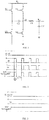
- FIG. 1 is a structural diagram of a buck-boost circuit according to an embodiment of the present disclosure. As shown in FIG. 1 , the buck-boost circuit includes a first switch S1, a second switch S2, a third switch S3, a fourth switch S4, a first inductor L1, a first capacitor C1, and a second capacitor C2.
- a first terminal of the first switch S1 is connected to an anode of an input power supply V BAT
- a first terminal of the second switch S2 is connected to the anode of the input power supply V BAT
- a first terminal of the third switch S3 and a first terminal of the first capacitor C1 are connected to a second terminal of the first switch S1
- a second terminal of the third switch S3 is connected to a cathode of the input power supply V BAT (for example, for grounding)
- a first terminal of the fourth switch S4 a second terminal of the first capacitor C1
- a first terminal of the first inductor L1 are connected to a second terminal of the second switch S2
- a second terminal of the fourth switch S4 is connected to the cathode of the input power supply V BAT (for example, for grounding)
- a second terminal of the first inductor L1 is connected to an anode of an output power supply V out
- the second capacitor C2 is connected in parallel between the anode and
- a control module can be provided to control a status of each switch based on a relationship between a target voltage V tar and an input voltage V BAT , to realize bucking and boosting modes of the circuit.
- the control module can be implemented in the buck-boost circuit, or can be independent from the buck-boost circuit, and can execute, according to a preset program or an external instruction, control methods provided in some embodiments of the present disclosure to control the switch.
- the switch not mentioned in the control methods is in an off state by default.
- a control method of the buck-boost circuit in FIG. 1 includes:
- ⁇ V represents the set voltage difference. It is defined as required, and for example, can be 100 mV, 200 mV, or the like.
- the first switch S1 and the third switch S3 are turned off, so that both S1 and S3 are in an off state, and the second switch S2 and the fourth switch S4 are complementarily tuned on.
- the second switch S2 is turned on, a voltage at LX is V BAT , and an inductive current of the first inductor L1 increases linearly.
- the second switch S2 is turned off and the fourth switch S4 is turned on, the voltage at the LX is 0. Because the inductive current cannot change suddenly, a circuit is formed through the fourth switch S4 to charge the second capacitor C2.
- Each switch has an initial state of an off state by default.
- V out (t on /T) ⁇ V BAT (1), where t on represents a turn-on time of the second switch, and t on /T represents a duty cycle of a control voltage of the second switch.
- V BAT V BAT + ⁇ V
- the circuit operates in a bypass mode.
- the first switch S1 and the third switch S3 are in the off state
- the second switch S2 is in a normally-open state (namely, the second switch S2 is in an ON state continuously)
- the fourth switch S4 is in a normally-closed state.
- the circuit When V tar >V BAT + ⁇ V, the circuit operates in a boosting mode.
- the fourth switch S4 is in the off state, the second switch S2 and the third switch S3 operate simultaneously, and the second switch S2 and the first switch S 1 are complementarily turned on, in other words, the third switch S3 and the first switch S 1 are also complementarily turned on.
- the second switch S2 and the third switch S3 When the second switch S2 and the third switch S3 are turned on, the voltage at LX is V BAT , and the inductive current of the first inductor L1 increases linearly.
- the second switch S2 and the third switch S3 are turned off, and the first switch S1 is turned on, the first inductor L1 charges the first capacitor C1 to enable the voltage at LX to reach 2V BAT .
- V OUT (1+t on /T) ⁇ V BAT (2).
- the buck-boost circuit in this embodiment can quickly boost the output voltage in the boosting mode.
- a voltage stabilization time can be reduced when the buck-boost circuit regulates the output voltage, and the voltage can be regulated quickly and stably.
- each switch provided in the embodiments of the present disclosure can be a semiconductor transistor, such as a bipolar transistor, a field effect transistor, or a switch of any other type.
- FIG. 5 is a structural diagram of a buck-boost circuit according to an embodiment of the present disclosure.
- the buck-boost circuit further includes a fifth switch S5.
- the fifth switch S5 is connected in series with the first capacitor C1, and is connected between the second terminal of the first capacitor C1 and the second terminal of the second switch, in other words, between being connected between the second terminal of the first capacitor C1 and the first terminal of the first inductor L1.
- an operation status of the buck-boost circuit is the same as that in FIG. 1 .
- S5 can be appropriately regulated based on an application scenario, so that the circuit can be applied more flexibly.
- a first control method of the buck-boost circuit in FIG. 5 includes:
- the circuit when V tar ⁇ V BAT ⁇ V, the circuit operates in a bucking mode.
- the fifth switch S5 is in the off state
- the second switch S2 and the fourth switch S4 are complementarily turned on
- the first switch S1 and the third switch S3 have opposite statuses or are both in an off state, in other words, S1 is turned on and S3 is turned off, S3 is turned on and S1 is turned off, or both S1 and S3 are turned off.
- the second switch S2 is turned on, the voltage at LX is V BAT , and the inductive current of the first inductor L1 increases linearly.
- the second switch S2 is turned off and the fourth switch S4 is turned on
- the voltage at LX is 0. Because the inductive current cannot change suddenly, the circuit is formed through the fourth switch S4 to charge the second capacitor C2.
- the circuit When V BAT ⁇ V ⁇ V tar ⁇ V BAT + ⁇ V, the circuit operates in a bucking and boosting mode, and a control method can be referred to FIG. 7 .
- the first switch S1 and the third switch S3 are complementarily turned on
- the fourth switch S4 and the fifth switch S5 are complementarily turned on
- the second switch S2 is turned on from turning off of the first switch S1 to turning on of the fourth switch S4.
- the circuit When V tar >V BAT + ⁇ V, the circuit operates in the boosting mode.
- the fifth switch S5 is turned on
- the fourth switch S4 is turned off
- the second switch S2 and the third switch S3 operates simultaneously
- the second switch S2 and the first switch S1 are complementarily turned on.
- the operation mode is the same as the boosting mode in FIG. 1 .
- a second control method of the buck-boost circuit in FIG. 5 includes:
- the control method is different from the first control method only when V BAT ⁇ ⁇ V ⁇ V tar ⁇ V BAT + ⁇ V.
- the circuit When V BAT ⁇ V ⁇ V tar ⁇ V BAT + ⁇ V, the circuit operates in a bucking and boosting mode.
- a control method can be referred to FIG. 9 .
- the first switch S1 and the third switch S3 are complementarily turned on
- the fourth switch S4 and the fifth switch S5 are complementarily turned on
- the second switch S2 is turned on from turning-off of the fourth switch S4 to turning-on of the first switch S1.
- the fourth switch S4 When the fourth switch S4 is turned on, the voltage at LX is 0.
- the fourth switch S4 When the fourth switch S4 is turned off and the second switch S2 is turned on, the voltage at LX is V BAT , and a turning-on time of the second switch S2 is t on2 .
- the voltage at LX is 2V BAT , and a turning-on time of the first switch S1 is t on1 .
- a desired output voltage is obtained by controlling t on1 and t on2 .
- the calculation formula of the output voltage is the same as the formula (3).
- FIG. 10 is a structural diagram of a buck-boost circuit according to an embodiment of the present disclosure. As shown in FIG. 10 , compared with the buck-boost circuit in FIG. 1 , the buck-boost circuit further includes a sixth switch S6.
- the sixth switch S6 is connected in parallel to the first capacitor C1, and is connected between the second terminal of the first switch S1 and the first terminal of the first inductor.
- a control method of the buck-boost circuit in FIG. 10 includes:
- the circuit when V tar ⁇ V BAT ⁇ V, the circuit operates in the bucking mode.
- the sixth switch S6 is turned on, the first switch S1 and the second switch S2 operate simultaneously, the third switch S3 and the fourth switch S4 operate simultaneously, and the first switch S1 and the third switch S3 are complementarily turned on.
- the voltage at LX is V BAT .
- the first switch S1 and the second switch S2 are turned off, and the third switch and the fourth switch S4 are turned on, the voltage at LX is 0.
- the circuit When V BAT ⁇ V ⁇ V tar ⁇ V BAT + ⁇ V, the circuit operates in the bypass mode. Referring to a switch status diagram shown in FIG. 12 , the first switch S1, the third switch S3, and the fourth switch S4 are turned off, and the second switch S2 and the sixth switch S6 are turned on.
- the circuit When V tar >V BAT + ⁇ V, the circuit operates in the boosting mode.
- the fourth switch S4 and the sixth switch S6 are turned off, the second switch S2 and the third switch S3 operate simultaneously, and the second switch S2 and the first switch S1 are complementarily turned on.
- the voltage at LX is 2V BAT .
- the sixth switch is in the normally-closed state, which is the same as that in the boosting mode in FIG. 1 .
- FIG. 14 is a structural diagram of a buck-boost circuit according to an embodiment of the present disclosure. As shown in FIG. 14 , compared with the buck-boost circuit in FIG. 1 , the buck-boost circuit further includes a seventh switch S7.
- the seventh switch S7 is connected in parallel with the first inductor L1, and is connected between the second terminal of the second switch S1 and the anode of the output power supply.
- the circuit When the seventh switch S7 is in the normally-closed state, the circuit is the same as that in FIG. 1 .
- the seventh switch S7 When the output voltage of the circuit is required to be regulated, the seventh switch S7 is turned on to charge or discharge the output capacitor quickly, so that the output voltage can be quickly regulated to the target voltage.
- the control module controls the switches based on the relationship between the output voltage V out and the target voltage V tar and the relationship between the target voltage V tar and the input voltage V BAT , and such controlling includes:
- the first operation mode includes:
- FIG. 15 shows an output voltage and a switch status in a boosting process of the buck-boost circuit in this embodiment.
- V out ⁇ V tar ⁇ V and V tar ⁇ V BAT as represented by the first half of an output voltage curve in FIG. 15 , the circuit is essentially a bucking circuit, and the actual output voltage is smaller than the target voltage, and needs to be boosted to reach the target voltage, in other words, the output voltage is in a boosting state.
- the supply voltage V BAT is higher than the output voltage.
- the fourth switch S4 is turned off, and the second switch S2 and the seventh switch S7 are turned on to quickly charge the second capacitor C2 connected to the output terminal of the buck-boost circuit.
- the output voltage is boosted quickly.
- the seventh switch S7 is turned off to stop quick charging.
- the circuit is restored to the structure in FIG. 1 , and enters a control process of the buck-boost circuit in FIG. 1 , in other words, entering the first operation mode.
- the output voltage is gradually regulated to the target voltage V tar , and V tar is stably output.
- the circuit is essentially a boosting circuit, and the actual output voltage needs to be boosted to reach the target voltage, in other words, the output voltage is in the boosting state.
- the second switch S2, the third switch S3, and the seventh switch S7 are turned on.
- the second switch S2 and the third switch S3 are turned off, and the first switch S1 is turned on to continue to quickly charge the second capacitor C2 through the first capacitor C1.
- the first switch S1 and the seventh switch S7 are turned off.
- the circuit is restored to the structure in FIG. 1 , and enters the control process of the buck-boost circuit in FIG. 1 , in other words, entering the first operation mode.
- FIG. 16 shows an output voltage and a switch status in a bucking process of the buck-boost circuit in this embodiment.
- V out >V tar + ⁇ V as represented by an output voltage curve in FIG. 16 , the actual output voltage is greater than the target voltage, and needs to be bucked to reach the target voltage, in other words, the output voltage is in a bucking state.
- the seventh switch S7 and the fourth switch S4 are turned on to discharge the second capacitor C2 connected to the output terminal.
- the seventh switch S7 and the fourth switch S4 are turned off.
- the circuit is restored to the structure in FIG. 1 , and enters the control process of the buck-boost circuit in FIG. 1 , in other words, entering the first operation mode.
- FIG. 17 is a structural diagram of a buck-boost circuit according to an embodiment of the present disclosure. As shown in FIG. 17 , compared with the buck-boost circuit in FIG. 5 , the buck-boost circuit further includes a seventh switch S7.
- the seventh switch S7 is connected in parallel with the first inductor L1, and is connected between the second terminal of the second switch S1 and the anode of the output power supply.
- the circuit When the seventh switch S7 is in the normally-closed state, the circuit is the same as that in FIG. 5 .
- FIG. 19 is a structural diagram of a buck-boost circuit according to an embodiment of the present disclosure. As shown in FIG. 19 , compared with the buck-boost circuit in FIG. 10 , the buck-boost circuit further includes a seventh switch S7.
- the seventh switch S7 is connected in parallel with the first inductor L1, and is connected between the second terminal of the second switch S1 and the anode of the output power supply.
- the circuit When the seventh switch S7 is in the normally-closed state, the circuit is the same as that in FIG. 10 .
- control methods of the fourth switch S4 and the seventh switch S7 are the same as those in the bucking process of the buck-boost circuit in FIG. 14 .
Landscapes
- Engineering & Computer Science (AREA)
- Power Engineering (AREA)
- Dc-Dc Converters (AREA)
Abstract
Description
- The present disclosure relates to the field of direct current conversion, and in particular, to a buck-boost circuit and a control method thereof.
- A buck-boost circuit can effectively reduce system power consumption by regulating an output voltage. With the starting of the age of 5G communication, a circuit capable of boosting and bucking a voltage quickly is needed to ensure a smooth communication and facilitate reduction of the system power consumption.
- The existing buck-boost structure takes a too long time to realize buck-boost switching. As a result, a voltage stabilization time is relatively long when regulating the output voltage, especially when switching from a bucking mode to a boosting mode, an intermediate switching process is time-consuming, and thus the voltage stabilization time is too long to meet a communication requirement of a system, which reduces signal sensitivity when using the system, thereby causing a communication failure.
- Therefore, how to reduce the voltage stabilization time of the buck-boost circuit during voltage regulation and regulate the voltage quickly has become a big problem to be solved.
- In view of the above, the present disclosure provides a buck-boost circuit and a control method thereof, so that a voltage can be regulated quickly and stably.
- According to an aspect of the present disclosure, a buck-boost circuit is provided. The buck-boost circuit includes a first switch, a second switch, a third switch, a fourth switch, a first inductor, a first capacitor, and a second capacitor. A first terminal of the first switch is connected to an anode of an input power supply. A first terminal of the second switch is connected to the anode of the input power supply. A first terminal of the third switch and a first terminal of the first capacitor are connected to a second terminal of the first switch. A second terminal of the third switch is connected to a cathode of the input power supply. A first terminal of the fourth switch, a second terminal of the first capacitor, and a first terminal of the first inductor are connected to a second terminal of the second switch. A second terminal of the fourth switch is connected to the cathode of the input power supply. A second terminal of the first inductor is connected to an anode of an output power supply. The second capacitor is connected in parallel between the anode and a cathode of the output power supply
- In an embodiment, the buck-boost circuit further includes a fifth switch connected between the second terminal of the first capacitor and the second terminal of the second switch.
- In an embodiment, the buck-boost circuit further includes a sixth switch connected in parallel with the first capacitor.
- In an embodiment, the buck-boost circuit further includes a seventh switch connected in parallel with the first inductor.
- In an embodiment, the buck-boost circuit further includes a control module configured to control switches based on a relationship between a target voltage Vtar and an input voltage VBAT, and the controlling the switches includes:
- in response to Vtar<VBAT―ΔV being satisfied, turning off the first switch and the third switch, and complementarily turning on the second switch and the fourth switch, where ΔV denotes a set voltage difference;
- in response to VBAT―ΔV≤Vtar≤VBAT+ΔV being satisfied, turning off the first switch, the third switch, and the fourth switch, and turning on the second switch; and
- in response to Vtar>VBAT+ΔV being satisfied, turning off the fourth switch, enabling both the second switch and the third switch to operate simultaneously, and complementarily turning on the second switch and the first switch.
- In an embodiment, the buck-boost circuit further includes a control module configured to control switches based on a relationship between a target voltage Vtar and an input voltage VBAT, and the controlling the switches includes:
- in response to Vtar<VBAT―ΔV being satisfied, turning off the fifth switch, enabling the first switch and the third switch to be in opposite states or to be both in an off state, and complementarily turning on the second switch and the fourth switch, where ΔV denotes a set voltage difference;
- in response to VBAT―ΔV≤Vtar≤VBAT+ΔV being satisfied, complementarily turning on the first switch and the third switch, complementarily turning on the fourth switch and the fifth switch, and turning on the second switch from turning-off of the first switch to turning-on of the fourth switch; and
- in response to Vtar>VBAT+ΔV being satisfied, turning on the fifth switch, turning off the fourth switch, enabling both the second switch and the third switch to operate simultaneously, and complementarily turning on the second switch and the first switch.
- In an embodiment, the buck-boost circuit further includes a control module configured to control switches based on a relationship between a target voltage Vtar and an input voltage VBAT, and the controlling the switches includes:
- in response to Vtar<VBAT―ΔV being satisfied, turning off the fifth switch, enabling the first switch and the third switch to be in opposite states or to be both in an off state, and complementarily turning on the second switch and the fourth switch, where ΔV denotes a set voltage difference;
- in response to VBAT―ΔV≤Vtar≤VBAT+ΔV being satisfied, complementarily turning on the first switch and the third switch, complementarily turning on the fourth switch and the fifth switch, and truing on the second switch from turning-off of the fourth switch to truing-on of the first switch; and
- in response to Vtar>VBAT+ΔV being satisfied, turning on the fifth switch, turning off the fourth switch, enabling the second switch and the third switch to operate simultaneously, and complementarily turning on the second switch and the first switch.
- In an embodiment, the buck-boost circuit further includes a control module configured to control switches based on a relationship between a target voltage Vtar and an input voltage VBAT, and the controlling the switches includes:
- in response to Vtar<VBAT―ΔV being satisfied, turning on the sixth switch, enabling the first switch and the second switch to simultaneously operate, enabling the third switch and the fourth switch to simultaneously operate, and complementarily turning on the first switch and the third switch, where ΔV denotes a set voltage difference;
- in response to VBAT―ΔV≤Vtar≤VBAT+ΔV being satisfied, turning off the first switch, the third switch, and the fourth switch, and turning on the second switch and the sixth switch; and
- in response to Vtar>VBAT+ΔV being satisfied, turning off the fourth switch and the sixth switch, enabling the second switch and the third switch to operate simultaneously, and complementarily turning on the second switch and the first switch.
- In an embodiment, the buck-boost circuit further includes a control module configured to control switches based on a relationship between an output voltage Vout and a target voltage Vtar and a relationship between the target voltage Vtar and an input voltage VBAT, and the controlling the switches includes:
- in response to Vout<Vtar―ΔV and Vtar≤VBAT being satisfied, turning off the fourth switch, and turning on the second switch and the seventh switch to charge the second capacitor connected to an output terminal of the buck-boost circuit; and turning off the seventh switch to enter a first operation mode in response to Vout=Vtar―ΔV being satisfied, where ΔV denotes a set voltage difference;
- turning on the second switch, the third switch, and the seventh switch to charge the second capacitor in response to both Vout<Vtar―ΔV and Vtar>VBAT being satisfied; in response to Vout=VBAT being satisfied, turning off the second switch and the third switch, and simultaneously turning on the first switch to charge the second capacitor through the first capacitor; and turning off the first switch and the seventh switch to enter the first operation mode in response to Vout=Vtar―ΔV being satisfied;
- turning on the seventh switch and the fourth switch to perform discharging in response to Vout>Vtar+ΔV being satisfied, and turning off the seventh switch and the fourth switch to enter the first operation mode in response to Vout=Vtar+ΔV being satisfied; and
- entering the first operation mode in response to Vtar―ΔV≤Vout≤Vtar+ΔV being satisfied; and
- the first operation mode includes:
- in response to Vtar<VBAT―ΔV being satisfied, turning off the first switch and the third switch, and complementarily turning on the second switch and the fourth switch, where ΔV denotes the set voltage difference;
- in response to VBAT―ΔV≤Vtar≤VBAT+ΔV being satisfied, turning off the first switch, the third switch, and the fourth switch, and turning on the second switch; and
- in response to Vtar>VBAT+ΔV being satisfied, turning off the fourth switch, enabling the second switch and the third switch to operate simultaneously, and complementarily turning on the second switch and the first switch.
- In an embodiment, the control module is further configured to turn on the fifth switch in response to both Vout<Vtar―ΔV and Vtar>VBAT being satisfied and to turn off the fifth switch in response to Vout=VBAT being satisfied.
- In an embodiment, the control module is further configured to turn on the sixth switch and the third switch to perform in response to Vout>Vtar+ΔV being satisfied and to turn off the sixth switch and the third switch in response to Vout=Vtar+ΔV being satisfied.
- Twice an input supply voltage is generated on one terminal of the inductor when the capacitor and the switch work cooperate to operate, so that the buck-boost circuit in the present disclosure can quickly boost an output voltage in a boosting mode. In this way, a voltage stabilization time can be reduced when the buck-boost circuit regulates the output voltage, and the voltage are regulated quickly and stably.
- According to the following detailed description of exemplary embodiments with reference to the accompanying drawings, other features and aspects of the present disclosure will become clear.
- The accompanying drawings included in this specification and constituting a part of this specification, together with this specification, illustrate exemplary embodiments, features, and aspects of the present disclosure, and are used to explain the principle of the present disclosure.
-
FIG. 1 is a structural diagram of a buck-boost circuit according to an embodiment of the present disclosure; -
FIG. 2 shows a switch status of the buck-boost circuit inFIG. 1 in a bucking mode, and a voltage at a point LX; -
FIG. 3 shows a switch status of the buck-boost circuit inFIG. 1 in a bypass mode, and a voltage at a point LX; -
FIG. 4 shows a switch status of the buck-boost circuit inFIG. 1 in a boosting mode, and a voltage at a point LX; -
FIG. 5 is a structural diagram of a buck-boost circuit according to an embodiment of the present disclosure; -
FIG. 6 shows a switch status of the buck-boost circuit inFIG. 5 in a bucking mode, and a voltage at a point LX; -
FIG. 7 shows a switch status of the buck-boost circuit inFIG. 5 in a bucking and boosting mode, and a voltage at a point LX; -
FIG. 8 shows a switch status of the buck-boost circuit inFIG. 5 in a boosting mode, and a voltage at a point LX; -
FIG. 9 shows another switch status of the buck-boost circuit inFIG. 5 in a bucking and boosting mode, and a voltage at a point LX; -
FIG. 10 is a structural diagram of a buck-boost circuit according to an embodiment of the present disclosure; -
FIG. 11 shows a switch status of the buck-boost circuit inFIG. 10 in a bucking mode, and a voltage at a point LX; -
FIG. 12 shows a switch status of the buck-boost circuit inFIG. 10 in a bypass mode, and a voltage at a point LX; -
FIG. 13 shows a switch status of the buck-boost circuit inFIG. 10 in a boosting mode, and a voltage at a point LX; -
FIG. 14 is a structural diagram of a buck-boost circuit according to an embodiment of the present disclosure; -
FIG. 15 shows an output voltage and a switch status in a boosting process of the buck-boost circuit inFIG. 14 ; -
FIG. 16 shows an output voltage and a switch status in a bucking process of the buck-boost circuit inFIG. 14 ; -
FIG. 17 is a structural diagram of a buck-boost circuit according to an embodiment of the present disclosure; -
FIG. 18 shows an output voltage and a switch status in a boosting process of the buck-boost circuit inFIG. 17 ; -
FIG. 19 is a structural diagram of a buck-boost circuit according to an embodiment of the present disclosure; and -
FIG. 20 shows an output voltage and a switch status in a bucking process of the buck-boost circuit inFIG. 19 . - Various exemplary embodiments, features, and aspects of the present disclosure will be described in detail below with reference to the accompanying drawings. The same reference numerals in the accompanying drawings indicate elements with the same or similar functions. Although various aspects of the embodiments are shown in the accompanying drawings, unless otherwise noted, the accompanying drawings are not necessarily drawn to scale.
- The dedicated word "exemplary" herein means "serving as an example, embodiment, or illustration". Any embodiment described herein as "exemplary" need not be construed as being superior to or better than other embodiments.
- In addition, to better illustrate the present disclosure, numerous specific details are given in the following specific implementations. Those skilled in the art should understand that the present disclosure can also be implemented without certain specific details. In some examples, the methods, means, elements, and circuits well-known to those skilled in the art are not described in detail in order to highlight the subject matter of the present disclosure.
-
FIG. 1 is a structural diagram of a buck-boost circuit according to an embodiment of the present disclosure. As shown inFIG. 1 , the buck-boost circuit includes a first switch S1, a second switch S2, a third switch S3, a fourth switch S4, a first inductor L1, a first capacitor C1, and a second capacitor C2. - A first terminal of the first switch S1 is connected to an anode of an input power supply VBAT, a first terminal of the second switch S2 is connected to the anode of the input power supply VBAT, a first terminal of the third switch S3 and a first terminal of the first capacitor C1 are connected to a second terminal of the first switch S1, a second terminal of the third switch S3 is connected to a cathode of the input power supply VBAT (for example, for grounding), a first terminal of the fourth switch S4, a second terminal of the first capacitor C1, and a first terminal of the first inductor L1 are connected to a second terminal of the second switch S2, a second terminal of the fourth switch S4 is connected to the cathode of the input power supply VBAT (for example, for grounding), a second terminal of the first inductor L1 is connected to an anode of an output power supply Vout, and the second capacitor C2 is connected in parallel between the anode and a cathode of the output power supply Vout.
- A control module can be provided to control a status of each switch based on a relationship between a target voltage Vtar and an input voltage VBAT, to realize bucking and boosting modes of the circuit. The control module can be implemented in the buck-boost circuit, or can be independent from the buck-boost circuit, and can execute, according to a preset program or an external instruction, control methods provided in some embodiments of the present disclosure to control the switch. The switch not mentioned in the control methods is in an off state by default.
- A control method of the buck-boost circuit in
FIG. 1 includes: - when Vtar<VBAT―ΔV, turning off the first switch S1 and the third switch S3, and complementarily turning on the second switch S2 and the fourth switch S4, where ΔV represents a set voltage difference;
- when VBAT―ΔV≤Vtar≤VBAT+ΔV, turning off the first switch S1, the third switch S3, and the fourth switch S4, and turning on the second switch S2; or
- when Vtar>VBAT+ΔV, turning off the fourth switch S4, enabling the second switch S2 and the third switch S3 to operate simultaneously, and complementarily turning on the second switch S2 and the first switch S1.
- In other words, when Vtar<VBAT―ΔV, the circuit operates in the bucking mode. ΔV represents the set voltage difference. It is defined as required, and for example, can be 100 mV, 200 mV, or the like. Referring to a switch status diagram shown in
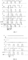
FIG. 2 , the first switch S1 and the third switch S3 are turned off, so that both S1 and S3 are in an off state, and the second switch S2 and the fourth switch S4 are complementarily tuned on. When the second switch S2 is turned on, a voltage at LX is VBAT, and an inductive current of the first inductor L1 increases linearly. When the second switch S2 is turned off and the fourth switch S4 is turned on, the voltage at the LX is 0. Because the inductive current cannot change suddenly, a circuit is formed through the fourth switch S4 to charge the second capacitor C2. Each switch has an initial state of an off state by default. - According to the volt-second principle, it can be learned that a calculation formula of an output voltage is: Vout=(ton/T)×VBAT (1), where ton represents a turn-on time of the second switch, and ton/T represents a duty cycle of a control voltage of the second switch.
- When VBAT―ΔV ≤Vtar≤VBAT+ΔV, the circuit operates in a bypass mode. Referring to a switch status diagram shown in
FIG. 3 , the first switch S1 and the third switch S3 are in the off state, the second switch S2 is in a normally-open state (namely, the second switch S2 is in an ON state continuously), and the fourth switch S4 is in a normally-closed state. The second switch S4 is always turned on, and the voltage at LX is always VBAT. Therefore, Vout=VBAT. - When Vtar>VBAT+ΔV, the circuit operates in a boosting mode. Referring to a switch status diagram shown in
FIG. 4 , the fourth switch S4 is in the off state, the second switch S2 and the third switch S3 operate simultaneously, and the second switch S2 and thefirst switch S 1 are complementarily turned on, in other words, the third switch S3 and thefirst switch S 1 are also complementarily turned on. When the second switch S2 and the third switch S3 are turned on, the voltage at LX is VBAT, and the inductive current of the first inductor L1 increases linearly. When the second switch S2 and the third switch S3 are turned off, and the first switch S1 is turned on, the first inductor L1 charges the first capacitor C1 to enable the voltage at LX to reach 2VBAT. - According to the volt-second principle, it can be learned that the calculation formula of the output voltage is: VOUT=(1+ton/T)×VBAT (2).
- Twice the input supply voltage is generated on one terminal of the inductor when the capacitor and the switch cooperate to operate, so that the buck-boost circuit in this embodiment can quickly boost the output voltage in the boosting mode. In this way, a voltage stabilization time can be reduced when the buck-boost circuit regulates the output voltage, and the voltage can be regulated quickly and stably.
- It should be noted that each switch provided in the embodiments of the present disclosure can be a semiconductor transistor, such as a bipolar transistor, a field effect transistor, or a switch of any other type.
-
FIG. 5 is a structural diagram of a buck-boost circuit according to an embodiment of the present disclosure. As shown inFIG. 5 , compared with the buck-boost circuit inFIG. 1 , the buck-boost circuit further includes a fifth switch S5. The fifth switch S5 is connected in series with the first capacitor C1, and is connected between the second terminal of the first capacitor C1 and the second terminal of the second switch, in other words, between being connected between the second terminal of the first capacitor C1 and the first terminal of the first inductor L1. - When the fifth switch S5 is in the normally-open state, an operation status of the buck-boost circuit is the same as that in
FIG. 1 . S5 can be appropriately regulated based on an application scenario, so that the circuit can be applied more flexibly. - A first control method of the buck-boost circuit in
FIG. 5 includes: - when Vtar<VBAT―ΔV, turning off the fifth switch S5, enabling the first switch S1 and the third switch S3 to be in opposite states or to be both in the off state, and complementarily turning on the second switch S2 and the fourth switch S4, where ΔV represents the set voltage difference;
- when VBAT―ΔV≤Vtar≤VBAT+ΔV, complementarily turning on the first switch S1 and the third switch S3, complementarily turning on the fourth switch S4 and the fifth switch S5, and enabling the second switch S2 to be switched on from turning-off of the first switch S1 to turning-on of the fourth switch S4; and
- when Vtar>VBAT+ΔV, turning on the fifth switch S5, turning off the fourth switch S4, enabling the second switch S2 and the third switch S3 to operate simultaneously, and complementarily turning on the second switch S2 and the first switch S1.
- In other words, when Vtar<VBAT―ΔV, the circuit operates in a bucking mode. Referring to a switch status diagram shown in
FIG. 6 , the fifth switch S5 is in the off state, the second switch S2 and the fourth switch S4 are complementarily turned on, and the first switch S1 and the third switch S3 have opposite statuses or are both in an off state, in other words, S1 is turned on and S3 is turned off, S3 is turned on and S1 is turned off, or both S1 and S3 are turned off. When the second switch S2 is turned on, the voltage at LX is VBAT, and the inductive current of the first inductor L1 increases linearly. When the second switch S2 is turned off and the fourth switch S4 is turned on, the voltage at LX is 0. Because the inductive current cannot change suddenly, the circuit is formed through the fourth switch S4 to charge the second capacitor C2. - When VBAT―ΔV ≤Vtar≤VBAT+ΔV, the circuit operates in a bucking and boosting mode, and a control method can be referred to
FIG. 7 . The first switch S1 and the third switch S3 are complementarily turned on, the fourth switch S4 and the fifth switch S5 are complementarily turned on, and the second switch S2 is turned on from turning off of the first switch S1 to turning on of the fourth switch S4. When both the first switch S1 and the fifth switch S5 are turned on, the voltage at LX is 2VBAT, and a turn-on time of the first switch S1 is ton1, in other words, a time during which both the first switch S1 and the fifth switch S5 are turned on is ton1. When the first switch S1 is turned off and the second switch S2 is turned on, the voltage at LX is VBAT, and a turn-on time of the second switch S2 is ton2. When the fourth switch S4 is turned on, the voltage at LX is 0. A desired output voltage is obtained by controlling ton1 and ton2. The calculation formula of the output voltage is:
- When Vtar>VBAT+ΔV, the circuit operates in the boosting mode. Referring to a switch status diagram shown in
FIG. 8 , the fifth switch S5 is turned on, the fourth switch S4 is turned off, the second switch S2 and the third switch S3 operates simultaneously, and the second switch S2 and the first switch S1 are complementarily turned on. The operation mode is the same as the boosting mode inFIG. 1 . - A second control method of the buck-boost circuit in
FIG. 5 includes: - when Vtar≤VBAT―ΔV, turning off the fifth switch S5, enabling the first switch S1 and the third switch S3 to be in opposite states or to be both in the off state, and complementarily turning on the second switch S2 and the fourth switch S4, where ΔV represents the set voltage difference;
- when VBAT―ΔV≤Vtar≤VBAT+ΔV, complementarily turning on the first switch S1 and the third switch S3, complementarily turning on the fourth switch S4 and the fifth switch S5, and turning on the second switch S2 from turning-off of the fourth switch S4 to turning-on of the first switch S1; and
- when Vtar>VBAT+ΔV, turning on the fifth switch S5, turning off the fourth switch S4, enabling both the second switch S2 and the third switch S3 to operate simultaneously, and complementarily turning on the second switch S2 and the first switch S1.
- The control method is different from the first control method only when VBAT― ΔV≤Vtar≤VBAT+ΔV.
- When VBAT―ΔV ≤Vtar≤VBAT+ΔV, the circuit operates in a bucking and boosting mode. A control method can be referred to
FIG. 9 . The first switch S1 and the third switch S3 are complementarily turned on, the fourth switch S4 and the fifth switch S5 are complementarily turned on, and the second switch S2 is turned on from turning-off of the fourth switch S4 to turning-on of the first switch S1. When the fourth switch S4 is turned on, the voltage at LX is 0. When the fourth switch S4 is turned off and the second switch S2 is turned on, the voltage at LX is VBAT, and a turning-on time of the second switch S2 is ton2. When the first switch S1 is turned on, the voltage at LX is 2VBAT, and a turning-on time of the first switch S1 is ton1. Similarly, a desired output voltage is obtained by controlling ton1 and ton2. The calculation formula of the output voltage is the same as the formula (3). -
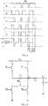
FIG. 10 is a structural diagram of a buck-boost circuit according to an embodiment of the present disclosure. As shown inFIG. 10 , compared with the buck-boost circuit inFIG. 1 , the buck-boost circuit further includes a sixth switch S6. The sixth switch S6 is connected in parallel to the first capacitor C1, and is connected between the second terminal of the first switch S1 and the first terminal of the first inductor. - When the sixth switch S6 is in the normally-closed state (in other words, is always turned off), an operation status of the buck-boost circuit is the same as that in
FIG. 1 . - A control method of the buck-boost circuit in
FIG. 10 includes: - when Vtar<VBAT―ΔV, turning on the sixth switch S6, enabling both the first switch S1 and the second switch S2 to operate simultaneously, enabling both the third switch S3 and the fourth switch S4 to operate simultaneously, and complementarily turning on the first switch S1 and the third switch S3 to be in complementary control, where ΔV represents the set voltage difference;
- when VBAT―ΔV≤Vtar≤VBAT+ΔV, turning off the first switch S1, the third switch S3, and the fourth switch S4, and turning on the second switch S2 and the sixth switch S6; and
- when Vtar>VBAT+ΔV, turning off the fourth switch S4 and the sixth switch S6, enabling both the second switch S2 and the third switch S3 to operate simultaneously, and complementarily turning on the second switch S2 and the first switch S1.
- In other words, when Vtar<VBAT―ΔV, the circuit operates in the bucking mode. Referring to a switch status diagram shown in
FIG. 11 , the sixth switch S6 is turned on, the first switch S1 and the second switch S2 operate simultaneously, the third switch S3 and the fourth switch S4 operate simultaneously, and the first switch S1 and the third switch S3 are complementarily turned on. When the first switch S1 and the second switch S2 are turned on, the voltage at LX is VBAT. When the first switch S1 and the second switch S2 are turned off, and the third switch and the fourth switch S4 are turned on, the voltage at LX is 0. - When VBAT―ΔV ≤Vtar≤VBAT+ΔV, the circuit operates in the bypass mode. Referring to a switch status diagram shown in
FIG. 12 , the first switch S1, the third switch S3, and the fourth switch S4 are turned off, and the second switch S2 and the sixth switch S6 are turned on. - When Vtar>VBAT+ΔV, the circuit operates in the boosting mode. Referring to a switch status diagram shown in
FIG. 13 , the fourth switch S4 and the sixth switch S6 are turned off, the second switch S2 and the third switch S3 operate simultaneously, and the second switch S2 and the first switch S1 are complementarily turned on. When the first switch S1 is turned on, the voltage at LX is 2VBAT. When the first switch S1 is turned off, and the second switch S2 and the third switch S3 are turned on, the voltage at LX is VBAT. In other words, the sixth switch is in the normally-closed state, which is the same as that in the boosting mode inFIG. 1 . -
FIG. 14 is a structural diagram of a buck-boost circuit according to an embodiment of the present disclosure. As shown inFIG. 14 , compared with the buck-boost circuit inFIG. 1 , the buck-boost circuit further includes a seventh switch S7. The seventh switch S7 is connected in parallel with the first inductor L1, and is connected between the second terminal of the second switch S1 and the anode of the output power supply. - When the seventh switch S7 is in the normally-closed state, the circuit is the same as that in
FIG. 1 . When the output voltage of the circuit is required to be regulated, the seventh switch S7 is turned on to charge or discharge the output capacitor quickly, so that the output voltage can be quickly regulated to the target voltage. - The control module controls the switches based on the relationship between the output voltage Vout and the target voltage Vtar and the relationship between the target voltage Vtar and the input voltage VBAT, and such controlling includes:
- when Vout<Vtar―ΔV and Vtar≤VBAT, turning off the fourth switch S4, and turning on the second switch S2 and the seventh switch S7 to charge the second capacitor C2 connected to an output terminal of the buck-boost circuit; and when Vout=Vtar―ΔV, turning off the seventh switch S7 to enter the first operation mode, where ΔV represents the set voltage difference;
- when Vout<Vtar―ΔV and Vtar≤VBAT, turning on the second switch S2, the third switch S3, and the seventh switch S7 to charge the second capacitor C2; when Vout=Vtar―ΔV, turning off the second switch S2 and the third switch S3, and turning on the first switch S1 to charge the second capacitor C2 through the first capacitor C1; and when Vout=Vtar―ΔV, turning off the first switch S1 and the seventh switch S7 to enter the first operation mode;
- when Vout>Vtar+ΔV, turning on the seventh switch S7 and the fourth switch S4 to perform discharging, and when Vout=Vtar+ΔV, turning off the seventh switch S7 and the fourth switch S4 to enter the first operation mode; and
- when Vtar―ΔV≤Vout≤Vtar+ΔV, entering the first operation mode.
- The first operation mode includes:
- when Vtar<VBAT―ΔV, truing off the first switch S1 and the third switch S3, and complementarily turning on the second switch S2 and the fourth switch S4, where ΔV represents the set voltage difference;
- when VBAT―ΔV≤Vtar≤VBAT+ΔV, turning off the first switch S1, the third switch S3, and the fourth switch S4, and turning on the second switch S2; and
- when Vtar>VBAT+ΔV, turning off the fourth switch S4, enabling the second switch S2 and the third switch S3 to operate simultaneously, and complementarily turning on the second switch S2 and the first switch.
-
FIG. 15 shows an output voltage and a switch status in a boosting process of the buck-boost circuit in this embodiment. When Vout<Vtar―ΔV and Vtar≤VBAT, as represented by the first half of an output voltage curve inFIG. 15 , the circuit is essentially a bucking circuit, and the actual output voltage is smaller than the target voltage, and needs to be boosted to reach the target voltage, in other words, the output voltage is in a boosting state. - At an initial stage, the supply voltage VBAT is higher than the output voltage. Firstly, the fourth switch S4 is turned off, and the second switch S2 and the seventh switch S7 are turned on to quickly charge the second capacitor C2 connected to the output terminal of the buck-boost circuit. The output voltage is boosted quickly. When the output voltage is smaller than the target voltage by ΔV, namely, Vout=Vtar―ΔV, the seventh switch S7 is turned off to stop quick charging. The circuit is restored to the structure in
FIG. 1 , and enters a control process of the buck-boost circuit inFIG. 1 , in other words, entering the first operation mode. The output voltage is gradually regulated to the target voltage Vtar, and Vtar is stably output. - When Vtar>VBAT, as represented by the last half of the output voltage curve in
FIG. 15 , the circuit is essentially a boosting circuit, and the actual output voltage needs to be boosted to reach the target voltage, in other words, the output voltage is in the boosting state. Firstly, the second switch S2, the third switch S3, and the seventh switch S7 are turned on. When the output voltage reaches VBAT, the second switch S2 and the third switch S3 are turned off, and the first switch S1 is turned on to continue to quickly charge the second capacitor C2 through the first capacitor C1. When the output voltage is smaller than the target voltage by ΔV, the first switch S1 and the seventh switch S7 are turned off. The circuit is restored to the structure inFIG. 1 , and enters the control process of the buck-boost circuit inFIG. 1 , in other words, entering the first operation mode. -
FIG. 16 shows an output voltage and a switch status in a bucking process of the buck-boost circuit in this embodiment. When Vout>Vtar+ΔV, as represented by an output voltage curve inFIG. 16 , the actual output voltage is greater than the target voltage, and needs to be bucked to reach the target voltage, in other words, the output voltage is in a bucking state. - Firstly, the seventh switch S7 and the fourth switch S4 are turned on to discharge the second capacitor C2 connected to the output terminal. When the voltage is greater than the target voltage by ΔV, namely, Vout=Vtar+ΔV, the seventh switch S7 and the fourth switch S4 are turned off. The circuit is restored to the structure in
FIG. 1 , and enters the control process of the buck-boost circuit inFIG. 1 , in other words, entering the first operation mode. -
FIG. 17 is a structural diagram of a buck-boost circuit according to an embodiment of the present disclosure. As shown inFIG. 17 , compared with the buck-boost circuit inFIG. 5 , the buck-boost circuit further includes a seventh switch S7. The seventh switch S7 is connected in parallel with the first inductor L1, and is connected between the second terminal of the second switch S1 and the anode of the output power supply. - When the seventh switch S7 is in the normally-closed state, the circuit is the same as that in
FIG. 5 . When the fifth switch S7 is in the normally-open state, the operation status is similar to that of the buck-boost circuit inFIG. 14 , and a difference is that the control module is further configured to turn on the fifth switch S5 when Vout<Vtar―ΔV and Vtar>VBAT, and to turn off the fifth switch S5 when Vout=VBAT. - In other words, in a boosting process, when Vout>VBAT, the fifth switch S5 needs to be turned on. A control method is shown in
FIG. 18 . Control methods of the first switch S1, the second switch S2, the third switch S3, and the seventh switch S7 are the same as those in the boosting process of the buck-boost circuit inFIG. 14 . -
FIG. 19 is a structural diagram of a buck-boost circuit according to an embodiment of the present disclosure. As shown inFIG. 19 , compared with the buck-boost circuit inFIG. 10 , the buck-boost circuit further includes a seventh switch S7. The seventh switch S7 is connected in parallel with the first inductor L1, and is connected between the second terminal of the second switch S1 and the anode of the output power supply. - When the seventh switch S7 is in the normally-closed state, the circuit is the same as that in
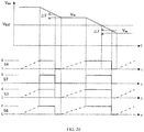
FIG. 10 . When the sixth switch S6 is in the off state, the operation status is similar to that of the buck-boost circuit inFIG. 14 , and a difference is that the control module is further configured to turn on the sixth switch S6 and the third switch S3 to perform discharging when Vout>Vtar+ΔV, and to turn off the sixth switch S6 and the third switch S3 when Vout=Vtar+ΔV. - In other words, in the discharging process, the third switch S3 and the sixth switch S6 are turned on to speed up the discharging. A control method is shown in
FIG. 20 . Control methods of the fourth switch S4 and the seventh switch S7 are the same as those in the bucking process of the buck-boost circuit inFIG. 14 . - The embodiments of the present disclosure have been described above, and the above description is exemplary, not exhaustive, and is not limited to the disclosed embodiments. It is apparent to those skilled in the art that many modifications and changes may be made without departing from the scope and spirit of the described embodiments. The terms used in this specification are selected to best explain principles of the embodiments, practical applications, or improvements to technologies in the market, or to enable other persons of ordinary skill in the art to understand the embodiments disclosed in this specification.
Claims (11)
- A buck-boost circuit, comprising a first switch, a second switch, a third switch, a fourth switch, a first inductor, a first capacitor, and a second capacitor,
wherein a first terminal of the first switch is connected to an anode of an input power supply; a first terminal of the second switch is connected to the anode of the input power supply; a first terminal of the third switch and a first terminal of the first capacitor are connected to a second terminal of the first switch; a second terminal of the third switch is connected to a cathode of the input power supply; a first terminal of the fourth switch, a second terminal of the first capacitor, and a first terminal of the first inductor are connected to a second terminal of the second switch; a second terminal of the fourth switch is connected to the cathode of the input power supply; a second terminal of the first inductor is connected to an anode of an output power supply; and the second capacitor is connected in parallel between the anode and a cathode of the output power supply. - The buck-boost circuit according to claim 1, further comprising:
a fifth switch connected between the second terminal of the first capacitor and the second terminal of the second switch. - The buck-boost circuit according to claim 1, further comprising:
a sixth switch connected in parallel with the first capacitor. - The buck-boost circuit according to any one of claims 1 to 3, further comprising:
a seventh switch connected in parallel with the first inductor. - The buck-boost circuit according to claim 1, further comprising:a control module configured to control switches based on a relationship between a target voltage Vtar and an input voltage VBAT,wherein said controlling the switches comprises:in response to Vtar<VBAT―ΔV being satisfied, turning off the first switch and the third switch, and complementarily turning on the second switch and the fourth switch, wherein ΔV denotes a set voltage difference;in response to VBAT―ΔV≤Vtar≤VBAT+ΔV being satisfied, turning off the first switch, the third switch, and the fourth switch, and turning on the second switch; andin response to Vtar>VBAT+ΔV being satisfied, turning off the fourth switch, enabling both the second switch and the third switch to operate simultaneously, and complementarily turning on the second switch and the first switch.
- The buck-boost circuit according to claim 2, further comprising:a control module configured to control switches based on a relationship between a target voltage Vtar and an input voltage VBAT,wherein said controlling the switches comprises:in response to Vtar<VBAT―ΔV being satisfied, turning off the fifth switch, enabling the first switch and the third switch to be in opposite states or to be both in an off state, and complementarily turning on the second switch and the fourth switch, wherein ΔV denotes a set voltage difference;in response to VBAT―ΔV≤Vtar≤VBAT+ΔV being satisfied, complementarily turning on the first switch and the third switch, complementarily turning on the fourth switch and the fifth switch, and turning on the second switch from turning-off of the first switch to turning-on of the fourth switch; andin response to Vtar>VBAT+ΔV being satisfied, turning on the fifth switch, turning off the fourth switch, enabling both the second switch and the third switch to operate simultaneously, and complementarily turning on the second switch and the first switch.
- The buck-boost circuit according to claim 2, further comprising:a control module configured to control switches based on a relationship between a target voltage Vtar and an input voltage VBAT,wherein said controlling the switches comprises:in response to Vtar<VBAT―ΔV being satisfied, turning off the fifth switch, enabling the first switch and the third switch to be in opposite states or to be both in an off state, and complementarily turning on the second switch and the fourth switch, wherein ΔV denotes a set voltage difference;in response to VBAT―ΔV≤Vtar≤VBAT+ΔV being satisfied, complementarily turning on the first switch and the third switch, complementarily turning on the fourth switch and the fifth switch, and truing on the second switch from turning-off of the fourth switch to truing-on of the first switch; andin response to Vtar>VBAT+ΔV being satisfied, turning on the fifth switch, turning off the fourth switch, enabling the second switch and the third switch to operate simultaneously, and complementarily turning on the second switch and the first switch.
- The buck-boost circuit according to claim 3, further comprising:a control module configured to control switches based on a relationship between a target voltage Vtar and an input voltage VBAT,wherein said controlling the switches comprises:in response to Vtar<VBAT―ΔV being satisfied, turning on the sixth switch, enabling the first switch and the second switch to simultaneously operate, enabling the third switch and the fourth switch to simultaneously operate, and complementarily turning on the first switch and the third switch, wherein ΔV denotes a set voltage difference;in response to VBAT―ΔV≤Vtar≤VBAT+ΔV being satisfied, turning off the first switch, the third switch, and the fourth switch, and turning on the second switch and the sixth switch; andin response to Vtar>VBAT+ΔV being satisfied, turning off the fourth switch and the sixth switch, enabling the second switch and the third switch to operate simultaneously, and complementarily turning on the second switch and the first switch.
- The buck-boost circuit according to claim 4, further comprising:a control module configured to control switches based on a relationship between an output voltage Vout and a target voltage Vtar and a relationship between the target voltage Vtar and an input voltage VBAT,wherein said controlling the switches comprises:in response to Vout<Vtar―ΔV and Vtar≤VBAT being satisfied, turning off the fourth switch, and turning on the second switch and the seventh switch to charge the second capacitor connected to an output terminal of the buck-boost circuit; and turning off the seventh switch to enter a first operation mode in response to Vout=Vtar―ΔV being satisfied, wherein ΔV denotes a set voltage difference;turning on the second switch, the third switch, and the seventh switch to charge the second capacitor in response to both Vout<Vtart―ΔV and Vtar>VBAT being satisfied; in response to Vout=VBAT being satisfied, turning off the second switch and the third switch, and simultaneously turning on the first switch to charge the second capacitor through the first capacitor; and turning off the first switch and the seventh switch to enter the first operation mode in response to Vout=Vtart―ΔV being satisfied;turning on the seventh switch and the fourth switch to perform discharging in response to Vout>Vtar+ΔV being satisfied, and turning off the seventh switch and the fourth switch to enter the first operation mode in response to Vout=Vtar+ΔV being satisfied; andentering the first operation mode in response to Vtar―ΔV≤Vout≤Vtar+ΔV being satisfied; andwherein the first operation mode comprises:in response to Vtar<VBAT―ΔV being satisfied, turning off the first switch and the third switch, and complementarily turning on the second switch and the fourth switch, wherein ΔV denotes the set voltage difference;in response to VBAT―ΔV≤Vtar≤VBAT+ΔV being satisfied, turning off the first switch, the third switch, and the fourth switch, and turning on the second switch; andin response to Vtar>VBAT+ΔV being satisfied, turning off the fourth switch, enabling the second switch and the third switch to operate simultaneously, and complementarily turning on the second switch and the first switch.
- The buck-boost circuit according to claim 9, wherein the control module is further configured to turn on the fifth switch in response to both Vout<Vtar―ΔV and Vtar>VBAT being satisfied and to turn off the fifth switch in response to Vout=VBAT being satisfied.
- The buck-boost circuit according to claim 9, wherein the control module is further configured to turn on the sixth switch and the third switch to perform discharging in response to Vout>Vtar+ΔV being satisfied and to turn off the sixth switch and the third switch in response to Vout=Vtar+ΔV being satisfied.
Applications Claiming Priority (2)
| Application Number | Priority Date | Filing Date | Title |
|---|---|---|---|
| CN201910081697.2A CN111293883B (en) | 2019-01-28 | 2019-01-28 | Buck-boost circuit and its control method |
| PCT/CN2019/077014 WO2020155289A1 (en) | 2019-01-28 | 2019-03-05 | Buck-boost circuit and control method therefor |
Publications (3)
| Publication Number | Publication Date |
|---|---|
| EP3920400A1 true EP3920400A1 (en) | 2021-12-08 |
| EP3920400A4 EP3920400A4 (en) | 2022-10-19 |
| EP3920400B1 EP3920400B1 (en) | 2025-01-08 |
Family
ID=71027501
Family Applications (1)
| Application Number | Title | Priority Date | Filing Date |
|---|---|---|---|
| EP19913662.3A Active EP3920400B1 (en) | 2019-01-28 | 2019-03-05 | Buck-boost circuit |
Country Status (4)
| Country | Link |
|---|---|
| US (1) | US11894773B2 (en) |
| EP (1) | EP3920400B1 (en) |
| CN (1) | CN111293883B (en) |
| WO (1) | WO2020155289A1 (en) |
Families Citing this family (3)
| Publication number | Priority date | Publication date | Assignee | Title |
|---|---|---|---|---|
| JP7845844B2 (en) * | 2021-12-17 | 2026-04-14 | 日清紡マイクロデバイス株式会社 | Semiconductor equipment |
| CN114285280B (en) * | 2021-12-29 | 2022-08-09 | 广东工业大学 | Mixed seamless mode transition buck-boost switching power converter |
| EP4297259A1 (en) * | 2022-06-22 | 2023-12-27 | Abb Schweiz Ag | Method for operating a dc/dc converter |
Family Cites Families (12)
| Publication number | Priority date | Publication date | Assignee | Title |
|---|---|---|---|---|
| US6242970B1 (en) * | 1999-09-04 | 2001-06-05 | Texas Instruments Incorporated | Charge-pump device and method of sequencing charge-pump switches |
| DE10243885A1 (en) * | 2002-09-21 | 2004-04-01 | Philips Intellectual Property & Standards Gmbh | Converter circuit and control method therefor |
| JP4836036B2 (en) * | 2004-11-12 | 2011-12-14 | エスティー‐エリクソン、ソシエテ、アノニム | Power converter |
| GB2479445B (en) * | 2006-08-31 | 2011-11-30 | Wolfson Microelectronics Plc | DC-DC converter circuits and methods and apparatus including such circuits |
| CN101309048A (en) | 2007-05-17 | 2008-11-19 | 比亚迪股份有限公司 | A charge pump device and power supply circuit |
| US7795761B2 (en) * | 2008-12-19 | 2010-09-14 | Active-Semi, Inc. | Power converters with switched capacitor buck/boost |
| CN201682416U (en) * | 2010-04-02 | 2010-12-22 | 江苏丽恒电子有限公司 | Charge pump |
| FR2959624A1 (en) | 2010-04-28 | 2011-11-04 | St Ericsson Sa | VOLTAGE CONVERSION CIRCUIT CONTINUES |
| CN102594133B (en) | 2012-01-20 | 2014-10-22 | 圣邦微电子(北京)股份有限公司 | Boosting method and boosting circuit |
| US9608517B2 (en) * | 2013-05-09 | 2017-03-28 | Maxim Integrated Products, Inc. | System and method to eliminate transition losses in DC/DC converters |
| KR102515751B1 (en) * | 2018-02-14 | 2023-04-03 | 삼성전자주식회사 | Electronic circuit performing buck-boost conversion using single inductive element |
| US11606032B2 (en) * | 2018-11-15 | 2023-03-14 | Qualcomm Incorporated | Adaptive combination power supply circuit and charging architecture |
-
2019
- 2019-01-28 CN CN201910081697.2A patent/CN111293883B/en active Active
- 2019-03-05 US US17/426,614 patent/US11894773B2/en active Active
- 2019-03-05 WO PCT/CN2019/077014 patent/WO2020155289A1/en not_active Ceased
- 2019-03-05 EP EP19913662.3A patent/EP3920400B1/en active Active
Also Published As
| Publication number | Publication date |
|---|---|
| CN111293883A (en) | 2020-06-16 |
| EP3920400A4 (en) | 2022-10-19 |
| CN111293883B (en) | 2021-07-13 |
| WO2020155289A1 (en) | 2020-08-06 |
| US11894773B2 (en) | 2024-02-06 |
| EP3920400B1 (en) | 2025-01-08 |
| US20220094268A1 (en) | 2022-03-24 |
Similar Documents
| Publication | Publication Date | Title |
|---|---|---|
| US8000117B2 (en) | Buck boost function based on a capacitor bootstrap input buck converter | |
| US7872546B1 (en) | Multi mode modulator and method with improved dynamic load regulation | |
| US9276562B2 (en) | Charge-recycling circuits including switching power stages with floating rails | |
| US9685857B2 (en) | Control device to control a DC/DC converter in a switched electrical power supply system while limiting a capacitance thereof | |
| JP6771156B2 (en) | Power converter | |
| EP3989420B1 (en) | Power-supply control device | |
| CN114865905B (en) | High-voltage starting switching power supply | |
| EP3920400B1 (en) | Buck-boost circuit | |
| US20070253229A1 (en) | Startup for DC/DC converters | |
| WO2020024111A1 (en) | Voltage supply for synchronous rectifier controller during low voltage output conditions | |
| US11799376B2 (en) | Buck-boost circuit and control method | |
| CN104901545A (en) | Switching mode power supply | |
| JP2022025481A (en) | Driver circuit | |
| EP1813011A2 (en) | A power converter | |
| US10958150B2 (en) | Electronic power supply circuit | |
| CN114389438B (en) | Switching power supply and self-adaptive driving circuit thereof | |
| TWI710202B (en) | Switching regulator | |
| US12348124B2 (en) | Bootstrap device and buck-boost converter | |
| US9823677B2 (en) | Power converter | |
| WO2021005894A1 (en) | Dc-dc converter and power supply device | |
| TWI868973B (en) | Bootstrap device and buck-boost converter | |
| KR102964051B1 (en) | Parallel converter system and operating method thereof | |
| WO2001027708A1 (en) | Voltage supply circuit | |
| CN116722719B (en) | Power supply control circuit, control method of direct current power conversion circuit and conversion system | |
| EP4203281B1 (en) | Dual output dc-dc boost converter with reduced output leakage |
Legal Events
| Date | Code | Title | Description |
|---|---|---|---|
| STAA | Information on the status of an ep patent application or granted ep patent |
Free format text: STATUS: THE INTERNATIONAL PUBLICATION HAS BEEN MADE |
|
| PUAI | Public reference made under article 153(3) epc to a published international application that has entered the european phase |
Free format text: ORIGINAL CODE: 0009012 |
|
| STAA | Information on the status of an ep patent application or granted ep patent |
Free format text: STATUS: REQUEST FOR EXAMINATION WAS MADE |
|
| 17P | Request for examination filed |
Effective date: 20210826 |
|
| AK | Designated contracting states |
Kind code of ref document: A1 Designated state(s): AL AT BE BG CH CY CZ DE DK EE ES FI FR GB GR HR HU IE IS IT LI LT LU LV MC MK MT NL NO PL PT RO RS SE SI SK SM TR |
|
| DAV | Request for validation of the european patent (deleted) | ||
| DAX | Request for extension of the european patent (deleted) | ||
| A4 | Supplementary search report drawn up and despatched |
Effective date: 20220915 |
|
| RIC1 | Information provided on ipc code assigned before grant |
Ipc: H02M 3/158 20060101AFI20220909BHEP |
|
| GRAP | Despatch of communication of intention to grant a patent |
Free format text: ORIGINAL CODE: EPIDOSNIGR1 |
|
| STAA | Information on the status of an ep patent application or granted ep patent |
Free format text: STATUS: GRANT OF PATENT IS INTENDED |
|
| INTG | Intention to grant announced |
Effective date: 20240819 |
|
| GRAS | Grant fee paid |
Free format text: ORIGINAL CODE: EPIDOSNIGR3 |
|
| GRAA | (expected) grant |
Free format text: ORIGINAL CODE: 0009210 |
|
| STAA | Information on the status of an ep patent application or granted ep patent |
Free format text: STATUS: THE PATENT HAS BEEN GRANTED |
|
| AK | Designated contracting states |
Kind code of ref document: B1 Designated state(s): AL AT BE BG CH CY CZ DE DK EE ES FI FR GB GR HR HU IE IS IT LI LT LU LV MC MK MT NL NO PL PT RO RS SE SI SK SM TR |
|
| REG | Reference to a national code |
Ref country code: GB Ref legal event code: FG4D |
|
| REG | Reference to a national code |
Ref country code: CH Ref legal event code: EP |
|
| REG | Reference to a national code |
Ref country code: DE Ref legal event code: R096 Ref document number: 602019064761 Country of ref document: DE |
|
| REG | Reference to a national code |
Ref country code: IE Ref legal event code: FG4D |
|
| REG | Reference to a national code |
Ref country code: LT Ref legal event code: MG9D |
|
| REG | Reference to a national code |
Ref country code: NL Ref legal event code: MP Effective date: 20250108 |
|
| REG | Reference to a national code |
Ref country code: AT Ref legal event code: MK05 Ref document number: 1758978 Country of ref document: AT Kind code of ref document: T Effective date: 20250108 |
|
| PG25 | Lapsed in a contracting state [announced via postgrant information from national office to epo] |
Ref country code: NL Free format text: LAPSE BECAUSE OF FAILURE TO SUBMIT A TRANSLATION OF THE DESCRIPTION OR TO PAY THE FEE WITHIN THE PRESCRIBED TIME-LIMIT Effective date: 20250108 |
|
| PG25 | Lapsed in a contracting state [announced via postgrant information from national office to epo] |
Ref country code: RS Free format text: LAPSE BECAUSE OF FAILURE TO SUBMIT A TRANSLATION OF THE DESCRIPTION OR TO PAY THE FEE WITHIN THE PRESCRIBED TIME-LIMIT Effective date: 20250408 |
|
| PG25 | Lapsed in a contracting state [announced via postgrant information from national office to epo] |
Ref country code: FI Free format text: LAPSE BECAUSE OF FAILURE TO SUBMIT A TRANSLATION OF THE DESCRIPTION OR TO PAY THE FEE WITHIN THE PRESCRIBED TIME-LIMIT Effective date: 20250108 |
|
| PG25 | Lapsed in a contracting state [announced via postgrant information from national office to epo] |
Ref country code: PL Free format text: LAPSE BECAUSE OF FAILURE TO SUBMIT A TRANSLATION OF THE DESCRIPTION OR TO PAY THE FEE WITHIN THE PRESCRIBED TIME-LIMIT Effective date: 20250108 |
|
| PG25 | Lapsed in a contracting state [announced via postgrant information from national office to epo] |
Ref country code: ES Free format text: LAPSE BECAUSE OF FAILURE TO SUBMIT A TRANSLATION OF THE DESCRIPTION OR TO PAY THE FEE WITHIN THE PRESCRIBED TIME-LIMIT Effective date: 20250108 |
|
| PG25 | Lapsed in a contracting state [announced via postgrant information from national office to epo] |
Ref country code: NO Free format text: LAPSE BECAUSE OF FAILURE TO SUBMIT A TRANSLATION OF THE DESCRIPTION OR TO PAY THE FEE WITHIN THE PRESCRIBED TIME-LIMIT Effective date: 20250408 Ref country code: IS Free format text: LAPSE BECAUSE OF FAILURE TO SUBMIT A TRANSLATION OF THE DESCRIPTION OR TO PAY THE FEE WITHIN THE PRESCRIBED TIME-LIMIT Effective date: 20250508 |
|
| PG25 | Lapsed in a contracting state [announced via postgrant information from national office to epo] |
Ref country code: HR Free format text: LAPSE BECAUSE OF FAILURE TO SUBMIT A TRANSLATION OF THE DESCRIPTION OR TO PAY THE FEE WITHIN THE PRESCRIBED TIME-LIMIT Effective date: 20250108 |
|
| PG25 | Lapsed in a contracting state [announced via postgrant information from national office to epo] |
Ref country code: LV Free format text: LAPSE BECAUSE OF FAILURE TO SUBMIT A TRANSLATION OF THE DESCRIPTION OR TO PAY THE FEE WITHIN THE PRESCRIBED TIME-LIMIT Effective date: 20250108 Ref country code: PT Free format text: LAPSE BECAUSE OF FAILURE TO SUBMIT A TRANSLATION OF THE DESCRIPTION OR TO PAY THE FEE WITHIN THE PRESCRIBED TIME-LIMIT Effective date: 20250508 |
|
| PG25 | Lapsed in a contracting state [announced via postgrant information from national office to epo] |
Ref country code: BG Free format text: LAPSE BECAUSE OF FAILURE TO SUBMIT A TRANSLATION OF THE DESCRIPTION OR TO PAY THE FEE WITHIN THE PRESCRIBED TIME-LIMIT Effective date: 20250108 Ref country code: GR Free format text: LAPSE BECAUSE OF FAILURE TO SUBMIT A TRANSLATION OF THE DESCRIPTION OR TO PAY THE FEE WITHIN THE PRESCRIBED TIME-LIMIT Effective date: 20250409 |
|
| PG25 | Lapsed in a contracting state [announced via postgrant information from national office to epo] |
Ref country code: AT Free format text: LAPSE BECAUSE OF FAILURE TO SUBMIT A TRANSLATION OF THE DESCRIPTION OR TO PAY THE FEE WITHIN THE PRESCRIBED TIME-LIMIT Effective date: 20250108 |
|
| PG25 | Lapsed in a contracting state [announced via postgrant information from national office to epo] |
Ref country code: SE Free format text: LAPSE BECAUSE OF FAILURE TO SUBMIT A TRANSLATION OF THE DESCRIPTION OR TO PAY THE FEE WITHIN THE PRESCRIBED TIME-LIMIT Effective date: 20250108 |
|
| PG25 | Lapsed in a contracting state [announced via postgrant information from national office to epo] |
Ref country code: SM Free format text: LAPSE BECAUSE OF FAILURE TO SUBMIT A TRANSLATION OF THE DESCRIPTION OR TO PAY THE FEE WITHIN THE PRESCRIBED TIME-LIMIT Effective date: 20250108 |
|
| REG | Reference to a national code |
Ref country code: DE Ref legal event code: R097 Ref document number: 602019064761 Country of ref document: DE |
|
| PG25 | Lapsed in a contracting state [announced via postgrant information from national office to epo] |
Ref country code: DK Free format text: LAPSE BECAUSE OF FAILURE TO SUBMIT A TRANSLATION OF THE DESCRIPTION OR TO PAY THE FEE WITHIN THE PRESCRIBED TIME-LIMIT Effective date: 20250108 |
|
| PG25 | Lapsed in a contracting state [announced via postgrant information from national office to epo] |
Ref country code: MC Free format text: LAPSE BECAUSE OF FAILURE TO SUBMIT A TRANSLATION OF THE DESCRIPTION OR TO PAY THE FEE WITHIN THE PRESCRIBED TIME-LIMIT Effective date: 20250108 |
|
| PG25 | Lapsed in a contracting state [announced via postgrant information from national office to epo] |
Ref country code: CZ Free format text: LAPSE BECAUSE OF FAILURE TO SUBMIT A TRANSLATION OF THE DESCRIPTION OR TO PAY THE FEE WITHIN THE PRESCRIBED TIME-LIMIT Effective date: 20250108 Ref country code: EE Free format text: LAPSE BECAUSE OF FAILURE TO SUBMIT A TRANSLATION OF THE DESCRIPTION OR TO PAY THE FEE WITHIN THE PRESCRIBED TIME-LIMIT Effective date: 20250108 |
|
| REG | Reference to a national code |
Ref country code: CH Ref legal event code: H13 Free format text: ST27 STATUS EVENT CODE: U-0-0-H10-H13 (AS PROVIDED BY THE NATIONAL OFFICE) Effective date: 20251023 |
|
| PG25 | Lapsed in a contracting state [announced via postgrant information from national office to epo] |
Ref country code: RO Free format text: LAPSE BECAUSE OF FAILURE TO SUBMIT A TRANSLATION OF THE DESCRIPTION OR TO PAY THE FEE WITHIN THE PRESCRIBED TIME-LIMIT Effective date: 20250108 |
|
| PG25 | Lapsed in a contracting state [announced via postgrant information from national office to epo] |
Ref country code: SK Free format text: LAPSE BECAUSE OF FAILURE TO SUBMIT A TRANSLATION OF THE DESCRIPTION OR TO PAY THE FEE WITHIN THE PRESCRIBED TIME-LIMIT Effective date: 20250108 |
|
| PLBE | No opposition filed within time limit |
Free format text: ORIGINAL CODE: 0009261 |
|
| STAA | Information on the status of an ep patent application or granted ep patent |
Free format text: STATUS: NO OPPOSITION FILED WITHIN TIME LIMIT |
|
| PG25 | Lapsed in a contracting state [announced via postgrant information from national office to epo] |
Ref country code: LU Free format text: LAPSE BECAUSE OF NON-PAYMENT OF DUE FEES Effective date: 20250305 |
|
| REG | Reference to a national code |
Ref country code: BE Ref legal event code: MM Effective date: 20250331 |
|
| 26N | No opposition filed |
Effective date: 20251009 |
|
| GBPC | Gb: european patent ceased through non-payment of renewal fee |
Effective date: 20250408 |
|
| PG25 | Lapsed in a contracting state [announced via postgrant information from national office to epo] |
Ref country code: GB Free format text: LAPSE BECAUSE OF NON-PAYMENT OF DUE FEES Effective date: 20250408 |
|
| PG25 | Lapsed in a contracting state [announced via postgrant information from national office to epo] |
Ref country code: FR Free format text: LAPSE BECAUSE OF NON-PAYMENT OF DUE FEES Effective date: 20250308 |
|
| PG25 | Lapsed in a contracting state [announced via postgrant information from national office to epo] |
Ref country code: BE Free format text: LAPSE BECAUSE OF NON-PAYMENT OF DUE FEES Effective date: 20250331 |
|
| PG25 | Lapsed in a contracting state [announced via postgrant information from national office to epo] |
Ref country code: CH Free format text: LAPSE BECAUSE OF NON-PAYMENT OF DUE FEES Effective date: 20250331 |
|
| PG25 | Lapsed in a contracting state [announced via postgrant information from national office to epo] |
Ref country code: IE Free format text: LAPSE BECAUSE OF NON-PAYMENT OF DUE FEES Effective date: 20250305 |
|
| PG25 | Lapsed in a contracting state [announced via postgrant information from national office to epo] |
Ref country code: IT Free format text: LAPSE BECAUSE OF FAILURE TO SUBMIT A TRANSLATION OF THE DESCRIPTION OR TO PAY THE FEE WITHIN THE PRESCRIBED TIME-LIMIT Effective date: 20250108 |
|
| PGFP | Annual fee paid to national office [announced via postgrant information from national office to epo] |
Ref country code: DE Payment date: 20260320 Year of fee payment: 8 |