EP3920253A1 - Array substrate, display screen and display device - Google Patents
Array substrate, display screen and display device Download PDFInfo
- Publication number
- EP3920253A1 EP3920253A1 EP19913316.6A EP19913316A EP3920253A1 EP 3920253 A1 EP3920253 A1 EP 3920253A1 EP 19913316 A EP19913316 A EP 19913316A EP 3920253 A1 EP3920253 A1 EP 3920253A1
- Authority
- EP
- European Patent Office
- Prior art keywords
- light emitting
- layer
- electrode layer
- electrodes
- electrode
- Prior art date
- Legal status (The legal status is an assumption and is not a legal conclusion. Google has not performed a legal analysis and makes no representation as to the accuracy of the status listed.)
- Pending
Links
Images


Classifications
-
- H—ELECTRICITY
- H10—SEMICONDUCTOR DEVICES; ELECTRIC SOLID-STATE DEVICES NOT OTHERWISE PROVIDED FOR
- H10K—ORGANIC ELECTRIC SOLID-STATE DEVICES
- H10K59/00—Integrated devices, or assemblies of multiple devices, comprising at least one organic light-emitting element covered by group H10K50/00
- H10K59/10—OLED displays
- H10K59/12—Active-matrix OLED [AMOLED] displays
- H10K59/121—Active-matrix OLED [AMOLED] displays characterised by the geometry or disposition of pixel elements
-
- H—ELECTRICITY
- H10—SEMICONDUCTOR DEVICES; ELECTRIC SOLID-STATE DEVICES NOT OTHERWISE PROVIDED FOR
- H10K—ORGANIC ELECTRIC SOLID-STATE DEVICES
- H10K59/00—Integrated devices, or assemblies of multiple devices, comprising at least one organic light-emitting element covered by group H10K50/00
- H10K59/30—Devices specially adapted for multicolour light emission
- H10K59/35—Devices specially adapted for multicolour light emission comprising red-green-blue [RGB] subpixels
- H10K59/353—Devices specially adapted for multicolour light emission comprising red-green-blue [RGB] subpixels characterised by the geometrical arrangement of the RGB subpixels
-
- H—ELECTRICITY
- H10—SEMICONDUCTOR DEVICES; ELECTRIC SOLID-STATE DEVICES NOT OTHERWISE PROVIDED FOR
- H10K—ORGANIC ELECTRIC SOLID-STATE DEVICES
- H10K50/00—Organic light-emitting devices
- H10K50/10—OLEDs or polymer light-emitting diodes [PLED]
- H10K50/11—OLEDs or polymer light-emitting diodes [PLED] characterised by the electroluminescent [EL] layers
-
- G—PHYSICS
- G09—EDUCATION; CRYPTOGRAPHY; DISPLAY; ADVERTISING; SEALS
- G09G—ARRANGEMENTS OR CIRCUITS FOR CONTROL OF INDICATING DEVICES USING STATIC MEANS TO PRESENT VARIABLE INFORMATION
- G09G3/00—Control arrangements or circuits, of interest only in connection with visual indicators other than cathode-ray tubes
- G09G3/20—Control arrangements or circuits, of interest only in connection with visual indicators other than cathode-ray tubes for presentation of an assembly of a number of characters, e.g. a page, by composing the assembly by combination of individual elements arranged in a matrix no fixed position being assigned to or needed to be assigned to the individual characters or partial characters
- G09G3/22—Control arrangements or circuits, of interest only in connection with visual indicators other than cathode-ray tubes for presentation of an assembly of a number of characters, e.g. a page, by composing the assembly by combination of individual elements arranged in a matrix no fixed position being assigned to or needed to be assigned to the individual characters or partial characters using controlled light sources
- G09G3/30—Control arrangements or circuits, of interest only in connection with visual indicators other than cathode-ray tubes for presentation of an assembly of a number of characters, e.g. a page, by composing the assembly by combination of individual elements arranged in a matrix no fixed position being assigned to or needed to be assigned to the individual characters or partial characters using controlled light sources using electroluminescent panels
- G09G3/32—Control arrangements or circuits, of interest only in connection with visual indicators other than cathode-ray tubes for presentation of an assembly of a number of characters, e.g. a page, by composing the assembly by combination of individual elements arranged in a matrix no fixed position being assigned to or needed to be assigned to the individual characters or partial characters using controlled light sources using electroluminescent panels semiconductive, e.g. using light-emitting diodes [LED]
- G09G3/3208—Control arrangements or circuits, of interest only in connection with visual indicators other than cathode-ray tubes for presentation of an assembly of a number of characters, e.g. a page, by composing the assembly by combination of individual elements arranged in a matrix no fixed position being assigned to or needed to be assigned to the individual characters or partial characters using controlled light sources using electroluminescent panels semiconductive, e.g. using light-emitting diodes [LED] organic, e.g. using organic light-emitting diodes [OLED]
- G09G3/3225—Control arrangements or circuits, of interest only in connection with visual indicators other than cathode-ray tubes for presentation of an assembly of a number of characters, e.g. a page, by composing the assembly by combination of individual elements arranged in a matrix no fixed position being assigned to or needed to be assigned to the individual characters or partial characters using controlled light sources using electroluminescent panels semiconductive, e.g. using light-emitting diodes [LED] organic, e.g. using organic light-emitting diodes [OLED] using an active matrix
- G09G3/3233—Control arrangements or circuits, of interest only in connection with visual indicators other than cathode-ray tubes for presentation of an assembly of a number of characters, e.g. a page, by composing the assembly by combination of individual elements arranged in a matrix no fixed position being assigned to or needed to be assigned to the individual characters or partial characters using controlled light sources using electroluminescent panels semiconductive, e.g. using light-emitting diodes [LED] organic, e.g. using organic light-emitting diodes [OLED] using an active matrix with pixel circuitry controlling the current through the light-emitting element
-
- H—ELECTRICITY
- H10—SEMICONDUCTOR DEVICES; ELECTRIC SOLID-STATE DEVICES NOT OTHERWISE PROVIDED FOR
- H10K—ORGANIC ELECTRIC SOLID-STATE DEVICES
- H10K50/00—Organic light-emitting devices
- H10K50/80—Constructional details
- H10K50/805—Electrodes
- H10K50/81—Anodes
-
- H—ELECTRICITY
- H10—SEMICONDUCTOR DEVICES; ELECTRIC SOLID-STATE DEVICES NOT OTHERWISE PROVIDED FOR
- H10K—ORGANIC ELECTRIC SOLID-STATE DEVICES
- H10K50/00—Organic light-emitting devices
- H10K50/80—Constructional details
- H10K50/805—Electrodes
- H10K50/82—Cathodes
- H10K50/828—Transparent cathodes, e.g. comprising thin metal layers
-
- H—ELECTRICITY
- H10—SEMICONDUCTOR DEVICES; ELECTRIC SOLID-STATE DEVICES NOT OTHERWISE PROVIDED FOR
- H10K—ORGANIC ELECTRIC SOLID-STATE DEVICES
- H10K59/00—Integrated devices, or assemblies of multiple devices, comprising at least one organic light-emitting element covered by group H10K50/00
- H10K59/10—OLED displays
- H10K59/12—Active-matrix OLED [AMOLED] displays
- H10K59/127—Active-matrix OLED [AMOLED] displays comprising two substrates, e.g. display comprising OLED array and TFT driving circuitry on different substrates
-
- H—ELECTRICITY
- H10—SEMICONDUCTOR DEVICES; ELECTRIC SOLID-STATE DEVICES NOT OTHERWISE PROVIDED FOR
- H10K—ORGANIC ELECTRIC SOLID-STATE DEVICES
- H10K59/00—Integrated devices, or assemblies of multiple devices, comprising at least one organic light-emitting element covered by group H10K50/00
- H10K59/10—OLED displays
- H10K59/12—Active-matrix OLED [AMOLED] displays
- H10K59/131—Interconnections, e.g. wiring lines or terminals
-
- H—ELECTRICITY
- H10—SEMICONDUCTOR DEVICES; ELECTRIC SOLID-STATE DEVICES NOT OTHERWISE PROVIDED FOR
- H10K—ORGANIC ELECTRIC SOLID-STATE DEVICES
- H10K59/00—Integrated devices, or assemblies of multiple devices, comprising at least one organic light-emitting element covered by group H10K50/00
- H10K59/30—Devices specially adapted for multicolour light emission
- H10K59/35—Devices specially adapted for multicolour light emission comprising red-green-blue [RGB] subpixels
-
- H—ELECTRICITY
- H10—SEMICONDUCTOR DEVICES; ELECTRIC SOLID-STATE DEVICES NOT OTHERWISE PROVIDED FOR
- H10K—ORGANIC ELECTRIC SOLID-STATE DEVICES
- H10K59/00—Integrated devices, or assemblies of multiple devices, comprising at least one organic light-emitting element covered by group H10K50/00
- H10K59/80—Constructional details
- H10K59/805—Electrodes
- H10K59/8051—Anodes
- H10K59/80515—Anodes characterised by their shape
-
- H—ELECTRICITY
- H10—SEMICONDUCTOR DEVICES; ELECTRIC SOLID-STATE DEVICES NOT OTHERWISE PROVIDED FOR
- H10K—ORGANIC ELECTRIC SOLID-STATE DEVICES
- H10K59/00—Integrated devices, or assemblies of multiple devices, comprising at least one organic light-emitting element covered by group H10K50/00
- H10K59/80—Constructional details
- H10K59/805—Electrodes
- H10K59/8052—Cathodes
- H10K59/80521—Cathodes characterised by their shape
-
- H—ELECTRICITY
- H10—SEMICONDUCTOR DEVICES; ELECTRIC SOLID-STATE DEVICES NOT OTHERWISE PROVIDED FOR
- H10K—ORGANIC ELECTRIC SOLID-STATE DEVICES
- H10K59/00—Integrated devices, or assemblies of multiple devices, comprising at least one organic light-emitting element covered by group H10K50/00
- H10K59/80—Constructional details
- H10K59/805—Electrodes
- H10K59/8052—Cathodes
- H10K59/80524—Transparent cathodes, e.g. comprising thin metal layers
-
- H—ELECTRICITY
- H10—SEMICONDUCTOR DEVICES; ELECTRIC SOLID-STATE DEVICES NOT OTHERWISE PROVIDED FOR
- H10K—ORGANIC ELECTRIC SOLID-STATE DEVICES
- H10K59/00—Integrated devices, or assemblies of multiple devices, comprising at least one organic light-emitting element covered by group H10K50/00
- H10K59/80—Constructional details
- H10K59/87—Passivation; Containers; Encapsulations
- H10K59/873—Encapsulations
-
- G—PHYSICS
- G09—EDUCATION; CRYPTOGRAPHY; DISPLAY; ADVERTISING; SEALS
- G09G—ARRANGEMENTS OR CIRCUITS FOR CONTROL OF INDICATING DEVICES USING STATIC MEANS TO PRESENT VARIABLE INFORMATION
- G09G2300/00—Aspects of the constitution of display devices
- G09G2300/04—Structural and physical details of display devices
- G09G2300/0439—Pixel structures
- G09G2300/0452—Details of colour pixel setup, e.g. pixel composed of a red, a blue and two green components
-
- G—PHYSICS
- G09—EDUCATION; CRYPTOGRAPHY; DISPLAY; ADVERTISING; SEALS
- G09G—ARRANGEMENTS OR CIRCUITS FOR CONTROL OF INDICATING DEVICES USING STATIC MEANS TO PRESENT VARIABLE INFORMATION
- G09G3/00—Control arrangements or circuits, of interest only in connection with visual indicators other than cathode-ray tubes
- G09G3/20—Control arrangements or circuits, of interest only in connection with visual indicators other than cathode-ray tubes for presentation of an assembly of a number of characters, e.g. a page, by composing the assembly by combination of individual elements arranged in a matrix no fixed position being assigned to or needed to be assigned to the individual characters or partial characters
- G09G3/22—Control arrangements or circuits, of interest only in connection with visual indicators other than cathode-ray tubes for presentation of an assembly of a number of characters, e.g. a page, by composing the assembly by combination of individual elements arranged in a matrix no fixed position being assigned to or needed to be assigned to the individual characters or partial characters using controlled light sources
- G09G3/30—Control arrangements or circuits, of interest only in connection with visual indicators other than cathode-ray tubes for presentation of an assembly of a number of characters, e.g. a page, by composing the assembly by combination of individual elements arranged in a matrix no fixed position being assigned to or needed to be assigned to the individual characters or partial characters using controlled light sources using electroluminescent panels
- G09G3/32—Control arrangements or circuits, of interest only in connection with visual indicators other than cathode-ray tubes for presentation of an assembly of a number of characters, e.g. a page, by composing the assembly by combination of individual elements arranged in a matrix no fixed position being assigned to or needed to be assigned to the individual characters or partial characters using controlled light sources using electroluminescent panels semiconductive, e.g. using light-emitting diodes [LED]
- G09G3/3208—Control arrangements or circuits, of interest only in connection with visual indicators other than cathode-ray tubes for presentation of an assembly of a number of characters, e.g. a page, by composing the assembly by combination of individual elements arranged in a matrix no fixed position being assigned to or needed to be assigned to the individual characters or partial characters using controlled light sources using electroluminescent panels semiconductive, e.g. using light-emitting diodes [LED] organic, e.g. using organic light-emitting diodes [OLED]
-
- H—ELECTRICITY
- H10—SEMICONDUCTOR DEVICES; ELECTRIC SOLID-STATE DEVICES NOT OTHERWISE PROVIDED FOR
- H10K—ORGANIC ELECTRIC SOLID-STATE DEVICES
- H10K2102/00—Constructional details relating to the organic devices covered by this subclass
-
- H—ELECTRICITY
- H10—SEMICONDUCTOR DEVICES; ELECTRIC SOLID-STATE DEVICES NOT OTHERWISE PROVIDED FOR
- H10K—ORGANIC ELECTRIC SOLID-STATE DEVICES
- H10K2102/00—Constructional details relating to the organic devices covered by this subclass
- H10K2102/10—Transparent electrodes, e.g. using graphene
- H10K2102/101—Transparent electrodes, e.g. using graphene comprising transparent conductive oxides [TCO]
- H10K2102/103—Transparent electrodes, e.g. using graphene comprising transparent conductive oxides [TCO] comprising indium oxides, e.g. ITO
-
- H—ELECTRICITY
- H10—SEMICONDUCTOR DEVICES; ELECTRIC SOLID-STATE DEVICES NOT OTHERWISE PROVIDED FOR
- H10K—ORGANIC ELECTRIC SOLID-STATE DEVICES
- H10K2102/00—Constructional details relating to the organic devices covered by this subclass
- H10K2102/301—Details of OLEDs
- H10K2102/302—Details of OLEDs of OLED structures
- H10K2102/3023—Direction of light emission
- H10K2102/3031—Two-side emission, e.g. transparent OLEDs [TOLED]
-
- H—ELECTRICITY
- H10—SEMICONDUCTOR DEVICES; ELECTRIC SOLID-STATE DEVICES NOT OTHERWISE PROVIDED FOR
- H10K—ORGANIC ELECTRIC SOLID-STATE DEVICES
- H10K59/00—Integrated devices, or assemblies of multiple devices, comprising at least one organic light-emitting element covered by group H10K50/00
- H10K59/10—OLED displays
- H10K59/17—Passive-matrix OLED displays
-
- H—ELECTRICITY
- H10—SEMICONDUCTOR DEVICES; ELECTRIC SOLID-STATE DEVICES NOT OTHERWISE PROVIDED FOR
- H10K—ORGANIC ELECTRIC SOLID-STATE DEVICES
- H10K59/00—Integrated devices, or assemblies of multiple devices, comprising at least one organic light-emitting element covered by group H10K50/00
- H10K59/60—OLEDs integrated with inorganic light-sensitive elements, e.g. with inorganic solar cells or inorganic photodiodes
- H10K59/65—OLEDs integrated with inorganic image sensors
-
- H—ELECTRICITY
- H10—SEMICONDUCTOR DEVICES; ELECTRIC SOLID-STATE DEVICES NOT OTHERWISE PROVIDED FOR
- H10K—ORGANIC ELECTRIC SOLID-STATE DEVICES
- H10K59/00—Integrated devices, or assemblies of multiple devices, comprising at least one organic light-emitting element covered by group H10K50/00
- H10K59/80—Constructional details
- H10K59/805—Electrodes
- H10K59/8052—Cathodes
- H10K59/80523—Multilayers, e.g. opaque multilayers
-
- H—ELECTRICITY
- H10—SEMICONDUCTOR DEVICES; ELECTRIC SOLID-STATE DEVICES NOT OTHERWISE PROVIDED FOR
- H10K—ORGANIC ELECTRIC SOLID-STATE DEVICES
- H10K59/00—Integrated devices, or assemblies of multiple devices, comprising at least one organic light-emitting element covered by group H10K50/00
- H10K59/80—Constructional details
- H10K59/88—Dummy elements, i.e. elements having non-functional features
Definitions
- the present application relates to the field of display, and in particular, to an array substrate, a display screen and a display device.
- the present application provides an array substrate, a display screen and a display device.
- the present application provides an array substrate, including a base substrate, a first OLED substrate, and a transparent second OLED substrate.
- the first OLED substrate is a non-transparent OLED substrate.
- the first OLED substrate at least partially surrounds the second OLED substrate, and the second OLED substrate includes a first electrode layer located on the base substrate, a light emitting structure layer located on the first electrode layer, and a second electrode layer located on the light emitting structure layer.
- the first electrode layer includes a plurality of first electrodes.
- the light emitting structure layer includes a plurality of light emitting structures. A number of the first electrodes is less than a number of the light emitting structures. Each of the first electrodes corresponds to one of the light emitting structures.
- the number of the first electrodes is less than the number of the light emitting structures, and each of the first electrodes corresponds to one of the light emitting structures. That is to say, first electrodes below a part of the light emitting structures are omitted to reduce a pixel density of the transparent second OLED substrate, thereby improving increasing its transmittance and remaining a structure of the light emitting structure layer unchanged. That is to say, mask openings in different areas in the mask are uniformly distributed, and stresses at boundaries of the different areas are also uniform. Under the premise that the transparent second OLED substrate has sufficient light transmittance, there will be no wrinkles formed at the boundaries of the different areas in the mask, avoiding the risk of color mixing at boundaries of the transparent second OLED substrate and other display areas.
- the present application further provides a display screen, including an array substrate as described above, and an encapsulating layer for encapsulating the array substrate.
- the present application further provides a display device, including a device body, and a display screen as described above.
- the device body has a component area.
- the display screen covers the device body.
- the component area is located below a second OLED substrate.
- a photosensitive element that collects lights through the second OLED substrate is disposed in the component area.
- the above-mentioned display terminal or electronic device cannot display images in a camera area. Moreover, a light transmittance of the display terminal is not high.
- a display area in a substrate corresponding to a photosensitive element is set as a transparent display area with a lower pixel density according to the present application and a pixel density of a normal display area other than the transparent display area remains unchanged. Further, the pixel density may be lowered by reducing the number of light emitting structures in the transparent display area, and the number of light emitting structures in the normal display area remains unchanged.
- openings in a first area in the mask corresponding to the normal display area are denser, while openings in a second area in the mask corresponding to the transparent display area are sparse, which easily leads to uneven stresses at boundaries of the first area and the second area in the mask, and further to wrinkles formed at the boundaries of the first area and the second area in the mask, thereby causing a risk of color mixing between the normal display area and the transparent display area of the substrate.
- the number of the first electrodes is less than the number of the light emitting structures, and each of the first electrodes corresponds to one of the light emitting structures. That is to say, first electrodes below a part of the light emitting structures are omitted, and thus pixel circuits below the part of the light emitting structures are omitted, thereby causing the part of the light emitting structures not to emit light.
- openings in different areas of a mask are uniformly distributed, and stresses at boundaries of the different areas are also uniform.
- the transparent OLED substrate has a sufficient light transmittance, there will be no risk of color mixing at boundaries of the transparent OLED substrate and other display areas (the first OLED substrate as described above) due to wrinkles formed in a mask.
- FIG. 1 is a schematic structural diagram illustrating a transparent OLED substrate 100 (i.e., a second OLED substrate) in an example.
- the transparent OLED substrate 100 includes a first electrode layer 2 located on a base substrate 1, a light emitting structure layer 3 located on the first electrode layer 2, and a second electrode layer 4 located on the light emitting structure layer 3.
- the transparent OLED substrate 100 further includes a pixel definition layer 5.
- the first electrode layer 2 is formed on the base substrate 1.
- the pixel definition layer 5 is formed on the first electrode layer 2.
- the pixel definition layer 5 has a plurality of pixel openings 51 in which the light emitting structure layer 3 located on the first electrode layer 2 is formed, and the second electrode layer 4 is formed on the light emitting structure layer 3.
- the first electrode layer 2 may be an anode layer.
- the second electrode layer 4 is a cathode layer.
- the first electrode layer may be a cathode layer, and the second electrode layer is correspondingly an anode layer.
- the base substrate 1 may be a rigid substrate such as a glass substrate, a quartz substrate, a plastic substrate or other transparent substrates.
- the base substrate 1 may be a flexible substrate such as a flexible PI substrate.
- materials of conductive wires of the transparent OLED substrate such as the first electrode layer 2 and the second electrode layer 4 may include transparent materials.
- Light transmittances of the first electrode layer and the second electrode layer are greater than 40%, further greater than 60%, and still further not less than 80%.
- materials of the first electrode layer 2 and the second electrode layer 4 may include a transparent conductive metal oxide or a mixture of magnesium and silver.
- the materials of the first electrode layer 2 and the second electrode layer 4 may include at least one of indium tin oxide (ITO), indium zinc oxide (IZO), silver-doped ITO, or silver-doped IZO.
- the second electrode layer 4 is a planar electrode.
- the second electrode layer 4 has a single layer structure or a stack structure.
- the second electrode layer 4 is a single metal layer or a single metal mixture layer or a single transparent metal oxide layer.
- the second electrode layer 4 is a stack in which a transparent metal oxide layer and a metal layer are laminated, or a stack in which a transparent metal oxide layer and a metal mixture layer are laminated.
- the second electrode layer 4 when materials of the second electrode layer 4 are doped with a metal and a thickness of the second electrode layer 4 is greater than or equal to 100 angstroms and less than or equal to 500 angstroms, the second electrode layer 4 is an integral and continuous planar electrode, and has a transparency greater than 40%; when the materials of the second electrode layer 4 are doped with a metal and the thickness of the second electrode layer 4 is greater than or equal to 100 angstroms and less than or equal to 200 angstroms, the second electrode layer 4 is an integral and continuous planar electrode and has a transparency greater than 40%; when the materials of the second electrode layer 4 are doped with a metal and the thickness of the second electrode layer 4 is greater than or equal to 50 angstroms and less than or equal to 200 angstroms, the second electrode layer 4 is an integral and continuous planar electrode and has a transparency greater than 50%; when the materials of the second electrode layer 4 are doped with a metal and the thickness of the second electrode layer 4 is greater than or equal to 50 angstroms and less
- the first electrode layer 2 includes a plurality of first electrodes 20, as shown in FIGS. 3 to 8 .
- a drive circuit of a first electrode 20 is a 2T1C drive circuit, including 2 thin film transistors (TFTs) and 1 capacitor, and a data line provides a data voltage signal for the first electrode.
- TFTs thin film transistors
- a data line provides a data voltage signal for the first electrode.
- the 2T1C drive circuit is simpler, reducing the complexity of the drive circuit and facilitating to further improve the light transmittance of the transparent OLED substrate.
- the drive circuit of the first electrode includes 1 TFT.
- the transparent OLED substrate includes a scan line Scan and a data line Data.
- the data line Data is electrically connected to a source electrode of the TFT.
- the first electrode (indicated by OLED in FIG. 2 ) is electrically connected to a drain electrode of the TFT.
- the scan line Scan is electrically connected to a gate electrode of the TFT.
- the scan line Scan is used to control the drive circuit to turn on and off.
- the data line Data when the drive circuit is turned on, provides a drive current signal for the first electrode to control the light emitting structure layer to emit light.
- the number of switch devices in the drive circuit is reduced to two or one, which greatly reduces load currents of the scan line and the data line, on the basis of simplifying the complexity of a panel structure and reducing diffraction caused by a gap of the panel structure, to reduce requirements for resistances of materials of conductive wires such as an anode, a cathode, scan lines and data lines.
- the conductive wires such as the anode, the cathode, scan lines, data lines and the like may be made of a transparent material so as to improve the light transmittance of the display panel while ensuring the performance of the panel.
- the data line Data is electrically connected to the drain electrode of the TFT
- the first electrode (indicated by OLED in FIG. 2 ) is electrically connected to the source electrode of the TFT
- the scan line Scan is electrically connected to the gate electrode of the TFT.
- a first electrode 20a of a first electrode layer 2a is circular or gourd-shaped, but the first electrode 20a may also have other shapes such as a square, an oval, a dumbbell shape or a wave shape.
- the first electrode 20a shown in FIG. 3 is circular.
- the square may include a right-angled square or a rounded square.
- the first electrodes 20a in the same row or column correspond to light emitting structures of a same color, and the first electrodes 20a in the same row or column receive the same data signal.
- One data signal may drive the entire row or column of the first electrodes 20a, thereby simplifying the structure of the drive circuit.
- the first electrodes 20a in the same row or column may be connected via connecting lines (not shown). The connecting lines may be routed through other film layers or non-display areas.
- FIG. 7 is a schematic top view illustrating a first electrode layer and a light emitting structure layer of a transparent OLED substrate according to an example of the present application.
- the first electrode layer includes a plurality of first electrodes 20c.
- the first electrodes 20c have a rounded square shape.
- the light emitting structure layer includes a plurality of light emitting structures.
- the light emitting structures also have a rounded square shape.
- the number of the first electrodes 20c is less than the number of the light emitting structures 30c.
- Each of the first electrodes 20c corresponds to one light emitting structure 30c.
- the first electrodes 20c are not disposed below a part of the light emitting structures and the area corresponding to the part of the light emitting structures has a higher light transmittance.
- the part of the light emitting structures does not emit light.
- each of the pixel units C includes a first light emitting structure 31c, a second light emitting structure 32c, a third light emitting structure 33c and a fourth light emitting structure 34c corresponding to four colors, green, green, red and blue in sequence (R, G and B represent only colors of the light emitting structures, and letters in the drawing are marked only on overlapping areas of the first electrodes and the light emitting structures). That is, each of the pixel units C includes light emitting structures of three colors.
- the first electrode 20c is not disposed below the green second light emitting structure 32c.
- the first light emitting structures 31c and the second light emitting structures 32c which actually do not emit light are arranged alternately to ensure that the transparent OLED substrate displays uniformly in the first direction.
- the first light emitting structures 31c and the second light emitting structures 32c which actually do not emit light in the same column are arranged at intervals.
- the second light emitting structures 32c which actually do not emit light in the plurality of pixel units C are correspondingly arranged in an array, facilitating to improve the overall display uniformity of the transparent OLED substrate.
- the light emitting structure layer includes a plurality of first pixel units D and second pixel units E arranged in an array.
- Each of the first pixel units D includes light emitting structures of n colors. In this example, n is equal to 3, the three colors are red, green and blue.
- Each of the first pixel units D includes a red light emitting structure 31d, a green light emitting structure 32d, and a blue light emitting structure 33d.
- Each of the red light emitting structure 31d, the green light emitting structure 32d and the blue light emitting structure 33d corresponds to one first electrode 20d.
- Each of second pixel units E includes light emitting structures of n colors.
- the first pixel units D and the second pixel units E which actually do not emit light are alternately arranged to ensure that the transparent OLED substrate displays uniformly in the first direction.
- the second pixel units E are arranged in an array, facilitating to improve the overall display uniformity of the transparent OLED substrate.
Landscapes
- Engineering & Computer Science (AREA)
- Physics & Mathematics (AREA)
- Microelectronics & Electronic Packaging (AREA)
- Optics & Photonics (AREA)
- Geometry (AREA)
- Computer Hardware Design (AREA)
- General Physics & Mathematics (AREA)
- Theoretical Computer Science (AREA)
- Electroluminescent Light Sources (AREA)
- Devices For Indicating Variable Information By Combining Individual Elements (AREA)
Abstract
Description
- The present application relates to the field of display, and in particular, to an array substrate, a display screen and a display device.
- With the rapid development of display terminals, users have higher and higher requirements on a screen-to-body ratio, so that full-screen displaying of the display terminals has received more and more attention from display field. For a display terminal such as a mobile phone and a tablet computer, because a front camera, an earphone, an infrared sensing element, etc. need to be integrated therein, a notch may be disposed on a display screen of the display terminal to receive the front camera, the earphone, the infrared sensing element, etc. However, the notched area on the display screen like a notch screen cannot be used to display pictures. Or, the camera may be disposed by drilling a hole on a screen. However, with respect to an electronic device that realizes a camera function, external lights may enter a photosensitive element located below a screen through the hole on the screen, causing poor imaging effects. As such, the display screens of these display terminals are not full screens.
- Based on this, the present application provides an array substrate, a display screen and a display device.
- The present application provides an array substrate, including a base substrate, a first OLED substrate, and a transparent second OLED substrate. The first OLED substrate is a non-transparent OLED substrate. The first OLED substrate at least partially surrounds the second OLED substrate, and the second OLED substrate includes a first electrode layer located on the base substrate, a light emitting structure layer located on the first electrode layer, and a second electrode layer located on the light emitting structure layer. The first electrode layer includes a plurality of first electrodes. The light emitting structure layer includes a plurality of light emitting structures. A number of the first electrodes is less than a number of the light emitting structures. Each of the first electrodes corresponds to one of the light emitting structures.
- The number of the first electrodes is less than the number of the light emitting structures, and each of the first electrodes corresponds to one of the light emitting structures. That is to say, first electrodes below a part of the light emitting structures are omitted to reduce a pixel density of the transparent second OLED substrate, thereby improving increasing its transmittance and remaining a structure of the light emitting structure layer unchanged. That is to say, mask openings in different areas in the mask are uniformly distributed, and stresses at boundaries of the different areas are also uniform. Under the premise that the transparent second OLED substrate has sufficient light transmittance, there will be no wrinkles formed at the boundaries of the different areas in the mask, avoiding the risk of color mixing at boundaries of the transparent second OLED substrate and other display areas.
- The present application further provides a display screen, including an array substrate as described above, and an encapsulating layer for encapsulating the array substrate.
- The present application further provides a display device, including a device body, and a display screen as described above. The device body has a component area. The display screen covers the device body. The component area is located below a second OLED substrate. A photosensitive element that collects lights through the second OLED substrate is disposed in the component area.
-
-
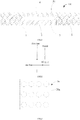
FIG. 1 is a schematic cross-sectional view illustrating a transparent OLED substrate according to an example of the present application. -
FIG. 2 is a schematic diagram illustrating a drive circuit of a first electrode of a transparent OLED substrate according to an example of the present application. -
FIG. 3 is a schematic top view illustrating a first electrode layer of a transparent OLED substrate according to an example of the present application. -
FIG. 4 is a schematic top view illustrating a first electrode layer of a transparent OLED substrate according to another example of the present application. -
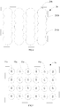
FIG. 5 is a schematic top view illustrating a light emitting structure layer of a transparent OLED substrate according to an example of the present application. -
FIG. 6 is a schematic top view illustrating a light emitting structure layer of a transparent OLED substrate according to another example of the present application. -
FIG. 7 is a schematic top view illustrating a first electrode layer and a light emitting structure layer of a transparent OLED substrate according an example of to the present application. -
FIG. 8 is a schematic top view illustrating a first electrode layer and a light emitting structure layer of a transparent OLED substrate according to another example of the present application. -
FIG. 9 is a schematic cross-sectional view illustrating a first OLED substrate of an array substrate according to an example of the present application. -
FIG. 10 is a schematic structural diagram illustrating a display screen according to an example of the present application. -
FIG. 11 is a schematic structural diagram illustrating a display device according to an example of the present application. - Examples will be described in detail herein, with the illustrations thereof represented in the drawings. When the following descriptions involve the drawings, like numerals in different drawings refer to same or similar elements unless otherwise indicated. The embodiments described in the following examples do not represent all embodiments consistent with the present disclosure. Rather, they are merely examples of apparatuses consistent with some aspects of the present disclosure as detailed in the appended claims.
- The above-mentioned display terminal or electronic device cannot display images in a camera area. Moreover, a light transmittance of the display terminal is not high. In this case, in order to improve the light transmittance, a display area in a substrate corresponding to a photosensitive element is set as a transparent display area with a lower pixel density according to the present application and a pixel density of a normal display area other than the transparent display area remains unchanged. Further, the pixel density may be lowered by reducing the number of light emitting structures in the transparent display area, and the number of light emitting structures in the normal display area remains unchanged. However, in contrast, if the same precise mask is used to fabricate the light emitting structures in the normal display area and the transparent display area, openings in a first area in the mask corresponding to the normal display area are denser, while openings in a second area in the mask corresponding to the transparent display area are sparse, which easily leads to uneven stresses at boundaries of the first area and the second area in the mask, and further to wrinkles formed at the boundaries of the first area and the second area in the mask, thereby causing a risk of color mixing between the normal display area and the transparent display area of the substrate.
- In order to solve the above technical problems, as shown in
FIGS. 1 ,9 and11 , in an example, an array substrate is provided, comprising abase substrate 1, afirst OLED substrate 200, and asecond OLED substrate 100. Thefirst OLED substrate 200 is a non-transparent OLED substrate, and at least partially surrounds thesecond OLED substrate 100. Thesecond OLED substrate 100 includes afirst electrode layer 2 located on the base substrate, a lightemitting structure layer 3 located on thefirst electrode layer 2, and asecond electrode layer 4 located on the lightemitting structure layer 3. Thefirst electrode layer 2 includes a plurality of first electrodes. The lightemitting structure layer 3 includes a plurality of light emitting structures. The number of the first electrodes is less than the number of the light emitting structures. Each of the first electrodes corresponds to one of the light emitting structures. - The number of the first electrodes is less than the number of the light emitting structures, and each of the first electrodes corresponds to one of the light emitting structures. That is to say, first electrodes below a part of the light emitting structures are omitted, and thus pixel circuits below the part of the light emitting structures are omitted, thereby causing the part of the light emitting structures not to emit light. This reduces a pixel density of the transparent OLED substrate, i.e., a pixel density of the
second OLED substrate 100 to increase a light transmittance thereof, so that a structure of the light emitting structure layer may remain unchanged (relative to other non-transparent display areas). In this way, openings in different areas of a mask are uniformly distributed, and stresses at boundaries of the different areas are also uniform. Under the premise that the transparent OLED substrate has a sufficient light transmittance, there will be no risk of color mixing at boundaries of the transparent OLED substrate and other display areas (the first OLED substrate as described above) due to wrinkles formed in a mask. -
FIG. 1 is a schematic structural diagram illustrating a transparent OLED substrate 100 (i.e., a second OLED substrate) in an example. Referring toFIG. 1 , thetransparent OLED substrate 100 includes afirst electrode layer 2 located on abase substrate 1, a lightemitting structure layer 3 located on thefirst electrode layer 2, and asecond electrode layer 4 located on the lightemitting structure layer 3. Thetransparent OLED substrate 100 further includes apixel definition layer 5. Thefirst electrode layer 2 is formed on thebase substrate 1. Thepixel definition layer 5 is formed on thefirst electrode layer 2. Thepixel definition layer 5 has a plurality ofpixel openings 51 in which the light emittingstructure layer 3 located on thefirst electrode layer 2 is formed, and thesecond electrode layer 4 is formed on the light emittingstructure layer 3. Thefirst electrode layer 2 may be an anode layer. Correspondingly, thesecond electrode layer 4 is a cathode layer. In other examples, the first electrode layer may be a cathode layer, and the second electrode layer is correspondingly an anode layer. - In an example, the
base substrate 1 may be a rigid substrate such as a glass substrate, a quartz substrate, a plastic substrate or other transparent substrates. In another example, thebase substrate 1 may be a flexible substrate such as a flexible PI substrate. - In an example, in order to improve the light transmittance of the transparent OLED substrate, materials of conductive wires of the transparent OLED substrate such as the
first electrode layer 2 and thesecond electrode layer 4 may include transparent materials. Light transmittances of the first electrode layer and the second electrode layer are greater than 40%, further greater than 60%, and still further not less than 80%. For example, materials of thefirst electrode layer 2 and thesecond electrode layer 4 may include a transparent conductive metal oxide or a mixture of magnesium and silver. For example, the materials of thefirst electrode layer 2 and thesecond electrode layer 4 may include at least one of indium tin oxide (ITO), indium zinc oxide (IZO), silver-doped ITO, or silver-doped IZO. - In an example, the
second electrode layer 4 is a planar electrode. Optionally, thesecond electrode layer 4 has a single layer structure or a stack structure. When thesecond electrode layer 4 has the single layer structure, thesecond electrode layer 4 is a single metal layer or a single metal mixture layer or a single transparent metal oxide layer. When thesecond electrode layer 4 has the stack structure, thesecond electrode layer 4 is a stack in which a transparent metal oxide layer and a metal layer are laminated, or a stack in which a transparent metal oxide layer and a metal mixture layer are laminated. - In an example, when materials of the
second electrode layer 4 are doped with a metal and a thickness of thesecond electrode layer 4 is greater than or equal to 100 angstroms and less than or equal to 500 angstroms, thesecond electrode layer 4 is an integral and continuous planar electrode, and has a transparency greater than 40%; when the materials of thesecond electrode layer 4 are doped with a metal and the thickness of thesecond electrode layer 4 is greater than or equal to 100 angstroms and less than or equal to 200 angstroms, thesecond electrode layer 4 is an integral and continuous planar electrode and has a transparency greater than 40%; when the materials of thesecond electrode layer 4 are doped with a metal and the thickness of thesecond electrode layer 4 is greater than or equal to 50 angstroms and less than or equal to 200 angstroms, thesecond electrode layer 4 is an integral and continuous planar electrode and has a transparency greater than 50%; when the materials of thesecond electrode layer 4 are doped with a metal and the thickness of thesecond electrode layer 4 is greater than or equal to 50 angstroms and less than or equal to 200 angstroms, thesecond electrode layer 4 is an integral and continuous planar electrode and has a transparency greater than 60%. When thesecond electrode layer 4 has a single layer structure, materials of the single metal layer include Al or Ag, materials of the single metal mixture layer include MgAg or a Al-doped metal mixture, and materials of the transparent metal oxide layer is ITO or IZO. - The
first electrode layer 2 includes a plurality of first electrodes 20, as shown inFIGS. 3 to 8 . A drive circuit of a first electrode 20 is a 2T1C drive circuit, including 2 thin film transistors (TFTs) and 1 capacitor, and a data line provides a data voltage signal for the first electrode. Compared with a 7T1C (7 TFTs and 1 capacitor) drive circuit of an OLED substrate, the 2T1C drive circuit is simpler, reducing the complexity of the drive circuit and facilitating to further improve the light transmittance of the transparent OLED substrate. - In another example, the drive circuit of the first electrode includes 1 TFT. With reference to
FIG. 2 , the transparent OLED substrate includes a scan line Scan and a data line Data. The data line Data is electrically connected to a source electrode of the TFT. The first electrode (indicated by OLED inFIG. 2 ) is electrically connected to a drain electrode of the TFT. The scan line Scan is electrically connected to a gate electrode of the TFT. The scan line Scan is used to control the drive circuit to turn on and off. The data line Data, when the drive circuit is turned on, provides a drive current signal for the first electrode to control the light emitting structure layer to emit light. The number of switch devices in the drive circuit is reduced to two or one, which greatly reduces load currents of the scan line and the data line, on the basis of simplifying the complexity of a panel structure and reducing diffraction caused by a gap of the panel structure, to reduce requirements for resistances of materials of conductive wires such as an anode, a cathode, scan lines and data lines. In this way, the conductive wires such as the anode, the cathode, scan lines, data lines and the like may be made of a transparent material so as to improve the light transmittance of the display panel while ensuring the performance of the panel. In another example, the data line Data is electrically connected to the drain electrode of the TFT, the first electrode (indicated by OLED inFIG. 2 ) is electrically connected to the source electrode of the TFT, and the scan line Scan is electrically connected to the gate electrode of the TFT. - With reference to
FIGS. 3 and4 , afirst electrode 20a of afirst electrode layer 2a is circular or gourd-shaped, but thefirst electrode 20a may also have other shapes such as a square, an oval, a dumbbell shape or a wave shape. Thefirst electrode 20a shown inFIG. 3 is circular. In some examples, the square may include a right-angled square or a rounded square. In an example, thefirst electrodes 20a in the same row or column correspond to light emitting structures of a same color, and thefirst electrodes 20a in the same row or column receive the same data signal. One data signal may drive the entire row or column of thefirst electrodes 20a, thereby simplifying the structure of the drive circuit. Thefirst electrodes 20a in the same row or column may be connected via connecting lines (not shown). The connecting lines may be routed through other film layers or non-display areas. - A
first electrode 20b of thefirst electrode layer 2b shown inFIG. 4 is gourd-shaped, and extends along a first direction. The first direction is a row or column direction of the transparent OLED substrate (the row direction is a scan line direction, and the column direction is a data line direction). InFIG. 4 , the first direction is a column direction of the array substrate. In this example, thefirst electrode 20b is formed by sequentially connecting a plurality of first sub-electrodes 201b in the same column, and each of the first sub-electrodes 201b corresponds to one light emitting structure. Thefirst electrode 20b is connected to the same data line through one drive circuit, thereby reducing the number of the drive circuit and simplifying the structure of the drive circuit. In this example, thesecond electrode layer 4 is a planar electrode. - Referring to
FIG. 5 , a light emittingstructure layer 3a includes a plurality of light emittingstructures 30a. Thelight emitting structures 30a shown inFIG. 5 are circular. The light emittingstructure layer 3a includes light emitting structures of n colors. If n is equal to 3, the light emittingstructure layer 3a includes a red firstlight emitting structure 31a, a green secondlight emitting structure 32a, and a blue thirdlight emitting structure 33a.Light emitting structures 30b shown inFIG. 6 are square. In other examples, the light emitting structure has an oval shape, a dumbbell shape or the like. In some examples, the light emitting structures in the same row or column have the same color, as shown inFIGS. 5 and6 . -
FIG. 7 is a schematic top view illustrating a first electrode layer and a light emitting structure layer of a transparent OLED substrate according to an example of the present application. The first electrode layer includes a plurality offirst electrodes 20c. Thefirst electrodes 20c have a rounded square shape. The light emitting structure layer includes a plurality of light emitting structures. The light emitting structures also have a rounded square shape. The number of thefirst electrodes 20c is less than the number of thelight emitting structures 30c. Each of thefirst electrodes 20c corresponds to onelight emitting structure 30c. Due to that the number of thelight emitting structures 30c is larger in comparison, thefirst electrodes 20c are not disposed below a part of the light emitting structures and the area corresponding to the part of the light emitting structures has a higher light transmittance. When the transparent OLED substrate is working, the part of the light emitting structures does not emit light. - With continued reference to
FIG. 7 , the light emitting structure layer includes a plurality of pixel units C arranged in an array. Each of the pixel units C includes light emitting structures of three colors, i.e., green, red and blue, in which at least two light emitting structures of the same color are included. In the at least two light emitting structures of the same color, thefirst electrodes 20c are disposed below a part of the light emitting structures while thefirst electrodes 20c are not disposed below the other part of the light emitting structures, which improves the light transmittance of the transparent OLED substrate without affecting the normal display effect of the transparent OLED substrate. As shown inFIG. 7 , each of the pixel units C includes a firstlight emitting structure 31c, a secondlight emitting structure 32c, a thirdlight emitting structure 33c and a fourthlight emitting structure 34c corresponding to four colors, green, green, red and blue in sequence (R, G and B represent only colors of the light emitting structures, and letters in the drawing are marked only on overlapping areas of the first electrodes and the light emitting structures). That is, each of the pixel units C includes light emitting structures of three colors. Thefirst electrode 20c is not disposed below the green secondlight emitting structure 32c. That is, one of the two green light emitting structures in one pixel unit C emits light, and the other does not emit light, which improves the light transmittance of the transparent OLED substrate without affecting the normal display effect of the transparent OLED substrate. In other examples, alternatively, thefirst electrode 20c is not disposed below a light emitting structure of another color. For example, thefirst electrode 20c is not disposed below a blue second light emitting structure, or thefirst electrode 20c is not disposed below a red second light emitting structure. - In
FIG. 7 , in the column direction as the first direction, the firstlight emitting structures 31c and the secondlight emitting structures 32c which actually do not emit light, are arranged alternately to ensure that the transparent OLED substrate displays uniformly in the first direction. For example, the firstlight emitting structures 31c and the secondlight emitting structures 32c which actually do not emit light in the same column are arranged at intervals. In the entire light emitting structure layer, since the pixel units are arranged in an array, the secondlight emitting structures 32c which actually do not emit light in the plurality of pixel units C are correspondingly arranged in an array, facilitating to improve the overall display uniformity of the transparent OLED substrate. - Referring to
FIG. 8 , in another example, the light emitting structure layer includes a plurality of first pixel units D and second pixel units E arranged in an array. Each of the first pixel units D includes light emitting structures of n colors. In this example, n is equal to 3, the three colors are red, green and blue. Each of the first pixel units D includes a redlight emitting structure 31d, a greenlight emitting structure 32d, and a bluelight emitting structure 33d. Each of the redlight emitting structure 31d, the greenlight emitting structure 32d and the bluelight emitting structure 33d corresponds to onefirst electrode 20d. Each of second pixel units E includes light emitting structures of n colors. In this example, n is equal to 3, and the light emitting structures of n colors are, for example, red, green and blue light emitting structures. Each of the second pixel units includes a redlight emitting structure 31e, a greenlight emitting structure 32e, and a bluelight emitting structure 33e. Thefirst electrodes 20d are not disposed below the redlight emitting structure 31e, the greenlight emitting structure 32e, and the bluelight emitting structure 33e. That is, after the transparent OLED substrate is powered on, the first pixel units D emit light, and the second pixel units E do not emit light, which improve the light transmittance of the transparent OLED substrate without affecting the display effect of the transparent OLED substrate. - In
FIG. 8 , in the column direction as the first direction, the first pixel units D and the second pixel units E which actually do not emit light are alternately arranged to ensure that the transparent OLED substrate displays uniformly in the first direction. In the entire light emitting structure layer, the second pixel units E are arranged in an array, facilitating to improve the overall display uniformity of the transparent OLED substrate. - The array substrate provided by the present application includes the
first OLED substrate 200 as shown inFIG. 9 , and thesecond OLED substrate 100 as shown inFIG. 1 . Thefirst OLED substrate 200 at least partially surrounds thesecond OLED substrate 100, as described inFIG. 11 . The area corresponding to thefirst OLED substrate 200 on the array substrate may be rectangular or circular. The area corresponding to thesecond OLED substrate 100 on the array substrate may be circular, rectangular, drop-shaped, bang-shaped, etc. The second OLED substrate is thetransparent OLED substrate 100 described in any of the previous examples. - With reference to
FIG. 9 , thefirst OLED substrate 200 includes athird electrode layer 7 formed on thebase substrate 1, a light emittingmaterial layer 8 formed on thethird electrode layer 7, and afourth electrode layer 9 formed on the light emittingmaterial layer 8. Thethird electrode layer 7 includes a plurality of third electrodes. The light emittingmaterial layer 8 includes a plurality of light emitting materials. The third electrodes correspond to the light emitting materials one to one. In an example, the light emittingmaterial layer 8 of the first OLED substrate and the light emittingstructure layer 3 of the second OLED substrate are formed using the same mask during the same process. The adjacent light emitting structures of the light emittingstructure layer 3 and the adjacent light emitting materials of the light emittingmaterial layer 8 may have the same sizes and the equal spacing. The area in the mask corresponding to the first OLED substrate and the area in the mask corresponding to the second OLED substrate may be provided with mask openings of the same size. Since opening sizes and opening spacing are equal, stresses at the boundary of the two areas are uniform, avoiding wrinkles formed at the boundary of the first OLED substrate and the second OLED substrate. At the same time, the first electrodes are not disposed below a part of the light emitting structures included in the light emittingstructure layer 3 of the second OLED substrate, ensuring that the second OLED substrate has a sufficiently large light transmittance under the premise of normal display. - The present application further provides a display screen, as shown in
FIG. 11 , comprising the array substrate as described above, and anencapsulating layer 201 for encapsulating the array substrate. An area corresponding to thefirst OLED substrate 200 is a non-transparent display area. An area corresponding to thesecond OLED substrate 100 is a transparent display area. Optionally, the transparent display area corresponds to a PMOLED screen, and the non-transparent display area corresponds to an AMOLED screen. photosensitive elements such as a camera and a sensor may be disposed below the PMOLED screen. The photosensitive elements may collect external lights through the transparent PMOLED screen. The display screen ensures the performance of the photosensitive elements while achieving a display function. - With reference to
FIG. 11 , the present application further provides a display device. The display device includes adevice body 300, and a display screen covering the device body. The display device may be a mobile phone, a tablet computer, a notebook computer or other devices. Taking the mobile phone as an example, the device body may include elements such as a house, a circuit board, a battery and a processor. Thedevice body 300 also has a component area. The component area is located below thesecond OLED substrate 100, and aphotosensitive element 400 that collects lights through thesecond OLED substrate 100 is disposed in the component area. Thephotosensitive element 400 may be a camera, an infrared sensor or other optical sensors. Due to the high light transmittance of thesecond OLED substrate 100, it is ensured that the photosensitive element collects sufficient light. - The above descriptions are only preferred examples of the present application, and are not intended to limit the application. Any modification, equivalent replacement, improvement, etc. made within the spirit and principle of this application shall be contained within the protection scope of the application.
Claims (18)
- An array substrate, comprisinga base substrate;a non-transparent first OLED substrate at least partially surrounding a transparent second OLED substrate; andthe transparent second OLED substrate comprisinga first electrode layer located on the base substrate;a light emitting structure layer located on the first electrode layer; anda second electrode layer located on the light emitting structure layer,wherein the first electrode layer comprises a plurality of first electrodes, the light emitting structure layer comprises a plurality of light emitting structures, a number of the first electrodes is less than a number of the light emitting structures, and each of the first electrodes corresponds to one of the light emitting structures.
- The array substrate according to claim 1, wherein the light emitting structure layer comprises first light emitting structures and second light emitting structures of a same color, the first light emitting structures correspond to the first electrodes one to one, and the first electrodes are not disposed below the second light emitting structures.
- The array substrate according to claim 2, wherein the light emitting structure layer comprises a plurality of pixel units, each of which comprises the first light emitting structure and the second light emitting structure;
the first light emitting structures and the second light emitting structures are alternately arranged in a first direction which is a row direction or a column direction of the array substrate. - The array substrate according to claim 1, wherein the light emitting structure layer comprises a plurality of first pixel units and a plurality of second pixel units, each of the first pixel units and each of the second pixel units comprise light emitting structures of n colors, each of the light emitting structures in the first pixel units corresponds to one of the first electrodes, and the first electrodes are not disposed below each of the light emitting structures in the second pixel units.
- The array substrate according to claim 4, wherein the first pixel units and the second pixel units are alternately arranged in a first direction which is a row direction or a column direction of the array substrate.
- The array substrate according to claim 2, wherein the second light emitting structures are arranged in an array.
- The array substrate according to claim 4, wherein the second pixel units are arranged in an array.
- The array substrate according to claim 1, wherein a drive circuit of the first electrodes is a drive circuit comprising two thin film transistors and one storage capacitor; or
the drive circuit of the first electrodes comprises one thin film transistor, the second OLED substrate comprises a data line which is electrically connected to a source electrode or a drain electrode of the thin film transistor, the first electrodes are electrically connected to the drain electrode or the source electrode of the thin film transistor, and the data line provides a drive current for the first electrodes to control the light emitting structure layer to emit light when the drive circuit is turned on. - The array substrate according to claim 1, wherein the light emitting structures corresponding to the first electrodes in the same row or column have a same color, and the first electrodes in the same row or column receive a same data signal.
- The array substrate according to claim 1, wherein the first electrodes are circular, square, oval, dumbbell-shaped, gourd-shaped or wave-shaped, and the light emitting structures are square, circular, oval or dumbbell-shaped.
- The array substrate according to claim 1, wherein the first OLED substrate comprises a third electrode layer, a light emitting material layer formed on the third electrode layer, and a fourth electrode layer formed on the light emitting material layer,the third electrode layer comprises a plurality of third electrodes, the light emitting material layer comprises a plurality of light emitting materials, andthe third electrodes correspond to the light emitting materials one to one.
- The array substrate according to claim 11, wherein the light emitting material layer of the first OLED substrate and the light emitting structure layer of the second OLED substrate are formed using a same mask during a same process.
- The array substrate according to claim 11, wherein both an area in the mask corresponding to the first OLED substrate and an area in the mask corresponding to the second OLED substrate are provided with mask openings of a same size.
- The array substrate according to claim 12, wherein adjacent light emitting structures in the light emitting structure layer and adjacent light emitting materials in the light emitting material layer have a same size and an equal spacing.
- The array substrate according to claim 1, wherein the first electrode layer and the second electrode layer have a light transmittance greater than 40%, and materials of the first electrode layer and the second electrode layer comprise a transparent conductive metal oxide or a mixture of magnesium and silver.
- The array substrate according to claim 1, wherein the second electrode layer is a planar electrode, and the second electrode layer has a single layer structure or a stack structure;when the second electrode layer has the single layer structure, the second electrode layer is a single metal layer or a single metal mixture layer or a single transparent metal oxide layer,when the second electrode layer has the stack structure, the second electrode layer is a stack in which a transparent metal oxide layer and a metal layer are laminated, or a stack in which a transparent metal oxide layer and a metal mixture layer are laminated;when a material of the second electrode layer is doped with a metal and a thickness of the second electrode layer is greater than or equal to 100 angstroms and less than or equal to 500 angstroms, the second electrode layer is an integral and continuous planar electrode and has a transparency greater than 40%;when the material of the second electrode layer is doped with the metal and the thickness of the second electrode layer is greater than or equal to 100 angstroms and less than or equal to 200 angstroms, the second electrode layer is an integral and continuous planar electrode and has a transparency greater than 40%;when the material of the second electrode layer is doped with the metal and the thickness of the second electrode layer is greater than or equal to 50 angstroms and less than or equal to 200 angstroms, the second electrode layer is an integral and continuous planar electrode and has a transparency greater than 50%;when the material of the second electrode layer is doped with the metal and the thickness of the second electrode layer is greater than or equal to 50 angstroms and less than or equal to 200 angstroms, the second electrode layer is an integral and continuous planar electrode and has a transparency greater than 60%;when the second electrode layer has the single layer structure, a material of the single metal layer comprises Al, Ag, a material of the single metal mixture layer comprises Mg, Ag or a metal mixture doped with Al, and the transparent metal oxide is indium tin oxide or indium zinc oxide.
- A display screen, comprisingan array substrate according to claim 1; andan encapsulating layer for encapsulating the array substrate.
- A display device, comprisinga device body having a component area; anda display screen according to claim 17 covering the device body,wherein the component area is located below a second OLED substrate, and a photosensitive element that collects lights through the second OLED substrate is disposed in the component area.
Applications Claiming Priority (2)
| Application Number | Priority Date | Filing Date | Title |
|---|---|---|---|
| CN201910097327.8A CN110767833B (en) | 2019-01-31 | 2019-01-31 | Transparent OLED substrate, array substrate, display screen and display device |
| PCT/CN2019/095041 WO2020155560A1 (en) | 2019-01-31 | 2019-07-08 | Array substrate, display screen and display device |
Publications (2)
| Publication Number | Publication Date |
|---|---|
| EP3920253A1 true EP3920253A1 (en) | 2021-12-08 |
| EP3920253A4 EP3920253A4 (en) | 2022-06-15 |
Family
ID=69328570
Family Applications (1)
| Application Number | Title | Priority Date | Filing Date |
|---|---|---|---|
| EP19913316.6A Pending EP3920253A4 (en) | 2019-01-31 | 2019-07-08 | MATRIX SUBSTRATE, DISPLAY SCREEN AND DISPLAY DEVICE |
Country Status (6)
| Country | Link |
|---|---|
| US (1) | US11417715B2 (en) |
| EP (1) | EP3920253A4 (en) |
| JP (1) | JP2022505249A (en) |
| KR (1) | KR20210052554A (en) |
| CN (1) | CN110767833B (en) |
| WO (1) | WO2020155560A1 (en) |
Families Citing this family (4)
| Publication number | Priority date | Publication date | Assignee | Title |
|---|---|---|---|---|
| CN113838889B (en) * | 2020-06-23 | 2024-08-20 | 京东方科技集团股份有限公司 | Display substrate, display panel, electronic device and display method |
| WO2024214132A1 (en) * | 2023-04-10 | 2024-10-17 | シャープディスプレイテクノロジー株式会社 | Display device |
| CN117975882A (en) * | 2023-12-29 | 2024-05-03 | 湖北长江新型显示产业创新中心有限公司 | Display panel and pixel repair method thereof, and display device |
| CN118102767B (en) * | 2024-04-23 | 2024-08-16 | 浙江大学 | LED semiconductor device for optical communication and preparation method thereof |
Family Cites Families (19)
| Publication number | Priority date | Publication date | Assignee | Title |
|---|---|---|---|---|
| JP2004226673A (en) * | 2003-01-23 | 2004-08-12 | Toyota Industries Corp | Organic electroluminescent device |
| KR101097454B1 (en) * | 2009-02-16 | 2011-12-23 | 네오뷰코오롱 주식회사 | Pixel circuit for organic light emitting diode(oled) panel, display device having the same, and method of driving oled panel using the same |
| CN102351435B (en) * | 2010-06-02 | 2015-07-08 | 松下电器产业株式会社 | Coating method and manufacturing method of organic electroluminescent display |
| KR102071009B1 (en) * | 2013-10-10 | 2020-01-30 | 삼성디스플레이 주식회사 | Organic light emitting diode display and repairing method thereof |
| KR102211965B1 (en) * | 2013-10-18 | 2021-02-05 | 삼성디스플레이 주식회사 | Organic light emitting display device |
| US10644077B1 (en) * | 2015-10-28 | 2020-05-05 | Apple Inc. | Display with array of light-transmitting windows |
| CN106921767A (en) * | 2017-03-07 | 2017-07-04 | 捷开通讯(深圳)有限公司 | A kind of mobile terminal of screen accounting high |
| CN109285860B (en) * | 2017-07-21 | 2025-02-07 | 京东方科技集团股份有限公司 | Electroluminescent display panel, display device and image display method thereof |
| CN207338380U (en) * | 2017-07-21 | 2018-05-08 | 京东方科技集团股份有限公司 | A kind of electroluminescence display panel and display device |
| CN107622749B (en) * | 2017-09-08 | 2019-10-01 | 上海天马有机发光显示技术有限公司 | A kind of display panel, electroluminescence display panel and display device |
| CN108364967B (en) | 2017-09-30 | 2021-07-27 | 昆山国显光电有限公司 | Displays and Display Devices |
| CN108257514A (en) * | 2017-09-30 | 2018-07-06 | 昆山国显光电有限公司 | Display screen, display panel drive method and its display device |
| CN107819018B (en) * | 2017-10-31 | 2020-11-10 | 武汉天马微电子有限公司 | Electroluminescent display panel and display device |
| CN107994054B (en) * | 2017-11-07 | 2020-05-29 | 上海天马有机发光显示技术有限公司 | An organic electroluminescence display panel, its manufacturing method and display device |
| CN107731883A (en) * | 2017-11-17 | 2018-02-23 | 深圳市华星光电半导体显示技术有限公司 | OLED display and preparation method thereof |
| CN108598115A (en) | 2018-04-24 | 2018-09-28 | 武汉华星光电技术有限公司 | Oled display panel |
| CN108428729B (en) * | 2018-05-14 | 2019-12-24 | 云谷(固安)科技有限公司 | Display panel and manufacturing method thereof |
| CN108983872B (en) * | 2018-06-04 | 2021-07-13 | Oppo广东移动通信有限公司 | Electronic device and control method thereof |
| CN109001934A (en) * | 2018-09-21 | 2018-12-14 | 北京小米移动软件有限公司 | Electronic equipment |
-
2019
- 2019-01-31 CN CN201910097327.8A patent/CN110767833B/en active Active
- 2019-07-08 JP JP2021521211A patent/JP2022505249A/en active Pending
- 2019-07-08 EP EP19913316.6A patent/EP3920253A4/en active Pending
- 2019-07-08 KR KR1020217011468A patent/KR20210052554A/en not_active Ceased
- 2019-07-08 WO PCT/CN2019/095041 patent/WO2020155560A1/en not_active Ceased
-
2021
- 2021-01-07 US US17/143,416 patent/US11417715B2/en active Active
Also Published As
| Publication number | Publication date |
|---|---|
| CN110767833A (en) | 2020-02-07 |
| JP2022505249A (en) | 2022-01-14 |
| KR20210052554A (en) | 2021-05-10 |
| EP3920253A4 (en) | 2022-06-15 |
| CN110767833B (en) | 2021-02-09 |
| US11417715B2 (en) | 2022-08-16 |
| US20210134909A1 (en) | 2021-05-06 |
| WO2020155560A1 (en) | 2020-08-06 |
Similar Documents
| Publication | Publication Date | Title |
|---|---|---|
| US12089443B2 (en) | Display panel and display device | |
| US12075673B2 (en) | Display panel comprising a data line including sub-data lines and display device having the same | |
| US20210141304A1 (en) | Mask strips, array substrates and display screens | |
| US12484375B2 (en) | Display panel and display apparatus | |
| EP3951882B1 (en) | Display panel and display apparatus | |
| US20210013277A1 (en) | Array substrate, display panel and display apparatus | |
| US11417715B2 (en) | Array substrate, display screen and display device | |
| US11387281B2 (en) | Array substrate, display panel and display device, enabling full screen display with transparent and non-transparent display areas | |
| CN110767681B (en) | Display screen and display terminal | |
| TW202423271A (en) | Display device | |
| CN114141851A (en) | Display panel, display screen and electronic equipment | |
| CN110265472A (en) | Display panel and display device | |
| CN111430436A (en) | Display panel and display device | |
| WO2020087799A1 (en) | Display screen and display terminal | |
| CN110061044A (en) | Organic light emitting display panel and display device | |
| CN108364993B (en) | Display panel manufacturing method, display panel and display device | |
| EP4488987A1 (en) | Display panel and display apparatus | |
| CN108682390A (en) | A kind of display device and its brightness detection method | |
| CN113299720A (en) | A display panel and display device | |
| CN110767166B (en) | Display screen and display terminal | |
| CN110767685B (en) | Display screen and display terminal | |
| CN110767686B (en) | Display screen and display terminal | |
| US12414419B2 (en) | Display substrate | |
| US20250374793A1 (en) | Touch display substrate and touch display apparatus | |
| US20240397780A1 (en) | Display substrate and display device |
Legal Events
| Date | Code | Title | Description |
|---|---|---|---|
| STAA | Information on the status of an ep patent application or granted ep patent |
Free format text: STATUS: THE INTERNATIONAL PUBLICATION HAS BEEN MADE |
|
| PUAI | Public reference made under article 153(3) epc to a published international application that has entered the european phase |
Free format text: ORIGINAL CODE: 0009012 |
|
| STAA | Information on the status of an ep patent application or granted ep patent |
Free format text: STATUS: REQUEST FOR EXAMINATION WAS MADE |
|
| 17P | Request for examination filed |
Effective date: 20210419 |
|
| AK | Designated contracting states |
Kind code of ref document: A1 Designated state(s): AL AT BE BG CH CY CZ DE DK EE ES FI FR GB GR HR HU IE IS IT LI LT LU LV MC MK MT NL NO PL PT RO RS SE SI SK SM TR |
|
| DAV | Request for validation of the european patent (deleted) | ||
| DAX | Request for extension of the european patent (deleted) | ||
| REG | Reference to a national code |
Ref country code: DE Ref legal event code: R079 Free format text: PREVIOUS MAIN CLASS: H01L0051520000 Ipc: H01L0027320000 |
|
| A4 | Supplementary search report drawn up and despatched |
Effective date: 20220512 |
|
| RIC1 | Information provided on ipc code assigned before grant |
Ipc: H01L 51/52 20060101ALI20220506BHEP Ipc: H01L 27/32 20060101AFI20220506BHEP |
|
| STAA | Information on the status of an ep patent application or granted ep patent |
Free format text: STATUS: EXAMINATION IS IN PROGRESS |
|
| 17Q | First examination report despatched |
Effective date: 20250714 |