EP3917035A1 - Optical modulating device - Google Patents
Optical modulating device Download PDFInfo
- Publication number
- EP3917035A1 EP3917035A1 EP21174816.5A EP21174816A EP3917035A1 EP 3917035 A1 EP3917035 A1 EP 3917035A1 EP 21174816 A EP21174816 A EP 21174816A EP 3917035 A1 EP3917035 A1 EP 3917035A1
- Authority
- EP
- European Patent Office
- Prior art keywords
- optical
- optical signal
- modulating
- signal
- split
- Prior art date
- Legal status (The legal status is an assumption and is not a legal conclusion. Google has not performed a legal analysis and makes no representation as to the accuracy of the status listed.)
- Withdrawn
Links
Images


Classifications
-
- G—PHYSICS
- G02—OPTICS
- G02F—OPTICAL DEVICES OR ARRANGEMENTS FOR THE CONTROL OF LIGHT BY MODIFICATION OF THE OPTICAL PROPERTIES OF THE MEDIA OF THE ELEMENTS INVOLVED THEREIN; NON-LINEAR OPTICS; FREQUENCY-CHANGING OF LIGHT; OPTICAL LOGIC ELEMENTS; OPTICAL ANALOGUE/DIGITAL CONVERTERS
- G02F1/00—Devices or arrangements for the control of the intensity, colour, phase, polarisation or direction of light arriving from an independent light source, e.g. switching, gating or modulating; Non-linear optics
- G02F1/01—Devices or arrangements for the control of the intensity, colour, phase, polarisation or direction of light arriving from an independent light source, e.g. switching, gating or modulating; Non-linear optics for the control of the intensity, phase, polarisation or colour
- G02F1/21—Devices or arrangements for the control of the intensity, colour, phase, polarisation or direction of light arriving from an independent light source, e.g. switching, gating or modulating; Non-linear optics for the control of the intensity, phase, polarisation or colour by interference
- G02F1/225—Devices or arrangements for the control of the intensity, colour, phase, polarisation or direction of light arriving from an independent light source, e.g. switching, gating or modulating; Non-linear optics for the control of the intensity, phase, polarisation or colour by interference in an optical waveguide structure
-
- H—ELECTRICITY
- H04—ELECTRIC COMMUNICATION TECHNIQUE
- H04B—TRANSMISSION
- H04B10/00—Transmission systems employing electromagnetic waves other than radio-waves, e.g. infrared, visible or ultraviolet light, or employing corpuscular radiation, e.g. quantum communication
- H04B10/25—Arrangements specific to fibre transmission
- H04B10/2507—Arrangements specific to fibre transmission for the reduction or elimination of distortion or dispersion
- H04B10/2513—Arrangements specific to fibre transmission for the reduction or elimination of distortion or dispersion due to chromatic dispersion
- H04B10/25137—Arrangements specific to fibre transmission for the reduction or elimination of distortion or dispersion due to chromatic dispersion using pulse shaping at the transmitter, e.g. pre-chirping or dispersion supported transmission [DST]
-
- H—ELECTRICITY
- H04—ELECTRIC COMMUNICATION TECHNIQUE
- H04B—TRANSMISSION
- H04B10/00—Transmission systems employing electromagnetic waves other than radio-waves, e.g. infrared, visible or ultraviolet light, or employing corpuscular radiation, e.g. quantum communication
- H04B10/50—Transmitters
- H04B10/516—Details of coding or modulation
- H04B10/548—Phase or frequency modulation
-
- G—PHYSICS
- G02—OPTICS
- G02F—OPTICAL DEVICES OR ARRANGEMENTS FOR THE CONTROL OF LIGHT BY MODIFICATION OF THE OPTICAL PROPERTIES OF THE MEDIA OF THE ELEMENTS INVOLVED THEREIN; NON-LINEAR OPTICS; FREQUENCY-CHANGING OF LIGHT; OPTICAL LOGIC ELEMENTS; OPTICAL ANALOGUE/DIGITAL CONVERTERS
- G02F1/00—Devices or arrangements for the control of the intensity, colour, phase, polarisation or direction of light arriving from an independent light source, e.g. switching, gating or modulating; Non-linear optics
- G02F1/01—Devices or arrangements for the control of the intensity, colour, phase, polarisation or direction of light arriving from an independent light source, e.g. switching, gating or modulating; Non-linear optics for the control of the intensity, phase, polarisation or colour
- G02F1/21—Devices or arrangements for the control of the intensity, colour, phase, polarisation or direction of light arriving from an independent light source, e.g. switching, gating or modulating; Non-linear optics for the control of the intensity, phase, polarisation or colour by interference
-
- G—PHYSICS
- G02—OPTICS
- G02B—OPTICAL ELEMENTS, SYSTEMS OR APPARATUS
- G02B6/00—Light guides; Structural details of arrangements comprising light guides and other optical elements, e.g. couplings
- G02B6/10—Light guides; Structural details of arrangements comprising light guides and other optical elements, e.g. couplings of the optical waveguide type
- G02B6/12—Light guides; Structural details of arrangements comprising light guides and other optical elements, e.g. couplings of the optical waveguide type of the integrated circuit kind
- G02B6/122—Basic optical elements, e.g. light-guiding paths
- G02B6/125—Bends, branchings or intersections
-
- G—PHYSICS
- G02—OPTICS
- G02B—OPTICAL ELEMENTS, SYSTEMS OR APPARATUS
- G02B6/00—Light guides; Structural details of arrangements comprising light guides and other optical elements, e.g. couplings
- G02B6/24—Coupling light guides
- G02B6/26—Optical coupling means
- G02B6/28—Optical coupling means having data bus means, i.e. plural waveguides interconnected and providing an inherently bidirectional system by mixing and splitting signals
- G02B6/293—Optical coupling means having data bus means, i.e. plural waveguides interconnected and providing an inherently bidirectional system by mixing and splitting signals with wavelength selective means
- G02B6/29346—Optical coupling means having data bus means, i.e. plural waveguides interconnected and providing an inherently bidirectional system by mixing and splitting signals with wavelength selective means operating by wave or beam interference
- G02B6/2935—Mach-Zehnder configuration, i.e. comprising separate splitting and combining means
-
- G—PHYSICS
- G02—OPTICS
- G02F—OPTICAL DEVICES OR ARRANGEMENTS FOR THE CONTROL OF LIGHT BY MODIFICATION OF THE OPTICAL PROPERTIES OF THE MEDIA OF THE ELEMENTS INVOLVED THEREIN; NON-LINEAR OPTICS; FREQUENCY-CHANGING OF LIGHT; OPTICAL LOGIC ELEMENTS; OPTICAL ANALOGUE/DIGITAL CONVERTERS
- G02F1/00—Devices or arrangements for the control of the intensity, colour, phase, polarisation or direction of light arriving from an independent light source, e.g. switching, gating or modulating; Non-linear optics
- G02F1/01—Devices or arrangements for the control of the intensity, colour, phase, polarisation or direction of light arriving from an independent light source, e.g. switching, gating or modulating; Non-linear optics for the control of the intensity, phase, polarisation or colour
- G02F1/21—Devices or arrangements for the control of the intensity, colour, phase, polarisation or direction of light arriving from an independent light source, e.g. switching, gating or modulating; Non-linear optics for the control of the intensity, phase, polarisation or colour by interference
- G02F1/212—Mach-Zehnder type
-
- H—ELECTRICITY
- H04—ELECTRIC COMMUNICATION TECHNIQUE
- H04B—TRANSMISSION
- H04B10/00—Transmission systems employing electromagnetic waves other than radio-waves, e.g. infrared, visible or ultraviolet light, or employing corpuscular radiation, e.g. quantum communication
- H04B10/50—Transmitters
- H04B10/501—Structural aspects
Definitions
- the present disclosure relates to a device, and particularly relates to an optical modulating device.
- optical fiber dispersion is a phenomenon that optical waves are dispersed into optical spectrum components with different wavelengths due to dependence of wave velocity on wavelength.
- an optical signal or pulse emitted by an optical modulating device is projected into, for example, an optical fiber channel, an envelope thereof propagates along the fiber channel at wave group velocities to an optical receiving device. Since this pulse contains a series of optical spectrum components, each optical spectrum component travels at a different wave group velocity, causing group velocity dispersion (GVD), intramodal dispersion or simple optical fiber dispersion.
- GGD group velocity dispersion
- This dispersion phenomenon also is often referred to as pulse broadening.
- the optical spectrum components continue to be dispersed in space and time, the pulse will become too wide, a front edge of a pulse overlaps a rear edge of a previous pulse, and inter symbol interference (ISI) will occur and the bit will be blurred, which causes that, when the optical receiving device receives the optical signal and demodulate based on the optical signal, the optical receiving device is unable to identify the difference between the "0" bit and the "1" bit and results in demodulation error.
- the dispersion of the optical fiber is directly ratio to a length of the optical fiber, that is, a transmission distance of the optical signal is limited by the dispersion of the optical fiber.
- SNR signal-to-noise ratio
- the signal-to-noise ratio and the dispersion of the optical fiber becomes one of the important factors affecting the signal quality of optical fiber communication. Therefore, how to avoid the signal-to-noise ratio being too low and the dispersion of the optical fiber seriously affecting the optical fiber communication system in order to promote the optical transmission distance is a subject to be improved by the relevant communication entities.
- an object of the present disclosure is to provide an optical modulating device which can overcome the deficiency of the existing technology.
- an optical modulating device of the present disclosure comprises an optical splitter, an optical phase modulator and an optical combiner.
- Thee optical splitter is used to receive an inputting optical signal and split the inputting optical signal by an optical splitting ratio to generate a first split optical signal and a second split optical signal.
- the optical phase modulator couples the optical splitter to receive the first split optical signal and the second split optical signal and phase modulate the first split optical signal and the second split optical signal to respectively generate a first modulating optical signal and a second modulating optical signal.
- the optical combiner couples the optical phase modulator to receive the first modulating optical signal and the second modulating optical signal and combine the first modulating optical signal and the second modulating optical signal by a combining ratio to generate an outputting optical signal having a chirp, the combining ratio being equal to the optical splitting ratio, a value of the combining ratio being a positive number, and the value being less than one or more than one.
- the effect of the present disclosure lies in that: by that the optical splitting ratio is equal to the optical combining ratio, it makes the outputting optical signal have a better signal-to-noise ratio, so that the optical receiving device has better demodulation accuracy when the optical receiving device receives the outputting optical signal and demodulates according to the outputting optical signal, and the outputting optical signal has the chirp, it may reduce effect of a dispersion caused by the optical fiber on transmission of the outputting optical signal, in turn promote transmission performance of the optical communication system.
- an embodiment of an optical modulating device 1 of the present disclosure is adapted to an optical communication system (not shown).
- the optical communication system includes an optical fiber (not shown) and an optical receiving device (not shown).
- the optical modulating device 1 is used to modulate an inputting optical signal Oin having a continuous wave, to generate and emit an outputting optical signal Oout having a chirp and transmit the outputting optical signal Oout to the optical receiving device via the optical fiber.
- the optical receiving device demodulates the outputting optical signal Oout received by the optical receiving device.
- the optical modulating device 1 of the present embodiment includes an optical splitter 11, an optical phase modulator 12 and an optical combiner 13.
- the optical modulating device 1 is a Mach-Zehnder modulator (MZM), the Mach-Zehnder modulator is made of one of a LiNbO 3 -based, a Silicon and an Inp.
- MZM Mach-Zehnder modulator
- the optical splitter 11 is used to receive the inputting optical signal Oin, and split the inputting optical signal Oin by an optical splitting ratio (that is, ⁇ 1:(1- ⁇ 1), 0 ⁇ 1 ⁇ 1), to generate a first split optical signal Os1 and a second split optical signal Os2.
- the optical splitter 11 is an optical directional coupler, and only receives the inputting optical signal Oin, but the present disclosure is not limited thereto.
- an inputting end 111 of the optical splitter 11 receives the inputting optical signal Oin, and another inputting end 112 receives another inputting optical signal.
- the optical splitter 11 may be a Y-branch waveguide or a multi-mode interferometer.
- the optical phase modulator 12 couples the optical splitter 11 to receive the first split optical signal Os1 and the second split optical signal Os2 and phase modulate the first split optical signal Os1 and the second split optical signal Os2, so as to respectively generate a first modulating optical signal Om1 and a second modulating optical signal Om2.
- the optical phase modulator 12 includes a first waveguide 121, a second waveguide 122, a first electrode 123, a second electrode 124 and a bias voltage electrode 125.
- the first waveguide 121 is coupled between the optical splitter 11 and the optical combiner 13, receives the first split optical signal Os1 from the optical splitter 11, and generates the first modulating optical signal Om1 based on the first split optical signal Os1.
- the second waveguide 122 is coupled between the optical splitter 11 and the optical combiner 13, receives the second split optical signal Os2 from the optical splitter 11, and generates the second modulating optical signal Om2 based on the second split optical signal Os2.
- the first electrode 123 is provided corresponding to the first waveguide 121, and is used to receive a first modulating voltage V1.
- the second electrode 124 is provided corresponding to the second waveguide 122, and is used to receive a second modulating voltage V2.
- the first electrode 123 and the second electrode 124 are provided on an upper surface of the first waveguide 121 and an upper surface of the second waveguide 122 respectively.
- the first electrode 123 and the second electrode 124 cause a refractive index of the first waveguide 121 itself and a refractive index of the second waveguide 122 itself to generate change respectively according to the first modulating voltage V1 and the second modulating voltage V2 (for example, generate heat according to the first modulating voltage V1 and the second modulating voltage V2 to cause the refractive index of the first waveguide 121 and the refractive index of the second waveguide 122 to change, but the present disclosure is not limited thereto), to cause a propagating speed of the first split optical signal Os1 propagated by the first waveguide 121 and a propagating speed of the second split optical signal Os2 propagated by the second waveguide 122 to change (that is, a phase difference is generated between a light propagated in the first waveguide 121 and a light propagated in the second waveguide 122 (that is
- the bias voltage electrode 125 is provided corresponding to the second waveguide 122 and the second electrode 124 (or, the bias voltage electrode 125 is provided corresponding to the first waveguide 121 and the first electrode 123), and is used to receive a bias voltage signal Vb.
- a polarity the chirp of the outputting optical signal Oout is associated with a positive slope or a negative slope of a transfer function of the optical modulating device 1 operated at itself, and a magnitude of the chirp of the outputting optical signal Oout is associated with an offset of a bias voltage point of the optical modulating device 1 from a quadrature point of the transfer function.
- the present embodiment adjusts the optical modulating device 1 to be operated at the positive slope or the negative slope of the transfer function, so as to change the polarity of the chirp, and changes the magnitude of the chirp with making the bias voltage point offset from the quadrature point of the transfer function by the bias voltage signal Vb, , so that the chirp of the outputting optical signal Oout changes as the bias voltage signal Vb changes.
- the optical combiner 13 couples the optical phase modulator 12 to receive the first modulating optical signal Om1 and the second modulating optical signal Om2, and combine the first modulating optical signal Om1 and the second modulating optical signal Om2 by a combining ratio (that is, ⁇ 2:(1- ⁇ 2), 0 ⁇ 2 ⁇ 1), so as to generate the outputting optical signal Oout.
- a combining ratio that is, ⁇ 2:(1- ⁇ 2), 0 ⁇ 2 ⁇ 1
- both the combining ratio and the optical splitting ratio are constants.
- the optical combiner 13 is an optical directional coupler, and only outputs the outputting optical signal Oout, but the present disclosure is not limited thereto.
- an outputting end 131 of the optical combiner 13 outputs the outputting optical signal Oout
- another outputting end 132 of the optical combiner 13 outputs another outputting optical signal.
- the outputting optical signal Oout and the another outputting optical signal may have different chirps.
- the optical combiner 13 may be a Y-branch waveguide or a multi-mode interferometer.
- an amplitude of the first modulating voltage V1 and an amplitude of the second modulating voltage V2 are identical, and the phase of the first modulating voltage V1 and the phase of the second modulating voltage V2 differ from each other by180 degrees.
- a parameter OMA is the optical modulation amplitude
- a parameter Po,max and a parameter Po,min are a maximum optical power and a minimum optical power of the outputting optical signal Oout respectively
- a parameter ⁇ 1 is a first value of the optical splitting ratio
- a parameter ⁇ 2 is a first value of the combining ratio
- a parameter Pin is an optical power of the inputting optical signal Oin.
- the optical modulation amplitude OMA of the outputting optical signal Oout is associated with the optical splitting ratio and the combining ratio, therefore, when the present disclosure determines a wavelength and a transmission distance of the inputting optical signal Oin and knows a dispersion amount of an optical fiber corresponding to the inputting optical signal Oin, the chirp of the outputting optical signal Oout is selected according to the dispersion amount of the optical fiber, and the chirp as desired is obtained by adjusting the bias voltage signal Vb, and the optical splitting ratio and the combining ratio are preset in a manner, so that the outputting optical signal Oout has the chirp while the optical modulation amplitude OMA is maximized.
- the outputting optical signal Oout when the outputting optical signal Oout is transmitted to the optical receiving device via the optical fiber, the outputting optical signal Oout still has a better signal-to-noise ratio (SNR).
- SNR signal-to-noise ratio
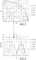
- FIG. 2 illustrates a relationship between the first value ⁇ 1 of the optical splitting ratio and the first value ⁇ 2 of the combining ratio at the different chirps (In the figure, a parameter ⁇ acts as the chirp of the outputting optical signal Oout).
- FIG. 3 illustrates a relationship between the first value ⁇ 1 of the optical splitting ratio and the optical modulation amplitude OMA of the outputting optical signal Oout at the different chirps.
- the optical modulation amplitude OMA of the outputting optical signal Oout has a maximum value. Therefore, by determining the chirp as desired and taking the optical splitting ratio and the combining ratio which corresponds to the chirp and are equal to each other to preset the optical modulating device 1, the present disclosure makes the outputting optical signal Oout have the chirp while make the optical modulation amplitude OMA maximized, to improve optical link budget.
- a second embodiment of the optical modulating device 1 of the present disclosure is similar to the first embodiment, but has a difference in that, in the second embodiment: (1) both the optical splitting ratio and the combining ratio are not constants (that is, are not preset); and (2) the optical modulating device 1 further includes a ratio regulator 14.
- the ratio regulator 14 is used to receive a direct current voltage Vdc which is variable, and adjust the value the optical splitting ratio and the value of the combining ratio according to the direct current voltage Vdc.
- the ratio regulator 14 includes a first electrode 141 and a second electrode 142.
- the first electrode 141 is provided corresponding to and adjacent to the optical splitter 11, and is used to receive the direct current voltage Vdc.
- the second electrode 142 is provided corresponding to and adjacent to the optical combiner 13, and is used to receive the direct current voltage Vdc.
- the first electrode 141 and the second electrode 142 respectively generate heat according to the direct current voltage Vdc, to adjust the value of the optical splitting ratio and the value of the combining ratio to which the first electrode 141 and the second electrode 142 correspond respectively.
- the combining ratio is equal to the optical splitting ratio, the value of the combining ratio is positive number and the value is less than one (1) or more than one (1).
- the optical modulating device 1 of the present disclosure makes the outputting optical signal Oout outputted by the optical modulating device 1 have a larger optical modulation amplitude OMA, makes the outputting optical signal Oout still have a better signal-to-noise ratio when the outputting optical signal Oout is transmitted to the optical receiving device via the optical fiber, so that the optical receiving device has better demodulation accuracy when the optical receiving device demodulates according to the outputting optical signal Oout.
- the outputting optical signal Oout has the optimized chirp in the optical modulating device 1, it may reduce effect of a dispersion caused by the optical fiber on transmission of the outputting optical signal Oout, in turn promote transmission performance of the optical communication system, and increase a transmission distance of the outputting optical signal Oout.
Landscapes
- Physics & Mathematics (AREA)
- Nonlinear Science (AREA)
- General Physics & Mathematics (AREA)
- Optics & Photonics (AREA)
- Engineering & Computer Science (AREA)
- Electromagnetism (AREA)
- Computer Networks & Wireless Communication (AREA)
- Signal Processing (AREA)
- Microelectronics & Electronic Packaging (AREA)
- Optical Modulation, Optical Deflection, Nonlinear Optics, Optical Demodulation, Optical Logic Elements (AREA)
- Optical Communication System (AREA)
Abstract
Description
- The present disclosure relates to a device, and particularly relates to an optical modulating device.
- In optical fiber communication systems, optical fiber dispersion is a phenomenon that optical waves are dispersed into optical spectrum components with different wavelengths due to dependence of wave velocity on wavelength. When an optical signal or pulse emitted by an optical modulating device is projected into, for example, an optical fiber channel, an envelope thereof propagates along the fiber channel at wave group velocities to an optical receiving device. Since this pulse contains a series of optical spectrum components, each optical spectrum component travels at a different wave group velocity, causing group velocity dispersion (GVD), intramodal dispersion or simple optical fiber dispersion. This dispersion phenomenon also is often referred to as pulse broadening. When the pulse travels along the optical fiber, the optical spectrum components continue to be dispersed in space and time, the pulse will become too wide, a front edge of a pulse overlaps a rear edge of a previous pulse, and inter symbol interference (ISI) will occur and the bit will be blurred, which causes that, when the optical receiving device receives the optical signal and demodulate based on the optical signal, the optical receiving device is unable to identify the difference between the "0" bit and the "1" bit and results in demodulation error. In addition, the dispersion of the optical fiber is directly ratio to a length of the optical fiber, that is, a transmission distance of the optical signal is limited by the dispersion of the optical fiber. Moreover, a signal-to-noise ratio (SNR) of the optical signal received by the optical receiving device will also affect demodulation accuracy of the optical receiving device.
- As such, the signal-to-noise ratio and the dispersion of the optical fiber becomes one of the important factors affecting the signal quality of optical fiber communication. Therefore, how to avoid the signal-to-noise ratio being too low and the dispersion of the optical fiber seriously affecting the optical fiber communication system in order to promote the optical transmission distance is a subject to be improved by the relevant communication entities.
- Therefore, an object of the present disclosure is to provide an optical modulating device which can overcome the deficiency of the existing technology.
- Accordingly, an optical modulating device of the present disclosure comprises an optical splitter, an optical phase modulator and an optical combiner. Thee optical splitter is used to receive an inputting optical signal and split the inputting optical signal by an optical splitting ratio to generate a first split optical signal and a second split optical signal. The optical phase modulator couples the optical splitter to receive the first split optical signal and the second split optical signal and phase modulate the first split optical signal and the second split optical signal to respectively generate a first modulating optical signal and a second modulating optical signal. The optical combiner couples the optical phase modulator to receive the first modulating optical signal and the second modulating optical signal and combine the first modulating optical signal and the second modulating optical signal by a combining ratio to generate an outputting optical signal having a chirp, the combining ratio being equal to the optical splitting ratio, a value of the combining ratio being a positive number, and the value being less than one or more than one.
- The effect of the present disclosure lies in that: by that the optical splitting ratio is equal to the optical combining ratio, it makes the outputting optical signal have a better signal-to-noise ratio, so that the optical receiving device has better demodulation accuracy when the optical receiving device receives the outputting optical signal and demodulates according to the outputting optical signal, and the outputting optical signal has the chirp, it may reduce effect of a dispersion caused by the optical fiber on transmission of the outputting optical signal, in turn promote transmission performance of the optical communication system.
- Other features and technical effects of the present disclosure will be apparent in an embodiment referring to the accompanying figures, in which:
-
FIG. 1 is a plan diagram illustrating a first embodiment of an optical modulating device of the present disclosure; -
FIG. 2 is a simulation diagram illustrating that, when a chirp of an outputting optical signal of the first embodiment takes different values, a first value of a combining ratio changes as a first value of an optical splitting ratio; -
FIG. 3 is a simulation diagram illustrating that, when the chirp of the outputting optical signal of the first embodiment takes different values, an optical modulation amplitude of the outputting optical signal changes as the first value of the optical splitting ratio; and -
FIG. 4 is a plan diagram illustrating a second embodiment of the optical modulating device of the present disclosure. - The reference numerals are represented as follows:
- 1 optical modulating device
- 11 optical splitter
- 111, 112 inputting end
- 12 optical phase modulator
- 121 first waveguide
- 122 second waveguide
- 123 first electrode
- 124 second electrode
- 125 bias voltage electrode
- 13 optical combiner
- 131, 132 outputting end
- 14 ratio regulator
- 141 first electrode
- 142 second electrode
- V1 first modulating voltage
- V2 second modulating voltage
- Vb bias voltage signal
- Vdc direct current voltage
- Oin inputting optical signal
- Oout outputting optical signal
- Om1 first modulating optical signal
- Om2 second modulating optical signal
- Os1 first split optical signal
- Os2 second split optical signal
- OMA optical modulation amplitude
- ε1 first value of optical splitting ratio
- ε2 first value of combining ratio
- α chirp
- Before the present disclosure is described in detail, it should be noted that like elements are denoted by the same reference numerals in the following description.
- Referring to
FIG. 1 , an embodiment of an optical modulating device 1 of the present disclosure is adapted to an optical communication system (not shown). The optical communication system includes an optical fiber (not shown) and an optical receiving device (not shown). The optical modulating device 1 is used to modulate an inputting optical signal Oin having a continuous wave, to generate and emit an outputting optical signal Oout having a chirp and transmit the outputting optical signal Oout to the optical receiving device via the optical fiber. The optical receiving device demodulates the outputting optical signal Oout received by the optical receiving device. - The optical modulating device 1 of the present embodiment includes an
optical splitter 11, anoptical phase modulator 12 and anoptical combiner 13. The optical modulating device 1 is a Mach-Zehnder modulator (MZM), the Mach-Zehnder modulator is made of one of a LiNbO3-based, a Silicon and an Inp. - The
optical splitter 11 is used to receive the inputting optical signal Oin, and split the inputting optical signal Oin by an optical splitting ratio (that is, ε1:(1-ε1), 0<ε1<1), to generate a first split optical signal Os1 and a second split optical signal Os2. It is noted that, in the present embodiment, theoptical splitter 11 is an optical directional coupler, and only receives the inputting optical signal Oin, but the present disclosure is not limited thereto. In other embodiments, an inputtingend 111 of theoptical splitter 11 receives the inputting optical signal Oin, and another inputtingend 112 receives another inputting optical signal. Theoptical splitter 11 may be a Y-branch waveguide or a multi-mode interferometer. - The
optical phase modulator 12 couples theoptical splitter 11 to receive the first split optical signal Os1 and the second split optical signal Os2 and phase modulate the first split optical signal Os1 and the second split optical signal Os2, so as to respectively generate a first modulating optical signal Om1 and a second modulating optical signal Om2. In the present embodiment, theoptical phase modulator 12 includes afirst waveguide 121, asecond waveguide 122, afirst electrode 123, asecond electrode 124 and abias voltage electrode 125. - The
first waveguide 121 is coupled between theoptical splitter 11 and theoptical combiner 13, receives the first split optical signal Os1 from theoptical splitter 11, and generates the first modulating optical signal Om1 based on the first split optical signal Os1. Thesecond waveguide 122 is coupled between theoptical splitter 11 and theoptical combiner 13, receives the second split optical signal Os2 from theoptical splitter 11, and generates the second modulating optical signal Om2 based on the second split optical signal Os2. Thefirst electrode 123 is provided corresponding to thefirst waveguide 121, and is used to receive a first modulating voltage V1. Thesecond electrode 124 is provided corresponding to thesecond waveguide 122, and is used to receive a second modulating voltage V2. Specifically, thefirst electrode 123 and thesecond electrode 124 are provided on an upper surface of thefirst waveguide 121 and an upper surface of thesecond waveguide 122 respectively. Thefirst electrode 123 and thesecond electrode 124 cause a refractive index of thefirst waveguide 121 itself and a refractive index of thesecond waveguide 122 itself to generate change respectively according to the first modulating voltage V1 and the second modulating voltage V2 (for example, generate heat according to the first modulating voltage V1 and the second modulating voltage V2 to cause the refractive index of thefirst waveguide 121 and the refractive index of thesecond waveguide 122 to change, but the present disclosure is not limited thereto), to cause a propagating speed of the first split optical signal Os1 propagated by thefirst waveguide 121 and a propagating speed of the second split optical signal Os2 propagated by thesecond waveguide 122 to change (that is, a phase difference is generated between a light propagated in thefirst waveguide 121 and a light propagated in the second waveguide 122 (that is, phase modulate)), and respectively generate the first modulating optical signal Om1 and the second modulating optical signal Om2. As a such, a phase of the first modulating optical signal Om1 and a phase of the second modulating optical signal Om2 change respectively as the first modulating voltage V1 and the second modulating voltage V2 change. - The
bias voltage electrode 125 is provided corresponding to thesecond waveguide 122 and the second electrode 124 (or, thebias voltage electrode 125 is provided corresponding to thefirst waveguide 121 and the first electrode 123), and is used to receive a bias voltage signal Vb. - Specifically, a polarity the chirp of the outputting optical signal Oout is associated with a positive slope or a negative slope of a transfer function of the optical modulating device 1 operated at itself, and a magnitude of the chirp of the outputting optical signal Oout is associated with an offset of a bias voltage point of the optical modulating device 1 from a quadrature point of the transfer function. Therefore, by making the
optical phase modulator 12 controlled by the bias voltage signal Vb, the present embodiment adjusts the optical modulating device 1 to be operated at the positive slope or the negative slope of the transfer function, so as to change the polarity of the chirp, and changes the magnitude of the chirp with making the bias voltage point offset from the quadrature point of the transfer function by the bias voltage signal Vb, , so that the chirp of the outputting optical signal Oout changes as the bias voltage signal Vb changes. - The
optical combiner 13 couples theoptical phase modulator 12 to receive the first modulating optical signal Om1 and the second modulating optical signal Om2, and combine the first modulating optical signal Om1 and the second modulating optical signal Om2 by a combining ratio (that is, ε2:(1-ε2), 0<ε2<1), so as to generate the outputting optical signal Oout. It is noted that, both the combining ratio and the optical splitting ratio are constants. The combining ratio is equal to the optical splitting ratio (that is, ε1:(1-ε1)=ε2:(1-ε2)), a value of the combining ratio is a positive number, and the value is less than one (1) or more than one (1). Moreover, in the present embodiment, theoptical combiner 13 is an optical directional coupler, and only outputs the outputting optical signal Oout, but the present disclosure is not limited thereto. In other embodiments, an outputtingend 131 of theoptical combiner 13 outputs the outputting optical signal Oout, and another outputtingend 132 of theoptical combiner 13 outputs another outputting optical signal. The outputting optical signal Oout and the another outputting optical signal may have different chirps. Theoptical combiner 13 may be a Y-branch waveguide or a multi-mode interferometer. - In the present embodiment, an amplitude of the first modulating voltage V1 and an amplitude of the second modulating voltage V2 are identical, and the phase of the first modulating voltage V1 and the phase of the second modulating voltage V2 differ from each other by180 degrees. An optical modulation amplitude (OMA) of the outputting optical signal Oout may be obtained by the following equation (1):

- Referring to
FIG. 2 and FIG. 3, FIG. 2 illustrates a relationship between the first value ε1 of the optical splitting ratio and the first value ε2 of the combining ratio at the different chirps (In the figure, a parameter α acts as the chirp of the outputting optical signal Oout).FIG. 3 illustrates a relationship between the first value ε1 of the optical splitting ratio and the optical modulation amplitude OMA of the outputting optical signal Oout at the different chirps. As can be seen fromFIG. 2 and FIG. 3 , at the different chirps, when the first value ε1 of the optical splitting ratio is equal to the first value ε2 of the combining ratio (that is, ε1 = ε2), the optical modulation amplitude OMA of the outputting optical signal Oout has a maximum value. Therefore, by determining the chirp as desired and taking the optical splitting ratio and the combining ratio which corresponds to the chirp and are equal to each other to preset the optical modulating device 1, the present disclosure makes the outputting optical signal Oout have the chirp while make the optical modulation amplitude OMA maximized, to improve optical link budget. - Referring to
FIG. 4 , a second embodiment of the optical modulating device 1 of the present disclosure is similar to the first embodiment, but has a difference in that, in the second embodiment: (1) both the optical splitting ratio and the combining ratio are not constants (that is, are not preset); and (2) the optical modulating device 1 further includes aratio regulator 14. - The
ratio regulator 14 is used to receive a direct current voltage Vdc which is variable, and adjust the value the optical splitting ratio and the value of the combining ratio according to the direct current voltage Vdc. In the present embodiment, theratio regulator 14 includes afirst electrode 141 and asecond electrode 142. Thefirst electrode 141 is provided corresponding to and adjacent to theoptical splitter 11, and is used to receive the direct current voltage Vdc. Thesecond electrode 142 is provided corresponding to and adjacent to theoptical combiner 13, and is used to receive the direct current voltage Vdc. Specifically, thefirst electrode 141 and thesecond electrode 142 respectively generate heat according to the direct current voltage Vdc, to adjust the value of the optical splitting ratio and the value of the combining ratio to which thefirst electrode 141 and thesecond electrode 142 correspond respectively. In the present embodiment, similarly, the combining ratio is equal to the optical splitting ratio, the value of the combining ratio is positive number and the value is less than one (1) or more than one (1). - In conclusion, by that the optical splitting ratio is equal to the optical combining ratio, the optical modulating device 1 of the present disclosure makes the outputting optical signal Oout outputted by the optical modulating device 1 have a larger optical modulation amplitude OMA, makes the outputting optical signal Oout still have a better signal-to-noise ratio when the outputting optical signal Oout is transmitted to the optical receiving device via the optical fiber, so that the optical receiving device has better demodulation accuracy when the optical receiving device demodulates according to the outputting optical signal Oout. Moreover, by that the outputting optical signal Oout has the optimized chirp in the optical modulating device 1, it may reduce effect of a dispersion caused by the optical fiber on transmission of the outputting optical signal Oout, in turn promote transmission performance of the optical communication system, and increase a transmission distance of the outputting optical signal Oout.
- However, the above description is only for the embodiments of the present disclosure, and it is not intended to limit the implementing scope of the present disclosure, and the simple equivalent changes and modifications made according to the claims and the contents of the specification are still included in the scope of the present disclosure.
Claims (10)
- An optical modulating device, comprising:an optical splitter which is used to receive an inputting optical signal and split the inputting optical signal by an optical splitting ratio to generate a first split optical signal and a second split optical signal;an optical phase modulator which couples the optical splitter to receive the first split optical signal and the second split optical signal and phase modulate the first split optical signal and the second split optical signal to respectively generate a first modulating optical signal and a second modulating optical signal; andan optical combiner which couples the optical phase modulator to receive the first modulating optical signal and the second modulating optical signal and combine the first modulating optical signal and the second modulating optical signal by a combining ratio to generate an outputting optical signal having a chirp, the combining ratio being equal to the optical splitting ratio, a value of the combining ratio being a positive number, and the value being less than one or more than one.
- The optical modulating device of claim 1, wherein the optical phase modulator comprises:a first waveguide which is coupled between the optical splitter and the optical combiner, receives the first split optical signal from the optical splitter and generates the first modulating optical signal based on the first split optical signal,a second waveguide which is coupled between the optical splitter and the optical combiner, receives the second split optical signal from the optical splitter and generates the second modulating optical signal based on the second split optical signal,a first electrode which is provided corresponding to the first waveguide and is used to receive a first modulating voltage, a phase of the first modulating optical signal changes as the first modulating voltage changes, anda second electrode which is provided corresponding to the second waveguide and is used to receive a second modulating voltage, a phase of the second modulating optical signal changes as the second modulating voltage changes.
- The optical modulating device of claim 2, wherein the chirp is a variable, the optical phase modulator further comprises:
a bias voltage electrode which is provided corresponding to the second waveguide and the second electrode and is used to receive a bias voltage signal, the chirp of the outputting optical signal changes as the bias voltage signal changes. - The optical modulating device of claim 2, wherein the phase of the first modulating voltage and the phase of the second modulating voltage differ from each other by 180 degrees, and an amplitude of the first modulating voltage and an amplitude of the second modulating voltage are identical.
- The optical modulating device of claim 1, wherein the optical splitter and the optical combiner each are a Y-branch waveguide.
- The optical modulating device of claim 1, wherein the optical splitter and the optical combiner each are an optical directional coupler.
- The optical modulating device of claim 1, wherein the optical splitter and the optical combiner each are a multi-mode interferometer.
- The optical modulating device of claim 1, wherein both the optical splitting ratio and the combining ratio are constants.
- The optical modulating device of claim 1, further comprising:
a ratio regulator which is used to receive a direct current voltage which is variable and adjust a value of the optical splitting ratio and a value of the combining ratio according to the direct current voltage. - The optical modulating device of claim 9, wherein the ratio regulator comprises:a first electrode which is provided corresponding to the optical splitter and is used to receive the direct current voltage, anda second electrode which is provided to corresponding to the optical combiner and is used to receive the direct current voltage.
Applications Claiming Priority (1)
| Application Number | Priority Date | Filing Date | Title |
|---|---|---|---|
| CN202010449034.4A CN113721403A (en) | 2020-05-25 | 2020-05-25 | Light modulation device |
Publications (1)
| Publication Number | Publication Date |
|---|---|
| EP3917035A1 true EP3917035A1 (en) | 2021-12-01 |
Family
ID=76011860
Family Applications (1)
| Application Number | Title | Priority Date | Filing Date |
|---|---|---|---|
| EP21174816.5A Withdrawn EP3917035A1 (en) | 2020-05-25 | 2021-05-19 | Optical modulating device |
Country Status (5)
| Country | Link |
|---|---|
| US (2) | US12216377B2 (en) |
| EP (1) | EP3917035A1 (en) |
| JP (1) | JP7221331B2 (en) |
| KR (1) | KR102478968B1 (en) |
| CN (1) | CN113721403A (en) |
Families Citing this family (2)
| Publication number | Priority date | Publication date | Assignee | Title |
|---|---|---|---|---|
| CN114338004B (en) * | 2021-12-11 | 2024-05-10 | 北京量子信息科学研究院 | Modulation device and modulation method for decoy state quantum key distribution system |
| WO2023178517A1 (en) * | 2022-03-22 | 2023-09-28 | 华为技术有限公司 | Optical modulator, emission apparatus, communication system, and modulation method |
Citations (5)
| Publication number | Priority date | Publication date | Assignee | Title |
|---|---|---|---|---|
| US6535653B1 (en) * | 2000-10-06 | 2003-03-18 | Donald J. Lenkszus | Variable chirp optical modulator |
| JP2005252369A (en) * | 2004-03-01 | 2005-09-15 | Nippon Telegr & Teleph Corp <Ntt> | WDM transmission system |
| WO2005096086A1 (en) * | 2004-03-31 | 2005-10-13 | Pirelli & C. S.P.A. | Optical modulator |
| US20080008412A1 (en) * | 2005-03-18 | 2008-01-10 | Fujitsu Limited | Optical device |
| US20090220185A1 (en) * | 2008-02-28 | 2009-09-03 | Oki Semiconductor Co., Ltd. | Light modulating device |
Family Cites Families (10)
| Publication number | Priority date | Publication date | Assignee | Title |
|---|---|---|---|---|
| US5524076A (en) | 1994-01-28 | 1996-06-04 | Northern Telecom Limited | Chirp control of a Mach-Zehnder optical modulator using non-equal power splitting |
| NL1006323C2 (en) * | 1997-06-16 | 1998-12-17 | Mierij Meteo Bv | Integrated optical waveguide system. |
| US7414579B2 (en) | 2004-09-23 | 2008-08-19 | Interdigital Technology Corporation | Blind signal separation using correlated antenna elements |
| JP2008009314A (en) | 2006-06-30 | 2008-01-17 | Arasor Corp | Optical waveguide element, optical modulator, and optical communication device |
| JP2012519873A (en) | 2009-03-03 | 2012-08-30 | オクラロ テクノロジー リミテッド | Improved optical waveguide splitter |
| JP2014219571A (en) | 2013-05-08 | 2014-11-20 | 富士通オプティカルコンポーネンツ株式会社 | Optical modulation control apparatus, transmitter, and optical output waveform control method |
| TWI515477B (en) | 2013-07-26 | 2016-01-01 | High - speed optical modulation device | |
| US9590730B2 (en) | 2014-10-01 | 2017-03-07 | Futurewei Technologies, Inc. | Optical transmitter with optical receiver-specific dispersion pre-compensation |
| JP6661519B2 (en) | 2016-02-19 | 2020-03-11 | 三菱電機株式会社 | Optical transmitter |
| US10547408B2 (en) | 2018-05-03 | 2020-01-28 | Juniper Networks, Inc. | Methods and apparatus for improving the skew tolerance of a coherent optical transponder in an optical communication system |
-
2020
- 2020-05-25 CN CN202010449034.4A patent/CN113721403A/en active Pending
-
2021
- 2021-05-19 EP EP21174816.5A patent/EP3917035A1/en not_active Withdrawn
- 2021-05-24 JP JP2021086928A patent/JP7221331B2/en active Active
- 2021-05-25 US US17/329,206 patent/US12216377B2/en active Active
- 2021-05-25 KR KR1020210066622A patent/KR102478968B1/en active Active
-
2024
- 2024-12-27 US US19/002,772 patent/US20250123533A1/en active Pending
Patent Citations (5)
| Publication number | Priority date | Publication date | Assignee | Title |
|---|---|---|---|---|
| US6535653B1 (en) * | 2000-10-06 | 2003-03-18 | Donald J. Lenkszus | Variable chirp optical modulator |
| JP2005252369A (en) * | 2004-03-01 | 2005-09-15 | Nippon Telegr & Teleph Corp <Ntt> | WDM transmission system |
| WO2005096086A1 (en) * | 2004-03-31 | 2005-10-13 | Pirelli & C. S.P.A. | Optical modulator |
| US20080008412A1 (en) * | 2005-03-18 | 2008-01-10 | Fujitsu Limited | Optical device |
| US20090220185A1 (en) * | 2008-02-28 | 2009-09-03 | Oki Semiconductor Co., Ltd. | Light modulating device |
Non-Patent Citations (3)
| Title |
|---|
| ANDRE P S ET AL: "OPTIMISING THE OPERATION CHARACTERISTICS OF A LINBO3 BASED MACH-ZEHNDER MODULATOR FOR 10 GBIT/S LIGHTWAVE SYSTEMS", JOURNAL OF OPTICAL COMMUNICATIONS, FACHVERLAG SCHIELE & SCHON, BERLIN, DE, vol. 23, no. 6, 1 December 2002 (2002-12-01), pages 234 - 238, XP001227158, ISSN: 0173-4911 * |
| CARTLEDGE J C: "Performance of 10 Gb/s lightwave systems based on lithium niobate Mach-Zehnder modulators with asymmetric Y-branch waveguides", IEEE PHOTONICS TECHNOLOGY LETTERS, IEEE, USA, vol. 7, no. 9, 1 September 1995 (1995-09-01), pages 1090 - 1092, XP011432922, ISSN: 1041-1135, DOI: 10.1109/68.414712 * |
| CHRIS LAWETZ ET AL: "Modulation Characteristics of Semiconductor Mach-Zehnder Optical Modulators", JOURNAL OF LIGHTWAVE TECHNOLOGY, IEEE, USA, vol. 15, no. 4, 1 April 1997 (1997-04-01), XP011028810, ISSN: 0733-8724 * |
Also Published As
| Publication number | Publication date |
|---|---|
| CN113721403A (en) | 2021-11-30 |
| KR102478968B1 (en) | 2022-12-19 |
| US20250123533A1 (en) | 2025-04-17 |
| JP7221331B2 (en) | 2023-02-13 |
| KR20210145687A (en) | 2021-12-02 |
| US12216377B2 (en) | 2025-02-04 |
| JP2021189446A (en) | 2021-12-13 |
| US20210364879A1 (en) | 2021-11-25 |
Similar Documents
| Publication | Publication Date | Title |
|---|---|---|
| US20250123533A1 (en) | Method for modulating signal quality of an optical modulation communication system | |
| JP3433753B2 (en) | Tunable chirped light modulator using a single modulation source | |
| US6721081B1 (en) | Variable duty cycle optical pulses | |
| EP2042913A2 (en) | Optical quaternary phase modulator | |
| US8184355B2 (en) | Light modulation device | |
| US10901153B2 (en) | Null bias mach-zehnder interferometer with ring resonators | |
| US9485032B2 (en) | Optical multilevel transmitter and optical transponder | |
| EP2058690A1 (en) | Optical modulator | |
| EP1304820A1 (en) | Optical transmitter and optical fiber transmission system having the same | |
| US8693887B2 (en) | Optical transmitter and optical transmission system | |
| JP4527993B2 (en) | Light modulation apparatus and light modulation method | |
| US11942993B2 (en) | Optical transmission device and optical communication system | |
| US7660027B2 (en) | Optical modulator and modulation method | |
| JP5198996B2 (en) | Light modulator | |
| JP2008244514A (en) | Optical transmitter and relay node for reducing in-phase crosstalk between WDM channels | |
| JP2679223B2 (en) | Optical modulation method and optical modulator | |
| US7155071B2 (en) | Device for Mach-Zehnder modulator bias control for duobinary optical transmission and associated system and method | |
| US20110075149A1 (en) | Optical receiver | |
| US10425166B2 (en) | Optical transmitter, optical transmission apparatus, and optical modulation method | |
| TWI762933B (en) | light modulation device | |
| JP2010219779A (en) | Optical signal transmitter in wavelength division multiplex transmission | |
| US8064778B2 (en) | Method and apparatus for controlling tunable transmitter chirp | |
| US20240219754A1 (en) | Optical Modulator and Digital Signal Processing Method | |
| AHMED | Implementation of Differential Modulation Techniques to Increase the Capacity of Optical Communication Systems |
Legal Events
| Date | Code | Title | Description |
|---|---|---|---|
| PUAI | Public reference made under article 153(3) epc to a published international application that has entered the european phase |
Free format text: ORIGINAL CODE: 0009012 |
|
| STAA | Information on the status of an ep patent application or granted ep patent |
Free format text: STATUS: THE APPLICATION HAS BEEN PUBLISHED |
|
| AK | Designated contracting states |
Kind code of ref document: A1 Designated state(s): AL AT BE BG CH CY CZ DE DK EE ES FI FR GB GR HR HU IE IS IT LI LT LU LV MC MK MT NL NO PL PT RO RS SE SI SK SM TR |
|
| B565 | Issuance of search results under rule 164(2) epc |
Effective date: 20211025 |
|
| STAA | Information on the status of an ep patent application or granted ep patent |
Free format text: STATUS: REQUEST FOR EXAMINATION WAS MADE |
|
| 17P | Request for examination filed |
Effective date: 20220413 |
|
| RBV | Designated contracting states (corrected) |
Designated state(s): AL AT BE BG CH CY CZ DE DK EE ES FI FR GB GR HR HU IE IS IT LI LT LU LV MC MK MT NL NO PL PT RO RS SE SI SK SM TR |
|
| STAA | Information on the status of an ep patent application or granted ep patent |
Free format text: STATUS: EXAMINATION IS IN PROGRESS |
|
| 17Q | First examination report despatched |
Effective date: 20230612 |
|
| P01 | Opt-out of the competence of the unified patent court (upc) registered |
Effective date: 20230528 |
|
| STAA | Information on the status of an ep patent application or granted ep patent |
Free format text: STATUS: THE APPLICATION HAS BEEN WITHDRAWN |
|
| 18W | Application withdrawn |
Effective date: 20251112 |