EP3917020A1 - Signal transceiving apparatus and terminal device - Google Patents
Signal transceiving apparatus and terminal device Download PDFInfo
- Publication number
- EP3917020A1 EP3917020A1 EP20744687.3A EP20744687A EP3917020A1 EP 3917020 A1 EP3917020 A1 EP 3917020A1 EP 20744687 A EP20744687 A EP 20744687A EP 3917020 A1 EP3917020 A1 EP 3917020A1
- Authority
- EP
- European Patent Office
- Prior art keywords
- transmitting
- receiving
- port
- switch
- antenna
- Prior art date
- Legal status (The legal status is an assumption and is not a legal conclusion. Google has not performed a legal analysis and makes no representation as to the accuracy of the status listed.)
- Granted
Links
Images


Classifications
-
- H—ELECTRICITY
- H04—ELECTRIC COMMUNICATION TECHNIQUE
- H04B—TRANSMISSION
- H04B1/00—Details of transmission systems, not covered by a single one of groups H04B3/00 - H04B13/00; Details of transmission systems not characterised by the medium used for transmission
- H04B1/005—Details of transmission systems, not covered by a single one of groups H04B3/00 - H04B13/00; Details of transmission systems not characterised by the medium used for transmission adapting radio receivers, transmitters andtransceivers for operation on two or more bands, i.e. frequency ranges
- H04B1/0053—Details of transmission systems, not covered by a single one of groups H04B3/00 - H04B13/00; Details of transmission systems not characterised by the medium used for transmission adapting radio receivers, transmitters andtransceivers for operation on two or more bands, i.e. frequency ranges with common antenna for more than one band
- H04B1/006—Details of transmission systems, not covered by a single one of groups H04B3/00 - H04B13/00; Details of transmission systems not characterised by the medium used for transmission adapting radio receivers, transmitters andtransceivers for operation on two or more bands, i.e. frequency ranges with common antenna for more than one band using switches for selecting the desired band
-
- H—ELECTRICITY
- H04—ELECTRIC COMMUNICATION TECHNIQUE
- H04B—TRANSMISSION
- H04B1/00—Details of transmission systems, not covered by a single one of groups H04B3/00 - H04B13/00; Details of transmission systems not characterised by the medium used for transmission
- H04B1/02—Transmitters
- H04B1/04—Circuits
- H04B1/0483—Transmitters with multiple parallel paths
-
- H—ELECTRICITY
- H04—ELECTRIC COMMUNICATION TECHNIQUE
- H04B—TRANSMISSION
- H04B1/00—Details of transmission systems, not covered by a single one of groups H04B3/00 - H04B13/00; Details of transmission systems not characterised by the medium used for transmission
- H04B1/06—Receivers
- H04B1/16—Circuits
- H04B1/1607—Supply circuits
- H04B1/1615—Switching on; Switching off, e.g. remotely
-
- H—ELECTRICITY
- H04—ELECTRIC COMMUNICATION TECHNIQUE
- H04B—TRANSMISSION
- H04B1/00—Details of transmission systems, not covered by a single one of groups H04B3/00 - H04B13/00; Details of transmission systems not characterised by the medium used for transmission
- H04B1/38—Transceivers, i.e. devices in which transmitter and receiver form a structural unit and in which at least one part is used for functions of transmitting and receiving
- H04B1/40—Circuits
-
- H—ELECTRICITY
- H04—ELECTRIC COMMUNICATION TECHNIQUE
- H04B—TRANSMISSION
- H04B1/00—Details of transmission systems, not covered by a single one of groups H04B3/00 - H04B13/00; Details of transmission systems not characterised by the medium used for transmission
- H04B1/38—Transceivers, i.e. devices in which transmitter and receiver form a structural unit and in which at least one part is used for functions of transmitting and receiving
- H04B1/40—Circuits
- H04B1/44—Transmit/receive switching
-
- H—ELECTRICITY
- H04—ELECTRIC COMMUNICATION TECHNIQUE
- H04B—TRANSMISSION
- H04B7/00—Radio transmission systems, i.e. using radiation field
- H04B7/02—Diversity systems; Multi-antenna system, i.e. transmission or reception using multiple antennas
- H04B7/04—Diversity systems; Multi-antenna system, i.e. transmission or reception using multiple antennas using two or more spaced independent antennas
- H04B7/06—Diversity systems; Multi-antenna system, i.e. transmission or reception using multiple antennas using two or more spaced independent antennas at the transmitting station
- H04B7/0686—Hybrid systems, i.e. switching and simultaneous transmission
- H04B7/0691—Hybrid systems, i.e. switching and simultaneous transmission using subgroups of transmit antennas
-
- H—ELECTRICITY
- H04—ELECTRIC COMMUNICATION TECHNIQUE
- H04B—TRANSMISSION
- H04B7/00—Radio transmission systems, i.e. using radiation field
- H04B7/02—Diversity systems; Multi-antenna system, i.e. transmission or reception using multiple antennas
- H04B7/04—Diversity systems; Multi-antenna system, i.e. transmission or reception using multiple antennas using two or more spaced independent antennas
- H04B7/08—Diversity systems; Multi-antenna system, i.e. transmission or reception using multiple antennas using two or more spaced independent antennas at the receiving station
- H04B7/0868—Hybrid systems, i.e. switching and combining
- H04B7/0874—Hybrid systems, i.e. switching and combining using subgroups of receive antennas
Definitions
- the present disclosure relates to the field of communication technologies, and in particular, to a signal transceiving apparatus and a terminal device.
- users have more and more requirements for mobile communication technologies. For example, users require for high reliability and a low latency to meet applications requirements of Internet of Vehicles, autonomous driving, telemedicine, and the like; users require for a higher communication rate to support an application requirement of ultra-high-definition videos; users require for low power consumption, large-connection scenarios, high traffic density, and the like to meet the requirements for widespread coverage of the Internet of Things and hotspot communication in smart industry and agriculture, and the like. To meet these requirements, the fifth-generation (5G for short) mobile communication technology appears.
- 5G fifth-generation
- 5G introduces a new broadband spectrum, for example, a millimeter wave band and a band below 6G (sub 6G for short) meet broadband high-speed and low-latency coverage requirements, where sub 6G is divided into bands of 3.5 GHz (3.3 GHz to 4.2 GHz) and 4.5 GHz (4.4 GHz to 5.0 GHz).
- sub 6G is divided into bands of 3.5 GHz (3.3 GHz to 4.2 GHz) and 4.5 GHz (4.4 GHz to 5.0 GHz).
- a large-scale antenna technology, multiple access, beamforming, high-power terminal, and other technologies are further used to meet the above needs.
- the 5G spectrum is planned as follows: Band number Uplink frequency (MHZ) Downlink frequency (MHZ) Duplex mode n1 1920-1980 2110-2170 Frequency division duplex n2 1850-1910 1930-1990 Frequency division duplex n3 1710-1785 1805-1880 Frequency division duplex n5 824-849 869-894 Frequency division duplex n7 2500-2570 2620-2690 Frequency division duplex n8 880-915 925-960 Frequency division duplex n20 832-862 791-821 Frequency division duplex n28 703-748 758-803 Frequency division duplex n38 2570-2620 2570-2621 Time division duplex n41 2496-2690 2496-2691 Time division duplex n50 1432-1517 1432-1517 Time division duplex n51 1427-1432 1427-1432 Time division duplex n66 1710-1780 2110-2200 Frequency division duplex n70 1695-1710 1995-
- the newly added sub 6G bands of 5G that is, the n77, n78, and n79 bands all use time division duplexing (Time Division Duplexing, TDD) mode. Therefore, the proportion of TDD in 5G will increase, and more attention will be paid to the application of TDD.
- n1, n2, n3, n5, n7, n8, n38, n41, and other bands are all refarming (spectrum redeployment) bands of long term evolution (Long Term Evolution, LTE). Therefore, 4G and 5G will coexist for a long time.
- the terminal products tend to be lightweight and portable.
- the compatible solution of 1T4R and 2T4R has a complex design architecture, use immature materials such as 3P3T (the larger the number of T, the worse the performance), and the wire is long, which affects the overall transmitting and receiving performance.
- Performance of 3P3T or 4P4T is worse than that of double-pole-double-throw (double-pole-double-throw, DPDT) switch, resulting in a large overall loss on a receiving channel.
- DPDT double-pole-double-throw
- the costs are much higher than those of the DPDT.
- the embodiments of the present disclosure provide a signal transceiving apparatus and a terminal device to solve the problem that a radio frequency transceiving system has a complex structure and a long wire, which affects transmitting and receiving performance, and causes high complexity of design and high costs of terminal products in the related technology.
- an embodiment of the present disclosure provides a signal transceiving apparatus, including:
- an embodiment of this disclosure provides a terminal device, including the signal transceiving apparatus.
- the first terminal of the first communication module and the first terminal of the second communication module are respectively connected to the first switch, the second switch is disposed between the second terminal of the first communication module and the first antenna structure, and the third switch is disposed between the second terminal of the second communication module and the second antenna structure.
- the structural design can reduce insertion loss of the receiving link, improve performance of the transmitting link, shorten a wire length, and reduce the design complexity of the terminal device and reduce manufacturing costs.
- An embodiment of the present disclosure provides a signal transceiving apparatus. As shown in FIG.
- the apparatus includes: a first communication module 11 and a second communication module 12; a first switch 2 connected to a first terminal of the first communication module 11 and a first terminal of the second communication module 12, respectively; a second switch 31 connected to a second terminal of the first communication module 11, and a first antenna structure 4 connected to the second switch 31; and a third switch 32 connected to a second terminal of the second communication module 12, and a second antenna structure 5 connected to the third switch 32.
- the first communication module 11 corresponds to a first transmitting link and two receiving links
- the second communication module 12 corresponds to a second transmitting link and two receiving links; in a case of signal transmission, at least one of the first transmitting link and the second transmitting link is in a conductive state, and in a case of signal reception, the two receiving links corresponding to the first communication module 11 and the two receiving links corresponding to the second communication module 12 are all in a conductive state.
- the signal transceiving apparatus includes: the first communication module 11, the second communication module 12, the first switch 2, the second switch 31, the third switch 32, the first antenna structure 4, and the second antenna structure 5.
- the first terminal of the first communication module 11 and the first terminal of the second communication module 12 are both connected to the first switch 2, the second terminal of the first communication module 11 is connected to the first antenna structure 4 through the second switch 31, and the second terminal of the second communication module 12 is connected to the second antenna structure 5 through the third switch 32.
- the first communication module 11 corresponds to a first transmitting link and two receiving links
- the second communication module 12 corresponds to a second transmitting link and two receiving links; in a case of signal transmission, the first transmitting link of the first communication module 11 and/or the second transmitting link of the second communication module 12 is conducted, and in a case of signal reception, the two receiving links of the first communication module 11 and the two receiving links of the second communication module 12 are all conducted.
- the mode of transmitting by using one link and receiving by using four links (1T4R) may be implemented.
- the mode of transmitting by using two links and receiving by using four links (2T4R) may be implemented.
- the signal transceiving apparatus of the present disclosure can ensure the compatibility between two modes of transmitting by using one link and receiving by using four links and transmitting by using two links and receiving by using four links.
- the structural design can reduce insertion loss of the receiving link, improve performance of the transmitting link, shorten a wire length, and reduce the design complexity of the terminal device and reduce manufacturing costs.
- the first switch 2, the second switch 31, and the third switch 32 are all double-pole-double-throw switches.
- the signal transceiving apparatus further includes: a modem 6. A first terminal of the first switch 2 is connected to a first port and a second port of the modem 6, and a second terminal of the first switch 2 is connected to a first transmitting port 111 of the first communication module 11 and a second transmitting port 121 of the second communication module 12.
- the first switch 2 is a double-pole-double-throw switch, the first switch 2 may be connected to the first communication module 11 and the second communication module 12, and the first terminal of the first switch 2 is connected to the modem 6, and specifically connected to the first port and the second port of the modem 6.
- the first port and the second port are both transmitting ports.
- the first communication module 11 includes the first transmitting port 111
- the second communication module 12 includes the second transmitting port 121.
- the first transmitting port 111 is located at the first terminal of the first communication module 11, the second transmitting port 121 is located at the first terminal of the second communication module 12.
- the second terminal of the first switch 2 is connected to the first transmitting port 111 of the first communication module 11 and the second transmitting port 121 of the second communication module 12.
- the first transmitting port 111 may be connected to the first non-movable terminal of the first switch 2, the second transmitting port 121 is connected to the second non-movable terminal of the first switch 2, the first movable terminal of the first switch 2 is connected to the first port of the modem 6, and the second movable terminal of the first switch 2 is connected to the second port of the modem 6.
- the first movable terminal of the first switch 2 may be connected to the first non-movable terminal, and the second movable terminal may be connected to the second non-movable terminal, so that the first transmitting port 111 is connected to the first port of the modem 6, and the second transmitting port 121 is connected to the second port of the modem 6.
- the first movable terminal of the first switch 2 may be connected to the second non-movable terminal, and the second movable terminal may be connected to the first non-movable terminal, so that the first transmitting port 111 is connected to the second port of the modem 6, and the second transmitting port 121 is connected to the first port of the modem 6.
- the modem 6 may be connected to a baseband processor.
- the modem 6 converts a baseband signal transmitted by the baseband processor into a radio frequency signal, and sends the radio frequency signal through the first transmitting link and/or the second transmitting link; and in a case of signal reception, converts a received radio frequency signal into a baseband signal and transmits the baseband signal to the baseband processor, to implement processing of signal transmission and signal reception.
- a first terminal of the second switch 31 is connected to a first transmitting/receiving port 112 and a first signal reception port 113 of the first communication module 11, and a second terminal of the second switch 31 is connected to a first antenna 41 and a second antenna 42 of the first antenna structure 4.
- the first communication module 11 includes the first transmitting/receiving port 112 and the first signal reception port 113 located at the second terminal
- the first antenna structure 4 includes the first antenna 41 and the second antenna 42
- the second switch 31 is disposed between the first communication module 11 and the first antenna structure 4.
- a first terminal of the second switch 31 may be connected to a first transmitting/receiving port 112 and a first signal reception port 113
- a second terminal of the second switch 31 is connected to a first antenna 41 and a second antenna 42.
- the first transmitting/receiving port 112 is connected to the first movable terminal of the second switch 31, the first signal reception port 113 is connected to the second movable terminal of the second switch 31, and the first non-movable terminal and the second non-movable terminal of the second switch 31 are connected to the first antenna 41 and the second antenna 42 of the first antenna structure 4.
- the first movable terminal of the second switch 31 may be connected to the first non-movable terminal, and the second movable terminal of the second switch 31 may be connected to the second non-movable terminal, so that the first transmitting/receiving port 112 is connected to the first antenna 41, and the first signal reception port 113 is connected to the second antenna 42.
- the first movable terminal of the second switch 31 further may be connected to the second non-movable terminal, and the second movable terminal may be connected to the first non-movable terminal, so that the first transmitting/receiving port 112 is connected to the second antenna 42, and the first signal reception port 113 is connected to the first antenna 41.
- the first transmitting/receiving port 112 may be connected to the first antenna 41, and the first signal reception port 113 may be connected to the second antenna 42 by the second switch 31, or the first transmitting/receiving port 112 may be connected to the second antenna 42, and the first signal reception port 113 may be connected to the first antenna 41 by the second switch 31.
- a first terminal of the third switch 32 is connected to 12 a second transmitting/receiving port 122 and a second signal reception port 123 of the second communication module, and a second terminal of the third switch 32 is connected to a third antenna 51 and a fourth antenna 52 of the second antenna structure 5.
- the second communication module 12 includes the second transmitting/receiving port 122 and the second signal reception port 123 located at the second terminal, the second antenna structure 5 includes the third antenna 51 and the fourth antenna 52, and the third switch 32 is disposed between the second communication module 12 and the second antenna structure 5.
- the third switch 32 is a double-pole-double-throw switch, a first terminal of the third switch 32 may be connected to a second transmitting/receiving port 122 and a second signal reception port 123, and a second terminal of the third switch 32 is connected to a third antenna 51 and a fourth antenna 52.
- the second transmitting/receiving port 122 is connected to the first movable terminal of the third switch 32, the second signal reception port 123 is connected to the second movable terminal of the third switch 32, and the first non-movable terminal and the second non-movable terminal of the third switch 32 are connected to the third antenna 51 and the fourth antenna 52 of the second antenna structure 5.
- the first movable terminal of the third switch 32 may be connected to the first non-movable terminal, and the second movable terminal of the third switch 32 may be connected to the second non-movable terminal, so that the second transmitting/receiving port 122 is connected to the third antenna 51, and the second signal reception port 123 is connected to the fourth antenna 52.
- the first movable terminal of the third switch 32 further may be connected to the second non-movable terminal, and the second movable terminal may be connected to the first non-movable terminal, so that the second transmitting/receiving port 122 is connected to the fourth antenna 52, and the second signal reception port 123 is connected to the third antenna 51.
- the second transmitting/receiving port 122 is connected to the third antenna 51, and the second signal reception port 123 is connected to the fourth antenna 52 by the third switch 32, or the second transmitting/receiving port 122 is connected to the fourth antenna 52, and the second signal reception port 123 is connected to the third antenna 51 by the third switch 32.
- the mature double-pole-double-throw switch with advantages in both insertion loss and isolation is used to replace the 3P3T disposed between the communication module and the antenna structure, which can reduce insertion loss of a receiving path and reduce costs.
- the double-pole-double-throw switch is added before the transmitting link (between the communication module and the modem), which can eliminate the insertion loss and load impact, improve the transmitting performance, and shorten the wire length.
- this can achieve compatibility between two modes of transmitting by using one link and receiving by using four links and transmitting by using two links and receiving by using four links, and reduce the complexity of design of a radio frequency link.
- the first communication module 11 further includes: the first power amplifier 114, the first transmitting/receiving filter 115, the first receiving filter 116, the first transmission port 117, the second transmission port 118, and the first single-pole-double-throw switch 119.
- the first power amplifier 114 is connected to the first transmitting port 111, the first transmitting/receiving filter 115 is connected to the first transmitting/receiving port 112, a first non-movable terminal of the first single-pole-double-throw switch 119 is connected to the first power amplifier 114, a second non-movable terminal of the first single-pole-double-throw switch 119 is connected to the first transmission port 117, a movable terminal of the first single-pole-double-throw switch 119 is connected to the first transmitting/receiving filter 115, the second transmission port 118 is connected to the first signal reception port 113 through the first receiving filter 116, and the first transmission port 117 and the second transmission port 118 are both connected to a receiving port of the modem 6.
- the first communication module 11 further includes: a first power amplifier 114 for power amplification connected to the first transmitting port 111, a first transmitting/receiving filter 115 for transmitting and receiving multiplexing connected to the first transmitting/receiving port 112, a first transmission port 117 and a second transmission port 118 located at the same terminal as that of the first transmitting port 111, a first receiving filter 116 disposed between the second transmission port 118 and the first signal reception port 113 and connected to the second transmission port 118 and the first signal reception port 113, and a first single-pole-double-throw switch 119 for switching between transmitting and receiving links.
- a first power amplifier 114 for power amplification connected to the first transmitting port 111
- a first transmitting/receiving filter 115 for transmitting and receiving multiplexing connected to the first transmitting/receiving port 112
- a first transmission port 117 and a second transmission port 118 located at the same terminal as that of the first transmitting port 111
- the first transmitting/receiving filter 115 may be connected to the first power amplifier 114, or the first transmitting/receiving filter 115 may be connected to the first transmission port 117.
- the first transmission port 117 and the second transmission port 118 are receiving ports, and are both connected to the receiving port of the modem 6 to transmit a received radio frequency signal to the modem 6.
- the movable terminal and the first non-movable terminal of the first single-pole-double-throw switch 119 are connected.
- the first single-pole-double-throw switch 119 connects the first power amplifier 114 to the first transmitting/receiving filter 115.
- the modem 6, the first switch 2, the first transmitting port 111, the first power amplifier 114, the first single-pole-double-throw switch 119, the first transmitting/receiving filter 115, the first transmitting/receiving port 112, the second switch 31, and a first transmitting antenna are connected in sequence, and the first transmitting antenna is the first antenna 41 or the second antenna 42.
- the first single-pole-double-throw switch 119 connects the first power amplifier 114 to the first transmitting/receiving filter 115, the modem 6, the first switch 2, the first transmitting port 111, the first power amplifier 114, the first single-pole-double-throw switch 119, the first transmitting/receiving filter 115, the first transmitting/receiving port 112, the second switch 31, and a first transmitting antenna are connected, so that the first transmitting link may be formed.
- the first communication module 11 corresponds to the first receiving link and the second receiving link.
- the movable terminal of the first single-pole-double-throw switch 119 is connected to the second non-movable terminal, a first receiving antenna, the second switch 31, the first transmitting/receiving port 112, the first transmitting/receiving filter 115, the first single-pole-double-throw switch 119, the first transmission port 117, and the modem 6 are connected in sequence.
- a second receiving antenna, the second switch 31, the first signal reception port 113, the first receiving filter 116, the second transmission port 118, and the modem 6 are connected in sequence.
- Each of the first receiving antenna and the second receiving antenna is one of the first antenna 41, the second antenna 42.
- the first single-pole-double-throw switch 119 connects the first transmission port 117 to the first transmitting/receiving filter 115, the first receiving antenna, the second switch 31, the first transmitting/receiving port 112, the first transmitting/receiving filter 115, the first single-pole-double-throw switch 119, the first transmission port 117, and the modem 6 are connected, so that the first receiving link may be formed.
- the second receiving antenna, the second switch 31, the first signal reception port 113, the first receiving filter 116, the second transmission port 118, and the modem 6 are connected in sequence; and are always in a conductive state, so that the second receiving link may be formed.
- the first power amplifier 114 may be in an off state.
- Each of the first receiving antenna and the second receiving antenna is one of the first antenna 41 and the second antenna 42, that is, in a case that the first receiving antenna is the first antenna 41, the second receiving antenna is the second antenna 42.
- the second receiving antenna is the first antenna 41.
- the second communication module 12 further includes: a second power amplifier 124, a second transmitting/receiving filter 125, a second receiving filter 126, a third transmission port 127, a fourth transmission port 128, and a second single-pole-double-throw switch 129; where the second power amplifier 124 is connected to the second transmitting port 121, the second transmitting/receiving filter 125 is connected to the second transmitting/receiving port 122, a first non-movable terminal of the second single-pole-double-throw switch 129 is connected to the second power amplifier 124, a second non-movable terminal of the second single-pole-double-throw switch 129 is connected to the third transmission port 127, a movable terminal of the second single-pole-double-throw switch 129 is connected to the second transmitting/receiving filter 125, the fourth transmission port 128 is connected to the second signal reception port 123 through the second receiving filter 126
- the second communication module 12 further includes: a second power amplifier 124 for power amplification connected to the second transmitting port 121, a second transmitting/receiving filter 125 for transmitting and receiving multiplexing connected to the second transmitting/receiving port 122, a third transmission port 127 and a fourth transmission port 128 located at the same terminal as the second transmitting port 121, a second receiving filter 126 disposed between the fourth transmission port 128 and the second signal reception port 123 and connected to the fourth transmission port 128 and the second signal reception port 123, and a second single-pole-double-throw switch 129 for switching a transmitting and receiving link.
- a second power amplifier 124 for power amplification connected to the second transmitting port 121
- a second transmitting/receiving filter 125 for transmitting and receiving multiplexing connected to the second transmitting/receiving port 122
- a third transmission port 127 and a fourth transmission port 128 located at the same terminal as the second transmitting port 121
- Two non-movable terminals of the second single-pole-double-throw switch 129 are connected to the second power amplifier 124 and the third transmission port 127, and the movable terminal of the second single-pole-double-throw switch 129 is connected to the second transmitting/receiving filter 125.
- the second transmitting/receiving filter 125 may be connected to the second power amplifier 124, or the second transmitting/receiving filter 125 may be connected to the third transmission port 127.
- the third transmission port 127 and the fourth transmission port 128 are receiving ports, and are both connected to the receiving port of the modem 6, to transmit a received radio frequency signal to the modem 6.
- the movable terminal and the first non-movable terminal of the second single-pole-double-throw switch 129 are connected, the modem 6, the first switch 2, the second transmitting port 121, the second power amplifier 124, the second single-pole-double-throw switch 129, the second transmitting/receiving filter 125, the second transmitting/receiving port 122, the third switch 32, and a second transmitting antenna are connected in sequence, and the second transmitting antenna is the third antenna 51 or the fourth antenna 52.
- the second single-pole-double-throw switch 129 connects the second power amplifier 124 to the second transmitting/receiving filter 125, the modem 6, the first switch 2, the second transmitting port 121, the second power amplifier 124, the second single-pole-double-throw switch 129, the second transmitting/receiving filter 125, the second transmitting/receiving port 122, the third switch 32, and a second transmitting antenna are connected, so that the second transmitting link may be formed.
- the second communication module 12 corresponds to the third receiving link and the fourth receiving link.
- the movable terminal of the second single-pole-double-throw switch 129 is connected to the second non-movable terminal, a third receiving antenna, the third switch 32, the second transmitting/receiving port 122, the second transmitting/receiving filter 125, the second single-pole-double-throw switch 129, the third transmission port 127, and the modem 6 are connected in sequence.
- a fourth receiving antenna, the third switch 32, the second signal reception port 123, the second receiving filter 126, the fourth transmission port 128, and the modem 6 are connected in sequence.
- Each of the third receiving antenna and the fourth receiving antenna is one of the third antenna 51 and the fourth antenna 52.
- the second single-pole-double-throw switch 129 connects the third transmission port 127 to the second transmitting/receiving filter 125, the third receiving antenna, the third switch 32, the second transmitting/receiving port 122, the second transmitting/receiving filter 125, the second single-pole-double-throw switch 129, the third transmission port 127, and the modem 6 are connected, so that the third receiving link may be formed.
- the fourth receiving antenna, the third switch 32, the second signal reception port 123, the second receiving filter 126, the fourth transmission port 128, and the modem 6 are connected in sequence; and are always in a conductive state, so that the fourth receiving link may be formed.
- the second power amplifier 124 may be in an off state.
- the fourth receiving antenna is the fourth antenna 52.
- the fourth receiving antenna is the third antenna 51.
- the first communication module 11 and the second communication module 12 are both 5G communication modules, which may realize compatibility of two modes of transmitting by using one link and receiving by using four links and transmitting by using two links and receiving by using four links in 4G and 5G coexistence mode and 5G large-scale access. This reduces the design complexity of the terminal device, improves performance, and reduces manufacturing costs.
- the first communication module 11 and the second communication module 12 may be communication circuits or communication chips.
- the first terminal of the first communication module and the first terminal of the second communication module are respectively connected to the first switch, the second switch is disposed between the second terminal of the first communication module and the first antenna structure, and the third switch is disposed between the second terminal of the second communication module and the second antenna structure.
- connection states of the three switches in a case of signal transmission, at least one of the first transmitting link corresponding to the first communication module and the second transmitting link corresponding to the second communication module is in a conductive state.
- the two receiving links corresponding to the first communication module and the two receiving links corresponding to the second communication module are all in a conductive state.
- the structural design can reduce insertion loss of the receiving link, improve performance of the transmitting link, shorten a wire length, and reduce the design complexity of the terminal device and reduce manufacturing costs.
- An embodiment of this disclosure further provides a terminal device, including the signal transceiving apparatus.
- the terminal device further includes a processor 7, which is connected to the signal transceiving apparatus, and may control the operation of the signal transceiving apparatus.
- the processor 7 is specifically connected to the first switch 2, the second switch 31, the third switch 32, the first communication module 11, and the second communication module 12 of the signal transceiving apparatus.
- the processor 7 may determine the first transmitting antenna in the first antenna 41 and the second antenna 42, and determine the second transmitting antenna in the third antenna 51 and the fourth antenna 52 according to an environmental reference signal.
- the processor 7 may determine the transmitting antenna in the first antenna 41, the second antenna 42, the third antenna 51, and the fourth antenna 52 according to an environmental reference signal.
- the processor 7 in the mode of transmitting by using two links and receiving by using four links, the processor 7 is connected to the network to monitor the environmental reference signal in real time.
- the processor 7 needs to determine an antenna with a better environmental reference signal in the first antenna 41 and the second antenna 42 as the first transmitting antenna. Then, the processor 7 sends a control signal to the second switch 31, so that the first transmitting/receiving port 112 of the first communication module 11 is connected to the first transmitting antenna through the second switch 31, and the first signal reception port 113 of the first communication module 11 is connected to another antenna through the second switch 31.
- the processor 7 may control the first switch 2 in advance to connect the first transmitting port 111 of the first communication module 11 to the first port or the second port of the modem 6. In a case of signal transmission, the processor 7 controls the first single-pole-double-throw switch 119 to connect the first power amplifier 114 to the first transmitting/receiving filter 115.
- a transmitted signal enters the first transmitting port 111 from the first port or the second port of the modem 6 through the first switch 2, is transmitted by the first transmitting port 111 to the first power amplifier 114, is amplified in the first power amplifier 114, then is transmitted to the first transmitting/receiving filter 115, is filtered in the first transmitting/receiving filter 115, and is transmitted to the first transmitting antenna through the first transmitting/receiving port 112 and the second switch 31.
- the signal is sent by the first transmitting antenna.
- the processor 7 can control the first power amplifier 114 to be in a turn-off state, and control the first single-pole-double-throw switch 119 to connect the first transmission port 117 to the first transmitting/receiving filter 115.
- a channel of radio frequency signal received by the antenna is transmitted to the first transmitting/receiving filter 115 through the first transmitting/receiving port 112, and then is transmitted to the first transmission port 117 after the filtering is completed.
- another channel of radio frequency signal received by the antenna is transmitted to the first receiving filter 116 through the first signal reception port 113, and then is transmitted to the second transmission port 118 after filtering is completed.
- the first transmission port 117 and the second transmission port 118 are connected to the receiving port of the modem 6, to realize signal transmission to the modem 6, and the modem 6 processes the received signal and then transmits the signal to the baseband processor.
- connection status of the first port and the second port of the modem 6 and the first communication module 11 and the second communication module 12 may be autonomously set by a user.
- the processor 7 For the second communication module 12, the processor 7 needs to determine an antenna with a better environmental reference signal in the third antenna 51 and the fourth antenna 52 as the second transmitting antenna. Then, the processor 7 sends a control signal to the third switch 32, so that the second transmitting/receiving port 122 of the second communication module 12 is connected to the second transmitting antenna through the third switch 32, and the second signal reception port 123 of the second communication module 12 is connected to another antenna through the third switch 32.
- the processor 7 may control the first switch 2 in advance to connect the second transmitting port 121 of the second communication module 12 to the second port or the first port of the modem 6. In a case of signal transmission, the processor 7 controls the second single-pole-double-throw switch 129 to connect the second power amplifier 124 to the second transmitting/receiving filter 125.
- a transmitted signal enters the second transmitting port 121 from the second port or the first port of the modem 6 through the first switch 2, is transmitted by the second transmitting port 121 to the second power amplifier 124, is amplified in the second power amplifier 124, then is transmitted to the second transmitting/receiving filter 125, is filtered in the second transmitting/receiving filter 125, and is transmitted to the second transmitting antenna through the second transmitting/receiving port 122 and the third switch 32.
- the signal is sent by the second transmitting antenna.
- the processor 7 can control the second power amplifier 124 to be in a turn-off state, and control the second single-pole-double-throw switch 129 to connect the third transmission port 127 to the second transmitting/receiving filter 125.
- a channel of radio frequency signal received by the antenna is transmitted to the second transmitting/receiving filter 125 through the second transmitting/receiving port 122, and then is transmitted to the third transmission port 127 after the filtering is completed.
- Another channel of radio frequency signal received by the antenna is transmitted to the second receiving filter 126 through the second signal reception port 123, and then is transmitted to the fourth transmission port 128 after filtering is completed.
- the third transmission port 127 and the fourth transmission port 128 are connected to the receiving port of the modem 6, to transmit a signal to the modem 6.
- the modem 6 processes the received signal and then transmits the signal to the baseband processor.
- the first transmitting antenna and the second transmitting antenna are determined by monitoring the environmental reference signal in real time, and the determined first transmitting antenna and second transmitting antenna are used for transmission, to achieve the mode of transmitting by using two links and receiving by using four links and improve communication quality.
- the processor 7 in the mode of transmitting by using one link and receiving by using four links, the processor 7 is connected to the network to monitor the environmental reference signal in real time.
- An antenna with a better environmental reference signal is determined in the first antenna 41, the second antenna 42, the third antenna 51, and the fourth antenna 52 as the transmitting antenna.
- the processor 7 may control the second communication module 12 to be in a turn-off state to save power, and can still control the third switch 32 to connect the second transmitting/receiving port 122 of the second communication module 12 to the third antenna 51 or the fourth antenna 52, and connect the second signal reception port 123 of the second communication module 12 to the fourth antenna 52 or the third antenna 51.
- the processor 7 controls the first communication module 11 to be in an active state, and a control signal is sent to the second switch 31, so that the first transmitting/receiving port 112 of the first communication module 11 is connected to the transmitting antenna through the second switch 31, and the first signal reception port 113 of the first communication module 11 is connected to another antenna through the second switch 31.
- the processor 7 may control the first switch 2 in advance to connect the first transmitting port 111 of the first communication module 11 to the first port or the second port of the modem 6 and connect the second transmitting port 121 of the second communication module 12 to the second port or the first port of the modem 6.
- the processor 7 controls the first single-pole-double-throw switch 119 to connect the first power amplifier 114 to the first transmitting/receiving filter 115.
- a transmitted signal enters the first transmitting port 111 from the first port or the second port of the modem 6 through the first switch 2, is transmitted by the first transmitting port 111 to the first power amplifier 114, is amplified in the first power amplifier 114, is transmitted to the first transmitting/receiving filter 115, is filtered in the first transmitting/receiving filter 115, and is transmitted to the transmitting antenna through the first transmitting/receiving port 112 and the second switch 31.
- the signal is sent by the transmitting antenna.
- the processor 7 can control the first power amplifier 114 to be in a turn-off state, control the first single-pole-double-throw switch 119 to connect the first transmission port 117 to the first transmitting/receiving filter 115, control the second communication module 12 to turn on, and control the second single-pole-double-throw switch 129 to connect the third transmission port 127 to the second transmitting/receiving filter 125.
- the processor 7 can control the first power amplifier 114 and the second power amplifier 124 to be in a turn-off state.
- a channel of radio frequency signal received by the antenna is transmitted to the first transmitting/receiving filter 115 through the first transmitting/receiving port 112, and then is transmitted to the first transmission port 117 after the filtering is completed.
- another channel of radio frequency signal received by the antenna is transmitted to the first receiving filter 116 through the first signal reception port 113, and then is transmitted to the second transmission port 118 after filtering is completed.
- a channel of radio frequency signal received by the antenna is transmitted to the second transmitting/receiving filter 125 through the second transmitting/receiving port 122, and then is transmitted to the third transmission port 127 after the filtering is completed.
- another channel of radio frequency signal received by the antenna is transmitted to the second receiving filter 126 through the second signal reception port 123, and then is transmitted to the fourth transmission port 128 after filtering is completed.
- the first transmission port 117, the second transmission port 118, the third transmission port 127, and the fourth transmission port 128 are connected to the receiving port of the modem 6, to realize signal transmission to the modem 6, and the modem 6 processes the received signal and then transmits the signal to the baseband processor.
- the processor may control the first transmitting link of the first communication module to achieve radio frequency signal transmission.
- the processor may control the first receiving link and the second receiving link of the first communication module to be conducted, control the second communication module to turn on, and control the third receiving link and the fourth receiving link of the second communication module to be conducted, to realize radio frequency signal reception.
- the processor 7 may control the first communication module 11 to be in a turn-off state to save power, and can still control the second switch 31 to connect the first transmitting/receiving port 112 of the first communication module 11 to the first antenna 41 or the second antenna 42, and connect the first signal reception port 113 of the first communication module 11 to the second antenna 42 or the first antenna 41.
- the processor 7 controls the second communication module 12 to be in an active state, and a control signal is sent to the third switch 32, so that the second transmitting/receiving port 122 of the second communication module 12 is connected to the transmitting antenna through the third switch 32, and the second signal reception port 123 of the second communication module 12 is connected to another antenna through the third switch 32.
- the processor 7 may control the first switch 2 in advance to connect the first transmitting port 111 of the first communication module 11 to the first port or the second port of the modem 6 and connect the second transmitting port 121 of the second communication module 12 to the second port or the first port of the modem 6.
- the processor 7 controls the second single-pole-double-throw switch 129 to connect the second power amplifier 124 to the second transmitting/receiving filter 125.
- a transmitted signal enters the second transmitting port 121 from the first port or the second port of the modem 6 through the first switch 2, is transmitted by the second transmitting port 121 to the second power amplifier 124, is amplified in the second power amplifier 124, then is transmitted to the second transmitting/receiving filter 125, is filtered in the second transmitting/receiving filter 125, and is transmitted to the transmitting antenna through the second transmitting/receiving port 122 and the third switch 32.
- the transmitting antenna performs signal transmission.
- the processor 7 can control the second power amplifier 124 to be in a turn-off state, control the second single-pole-double-throw switch 129 to connect the third transmission port 127 to the second transmitting/receiving filter 125, control the first communication module 11 to turn on, and control the first single-pole-double-throw switch 119 to connect the first transmission port 117 to the first transmitting/receiving filter 115.
- the processor 7 can control the first power amplifier 114 and the second power amplifier 124 to be in a turn-off state.
- a channel of radio frequency signal received by the antenna is transmitted to the first transmitting/receiving filter 115 through the first transmitting/receiving port 112, and then is transmitted to the first transmission port 117 after the filtering is completed.
- another channel of radio frequency signal received by the antenna is transmitted to the first receiving filter 116 through the first signal reception port 113, and then is transmitted to the second transmission port 118 after filtering is completed.
- a channel of radio frequency signal received by the antenna is transmitted to the second transmitting/receiving filter 125 through the second transmitting/receiving port 122, and then is transmitted to the third transmission port 127 after the filtering is completed.
- another channel of radio frequency signal received by the antenna is transmitted to the second receiving filter 126 through the second signal reception port 123, and then is transmitted to the fourth transmission port 128 after filtering is completed.
- the processor may control the second transmitting link of the second communication module to achieve radio frequency signal transmission.
- the processor may control the third receiving link and the fourth receiving link of the second communication module to be conducted, control the first communication module to turn on, and control the first receiving link and the second receiving link of the first communication module to be conducted, to realize radio frequency signal reception.
- the first single-pole-double-throw switch 119 and the second single-pole-double-throw switch 129 are connected to the processor 7, and may switch between states according to the control of the processor 7, and the first power amplifier 114 and the second power amplifier 124 are connected to the processor 7, and may switch between a working state and a non-working state according to the control of the processor 7.
- the modes of transmitting by using one link and receiving by using four links and transmitting by using two links and receiving by using four links are compatible.
- the transmitting antenna switches between the 4 antennas.
- an antenna with a better uplink may be selected according to the environmental reference signal, to ensure the communication quality of the signal transceiving apparatus and avoid the problem of poor communication quality in complex scenarios.
- the implementation process of modes of transmitting by using one link and receiving by using four links and transmitting by using two links and receiving by using four links is provided above.
- the first switch, the second switch, and the third switch By disposing the first switch, the second switch, and the third switch, insertion loss of the receiving link may be reduced, performance of the transmitting link may be improved, and the wire length may be reduced.
- this can ensure the compatibility of modes of transmitting by using one link and receiving by using four links and transmitting by using two links and receiving by using four links, the selection of the uplink according to the environmental reference signal, and ensure the communication quality.
- the structural design may reduce the design complexity of the terminal device, improve the performance, and reduce manufacturing costs.
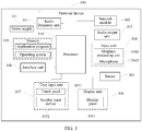
- FIG. 3 is a schematic diagram of a hardware structure of a terminal device implementing the various embodiments of the present disclosure.
- the terminal device 300 includes, but not limited to: a radio frequency unit 301, a network module 302, an audio output unit 303, an input unit 304, a sensor 305, a display unit 306, a user input unit 307, an interface unit 308, a memory 309, a processor 310, a power supply 311, and the like.
- the structure of the terminal device shown in FIG. 3 does not constitute a limitation to the terminal device.
- the terminal device may include more or fewer components than that shown in the figure, or a combination of some components, or an arrangement of different components.
- the terminal device includes but is not limited to a mobile phone, a tablet computer, a notebook computer, a palmtop computer, a vehicle-mounted terminal, a wearable device, a pedometer, or the like.
- the radio frequency unit 301 may be configured to receive and send signals in a process of receiving and sending information or calling. Specifically, the radio frequency unit 301 receives downlink data from a base station for processing by the processor 310, and sends uplink data to the base station. Generally, the radio frequency unit 301 includes, but is not limited to, an antenna, at least one amplifier, a transceiver, a coupler, a low noise amplifier, a duplexer, and the like. In addition, the radio frequency unit 301 may further communicate with other devices through a wireless communications system and network.
- the radio frequency unit 301 includes: a first communication module and a second communication module; a first switch connected to a first terminal of the first communication module and a first terminal of the second communication module; a second switch connected to a second terminal of the first communication module, and a first antenna structure connected to the second switch; and a third switch connected to a second terminal of the second communication module, and a second antenna structure connected to the third switch.
- the first communication module corresponds to a first transmitting link and two receiving links
- the second communication module corresponds to a second transmitting link and two receiving links; in a case of signal transmission, at least one of the first transmitting link and the second transmitting link is in a conductive state, and in a case of signal reception, the two receiving links corresponding to the first communication module and the two receiving links corresponding to the second communication module are all in a conductive state.
- the first switch, the second switch, and the third switch are all double-pole-double-throw switches.
- the radio frequency module 301 further includes: a modem.
- a first terminal of the first switch is connected to a first port and a second port of the modem, and a second terminal of the first switch is connected to a first transmitting port of the first communication module and a second transmitting port of the second communication module.
- a first terminal of the second switch is connected to a first transmitting/receiving port and a first signal reception port of the first communication module, and a second terminal of the second switch is connected to a first antenna and a second antenna of the first antenna structure.
- a first terminal of the third switch is connected to a second transmitting/receiving port and a second signal reception port of the second communication module, and a second terminal of the third switch is connected to a third antenna and a fourth antenna of the second antenna structure.
- the first communication module further includes: a first power amplifier, a first transmitting/receiving filter, a first receiving filter, a first transmission port, a second transmission port, and a first single-pole-double-throw switch.
- the first power amplifier is connected to the first transmitting port
- the first transmitting/receiving filter is connected to the first transmitting/receiving port
- a first non-movable terminal of the first single-pole-double-throw switch is connected to the first power amplifier
- a second non-movable terminal of the first single-pole-double-throw switch is connected to the first transmission port
- a movable terminal of the first single-pole-double-throw switch is connected to the first transmitting/receiving filter
- the second transmission port is connected to the first signal reception port through the first receiving filter
- the first transmission port and the second transmission port are both connected to a receiving port of the modem.
- the movable terminal and the first non-movable terminal of the first single-pole-double-throw switch are connected, the modem, the first switch, the first transmitting port, the first power amplifier, the first single-pole-double-throw switch, the first transmitting/receiving filter, the first transmitting/receiving port, the second switch, and a first transmitting antenna are connected in sequence, and the first transmitting antenna is the first antenna or the second antenna.
- the first communication module corresponds to the first receiving link and the second receiving link.
- the movable terminal and the second non-movable terminal of the first single-pole-double-throw switch are connected, and the first receiving antenna, the second switch, the first transmitting/receiving port, the first transmitting/receiving filter, the first single-pole-double-throw switch, the first transmission port, and the modem are connected in sequence;
- the second receiving antenna, the second switch, the first signal reception port, the first receiving filter, the second transmission port, and the modem are connected in sequence; and each of the first receiving antenna and the second receiving antenna is one of the first antenna and the second antenna.
- the second communication module further includes: a second power amplifier, a second transmitting/receiving filter, a second receiving filter, a third transmission port, a fourth transmission port, and a second single-pole-double-throw switch; where the second power amplifier is connected to the second transmitting port, the second transmitting/receiving filter is connected to the second transmitting/receiving port, a first non-movable terminal of the second single-pole-double-throw switch is connected to the second power amplifier, a second non-movable terminal of the second single-pole-double-throw switch is connected to the third transmission port, a movable terminal of the second single-pole-double-throw switch is connected to the second transmitting/receiving filter, the fourth transmission port is connected to the second signal reception port through the second receiving filter, and the third transmission port and the fourth transmission port are both connected to a receiving port of the modem.
- the movable terminal and the first non-movable terminal of the second single-pole-double-throw switch are connected, the modem, the first switch, the second transmitting port, the second power amplifier, the second single-pole-double-throw switch, the second transmitting/receiving filter, the second transmitting/receiving port, the third switch, and a second transmitting antenna are connected in sequence, and the second transmitting antenna is the third antenna or the fourth antenna.
- the second communication module corresponds to the third receiving link and the fourth receiving link.
- the third receiving link corresponding to the second communication module is conducted, the movable terminal and the second non-movable terminal of the second single-pole-double-throw switch are connected, and the third receiving antenna, the third switch, the second transmitting/receiving port, the second transmitting/receiving filter, the second single-pole-double-throw switch, the third transmission port, and the modem are connected in sequence;
- the fourth receiving antenna, the third switch, the second signal reception port, the second receiving filter, the fourth transmission port, and the modem are connected in sequence; and each of the third receiving antenna and the fourth receiving antenna is one of the third antenna and the fourth antenna.
- the first communication module and the second communication module are both 5G communication modules.
- the processor 310 is connected to the first switch, the second switch, the third switch, the first communication module, and the second communication module.
- the terminal device provides a user with wireless broadband Internet access through the network module 302, for example, helps the user send and receive emails, browse web pages, and access streaming media.
- the audio output unit 303 can convert audio data received by the radio frequency unit 301 or the network module 302 or stored in the memory 309 into an audio signal, and output the audio signal as sound.
- the audio output unit 303 may further provide audio output (for example, call signal receiving sound or message receiving sound) related to a specific function performed by the terminal device 300.
- the audio output unit 303 includes a speaker, a buzzer, a telephone receiver, and the like.
- the input unit 304 is configured to receive audio or video signals.
- the input unit 304 may include a graphics processing unit (Graphics Processing Unit, GPU) 3041 and a microphone 3042.
- the graphics processing unit 3041 processes image data of a static image or a video obtained by an image capturing apparatus (for example, a camera) in a video capturing mode or an image capturing mode.
- a processed image frame may be displayed on the display unit 306.
- the image frame processed by the graphics processing unit 3041 may be stored in the memory 309 (or another storage medium) or sent through the radio frequency unit 301 or the network module 302.
- the microphone 3042 may receive a sound and can process such sound into audio data. Processed audio data may be converted, in telephone call mode, into a format that may be sent to a mobile communication base station via the radio frequency unit 301 for output.
- the terminal device 300 further includes at least one sensor 305, such as an optical sensor, a motion sensor, and other sensors.
- the optical sensor includes an ambient optical sensor and a proximity sensor.
- the ambient optical sensor may adjust luminance of the display panel 3061 based on brightness of ambient light.
- the proximity sensor may turn off the display panel 3061 and/or backlight when the terminal device 300 approaches an ear.
- an accelerometer sensor may detect an acceleration in each direction (generally, three axes), and detect a value and a direction of gravity when the accelerometer sensor is static, and may be used to recognize a terminal device posture (such as screen switching between landscape and portrait modes, a related game, or magnetometer posture calibration), a function related to vibration recognition (such as a pedometer or a knock), and the like.
- the sensor 305 may further include a fingerprint sensor, a pressure sensor, an iris sensor, a molecular sensor, a gyroscope, a barometer, a hygrometer, a thermometer, and an infrared sensor. Details are not described herein.
- the display unit 306 is configured to display information input by a user or information provided to a user.
- the display unit 306 may include a display panel 3061, and the display panel 3061 may be configured in a form of liquid crystal display (Liquid Crystal Display, LCD), organic light-emitting diode (Organic Light-Emitting Diode, OLED), or the like.
- LCD Liquid Crystal Display
- OLED Organic Light-Emitting Diode
- the user input unit 307 may be configured to receive input numeral or character information, and generate key signal input related to user setting and function control of the terminal device.
- the user input unit 307 includes a touch panel 3071 and another input device 3072.
- the touch panel 3071 is also referred to as a touchscreen, and may collect a touch operation performed by a user on or near the touch panel 3071 (such as an operation performed by a user on the touch panel 3071 or near the touch panel 3071 by using any proper object or accessory, such as a finger or a stylus).
- the touch panel 3071 may include two parts: a touch detection apparatus and a touch controller.
- the touch detection apparatus detects a touch position of the user, detects a signal brought by the touch operation, and transmits the signal to the touch controller.
- the touch controller receives touch information from the touch detection apparatus, converts the touch information into contact coordinates, transmits the contact coordinates to the processor 310, receives a command sent by the processor 310, and executes the command.
- the touch panel 3071 may be implemented in various types such as resistive, capacitive, infrared, and surface acoustic wave.
- the user input unit 307 may also include the another input device 3072.
- the another input device 3072 may include, but not limited to, a physical keyboard, a function key (for example, a volume control key or a switch key), a trackball, a mouse, and a joystick. Details are not described herein.
- the touch panel 3071 may cover the display panel 3061. In the case of detecting a touch operation on or near the touch panel 3071, the touch panel 3071 transmits the touch operation to the processor 310 to determine a type of a touch event. Then the processor 310 provides corresponding visual output on the display panel 3061 based on the type of the touch event.
- the touch panel 3071 and the display panel 3061 are configured as two independent components to implement input and output functions of the terminal device, in some embodiments, the touch panel 3071 and the display panel 3061 may be integrated to implement the input and output functions of the terminal device. Details are not limited herein.
- the interface unit 308 is an interface for connecting an external apparatus to the terminal device 300.
- the external apparatus may include a wired or wireless headset jack, an external power supply (or a battery charger) port, a wired or wireless data port, a storage card port, a port for connecting an apparatus having an identification module, an audio input/output (I/O) port, a video I/O port, a headset jack, or the like.
- the interface unit 308 may be configured to receive an input (for example, data information or power) from an external apparatus and transmit the received input to one or more elements in the terminal device 300, or transmit data between the terminal device 300 and the external apparatus.
- the memory 309 may be configured to store a software program and various data.
- the memory 309 may mainly include a program storage area and a data storage area.
- the program storage area may store an operating system, an application program required by at least one function (such as a sound playback function and an image playback function), and the like.
- the data storage area may store data (such as audio data and an address book) created based on the use of the mobile phone, and the like.
- the memory 309 may include a high-speed random access memory or a nonvolatile memory, for example, at least one disk storage device, a flash memory, or another volatile solid-state storage device.
- the processor 310 is a control center of the terminal device, connects various parts of the entire terminal device by using various interfaces and circuits, and performs various functions of the terminal device and processes data by running or executing the software programs and/or the modules stored in the memory 309 and invoking data stored in the memory 309, so as to monitor the terminal device as a whole.
- the processor 310 may include one or more processing units.
- the processor 310 may be integrated with an application processor and a modem processor.
- the application processor mainly processes an operating system, a user interface, an application program, and the like, and the modem processor mainly processes wireless communication. It may be understood that alternatively, the modem processor may not be integrated into the processor 310.
- the terminal device 300 may further include the power supply 311 (such as a battery) that supplies power to each component.
- the power supply 311 may be logically connected to the processor 310 by using a power management system, to implement functions such as charging, discharging, and power consumption management by using the power management system.
- the terminal device 300 includes some functional modules that are not shown. Details are not described herein.
- the computer software product is stored in a storage medium (such as a read-only memory (Read-only Memory, ROM)/random access memory (Random Access Memory, RAM), a magnetic disk, or an optical disc) and includes several instructions for instructing user equipment (which may be a mobile phone, a computer, a server, an air conditioner, or a network device) to execute the methods described in the embodiments of the present disclosure.
- a storage medium such as a read-only memory (Read-only Memory, ROM)/random access memory (Random Access Memory, RAM), a magnetic disk, or an optical disc
- user equipment which may be a mobile phone, a computer, a server, an air conditioner, or a network device
Landscapes
- Engineering & Computer Science (AREA)
- Computer Networks & Wireless Communication (AREA)
- Signal Processing (AREA)
- Transceivers (AREA)
Abstract
Description
- This application claims priority to
Chinese Patent Application No.201910067093.2 filed in China on January 24, 2019 - The present disclosure relates to the field of communication technologies, and in particular, to a signal transceiving apparatus and a terminal device.
- With the development of economy and technologies and the continuous advancement of science and technologies, users have more and more requirements for mobile communication technologies. For example, users require for high reliability and a low latency to meet applications requirements of Internet of Vehicles, autonomous driving, telemedicine, and the like; users require for a higher communication rate to support an application requirement of ultra-high-definition videos; users require for low power consumption, large-connection scenarios, high traffic density, and the like to meet the requirements for widespread coverage of the Internet of Things and hotspot communication in smart industry and agriculture, and the like. To meet these requirements, the fifth-generation (5G for short) mobile communication technology appears. 5G introduces a new broadband spectrum, for example, a millimeter wave band and a band below 6G (sub 6G for short) meet broadband high-speed and low-latency coverage requirements, where sub 6G is divided into bands of 3.5 GHz (3.3 GHz to 4.2 GHz) and 4.5 GHz (4.4 GHz to 5.0 GHz). At the same time, a large-scale antenna technology, multiple access, beamforming, high-power terminal, and other technologies are further used to meet the above needs. At present, the 5G spectrum is planned as follows:
Band number Uplink frequency (MHZ) Downlink frequency (MHZ) Duplex mode n1 1920-1980 2110-2170 Frequency division duplex n2 1850-1910 1930-1990 Frequency division duplex n3 1710-1785 1805-1880 Frequency division duplex n5 824-849 869-894 Frequency division duplex n7 2500-2570 2620-2690 Frequency division duplex n8 880-915 925-960 Frequency division duplex n20 832-862 791-821 Frequency division duplex n28 703-748 758-803 Frequency division duplex n38 2570-2620 2570-2621 Time division duplex n41 2496-2690 2496-2691 Time division duplex n50 1432-1517 1432-1517 Time division duplex n51 1427-1432 1427-1432 Time division duplex n66 1710-1780 2110-2200 Frequency division duplex n70 1695-1710 1995-2020 Frequency division duplex n71 663-698 617-652 Frequency division duplex n74 1427-1470 1475-1518 Frequency division duplex n75 N/A 1432-1517 Supplementary downlink n76 N/A 1427-1432 Supplementary downlink n77 3300-4200 3300-4200 Time division duplex n78 3300-3800 3300-3800 Time division duplex n79 4400-5000 4400-5000 Time division duplex n80 1710-1785 N/A Supplementary uplink n81 880-915 N/A Supplementary uplink n82 832-862 N/A Supplementary uplink n83 703-748 N/A Supplementary uplink n84 1920-1980 N/A Supplementary uplink - It may be seen from the above list that the newly added sub 6G bands of 5G, that is, the n77, n78, and n79 bands all use time division duplexing (Time Division Duplexing, TDD) mode. Therefore, the proportion of TDD in 5G will increase, and more attention will be paid to the application of TDD. In addition, n1, n2, n3, n5, n7, n8, n38, n41, and other bands are all refarming (spectrum redeployment) bands of long term evolution (Long Term Evolution, LTE). Therefore, 4G and 5G will coexist for a long time. The terminal products tend to be lightweight and portable. The long-term coexistence of 4G and 5G will increase the printed circuit board (Printed Circuit Board, PCB) area and product weight of a terminal product. Therefore, decreasing the size and the weight of a terminal product is a major challenge at present. Because of the long-term coexistence of 4G and 5G, the large-scale access of 5G, and a high-power terminal technology, there are cases of transmitting by using one link and receiving by using four links (1T4R for short) and transmitting by using two links and receiving by using four links (2T4R for short). Therefore, the design of a radio frequency link becomes complicated. The realization of compatibility between multiple scenarios in a radio frequency architecture makes the design of a radio frequency link simple and convenient.
- At present, the compatible solution of 1T4R and 2T4R has a complex design architecture, use immature materials such as 3P3T (the larger the number of T, the worse the performance), and the wire is long, which affects the overall transmitting and receiving performance. Performance of 3P3T or 4P4T is worse than that of double-pole-double-throw (double-pole-double-throw, DPDT) switch, resulting in a large overall loss on a receiving channel. In addition, due to the price effect of new materials, the costs are much higher than those of the DPDT. In addition, in the current design solution, there is a port that is not used, which is very wasteful and occupies a larger PCB area. This increases the complexity of the design and the costs of the terminal product.
- The embodiments of the present disclosure provide a signal transceiving apparatus and a terminal device to solve the problem that a radio frequency transceiving system has a complex structure and a long wire, which affects transmitting and receiving performance, and causes high complexity of design and high costs of terminal products in the related technology.
- To resolve the foregoing problems, the embodiments of the present disclosure are implemented as follows:
- According to a first aspect, an embodiment of the present disclosure provides a signal transceiving apparatus, including:
- a first communication module and a second communication module;
- a first switch connected to a first terminal of the first communication module and a first terminal of the second communication module , respectively;
- a second switch connected to a second terminal of the first communication module, and a first antenna structure connected to the second switch; and
- a third switch connected to a second terminal of the second communication module, and a second antenna structure connected to the third switch; where
- the first communication module corresponds to a first transmitting link and two receiving links, the second communication module corresponds to a second transmitting link and two receiving links; in a case of signal transmission, at least one of the first transmitting link and the second transmitting link is in a conductive state, and in a case of signal reception, the two receiving links corresponding to the first communication module and the two receiving links corresponding to the second communication module are all in a conductive state.
- According to a second aspect, an embodiment of this disclosure provides a terminal device, including the signal transceiving apparatus.
- According to technical solutions of the present disclosure, the first terminal of the first communication module and the first terminal of the second communication module are respectively connected to the first switch, the second switch is disposed between the second terminal of the first communication module and the first antenna structure, and the third switch is disposed between the second terminal of the second communication module and the second antenna structure. By switching the states between on-switch and off-switch of the three switches, in a case of signal transmission, at least one of the first transmitting link corresponding to the first communication module and the second transmitting link corresponding to the second communication module is in a conductive state. In a case of signal reception, the two receiving links corresponding to the first communication module and the two receiving links corresponding to the second communication module are all in a conductive state. This can ensure the compatibility between the mode of transmitting by using one link and receiving by using four links and the mode of transmitting by using two links and receiving by using four links. In addition, the structural design can reduce insertion loss of the receiving link, improve performance of the transmitting link, shorten a wire length, and reduce the design complexity of the terminal device and reduce manufacturing costs.
- To describe the technical solutions of the embodiments of the present disclosure more clearly, the following briefly describes the accompanying drawings required for describing the embodiments of the present disclosure. Apparently, the accompanying drawings in the following description show merely some embodiments of the present disclosure, and a person of ordinary skill in the art may still derive other drawings from these accompanying drawings without creative efforts.
-
FIG. 1 is a schematic diagram of a signal transceiving apparatus according to an embodiment of this disclosure; -
FIG. 2 is a schematic diagram of cooperation between a signal transceiving apparatus and a processor according to an embodiment of this disclosure; and -
FIG. 3 is a schematic diagram of a hardware structure of a terminal device according to an embodiment of the present disclosure. - The following clearly and completely describes the technical solutions in the embodiments of the present disclosure with reference to the accompanying drawings in the embodiments of the present disclosure. Apparently, the described embodiments are some rather than all of the embodiments of the present disclosure. All other embodiments obtained by a person of ordinary skill in the art based on the embodiments of the present disclosure without creative efforts shall fall within the protection scope of the present disclosure. An embodiment of the present disclosure provides a signal transceiving apparatus. As shown in
FIG. 1 , the apparatus includes:
afirst communication module 11 and asecond communication module 12; afirst switch 2 connected to a first terminal of thefirst communication module 11 and a first terminal of thesecond communication module 12, respectively; asecond switch 31 connected to a second terminal of thefirst communication module 11, and a first antenna structure 4 connected to thesecond switch 31; and athird switch 32 connected to a second terminal of thesecond communication module 12, and asecond antenna structure 5 connected to thethird switch 32. - The
first communication module 11 corresponds to a first transmitting link and two receiving links, thesecond communication module 12 corresponds to a second transmitting link and two receiving links; in a case of signal transmission, at least one of the first transmitting link and the second transmitting link is in a conductive state, and in a case of signal reception, the two receiving links corresponding to thefirst communication module 11 and the two receiving links corresponding to thesecond communication module 12 are all in a conductive state. - The signal transceiving apparatus provided in the embodiments of the present disclosure includes: the
first communication module 11, thesecond communication module 12, thefirst switch 2, thesecond switch 31, thethird switch 32, the first antenna structure 4, and thesecond antenna structure 5. The first terminal of thefirst communication module 11 and the first terminal of thesecond communication module 12 are both connected to thefirst switch 2, the second terminal of thefirst communication module 11 is connected to the first antenna structure 4 through thesecond switch 31, and the second terminal of thesecond communication module 12 is connected to thesecond antenna structure 5 through thethird switch 32. - The
first communication module 11 corresponds to a first transmitting link and two receiving links, thesecond communication module 12 corresponds to a second transmitting link and two receiving links; in a case of signal transmission, the first transmitting link of thefirst communication module 11 and/or the second transmitting link of thesecond communication module 12 is conducted, and in a case of signal reception, the two receiving links of thefirst communication module 11 and the two receiving links of thesecond communication module 12 are all conducted. - In a case that the first transmitting link of the
first communication module 11 or the second transmitting link of thesecond communication module 12 is conducted, and the two receiving links of thefirst communication module 11 and the two receiving links of thesecond communication module 12 are all conducted, the mode of transmitting by using one link and receiving by using four links (1T4R) may be implemented. In a case that the first transmitting link of thefirst communication module 11 and the second transmitting link of thesecond communication module 12 are conducted, and the two receiving links of thefirst communication module 11 and the two receiving links of thesecond communication module 12 are all conducted, the mode of transmitting by using two links and receiving by using four links (2T4R) may be implemented. - The signal transceiving apparatus of the present disclosure can ensure the compatibility between two modes of transmitting by using one link and receiving by using four links and transmitting by using two links and receiving by using four links. In addition, the structural design can reduce insertion loss of the receiving link, improve performance of the transmitting link, shorten a wire length, and reduce the design complexity of the terminal device and reduce manufacturing costs.
- In the embodiments of the present disclosure, as shown in
FIG. 1 , thefirst switch 2, thesecond switch 31, and thethird switch 32 are all double-pole-double-throw switches. The signal transceiving apparatus further includes: amodem 6. A first terminal of thefirst switch 2 is connected to a first port and a second port of themodem 6, and a second terminal of thefirst switch 2 is connected to afirst transmitting port 111 of thefirst communication module 11 and asecond transmitting port 121 of thesecond communication module 12. - The
first switch 2 is a double-pole-double-throw switch, thefirst switch 2 may be connected to thefirst communication module 11 and thesecond communication module 12, and the first terminal of thefirst switch 2 is connected to themodem 6, and specifically connected to the first port and the second port of themodem 6. Herein, the first port and the second port are both transmitting ports. Thefirst communication module 11 includes the first transmittingport 111, thesecond communication module 12 includes the second transmittingport 121. The first transmittingport 111 is located at the first terminal of thefirst communication module 11, the second transmittingport 121 is located at the first terminal of thesecond communication module 12. The second terminal of thefirst switch 2 is connected to the first transmittingport 111 of thefirst communication module 11 and the second transmittingport 121 of thesecond communication module 12. - The first transmitting
port 111 may be connected to the first non-movable terminal of thefirst switch 2, the second transmittingport 121 is connected to the second non-movable terminal of thefirst switch 2, the first movable terminal of thefirst switch 2 is connected to the first port of themodem 6, and the second movable terminal of thefirst switch 2 is connected to the second port of themodem 6. The first movable terminal of thefirst switch 2 may be connected to the first non-movable terminal, and the second movable terminal may be connected to the second non-movable terminal, so that the first transmittingport 111 is connected to the first port of themodem 6, and the second transmittingport 121 is connected to the second port of themodem 6. The first movable terminal of thefirst switch 2 may be connected to the second non-movable terminal, and the second movable terminal may be connected to the first non-movable terminal, so that the first transmittingport 111 is connected to the second port of themodem 6, and the second transmittingport 121 is connected to the first port of themodem 6. - The
modem 6 may be connected to a baseband processor. In a case of signal transmission, themodem 6 converts a baseband signal transmitted by the baseband processor into a radio frequency signal, and sends the radio frequency signal through the first transmitting link and/or the second transmitting link; and in a case of signal reception, converts a received radio frequency signal into a baseband signal and transmits the baseband signal to the baseband processor, to implement processing of signal transmission and signal reception. - In the embodiments of the present disclosure, as shown in
FIG. 1 , a first terminal of thesecond switch 31 is connected to a first transmitting/receivingport 112 and a firstsignal reception port 113 of thefirst communication module 11, and a second terminal of thesecond switch 31 is connected to afirst antenna 41 and asecond antenna 42 of the first antenna structure 4. - The
first communication module 11 includes the first transmitting/receivingport 112 and the firstsignal reception port 113 located at the second terminal, the first antenna structure 4 includes thefirst antenna 41 and thesecond antenna 42, and thesecond switch 31 is disposed between thefirst communication module 11 and the first antenna structure 4. In addition, because thesecond switch 31 is a double-pole-double-throw switch, a first terminal of thesecond switch 31 may be connected to a first transmitting/receivingport 112 and a firstsignal reception port 113, and a second terminal of thesecond switch 31 is connected to afirst antenna 41 and asecond antenna 42. - The first transmitting/receiving
port 112 is connected to the first movable terminal of thesecond switch 31, the firstsignal reception port 113 is connected to the second movable terminal of thesecond switch 31, and the first non-movable terminal and the second non-movable terminal of thesecond switch 31 are connected to thefirst antenna 41 and thesecond antenna 42 of the first antenna structure 4. The first movable terminal of thesecond switch 31 may be connected to the first non-movable terminal, and the second movable terminal of thesecond switch 31 may be connected to the second non-movable terminal, so that the first transmitting/receivingport 112 is connected to thefirst antenna 41, and the firstsignal reception port 113 is connected to thesecond antenna 42. The first movable terminal of thesecond switch 31 further may be connected to the second non-movable terminal, and the second movable terminal may be connected to the first non-movable terminal, so that the first transmitting/receivingport 112 is connected to thesecond antenna 42, and the firstsignal reception port 113 is connected to thefirst antenna 41. - That is, the first transmitting/receiving
port 112 may be connected to thefirst antenna 41, and the firstsignal reception port 113 may be connected to thesecond antenna 42 by thesecond switch 31, or the first transmitting/receivingport 112 may be connected to thesecond antenna 42, and the firstsignal reception port 113 may be connected to thefirst antenna 41 by thesecond switch 31. - In the embodiments of the present disclosure, a first terminal of the
third switch 32 is connected to 12 a second transmitting/receivingport 122 and a secondsignal reception port 123 of the second communication module, and a second terminal of thethird switch 32 is connected to athird antenna 51 and afourth antenna 52 of thesecond antenna structure 5. - The
second communication module 12 includes the second transmitting/receivingport 122 and the secondsignal reception port 123 located at the second terminal, thesecond antenna structure 5 includes thethird antenna 51 and thefourth antenna 52, and thethird switch 32 is disposed between thesecond communication module 12 and thesecond antenna structure 5. In addition, because thethird switch 32 is a double-pole-double-throw switch, a first terminal of thethird switch 32 may be connected to a second transmitting/receivingport 122 and a secondsignal reception port 123, and a second terminal of thethird switch 32 is connected to athird antenna 51 and afourth antenna 52. - The second transmitting/receiving
port 122 is connected to the first movable terminal of thethird switch 32, the secondsignal reception port 123 is connected to the second movable terminal of thethird switch 32, and the first non-movable terminal and the second non-movable terminal of thethird switch 32 are connected to thethird antenna 51 and thefourth antenna 52 of thesecond antenna structure 5. The first movable terminal of thethird switch 32 may be connected to the first non-movable terminal, and the second movable terminal of thethird switch 32 may be connected to the second non-movable terminal, so that the second transmitting/receivingport 122 is connected to thethird antenna 51, and the secondsignal reception port 123 is connected to thefourth antenna 52. The first movable terminal of thethird switch 32 further may be connected to the second non-movable terminal, and the second movable terminal may be connected to the first non-movable terminal, so that the second transmitting/receivingport 122 is connected to thefourth antenna 52, and the secondsignal reception port 123 is connected to thethird antenna 51. - That is, the second transmitting/receiving
port 122 is connected to thethird antenna 51, and the secondsignal reception port 123 is connected to thefourth antenna 52 by thethird switch 32, or the second transmitting/receivingport 122 is connected to thefourth antenna 52, and the secondsignal reception port 123 is connected to thethird antenna 51 by thethird switch 32. - The mature double-pole-double-throw switch with advantages in both insertion loss and isolation is used to replace the 3P3T disposed between the communication module and the antenna structure, which can reduce insertion loss of a receiving path and reduce costs. At the same time, the double-pole-double-throw switch is added before the transmitting link (between the communication module and the modem), which can eliminate the insertion loss and load impact, improve the transmitting performance, and shorten the wire length. In addition, this can achieve compatibility between two modes of transmitting by using one link and receiving by using four links and transmitting by using two links and receiving by using four links, and reduce the complexity of design of a radio frequency link.
- In the embodiments of the present disclosure, as shown in
FIG. 1 , thefirst communication module 11 further includes: thefirst power amplifier 114, the first transmitting/receivingfilter 115, the first receivingfilter 116, thefirst transmission port 117, thesecond transmission port 118, and the first single-pole-double-throw switch 119. Thefirst power amplifier 114 is connected to the first transmittingport 111, the first transmitting/receivingfilter 115 is connected to the first transmitting/receivingport 112, a first non-movable terminal of the first single-pole-double-throw switch 119 is connected to thefirst power amplifier 114, a second non-movable terminal of the first single-pole-double-throw switch 119 is connected to thefirst transmission port 117, a movable terminal of the first single-pole-double-throw switch 119 is connected to the first transmitting/receivingfilter 115, thesecond transmission port 118 is connected to the firstsignal reception port 113 through the first receivingfilter 116, and thefirst transmission port 117 and thesecond transmission port 118 are both connected to a receiving port of themodem 6. - In addition to the first transmitting
port 111, the first transmitting/receivingport 112, and the firstsignal reception port 113, thefirst communication module 11 further includes: afirst power amplifier 114 for power amplification connected to the first transmittingport 111, a first transmitting/receivingfilter 115 for transmitting and receiving multiplexing connected to the first transmitting/receivingport 112, afirst transmission port 117 and asecond transmission port 118 located at the same terminal as that of the first transmittingport 111, a first receivingfilter 116 disposed between thesecond transmission port 118 and the firstsignal reception port 113 and connected to thesecond transmission port 118 and the firstsignal reception port 113, and a first single-pole-double-throw switch 119 for switching between transmitting and receiving links. Two non-movable terminals of the first single-pole-double-throw switch 119 are connected to thefirst power amplifier 114 and thefirst transmission port 117, and the movable terminal of the first single-pole-double-throw switch 119 is connected to the first transmitting/receivingfilter 115. Through switch switching of the first single-pole-double-throw switch 119, the first transmitting/receivingfilter 115 may be connected to thefirst power amplifier 114, or the first transmitting/receivingfilter 115 may be connected to thefirst transmission port 117. Thefirst transmission port 117 and thesecond transmission port 118 are receiving ports, and are both connected to the receiving port of themodem 6 to transmit a received radio frequency signal to themodem 6. - In a case that the first transmitting link corresponding to the
first communication module 11 is conducted, the movable terminal and the first non-movable terminal of the first single-pole-double-throw switch 119 are connected. At this time, the first single-pole-double-throw switch 119 connects thefirst power amplifier 114 to the first transmitting/receivingfilter 115. Themodem 6, thefirst switch 2, the first transmittingport 111, thefirst power amplifier 114, the first single-pole-double-throw switch 119, the first transmitting/receivingfilter 115, the first transmitting/receivingport 112, thesecond switch 31, and a first transmitting antenna are connected in sequence, and the first transmitting antenna is thefirst antenna 41 or thesecond antenna 42. - In a case that the first single-pole-double-
throw switch 119 connects thefirst power amplifier 114 to the first transmitting/receivingfilter 115, themodem 6, thefirst switch 2, the first transmittingport 111, thefirst power amplifier 114, the first single-pole-double-throw switch 119, the first transmitting/receivingfilter 115, the first transmitting/receivingport 112, thesecond switch 31, and a first transmitting antenna are connected, so that the first transmitting link may be formed. - The
first communication module 11 corresponds to the first receiving link and the second receiving link. In a case that the first receiving link corresponding to thefirst communication module 11 is conducted, the movable terminal of the first single-pole-double-throw switch 119 is connected to the second non-movable terminal, a first receiving antenna, thesecond switch 31, the first transmitting/receivingport 112, the first transmitting/receivingfilter 115, the first single-pole-double-throw switch 119, thefirst transmission port 117, and themodem 6 are connected in sequence. In a case that the second receiving link corresponding to thefirst communication module 11 is conducted, a second receiving antenna, thesecond switch 31, the firstsignal reception port 113, the first receivingfilter 116, thesecond transmission port 118, and themodem 6 are connected in sequence. Each of the first receiving antenna and the second receiving antenna is one of thefirst antenna 41, thesecond antenna 42. - In a case that the first single-pole-double-
throw switch 119 connects thefirst transmission port 117 to the first transmitting/receivingfilter 115, the first receiving antenna, thesecond switch 31, the first transmitting/receivingport 112, the first transmitting/receivingfilter 115, the first single-pole-double-throw switch 119, thefirst transmission port 117, and themodem 6 are connected, so that the first receiving link may be formed. The second receiving antenna, thesecond switch 31, the firstsignal reception port 113, the first receivingfilter 116, thesecond transmission port 118, and themodem 6 are connected in sequence; and are always in a conductive state, so that the second receiving link may be formed. In a case that the first receiving link is conducted, thefirst power amplifier 114 may be in an off state. - Each of the first receiving antenna and the second receiving antenna is one of the
first antenna 41 and thesecond antenna 42, that is, in a case that the first receiving antenna is thefirst antenna 41, the second receiving antenna is thesecond antenna 42. Correspondingly, in a case that the first receiving antenna is thesecond antenna 42, the second receiving antenna is thefirst antenna 41. - In the embodiments of the present disclosure, as shown in
FIG. 1 , thesecond communication module 12 further includes: asecond power amplifier 124, a second transmitting/receivingfilter 125, asecond receiving filter 126, athird transmission port 127, afourth transmission port 128, and a second single-pole-double-throw switch 129; where
thesecond power amplifier 124 is connected to the second transmittingport 121, the second transmitting/receivingfilter 125 is connected to the second transmitting/receivingport 122, a first non-movable terminal of the second single-pole-double-throw switch 129 is connected to thesecond power amplifier 124, a second non-movable terminal of the second single-pole-double-throw switch 129 is connected to thethird transmission port 127, a movable terminal of the second single-pole-double-throw switch 129 is connected to the second transmitting/receivingfilter 125, thefourth transmission port 128 is connected to the secondsignal reception port 123 through the second receivingfilter 126, and thethird transmission port 127 and thefourth transmission port 128 are both connected to a receiving port of themodem 6. - In addition to the second transmitting
port 121, the second transmitting/receivingport 122, and the secondsignal reception port 123, thesecond communication module 12 further includes: asecond power amplifier 124 for power amplification connected to the second transmittingport 121, a second transmitting/receivingfilter 125 for transmitting and receiving multiplexing connected to the second transmitting/receivingport 122, athird transmission port 127 and afourth transmission port 128 located at the same terminal as the second transmittingport 121, asecond receiving filter 126 disposed between thefourth transmission port 128 and the secondsignal reception port 123 and connected to thefourth transmission port 128 and the secondsignal reception port 123, and a second single-pole-double-throw switch 129 for switching a transmitting and receiving link. Two non-movable terminals of the second single-pole-double-throw switch 129 are connected to thesecond power amplifier 124 and thethird transmission port 127, and the movable terminal of the second single-pole-double-throw switch 129 is connected to the second transmitting/receivingfilter 125. Through state switching of the second single-pole-double-throw switch 129, the second transmitting/receivingfilter 125 may be connected to thesecond power amplifier 124, or the second transmitting/receivingfilter 125 may be connected to thethird transmission port 127. Thethird transmission port 127 and thefourth transmission port 128 are receiving ports, and are both connected to the receiving port of themodem 6, to transmit a received radio frequency signal to themodem 6. - In a case that the second transmitting link corresponding to the
second communication module 12 is conducted, the movable terminal and the first non-movable terminal of the second single-pole-double-throw switch 129 are connected, themodem 6, thefirst switch 2, the second transmittingport 121, thesecond power amplifier 124, the second single-pole-double-throw switch 129, the second transmitting/receivingfilter 125, the second transmitting/receivingport 122, thethird switch 32, and a second transmitting antenna are connected in sequence, and the second transmitting antenna is thethird antenna 51 or thefourth antenna 52. - In a case that the second single-pole-double-
throw switch 129 connects thesecond power amplifier 124 to the second transmitting/receivingfilter 125, themodem 6, thefirst switch 2, the second transmittingport 121, thesecond power amplifier 124, the second single-pole-double-throw switch 129, the second transmitting/receivingfilter 125, the second transmitting/receivingport 122, thethird switch 32, and a second transmitting antenna are connected, so that the second transmitting link may be formed. - The
second communication module 12 corresponds to the third receiving link and the fourth receiving link. In a case that the third receiving link corresponding to thesecond communication module 12 is conducted, the movable terminal of the second single-pole-double-throw switch 129 is connected to the second non-movable terminal, a third receiving antenna, thethird switch 32, the second transmitting/receivingport 122, the second transmitting/receivingfilter 125, the second single-pole-double-throw switch 129, thethird transmission port 127, and themodem 6 are connected in sequence. In a case that the fourth receiving link corresponding to thesecond communication module 12 is conducted, a fourth receiving antenna, thethird switch 32, the secondsignal reception port 123, the second receivingfilter 126, thefourth transmission port 128, and themodem 6 are connected in sequence. Each of the third receiving antenna and the fourth receiving antenna is one of thethird antenna 51 and thefourth antenna 52. - In a case that the second single-pole-double-
throw switch 129 connects thethird transmission port 127 to the second transmitting/receivingfilter 125, the third receiving antenna, thethird switch 32, the second transmitting/receivingport 122, the second transmitting/receivingfilter 125, the second single-pole-double-throw switch 129, thethird transmission port 127, and themodem 6 are connected, so that the third receiving link may be formed. The fourth receiving antenna, thethird switch 32, the secondsignal reception port 123, the second receivingfilter 126, thefourth transmission port 128, and themodem 6 are connected in sequence; and are always in a conductive state, so that the fourth receiving link may be formed. In a case that the third receiving link is conducted, thesecond power amplifier 124 may be in an off state. - In a case that the third receiving antenna is the
third antenna 51, the fourth receiving antenna is thefourth antenna 52. Correspondingly, in a case that the third receiving antenna is thefourth antenna 52, the fourth receiving antenna is thethird antenna 51. - In the foregoing embodiments of the present disclosure, the
first communication module 11 and thesecond communication module 12 are both 5G communication modules, which may realize compatibility of two modes of transmitting by using one link and receiving by using four links and transmitting by using two links and receiving by using four links in 4G and 5G coexistence mode and 5G large-scale access. This reduces the design complexity of the terminal device, improves performance, and reduces manufacturing costs. - Optionally, the
first communication module 11 and thesecond communication module 12 may be communication circuits or communication chips. - In the signal transceiving apparatus provided in the embodiments of the present disclosure, the first terminal of the first communication module and the first terminal of the second communication module are respectively connected to the first switch, the second switch is disposed between the second terminal of the first communication module and the first antenna structure, and the third switch is disposed between the second terminal of the second communication module and the second antenna structure. By setting connection states of the three switches, in a case of signal transmission, at least one of the first transmitting link corresponding to the first communication module and the second transmitting link corresponding to the second communication module is in a conductive state. In a case of signal reception, the two receiving links corresponding to the first communication module and the two receiving links corresponding to the second communication module are all in a conductive state. This can ensure the compatibility between modes of transmitting by using one link and receiving by using four links and transmitting by using two links and receiving by using four links. In addition, the structural design can reduce insertion loss of the receiving link, improve performance of the transmitting link, shorten a wire length, and reduce the design complexity of the terminal device and reduce manufacturing costs.
- An embodiment of this disclosure further provides a terminal device, including the signal transceiving apparatus. As shown in
FIG. 2 , the terminal device further includes aprocessor 7, which is connected to the signal transceiving apparatus, and may control the operation of the signal transceiving apparatus. - The
processor 7 is specifically connected to thefirst switch 2, thesecond switch 31, thethird switch 32, thefirst communication module 11, and thesecond communication module 12 of the signal transceiving apparatus. In the mode of transmitting by using two links and receiving by using four links, theprocessor 7 may determine the first transmitting antenna in thefirst antenna 41 and thesecond antenna 42, and determine the second transmitting antenna in thethird antenna 51 and thefourth antenna 52 according to an environmental reference signal. In the mode of transmitting by using one link and receiving by using four links, theprocessor 7 may determine the transmitting antenna in thefirst antenna 41, thesecond antenna 42, thethird antenna 51, and thefourth antenna 52 according to an environmental reference signal. - As shown in
FIG. 1 andFIG. 2 , in the mode of transmitting by using two links and receiving by using four links, theprocessor 7 is connected to the network to monitor the environmental reference signal in real time. For thefirst communication module 11, theprocessor 7 needs to determine an antenna with a better environmental reference signal in thefirst antenna 41 and thesecond antenna 42 as the first transmitting antenna. Then, theprocessor 7 sends a control signal to thesecond switch 31, so that the first transmitting/receivingport 112 of thefirst communication module 11 is connected to the first transmitting antenna through thesecond switch 31, and the firstsignal reception port 113 of thefirst communication module 11 is connected to another antenna through thesecond switch 31. - The
processor 7 may control thefirst switch 2 in advance to connect the first transmittingport 111 of thefirst communication module 11 to the first port or the second port of themodem 6. In a case of signal transmission, theprocessor 7 controls the first single-pole-double-throw switch 119 to connect thefirst power amplifier 114 to the first transmitting/receivingfilter 115. At this time, a transmitted signal enters the first transmittingport 111 from the first port or the second port of themodem 6 through thefirst switch 2, is transmitted by the first transmittingport 111 to thefirst power amplifier 114, is amplified in thefirst power amplifier 114, then is transmitted to the first transmitting/receivingfilter 115, is filtered in the first transmitting/receivingfilter 115, and is transmitted to the first transmitting antenna through the first transmitting/receivingport 112 and thesecond switch 31. The signal is sent by the first transmitting antenna. - When receiving a radio frequency signal, the
processor 7 can control thefirst power amplifier 114 to be in a turn-off state, and control the first single-pole-double-throw switch 119 to connect thefirst transmission port 117 to the first transmitting/receivingfilter 115. Based on an initial default configuration of thesecond switch 31, a channel of radio frequency signal received by the antenna is transmitted to the first transmitting/receivingfilter 115 through the first transmitting/receivingport 112, and then is transmitted to thefirst transmission port 117 after the filtering is completed. Based on an initial default configuration of thesecond switch 31, another channel of radio frequency signal received by the antenna is transmitted to the first receivingfilter 116 through the firstsignal reception port 113, and then is transmitted to thesecond transmission port 118 after filtering is completed. Thefirst transmission port 117 and thesecond transmission port 118 are connected to the receiving port of themodem 6, to realize signal transmission to themodem 6, and themodem 6 processes the received signal and then transmits the signal to the baseband processor. - It should be noted that a connection status of the first port and the second port of the
modem 6 and thefirst communication module 11 and thesecond communication module 12 may be autonomously set by a user. - For the
second communication module 12, theprocessor 7 needs to determine an antenna with a better environmental reference signal in thethird antenna 51 and thefourth antenna 52 as the second transmitting antenna. Then, theprocessor 7 sends a control signal to thethird switch 32, so that the second transmitting/receivingport 122 of thesecond communication module 12 is connected to the second transmitting antenna through thethird switch 32, and the secondsignal reception port 123 of thesecond communication module 12 is connected to another antenna through thethird switch 32. - The
processor 7 may control thefirst switch 2 in advance to connect the second transmittingport 121 of thesecond communication module 12 to the second port or the first port of themodem 6. In a case of signal transmission, theprocessor 7 controls the second single-pole-double-throw switch 129 to connect thesecond power amplifier 124 to the second transmitting/receivingfilter 125. At this time, a transmitted signal enters the second transmittingport 121 from the second port or the first port of themodem 6 through thefirst switch 2, is transmitted by the second transmittingport 121 to thesecond power amplifier 124, is amplified in thesecond power amplifier 124, then is transmitted to the second transmitting/receivingfilter 125, is filtered in the second transmitting/receivingfilter 125, and is transmitted to the second transmitting antenna through the second transmitting/receivingport 122 and thethird switch 32. The signal is sent by the second transmitting antenna. - In the case of receiving a radio frequency signal, the
processor 7 can control thesecond power amplifier 124 to be in a turn-off state, and control the second single-pole-double-throw switch 129 to connect thethird transmission port 127 to the second transmitting/receivingfilter 125. Based on an initial default configuration of thethird switch 32, a channel of radio frequency signal received by the antenna is transmitted to the second transmitting/receivingfilter 125 through the second transmitting/receivingport 122, and then is transmitted to thethird transmission port 127 after the filtering is completed. Based on an initial default configuration of thethird switch 32, another channel of radio frequency signal received by the antenna is transmitted to the second receivingfilter 126 through the secondsignal reception port 123, and then is transmitted to thefourth transmission port 128 after filtering is completed. Thethird transmission port 127 and thefourth transmission port 128 are connected to the receiving port of themodem 6, to transmit a signal to themodem 6. Themodem 6 processes the received signal and then transmits the signal to the baseband processor. - In the above process, the first transmitting antenna and the second transmitting antenna are determined by monitoring the environmental reference signal in real time, and the determined first transmitting antenna and second transmitting antenna are used for transmission, to achieve the mode of transmitting by using two links and receiving by using four links and improve communication quality.
- As shown in
FIG. 1 andFIG. 2 , in the mode of transmitting by using one link and receiving by using four links, theprocessor 7 is connected to the network to monitor the environmental reference signal in real time. An antenna with a better environmental reference signal is determined in thefirst antenna 41, thesecond antenna 42, thethird antenna 51, and thefourth antenna 52 as the transmitting antenna. In a case that the transmitting antenna is thefirst antenna 41 or thesecond antenna 42, theprocessor 7 may control thesecond communication module 12 to be in a turn-off state to save power, and can still control thethird switch 32 to connect the second transmitting/receivingport 122 of thesecond communication module 12 to thethird antenna 51 or thefourth antenna 52, and connect the secondsignal reception port 123 of thesecond communication module 12 to thefourth antenna 52 or thethird antenna 51. - The
processor 7 controls thefirst communication module 11 to be in an active state, and a control signal is sent to thesecond switch 31, so that the first transmitting/receivingport 112 of thefirst communication module 11 is connected to the transmitting antenna through thesecond switch 31, and the firstsignal reception port 113 of thefirst communication module 11 is connected to another antenna through thesecond switch 31. - The
processor 7 may control thefirst switch 2 in advance to connect the first transmittingport 111 of thefirst communication module 11 to the first port or the second port of themodem 6 and connect the second transmittingport 121 of thesecond communication module 12 to the second port or the first port of themodem 6. - In a case of signal transmission, the
processor 7 controls the first single-pole-double-throw switch 119 to connect thefirst power amplifier 114 to the first transmitting/receivingfilter 115. At this time, a transmitted signal enters the first transmittingport 111 from the first port or the second port of themodem 6 through thefirst switch 2, is transmitted by the first transmittingport 111 to thefirst power amplifier 114, is amplified in thefirst power amplifier 114, is transmitted to the first transmitting/receivingfilter 115, is filtered in the first transmitting/receivingfilter 115, and is transmitted to the transmitting antenna through the first transmitting/receivingport 112 and thesecond switch 31. The signal is sent by the transmitting antenna. - In the case of receiving a radio frequency signal, the
processor 7 can control thefirst power amplifier 114 to be in a turn-off state, control the first single-pole-double-throw switch 119 to connect thefirst transmission port 117 to the first transmitting/receivingfilter 115, control thesecond communication module 12 to turn on, and control the second single-pole-double-throw switch 129 to connect thethird transmission port 127 to the second transmitting/receivingfilter 125. At this time, theprocessor 7 can control thefirst power amplifier 114 and thesecond power amplifier 124 to be in a turn-off state. For thefirst antenna 41 or thesecond antenna 42, based on an initial default configuration of thesecond switch 31, a channel of radio frequency signal received by the antenna is transmitted to the first transmitting/receivingfilter 115 through the first transmitting/receivingport 112, and then is transmitted to thefirst transmission port 117 after the filtering is completed. Based on an initial default configuration of thesecond switch 31, another channel of radio frequency signal received by the antenna is transmitted to the first receivingfilter 116 through the firstsignal reception port 113, and then is transmitted to thesecond transmission port 118 after filtering is completed. For thethird antenna 51 or thefourth antenna 52, based on an initial default configuration of thethird switch 32, a channel of radio frequency signal received by the antenna is transmitted to the second transmitting/receivingfilter 125 through the second transmitting/receivingport 122, and then is transmitted to thethird transmission port 127 after the filtering is completed. Based on an initial default configuration of thethird switch 32, another channel of radio frequency signal received by the antenna is transmitted to the second receivingfilter 126 through the secondsignal reception port 123, and then is transmitted to thefourth transmission port 128 after filtering is completed. - The
first transmission port 117, thesecond transmission port 118, thethird transmission port 127, and thefourth transmission port 128 are connected to the receiving port of themodem 6, to realize signal transmission to themodem 6, and themodem 6 processes the received signal and then transmits the signal to the baseband processor. - In summary, in a transmitting phase, the processor may control the first transmitting link of the first communication module to achieve radio frequency signal transmission. In a receiving phase, the processor may control the first receiving link and the second receiving link of the first communication module to be conducted, control the second communication module to turn on, and control the third receiving link and the fourth receiving link of the second communication module to be conducted, to realize radio frequency signal reception.
- In a case that the transmitting antenna is the
third antenna 51 or thefourth antenna 52, theprocessor 7 may control thefirst communication module 11 to be in a turn-off state to save power, and can still control thesecond switch 31 to connect the first transmitting/receivingport 112 of thefirst communication module 11 to thefirst antenna 41 or thesecond antenna 42, and connect the firstsignal reception port 113 of thefirst communication module 11 to thesecond antenna 42 or thefirst antenna 41. - The
processor 7 controls thesecond communication module 12 to be in an active state, and a control signal is sent to thethird switch 32, so that the second transmitting/receivingport 122 of thesecond communication module 12 is connected to the transmitting antenna through thethird switch 32, and the secondsignal reception port 123 of thesecond communication module 12 is connected to another antenna through thethird switch 32. - The
processor 7 may control thefirst switch 2 in advance to connect the first transmittingport 111 of thefirst communication module 11 to the first port or the second port of themodem 6 and connect the second transmittingport 121 of thesecond communication module 12 to the second port or the first port of themodem 6. - In a case of signal transmission, the
processor 7 controls the second single-pole-double-throw switch 129 to connect thesecond power amplifier 124 to the second transmitting/receivingfilter 125. At this time, a transmitted signal enters the second transmittingport 121 from the first port or the second port of themodem 6 through thefirst switch 2, is transmitted by the second transmittingport 121 to thesecond power amplifier 124, is amplified in thesecond power amplifier 124, then is transmitted to the second transmitting/receivingfilter 125, is filtered in the second transmitting/receivingfilter 125, and is transmitted to the transmitting antenna through the second transmitting/receivingport 122 and thethird switch 32. The transmitting antenna performs signal transmission. - In the case of receiving a radio frequency signal, the
processor 7 can control thesecond power amplifier 124 to be in a turn-off state, control the second single-pole-double-throw switch 129 to connect thethird transmission port 127 to the second transmitting/receivingfilter 125, control thefirst communication module 11 to turn on, and control the first single-pole-double-throw switch 119 to connect thefirst transmission port 117 to the first transmitting/receivingfilter 115. At this time, theprocessor 7 can control thefirst power amplifier 114 and thesecond power amplifier 124 to be in a turn-off state. For thefirst antenna 41 or thesecond antenna 42, based on an initial default configuration of thesecond switch 31, a channel of radio frequency signal received by the antenna is transmitted to the first transmitting/receivingfilter 115 through the first transmitting/receivingport 112, and then is transmitted to thefirst transmission port 117 after the filtering is completed. Based on an initial default configuration of thesecond switch 31, another channel of radio frequency signal received by the antenna is transmitted to the first receivingfilter 116 through the firstsignal reception port 113, and then is transmitted to thesecond transmission port 118 after filtering is completed. For thethird antenna 51 or thefourth antenna 52, based on an initial default configuration of thethird switch 32, a channel of radio frequency signal received by the antenna is transmitted to the second transmitting/receivingfilter 125 through the second transmitting/receivingport 122, and then is transmitted to thethird transmission port 127 after the filtering is completed. Based on an initial default configuration of thethird switch 32, another channel of radio frequency signal received by the antenna is transmitted to the second receivingfilter 126 through the secondsignal reception port 123, and then is transmitted to thefourth transmission port 128 after filtering is completed. - In summary, in a transmitting phase, the processor may control the second transmitting link of the second communication module to achieve radio frequency signal transmission. In a receiving phase, the processor may control the third receiving link and the fourth receiving link of the second communication module to be conducted, control the first communication module to turn on, and control the first receiving link and the second receiving link of the first communication module to be conducted, to realize radio frequency signal reception.
- In the embodiments of the present disclosure, the first single-pole-double-
throw switch 119 and the second single-pole-double-throw switch 129 are connected to theprocessor 7, and may switch between states according to the control of theprocessor 7, and thefirst power amplifier 114 and thesecond power amplifier 124 are connected to theprocessor 7, and may switch between a working state and a non-working state according to the control of theprocessor 7. - Through the cooperation of the first switch, the second switch, and the third switch, the modes of transmitting by using one link and receiving by using four links and transmitting by using two links and receiving by using four links are compatible. At the same time, the transmitting antenna switches between the 4 antennas. Through the cooperation between the processor and the signal transceiving apparatus, an antenna with a better uplink may be selected according to the environmental reference signal, to ensure the communication quality of the signal transceiving apparatus and avoid the problem of poor communication quality in complex scenarios.
- In summary, the implementation process of modes of transmitting by using one link and receiving by using four links and transmitting by using two links and receiving by using four links is provided above. By disposing the first switch, the second switch, and the third switch, insertion loss of the receiving link may be reduced, performance of the transmitting link may be improved, and the wire length may be reduced. In addition, this can ensure the compatibility of modes of transmitting by using one link and receiving by using four links and transmitting by using two links and receiving by using four links, the selection of the uplink according to the environmental reference signal, and ensure the communication quality. Besides, the structural design may reduce the design complexity of the terminal device, improve the performance, and reduce manufacturing costs.
-
FIG. 3 is a schematic diagram of a hardware structure of a terminal device implementing the various embodiments of the present disclosure. Theterminal device 300 includes, but not limited to: aradio frequency unit 301, anetwork module 302, anaudio output unit 303, aninput unit 304, asensor 305, adisplay unit 306, auser input unit 307, aninterface unit 308, amemory 309, aprocessor 310, apower supply 311, and the like. - A person skilled in the art may understand that the structure of the terminal device shown in
FIG. 3 does not constitute a limitation to the terminal device. The terminal device may include more or fewer components than that shown in the figure, or a combination of some components, or an arrangement of different components. In this embodiment of the present disclosure, the terminal device includes but is not limited to a mobile phone, a tablet computer, a notebook computer, a palmtop computer, a vehicle-mounted terminal, a wearable device, a pedometer, or the like. - It should be understood that in this embodiment of this disclosure, the
radio frequency unit 301 may be configured to receive and send signals in a process of receiving and sending information or calling. Specifically, theradio frequency unit 301 receives downlink data from a base station for processing by theprocessor 310, and sends uplink data to the base station. Generally, theradio frequency unit 301 includes, but is not limited to, an antenna, at least one amplifier, a transceiver, a coupler, a low noise amplifier, a duplexer, and the like. In addition, theradio frequency unit 301 may further communicate with other devices through a wireless communications system and network. - The
radio frequency unit 301 includes: a first communication module and a second communication module; a first switch connected to a first terminal of the first communication module and a first terminal of the second communication module; a second switch connected to a second terminal of the first communication module, and a first antenna structure connected to the second switch; and a third switch connected to a second terminal of the second communication module, and a second antenna structure connected to the third switch. The first communication module corresponds to a first transmitting link and two receiving links, the second communication module corresponds to a second transmitting link and two receiving links; in a case of signal transmission, at least one of the first transmitting link and the second transmitting link is in a conductive state, and in a case of signal reception, the two receiving links corresponding to the first communication module and the two receiving links corresponding to the second communication module are all in a conductive state. - The first switch, the second switch, and the third switch are all double-pole-double-throw switches.
- The
radio frequency module 301 further includes: a modem. A first terminal of the first switch is connected to a first port and a second port of the modem, and a second terminal of the first switch is connected to a first transmitting port of the first communication module and a second transmitting port of the second communication module. - A first terminal of the second switch is connected to a first transmitting/receiving port and a first signal reception port of the first communication module, and a second terminal of the second switch is connected to a first antenna and a second antenna of the first antenna structure.
- A first terminal of the third switch is connected to a second transmitting/receiving port and a second signal reception port of the second communication module, and a second terminal of the third switch is connected to a third antenna and a fourth antenna of the second antenna structure.
- The first communication module further includes: a first power amplifier, a first transmitting/receiving filter, a first receiving filter, a first transmission port, a second transmission port, and a first single-pole-double-throw switch. The first power amplifier is connected to the first transmitting port, the first transmitting/receiving filter is connected to the first transmitting/receiving port, a first non-movable terminal of the first single-pole-double-throw switch is connected to the first power amplifier, a second non-movable terminal of the first single-pole-double-throw switch is connected to the first transmission port, a movable terminal of the first single-pole-double-throw switch is connected to the first transmitting/receiving filter, the second transmission port is connected to the first signal reception port through the first receiving filter, and the first transmission port and the second transmission port are both connected to a receiving port of the modem.
- In a case that the first transmitting link corresponding to the first communication module is conducted, the movable terminal and the first non-movable terminal of the first single-pole-double-throw switch are connected, the modem, the first switch, the first transmitting port, the first power amplifier, the first single-pole-double-throw switch, the first transmitting/receiving filter, the first transmitting/receiving port, the second switch, and a first transmitting antenna are connected in sequence, and the first transmitting antenna is the first antenna or the second antenna.
- The first communication module corresponds to the first receiving link and the second receiving link. In a case that the first receiving link corresponding to the first communication module is conducted, the movable terminal and the second non-movable terminal of the first single-pole-double-throw switch are connected, and the first receiving antenna, the second switch, the first transmitting/receiving port, the first transmitting/receiving filter, the first single-pole-double-throw switch, the first transmission port, and the modem are connected in sequence;
- In a case that the second receiving link corresponding to the first communication module is conducted, the second receiving antenna, the second switch, the first signal reception port, the first receiving filter, the second transmission port, and the modem are connected in sequence; and
each of the first receiving antenna and the second receiving antenna is one of the first antenna and the second antenna. - The second communication module further includes: a second power amplifier, a second transmitting/receiving filter, a second receiving filter, a third transmission port, a fourth transmission port, and a second single-pole-double-throw switch; where
the second power amplifier is connected to the second transmitting port, the second transmitting/receiving filter is connected to the second transmitting/receiving port, a first non-movable terminal of the second single-pole-double-throw switch is connected to the second power amplifier, a second non-movable terminal of the second single-pole-double-throw switch is connected to the third transmission port, a movable terminal of the second single-pole-double-throw switch is connected to the second transmitting/receiving filter, the fourth transmission port is connected to the second signal reception port through the second receiving filter, and the third transmission port and the fourth transmission port are both connected to a receiving port of the modem. - In a case that the second transmitting link corresponding to the second communication module is conducted, the movable terminal and the first non-movable terminal of the second single-pole-double-throw switch are connected, the modem, the first switch, the second transmitting port, the second power amplifier, the second single-pole-double-throw switch, the second transmitting/receiving filter, the second transmitting/receiving port, the third switch, and a second transmitting antenna are connected in sequence, and the second transmitting antenna is the third antenna or the fourth antenna.
- The second communication module corresponds to the third receiving link and the fourth receiving link. In a case that the third receiving link corresponding to the second communication module is conducted, the movable terminal and the second non-movable terminal of the second single-pole-double-throw switch are connected, and the third receiving antenna, the third switch, the second transmitting/receiving port, the second transmitting/receiving filter, the second single-pole-double-throw switch, the third transmission port, and the modem are connected in sequence;
- In a case that the fourth receiving link corresponding to the second communication module is conducted, the fourth receiving antenna, the third switch, the second signal reception port, the second receiving filter, the fourth transmission port, and the modem are connected in sequence; and
each of the third receiving antenna and the fourth receiving antenna is one of the third antenna and the fourth antenna. - The first communication module and the second communication module are both 5G communication modules.
- The
processor 310 is connected to the first switch, the second switch, the third switch, the first communication module, and the second communication module. - The terminal device provides a user with wireless broadband Internet access through the
network module 302, for example, helps the user send and receive emails, browse web pages, and access streaming media. - The
audio output unit 303 can convert audio data received by theradio frequency unit 301 or thenetwork module 302 or stored in thememory 309 into an audio signal, and output the audio signal as sound. In addition, theaudio output unit 303 may further provide audio output (for example, call signal receiving sound or message receiving sound) related to a specific function performed by theterminal device 300. Theaudio output unit 303 includes a speaker, a buzzer, a telephone receiver, and the like. - The
input unit 304 is configured to receive audio or video signals. Theinput unit 304 may include a graphics processing unit (Graphics Processing Unit, GPU) 3041 and amicrophone 3042. Thegraphics processing unit 3041 processes image data of a static image or a video obtained by an image capturing apparatus (for example, a camera) in a video capturing mode or an image capturing mode. A processed image frame may be displayed on thedisplay unit 306. The image frame processed by thegraphics processing unit 3041 may be stored in the memory 309 (or another storage medium) or sent through theradio frequency unit 301 or thenetwork module 302. Themicrophone 3042 may receive a sound and can process such sound into audio data. Processed audio data may be converted, in telephone call mode, into a format that may be sent to a mobile communication base station via theradio frequency unit 301 for output. - The
terminal device 300 further includes at least onesensor 305, such as an optical sensor, a motion sensor, and other sensors. Specifically, the optical sensor includes an ambient optical sensor and a proximity sensor. The ambient optical sensor may adjust luminance of thedisplay panel 3061 based on brightness of ambient light. The proximity sensor may turn off thedisplay panel 3061 and/or backlight when theterminal device 300 approaches an ear. As a type of the motion sensor, an accelerometer sensor may detect an acceleration in each direction (generally, three axes), and detect a value and a direction of gravity when the accelerometer sensor is static, and may be used to recognize a terminal device posture (such as screen switching between landscape and portrait modes, a related game, or magnetometer posture calibration), a function related to vibration recognition (such as a pedometer or a knock), and the like. Thesensor 305 may further include a fingerprint sensor, a pressure sensor, an iris sensor, a molecular sensor, a gyroscope, a barometer, a hygrometer, a thermometer, and an infrared sensor. Details are not described herein. - The
display unit 306 is configured to display information input by a user or information provided to a user. Thedisplay unit 306 may include adisplay panel 3061, and thedisplay panel 3061 may be configured in a form of liquid crystal display (Liquid Crystal Display, LCD), organic light-emitting diode (Organic Light-Emitting Diode, OLED), or the like. - The
user input unit 307 may be configured to receive input numeral or character information, and generate key signal input related to user setting and function control of the terminal device. Specifically, theuser input unit 307 includes atouch panel 3071 and anotherinput device 3072. Thetouch panel 3071 is also referred to as a touchscreen, and may collect a touch operation performed by a user on or near the touch panel 3071 (such as an operation performed by a user on thetouch panel 3071 or near thetouch panel 3071 by using any proper object or accessory, such as a finger or a stylus). Thetouch panel 3071 may include two parts: a touch detection apparatus and a touch controller. The touch detection apparatus detects a touch position of the user, detects a signal brought by the touch operation, and transmits the signal to the touch controller. The touch controller receives touch information from the touch detection apparatus, converts the touch information into contact coordinates, transmits the contact coordinates to theprocessor 310, receives a command sent by theprocessor 310, and executes the command. In addition, thetouch panel 3071 may be implemented in various types such as resistive, capacitive, infrared, and surface acoustic wave. In addition to thetouch panel 3071, theuser input unit 307 may also include the anotherinput device 3072. Specifically, the anotherinput device 3072 may include, but not limited to, a physical keyboard, a function key (for example, a volume control key or a switch key), a trackball, a mouse, and a joystick. Details are not described herein. - Further, the
touch panel 3071 may cover thedisplay panel 3061. In the case of detecting a touch operation on or near thetouch panel 3071, thetouch panel 3071 transmits the touch operation to theprocessor 310 to determine a type of a touch event. Then theprocessor 310 provides corresponding visual output on thedisplay panel 3061 based on the type of the touch event. Although inFIG. 3 , thetouch panel 3071 and thedisplay panel 3061 are configured as two independent components to implement input and output functions of the terminal device, in some embodiments, thetouch panel 3071 and thedisplay panel 3061 may be integrated to implement the input and output functions of the terminal device. Details are not limited herein. - The
interface unit 308 is an interface for connecting an external apparatus to theterminal device 300. For example, the external apparatus may include a wired or wireless headset jack, an external power supply (or a battery charger) port, a wired or wireless data port, a storage card port, a port for connecting an apparatus having an identification module, an audio input/output (I/O) port, a video I/O port, a headset jack, or the like. Theinterface unit 308 may be configured to receive an input (for example, data information or power) from an external apparatus and transmit the received input to one or more elements in theterminal device 300, or transmit data between theterminal device 300 and the external apparatus. - The
memory 309 may be configured to store a software program and various data. Thememory 309 may mainly include a program storage area and a data storage area. The program storage area may store an operating system, an application program required by at least one function (such as a sound playback function and an image playback function), and the like. The data storage area may store data (such as audio data and an address book) created based on the use of the mobile phone, and the like. In addition, thememory 309 may include a high-speed random access memory or a nonvolatile memory, for example, at least one disk storage device, a flash memory, or another volatile solid-state storage device. - The
processor 310 is a control center of the terminal device, connects various parts of the entire terminal device by using various interfaces and circuits, and performs various functions of the terminal device and processes data by running or executing the software programs and/or the modules stored in thememory 309 and invoking data stored in thememory 309, so as to monitor the terminal device as a whole. Theprocessor 310 may include one or more processing units. Optionally, theprocessor 310 may be integrated with an application processor and a modem processor. The application processor mainly processes an operating system, a user interface, an application program, and the like, and the modem processor mainly processes wireless communication. It may be understood that alternatively, the modem processor may not be integrated into theprocessor 310. - The
terminal device 300 may further include the power supply 311 (such as a battery) that supplies power to each component. Optionally, thepower supply 311 may be logically connected to theprocessor 310 by using a power management system, to implement functions such as charging, discharging, and power consumption management by using the power management system. - In addition, the
terminal device 300 includes some functional modules that are not shown. Details are not described herein. - It should be noted that, in this specification, the terms "include", "comprise", or any of their variants are intended to cover a non-exclusive inclusion, such that a process, a method, an article, or an apparatus that includes a list of elements not only includes those elements but also includes other elements that are not expressly listed, or further includes elements inherent to such a process, method, article, or apparatus. In the absence of more restrictions, an element defined by the statement "including a..." does not exclude another same element in a process, method, article, or apparatus that includes the element. The use of "at least one of A and B" in the specification and the claims should be understood as "only A exists, only B exists, or both A and B exist".
- Based on the foregoing descriptions of the embodiments, a person skilled in the art may clearly understand that the method in the foregoing embodiment may be implemented by software in addition to a necessary universal hardware platform or by hardware only. In most circumstances, the former is a preferred implementation manner. Based on such an understanding, the technical solutions of the present disclosure essentially or the part contributing to related technologies may be implemented in a form of a software product. The computer software product is stored in a storage medium (such as a read-only memory (Read-only Memory, ROM)/random access memory (Random Access Memory, RAM), a magnetic disk, or an optical disc) and includes several instructions for instructing user equipment (which may be a mobile phone, a computer, a server, an air conditioner, or a network device) to execute the methods described in the embodiments of the present disclosure.
- The embodiments of the present disclosure are described above with reference to the accompanying drawings, but the present disclosure is not limited to the foregoing specific implementations. The foregoing specific implementations are merely exemplary instead of restrictive. Under enlightenment of the present disclosure, a person of ordinary skills in the art may make many forms without departing from the aims of the present disclosure and the protection scope of claims, all of which fall within the protection of the present disclosure.
Claims (13)
- A signal transceiving apparatus, comprising:a first communication module (11) and a second communication module (12);a first switch (2) connected to a first terminal of the first communication module (11) and a first terminal of the second communication module (12), respectively;a second switch (31) connected to a second terminal of the first communication module (11), a first antenna structure (4) connected to the second switch (31);a third switch (32) connected to a second terminal of the second communication module (12), and a second antenna structure (5) connected to the third switch (32); whereinthe first communication module (11) corresponds to a first transmitting link and two receiving links, the second communication module (12) corresponds to a second transmitting link and two receiving links; in a case of signal transmission, at least one of the first transmitting link and the second transmitting link is in a conductive state, and in a case of signal reception, the two receiving links corresponding to the first communication module (11) and the two receiving links corresponding to the second communication module (12) are all in a conductive state.
- The signal transceiving apparatus according to claim 1, wherein
the first switch (2), the second switch (31), and the third switch (32) are all double-pole-double-throw switches. - The signal transceiving apparatus according to claim 2, wherein the signal transceiving apparatus further comprises: a modem (6);a first terminal of the first switch (2) is connected to a first port and a second port of the modem (6);a second terminal of the first switch (2) is connected to a first transmitting port (111) of the first communication module (11) and a second transmitting port (121) of the second communication module (12).
- The signal transceiving apparatus according to claim 3, whereina first terminal of the second switch (31) is connected to a first transmitting/receiving port (112) and a first signal reception port (113) of the first communication module (11);a second terminal of the second switch (31) is connected to a first antenna (41) and a second antenna (42) of the first antenna structure (4).
- The signal transceiving apparatus according to claim 3, whereina first terminal of the third switch (32) is connected to a second transmitting/receiving port (122) and a second signal reception port (123) of the second communication module (12);a second terminal of the third switch (32) is connected to a third antenna (51) and a fourth antenna (52) of the second antenna structure (5).
- The signal transceiving apparatus according to claim 4, wherein the first communication module (11) further comprises: a first power amplifier (114), a first transmitting/receiving filter (115), a first receiving filter (116), a first transmission port (117), a second transmission port (118), and a first single-pole-double-throw switch (119); wherein
the first power amplifier (114) is connected to the first transmitting port (111), the first transmitting/receiving filter (115) is connected to the first transmitting/receiving port (112), a first non-movable terminal of the first single-pole-double-throw switch (119) is connected to the first power amplifier (114), a second non-movable terminal of the first single-pole-double-throw switch (119) is connected to the first transmission port (117), a movable terminal of the first single-pole-double-throw switch (119) is connected to the first transmitting/receiving filter (115), the second transmission port (118) is connected to the first signal reception port (113) through the first receiving filter (116), the first transmission port (117) and the second transmission port (118) are both connected to a receiving port of the modem (6). - The signal transceiving apparatus according to claim 6, wherein
in a case that the first transmitting link corresponding to the first communication module (11) is conducted, the movable terminal and the first non-movable terminal of the first single-pole-double-throw switch (119) are connected, the modem (6), the first switch (2), the first transmitting port (111), the first power amplifier (114), the first single-pole-double-throw switch (119), the first transmitting/receiving filter (115), the first transmitting/receiving port (112), the second switch (31), and a first transmitting antenna are connected in sequence, and the first transmitting antenna is the first antenna (41) or the second antenna (42). - The signal transceiving apparatus according to claim 6, wherein the first communication module (11) corresponds to the first receiving link and the second receiving link;in a case that the first receiving link corresponding to the first communication module (11) is conducted, the movable terminal and the second non-movable terminal of the first single-pole-double-throw switch (119) are connected, a first receiving antenna, the second switch (31), the first transmitting/receiving port (112), the first transmitting/receiving filter (115), the first single-pole-double-throw switch (119), the first transmission port (117), and the modem (6) are connected in sequence;in a case that the second receiving link corresponding to the first communication module (11) is conducted, a second receiving antenna, the second switch (31), the first signal reception port (113), the first receiving filter (116), the second transmission port (118), and the modem (6) are connected in sequence;each of the first receiving antenna and the second receiving antenna is one of the first antenna (41) and the second antenna (42).
- The signal transceiving apparatus according to claim 5, wherein the second communication module (12) further comprises: a second power amplifier (124), a second transmitting/receiving filter (125), a second receiving filter (126), a third transmission port (127), a fourth transmission port (128), and a second single-pole-double-throw switch (129); wherein
the second power amplifier (124) is connected to the second transmitting port (121), the second transmitting/receiving filter (125) is connected to the second transmitting/receiving port (122), a first non-movable terminal of the second single-pole-double-throw switch (129) is connected to the second power amplifier (124), a second non-movable terminal of the second single-pole-double-throw switch (129) is connected to the third transmission port (127), a movable terminal of the second single-pole-double-throw switch (129) is connected to the second transmitting/receiving filter (125), the fourth transmission port (128) is connected to the second signal reception port (123) through the second receiving filter (126), and the third transmission port (127) and the fourth transmission port (128) are both connected to a receiving port of the modem (6). - The signal transceiving apparatus according to claim 9, wherein
in a case that the second transmitting link corresponding to the second communication module (12) is conducted, the movable terminal and the first non-movable terminal of the second single-pole-double-throw switch (129) are connected, the modem (6), the first switch (2), the second transmitting port (121), the second power amplifier (124), the second single-pole-double-throw switch (129), the second transmitting/receiving filter (125), the second transmitting/receiving port (122), the third switch (32), and a second transmitting antenna are connected in sequence, and the second transmitting antenna is the third antenna (51) or the fourth antenna (52). - The signal transceiving apparatus according to claim 9, wherein the second communication module (12) corresponds to the third receiving link and the fourth receiving link;in a case that the third receiving link corresponding to the second communication module (12) is conducted, the movable terminal and the second non-movable terminal of the second single-pole-double-throw switch (129) are connected, a third receiving antenna, the third switch (32), the second transmitting/receiving port (122), the second transmitting/receiving filter (125), the second single-pole-double-throw switch (129), the third transmission port (127), and the modem (6) are connected in sequence;in a case that the fourth receiving link corresponding to the second communication module (12) is conducted, a fourth receiving antenna, the third switch (32), the second signal reception port (123), the second receiving filter (126), the fourth transmission port (128), and the modem (6) are connected in sequence;each of the third receiving antenna and the fourth receiving antenna is one of the third antenna (51) and the fourth antenna (52).
- The signal transceiving apparatus according to claim 1, wherein
the first communication module (11) and the second communication module (12) are both fifth generation (5G) communication modules. - A terminal device, comprising the signal transceiving apparatus according to any one of claims 1 to 12.
Applications Claiming Priority (2)
| Application Number | Priority Date | Filing Date | Title |
|---|---|---|---|
| CN201910067093.2A CN109802699B (en) | 2019-01-24 | 2019-01-24 | Signal receiving and transmitting device and terminal equipment |
| PCT/CN2020/073793 WO2020151744A1 (en) | 2019-01-24 | 2020-01-22 | Signal transceiving apparatus and terminal device |
Publications (3)
| Publication Number | Publication Date |
|---|---|
| EP3917020A1 true EP3917020A1 (en) | 2021-12-01 |
| EP3917020A4 EP3917020A4 (en) | 2022-03-23 |
| EP3917020B1 EP3917020B1 (en) | 2025-04-09 |
Family
ID=66560245
Family Applications (1)
| Application Number | Title | Priority Date | Filing Date |
|---|---|---|---|
| EP20744687.3A Active EP3917020B1 (en) | 2019-01-24 | 2020-01-22 | Signal transceiving apparatus and terminal device |
Country Status (5)
| Country | Link |
|---|---|
| US (1) | US11973529B2 (en) |
| EP (1) | EP3917020B1 (en) |
| CN (1) | CN109802699B (en) |
| ES (1) | ES3025932T3 (en) |
| WO (1) | WO2020151744A1 (en) |
Families Citing this family (26)
| Publication number | Priority date | Publication date | Assignee | Title |
|---|---|---|---|---|
| US20190379130A1 (en) * | 2018-06-06 | 2019-12-12 | Mediatek Inc. | Antenna device used to perform dynamic control for feeding points and radio frequency chain circuit |
| CN109802699B (en) * | 2019-01-24 | 2021-02-09 | 维沃移动通信有限公司 | Signal receiving and transmitting device and terminal equipment |
| CN110225194B (en) * | 2019-05-30 | 2020-11-10 | 维沃移动通信有限公司 | Signal processing circuit, mobile terminal and signal processing method |
| CN112018496B (en) * | 2019-05-31 | 2022-04-29 | 华为技术有限公司 | An antenna device, switch device and electronic equipment |
| CN110233632B (en) * | 2019-06-14 | 2022-01-07 | Oppo广东移动通信有限公司 | Signal transmitting method, radio frequency circuit and electronic equipment |
| CN114726384A (en) * | 2019-06-28 | 2022-07-08 | 华为技术有限公司 | Switching circuit of antenna and electronic equipment |
| CN110445497B (en) * | 2019-07-30 | 2021-08-06 | 维沃移动通信有限公司 | An antenna module and terminal |
| CN110572178B (en) * | 2019-09-06 | 2021-09-24 | 维沃移动通信有限公司 | A network radio frequency structure, radio frequency control method and electronic device |
| CN111313915B (en) * | 2020-03-23 | 2021-10-15 | 维沃移动通信有限公司 | an electronic device |
| CN111525933B (en) * | 2020-04-30 | 2021-12-17 | 维沃移动通信有限公司 | Radio frequency circuit and electronic equipment |
| CN111628800B (en) * | 2020-05-12 | 2022-03-18 | RealMe重庆移动通信有限公司 | Radio frequency circuit, antenna control method, communication device, and storage medium |
| CN111756388B (en) * | 2020-06-28 | 2022-06-07 | 维沃移动通信有限公司 | Radio frequency circuit and electronic equipment |
| CN111756396A (en) * | 2020-07-15 | 2020-10-09 | 维沃移动通信有限公司 | Radio frequency circuit, electronic device and control method |
| CN111817745B (en) * | 2020-07-28 | 2022-08-05 | 惠州Tcl移动通信有限公司 | Radio frequency device and mobile terminal |
| CN111786697A (en) * | 2020-07-30 | 2020-10-16 | 维沃移动通信有限公司 | An antenna control system and electronic equipment |
| CN112234589B (en) * | 2020-08-26 | 2022-04-29 | 南京云天致信信息科技有限公司 | Surge protection circuit and protection method for mobile base station of Internet of things |
| CN112272044B (en) * | 2020-10-26 | 2022-07-01 | 维沃移动通信有限公司 | Radio frequency circuit and electronic equipment |
| CN112397876A (en) * | 2020-11-05 | 2021-02-23 | 深圳市锐尔觅移动通信有限公司 | Antenna module and terminal |
| CN115225111B (en) * | 2020-11-27 | 2023-12-15 | Oppo广东移动通信有限公司 | Radio frequency system, antenna switching method and customer premises equipment |
| CN114584189A (en) * | 2020-11-30 | 2022-06-03 | 华为技术有限公司 | Method for transmitting signal and wireless communication system |
| CN112615631B (en) * | 2020-12-18 | 2022-06-07 | 维沃移动通信有限公司 | Radio frequency receiving circuit, radio frequency signal receiving method, radio frequency signal receiving device and electronic equipment |
| CN115225126B (en) * | 2021-04-15 | 2025-09-05 | 华为技术有限公司 | Uplink sending method, ABF module, terminal and storage medium |
| CN113364675A (en) * | 2021-05-26 | 2021-09-07 | 南方电网数字电网研究院有限公司 | 5G communication gateway |
| CN113676575B (en) * | 2021-08-17 | 2024-04-09 | 维沃移动通信有限公司 | Antenna modules and electronic equipment |
| FR3129805B1 (en) | 2021-11-26 | 2024-05-24 | Stmicroelectronics Grand Ouest Sas | Communication device |
| CN115694544B (en) * | 2022-06-14 | 2023-11-14 | 荣耀终端有限公司 | Radio frequency front end module and method for controlling radio frequency front end module |
Family Cites Families (18)
| Publication number | Priority date | Publication date | Assignee | Title |
|---|---|---|---|---|
| US7643848B2 (en) * | 2004-04-13 | 2010-01-05 | Qualcomm, Incorporated | Multi-antenna transceiver system |
| CN106797244B (en) * | 2014-10-02 | 2021-01-08 | 株式会社Kmw | Base station device of mobile communication system |
| US9866262B2 (en) * | 2015-10-05 | 2018-01-09 | Zyxel Communications Corp. | Wireless transceiving device |
| CN107528606B (en) * | 2016-06-21 | 2020-10-16 | 中兴通讯股份有限公司 | Antenna switching method and device and mobile terminal |
| US10361482B2 (en) * | 2016-07-27 | 2019-07-23 | Cisco Technology, Inc. | Dynamic information storage to enable angle-of-arrival smart antennas |
| US10084489B2 (en) * | 2016-08-01 | 2018-09-25 | Motorola Mobility Llc | Multiple antenna system and transceiver front end for interband downlink carrier aggregation |
| CN107743044A (en) * | 2016-08-10 | 2018-02-27 | 株式会社村田制作所 | Diversity on-off circuit, high-frequency model and communicator |
| US10498521B2 (en) * | 2016-08-31 | 2019-12-03 | Skyworks Solutions, Inc. | Switched-filter duplexing architecture for front-end systems |
| CN106487415A (en) * | 2016-09-22 | 2017-03-08 | 宇龙计算机通信科技(深圳)有限公司 | A kind of RF front-end circuit and communication terminal |
| CN106533493B (en) * | 2016-11-02 | 2020-07-03 | 珠海市魅族科技有限公司 | Radio frequency device and terminal equipment with same |
| CN107124191A (en) * | 2017-05-12 | 2017-09-01 | 维沃移动通信有限公司 | A kind of antenna circuit and mobile terminal |
| TWI659622B (en) * | 2017-05-17 | 2019-05-11 | 啟碁科技股份有限公司 | System for receiving signal quality improvement |
| CN108462497B (en) * | 2018-03-16 | 2020-09-01 | Oppo广东移动通信有限公司 | Multi-way selector switch and related products |
| CN108768434B (en) * | 2018-06-06 | 2021-02-12 | 维沃移动通信有限公司 | Radio frequency circuit, terminal and signal transmission control method |
| CN108649971B (en) * | 2018-08-20 | 2020-07-07 | 维沃移动通信有限公司 | Terminal equipment |
| CN109246804A (en) * | 2018-08-24 | 2019-01-18 | Tcl通讯(宁波)有限公司 | A kind of method and apparatus reducing wireless communication power consumption |
| WO2020145421A1 (en) * | 2019-01-08 | 2020-07-16 | 엘지전자 주식회사 | Electronic device for transmitting reference signal |
| CN109802699B (en) * | 2019-01-24 | 2021-02-09 | 维沃移动通信有限公司 | Signal receiving and transmitting device and terminal equipment |
-
2019
- 2019-01-24 CN CN201910067093.2A patent/CN109802699B/en active Active
-
2020
- 2020-01-22 EP EP20744687.3A patent/EP3917020B1/en active Active
- 2020-01-22 WO PCT/CN2020/073793 patent/WO2020151744A1/en not_active Ceased
- 2020-01-22 ES ES20744687T patent/ES3025932T3/en active Active
-
2021
- 2021-07-21 US US17/382,034 patent/US11973529B2/en active Active
Also Published As
| Publication number | Publication date |
|---|---|
| CN109802699B (en) | 2021-02-09 |
| WO2020151744A1 (en) | 2020-07-30 |
| ES3025932T3 (en) | 2025-06-10 |
| CN109802699A (en) | 2019-05-24 |
| US11973529B2 (en) | 2024-04-30 |
| EP3917020B1 (en) | 2025-04-09 |
| US20210351812A1 (en) | 2021-11-11 |
| EP3917020A4 (en) | 2022-03-23 |
Similar Documents
| Publication | Publication Date | Title |
|---|---|---|
| US11973529B2 (en) | Signal transceiver apparatus and terminal device | |
| US11942979B2 (en) | Network radio frequency structure, radio frequency control method, and electronic device | |
| US12273131B2 (en) | RF system and electronic device | |
| US12003041B2 (en) | Mobile terminal and antenna control method | |
| WO2020215965A1 (en) | Terminal control method and terminal | |
| CN109951207A (en) | RF systems and electronic equipment | |
| CN110518931A (en) | A kind of switching molding group, radio-frequency unit and terminal device | |
| WO2020259296A1 (en) | Radio frequency circuit and terminal | |
| CN110166146B (en) | A power detection circuit and terminal | |
| CN107017894A (en) | Device and mobile terminal for realizing carrier aggregation | |
| CN108832297B (en) | Antenna working method and mobile terminal | |
| WO2019105449A1 (en) | Antenna device and mobile terminal | |
| CN109639311B (en) | Signal receiving and transmitting device and mobile terminal | |
| CN112653965B (en) | Audio playing control circuit and method and device thereof, electronic equipment and storage medium | |
| CN111510534B (en) | an electronic device | |
| CN110856246B (en) | Power control method and electronic equipment | |
| CN110289883A (en) | A radio frequency circuit, terminal equipment and circuit control method | |
| CN111313915B (en) | an electronic device | |
| CN109981157A (en) | A kind of radio frequency link control method and terminal | |
| CN109687150B (en) | Antenna structure and electronic equipment | |
| CN111211421A (en) | Antenna tuning circuit and mobile terminal | |
| CN108683435A (en) | A kind of terminal device and its control method | |
| CN213401538U (en) | Antenna device and electronic equipment | |
| CN106452473A (en) | A common receiving channel radio frequency circuit, dual-card dual-pass method, and mobile terminal | |
| CN219227598U (en) | RF circuit module and intelligent terminal |
Legal Events
| Date | Code | Title | Description |
|---|---|---|---|
| STAA | Information on the status of an ep patent application or granted ep patent |
Free format text: STATUS: THE INTERNATIONAL PUBLICATION HAS BEEN MADE |
|
| PUAI | Public reference made under article 153(3) epc to a published international application that has entered the european phase |
Free format text: ORIGINAL CODE: 0009012 |
|
| STAA | Information on the status of an ep patent application or granted ep patent |
Free format text: STATUS: REQUEST FOR EXAMINATION WAS MADE |
|
| 17P | Request for examination filed |
Effective date: 20210813 |
|
| AK | Designated contracting states |
Kind code of ref document: A1 Designated state(s): AL AT BE BG CH CY CZ DE DK EE ES FI FR GB GR HR HU IE IS IT LI LT LU LV MC MK MT NL NO PL PT RO RS SE SI SK SM TR |
|
| A4 | Supplementary search report drawn up and despatched |
Effective date: 20220217 |
|
| RIC1 | Information provided on ipc code assigned before grant |
Ipc: H04B 1/401 20150101AFI20220211BHEP |
|
| DAV | Request for validation of the european patent (deleted) | ||
| DAX | Request for extension of the european patent (deleted) | ||
| STAA | Information on the status of an ep patent application or granted ep patent |
Free format text: STATUS: EXAMINATION IS IN PROGRESS |
|
| 17Q | First examination report despatched |
Effective date: 20240325 |
|
| GRAP | Despatch of communication of intention to grant a patent |
Free format text: ORIGINAL CODE: EPIDOSNIGR1 |
|
| STAA | Information on the status of an ep patent application or granted ep patent |
Free format text: STATUS: GRANT OF PATENT IS INTENDED |
|
| INTG | Intention to grant announced |
Effective date: 20241119 |
|
| GRAS | Grant fee paid |
Free format text: ORIGINAL CODE: EPIDOSNIGR3 |
|
| GRAA | (expected) grant |
Free format text: ORIGINAL CODE: 0009210 |
|
| STAA | Information on the status of an ep patent application or granted ep patent |
Free format text: STATUS: THE PATENT HAS BEEN GRANTED |
|
| AK | Designated contracting states |
Kind code of ref document: B1 Designated state(s): AL AT BE BG CH CY CZ DE DK EE ES FI FR GB GR HR HU IE IS IT LI LT LU LV MC MK MT NL NO PL PT RO RS SE SI SK SM TR |
|
| REG | Reference to a national code |
Ref country code: GB Ref legal event code: FG4D |
|
| REG | Reference to a national code |
Ref country code: CH Ref legal event code: EP |
|
| REG | Reference to a national code |
Ref country code: DE Ref legal event code: R096 Ref document number: 602020049102 Country of ref document: DE |
|
| REG | Reference to a national code |
Ref country code: IE Ref legal event code: FG4D |
|
| REG | Reference to a national code |
Ref country code: NL Ref legal event code: FP |
|
| REG | Reference to a national code |
Ref country code: ES Ref legal event code: FG2A Ref document number: 3025932 Country of ref document: ES Kind code of ref document: T3 Effective date: 20250610 |
|
| REG | Reference to a national code |
Ref country code: AT Ref legal event code: MK05 Ref document number: 1784487 Country of ref document: AT Kind code of ref document: T Effective date: 20250409 |
|
| PG25 | Lapsed in a contracting state [announced via postgrant information from national office to epo] |
Ref country code: FI Free format text: LAPSE BECAUSE OF FAILURE TO SUBMIT A TRANSLATION OF THE DESCRIPTION OR TO PAY THE FEE WITHIN THE PRESCRIBED TIME-LIMIT Effective date: 20250409 Ref country code: PT Free format text: LAPSE BECAUSE OF FAILURE TO SUBMIT A TRANSLATION OF THE DESCRIPTION OR TO PAY THE FEE WITHIN THE PRESCRIBED TIME-LIMIT Effective date: 20250811 |
|
| REG | Reference to a national code |
Ref country code: LT Ref legal event code: MG9D |
|
| PG25 | Lapsed in a contracting state [announced via postgrant information from national office to epo] |
Ref country code: GR Free format text: LAPSE BECAUSE OF FAILURE TO SUBMIT A TRANSLATION OF THE DESCRIPTION OR TO PAY THE FEE WITHIN THE PRESCRIBED TIME-LIMIT Effective date: 20250710 Ref country code: NO Free format text: LAPSE BECAUSE OF FAILURE TO SUBMIT A TRANSLATION OF THE DESCRIPTION OR TO PAY THE FEE WITHIN THE PRESCRIBED TIME-LIMIT Effective date: 20250709 |
|
| PG25 | Lapsed in a contracting state [announced via postgrant information from national office to epo] |
Ref country code: PL Free format text: LAPSE BECAUSE OF FAILURE TO SUBMIT A TRANSLATION OF THE DESCRIPTION OR TO PAY THE FEE WITHIN THE PRESCRIBED TIME-LIMIT Effective date: 20250409 |
|
| PG25 | Lapsed in a contracting state [announced via postgrant information from national office to epo] |
Ref country code: BG Free format text: LAPSE BECAUSE OF FAILURE TO SUBMIT A TRANSLATION OF THE DESCRIPTION OR TO PAY THE FEE WITHIN THE PRESCRIBED TIME-LIMIT Effective date: 20250409 |
|
| PG25 | Lapsed in a contracting state [announced via postgrant information from national office to epo] |
Ref country code: HR Free format text: LAPSE BECAUSE OF FAILURE TO SUBMIT A TRANSLATION OF THE DESCRIPTION OR TO PAY THE FEE WITHIN THE PRESCRIBED TIME-LIMIT Effective date: 20250409 |
|
| PG25 | Lapsed in a contracting state [announced via postgrant information from national office to epo] |
Ref country code: AT Free format text: LAPSE BECAUSE OF FAILURE TO SUBMIT A TRANSLATION OF THE DESCRIPTION OR TO PAY THE FEE WITHIN THE PRESCRIBED TIME-LIMIT Effective date: 20250409 |
|
| PG25 | Lapsed in a contracting state [announced via postgrant information from national office to epo] |
Ref country code: RS Free format text: LAPSE BECAUSE OF FAILURE TO SUBMIT A TRANSLATION OF THE DESCRIPTION OR TO PAY THE FEE WITHIN THE PRESCRIBED TIME-LIMIT Effective date: 20250709 |
|
| PG25 | Lapsed in a contracting state [announced via postgrant information from national office to epo] |
Ref country code: IS Free format text: LAPSE BECAUSE OF FAILURE TO SUBMIT A TRANSLATION OF THE DESCRIPTION OR TO PAY THE FEE WITHIN THE PRESCRIBED TIME-LIMIT Effective date: 20250809 |
|
| PG25 | Lapsed in a contracting state [announced via postgrant information from national office to epo] |
Ref country code: LV Free format text: LAPSE BECAUSE OF FAILURE TO SUBMIT A TRANSLATION OF THE DESCRIPTION OR TO PAY THE FEE WITHIN THE PRESCRIBED TIME-LIMIT Effective date: 20250409 |
|
| PGFP | Annual fee paid to national office [announced via postgrant information from national office to epo] |
Ref country code: GB Payment date: 20251204 Year of fee payment: 7 |
|
| REG | Reference to a national code |
Ref country code: DE Ref legal event code: R097 Ref document number: 602020049102 Country of ref document: DE |
|
| PG25 | Lapsed in a contracting state [announced via postgrant information from national office to epo] |
Ref country code: DK Free format text: LAPSE BECAUSE OF FAILURE TO SUBMIT A TRANSLATION OF THE DESCRIPTION OR TO PAY THE FEE WITHIN THE PRESCRIBED TIME-LIMIT Effective date: 20250409 Ref country code: SM Free format text: LAPSE BECAUSE OF FAILURE TO SUBMIT A TRANSLATION OF THE DESCRIPTION OR TO PAY THE FEE WITHIN THE PRESCRIBED TIME-LIMIT Effective date: 20250409 |
|
| PGFP | Annual fee paid to national office [announced via postgrant information from national office to epo] |
Ref country code: FR Payment date: 20251128 Year of fee payment: 7 Ref country code: NL Payment date: 20251215 Year of fee payment: 7 |
|
| PG25 | Lapsed in a contracting state [announced via postgrant information from national office to epo] |
Ref country code: CZ Free format text: LAPSE BECAUSE OF FAILURE TO SUBMIT A TRANSLATION OF THE DESCRIPTION OR TO PAY THE FEE WITHIN THE PRESCRIBED TIME-LIMIT Effective date: 20250409 |
|
| PG25 | Lapsed in a contracting state [announced via postgrant information from national office to epo] |
Ref country code: EE Free format text: LAPSE BECAUSE OF FAILURE TO SUBMIT A TRANSLATION OF THE DESCRIPTION OR TO PAY THE FEE WITHIN THE PRESCRIBED TIME-LIMIT Effective date: 20250409 |
|
| PG25 | Lapsed in a contracting state [announced via postgrant information from national office to epo] |
Ref country code: SK Free format text: LAPSE BECAUSE OF FAILURE TO SUBMIT A TRANSLATION OF THE DESCRIPTION OR TO PAY THE FEE WITHIN THE PRESCRIBED TIME-LIMIT Effective date: 20250409 Ref country code: RO Free format text: LAPSE BECAUSE OF FAILURE TO SUBMIT A TRANSLATION OF THE DESCRIPTION OR TO PAY THE FEE WITHIN THE PRESCRIBED TIME-LIMIT Effective date: 20250409 |
|
| PLBE | No opposition filed within time limit |
Free format text: ORIGINAL CODE: 0009261 |
|
| STAA | Information on the status of an ep patent application or granted ep patent |
Free format text: STATUS: NO OPPOSITION FILED WITHIN TIME LIMIT |
|
| REG | Reference to a national code |
Ref country code: CH Ref legal event code: L10 Free format text: ST27 STATUS EVENT CODE: U-0-0-L10-L00 (AS PROVIDED BY THE NATIONAL OFFICE) Effective date: 20260218 |
|
| 26N | No opposition filed |
Effective date: 20260112 |
|
| PGFP | Annual fee paid to national office [announced via postgrant information from national office to epo] |
Ref country code: ES Payment date: 20260209 Year of fee payment: 7 |
|
| PGFP | Annual fee paid to national office [announced via postgrant information from national office to epo] |
Ref country code: DE Payment date: 20251203 Year of fee payment: 7 |
|
| PGFP | Annual fee paid to national office [announced via postgrant information from national office to epo] |
Ref country code: IT Payment date: 20251219 Year of fee payment: 7 |