EP3916981A1 - Reconfigurable switched mode converter - Google Patents
Reconfigurable switched mode converter Download PDFInfo
- Publication number
- EP3916981A1 EP3916981A1 EP21187729.5A EP21187729A EP3916981A1 EP 3916981 A1 EP3916981 A1 EP 3916981A1 EP 21187729 A EP21187729 A EP 21187729A EP 3916981 A1 EP3916981 A1 EP 3916981A1
- Authority
- EP
- European Patent Office
- Prior art keywords
- switching
- output
- switches
- terminal
- power
- Prior art date
- Legal status (The legal status is an assumption and is not a legal conclusion. Google has not performed a legal analysis and makes no representation as to the accuracy of the status listed.)
- Withdrawn
Links
- 238000000034 method Methods 0.000 claims description 24
- 230000008878 coupling Effects 0.000 claims description 7
- 238000010168 coupling process Methods 0.000 claims description 7
- 238000005859 coupling reaction Methods 0.000 claims description 7
- 238000004519 manufacturing process Methods 0.000 claims description 6
- 239000003990 capacitor Substances 0.000 description 12
- 238000012423 maintenance Methods 0.000 description 9
- 238000010586 diagram Methods 0.000 description 8
- 230000033228 biological regulation Effects 0.000 description 5
- 230000008859 change Effects 0.000 description 5
- 230000006870 function Effects 0.000 description 5
- 238000005457 optimization Methods 0.000 description 5
- 238000012546 transfer Methods 0.000 description 5
- 238000013459 approach Methods 0.000 description 4
- 230000008901 benefit Effects 0.000 description 4
- 230000003247 decreasing effect Effects 0.000 description 4
- 230000004075 alteration Effects 0.000 description 3
- 230000000694 effects Effects 0.000 description 3
- 238000006467 substitution reaction Methods 0.000 description 3
- 238000004891 communication Methods 0.000 description 2
- 238000012986 modification Methods 0.000 description 2
- 230000004048 modification Effects 0.000 description 2
- 230000004044 response Effects 0.000 description 2
- 230000007704 transition Effects 0.000 description 2
- 230000003044 adaptive effect Effects 0.000 description 1
- 230000005540 biological transmission Effects 0.000 description 1
- 230000001413 cellular effect Effects 0.000 description 1
- 238000001514 detection method Methods 0.000 description 1
- 238000007599 discharging Methods 0.000 description 1
- 230000005684 electric field Effects 0.000 description 1
- 230000005674 electromagnetic induction Effects 0.000 description 1
- 230000005670 electromagnetic radiation Effects 0.000 description 1
- 230000005669 field effect Effects 0.000 description 1
- 239000004973 liquid crystal related substance Substances 0.000 description 1
- 230000005855 radiation Effects 0.000 description 1
- 239000004065 semiconductor Substances 0.000 description 1
- 230000005236 sound signal Effects 0.000 description 1
Images




Classifications
-
- H—ELECTRICITY
- H02—GENERATION; CONVERSION OR DISTRIBUTION OF ELECTRIC POWER
- H02M—APPARATUS FOR CONVERSION BETWEEN AC AND AC, BETWEEN AC AND DC, OR BETWEEN DC AND DC, AND FOR USE WITH MAINS OR SIMILAR POWER SUPPLY SYSTEMS; CONVERSION OF DC OR AC INPUT POWER INTO SURGE OUTPUT POWER; CONTROL OR REGULATION THEREOF
- H02M3/00—Conversion of DC power input into DC power output
- H02M3/02—Conversion of DC power input into DC power output without intermediate conversion into AC
- H02M3/04—Conversion of DC power input into DC power output without intermediate conversion into AC by static converters
- H02M3/10—Conversion of DC power input into DC power output without intermediate conversion into AC by static converters using discharge tubes with control electrode or semiconductor devices with control electrode
- H02M3/145—Conversion of DC power input into DC power output without intermediate conversion into AC by static converters using discharge tubes with control electrode or semiconductor devices with control electrode using devices of a triode or transistor type requiring continuous application of a control signal
- H02M3/155—Conversion of DC power input into DC power output without intermediate conversion into AC by static converters using discharge tubes with control electrode or semiconductor devices with control electrode using devices of a triode or transistor type requiring continuous application of a control signal using semiconductor devices only
- H02M3/156—Conversion of DC power input into DC power output without intermediate conversion into AC by static converters using discharge tubes with control electrode or semiconductor devices with control electrode using devices of a triode or transistor type requiring continuous application of a control signal using semiconductor devices only with automatic control of output voltage or current, e.g. switching regulators
- H02M3/158—Conversion of DC power input into DC power output without intermediate conversion into AC by static converters using discharge tubes with control electrode or semiconductor devices with control electrode using devices of a triode or transistor type requiring continuous application of a control signal using semiconductor devices only with automatic control of output voltage or current, e.g. switching regulators including plural semiconductor devices as final control devices for a single load
-
- H—ELECTRICITY
- H02—GENERATION; CONVERSION OR DISTRIBUTION OF ELECTRIC POWER
- H02M—APPARATUS FOR CONVERSION BETWEEN AC AND AC, BETWEEN AC AND DC, OR BETWEEN DC AND DC, AND FOR USE WITH MAINS OR SIMILAR POWER SUPPLY SYSTEMS; CONVERSION OF DC OR AC INPUT POWER INTO SURGE OUTPUT POWER; CONTROL OR REGULATION THEREOF
- H02M1/00—Details of apparatus for conversion
- H02M1/42—Circuits or arrangements for compensating for or adjusting power factor in converters or inverters
-
- H—ELECTRICITY
- H02—GENERATION; CONVERSION OR DISTRIBUTION OF ELECTRIC POWER
- H02M—APPARATUS FOR CONVERSION BETWEEN AC AND AC, BETWEEN AC AND DC, OR BETWEEN DC AND DC, AND FOR USE WITH MAINS OR SIMILAR POWER SUPPLY SYSTEMS; CONVERSION OF DC OR AC INPUT POWER INTO SURGE OUTPUT POWER; CONTROL OR REGULATION THEREOF
- H02M1/00—Details of apparatus for conversion
- H02M1/44—Circuits or arrangements for compensating for electromagnetic interference in converters or inverters
-
- H—ELECTRICITY
- H02—GENERATION; CONVERSION OR DISTRIBUTION OF ELECTRIC POWER
- H02M—APPARATUS FOR CONVERSION BETWEEN AC AND AC, BETWEEN AC AND DC, OR BETWEEN DC AND DC, AND FOR USE WITH MAINS OR SIMILAR POWER SUPPLY SYSTEMS; CONVERSION OF DC OR AC INPUT POWER INTO SURGE OUTPUT POWER; CONTROL OR REGULATION THEREOF
- H02M3/00—Conversion of DC power input into DC power output
- H02M3/02—Conversion of DC power input into DC power output without intermediate conversion into AC
- H02M3/04—Conversion of DC power input into DC power output without intermediate conversion into AC by static converters
- H02M3/10—Conversion of DC power input into DC power output without intermediate conversion into AC by static converters using discharge tubes with control electrode or semiconductor devices with control electrode
- H02M3/145—Conversion of DC power input into DC power output without intermediate conversion into AC by static converters using discharge tubes with control electrode or semiconductor devices with control electrode using devices of a triode or transistor type requiring continuous application of a control signal
- H02M3/155—Conversion of DC power input into DC power output without intermediate conversion into AC by static converters using discharge tubes with control electrode or semiconductor devices with control electrode using devices of a triode or transistor type requiring continuous application of a control signal using semiconductor devices only
- H02M3/156—Conversion of DC power input into DC power output without intermediate conversion into AC by static converters using discharge tubes with control electrode or semiconductor devices with control electrode using devices of a triode or transistor type requiring continuous application of a control signal using semiconductor devices only with automatic control of output voltage or current, e.g. switching regulators
- H02M3/1566—Conversion of DC power input into DC power output without intermediate conversion into AC by static converters using discharge tubes with control electrode or semiconductor devices with control electrode using devices of a triode or transistor type requiring continuous application of a control signal using semiconductor devices only with automatic control of output voltage or current, e.g. switching regulators with means for compensating against rapid load changes, e.g. with auxiliary current source, with dual mode control or with inductance variation
-
- H—ELECTRICITY
- H03—ELECTRONIC CIRCUITRY
- H03F—AMPLIFIERS
- H03F1/00—Details of amplifiers with only discharge tubes, only semiconductor devices or only unspecified devices as amplifying elements
- H03F1/02—Modifications of amplifiers to raise the efficiency, e.g. gliding Class A stages, use of an auxiliary oscillation
- H03F1/0205—Modifications of amplifiers to raise the efficiency, e.g. gliding Class A stages, use of an auxiliary oscillation in transistor amplifiers
- H03F1/0211—Modifications of amplifiers to raise the efficiency, e.g. gliding Class A stages, use of an auxiliary oscillation in transistor amplifiers with control of the supply voltage or current
- H03F1/0216—Continuous control
- H03F1/0222—Continuous control by using a signal derived from the input signal
- H03F1/0227—Continuous control by using a signal derived from the input signal using supply converters
Definitions
- the present disclosure relates in general to circuits for audio devices, including without limitation personal audio devices such as wireless telephones and media players, and more specifically, to a switch mode amplifier including a reconfigurable switched mode converter for driving an audio transducer of an audio device.
- Personal audio devices including wireless telephones, such as mobile/cellular telephones, cordless telephones, mp3 players, and other consumer audio devices, are in widespread use.
- Such personal audio devices may include circuitry for driving a pair of headphones or one or more speakers.
- Such circuitry often includes a speaker driver including a power amplifier for driving an audio output signal to headphones or speakers.
- Speaker driver 100 may include an envelope-tracking boost converter 102 (e.g., a Class H amplifier) followed by a full-bridge output stage 104 (e.g., a Class D amplifier) which effectively operates as another converter stage.
- Boost converter 102 may include a power inductor 105, switches 106, 108, and a capacitor 110 arranged as shown.
- Full-bridge output stage 104 may include switches 112, 114, 116, and 118, inductors 120 and 124, and capacitors 122 and 126 as shown.
- Speaker drivers such as speaker driver 100, suffer from numerous disadvantages.
- One disadvantage is that due to switching in output stage 104, such a speaker driver 100 may give rise to large amounts of radiated electromagnetic radiation, which may cause interference with other electromagnetic signals.
- Such radiated electromagnetic interference may be mitigated by LC filters formed using inductor 120 and capacitor 122 and inductor 124 and capacitor 126.
- LC filters are often quite large in size, and coupling capacitors 122 and 126 to the terminals of the output transducer may have a negative impact on the power efficiency of speaker driver 100.
- a power supply voltage V SUPPLY may be varied in accordance with the output signal, such that power supply voltage V SUPPLY may operate at lower voltage levels for lower output signal magnitudes.
- V SUPPLY may operate at lower voltage levels for lower output signal magnitudes.
- one or more disadvantages and problems associated with existing approaches to driving an audio output signal to an audio transducer may be reduced or eliminated.
- a switching power stage for producing an output voltage to a load may include a configurable switched mode power converter and a controller.
- the configurable switched mode power converter may include a power inductor, a plurality of switches arranged to sequentially operate in a plurality of switch configurations, and an output for producing the output voltage, the output comprising a first output terminal and a second output terminal.
- the controller may be configured to, for at least one range of magnitudes of the output voltage, control the plurality of switches to operate in at least three switching phases per switching cycle of the configurable switched mode power converter in order to generate the output voltage, wherein switching cycles of the configurable switched mode power converter are substantially approximately equal in period and control the plurality of switches to apply for each of the at least three switching phases a respective switch configuration of the plurality of switch configurations in order to achieve at least one of: maintenance of a continuous current of the power inductor throughout a dynamic range of the output voltage, maintenance of a continuous peak current of the power inductor throughout a dynamic range of the output voltage, regulation of a common mode voltage of the first output terminal and the second output terminal, minimization of electromagnetic interference of the power converter, and optimization of power efficiency of the power converter.
- a method for producing an output voltage to a load may include in a configurable switched mode power converter, comprising a power inductor, a plurality of switches arranged to sequentially operate in a plurality of switch configurations, and an output for producing the output voltage, the output comprising a first output terminal and a second output terminal, for at least one range of magnitudes of the output voltage, controlling the plurality of switches to operate in at least three switching phases per switching cycle of the configurable switched mode power converter in order to generate the output voltage, wherein switching cycles of the configurable switched mode power converter are substantially approximately equal in period.
- the method may also include controlling the plurality of switches to apply for each of the at least three switching phases a respective switch configuration of the plurality of switch configurations in order to achieve at least one of: maintenance of a continuous current of the power inductor throughout a dynamic range of the output voltage, maintenance of a continuous peak current of the power inductor throughout a dynamic range of the output voltage, regulation of a common mode voltage of the first output terminal and the second output terminal, minimization of electromagnetic interference of the power converter, and optimization of power efficiency of the power converter.
- a switching power stage for producing an output voltage to a load may include a configurable switched mode power converter and a controller.
- the configurable switched mode power converter may include a power inductor, a first supply terminal coupled to a first supply voltage, a second supply terminal coupled to a second supply voltage, an output for producing the output voltage, the output comprising a first output terminal and a second output terminal, and a plurality of switches including switches for respectively coupling the power inductor to each of the first supply terminal, the second supply terminal, the first output terminal, and the second output terminal, such that the plurality of switches provides at least seven switching configurations of the plurality of switches among of the first supply terminal, the second supply terminal, the first output terminal, and the second output terminal.
- the controller may be configured to enable at least three switching configurations of the at least seven switching configurations per switching cycle of the configurable switched mode power converter, wherein switching cycles of the configurable switched mode power converter are substantially approximately equal in period.
- a method for producing an output voltage to a load may include, in a configurable switched mode power converter, comprising a power inductor, a first supply terminal coupled to a first supply voltage, a second supply terminal coupled to a second supply voltage, an output for producing the output voltage, the output comprising a first output terminal and a second output terminal, and a plurality of switches including switches for respectively coupling the power inductor to each of the first supply terminal, the second supply terminal, the first output terminal, and the second output terminal, such that the plurality of switches provides at least seven switching configurations of the plurality of switches among of the first supply terminal, the second supply terminal, the first output terminal, and the second output terminal, enabling at least three switching configurations of the at least seven switching configurations per switching cycle of the configurable switched mode power converter, wherein switching cycles of the configurable switched mode power converter are substantially approximately equal in period.
- FIGURE 2 illustrates an example personal audio device 1, in accordance with embodiments of the present disclosure.
- FIGURE 2 depicts personal audio device 1 coupled to a headset 3 in the form of a pair of earbud speakers 8A and 8B.
- Headset 3 depicted in FIGURE 2 is merely an example, and it is understood that personal audio device 1 may be used in connection with a variety of audio transducers, including without limitation, headphones, earbuds, in-ear earphones, and external speakers.
- a plug 4 may provide for connection of headset 3 to an electrical terminal of personal audio device 1.
- Personal audio device 1 may provide a display to a user and receive user input using a touch screen 2, or alternatively, a standard liquid crystal display (LCD) may be combined with various buttons, sliders, and/or dials disposed on the face and/or sides of personal audio device 1.
- personal audio device 1 may include an audio integrated circuit (IC) 9 for generating an analog audio signal for transmission to headset 3 and/or another audio transducer.
- IC audio integrated circuit
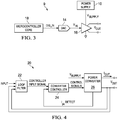
- FIGURE 3 illustrates a block diagram of selected components of an example audio IC 9 of a personal audio device, in accordance with embodiments of the present disclosure.
- a microcontroller core 18 may supply a digital audio input signal DIG_IN to a digital-to-analog converter (DAC) 14, which may convert the digital audio input signal to an analog signal V IN .
- DAC 14 may supply analog signal V IN to an amplifier 16 which may amplify or attenuate audio input signal V IN to provide a differential audio output signal V OUT , which may operate a speaker, a headphone transducer, a line level signal output, and/or other suitable output.
- DAC 14 may be an integral component of amplifier 16.
- a power supply 10 may provide the power supply rail inputs of amplifier 16.
- power supply 10 may comprise a battery.
- FIGURES 2 and 3 contemplate that audio IC 9 resides in a personal audio device, systems and methods described herein may also be applied to electrical and electronic systems and devices other than a personal audio device, including audio systems for use in a computing device larger than a personal audio device, an automobile, a building, or other structure.
- FIGURE 4 illustrates a block and circuit diagram of selected components of an example switched mode amplifier 20, in accordance with embodiments of the present disclosure.
- switched mode amplifier 20 may implement all or a portion of amplifier 16 described with respect to FIGURE 3 .
- switched mode amplifier 20 may comprise a loop filter 22, a converter controller 24, and a power converter 26.
- Loop filter 22 may comprise any system, device, or apparatus configured to receive an input signal (e.g., audio input signal V IN or a derivative thereof) and a feedback signal (e.g., audio output signal V OUT , a derivative thereof, or other signal indicative of audio output signal V OUT ) and based on such input signal and feedback signal, generate a controller input signal to be communicated to converter controller 24.
- a controller input signal may comprise a signal indicative of an integrated error between the input signal and the feedback signal.
- such controller input signal may comprise a signal indicative of a target current signal to be driven as an output current I OUT or a target voltage signal to be driven as an output voltage V OUT to a load coupled to the output terminals of power converter 26.
- Converter controller 24 may comprise any system, device, or apparatus configured to, based on the controller input signal, sequentially select among a plurality of switch configurations of power converter 26 and based on an input signal (e.g., input signal INPUT), output signal V OUT , detection of a peak current I pk of a power inductor of power converter 26, and/or other characteristics of switched mode amplifier 20, communicate a plurality of control signals to power converter 26 to apply a switch configuration from a plurality of switch configurations of switches of power converter 26 to selectively activate or deactivate each of the plurality of switches in order to transfer electrical energy from a power supply V SUPPLY to the load of switched-mode amplifier 20 in accordance with the input signal.
- converter controller 24 may control switches of a power converter 26 in order to regulate a common mode voltage V CM of the output terminals of power converter 26, as described in greater detail below.
- Power converter 26 may receive at its input a voltage V SUPPLY (e.g., provided by power supply 10) at its input, and may generate at its output audio output signal V OUT .
- voltage V SUPPLY may be received via input terminals including a positive input terminal and a negative input terminal which may be coupled to a ground voltage.
- power converter 26 may comprise a power inductor and a plurality of switches that are controlled by control signals received from converter controller 24 in order to convert voltage V SUPPLY to audio output signal V OUT , such that audio output signal V OUT is a function of the input signal to loop filter 22. Examples of power converter 26 are described in greater detail elsewhere in this disclosure.
- FIGURE 5 illustrates a circuit diagram of selected components of an example power converter 26, in accordance with embodiments of the present disclosure.
- power converter 26 depicted in FIGURE 5 may implement all or a portion of power converter 26 described with respect to FIGURE 4 .
- power converter 26 may receive at its input a voltage V SUPPLY (e.g., provided by power supply 10) at input terminals, including a positive input terminal and a negative input terminal which may be coupled to a ground voltage, and may generate at its output a differential output voltage V OUT .
- Power converter 26 may comprise a power inductor 62 and plurality of switches 51-59.
- Power inductor 62 may comprise any passive two-terminal electrical component which resists changes in electrical current passing through it and such that when electrical current flowing through it changes, a time-varying magnetic field induces a voltage in power inductor 62, in accordance with Faraday's law of electromagnetic induction, which opposes the change in current that created the magnetic field.
- Each switch 51-59 may comprise any suitable device, system, or apparatus for making a connection in an electric circuit when the switch is enabled (e.g., activated, closed, or on) and breaking the connection when the switch is disabled (e.g., deactivated, open, or off) in response to a control signal received by the switch.
- control signals for switches 51-59 e.g., control signals communicated from converter controller 24
- a switch 51-59 may comprise an n-type metal-oxide-semiconductor field-effect transistor.
- Switch 51 may be coupled between a positive input terminal of the supply voltage V SUPPLY and a first terminal of power inductor 62.
- Switch 52 may be coupled between the positive input terminal and a second terminal of power inductor 62.
- Switch 53 may be coupled between a negative input terminal of the supply voltage V SUPPLY (e.g., ground voltage) and the second terminal of power inductor 62.
- Switch 54 may be coupled between the negative input terminal (e.g., ground voltage) and the first terminal of power inductor 62.
- Switch 55 may be coupled between a positive output terminal of power converter 26 and the second terminal of power inductor 62.
- Switch 56 may be coupled between a negative output terminal of power converter 26 and the first terminal of power inductor 62.
- Switch 57 may be coupled between the negative output terminal of power converter 26 and the second input terminal (e.g., ground voltage).
- Switch 58 may be coupled between the positive output terminal of power converter 26 and the second input terminal (e.g., ground voltage).
- Switch 59 may be coupled between a common capacitor node and the second input terminal (e.g., ground voltage).
- power converter 26 may include a first output capacitor 66 coupled between the positive terminal of the output terminal of power converter 26 and the common capacitor node and a second output capacitor 68 coupled between the negative terminal of the output terminal of power converter 26 and the common capacitor node.
- Each output capacitor 66 and 68 may comprise a passive two-terminal electrical component used to store energy electrostatically in an electric field, and may generate a current in response to a time-varying voltage across the capacitor.
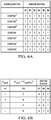
- FIGURES 6A and 6B illustrate tables showing various switch configurations that power converter 26 may operate in.
- FIGURE 6A depicts seven different switch configurations that converter controller 24 may select of switches 51-56, in accordance with embodiments of the present disclosure.
- converter controller 24 may enable switches 51 and 53 and disable switches 52, 54, 55, and 56, thus creating an electrical path from the positive terminal of the power supply, through power inductor 62, to the negative terminal (e.g., ground voltage) of the power supply in order to charge power inductor 62.
- converter controller 24 may enable switches 51 and 55 and disable switches 52, 53, 54, and 56, thus creating an electrical path from the positive terminal of the power supply, through power inductor 62, to a first output terminal of power converter 26 in order to transfer energy stored in power inductor 62 to a load of power converter 26.
- converter controller 24 may enable switches 54 and 55 and disable switches 51, 52, 53, and 56, thus creating an electrical path from a second output terminal of power converter 26, through power inductor 62, to the negative terminal of the power supply (e.g., ground voltage) in order to either discharge charge from the second output terminal to the negative terminal of the power supply or transfer energy stored in power inductor 62 to the second output terminal.
- the negative terminal of the power supply e.g., ground voltage
- controller 24 may enable switches 55 and 56 and disable switches 51, 52, 53, and 54, thus creating an electrical path from the first output terminal of power converter 26, through power inductor 62, to a second output terminal of power converter 26 in order to redistribute charge between the output terminals of power converter 26 in a differential output mode, or to discharge one of the output terminals to the negative terminal of the power supply in a single-ended mode, as described in greater detail below.
- converter controller 24 may enable switches 52 and 54 and disable switches 51, 53, 55, and 56, thus creating an electrical path from the positive terminal of the power supply, through power inductor 62, to the negative terminal (e.g., ground voltage) of the power supply in order to charge power inductor 62 in a polarity opposite to that of configuration CONFIG1 + .
- converter controller 24 may enable switches 52 and 56 and disable switches 51, 53, 54, and 55, thus creating an electrical path from the positive terminal of the power supply, through power inductor 62, to the second terminal of the output of power converter 26 in order to transfer energy stored in power inductor 62 to a load of power converter 26.
- converter controller 24 may enable switches 53 and 54 and disable switches 51, 52, 55, and 56, thus creating an electrical path from the first output terminal of power converter 26, through power inductor 62, to the negative terminal of the power supply (e.g., ground voltage) in order to either discharge charge from the first output terminal to the negative terminal of the power supply or transfer energy stored in power inductor 62 to the first output terminal.
- the negative terminal of the power supply e.g., ground voltage
- power converter 26 may comprise one or more additional switches which permit configurations similar to those above, but with the polarity of power inductor 26 reversed.
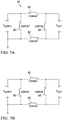
- FIGURES 7A and 7B illustrate equivalent circuit diagrams of selected components of power converter 26 operating in various phases of power converter 26 depicted in FIGURE 6A , in accordance with embodiments of the present disclosure.
- FIGURE 6B depicts three different switch configurations that converter controller 24 may select of switches 57, 58, and 59, based on polarity of output voltage V OUT and the magnitude of V OUT relative to V SUPPLY .
- converter controller 24 may enable switch 59 and disable switches 57 and 58, which may have the effect of making output voltage V OUT a differential voltage (e.g., with neither output terminal of the output of power converter 26 coupled to the second terminal of the power supply).
- converter controller 24 may enable switch 57 and disable switches 58 and 59, which may have the effect of making output voltage V OUT a single-ended voltage equal to the potential on the first output terminal of power converter 26.
- converter controller 24 may enable switch 58 and disable switches 57 and 59, which may have the effect of making output voltage V OUT a single-ended voltage equal to the potential on the second output terminal of power converter 26.
- converter controller 24 may control switches 51-59 of power converter 26 in order to generate output voltage V OUT based on an input signal (e.g., INPUT). For example, the number of phases in a switching cycle of power converter 26 and the switching configuration applied for each of such phases may be based on the desired output voltage V OUT and in some cases, whether a common mode V CM voltage of the output terminals of power converter 26 is to be increased or decreased in order to regulate common mode voltage V CM .
- converter controller 24 may control switches 51-59 of power converter 26 to operate in two phases per switching cycle in a first output voltage range when 0 ⁇
- V 1 is a predetermined threshold voltage greater or equal to zero and less than supply voltage V SUPPLY .
- converter controller 24 may apply configuration CONFIG1 + (or configuration CONFIG1 - ) and apply configuration CONFIG4 in a second phase T2 of operation in the first output voltage range (e.g., operating in a two-phase buck mode of operation).
- converter controller 24 may control switches 51-59 of power converter 26 to operate in three phases per switching cycle in a second output voltage range when V 1 ⁇
- V 2 is a predetermined threshold voltage greater than supply voltage V SUPPLY .
- switching cycles of power converter 26 may substantially be approximately equal in period (e.g., within manufacturing and operational tolerances that may cause generally insignificant differences in periodicity of switching cycles desired to be equal in period).
- the second output voltage range (e.g., V 1 ⁇
- first triphase subrange A power converter 26 may operate in a differential output mode (e.g., switch 59 is enabled and switches 57 and 58 are disabled such that neither output terminal is coupled to the negative input terminal of the power supply).
- power converter 26 may operate in a single-ended output mode (e.g., switch 59 is disabled and either of switch 57 or switch 58 is disabled based on the polarity of output voltage V OUT as shown in FIGURE 6B such that one of the output terminals is coupled to the negative input terminal of the power supply).
- a single-ended output mode e.g., switch 59 is disabled and either of switch 57 or switch 58 is disabled based on the polarity of output voltage V OUT as shown in FIGURE 6B such that one of the output terminals is coupled to the negative input terminal of the power supply.
- converter controller 24 may control switches 51-59 of power converter 26 to select any suitable order of switching configurations depending on a desired characteristic for power converter 26 (e.g., regulation of common mode voltage V CM of output terminals, optimization of power efficiency, minimization of electromagnetic interference, etc.).
- a desired characteristic for power converter 26 e.g., regulation of common mode voltage V CM of output terminals, optimization of power efficiency, minimization of electromagnetic interference, etc.
- FIGURE 8 illustrates a table depicting example phases and switching configurations associated with each phase for operation in first triphase subrange A
- FIGURE 9 illustrates a table depicting example phases and switching configurations associated with each phase for operation in second triphase subrange B, in accordance with embodiments of the present disclosure.
- converter controller 24 may control switches 51-59 of power converter 26 to operate in phases T1, T2, and T3 in each switching cycle of power converter 26.
- converter controller 24 may apply configuration CONFIG1 + in phase T1, apply configuration CONFIG2 + in phase T2 if common mode voltage V CM needs to be increased to regulate common mode voltage V CM to a desired common-mode voltage (e.g., V SUPPLY /2), apply configuration CONFIG3 - in phase T2 if common mode voltage V CM needs to be decreased to regulate common mode voltage V CM to the desired common-mode voltage, and apply configuration CONFIG4 in phase T3.
- V SUPPLY desired common-mode voltage
- converter controller 24 may apply configuration CONFIG1 - in phase T1, apply configuration CONFIG2 - in phase T2 if common mode voltage V CM needs to be increased to regulate common mode voltage V CM to a desired common-mode voltage (e.g., V SUPPLY /2), apply configuration CONFIG3 + in phase T2 if common mode voltage V CM needs to be decreased to regulate common mode voltage V CM to the desired common-mode voltage, and apply configuration CONFIG4 in phase T3.
- a desired common-mode voltage e.g., V SUPPLY /2
- V SUPPLY desired common-mode voltage
- converter controller 24 may control switches 51-59 of power converter 26 to operate in phases T1, T2, and T3 in each switching cycle of power converter 26.
- converter controller 24 may apply configuration CONFIG1 + in phase T1, apply configuration CONFIG2 + in phase T2, and apply configuration CONFIG3 + in phase T3.
- converter controller 24 may apply configuration CONFIG1 - in phase T1, apply configuration CONFIG2 - in phase T2, and apply configuration CONFIG3 - in phase T3.
- converter controller 24 may control switches 51-59 of power converter 26 in phases T1, T2, and T3 in each switching cycle of power converter 26 such that: (i) during phase T1, power inductor 62 is charged from the positive input terminal to the negative input terminal; (ii) during phase T2, power inductor 62 is coupled between a supply terminal and one of the output terminals; and (iii) during phase T3, power inductor 62 is either coupled between one of the output terminals and the negative supply terminal (single-ended mode) or between the two output terminals (differential mode).
- converter controller 24 may control switches 51-59 of power converter 26 to operate in two phases per switching cycle in a third output voltage range when
- converter controller 24 may apply configuration CONFIG1 + (or configuration CONFIG1 - ) and apply configuration CONFIG2 + (or configuration CONFIG2 - ) in a second phase T2 of operation in the third output voltage range (e.g., operating in a two-phase boost mode of operation).
- threshold voltage V 1 may equal 0, in which case the first output voltage range does not exist and converter controller 24 and power converter 26 do not operate in a two-phase switching in such a first output voltage range.
- threshold voltage V 2 may equal the maximum full scale voltage of output voltage V OUT , in which case the third output voltage range does not exist and converter controller 24 and power converter 26 do not operate in a two-phase switching in such a third output voltage range.
- V SUPPLY T 1 + V SUPPLY ⁇ V OUT / K T 2 + V OUT T 3 0
- T 1 , T 2 , and T 3 are the durations of periods T1, T2, and T3, respectively
- K is a constant having a value of 2 when the output of power converter 26 is differential (e.g., switches 57 and 58 are disabled) and a value of 1 when the output of power converter 26 is single-ended (e.g., one of switches 57 and 58 is enabled).
- converter controller 24 may also control a duration of at least two of the phases based on an input signal (e.g., input signal INPUT to loop filter 22 or the controller input signal to converter controller 24), output voltage V OUT , and/or another signal indicative of a desired voltage for output voltage V OUT .
- duration T 1 of phase T1 may be determined by a peak current I pk for inductor current IL
- duration T 2 of phase T2 may be a fixed duration of time
- duration T 3 of phase T3 may be determined by a peak current I pk for inductor current IL
- duration T 2 of phase T2 may be a fixed duration of time
- FIGURE 10 illustrates a graph depicting current versus time for switching cycles of the power converter of FIGURE 5 in tri-phase operation, in accordance with embodiments of the present disclosure.
- peak current I pk in first triphase subrange A e.g.,
- I pk I OUT T T + ⁇ 2 T 2 2 + ⁇ 3 T 3 T 2 + 2 T 3
- I mid I pk ⁇ ⁇ 2
- I min I pk ⁇ ⁇ 3 where I min is a minimum of inductor current IL during a switching cycle, I mid is inductor current IL at completion of phase T1 of a switching cycle, I OUT is a current flowing to a load between the output terminals of power converter 26, ⁇ 1 is a magnitude of change in inductor current
- each switching cycle of power converter 26 may be evaluated as a series of events.
- a switching configuration may be forced for a first phase having a forced duration. In some embodiments, such duration may be zero (such that a switching cycle operates in two phases).
- a peak current may be detected in a second phase.
- volt-second balancing may occur in a third phase until the next switching cycle.
- power converter 26 may more effectively and reliably transition between a buck mode of operation when output voltage V OUT is less than supply voltage V SUPPLY and a boost mode of operation when output voltage V OUT is greater than supply voltage V SUPPLY .
- converter controller 24 and power converter 26 may more effectively (as compared to traditional approaches) regulate common mode voltage of the output terminals of power converter 26, as each phase during operation in the differential mode couples an output terminal of power converter 26 to a power supply terminal via power inductor 62 or the other output terminal via power inductor 26.
- converter controller 24 and power converter 26 may permit maintenance of continuous peak current and/or continuous CCM current of power inductor 62 when switching between modes of operation (e.g., when switching between a buck or buck-boost mode for lower magnitudes of output voltage V OUT and a boost mode for higher magnitudes of V OUT ).
- FIGURE 11 illustrates a graph depicting example peak currents I pk and minimum currents I min for inductor current IL as a function of magnitude of output voltage V OUT for operation in a buck-boost mode and a boost mode of power converter 26, in accordance with embodiments of the present disclosure.
- converter controller 24 and power converter 26 may operate more efficiently from a power consumption perspective (as compared to traditional approaches) due to the fact that the T1 and T2 phases couple an output terminal of power converter 26 to a power supply terminal via power inductor 62, reducing losses and reducing peak-to-peak currents (which in turn may reduce electromagnetic interference radiation).
- the determination may be a qualitative determination. In other embodiments, such determination may be based on a time needed to measure peak current I pk , a direct current inductor current IL, and/or the mode of operation (e.g., buck, buck-boost, boost).
- the mode of operation e.g., buck, buck-boost, boost
- the determination of the fixed amount of time for the phase forced to have the fixed-time duration may be based on variation in a common mode voltage of the output terminals of power converter 26, the mode of operation (e.g., buck, buck-boost, boost), and/or timings needed to provide for smooth transitions between modes of operation (e.g., buck, buck-boost, boost).
- the mode of operation e.g., buck, buck-boost, boost
- timings needed to provide for smooth transitions between modes of operation e.g., buck, buck-boost, boost.
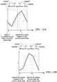
- converter controller 24 may in a differential output mode of power converter 26 (e.g., when switches 57 and 58 are disabled, for magnitudes of output voltage V OUT less than supply voltage V SUPPLY ), invoke quadrature switching of power converter 26 in order to control common mode voltage V CM of the output terminals of power converter 26.
- a fourth phase T4 may be used and converter controller 24 may cause ordering of switch configurations during such phases based on whether to increase or decrease the common mode voltage V CM of the output terminals of power converter 26.
- CONFIG3 + , CONFIG1 + , CONFIG2 + , and CONFIG4 may be used in phases T1, T2, T3, and T4 respectively to increase common mode voltage V CM over the switching cycle depicted in FIGURE 12A , as more charge may be added to the output terminals during phase T3 than is removed from the output terminals during phase T1.
- the order of CONFIG2 + , CONFIG1 + , CONFIG3 + , and CONFIG4 may be used in phases T1, T2, T3, and T4 respectively to decrease common mode voltage V CM over the switching cycle depicted in FIGURE 12B , as more charge may be removed from the output terminals during phase T3 than is added to the output terminals during phase T1.
- common mode voltage V CM may be increased or decreased, and the change in common mode voltage V CM may be controlled by controlling the durations of phases T1 and T3 employing CONFIG2 + and CONFIG3 + .
- durations of phases T1 and T3 in quadrature switching may be fixed, which may lead to a hysteretic control for common mode voltage V CM .
- durations of phases T1 and T3 may be adaptively controlled, allowing for accurate control of common mode voltage V CM .
- the sum of durations of phases T1 and T3 may be fixed but may be varied relative to each other in order to control a level of charging and discharging of the output terminals to control common mode voltage V CM .
- Quadrature switching may have additional benefits over the tri-phase switching earlier discussed.
- First, quadrature switching may allow for smaller changes in common mode voltage V CM per switching cycle.
- Second, quadrature switching may reduce electromagnetic interference as its switching waveform is more sinusoidal than that of triphase switching and provides greater control of where common mode energy is placed.
- Third, lower peak currents may be needed for quadrature switching, thus improving power efficiency.
- references in the appended claims to an apparatus or system or a component of an apparatus or system being adapted to, arranged to, capable of, configured to, enabled to, operable to, or operative to perform a particular function encompasses that apparatus, system, or component, whether or not it or that particular function is activated, turned on, or unlocked, as long as that apparatus, system, or component is so adapted, arranged, capable, configured, enabled, operable, or operative.
Landscapes
- Engineering & Computer Science (AREA)
- Power Engineering (AREA)
- Physics & Mathematics (AREA)
- Electromagnetism (AREA)
- Dc-Dc Converters (AREA)
Abstract
Description
- The present disclosure claims priority to
United States Provisional Patent Application Serial No. 62/148,567, filed April 16, 2015 - The present disclosure relates in general to circuits for audio devices, including without limitation personal audio devices such as wireless telephones and media players, and more specifically, to a switch mode amplifier including a reconfigurable switched mode converter for driving an audio transducer of an audio device.
- Personal audio devices, including wireless telephones, such as mobile/cellular telephones, cordless telephones, mp3 players, and other consumer audio devices, are in widespread use. Such personal audio devices may include circuitry for driving a pair of headphones or one or more speakers. Such circuitry often includes a speaker driver including a power amplifier for driving an audio output signal to headphones or speakers.
- One existing approach to driving an audio output signal is to employ a speaker driver, such as
speaker driver 100 depicted inFIGURE 1 .Speaker driver 100 may include an envelope-tracking boost converter 102 (e.g., a Class H amplifier) followed by a full-bridge output stage 104 (e.g., a Class D amplifier) which effectively operates as another converter stage.Boost converter 102 may include apower inductor 105,switches capacitor 110 arranged as shown. Full-bridge output stage 104 may includeswitches inductors capacitors - Speaker drivers, such as
speaker driver 100, suffer from numerous disadvantages. One disadvantage is that due to switching inoutput stage 104, such aspeaker driver 100 may give rise to large amounts of radiated electromagnetic radiation, which may cause interference with other electromagnetic signals. Such radiated electromagnetic interference may be mitigated by LC filters formed usinginductor 120 andcapacitor 122 andinductor 124 andcapacitor 126. However, such LC filters are often quite large in size, andcoupling capacitors speaker driver 100. - In addition, such architectures often do not handle large impulsive signals. To reduce power consumption, a power supply voltage VSUPPLY may be varied in accordance with the output signal, such that power supply voltage VSUPPLY may operate at lower voltage levels for lower output signal magnitudes. Thus, if a signal quickly increases, adequate time may not be present to increase voltage VSUPPLY, thus leading to signal clipping unless a delay is placed in the signal path. However, adding a delay to a signal path may cause incompatibility with other types of audio circuits, such as adaptive noise cancellation circuits.
- In accordance with the teachings of the present disclosure, one or more disadvantages and problems associated with existing approaches to driving an audio output signal to an audio transducer may be reduced or eliminated.
- In accordance with embodiments of the present disclosure, a switching power stage for producing an output voltage to a load may include a configurable switched mode power converter and a controller. The configurable switched mode power converter may include a power inductor, a plurality of switches arranged to sequentially operate in a plurality of switch configurations, and an output for producing the output voltage, the output comprising a first output terminal and a second output terminal. The controller may be configured to, for at least one range of magnitudes of the output voltage, control the plurality of switches to operate in at least three switching phases per switching cycle of the configurable switched mode power converter in order to generate the output voltage, wherein switching cycles of the configurable switched mode power converter are substantially approximately equal in period and control the plurality of switches to apply for each of the at least three switching phases a respective switch configuration of the plurality of switch configurations in order to achieve at least one of: maintenance of a continuous current of the power inductor throughout a dynamic range of the output voltage, maintenance of a continuous peak current of the power inductor throughout a dynamic range of the output voltage, regulation of a common mode voltage of the first output terminal and the second output terminal, minimization of electromagnetic interference of the power converter, and optimization of power efficiency of the power converter.
- In accordance with these and other embodiments of the present disclosure, a method for producing an output voltage to a load may include in a configurable switched mode power converter, comprising a power inductor, a plurality of switches arranged to sequentially operate in a plurality of switch configurations, and an output for producing the output voltage, the output comprising a first output terminal and a second output terminal, for at least one range of magnitudes of the output voltage, controlling the plurality of switches to operate in at least three switching phases per switching cycle of the configurable switched mode power converter in order to generate the output voltage, wherein switching cycles of the configurable switched mode power converter are substantially approximately equal in period. The method may also include controlling the plurality of switches to apply for each of the at least three switching phases a respective switch configuration of the plurality of switch configurations in order to achieve at least one of: maintenance of a continuous current of the power inductor throughout a dynamic range of the output voltage, maintenance of a continuous peak current of the power inductor throughout a dynamic range of the output voltage, regulation of a common mode voltage of the first output terminal and the second output terminal, minimization of electromagnetic interference of the power converter, and optimization of power efficiency of the power converter.
- In accordance with these and other embodiments of the present disclosure, a switching power stage for producing an output voltage to a load may include a configurable switched mode power converter and a controller. The configurable switched mode power converter may include a power inductor, a first supply terminal coupled to a first supply voltage, a second supply terminal coupled to a second supply voltage, an output for producing the output voltage, the output comprising a first output terminal and a second output terminal, and a plurality of switches including switches for respectively coupling the power inductor to each of the first supply terminal, the second supply terminal, the first output terminal, and the second output terminal, such that the plurality of switches provides at least seven switching configurations of the plurality of switches among of the first supply terminal, the second supply terminal, the first output terminal, and the second output terminal. The controller may be configured to enable at least three switching configurations of the at least seven switching configurations per switching cycle of the configurable switched mode power converter, wherein switching cycles of the configurable switched mode power converter are substantially approximately equal in period.
- In accordance with these and other embodiments of the present disclosure, a method for producing an output voltage to a load may include, in a configurable switched mode power converter, comprising a power inductor, a first supply terminal coupled to a first supply voltage, a second supply terminal coupled to a second supply voltage, an output for producing the output voltage, the output comprising a first output terminal and a second output terminal, and a plurality of switches including switches for respectively coupling the power inductor to each of the first supply terminal, the second supply terminal, the first output terminal, and the second output terminal, such that the plurality of switches provides at least seven switching configurations of the plurality of switches among of the first supply terminal, the second supply terminal, the first output terminal, and the second output terminal, enabling at least three switching configurations of the at least seven switching configurations per switching cycle of the configurable switched mode power converter, wherein switching cycles of the configurable switched mode power converter are substantially approximately equal in period.
- Technical advantages of the present disclosure may be readily apparent to one skilled in the art from the figures, description and claims included herein. The objects and advantages of the embodiments will be realized and achieved at least by the elements, features, and combinations particularly pointed out in the claims.
- It is to be understood that both the foregoing general description and the following detailed description are examples and explanatory and are not restrictive of the claims set forth in this disclosure.
- A more complete understanding of the present embodiments and advantages thereof may be acquired by referring to the following description taken in conjunction with the accompanying drawings, in which like reference numbers indicate like features, and wherein:
-
FIGURE 1 illustrates an example speaker driver, as is known in the relevant art; -
FIGURE 2 illustrates an example personal audio device, in accordance with embodiments of the present disclosure; -
FIGURE 3 illustrates a block diagram of selected components of an example audio integrated circuit of a personal audio device, in accordance with embodiments of the present disclosure; -
FIGURE 4 illustrates a block and circuit diagram of selected components of an example switched mode amplifier, in accordance with embodiments of the present disclosure; -
FIGURE 5 illustrates a circuit diagram of selected components of another example power converter, in accordance with embodiments of the present disclosure; -
FIGURES 6A and 6B illustrate tables showing various switch configurations that the power converter ofFIGURE 5 may operate in, in accordance with embodiments of the present disclosure; -
FIGURES 7A and 7B illustrate equivalent circuit diagrams of selected components of the power converter ofFIGURE 5 operating in various phases of a switching cycle of the power converter, in accordance with embodiments of the present disclosure; -
FIGURE 8 illustrates a table showing switch configurations that may be applied for each phases of operation of the power converter ofFIGURE 5 in tri-phase operation in a differential output mode, in accordance with embodiments of the present disclosure; -
FIGURE 9 illustrates a table showing switch configurations that may be applied for each phases of operation of the power converter ofFIGURE 5 in tri-phase operation in a single-ended output mode, in accordance with embodiments of the present disclosure; -
FIGURE 10 illustrates graphs depicting example waveforms of inductor current versus time for switching cycles of the power converter ofFIGURE 5 , in accordance with embodiments of the present disclosure; -
FIGURE 11 illustrates a graph depicting example peak currents and minimum currents for an inductor current of a power inductor of the power converter ofFIGURE 5 as a function of magnitude of output voltage for operation in a buck-boost mode and a boost mode of the power converter, in accordance with embodiments of the present disclosure; and -
FIGURES 12A and 12B each illustrates a graphs respectively depicting an example waveforms of inductor current versus time for switching cycles of the power converter ofFIGURE 5 employing quadrature switching, in accordance with embodiments of the present disclosure. -
FIGURE 2 illustrates an example personal audio device 1, in accordance with embodiments of the present disclosure.FIGURE 2 depicts personal audio device 1 coupled to aheadset 3 in the form of a pair ofearbud speakers Headset 3 depicted inFIGURE 2 is merely an example, and it is understood that personal audio device 1 may be used in connection with a variety of audio transducers, including without limitation, headphones, earbuds, in-ear earphones, and external speakers. Aplug 4 may provide for connection ofheadset 3 to an electrical terminal of personal audio device 1. Personal audio device 1 may provide a display to a user and receive user input using atouch screen 2, or alternatively, a standard liquid crystal display (LCD) may be combined with various buttons, sliders, and/or dials disposed on the face and/or sides of personal audio device 1. As also shown inFIGURE 2 , personal audio device 1 may include an audio integrated circuit (IC) 9 for generating an analog audio signal for transmission toheadset 3 and/or another audio transducer. -
FIGURE 3 illustrates a block diagram of selected components of anexample audio IC 9 of a personal audio device, in accordance with embodiments of the present disclosure. As shown inFIGURE 3 , amicrocontroller core 18 may supply a digital audio input signal DIG_IN to a digital-to-analog converter (DAC) 14, which may convert the digital audio input signal to an analog signal VIN. DAC 14 may supply analog signal VIN to anamplifier 16 which may amplify or attenuate audio input signal VIN to provide a differential audio output signal VOUT, which may operate a speaker, a headphone transducer, a line level signal output, and/or other suitable output. In some embodiments,DAC 14 may be an integral component ofamplifier 16. Apower supply 10 may provide the power supply rail inputs ofamplifier 16. In some embodiments,power supply 10 may comprise a battery. AlthoughFIGURES 2 and3 contemplate that audio IC 9 resides in a personal audio device, systems and methods described herein may also be applied to electrical and electronic systems and devices other than a personal audio device, including audio systems for use in a computing device larger than a personal audio device, an automobile, a building, or other structure. -
FIGURE 4 illustrates a block and circuit diagram of selected components of an example switchedmode amplifier 20, in accordance with embodiments of the present disclosure. In some embodiments, switchedmode amplifier 20 may implement all or a portion ofamplifier 16 described with respect toFIGURE 3 . As shown inFIGURE 4 , switchedmode amplifier 20 may comprise aloop filter 22, aconverter controller 24, and apower converter 26. -
Loop filter 22 may comprise any system, device, or apparatus configured to receive an input signal (e.g., audio input signal VIN or a derivative thereof) and a feedback signal (e.g., audio output signal VOUT, a derivative thereof, or other signal indicative of audio output signal VOUT) and based on such input signal and feedback signal, generate a controller input signal to be communicated to convertercontroller 24. In some embodiments, such controller input signal may comprise a signal indicative of an integrated error between the input signal and the feedback signal. In other embodiments, such controller input signal may comprise a signal indicative of a target current signal to be driven as an output current IOUT or a target voltage signal to be driven as an output voltage VOUT to a load coupled to the output terminals ofpower converter 26. -
Converter controller 24 may comprise any system, device, or apparatus configured to, based on the controller input signal, sequentially select among a plurality of switch configurations ofpower converter 26 and based on an input signal (e.g., input signal INPUT), output signal VOUT, detection of a peak current Ipk of a power inductor ofpower converter 26, and/or other characteristics of switchedmode amplifier 20, communicate a plurality of control signals topower converter 26 to apply a switch configuration from a plurality of switch configurations of switches ofpower converter 26 to selectively activate or deactivate each of the plurality of switches in order to transfer electrical energy from a power supply VSUPPLY to the load of switched-mode amplifier 20 in accordance with the input signal. Examples of switch configurations associated with each are described in greater detail elsewhere in this disclosure. In addition, in some embodiments,converter controller 24 may control switches of apower converter 26 in order to regulate a common mode voltage VCM of the output terminals ofpower converter 26, as described in greater detail below. -
Power converter 26 may receive at its input a voltage VSUPPLY (e.g., provided by power supply 10) at its input, and may generate at its output audio output signal VOUT. Although not explicitly shown inFIGURE 3 , in some embodiments, voltage VSUPPLY may be received via input terminals including a positive input terminal and a negative input terminal which may be coupled to a ground voltage. As described in greater detail in this disclosure,power converter 26 may comprise a power inductor and a plurality of switches that are controlled by control signals received fromconverter controller 24 in order to convert voltage VSUPPLY to audio output signal VOUT, such that audio output signal VOUT is a function of the input signal toloop filter 22. Examples ofpower converter 26 are described in greater detail elsewhere in this disclosure. -
FIGURE 5 illustrates a circuit diagram of selected components of anexample power converter 26, in accordance with embodiments of the present disclosure. In some embodiments,power converter 26 depicted inFIGURE 5 may implement all or a portion ofpower converter 26 described with respect toFIGURE 4 . As shown inFIGURE 5 ,power converter 26 may receive at its input a voltage VSUPPLY (e.g., provided by power supply 10) at input terminals, including a positive input terminal and a negative input terminal which may be coupled to a ground voltage, and may generate at its output a differential output voltage VOUT. Power converter 26 may comprise apower inductor 62 and plurality of switches 51-59.Power inductor 62 may comprise any passive two-terminal electrical component which resists changes in electrical current passing through it and such that when electrical current flowing through it changes, a time-varying magnetic field induces a voltage inpower inductor 62, in accordance with Faraday's law of electromagnetic induction, which opposes the change in current that created the magnetic field. - Each switch 51-59 may comprise any suitable device, system, or apparatus for making a connection in an electric circuit when the switch is enabled (e.g., activated, closed, or on) and breaking the connection when the switch is disabled (e.g., deactivated, open, or off) in response to a control signal received by the switch. For purposes of clarity and exposition, control signals for switches 51-59 (e.g., control signals communicated from converter controller 24) are not depicted although such control signals would be present to selectively enable and disable switches 51-59. In some embodiments, a switch 51-59 may comprise an n-type metal-oxide-semiconductor field-effect transistor.
Switch 51 may be coupled between a positive input terminal of the supply voltage VSUPPLY and a first terminal ofpower inductor 62.Switch 52 may be coupled between the positive input terminal and a second terminal ofpower inductor 62.Switch 53 may be coupled between a negative input terminal of the supply voltage VSUPPLY (e.g., ground voltage) and the second terminal ofpower inductor 62.Switch 54 may be coupled between the negative input terminal (e.g., ground voltage) and the first terminal ofpower inductor 62.Switch 55 may be coupled between a positive output terminal ofpower converter 26 and the second terminal ofpower inductor 62.Switch 56 may be coupled between a negative output terminal ofpower converter 26 and the first terminal ofpower inductor 62.Switch 57 may be coupled between the negative output terminal ofpower converter 26 and the second input terminal (e.g., ground voltage).Switch 58 may be coupled between the positive output terminal ofpower converter 26 and the second input terminal (e.g., ground voltage).Switch 59 may be coupled between a common capacitor node and the second input terminal (e.g., ground voltage). - In addition to switches 51-59 and
power inductor 62,power converter 26 may include afirst output capacitor 66 coupled between the positive terminal of the output terminal ofpower converter 26 and the common capacitor node and asecond output capacitor 68 coupled between the negative terminal of the output terminal ofpower converter 26 and the common capacitor node. Eachoutput capacitor - As described above, a
power converter 26 may operate in a plurality of different switch configurations.FIGURES 6A and 6B illustrate tables showing various switch configurations thatpower converter 26 may operate in. -
FIGURE 6A depicts seven different switch configurations thatconverter controller 24 may select of switches 51-56, in accordance with embodiments of the present disclosure. For example, in a configuration CONFIG1+,converter controller 24 may enableswitches switches power inductor 62, to the negative terminal (e.g., ground voltage) of the power supply in order to chargepower inductor 62. As another example, in a configuration CONFIG2+,converter controller 24 may enableswitches switches power inductor 62, to a first output terminal ofpower converter 26 in order to transfer energy stored inpower inductor 62 to a load ofpower converter 26. Further, in a configuration CONFIG3+,converter controller 24 may enableswitches switches power converter 26, throughpower inductor 62, to the negative terminal of the power supply (e.g., ground voltage) in order to either discharge charge from the second output terminal to the negative terminal of the power supply or transfer energy stored inpower inductor 62 to the second output terminal. In addition, in a configuration CONFIG4,controller 24 may enableswitches switches power converter 26, throughpower inductor 62, to a second output terminal ofpower converter 26 in order to redistribute charge between the output terminals ofpower converter 26 in a differential output mode, or to discharge one of the output terminals to the negative terminal of the power supply in a single-ended mode, as described in greater detail below. - In a configuration CONFIG1-,
converter controller 24 may enableswitches switches power inductor 62, to the negative terminal (e.g., ground voltage) of the power supply in order to chargepower inductor 62 in a polarity opposite to that of configuration CONFIG1+. In a configuration CONFIG2-,converter controller 24 may enableswitches switches power inductor 62, to the second terminal of the output ofpower converter 26 in order to transfer energy stored inpower inductor 62 to a load ofpower converter 26. In a configuration CONFIG3-,converter controller 24 may enableswitches switches power converter 26, throughpower inductor 62, to the negative terminal of the power supply (e.g., ground voltage) in order to either discharge charge from the first output terminal to the negative terminal of the power supply or transfer energy stored inpower inductor 62 to the first output terminal. - In some embodiments,
power converter 26 may comprise one or more additional switches which permit configurations similar to those above, but with the polarity ofpower inductor 26 reversed. I -
FIGURES 7A and 7B illustrate equivalent circuit diagrams of selected components ofpower converter 26 operating in various phases ofpower converter 26 depicted inFIGURE 6A , in accordance with embodiments of the present disclosure. -
FIGURE 6B depicts three different switch configurations thatconverter controller 24 may select ofswitches converter controller 24 may enableswitch 59 and disableswitches power converter 26 coupled to the second terminal of the power supply). When the magnitude of output voltage VOUT is greater than or equal to the supply voltage VSUPPLY and output voltage VOUT is positive,converter controller 24 may enableswitch 57 and disableswitches power converter 26. When the magnitude of output voltage VOUT is greater than or equal to the supply voltage VSUPPLY and output voltage VOUT is negative,converter controller 24 may enableswitch 58 and disableswitches power converter 26. - In operation,
converter controller 24 may control switches 51-59 ofpower converter 26 in order to generate output voltage VOUT based on an input signal (e.g., INPUT). For example, the number of phases in a switching cycle ofpower converter 26 and the switching configuration applied for each of such phases may be based on the desired output voltage VOUT and in some cases, whether a common mode VCM voltage of the output terminals ofpower converter 26 is to be increased or decreased in order to regulate common mode voltage VCM. - To illustrate,
converter controller 24 may control switches 51-59 ofpower converter 26 to operate in two phases per switching cycle in a first output voltage range when 0 ≤ |VOUT| < V1, wherein V1 is a predetermined threshold voltage greater or equal to zero and less than supply voltage VSUPPLY. For example, in a first phase T1 of operation in the first output voltage range,converter controller 24 may apply configuration CONFIG1+ (or configuration CONFIG1-) and apply configuration CONFIG4 in a second phase T2 of operation in the first output voltage range (e.g., operating in a two-phase buck mode of operation). In addition,converter controller 24 may control switches 51-59 ofpower converter 26 to operate in three phases per switching cycle in a second output voltage range when V1 ≤ |VOUT| < V2, wherein V2 is a predetermined threshold voltage greater than supply voltage VSUPPLY. In other words, for each switching cycle ofpower converter 26,power converter 26 may operate in three phases during the switching cycle, andpower converter 26 maintains a different switch configuration for each of the three phases. In embodiments of the present disclosure, switching cycles ofpower converter 26 may substantially be approximately equal in period (e.g., within manufacturing and operational tolerances that may cause generally insignificant differences in periodicity of switching cycles desired to be equal in period). - The second output voltage range (e.g., V1 ≤ |VOUT| < V2) may further be subdivided into a first triphase subrange A wherein V1 ≤ |VOUT| < VSUPPLY and a second triphase subrange B wherein VSUPPLY ≤ |VOUT| < V2. In first triphase subrange A,
power converter 26 may operate in a differential output mode (e.g., switch 59 is enabled and switches 57 and 58 are disabled such that neither output terminal is coupled to the negative input terminal of the power supply). In second triphase subrange B,power converter 26 may operate in a single-ended output mode (e.g., switch 59 is disabled and either ofswitch 57 orswitch 58 is disabled based on the polarity of output voltage VOUT as shown inFIGURE 6B such that one of the output terminals is coupled to the negative input terminal of the power supply). - In each of the sub-ranges of the second output voltage range,
converter controller 24 may control switches 51-59 ofpower converter 26 to select any suitable order of switching configurations depending on a desired characteristic for power converter 26 (e.g., regulation of common mode voltage VCM of output terminals, optimization of power efficiency, minimization of electromagnetic interference, etc.). For example,FIGURE 8 illustrates a table depicting example phases and switching configurations associated with each phase for operation in first triphase subrange A andFIGURE 9 illustrates a table depicting example phases and switching configurations associated with each phase for operation in second triphase subrange B, in accordance with embodiments of the present disclosure. - As shown in
FIGURE 8 , in first triphase subrange A,converter controller 24 may control switches 51-59 ofpower converter 26 to operate in phases T1, T2, and T3 in each switching cycle ofpower converter 26. When output voltage VOUT is positive,converter controller 24 may apply configuration CONFIG1+ in phase T1, apply configuration CONFIG2+ in phase T2 if common mode voltage VCM needs to be increased to regulate common mode voltage VCM to a desired common-mode voltage (e.g., VSUPPLY/2), apply configuration CONFIG3- in phase T2 if common mode voltage VCM needs to be decreased to regulate common mode voltage VCM to the desired common-mode voltage, and apply configuration CONFIG4 in phase T3. Similarly, when output voltage VOUT is negative,converter controller 24 may apply configuration CONFIG1- in phase T1, apply configuration CONFIG2- in phase T2 if common mode voltage VCM needs to be increased to regulate common mode voltage VCM to a desired common-mode voltage (e.g., VSUPPLY/2), apply configuration CONFIG3+ in phase T2 if common mode voltage VCM needs to be decreased to regulate common mode voltage VCM to the desired common-mode voltage, and apply configuration CONFIG4 in phase T3. - As shown in
FIGURE 9 ,converter controller 24 may control switches 51-59 ofpower converter 26 to operate in phases T1, T2, and T3 in each switching cycle ofpower converter 26. When output voltage VOUT is positive,converter controller 24 may apply configuration CONFIG1+ in phase T1, apply configuration CONFIG2+ in phase T2, and apply configuration CONFIG3+ in phase T3. Similarly, when output voltage VOUT is negative,converter controller 24 may apply configuration CONFIG1- in phase T1, apply configuration CONFIG2- in phase T2, and apply configuration CONFIG3- in phase T3. - Accordingly, when operating in the second output voltage range (e.g., V1 ≤ |VOUT| < V2),
converter controller 24 may control switches 51-59 ofpower converter 26 in phases T1, T2, and T3 in each switching cycle ofpower converter 26 such that: (i) during phase T1,power inductor 62 is charged from the positive input terminal to the negative input terminal; (ii) during phase T2,power inductor 62 is coupled between a supply terminal and one of the output terminals; and (iii) during phase T3,power inductor 62 is either coupled between one of the output terminals and the negative supply terminal (single-ended mode) or between the two output terminals (differential mode). - Further,
converter controller 24 may control switches 51-59 ofpower converter 26 to operate in two phases per switching cycle in a third output voltage range when |VOUT| > V2. For example, in a first phase T1 of operation in the third output voltage range,converter controller 24 may apply configuration CONFIG1+ (or configuration CONFIG1- ) and apply configuration CONFIG2+ (or configuration CONFIG2-) in a second phase T2 of operation in the third output voltage range (e.g., operating in a two-phase boost mode of operation). - Although the foregoing contemplates operation in three ranges of output voltage VOUT, in some embodiments, operation may take place in fewer than three ranges of operation. For example, in some embodiments, threshold voltage V1 may equal 0, in which case the first output voltage range does not exist and
converter controller 24 andpower converter 26 do not operate in a two-phase switching in such a first output voltage range. In these and other embodiments, threshold voltage V2 may equal the maximum full scale voltage of output voltage VOUT, in which case the third output voltage range does not exist andconverter controller 24 andpower converter 26 do not operate in a two-phase switching in such a third output voltage range. - In tri-phase operation in the second output voltage range (e.g., V1 ≤ |VOUT| < V2), assuming operation in a continuous conduction mode for
power inductor 62, the following volt-second equation must hold true in each switching cycle:
power converter 26 is differential (e.g., switches 57 and 58 are disabled) and a value of 1 when the output ofpower converter 26 is single-ended (e.g., one ofswitches - In these and other embodiments,
converter controller 24 may also control a duration of at least two of the phases based on an input signal (e.g., input signal INPUT toloop filter 22 or the controller input signal to converter controller 24), output voltage VOUT, and/or another signal indicative of a desired voltage for output voltage VOUT. For example, in some embodiments, duration T1 of phase T1 may be determined by a peak current Ipk for inductor current IL, duration T2 of phase T2 may be a fixed duration of time, and duration T3 of phase T3 may be the remainder of time within a switching cycle of power converter 26 (e.g., T3 = TT - T1- T2, where TT is a period of switching cycles of power converter 26). As another example, in other embodiments, duration T3 of phase T3 may be determined by a peak current Ipk for inductor current IL, duration T2 of phase T2 may be a fixed duration of time, and duration T1 of phase T1 may be the remainder of time within a switching cycle of power converter 26 (e.g., T1= TT - T2 - T3). -
FIGURE 10 illustrates a graph depicting current versus time for switching cycles of the power converter ofFIGURE 5 in tri-phase operation, in accordance with embodiments of the present disclosure. To determine peak current Ipk in first triphase subrange A (e.g., |VOUT| < VSUPPLY), the following equations may be used:


power converter 26, Δ1 is a magnitude of change in inductor current IL during phase T1, Δ2 is a magnitude of change in inductor current IL during phase T2, and Δ3 is a magnitude of change in inductor current IL during phase T3. - To determine peak current Ipk in second triphase subrange B (e.g., |VOUT| ≥ VSUPPLY), the following equations may be used:


- The foregoing equations may assume steady state conditions in which inductor current IL is the same at the end of a switching cycle as it is at the beginning of the switching cycle.
- Accordingly, each switching cycle of
power converter 26 may be evaluated as a series of events. In a first event, a switching configuration may be forced for a first phase having a forced duration. In some embodiments, such duration may be zero (such that a switching cycle operates in two phases). In a second event, a peak current may be detected in a second phase. In a third event, volt-second balancing may occur in a third phase until the next switching cycle. - By switching among at least three phases and controlling the order and durations of phases,
power converter 26 may more effectively and reliably transition between a buck mode of operation when output voltage VOUT is less than supply voltage VSUPPLY and a boost mode of operation when output voltage VOUT is greater than supply voltage VSUPPLY. - Also, by switching among at least three phases and controlling the order and durations of phases,
converter controller 24 andpower converter 26 may more effectively (as compared to traditional approaches) regulate common mode voltage of the output terminals ofpower converter 26, as each phase during operation in the differential mode couples an output terminal ofpower converter 26 to a power supply terminal viapower inductor 62 or the other output terminal viapower inductor 26. - In addition, by switching among three phases and controlling the order and durations of phases,
converter controller 24 andpower converter 26 may permit maintenance of continuous peak current and/or continuous CCM current ofpower inductor 62 when switching between modes of operation (e.g., when switching between a buck or buck-boost mode for lower magnitudes of output voltage VOUT and a boost mode for higher magnitudes of VOUT). For example,FIGURE 11 illustrates a graph depicting example peak currents Ipk and minimum currents Imin for inductor current IL as a function of magnitude of output voltage VOUT for operation in a buck-boost mode and a boost mode ofpower converter 26, in accordance with embodiments of the present disclosure. - Furthermore, by switching among at least three phases and controlling the order and durations of phases,
converter controller 24 andpower converter 26 may operate more efficiently from a power consumption perspective (as compared to traditional approaches) due to the fact that the T1 and T2 phases couple an output terminal ofpower converter 26 to a power supply terminal viapower inductor 62, reducing losses and reducing peak-to-peak currents (which in turn may reduce electromagnetic interference radiation). - Although the foregoing examples force a particular phase to have a fixed duration through switching cycles of a mode, in other embodiments of this disclosure, other phases may be forced to have a fixed duration through switching cycles of a mode. In some embodiments, the determination may be a qualitative determination. In other embodiments, such determination may be based on a time needed to measure peak current Ipk, a direct current inductor current IL, and/or the mode of operation (e.g., buck, buck-boost, boost). Furthermore, the determination of the fixed amount of time for the phase forced to have the fixed-time duration may be based on variation in a common mode voltage of the output terminals of
power converter 26, the mode of operation (e.g., buck, buck-boost, boost), and/or timings needed to provide for smooth transitions between modes of operation (e.g., buck, buck-boost, boost). - Although the foregoing discussion contemplates tri-phase switching per switching cycle of
power converter 26, in some embodiments,converter controller 24 may in a differential output mode of power converter 26 (e.g., when switches 57 and 58 are disabled, for magnitudes of output voltage VOUT less than supply voltage VSUPPLY), invoke quadrature switching ofpower converter 26 in order to control common mode voltage VCM of the output terminals ofpower converter 26. In quadrature switching, in addition to phases T1, T2, and T3 described above, a fourth phase T4 may be used andconverter controller 24 may cause ordering of switch configurations during such phases based on whether to increase or decrease the common mode voltage VCM of the output terminals ofpower converter 26. For example, as shown inFIGURE 12A , the order of CONFIG3+, CONFIG1+, CONFIG2+, and CONFIG4 may be used in phases T1, T2, T3, and T4 respectively to increase common mode voltage VCM over the switching cycle depicted inFIGURE 12A , as more charge may be added to the output terminals during phase T3 than is removed from the output terminals during phase T1. Likewise, as shown inFIGURE 12B , the order of CONFIG2+, CONFIG1+, CONFIG3+, and CONFIG4 may be used in phases T1, T2, T3, and T4 respectively to decrease common mode voltage VCM over the switching cycle depicted inFIGURE 12B , as more charge may be removed from the output terminals during phase T3 than is added to the output terminals during phase T1. Thus, depending on which of configurations CONFIG2+ and CONFIG3+ is ordered first in a switching cycle, common mode voltage VCM may be increased or decreased, and the change in common mode voltage VCM may be controlled by controlling the durations of phases T1 and T3 employing CONFIG2+ and CONFIG3+. - In some embodiments, durations of phases T1 and T3 in quadrature switching may be fixed, which may lead to a hysteretic control for common mode voltage VCM. In other embodiments, durations of phases T1 and T3 may be adaptively controlled, allowing for accurate control of common mode voltage VCM. In other embodiments, the sum of durations of phases T1 and T3 may be fixed but may be varied relative to each other in order to control a level of charging and discharging of the output terminals to control common mode voltage VCM.
- Quadrature switching may have additional benefits over the tri-phase switching earlier discussed. First, quadrature switching may allow for smaller changes in common mode voltage VCM per switching cycle. Second, quadrature switching may reduce electromagnetic interference as its switching waveform is more sinusoidal than that of triphase switching and provides greater control of where common mode energy is placed. Third, lower peak currents may be needed for quadrature switching, thus improving power efficiency.
- As used herein, when two or more elements are referred to as "coupled" to one another, such term indicates that such two or more elements are in electronic communication or mechanical communication, as applicable, whether connected indirectly or directly, with or without intervening elements.
- This disclosure encompasses all changes, substitutions, variations, alterations, and modifications to the exemplary embodiments herein that a person having ordinary skill in the art would comprehend. Similarly, where appropriate, the appended claims encompass all changes, substitutions, variations, alterations, and modifications to the exemplary embodiments herein that a person having ordinary skill in the art would comprehend. Moreover, reference in the appended claims to an apparatus or system or a component of an apparatus or system being adapted to, arranged to, capable of, configured to, enabled to, operable to, or operative to perform a particular function encompasses that apparatus, system, or component, whether or not it or that particular function is activated, turned on, or unlocked, as long as that apparatus, system, or component is so adapted, arranged, capable, configured, enabled, operable, or operative.
- All examples and conditional language recited herein are intended for pedagogical objects to aid the reader in understanding the invention and the concepts contributed by the inventor to furthering the art, and are construed as being without limitation to such specifically recited examples and conditions. Although embodiments of the present inventions have been described in detail, it should be understood that various changes, substitutions, and alterations could be made hereto without departing from the spirit and scope of the disclosure.
- Various aspects of embodiments will be described with reference to the following numbered statements:
- S1. A switching power stage for producing an output voltage to a load, comprising:
- a configurable switched mode power converter, comprising:
- a power inductor;
- a plurality of switches arranged to sequentially operate in a plurality of switch configurations; and
- an output for producing the output voltage, the output comprising a first output terminal and a second output terminal; and
- a controller configured to, for at least one range of magnitudes of the output voltage:
- control the plurality of switches to operate in at least three switching phases per switching cycle of the configurable switched mode power converter in order to generate the output voltage, wherein switching cycles of the configurable switched mode power converter are substantially approximately equal in period; and
- control the plurality of switches to apply for each of the at least three switching phases a respective switch configuration of the plurality of switch configurations in order to achieve at least one of:
- maintenance of a continuous current of the power inductor throughout a dynamic range of the output voltage;
- maintenance of a continuous peak current of the power inductor throughout a dynamic range of the output voltage;
- regulation of a common mode voltage of the first output terminal and the second output terminal;
- minimization of electromagnetic interference of the power converter; and
- optimization of power efficiency of the power converter.
- a configurable switched mode power converter, comprising:
- S2. The switching power stage of statement S1, wherein the plurality of switch configurations comprise:
- a first configuration wherein the plurality of switches are activated and deactivated such that the power inductor is coupled between a first input terminal of a power supply of the power converter and a second input terminal of the power supply;
- a second configuration wherein the plurality of switches are activated and deactivated such that the power inductor is coupled between the first input terminal and the first output terminal;
- a third configuration wherein the plurality of switches are activated and deactivated such that the power inductor is coupled between the first input terminal and the second output terminal;
- a fourth configuration wherein the plurality of switches are activated and deactivated such that the power inductor is coupled between the second input terminal and the first output terminal;
- a fifth configuration wherein the plurality of switches are activated and deactivated such that the power inductor is coupled between the second input terminal and the second output terminal; and
- a sixth configuration wherein the plurality of switches are activated and deactivated such that the power inductor is coupled between the first output terminal and the second output terminal.
- S3. The switching power stage of statement S2, wherein, in the first configuration, the power inductor is coupled to the first input terminal via a first terminal of the power inductor, and wherein the plurality of switch configurations comprise a seventh configuration wherein the plurality of switches are activated and deactivated such that the power inductor is coupled between the first input terminal and the second input terminal such that the power inductor is coupled to the first input terminal via a second terminal of the power inductor.
- S4. The switching power stage of statement S2, further comprising one or more additional configurations analogous to at least one of the first configuration, second configuration, third configuration, fourth configuration, fifth configuration, and sixth configuration in which the a polarity of the power inductor is reversed relative to that of the first configuration, second configuration, third configuration, fourth configuration, fifth configuration, and sixth configuration.
- S5. The switching power stage of statement S2, wherein for at least one of the at least one three phases, the configuration for such phase is selected based on a common mode voltage of the first output terminal and the second output terminal.
- S6. The switching power stage of statement S1, wherein the at least one range of magnitudes comprises a range of magnitudes greater than a first threshold voltage and magnitudes lesser than a second threshold voltage.
- S7. The switching power stage of statement S6, wherein the controller is further configured to for magnitudes of the output voltage outside of the range of magnitudes, control the plurality of switches to operate in two switching phases per switching cycle of the configurable switched mode power converter.
- S8. The switching power stage of statement S6, wherein the range of magnitudes comprises:
- a first subrange for magnitudes of the output voltage lesser than a supply voltage of a power supply the power converter, wherein the controller is further configured to operate the power converter in a differential output mode; and
- a second subrange for magnitudes of the output voltage greater than the supply voltage, wherein the controller is further configured to operate the power converter in a single-ended output mode in which one of the first output terminal and one of the second output terminal is coupled to an input terminal of the power supply during all of the at least three phases.
- S9. The switching power stage of statement S1, wherein the controller is further configured to control durations of the at least three phases by applying a volt-second balance for each switching cycle.
- S10. The switching power stage of statement S1, wherein the controller is further configured to control durations of at least one of the at least three phases based on at least one of:
- a peak current of one of the at least three phases and a duration of another of the at least three phases;
- duration of two of the at least three phases;
- peak currents of two of the at least three phases; and
- electrical charge transferred in two of the at least three phases.
- S11. A method for producing an output voltage to a load, comprising:
- in a configurable switched mode power converter, comprising a power inductor, a plurality of switches arranged to sequentially operate in a plurality of switch configurations, and an output for producing the output voltage, the output comprising a first output terminal and a second output terminal, for at least one range of magnitudes of the output voltage, controlling the plurality of switches to operate in at least three switching phases per switching cycle of the configurable switched mode power converter in order to generate the output voltage, wherein switching cycles of the configurable switched mode power converter are substantially approximately equal in period; and
- controlling the plurality of switches to apply for each of the at least three switching phases a respective switch configuration of the plurality of switch configurations in order to achieve at least one of:
- maintenance of a continuous current of the power inductor throughout a dynamic range of the output voltage;
- maintenance of a continuous peak current of the power inductor throughout a dynamic range of the output voltage;
- regulation of a common mode voltage of the first output terminal and the second output terminal;
- minimization of electromagnetic interference of the power converter; and
- optimization of power efficiency of the power converter.
- S12. The method of statement S11, wherein the plurality of switch configurations comprise:
- a first configuration wherein the plurality of switches are activated and deactivated such that the power inductor is coupled between a first input terminal of a power supply of the power converter and a second input terminal of the power supply;
- a second configuration wherein the plurality of switches are activated and deactivated such that the power inductor is coupled between the first input terminal and the first output terminal;
- a third configuration wherein the plurality of switches are activated and deactivated such that the power inductor is coupled between the first input terminal and the second output terminal;
- a fourth configuration wherein the plurality of switches are activated and deactivated such that the power inductor is coupled between the second input terminal and the first output terminal;
- a fifth configuration wherein the plurality of switches are activated and deactivated such that the power inductor is coupled between the second input terminal and the second output terminal; and
- a sixth configuration wherein the plurality of switches are activated and deactivated such that the power inductor is coupled between the first output terminal and the second output terminal.
- S13. The method of statement S12, wherein, in the first configuration, the power inductor is coupled to the first input terminal via a first terminal of the power inductor, and wherein the plurality of switch configurations comprise a seventh configuration wherein the plurality of switches are activated and deactivated such that the power inductor is coupled between the first input terminal and the second input terminal such that the power inductor is coupled to the first input terminal via a second terminal of the power inductor.
- S14. The method of statement S12, further comprising one or more additional configurations analogous to at least one of the first configuration, second configuration, third configuration, fourth configuration, fifth configuration, and sixth configuration in which the a polarity of the power inductor is reversed relative to that of the first configuration, second configuration, third configuration, fourth configuration, fifth configuration, and sixth configuration.
- S15. The method of statement S12, wherein for at least one of the at least one three phases, the configuration for such phase is selected based on a common mode voltage of the first output terminal and the second output terminal.
- S16. The method of statement S11, wherein the at least one range of magnitudes comprises a range of magnitudes greater than a first threshold voltage and magnitudes lesser than a second threshold voltage.
- S17. The method of statement S16, further comprising for magnitudes of the output voltage outside of the range of magnitudes, controlling the plurality of switches to operate in two switching phases per switching cycle of the configurable switched mode power converter.
- S18. The method of statement S16, wherein the range of magnitudes comprises:
- a first subrange for magnitudes of the output voltage lesser than a supply voltage of a power supply the power converter, wherein the controller is further configured to operate the power converter in a differential output mode; and
- a second subrange for magnitudes of the output voltage greater than the supply voltage, wherein the controller is further configured to operate the power converter in a single-ended output mode in which one of the first output terminal and one of the second output terminal is coupled to an input terminal of the power supply during all of the at least three phases.
- S19. The method of statement S11, wherein the controller is further configured to control durations of the at least three phases by applying a volt-second balance for each switching cycle.
- S20. The method of statement S11, further comprising controlling durations of at least one of the at least three phases based on at least one of:
- a peak current of one of the at least three phases and a duration of another of the at least three phases;
- duration of two of the at least three phases;
- peak currents of two of the at least three phases; and
- electrical charge transferred in two of the at least three phases.
- S21. A switching power stage for producing an output voltage to a load, comprising:
- a configurable switched mode power converter, comprising:
- a power inductor;
- a first supply terminal coupled to a first supply voltage;
- a second supply terminal coupled to a second supply voltage;
- an output for producing the output voltage, the output comprising a first output terminal and a second output terminal; and
- a plurality of switches including switches for respectively coupling the power inductor to each of the first supply terminal, the second supply terminal, the first output terminal, and the second output terminal, such that the plurality of switches provides at least seven switching configurations of the plurality of switches among of the first supply terminal, the second supply terminal, the first output terminal, and the second output terminal; and
- a controller configured to enable at least three switching configurations of the at least seven switching configurations per switching cycle of the configurable switched mode power converter, wherein switching cycles of the configurable switched mode power converter are substantially approximately equal in period.
- a configurable switched mode power converter, comprising:
- S22. The switching power stage of statement S21, wherein the controller is configured to enable three switching configurations of the at least seven switching configurations per switching cycle of the configurable switched mode power converter.
- S23. The switching power stage of statement S21, wherein one of the at least three switching configurations comprises the plurality of switches activated and deactivated such that the power inductor is coupled between the first supply terminal and the second supply terminal.
- S24. The switching power stage of statement S21, wherein one of the at least three switching configurations comprises the plurality of switches activated and deactivated such that one of the first supply terminal and the second supply terminal is coupled to one of the first output terminal and the second output terminal.
- S25. The switching power stage of statement S21, wherein one of the at least three switching configurations comprises the plurality of switches activated and deactivated such that the power inductor is coupled between the first output terminal and the second output terminal.
- S26. The switching power stage of statement S21, wherein the at least three switching configurations comprise four switching configurations.
- S27. The switching power stage of statement S26, wherein the four switching configurations comprise:
- a first switching configuration wherein the plurality of switches are activated and deactivated such that the power inductor is coupled between the first supply terminal and the second supply terminal;
- a second switching configuration wherein the plurality of switches are activated and deactivated such that the power inductor is coupled between the second supply terminal and the second output terminal;
- a third switching configuration wherein the plurality of switches are activated and deactivated such that the power inductor is coupled between the first output terminal and the second output terminal; and
- a fourth switching configuration wherein the plurality of switches are activated and deactivated such that the power inductor is coupled between the first supply terminal and the first output terminal.
- S28. The switching power stage of statement S27, wherein the controller is configured to enable only three of the first switching configuration, the second switching configuration, the third switching configuration, and the fourth switching configuration during a switching cycle of the configurable switched mode power converter.
- S29. The switching power stage of statement S27, wherein the controller is configured to enable all four of the first switching configuration, the second switching configuration, the third switching configuration, and the fourth switching configuration during a switching cycle of the configurable switched mode power converter.
- S30. A method for producing an output voltage to a load, comprising, in a configurable switched mode power converter, comprising a power inductor, a first supply terminal coupled to a first supply voltage, a second supply terminal coupled to a second supply voltage, an output for producing the output voltage, the output comprising a first output terminal and a second output terminal, and a plurality of switches including switches for respectively coupling the power inductor to each of the first supply terminal, the second supply terminal, the first output terminal, and the second output terminal, such that the plurality of switches provides at least seven switching configurations of the plurality of switches among of the first supply terminal, the second supply terminal, the first output terminal, and the second output terminal:
enabling at least three switching configurations of the at least seven switching configurations per switching cycle of the configurable switched mode power converter, wherein switching cycles of the configurable switched mode power converter are substantially approximately equal in period. - S31. The method of statement S30, further comprising enabling three switching configurations of the at least seven switching configurations per switching cycle of the configurable switched mode power converter.
- S32. The method of statement S30, wherein one of the at least three switching configurations comprises the plurality of switches activated and deactivated such that the power inductor is coupled between the first supply terminal and the second supply terminal.
- S33. The method of statement S30, wherein one of the at least three switching configurations comprises the plurality of switches activated and deactivated such that one of the first supply terminal and the second supply terminal is coupled to one of the first output terminal and the second output terminal.
- S34. The method of statement S30, wherein one of the at least three switching configurations comprises the plurality of switches activated and deactivated such that the power inductor is coupled between the first output terminal and the second output terminal.
- S35. The method of statement S30, wherein the at least three switching configurations comprise four switching configurations.
- S36. The method of statement S35, wherein the four switching configurations comprise:
- a first switching configuration wherein the plurality of switches are activated and deactivated such that the power inductor is coupled between the first supply terminal and the second supply terminal;
- a second switching configuration wherein the plurality of switches are activated and deactivated such that the power inductor is coupled between the second supply terminal and the second output terminal;
- a third switching configuration wherein the plurality of switches are activated and deactivated such that the power inductor is coupled between the first output terminal and the second output terminal; and
- a fourth switching configuration wherein the plurality of switches are activated and deactivated such that the power inductor is coupled between the first supply terminal and the first output terminal.
- S37. The method of statement S36, further comprising enabling only three of the first switching configuration, the second switching configuration, the third switching configuration, and the fourth switching configuration during a switching cycle of the configurable switched mode power converter.
- S38. The method of statement S36, further comprising enabling all four of the first switching configuration, the second switching configuration, the third switching configuration, and the fourth switching configuration during a switching cycle of the configurable switched mode power converter.
Claims (15)
- A switching power stage for producing an output voltage to a load, comprising:a configurable switched mode power converter, comprising:a power inductor;a first supply terminal coupled to a first supply voltage;a second supply terminal coupled to a second supply voltage;an output for producing the output voltage, the output comprising a first output terminal and a second output terminal; anda plurality of switches including switches for respectively coupling the power inductor to each of the first supply terminal, the second supply terminal, the first output terminal, and the second output terminal, such that the plurality of switches provides at least seven switching configurations of the plurality of switches among of the first supply terminal, the second supply terminal, the first output terminal, and the second output terminal; anda controller configured to enable at least three switching configurations of the at least seven switching configurations per switching cycle of the configurable switched mode power converter, wherein switching cycles of the configurable switched mode power converter are substantially approximately equal in period.
- The switching power stage of Claim 1, wherein the controller is configured to enable three switching configurations of the at least seven switching configurations per switching cycle of the configurable switched mode power converter.
- The switching power stage of Claim 1, wherein one of the at least three switching configurations comprises the plurality of switches activated and deactivated such that the power inductor is coupled between the first supply terminal and the second supply terminal.
- The switching power stage of Claim 1, wherein one of the at least three switching configurations comprises the plurality of switches activated and deactivated such that one of the first supply terminal and the second supply terminal is coupled to one of the first output terminal and the second output terminal.
- The switching power stage of Claim 1, wherein one of the at least three switching configurations comprises the plurality of switches activated and deactivated such that the power inductor is coupled between the first output terminal and the second output terminal.
- The switching power stage of Claim 1, wherein the at least three switching configurations comprise four switching configurations.
- The switching power stage of Claim 6, wherein the four switching configurations comprise:a first switching configuration wherein the plurality of switches are activated and deactivated such that the power inductor is coupled between the first supply terminal and the second supply terminal;a second switching configuration wherein the plurality of switches are activated and deactivated such that the power inductor is coupled between the second supply terminal and the second output terminal;a third switching configuration wherein the plurality of switches are activated and deactivated such that the power inductor is coupled between the first output terminal and the second output terminal; anda fourth switching configuration wherein the plurality of switches are activated and deactivated such that the power inductor is coupled between the first supply terminal and the first output terminal.
- The switching power stage of Claim 7, wherein the controller is configured to enable only three of the first switching configuration, the second switching configuration, the third switching configuration, and the fourth switching configuration during a switching cycle of the configurable switched mode power converter.
- The switching power stage of Claim 7, wherein the controller is configured to enable all four of the first switching configuration, the second switching configuration, the third switching configuration, and the fourth switching configuration during a switching cycle of the configurable switched mode power converter.
- A method for producing an output voltage to a load, comprising, in a configurable switched mode power converter, comprising a power inductor, a first supply terminal coupled to a first supply voltage, a second supply terminal coupled to a second supply voltage, an output for producing the output voltage, the output comprising a first output terminal and a second output terminal, and a plurality of switches including switches for respectively coupling the power inductor to each of the first supply terminal, the second supply terminal, the first output terminal, and the second output terminal, such that the plurality of switches provides at least seven switching configurations of the plurality of switches among of the first supply terminal, the second supply terminal, the first output terminal, and the second output terminal:
enabling at least three switching configurations of the at least seven switching configurations per switching cycle of the configurable switched mode power converter, wherein switching cycles of the configurable switched mode power converter are substantially approximately equal in period. - The method of Claim 10, further comprising enabling three switching configurations of the at least seven switching configurations per switching cycle of the configurable switched mode power converter.
- The method of Claim 10, wherein one of the at least three switching configurations comprises the plurality of switches activated and deactivated such that the power inductor is coupled between the first supply terminal and the second supply terminal.
- The method of Claim 10, wherein one of the at least three switching configurations comprises the plurality of switches activated and deactivated such that one of the first supply terminal and the second supply terminal is coupled to one of the first output terminal and the second output terminal.
- The method of Claim 10, wherein one of the at least three switching configurations comprises the plurality of switches activated and deactivated such that the power inductor is coupled between the first output terminal and the second output terminal.
- The method of Claim 10, wherein the at least three switching configurations comprise four switching configurations
Applications Claiming Priority (3)
| Application Number | Priority Date | Filing Date | Title |
|---|---|---|---|
| US201562148567P | 2015-04-16 | 2015-04-16 | |
| PCT/EP2016/058470 WO2016166356A1 (en) | 2015-04-16 | 2016-04-16 | Reconfigurable switched mode converter |
| EP16720739.8A EP3284171B1 (en) | 2015-04-16 | 2016-04-16 | Reconfigurable switched mode power converter |
Related Parent Applications (2)
| Application Number | Title | Priority Date | Filing Date |
|---|---|---|---|
| EP16720739.8A Division EP3284171B1 (en) | 2015-04-16 | 2016-04-16 | Reconfigurable switched mode power converter |
| EP16720739.8A Division-Into EP3284171B1 (en) | 2015-04-16 | 2016-04-16 | Reconfigurable switched mode power converter |
Publications (1)
| Publication Number | Publication Date |
|---|---|
| EP3916981A1 true EP3916981A1 (en) | 2021-12-01 |
Family
ID=55913582
Family Applications (2)
| Application Number | Title | Priority Date | Filing Date |
|---|---|---|---|
| EP21187729.5A Withdrawn EP3916981A1 (en) | 2015-04-16 | 2016-04-16 | Reconfigurable switched mode converter |
| EP16720739.8A Active EP3284171B1 (en) | 2015-04-16 | 2016-04-16 | Reconfigurable switched mode power converter |
Family Applications After (1)
| Application Number | Title | Priority Date | Filing Date |
|---|---|---|---|
| EP16720739.8A Active EP3284171B1 (en) | 2015-04-16 | 2016-04-16 | Reconfigurable switched mode power converter |
Country Status (6)
| Country | Link |
|---|---|
| US (1) | US10177657B2 (en) |
| EP (2) | EP3916981A1 (en) |
| KR (1) | KR102352409B1 (en) |
| CN (1) | CN107925385B (en) |
| GB (1) | GB2554016B (en) |
| WO (1) | WO2016166356A1 (en) |
Families Citing this family (5)
| Publication number | Priority date | Publication date | Assignee | Title |
|---|---|---|---|---|
| US9992826B1 (en) * | 2017-05-30 | 2018-06-05 | Osram Sylvania Inc. | Dual mode constant current LED driver |
| US11190100B2 (en) | 2018-07-11 | 2021-11-30 | Maxim Integrated Products, Inc. | Charging device |
| US11336178B2 (en) | 2019-01-29 | 2022-05-17 | Maxim Integrated Products, Inc. | Continuous conduction mode SIMO device |
| CN112152452B (en) * | 2019-06-26 | 2022-02-08 | 台达电子工业股份有限公司 | Power supply circuit and operation method |
| US11183932B2 (en) | 2020-01-08 | 2021-11-23 | Astec International Limited | Switch-mode AC-DC power converter for reducing common mode noise |
Citations (2)
| Publication number | Priority date | Publication date | Assignee | Title |
|---|---|---|---|---|
| WO2012055968A1 (en) * | 2010-10-27 | 2012-05-03 | Merus Aps | Audio amplifier using multi-level pulse width modulation |
| CN103956929A (en) * | 2014-04-02 | 2014-07-30 | 华为技术有限公司 | Inverter |
Family Cites Families (12)
| Publication number | Priority date | Publication date | Assignee | Title |
|---|---|---|---|---|
| GB2479445B (en) * | 2006-08-31 | 2011-11-30 | Wolfson Microelectronics Plc | DC-DC converter circuits and methods and apparatus including such circuits |
| EP2019481A1 (en) * | 2007-07-25 | 2009-01-28 | Danmarks Tekniske Universitet | Switch-mode DC-DC converter with multiple power transformers |
| US8305061B1 (en) * | 2008-06-04 | 2012-11-06 | National Semiconductor Corporation | Apparatus and method for digitally controlled buck-boost switching regulator |
| TW201034363A (en) | 2009-03-13 | 2010-09-16 | Richtek Technology Corp | Buck-boost power converter and its control method |
| US8466743B2 (en) | 2010-04-27 | 2013-06-18 | Broadcom Corporation | Ground-referenced common-mode amplifier circuit and related method |
| US8760003B2 (en) * | 2010-08-02 | 2014-06-24 | Denso Corporation | Vehicle-use power supply control apparatus and control apparatus for controlling electric rotating machine mounted on vehicle as main engine |
| CN102136797A (en) * | 2010-09-08 | 2011-07-27 | 上海岩芯电子科技有限公司 | Modulating method for noninverting Buck-Boost power inverter |
| US8773196B2 (en) | 2011-09-30 | 2014-07-08 | Clevech Corporation | Resource pooling amplifier |
| CN104205605B (en) * | 2012-03-26 | 2017-03-08 | 株式会社村田制作所 | DC-to-AC converter |
| JP5880239B2 (en) * | 2012-04-13 | 2016-03-08 | 株式会社ソシオネクスト | Power supply device and power supply control method |
| US9490644B2 (en) * | 2013-09-09 | 2016-11-08 | Apple Inc. | Reconfigurable compensator with large-signal stabilizing network |
| US10348114B2 (en) * | 2014-04-08 | 2019-07-09 | Whisper Energy Systems Inc. | Portable electrical energy storage and power processing device |
-
2016
- 2016-04-15 US US15/130,453 patent/US10177657B2/en active Active
- 2016-04-16 EP EP21187729.5A patent/EP3916981A1/en not_active Withdrawn
- 2016-04-16 WO PCT/EP2016/058470 patent/WO2016166356A1/en not_active Ceased
- 2016-04-16 CN CN201680034947.1A patent/CN107925385B/en active Active
- 2016-04-16 KR KR1020177032977A patent/KR102352409B1/en active Active
- 2016-04-16 EP EP16720739.8A patent/EP3284171B1/en active Active
- 2016-04-16 GB GB1718657.8A patent/GB2554016B/en active Active
Patent Citations (2)
| Publication number | Priority date | Publication date | Assignee | Title |
|---|---|---|---|---|
| WO2012055968A1 (en) * | 2010-10-27 | 2012-05-03 | Merus Aps | Audio amplifier using multi-level pulse width modulation |
| CN103956929A (en) * | 2014-04-02 | 2014-07-30 | 华为技术有限公司 | Inverter |
Also Published As
| Publication number | Publication date |
|---|---|
| US20160308445A1 (en) | 2016-10-20 |
| WO2016166356A4 (en) | 2017-01-05 |
| KR102352409B1 (en) | 2022-01-18 |
| EP3284171A1 (en) | 2018-02-21 |
| GB2554016A (en) | 2018-03-21 |
| CN107925385A (en) | 2018-04-17 |
| GB2554016B (en) | 2021-10-13 |
| GB201718657D0 (en) | 2017-12-27 |
| KR20180013883A (en) | 2018-02-07 |
| WO2016166356A1 (en) | 2016-10-20 |
| EP3284171B1 (en) | 2021-09-08 |
| CN107925385B (en) | 2021-08-03 |
| US10177657B2 (en) | 2019-01-08 |
Similar Documents
| Publication | Publication Date | Title |
|---|---|---|
| EP3103194B1 (en) | Switch mode amplifier | |
| US9654056B2 (en) | Switched mode converter with low-voltage linear mode | |
| US9831839B2 (en) | Power stage with switched mode amplifier and linear amplifier | |
| KR102493533B1 (en) | Multi-Input/Multi-Output Switching Converter | |
| US10177657B2 (en) | Reconfigurable switched mode converter | |
| US10659887B2 (en) | High efficiency transducer driver | |
| CN113474983A (en) | Enhanced multi-level boost converter | |
| GB2533994A (en) | Power stage with switched mode amplifier and linear amplifier | |
| US20170373600A1 (en) | Multi-mode switching power converter |
Legal Events
| Date | Code | Title | Description |
|---|---|---|---|
| PUAI | Public reference made under article 153(3) epc to a published international application that has entered the european phase |
Free format text: ORIGINAL CODE: 0009012 |
|
| STAA | Information on the status of an ep patent application or granted ep patent |
Free format text: STATUS: THE APPLICATION HAS BEEN PUBLISHED |
|
| AC | Divisional application: reference to earlier application |
Ref document number: 3284171 Country of ref document: EP Kind code of ref document: P |
|
| AK | Designated contracting states |
Kind code of ref document: A1 Designated state(s): AL AT BE BG CH CY CZ DE DK EE ES FI FR GB GR HR HU IE IS IT LI LT LU LV MC MK MT NL NO PL PT RO RS SE SI SK SM TR |
|
| B565 | Issuance of search results under rule 164(2) epc |
Effective date: 20211102 |
|
| STAA | Information on the status of an ep patent application or granted ep patent |
Free format text: STATUS: REQUEST FOR EXAMINATION WAS MADE |
|
| 17P | Request for examination filed |
Effective date: 20220531 |
|
| RBV | Designated contracting states (corrected) |
Designated state(s): AL AT BE BG CH CY CZ DE DK EE ES FI FR GB GR HR HU IE IS IT LI LT LU LV MC MK MT NL NO PL PT RO RS SE SI SK SM TR |
|
| STAA | Information on the status of an ep patent application or granted ep patent |
Free format text: STATUS: THE APPLICATION IS DEEMED TO BE WITHDRAWN |
|
| 18D | Application deemed to be withdrawn |
Effective date: 20221101 |